data sheet model - futureelectronics.com semiconductor...gpio / pin cntl 4 x ssp 2 x i2c 2x saif...
TRANSCRIPT

Freescale SemiconductorData Sheet: Advance Information
Document Number: IMX28CECRev. 0, 09/2010
i.MX28
Package InformationPlastic package
Case 5284 14 x 14 mm, 0.8 mm Pitch
Ordering Information
See Table 1 on page 3 for ordering information.
i.MX28 Applications Processor Data Sheet for Consumer Products
Silicon Version 1.2
Contents1. Introduction . . . . . . . . . . . . . . . . . . . . . . . . . . . . . . . . . . . . 1
1.1. Device Features . . . . . . . . . . . . . . . . . . . . . . . . . . . 21.2. Ordering Information & Functional Part Differences 31.3. Block Diagram . . . . . . . . . . . . . . . . . . . . . . . . . . . . 5
2. Features . . . . . . . . . . . . . . . . . . . . . . . . . . . . . . . . . . . . . . 52.1. Special Signal Considerations . . . . . . . . . . . . . . . 10
3. Electrical Characteristics . . . . . . . . . . . . . . . . . . . . . . . . 113.1. i.MX28 Device-Level Conditions . . . . . . . . . . . . . . 113.2. I/O DC Parameters . . . . . . . . . . . . . . . . . . . . . . . . 193.3. I/O AC Timing and Parameters . . . . . . . . . . . . . . . 233.4. Module Timing and Electrical Parameters . . . . . . 27
4. Package Information and Contact Assignment . . . . . . . 594.1. 289-Ball MAPBGA—Case 14 x 14 mm,
0.8 mm Pitch . . . . . . . . . . . . . . . . . . . . . . . . . . . . . 634.2. Ground, Power, Sense, and Reference Contact
Assignments . . . . . . . . . . . . . . . . . . . . . . . . . . . . . 604.3. Signal Contact Assignments . . . . . . . . . . . . . . . . . 614.4. i.MX287 Ball Map . . . . . . . . . . . . . . . . . . . . . . . . . 644.5. i.MX286 Ball Map . . . . . . . . . . . . . . . . . . . . . . . . . 654.6. i.MX283 Ball Map . . . . . . . . . . . . . . . . . . . . . . . . . 66
5. Revision History . . . . . . . . . . . . . . . . . . . . . . . . . . . . . . . 67
1 IntroductionThe i.MX28 is a low-power, high-performance applications processor optimized for the general embedded industrial and consumer marketsindustrial and consumer markets.The core of the i.MX28 is Freescale's fast, proven, power-efficient implementation of the ARM926EJ-S™ core, with speeds of up to 454 MHz.
The device is suitable for a wide range of applications, including the following:
• Human-machine interface (HMI) panels: industrial, home
• Industrial drive, PLC, I/O control display, factory robotics display, graphical remote controls
• Handheld scanners and printers
© Freescale Semiconductor, Inc., 2010. All rights reserved.
• Patient-monitoring devices, portable medical
• Smart energy meters, energy gateways
• Media phones, media gateways
The integrated Power Management Unit (PMU) on the i.MX28 is composed of a triple output DC-DC switching converter and multiple linear regulators, to provide power sequencing for the device and its I/O peripherals such as memories and SD cards, as well as provide battery charging capability for Li-Ion batteries.
The i.MX28 processor includes an additional 128-Kbyte on-chip SRAM to make the device ideal for eliminating external RAM in applications with small footprint RTOS.
The i.MX28 supports connections to various types of external memories, such as mobile DDR, DDR2 and LV-DDR2, SLC and MLC NAND Flash.
The i.MX28 can be connected to a variety of external devices such as high-speed USB2.0 OTG, CAN, 10/100 Ethernet, and SD/SDIO/MMC.
1.1 Device FeaturesThe following includes features of the i.MX28:
• ARM926EJ-S CPU running at 454 MHz:
— 16-Kbyte instruction cache and 32-Kbyte data cache
— ARM embedded trace macrocell (CoreSight™ ETM9™)
— Parallel JTAG interface
• 128 KBytes of integrated low-power on-chip SRAM
• 128 KBytes of integrated mask-programmable on-chip ROM
• 1280 bits of on-chip one-time-programmable (OCOTP) ROM
• 16-bit mobile DDR (mDDR) (1.8 V), DDR2 (1.8 V) and LV-DDR2 (1.5 V), up to 200 MHz DDR clock frequency with voltage overdrive
• Up to eight NAND flash memory interfaces with up to 20-bit BCH ECC
• Four Synchronous Serial Ports (SSP) for SDIO/MMC/MS/SPI. Two can be used for SDIO/MMC/MS interfaces (supports SD2.0, eMMC4.4 and MSPro), and all can be used for the SPI interface.
• Two 10/100-Mbps Ethernet MACs compatible with IEEE Std 802.3™, supporting IEEE Std 1588™–compatible hardware timestamp and one 3-port L2 switch; also supports 50-MHz/25-MHz clock output for external Ethernet PHY
• Two 2.0B protocol–compatible Controller Area Network (CAN) interfaces
• One USB2.0 OTG device/host controller and PHY
• One USB2.0 host controller and PHY
• LCD controller, up to 24-bit RGB (DOTCK) modes and 24-bit system-mode
• Pixel-processing pipeline (PXP) supports full path from color-space conversion, scaling, alpha-blending to rotation without intermediate memory access.
i.MX28 Applications Processor Data Sheet for Consumer Products, Rev. 0
2 Freescale Semiconductor
• SPDIF transmitter
• Dual serial audio interface (SAIF) to support full-duplex transmit and receive operations; each SAIF supports three stereo pairs
• Five application Universal Asynchronous Receiver-Transmitters (UARTs), up to 3.25 Mbps with hardware flow control
• One debug UART operating at up to 115 Kb/s using programmed I/O
• Two I2C master/slave interfaces, up to 400 kbps
• Four 32-bit timers and a rotary decoder
• Eight Pulse Width Modulators (PWMs)
• Real-time clock (RTC)
• GPIO with interrupt capability
• Power Management Unit (PMU) supports a triple output DC-DC switching converter, multiple linear regulators, battery charger, and detector.
• 16-channel Low-Resolution A/D Converter (LRADC)
• 4/5-wire touchscreen controller
• Up to 8X8 keypad matrix with button-detect circuit
• 8-channel High Speed A/D Converter (HSADC), up to 2 Msps data rate
• Security features:
— Read-only unique ID for Digital Rights Management (DRM) algorithms
— Secure boot using 128-bit AES hardware decryption
— SHA-1 and SHA256 hashing hardware
— High assurance boot (HAB4)
• Offered in 289-pin Ball Grid Array (BGA)
1.2 Ordering Information & Functional Part DifferencesTable 1 provides the ordering information for the i.MX28.
Table 1. Ordering Information
Part Number Projected Temperature Range (°C) Package
MCIMX283DVM4B –20 to +70 14 x 14 mm, 0.8 mm pitch, MAPBGA-289
MCIMX283CVM4B –40 to +85 14 x 14 mm, 0.8 mm pitch, MAPBGA-289
MCIMX286DVM4B –20 to +70 14 x 14 mm, 0.8 mm pitch, MAPBGA-289
MCIMX286CVM4B –40 to +85 14 x 14 mm, 0.8 mm pitch, MAPBGA-289
MCIMX287CVM4B –40 to +85 14 x 14 mm, 0.8 mm pitch, MAPBGA-289
i.MX28 Applications Processor Data Sheet for Consumer Products, Rev. 0
Freescale Semiconductor 3
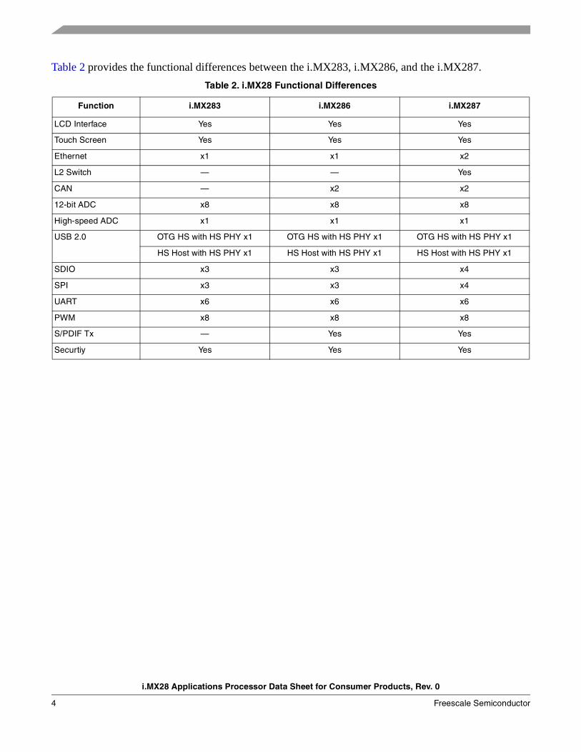
Table 2 provides the functional differences between the i.MX283, i.MX286, and the i.MX287.
Table 2. i.MX28 Functional Differences
Function i.MX283 i.MX286 i.MX287
LCD Interface Yes Yes Yes
Touch Screen Yes Yes Yes
Ethernet x1 x1 x2
L2 Switch — — Yes
CAN — x2 x2
12-bit ADC x8 x8 x8
High-speed ADC x1 x1 x1
USB 2.0 OTG HS with HS PHY x1 OTG HS with HS PHY x1 OTG HS with HS PHY x1
HS Host with HS PHY x1 HS Host with HS PHY x1 HS Host with HS PHY x1
SDIO x3 x3 x4
SPI x3 x3 x4
UART x6 x6 x6
PWM x8 x8 x8
S/PDIF Tx — Yes Yes
Securtiy Yes Yes Yes
i.MX28 Applications Processor Data Sheet for Consumer Products, Rev. 0
4 Freescale Semiconductor
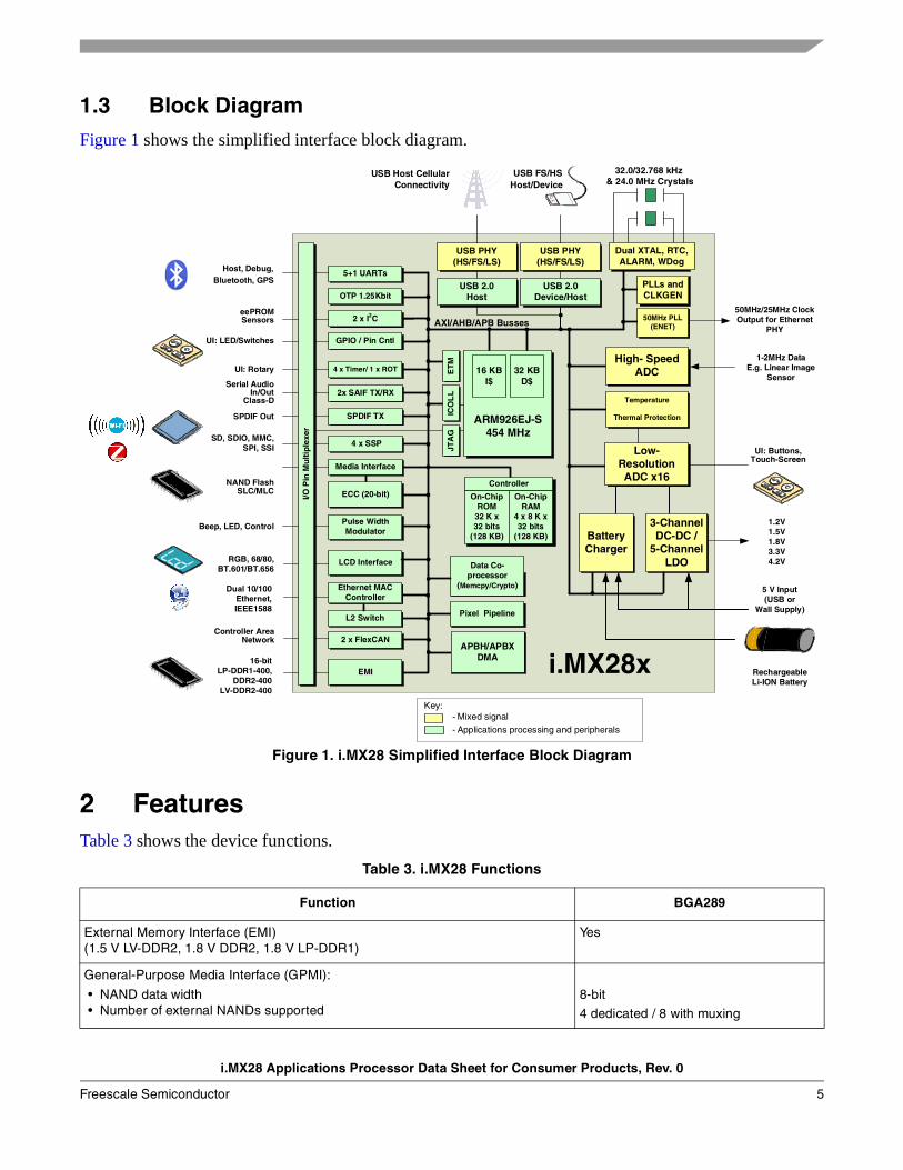
1.3 Block DiagramFigure 1 shows the simplified interface block diagram.
Figure 1. i.MX28 Simplified Interface Block Diagram
2 FeaturesTable 3 shows the device functions.
Table 3. i.MX28 Functions
Function BGA289
External Memory Interface (EMI)(1.5 V LV-DDR2, 1.8 V DDR2, 1.8 V LP-DDR1)
Yes
General-Purpose Media Interface (GPMI):
• NAND data width • Number of external NANDs supported
8-bit
4 dedicated / 8 with muxing
i.MX28x
AXI/AHB/APB Busses
16-bitLP-DDR1-400,
DDR2-400LV-DDR2-400
NAND FlashSLC/MLC
SD, SDIO, MMC, SPI, SSI
eePROM Sensors
UI: LED/Switches
5 V Input(USB or
Wall Supply)
Beep, LED, Control
Serial Audio In/Out
Class-D
UI: Rotary
1.2V1.5V1.8V3.3V4.2V
32.0/32.768 kHz & 24.0 MHz Crystals
Host, Debug,
RGB, 68/80, BT.601/BT.656
SPDIF Out
Rechargeable Li-ION Battery
UI: Buttons,Touch-Screen
SPDIF TX
Media Interface
5+1 UARTs
OTP 1.25Kbit
GPIO / Pin Cntl
4 x SSP
2 x I2C
2x SAIF TX/RX
Pulse Width Modulator
ECC (20-bit)
4 x Timer/ 1 x ROT
USBDual XTAL, RTC, ALARM, WDog
ICO
LL
Data Co-processor
(Memcpy/Crypto)
DSPARM926EJ-S
454 MHz
16 KBI$
32 KBD$
JTA
G
Key:- Mixed signal- Applications processing and peripherals
ET
M
Pixel Pipeline
LCD Interface
EMI
PLLs and CLKGEN
On-Chip ROM
32 K x32 bits
(128 KB)
On-Chip RAM
4 x 8 K x32 bits
(128 KB)
Controller
Dual 10/100Ethernet, IEEE1588
1-2MHz DataE.g. Linear Image
Sensor
3-Channel DC-DC /
5-Channel LDO
Low-Resolution ADC x16
BatteryCharger
Temperature
Thermal Protection
Controller Area Network
Gen
eral
Pu
rpo
se In
pu
t/O
utp
ut
I/O P
in M
ult
iple
xer
APBH/APBX DMA
High- Speed ADC
Bluetooth, GPS
USB FS/HS
USBUSB PHY
(HS/FS/LS)
USBUSB 2.0
Device/Host
USB
USB
USB PHY(HS/FS/LS)
USB 2.0Host
USB Host CellularConnectivity Host/Device
Thermal Protection
50MHz PLL (ENET)
50MHz/25MHz Clock Output for Ethernet
PHY
L2 Switch
Ethernet MAC Controller
2 x FlexCAN
i.MX28 Applications Processor Data Sheet for Consumer Products, Rev. 0
Freescale Semiconductor 5
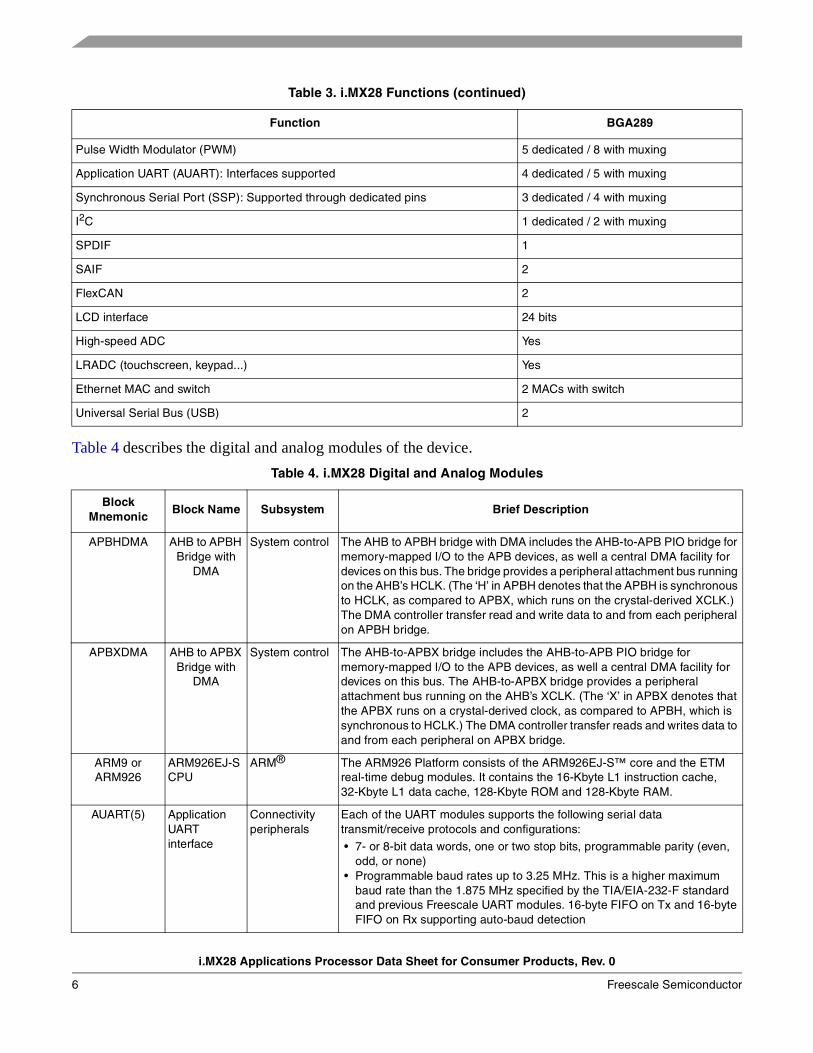
Table 4 describes the digital and analog modules of the device.
Pulse Width Modulator (PWM) 5 dedicated / 8 with muxing
Application UART (AUART): Interfaces supported 4 dedicated / 5 with muxing
Synchronous Serial Port (SSP): Supported through dedicated pins 3 dedicated / 4 with muxing
I2C 1 dedicated / 2 with muxing
SPDIF 1
SAIF 2
FlexCAN 2
LCD interface 24 bits
High-speed ADC Yes
LRADC (touchscreen, keypad...) Yes
Ethernet MAC and switch 2 MACs with switch
Universal Serial Bus (USB) 2
Table 4. i.MX28 Digital and Analog Modules
Block Mnemonic
Block Name Subsystem Brief Description
APBHDMA AHB to APBH Bridge with
DMA
System control The AHB to APBH bridge with DMA includes the AHB-to-APB PIO bridge for memory-mapped I/O to the APB devices, as well a central DMA facility for devices on this bus. The bridge provides a peripheral attachment bus running on the AHB’s HCLK. (The ‘H’ in APBH denotes that the APBH is synchronous to HCLK, as compared to APBX, which runs on the crystal-derived XCLK.) The DMA controller transfer read and write data to and from each peripheral on APBH bridge.
APBXDMA AHB to APBX Bridge with
DMA
System control The AHB-to-APBX bridge includes the AHB-to-APB PIO bridge for memory-mapped I/O to the APB devices, as well a central DMA facility for devices on this bus. The AHB-to-APBX bridge provides a peripheral attachment bus running on the AHB’s XCLK. (The ‘X’ in APBX denotes that the APBX runs on a crystal-derived clock, as compared to APBH, which is synchronous to HCLK.) The DMA controller transfer reads and writes data to and from each peripheral on APBX bridge.
ARM9 or ARM926
ARM926EJ-S CPU
ARM® The ARM926 Platform consists of the ARM926EJ-S™ core and the ETM real-time debug modules. It contains the 16-Kbyte L1 instruction cache, 32-Kbyte L1 data cache, 128-Kbyte ROM and 128-Kbyte RAM.
AUART(5) Application UART interface
Connectivity peripherals
Each of the UART modules supports the following serial data transmit/receive protocols and configurations:
• 7- or 8-bit data words, one or two stop bits, programmable parity (even, odd, or none)
• Programmable baud rates up to 3.25 MHz. This is a higher maximum baud rate than the 1.875 MHz specified by the TIA/EIA-232-F standard and previous Freescale UART modules. 16-byte FIFO on Tx and 16-byte FIFO on Rx supporting auto-baud detection
Table 3. i.MX28 Functions (continued)
Function BGA289
i.MX28 Applications Processor Data Sheet for Consumer Products, Rev. 0
6 Freescale Semiconductor
BCH Bit-correcting ECC accelerator
Connectivity peripherals
The Bose, Ray-Chaudhuri, Hocquenghem (BCH) Encoder and Decoder module is capable of correcting from 2 to 20 single bit errors within a block of data no larger than about 900 bytes (512 bytes is typical) in applications such as protecting data and resources stored on modern NAND flash devices.
BSI Boundary Scan Interface
Connectivity peripherals
The boundary scan interface is provided to enable board level testing.
There are five pins on the device which is used to implement the IEEE Std 1149.1™ boundary scan protocol.
CLKCTRL Clock control module
Clocks The clock control module, or CLKCTRL, generates the clock domains for all components in the i.MX28 system. The crystal clock or PLL clock are the two fundamental sources used to produce most of the clock domains. For lower performance and reduced power consumption, the crystal clock is selected. The PLL is selected for higher performance requirements but requires increased power consumption. In most cases, when the PLL is used as the source, a Phase Fractional Divider (PFD) can be programmed to reduce the PLL clock frequency by up to a factor of 2.
DCP Data co-processor
Security This module provides support for general encryption and hashing functions typically used for security functions. Because its basic job is moving data from memory to memory, it also incorporates a memory-copy (memcopy) function for both debugging and as a more efficient method of copying data between memory blocks than the DMA-based approach.
DFLPT Default first-level page table
System control The DFLPT provides a unique method of implementing the ARM MMU first-level page table (L1PT) using a hardware-based approach.
DIGCTL Digital control and on-chip RAM
System control The digital control module includes sections on controlling the SRAM, the performance monitors, high-entropy pseudo-random number seed, free-running microseconds counter, and other chip control functions.
DUART Debug UART Connectivity peripherals
The Debug UART performs the following data conversions:
• Serial-to-parallel conversion on data received from a peripheral device • Parallel-to-serial conversion on data transmitted to the peripheral device
EMI External memory interface
Connectivity peripherals
The i.MX28 supports off-chip DRAM storage through the EMI controller, which is connected to the four internal AHB/AXI busses. The EMI supports multiple external memory types, including:
• 1.8-V Mobile DDR1 (LP-DDR1) • Standard 1.8-V DDR2 • Low Voltage 1.5-V DDR2 (LV-DDR2)
ENET(2) Ethernet MAC Controller
Connectivity peripherals
Two Ethernet MAC controllers, each connected to one uDMA (unified DMA). Supports 10/100 Mbps with TCP/UDP/IP Acceleration and IEEE 1588 Functions; also supports two RMII connectivity or one MII connectivity.
FlexCAN(2) Controller area network module
Connectivity peripherals
The Controller Area Network (CAN) protocol is a message based protocol used for serial data. It was designed specifically for automotive but is also used in industrial control and medical applications. The serial data bus runs at 1 Mbps.
GPMI General-pur-pose media interface
Connectivity peripherals
The General-Purpose Media Interface (GPMI) controller is a flexible NAND flash controller with 8-bit data width, up to 50-MBps I/O speed and individual chip select and DMA channels for up to 8 NAND devices. It also provides a interface to 20-bit BCH for ECC.
Table 4. i.MX28 Digital and Analog Modules (continued)
Block Mnemonic
Block Name Subsystem Brief Description
i.MX28 Applications Processor Data Sheet for Consumer Products, Rev. 0
Freescale Semiconductor 7

HSADC High-speed ADC
Connectivity peripherals
The high-speed ADC block is designed to sample an analog input with 12-bit resolution and a sample rate of up to 2 Msps. The output of the HSADC block can be moved to the external memory through APBH-DMA. A typical user case of the HSADC is to work with the PWM block to drive an external linear image scanner sensor.
I2C(2) I2C module Connectivity peripherals
The I2C is a standard two-wire serial interface used to connect the chip with peripherals or host controllers. The I2C operates up to 400 kbps in either I2C master or I2C slave mode. Each I2C has a dedicated DMA channel and can also controlled by CPU in PIO or PIO queue modes. It supports both 7-bit and 10-bit device address in master mode, and has programmable 7-bit address in slave mode.
ICOLL Interrupt Collector
System control The ARM9 CPU core has two interrupt input lines, IRQ and FIQ. The interrupt collector (ICOLL) can steer any of 128 interrupt sources to either the FIQ or IRQ line of the ARM9 CPU.
L2 Switch 3-Port L2 Switch
Network Control Programmable 3-Port Ethernet Switch with QOS
LCDIF LCD Interface Multimedia peripherals
The LCDIF provides display data for external LCD panels from simple text-only displays to WVGA, 16/18/24 bpp color TFT panels. The LCDIF supports all of these different interfaces by providing fully programmable functionality and sharing register space, FIFOs, and ALU resources at the same time. The LCDIF supports RGB (DOTCLK) modes as well as system mode including both VSYNC and WSYNC modes.
LRADC Low resolution ADC module
Connectivity peripherals
The sixteen-channel 12-bit low-resolution ADC (LRADC) block is used for voltage measurement. Channels 0 – 6 measure the voltage on the seven application-dependent LRADC pins. The auxiliary channels can be used for a variety of uses, including a resistor-divider-based wired remote control, external temperature sensing, touch-screen, and other measurement functions.
OCOTP Controller
On-chip OTP controller
Security The on-chip one-time-programmable (OCOTP) ROM serves the functions of hardware and software capability bits, Freescale operations and unique-ID, the customer-programmable cryptography key, and storage of various ROM configuration bits.
PINCTRL Pin control and GPIO
System control peripherals
Used for general purpose input/output to external ICs. Each GPIO bank supports 32 bits of I/O.
Table 4. i.MX28 Digital and Analog Modules (continued)
Block Mnemonic
Block Name Subsystem Brief Description
i.MX28 Applications Processor Data Sheet for Consumer Products, Rev. 0
8 Freescale Semiconductor
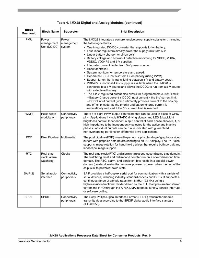
PMU Power management Unit (DC-DC)
Power management system
The i.MX28 integrates a comprehensive power supply subsystem, including the following features:
• One integrated DC-DC converter that supports Li-Ion battery. • Four linear regulators directly power the supply rails from 5-V. • Linear battery charger for Li-Ion cells. • Battery voltage and brownout detection monitoring for VDDD, VDDA,
VDDIO, VDD4P2 and 5-V supplies. • Integrated current limiter from 5-V power source. • Reset controller. • System monitors for temperature and speed. • Generates USB-Host 5-V from Li-Ion battery (using PWM). • Support for on-the-fly transitioning between 5-V and battery power. • VDD4P2, a nominal 4.2-V supply, is available when the i.MX28 is
connected to a 5-V source and allows the DCDC to run from a 5-V source with a depleted battery.
• The 4.2-V regulated output also allows for programmable current limits: – Battery Charge current + DCDC input current < the 5-V current limit – DCDC input current (which ultimately provides current to the on-chip and off-chip loads) as the priority and battery charge current is automatically reduced if the 5-V current limit is reached
PWM(8) Pulse width modulation
Connectivity peripherals
There are eight PWM output controllers that can be used in place of GPIO pins. Applications include HSADC driving signals and LED & backlight brightness control. Independent output control of each phase allows 0, 1, or high-impedance to be independently selected for the active and inactive phases. Individual outputs can be run in lock step with guaranteed non-overlapping portions for differential drive applications.
PXP Pixel Pipeline Multimedia The pixel pipeline (PXP) is used to perform alpha blending of graphic or video buffers with graphics data before sending to an LCD display. The PXP also supports image rotation for hand-held devices that require both portrait and landscape image support.
RTC Real-time clock, alarm, watchdog
Clocks The real-time clock (RTC) and alarm share a one-second pulse time domain. The watchdog reset and millisecond counter run on a one-millisecond time domain. The RTC, alarm, and persistent bits reside in a special power domain (crystal domain) that remains powered up even when the rest of the chip is in its powered-down state.
SAIF(2) Serial audio interface
Connectivity peripherals
SAIF provides a half-duplex serial port for communication with a variety of serial devices, including industry-standard codecs and DSPs. It supports a continuous range of sample rates from 8 kHz–192 kHz using a high-resolution fractional divider driven by the PLL. Samples are transferred to/from the FIFO through the APBX DMA interface, a FIFO service interrupt, or software polling.
SPDIF SPDIF Connectivity peripherals
The Sony-Philips Digital Interface Format (SPDIF) transmitter module transmits data according to the SPDIF digital audio interface standard (IEC-60958).
Table 4. i.MX28 Digital and Analog Modules (continued)
Block Mnemonic
Block Name Subsystem Brief Description
i.MX28 Applications Processor Data Sheet for Consumer Products, Rev. 0
Freescale Semiconductor 9
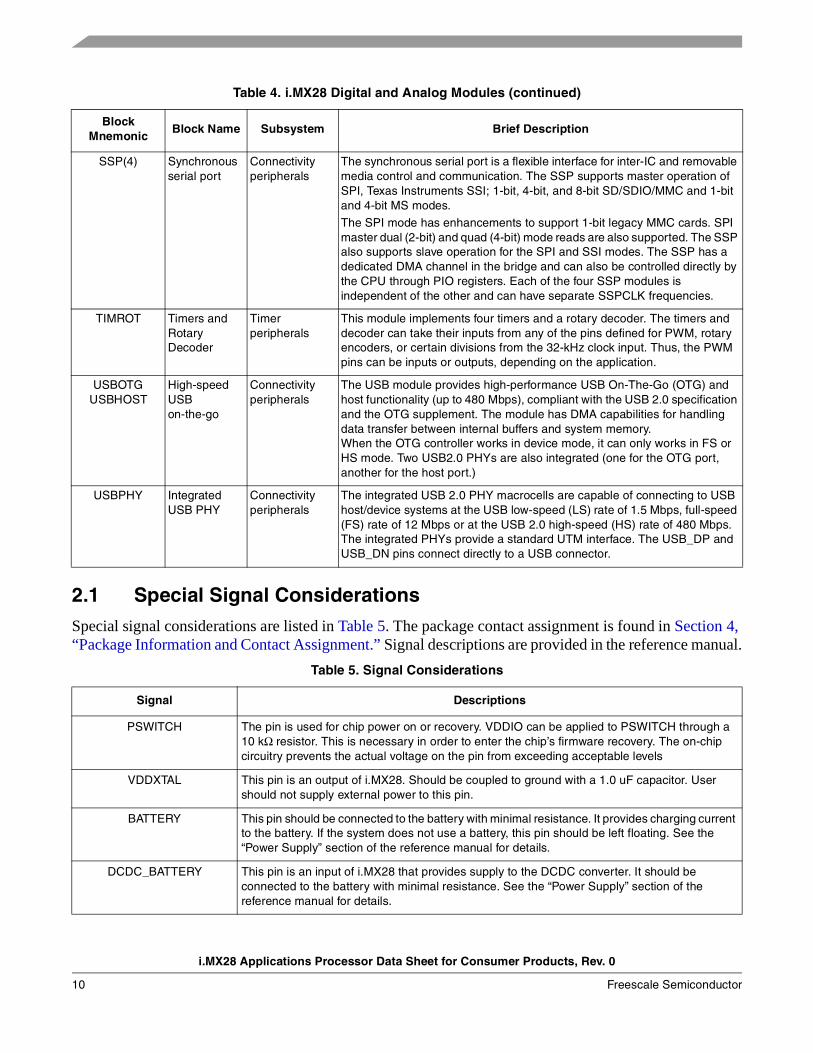
2.1 Special Signal ConsiderationsSpecial signal considerations are listed in Table 5. The package contact assignment is found in Section 4, “Package Information and Contact Assignment.” Signal descriptions are provided in the reference manual.
SSP(4) Synchronous serial port
Connectivity peripherals
The synchronous serial port is a flexible interface for inter-IC and removable media control and communication. The SSP supports master operation of SPI, Texas Instruments SSI; 1-bit, 4-bit, and 8-bit SD/SDIO/MMC and 1-bit and 4-bit MS modes.
The SPI mode has enhancements to support 1-bit legacy MMC cards. SPI master dual (2-bit) and quad (4-bit) mode reads are also supported. The SSP also supports slave operation for the SPI and SSI modes. The SSP has a dedicated DMA channel in the bridge and can also be controlled directly by the CPU through PIO registers. Each of the four SSP modules is independent of the other and can have separate SSPCLK frequencies.
TIMROT Timers and Rotary Decoder
Timer peripherals
This module implements four timers and a rotary decoder. The timers and decoder can take their inputs from any of the pins defined for PWM, rotary encoders, or certain divisions from the 32-kHz clock input. Thus, the PWM pins can be inputs or outputs, depending on the application.
USBOTG USBHOST
High-speed USB on-the-go
Connectivity peripherals
The USB module provides high-performance USB On-The-Go (OTG) and host functionality (up to 480 Mbps), compliant with the USB 2.0 specification and the OTG supplement. The module has DMA capabilities for handling data transfer between internal buffers and system memory. When the OTG controller works in device mode, it can only works in FS or HS mode. Two USB2.0 PHYs are also integrated (one for the OTG port, another for the host port.)
USBPHY Integrated USB PHY
Connectivity peripherals
The integrated USB 2.0 PHY macrocells are capable of connecting to USB host/device systems at the USB low-speed (LS) rate of 1.5 Mbps, full-speed (FS) rate of 12 Mbps or at the USB 2.0 high-speed (HS) rate of 480 Mbps. The integrated PHYs provide a standard UTM interface. The USB_DP and USB_DN pins connect directly to a USB connector.
Table 5. Signal Considerations
Signal Descriptions
PSWITCH The pin is used for chip power on or recovery. VDDIO can be applied to PSWITCH through a 10 kΩ resistor. This is necessary in order to enter the chip’s firmware recovery. The on-chip circuitry prevents the actual voltage on the pin from exceeding acceptable levels
VDDXTAL This pin is an output of i.MX28. Should be coupled to ground with a 1.0 uF capacitor. User should not supply external power to this pin.
BATTERY This pin should be connected to the battery with minimal resistance. It provides charging current to the battery. If the system does not use a battery, this pin should be left floating. See the “Power Supply” section of the reference manual for details.
DCDC_BATTERY This pin is an input of i.MX28 that provides supply to the DCDC converter. It should be connected to the battery with minimal resistance. See the “Power Supply” section of the reference manual for details.
Table 4. i.MX28 Digital and Analog Modules (continued)
Block Mnemonic
Block Name Subsystem Brief Description
i.MX28 Applications Processor Data Sheet for Consumer Products, Rev. 0
10 Freescale Semiconductor
3 Electrical CharacteristicsThis section provides the device-level and module-level electrical characteristics for the i.MX28.
3.1 i.MX28 Device-Level ConditionsThis section provides the device-level electrical characteristics for the IC.
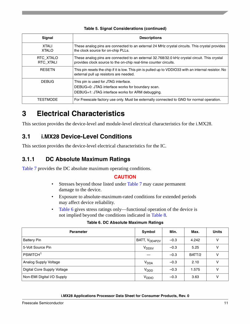
3.1.1 DC Absolute Maximum Ratings
Table 7 provides the DC absolute maximum operating conditions.
CAUTION• Stresses beyond those listed under Table 7 may cause permanent
damage to the device.
• Exposure to absolute-maximum-rated conditions for extended periods may affect device reliability.
• Table 6 gives stress ratings only—functional operation of the device is not implied beyond the conditions indicated in Table 8.
XTALIXTALO
These analog pins are connected to an external 24 MHz crystal circuits. This crystal provides the clock source for on-chip PLLs.
RTC_XTALORTC_XTALI
These analog pins are connected to an external 32.768/32.0 kHz crystal circuit. This crystal provides clock source to the on-chip real-time counter circuits.
RESETN This pin resets the chip if it is low. This pin is pulled up to VDDIO33 with an internal resistor. No external pull up resistors are needed.
DEBUG This pin is used for JTAG interface.
DEBUG=0: JTAG interface works for boundary scan.
DEBUG=1: JTAG interface works for ARM debugging.
TESTMODE For Freescale factory use only. Must be externally connected to GND for normal operation.
Table 6. DC Absolute Maximum Ratings
Parameter Symbol Min. Max. Units
Battery Pin BATT, VDD4P2V –0.3 4.242 V
5-Volt Source Pin VDD5V –0.3 5.25 V
PSWITCH1 — –0.3 BATT/2 V
Analog Supply Voltage VDDA –0.3 2.10 V
Digital Core Supply Voltage VDDD –0.3 1.575 V
Non-EMI Digital I/O Supply VDDIO –0.3 3.63 V
Table 5. Signal Considerations (continued)
Signal Descriptions
i.MX28 Applications Processor Data Sheet for Consumer Products, Rev. 0
Freescale Semiconductor 11

Table 7 shows the electrostatic discharge immunity.
Note that HBM and CDM pass ESD testing per JEDEC spec, JESD22-A114A115.
EMI Digital I/O Supply VDDIO.EMI –0.3 3.63 V
DC-DC Converter2 DCDC_BATT –0.3 BATT V
Input Voltage on Any Digital I/O Pin Relative to Ground — –0.3 VDDIO+0.3 V
Input Voltage on USB_DP and USB_DN Pins Relative to Ground3 — –0.3 3.63 V
Analog I/O absolute maximum ratings (exceptions: XTALI, XTALO, RTC_XTALI, RTC_XTALO)
— –0.3 VDDIO+0.3 V
Storage Temperature — –40 125 °C
1 VDDIO can be applied to PSWITCH through a 10 kΩ resistor. This is necessary in order to enter the chip’s firmware recovery mode. (The on-chip circuitry prevents the actual voltage on the pin from exceeding acceptable levels.)
2 Application should include a Schottky diode between BATT and VDD4P2.3 USB_DN and USB_DP can tolerate 5V for up to 24 hours. Note that while 5V is applied to USB_DN or USB_DP, LRADC
readings can be corrupted.
Table 7. Electrostatic Discharge Immunity
289-Pin BGA Package Tested Level
Human Body Model (HBM) 2 kV
Charge Device Model (CDM) 500 V
Table 6. DC Absolute Maximum Ratings (continued)
Parameter Symbol Min. Max. Units
i.MX28 Applications Processor Data Sheet for Consumer Products, Rev. 0
12 Freescale Semiconductor

3.1.2 DC Operating Conditions
Table 8 provides the DC recommended operating conditions.
Table 9 provides the DC operating temperature conditions.
Table 8. Recommended Power Supply Operating Conditions
Parameter Symbol Min Typ Max Units
Analog Core Supply Voltage VDDA 1.62 — 2.10 V
Digital Core Supply VoltageSpecification dependent on frequency.1, 2
1 For optimum USB jitter performance, VDDD = 1.35 V or greater.2 VDDD supply minimum voltage includes 75 mV guardband.
VDDD 1.25 — 1.55 V
Non-EMI Digital I/O Supply Voltage:
• VDDIO33 • VDDIO18
VDDIO33/VDDIO183.01.7
——
3.61.9
V
EMI Digital I/O Supply Voltage:
• DDR2/mDDR • LVDDR2
VDDIO.EMI/VDDIO_EMIQ1.7
1.4251.81.5
1.91.625
V
Battery / DCDC Input Voltage - BATT, DCDC_BATT BATTDCDC_BATT
3.3 — 4.242 V
VDD5V Supply Voltage (5 V current < 100 mA) — TBD 5.00 5.25 V
VDD5V Supply Voltage (5V current ≥ 100 mA) — 4.75 5.00 5.25 V
Offstate Current:3
3 When the real-time clock is enabled, the chip consumes additional current in the OFF state to keep the crystal oscillator and the real-time clock running.
• 32-kHz RTC off, BATT = 4.2 V — — 11 30 µA
• 32-kHz RTC on, BATT = 4.2 V — — 13.5 30 µA
Table 9. Operating Temperature Conditions
Parameter Symbol Min Typ Max Units
Commercial Ambient Operating Temperature Range1, 2
1 In most portable systems designs, battery and display specifications limits the operating range to well within these specifications. Most battery manufacturers recommend enabling battery charge only when the ambient temperature is between 0° and 40°C. To ensure that battery charging does not occur outside the recommended temperature range, the system ambient temperature may be monitored by connecting a thermistor to the LRADC0 or LRADC6 pin on the i.MX28.
TA –20 — 70 °C
Commercial Junction Temperature Range1, 2 TJ –20 — 85 °C
Industrial Ambient Operating Temperature Range1, 2 TA –40 — 85 °C
Industrial Junction Temperature Range1, 2 TJ –40 — 105 °C
Package Thermal Impedance, 289-ball MAPBGA3 ΘJA — — 42 °C/W
i.MX28 Applications Processor Data Sheet for Consumer Products, Rev. 0
Freescale Semiconductor 13
Table 10 provides the recommended analog operating conditions.
Table 11 shows the PSWITCH input characteristics. See the reference schematics for the recommended PSWITCH button circuitry.
Table 12 shows the DC characteristics.
2 Maximum Ambient Operating Temperature may be limited due to on-chip power dissipation. TA (MAX) ≤ TJ - ( ΘJA x PD ) where:
TJ = Maximum Junction TemperatureΘJA = Package Thermal ImpedancePD = Total On-chip Power Dissipation =PVDD4P2 + PBatteryCharger + PDCDC + PLinearRegulators + PInternal. Depending
on the application, some of these power dissipation terms may not apply.PVDD4P2 = VDD4P2 On-Chip Power Dissipation = (VDD5V - VDD4P2) x IDD4P2PBatteryCharger = Battery Charger On-Chip Power Dissipation = (VDD5V - BATT) x ICHARGEPDCDC = DC-DC Converter On-Chip Power Dissipation = (BATT x DCDC Input Current) x (1 - efficiency)PLinearRegulators = Linear Regulator On-Chip Power Dissipation = (VDD5V - VDDIO) x (IDDIO + IDDA + IDDD + IDD1P5) +
(VDDIO - VDDA) x (IDDA + IDDD) + (VDDA - VDDD) x IDDD + (VDDA - VDD1P5) x IDD1P5PInternal = Internal Digital On-Chip Power Dissipation = ~VDDD x IDDD
3 Assumes 6-layer PCB and still air. Actual thermal performance may vary based on board and enclosure composition and design.
Table 10. Recommended Analog Operating Conditions
Parameter Min Typ Max Units
Low Resolution ADC Input Impedance (CH0 - CH5) >1 — — MΩ
Table 11. PSWITCH Input Characteristics
Parameter HW_PWR_STS_PSWITCH Min Max Units
PSWITCH LOW LEVEL 0x00 0.00 0.30 V
PSWITCH MID LEVEL & STARTUP1
1 A MID LEVEL PSWITCH state can be generated by connecting the VDDXTAL output of the SOC to PSWITCH through a switch.
0x01 0.65 1.50 V
PSWITCH HIGH LEVEL2
2 PSWITCH acts like a high impedance input (>300 kΩ) when the voltage applied to it is less than 1.5V. However, above 1.5V it becomes lower impedance. To simplify design, it is recommended that a 10 kΩ resistor to VDDIO be applied to PSWITCH to set the HIGH LEVEL state (the PSWITCH input can tolerate voltages greater than 2.45 V as long as there is a 10 kΩ resistor in series to limit the current).
0x11 (1.1 * VDDXTAL) + 0.58
2.45 V
Table 12. DC Characteristics
Parameter Min Typ Max Units
Power Dissipation: Conditions - TBD — TBD — mW
i.MX28 Applications Processor Data Sheet for Consumer Products, Rev. 0
14 Freescale Semiconductor
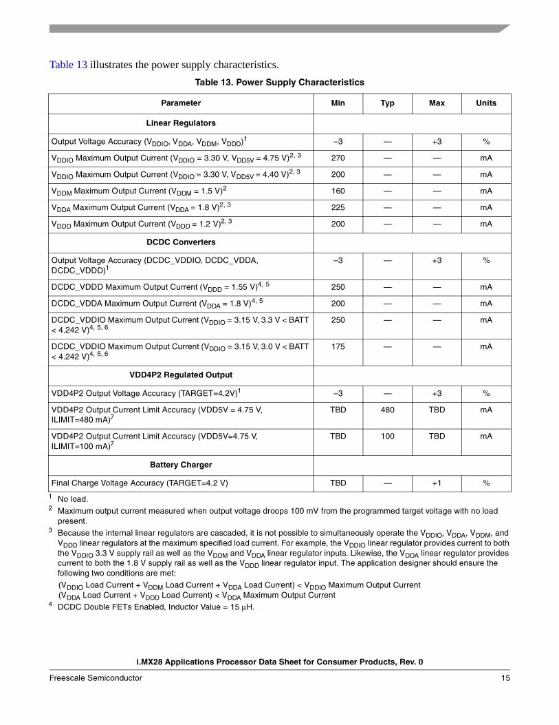
Table 13 illustrates the power supply characteristics.
Table 13. Power Supply Characteristics
Parameter Min Typ Max Units
Linear Regulators
Output Voltage Accuracy (VDDIO, VDDA, VDDM, VDDD)1
1 No load.
–3 — +3 %
VDDIO Maximum Output Current (VDDIO = 3.30 V, VDD5V = 4.75 V)2, 3
2 Maximum output current measured when output voltage droops 100 mV from the programmed target voltage with no load present.
3 Because the internal linear regulators are cascaded, it is not possible to simultaneously operate the VDDIO, VDDA, VDDM, and VDDD linear regulators at the maximum specified load current. For example, the VDDIO linear regulator provides current to both the VDDIO 3.3 V supply rail as well as the VDDM and VDDA linear regulator inputs. Likewise, the VDDA linear regulator provides current to both the 1.8 V supply rail as well as the VDDD linear regulator input. The application designer should ensure the following two conditions are met:
(VDDIO Load Current + VDDM Load Current + VDDA Load Current) < VDDIO Maximum Output Current (VDDA Load Current + VDDD Load Current) < VDDA Maximum Output Current
270 — — mA
VDDIO Maximum Output Current (VDDIO = 3.30 V, VDD5V = 4.40 V)2, 3 200 — — mA
VDDM Maximum Output Current (VDDM = 1.5 V)2 160 — — mA
VDDA Maximum Output Current (VDDA = 1.8 V)2, 3 225 — — mA
VDDD Maximum Output Current (VDDD = 1.2 V)2, 3 200 — — mA
DCDC Converters
Output Voltage Accuracy (DCDC_VDDIO, DCDC_VDDA, DCDC_VDDD)1
–3 — +3 %
DCDC_VDDD Maximum Output Current (VDDD = 1.55 V)4, 5
4 DCDC Double FETs Enabled, Inductor Value = 15 μH.
250 — — mA
DCDC_VDDA Maximum Output Current (VDDA = 1.8 V)4, 5 200 — — mA
DCDC_VDDIO Maximum Output Current (VDDIO = 3.15 V, 3.3 V < BATT < 4.242 V)4, 5, 6
250 — — mA
DCDC_VDDIO Maximum Output Current (VDDIO = 3.15 V, 3.0 V < BATT < 4.242 V)4, 5, 6
175 — — mA
VDD4P2 Regulated Output
VDD4P2 Output Voltage Accuracy (TARGET=4.2V)1 –3 — +3 %
VDD4P2 Output Current Limit Accuracy (VDD5V = 4.75 V, ILIMIT=480 mA)7
TBD 480 TBD mA
VDD4P2 Output Current Limit Accuracy (VDD5V=4.75 V, ILIMIT=100 mA)7
TBD 100 TBD mA
Battery Charger
Final Charge Voltage Accuracy (TARGET=4.2 V) TBD — +1 %
i.MX28 Applications Processor Data Sheet for Consumer Products, Rev. 0
Freescale Semiconductor 15

3.1.2.1 Recommended Operating Conditions for Specific Clock Targets
Table 14 through Table 18 provide the recommended operating conditions for specific clock targets.
5 The DCDC Converter is a triple output buck converter. The maximum output current capability of each output of the converter is dependent on the loads on the other two outputs. For a given output, it may be possible to achieve a maximum output current higher than that specified by ensuring the load on the other outputs is well below the maximum.
6 Assumes simultaneous load of IDDD = 250 mA@ 1.55 V and IDDA = 200 [email protected] V.7 Untuned.
Table 14. System Clocks
Name Min. Freq. (MHz) Max. Freq. (MHz) Description
clk_gpmi — TBD General purpose memory interface clock domain
clk_ssp — TBD SSP interface clock domain
Table 15. Recommended Operating States—289-Pin BGA Package
VDDD(V)
VDDDBrown-out
(V)
HW_DIGCTRL
ARMCACHE1
1 All timing control bit fields in HW_DIGCTRL_ARMCACHE should be set to the same value.
CPUCLK / clk_p
Frequency(MHz)
HW_CLKCTRL
CPU_DIV_CPU
HW_CLKCTRL
FRAC_CPUFRC
/ PFD
AHBCLK/ clk_h
Frequency(MHz)
HW_CLKCTRL
HBUS_DIV
EMICLK/ clk_emi
Frequency(MHz)
HW_CLKCTRL
EMI_DIV_EMI
HW_CLKCTRL
FRAC_EMIFRAC
SupportedDRAM
TBD TBD 00 64 5 27 64 1 130.91 2 33 DDR2mDDR
1.350 1.250 00 261.81 1 33 130.91 2 130.91 2 33 DDR2mDDR
1.350 1.250 00 360 1 21 120.00 3 130.91 2 33 DDR2mDDR
1.450 1.350 00 TBD 1 22 TBD 3 160.00 2 27 DDR2mDDR
1.550 1.450 00 454.73 1 19 151.57 3 205.71 2 29 DDR2
1.550 1.450 00 454.73 1 19 151.57 3 205.71 2 21 mDDR
Table 16. Recommended Operating Conditions—CPU Clock (clk_p)
MinimumVDDD (V)
MinimumVDDDBrown-out (V)
HW_DIGCTRL ARMCACHE1
1 All timing control bit fields in HW_DIGCTRL_ARMCACHE should be set to the same value.
HW_CLKCTRL FRAC_CPUFRC / PFD
CPUCLK / clk_p Frequency max (MHz)
TBD TBD 00 27 - 35 TBD
1.350 1.250 00 18 - 35 TBD
1.450 1.350 00 18 - 35 TBD
1.550 1.450 00 18 - 35 TBD
i.MX28 Applications Processor Data Sheet for Consumer Products, Rev. 0
16 Freescale Semiconductor
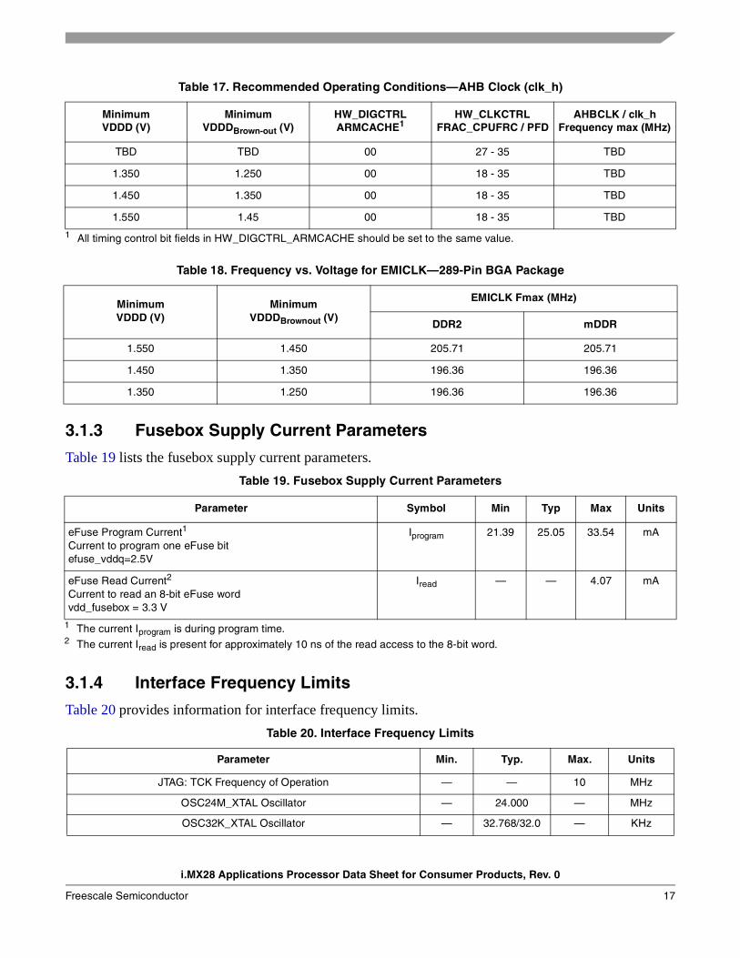
3.1.3 Fusebox Supply Current Parameters
Table 19 lists the fusebox supply current parameters.
3.1.4 Interface Frequency Limits
Table 20 provides information for interface frequency limits.
Table 17. Recommended Operating Conditions—AHB Clock (clk_h)
MinimumVDDD (V)
MinimumVDDDBrown-out (V)
HW_DIGCTRL ARMCACHE1
1 All timing control bit fields in HW_DIGCTRL_ARMCACHE should be set to the same value.
HW_CLKCTRL FRAC_CPUFRC / PFD
AHBCLK / clk_h Frequency max (MHz)
TBD TBD 00 27 - 35 TBD
1.350 1.250 00 18 - 35 TBD
1.450 1.350 00 18 - 35 TBD
1.550 1.45 00 18 - 35 TBD
Table 18. Frequency vs. Voltage for EMICLK—289-Pin BGA Package
MinimumVDDD (V)
MinimumVDDDBrownout (V)
EMICLK Fmax (MHz)
DDR2 mDDR
1.550 1.450 205.71 205.71
1.450 1.350 196.36 196.36
1.350 1.250 196.36 196.36
Table 19. Fusebox Supply Current Parameters
Parameter Symbol Min Typ Max Units
eFuse Program Current1
Current to program one eFuse bitefuse_vddq=2.5V
1 The current Iprogram is during program time.
Iprogram 21.39 25.05 33.54 mA
eFuse Read Current2
Current to read an 8-bit eFuse wordvdd_fusebox = 3.3 V
2 The current Iread is present for approximately 10 ns of the read access to the 8-bit word.
Iread — — 4.07 mA
Table 20. Interface Frequency Limits
Parameter Min. Typ. Max. Units
JTAG: TCK Frequency of Operation — — 10 MHz
OSC24M_XTAL Oscillator — 24.000 — MHz
OSC32K_XTAL Oscillator — 32.768/32.0 — KHz
i.MX28 Applications Processor Data Sheet for Consumer Products, Rev. 0
Freescale Semiconductor 17
3.1.5 Power ModesTable 21 describes the core, clock, and module settings for the different power modes of the processor.
3.1.6 Supply Power-Up/Power-Down RequirementsThere is no special power-up sequence. After applying 5 V or battery in any order, the rest of the power supplies are internally generated and automatically come up in a safe way.
There is no special power-down sequence. 5 V or the battery can be removed at any time.
3.1.7 Reset TimingBecause the i.MX28 is a PMU and an SoC, power-on reset is generated internally and there is no timing requirement on external pins.
The i.MX28 can be reset by asserting the exernal pin RESETN for at least 100 mS and later deasserting RESETN.
If the reset occurs while the device only powered by the battery, then the reset kills all of the power supplies; and the system reboots on the assertion of PSWITCH, or immediately if auto-restart is set up ahead of time.
If the chip is powered by 5 V, then the reset serves to reset the digital sections of the chip. If the DCDC is operating at the time of the reset, then power switches back to the default linear regulators powered by 5 V.
Table 21. Power Mode Settings
Core/Clock/Module Deep-Sleep Standby Run (300 MHz) Run (454 MHz)
ARM Core Off Off Active@300 MHz Active@454 MHz
USB0 PLL (System PLL) Off Off On On
OSC24M Off On On On
OSC32K On On On On
DCDC Off On On On
RTC On On On On
Other Modules Off Off On On
Powered by battery (mA) TYP 13.5uA TBD TBD TBD
MAX 30uA TBD TBD TBD
Powered by 5 V (mA) TYP TBD TBD TBD TBD
MAX TBD TBD TBD TBD
i.MX28 Applications Processor Data Sheet for Consumer Products, Rev. 0
18 Freescale Semiconductor
Figure 2. RESETN Timing
3.2 I/O DC ParametersThis section includes the DC parameters of the following I/O types:
• DDR I/O: Mobile DDR (LPDDR1), standard 1.8 V DDR2, and low-voltage 1.5 V DDR2 (LVDDR2)
• General purpose I/O (GPIO)
3.2.1 DDR I/O DC Parameters
Table 22 shows the EMI digital pin DC characteristics.
NOTEThe current values and the I-V curves of the I/O DC characteristics are estimated based on an overly conservative device model. They are updated upon the measurement results of the first silicon.
Table 22. EMI Digital Pin DC Characteristics
Parameter Symbol Min. Max. Units
Core supply voltage VDDD 1.250 1.550 V
3.3V I/O supply voltage VDDIO33 / VDDIO33_EMI
3 3.6 V
I/O Voltage (LVDDR2 Mode) VDDIO_EMI / VDDIO_EMIQ
1.425 1.575 V
I/O Voltage (mDDR Mode, DDR2 Mode)
VDDIO_EMI 1.7 1.9 V
Input voltage high (dc) VIH VREF + 0.125 VDDIO_EMI + 0.3 V
Input voltage low (dc) VIL 0.3 VREF – 0.125 V
Output voltage high (dc) VOH 0.8 * VDDIO_EMI — V
Output voltage low (dc) VOL - 0.2 * VDDIO_EMI V
Output source current (dc)LVDDR2 Mode
IOH1—Low TBD TBD mA
IOH—Medium TBD TBD mA
IOH—High TBD TBD mA
RESETN
At lease 100ms
i.MX28 Applications Processor Data Sheet for Consumer Products, Rev. 0
Freescale Semiconductor 19
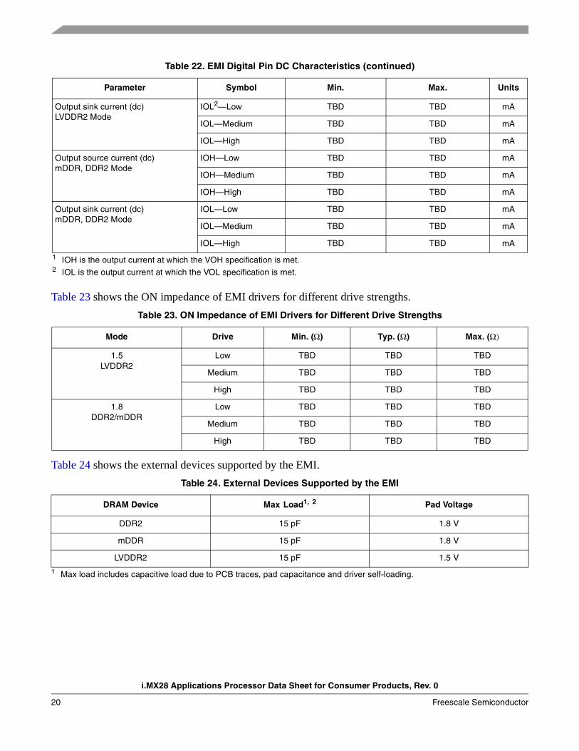
Table 23 shows the ON impedance of EMI drivers for different drive strengths.
Table 24 shows the external devices supported by the EMI.
Output sink current (dc)LVDDR2 Mode
IOL2—Low TBD TBD mA
IOL—Medium TBD TBD mA
IOL—High TBD TBD mA
Output source current (dc)mDDR, DDR2 Mode
IOH—Low TBD TBD mA
IOH—Medium TBD TBD mA
IOH—High TBD TBD mA
Output sink current (dc)mDDR, DDR2 Mode
IOL—Low TBD TBD mA
IOL—Medium TBD TBD mA
IOL—High TBD TBD mA
1 IOH is the output current at which the VOH specification is met. 2 IOL is the output current at which the VOL specification is met.
Table 23. ON Impedance of EMI Drivers for Different Drive Strengths
Mode Drive Min. (Ω) Typ. (Ω) Max. (Ω)
1.5LVDDR2
Low TBD TBD TBD
Medium TBD TBD TBD
High TBD TBD TBD
1.8DDR2/mDDR
Low TBD TBD TBD
Medium TBD TBD TBD
High TBD TBD TBD
Table 24. External Devices Supported by the EMI
DRAM Device Max Load1, 2
1 Max load includes capacitive load due to PCB traces, pad capacitance and driver self-loading.
Pad Voltage
DDR2 15 pF 1.8 V
mDDR 15 pF 1.8 V
LVDDR2 15 pF 1.5 V
Table 22. EMI Digital Pin DC Characteristics (continued)
Parameter Symbol Min. Max. Units
i.MX28 Applications Processor Data Sheet for Consumer Products, Rev. 0
20 Freescale Semiconductor

3.2.2 GPIO I/O DC ParametersMax load includes capacitive load due to PCB traces, pad capacitance and driver self-loading. For the internal pull.up setting of each pad, see the “Pin Control and GPIO” section of the reference manual.
Table 25 shows the digital pin DC characteristics for GPIO in 3.3-V mode. Measurements are valid for 8 pins loaded using the 4mA driver, 4 pins loaded using the 8mA driver, and 2 pins loaded using either the 12mA or 16mA driver.
2 Setting is for worst case. Freescale’s EMI interface uses less powerful drivers than those typically used in mDDR devices. A possible transmission-line effect on the PC board must be suppressed by minimizing the trace length combined with Freescale’s slower edge-rate drivers. The i.MX28 provides up to 16 mA programmable drive strength. However, the 16-mA mode is an experimental mode. With the 16-mA mode, the EMI function may be impaired by Simultaneous Switching Output (SSO) noise. In general, the stronger the driver mode, the noisier the on-chip power supply. Freescale recommends not using a stronger driver mode than is required. Because on-chip power and ground noise is proportional to the inductance of its return path, users should make their best effort to reduce inductance between the EMI power and ground balls and the PC board power and ground planes.
Table 25. Digital Pin DC Characteristics for GPIO in 3.3-V Mode
Parameter Symbol Min Max Units
Core supply voltage VDDD 1.25 1.55 V
3.3V I/O supply voltage VDDIO33 3 3.6 V
Input voltage high (dc) VIH 2 VDDIO V
Input voltage low (dc) VIL — 0.8 V
Output voltage high (dc) VOH 0.8 × VDDIO — V
Output voltage low (dc) VOL — 0.4 V
Output source current1 (dc)gpio, gpio_f, and gpio_nobs
IOH – 4mA 3.8 6.8 mA
IOH – 8mA 7.6 13.6 mA
IOH – 12mA 11.4 20.4 mA
Output sink current1 (dc)gpio, gpio_f, and gpio_nobs
IOL – 4mA 4 8.1 mA
IOL – 8mA 8.1 16.4 mA
IOL – 12mA 12.1 24.5 mA
Output source current1 (dc)gpio_clk
IOH – 8mA 7.6 13.6 mA
IOH – 16mA 15.2 27.2 mA
Output sink current1 (dc)gpio_clk
IOL – 8mA 8.1 15.4 mA
IOL – 16mA 16.2 30.9 mA
10-K pull-up resistance2 Rpu10k 8 12 KΩ
47-K pull-up resistance2 Rpu47k 39 56 KΩ
i.MX28 Applications Processor Data Sheet for Consumer Products, Rev. 0
Freescale Semiconductor 21
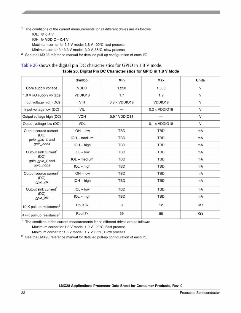
Table 26 shows the digital pin DC characteristics for GPIO in 1.8 V mode.
1 The conditions of the current measurements for all different drives are as follows:
IOL: @ 0.4 V
IOH: @ VDDIO – 0.4 V
Maximum corner for 3.3 V mode: 3.6 V, -20°C, fast process.
Minimum corner for 3.3 V mode: 3.0 V, 85°C, slow process2 See the i.MX28 reference manual for detailed pull-up configuration of each I/O.
Table 26. Digital Pin DC Characteristics for GPIO in 1.8 V Mode
Symbol Min Max Units
Core supply voltage VDDD 1.250 1.550 V
1.8 V I/O supply voltage VDDIO18 1.7 1.9 V
Input voltage high (DC) VIH 0.8 × VDDIO18 VDDIO18 V
Input voltage low (DC) VIL — 0.2 × VDDIO18 V
Output voltage high (DC) VOH 0.9 * VDDIO18 — V
Output voltage low (DC) VOL — 0.1 × VDDIO18 V
Output source current1 (DC)
gpio, gpio_f, and gpio_nobs
1 The condition of the current measurements for all different drives are as follows:
Maximum corner for 1.8 V mode: 1.9 V, -20°C, Fast process.
Minimum corner for 1.8 V mode: 1.7 V, 85°C, Slow process
IOH – low TBD TBD mA
IOH – medium TBD TBD mA
IOH – high TBD TBD mA
Output sink current1 (DC)
gpio, gpio_f, and gpio_nobs
IOL – low TBD TBD mA
IOL – medium TBD TBD mA
IOL – high TBD TBD mA
Output source current1 (DC)
gpio_clk
IOH – low TBD TBD mA
IOH – high TBD TBD mA
Output sink current1 (DC)
gpio_clk
IOL – low TBD TBD mA
IOL – high TBD TBD mA
10-K pull-up resistance2
2 See the i.MX28 reference manual for detailed pull-up configuration of each I/O.
Rpu10k 8 12 KΩ
47-K pull-up resistance2 Rpu47k 39 56 KΩ
i.MX28 Applications Processor Data Sheet for Consumer Products, Rev. 0
22 Freescale Semiconductor
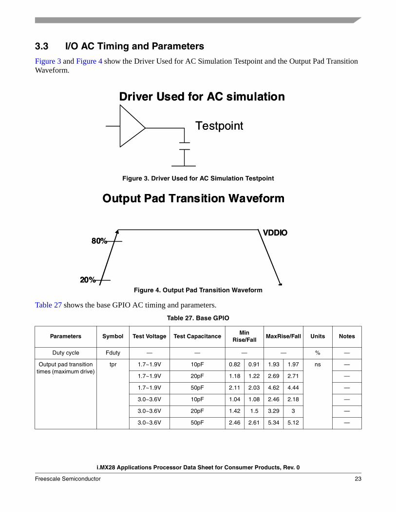
3.3 I/O AC Timing and ParametersFigure 3 and Figure 4 show the Driver Used for AC Simulation Testpoint and the Output Pad Transition Waveform.
Figure 3. Driver Used for AC Simulation Testpoint
Figure 4. Output Pad Transition Waveform
Table 27 shows the base GPIO AC timing and parameters.
Table 27. Base GPIO
Parameters Symbol Test Voltage Test CapacitanceMin
Rise/FallMaxRise/Fall Units Notes
Duty cycle Fduty — — — — % —
Output pad transition times (maximum drive)
tpr 1.7~1.9V 10pF 0.82 0.91 1.93 1.97 ns —
1.7~1.9V 20pF 1.18 1.22 2.69 2.71 —
1.7~1.9V 50pF 2.11 2.03 4.62 4.44 —
3.0~3.6V 10pF 1.04 1.08 2.46 2.18 —
3.0~3.6V 20pF 1.42 1.5 3.29 3 —
3.0~3.6V 50pF 2.46 2.61 5.34 5.12 —
Driver Used for AC simulation
Testpoint
Driver Used for AC simulation
Testpoint
Output Pad Transition Waveform
VDDIO
20%
80%
Output Pad Transition Waveform
VDDIO
20%
80%
i.MX28 Applications Processor Data Sheet for Consumer Products, Rev. 0
Freescale Semiconductor 23

Output pad transition times (medium drive)
tpr 1.7~1.9V 10pF 1.02 1.08 2.34 2.38 ns —
1.7~1.9V 20pF 1.51 1.5 3.34 3.28 —
1.7~1.9V 50pF 2.91 2.62 6.24 5.67 —
3.0~3.6V 10pF 1.26 1.29 2.9 2.6 —
3.0~3.6V 20pF 1.8 1.88 4 3.67 —
3.0~3.6V 50pF 3.3 3.46 6.91 6.64 —
Output pad transition times (low drive)
tpr 1.7~1.9V 10pF 1.62 1.68 3.65 3.68 ns —
1.7~1.9V 20pF 2.55 2.45 5.59 5.37 —
1.7~1.9V 50pF 5.42 4.62 11.46 10.01 —
3.0~3.6V 10pF 1.95 2.12 4.43 4.25 —
3.0~3.6V 20pF 2.96 3.21 6.36 6.25 —
3.0~3.6V 50pF 5.89 6.39 12.02 12.18 —
Output pad slew rate (maximum drive)
tps 1.7~1.9V 10pF 1.39 1.25 0.53 0.52 V/ns —
1.7~1.9V 20pF 0.97 0.93 0.38 0.38 —
1.7~1.9V 50pF 0.54 0.56 0.22 0.23 —
3.0~3.6V 10pF 2.08 2.00 0.73 0.83 —
3.0~3.6V 20pF 1.52 1.44 0.55 0.60 —
3.0~3.6V 50pF 0.88 0.83 0.34 0.35 —
Output pad slew rate (medium drive)
tps 1.7~1.9V 10pF 1.12 1.06 0.44 0.43 V/ns —
1.7~1.9V 20pF 0.75 0.76 0.31 0.31 —
1.7~1.9V 50pF 0.39 0.44 0.16 0.18 —
3.0~3.6V 10pF 1.71 1.67 0.62 0.69 —
3.0~3.6V 20pF 1.20 1.15 0.45 0.49 —
3.0~3.6V 50pF 0.65 0.62 0.26 0.27 —
Output pad slew rate (low drive)
tps 1.7~1.9V 10pF 1.17 1.13 0.47 0.46 V/ns —
1.7~1.9V 20pF 0.75 0.78 0.30 0.32 —
1.7~1.9V 50pF 0.35 0.41 0.15 0.17 —
3.0~3.6V 10pF 1.11 1.02 0.41 0.42 —
3.0~3.6V 20pF 0.73 0.67 0.28 0.29 —
3.0~3.6V 50pF 0.37 0.34 0.15 0.15 —
Input pad average hysteresis
tih 1.7 V–1.9 V — 100 75 mV —
3.0 V–3.6 V — 100 50 —
Table 27. Base GPIO (continued)
Parameters Symbol Test Voltage Test CapacitanceMin
Rise/FallMaxRise/Fall Units Notes
i.MX28 Applications Processor Data Sheet for Consumer Products, Rev. 0
24 Freescale Semiconductor

Table 28 shows the F-type GPIO AC timing and parameters.
Table 28. F-type GPIO
Parameters Symbol Test Voltage Test Capacitance Min Rise/Fall Max Rise/Fall Units Notes
Duty cycle Fduty — — — — % —
Output pad transition times (maximum
drive)
tpr 1.7~1.9V 10pF 0.58 0.61 1.29 1.33 ns —
1.7~1.9V 20pF 0.89 0.88 1.94 1.88 —
1.7~1.9V 50pF 1.83 1.59 3.88 3.39 —
3.0~3.6V 10pF 0.71 0.68 1.47 1.34 —
3.0~3.6V 20pF 1.02 1.04 2.11 1.99 —
3.0~3.6V 50pF 1.98 2.09 3.97 3.96 —
Output pad transition times (medium drive)
tpr 1.7~1.9V 10pF 0.76 0.76 1.68 1.61 ns —
1.7~1.9V 20pF 1.23 1.13 2.63 2.38 —
1.7~1.9V 50pF 2.66 2.18 5.61 4.6 —
3.0~3.6V 10pF 0.9 0.88 1.84 1.7 —
3.0~3.6V 20pF 1.36 1.4 2.76 2.67 —
3.0~3.6V 50pF 2.85 3.02 5.59 5.67 —
Output pad transition times (low drive)
tpr 1.7~1.9V 10pF 1.32 1.26 2.88 2.72 ns —
1.7~1.9V 20pF 2.27 1.98 4.84 4.23 —
1.7~1.9V 50pF 5.23 4.13 10.95 8.8 —
3.0~3.6V 10pF 1.46 1.55 3.05 3 —
3.0~3.6V 20pF 2.46 2.62 4.92 5.02 —
3.0~3.6V 50pF 5.56 5.96 10.78 11.22 —
Output pad slew rate (maximum drive)
tps 1.7~1.9V 10pF 1.97 1.87 0.79 0.77 ns —
1.7~1.9V 20pF 1.28 1.30 0.53 0.54 —
1.7~1.9V 50pF 0.62 0.72 0.26 0.30 —
3.0~3.6V 10pF 3.04 3.18 1.22 1.34 —
3.0~3.6V 20pF 2.12 2.08 0.85 0.90 —
3.0~3.6V 50pF 1.09 1.03 0.45 0.45 —
Output pad slew rate (medium drive)
tps 1.7~1.9V 10pF 1.50 1.50 0.61 0.63 ns —1.7~1.9V 20pF 0.93 1.01 0.39 0.43 —
1.7~1.9V 50pF 0.43 0.52 0.18 0.22 —
3.0~3.6V 10pF 2.40 2.45 0.98 1.06 —
3.0~3.6V 20pF 1.59 1.54 0.65 0.67 —
3.0~3.6V 50pF 0.76 0.72 0.32 0.32 —
i.MX28 Applications Processor Data Sheet for Consumer Products, Rev. 0
Freescale Semiconductor 25

Table 29 shows the CLK-type GPIO AC timing and parameters.
Output pad slew rate (low drive)
tps 1.7~1.9V 10pF 1.44 1.51 0.59 0.63 ns —1.7~1.9V 20pF 0.84 0.96 0.35 0.40 —
1.7~1.9V 50pF 0.36 0.46 0.16 0.19 —
3.0~3.6V 10pF 1.48 1.39 0.59 0.60 —
3.0~3.6V 20pF 0.88 0.82 0.37 0.36 —
3.0~3.6V 50pF 0.39 0.36 0.17 0.16 —
Input pad average hysteresis
tih 1.7 V–1.9 V — 100 75 mV —
3.0 V–3.6 V — 100 50 —
Table 29. CLK-Type GPIO
Parameters Symbol Test Voltage Test Capacitance Min Rise/Fall Max Rise/Fall units Notes
Duty cycle Fduty — — — — % —
Output pad transition times (maximum
drive)
tpr 1.7~1.9V 10pF 0.48 0.52 1.08 1.12 ns —
1.7~1.9V 20pF 0.72 0.74 1.56 1.56 —
1.7~1.9V 50pF 1.41 1.28 3.04 2.7 —
3.0~3.6V 10pF 0.61 0.57 1.25 1.12 —
3.0~3.6V 20pF 0.85 0.85 1.73 1.63 —
3.0~3.6V 50pF 1.56 1.63 3.13 3.08 —
Output pad transition times (medium drive)
tpr 1.7~1.9V 10pF 0.76 0.76 1.67 1.62 ns —
1.7~1.9V 20pF 1.22 1.14 2.64 2.41 —
1.7~1.9V 50pF 2.66 2.2 5.61 4.62 —
3.0~3.6V 10pF 0.9 0.89 1.83 1.72 —
3.0~3.6V 20pF 1.37 1.41 2.77 2.69 —
3.0~3.6V 50pF 2.85 3.03 5.59 5.72 —
Output pad slew rate (maximum drive)
tps 1.7~1.9V 10pF 2.38 2.19 0.94 0.91 ns —
1.7~1.9V 20pF 1.58 1.54 0.65 0.65 —
1.7~1.9V 50pF 0.81 0.89 0.34 0.38 —
3.0~3.6V 10pF 3.54 3.79 1.44 1.61 —
3.0~3.6V 20pF 2.54 2.54 1.04 1.10 —
3.0~3.6V 50pF 1.38 1.33 0.58 0.58 —
Table 28. F-type GPIO (continued)
Parameters Symbol Test Voltage Test Capacitance Min Rise/Fall Max Rise/Fall Units Notes
i.MX28 Applications Processor Data Sheet for Consumer Products, Rev. 0
26 Freescale Semiconductor
3.4 Module Timing and Electrical Parameters
3.4.1 ADC Electrical SpecificationsThis section describes the electrical specifications, including DC and AC information, of Low-Resolution ADC (LRADC) and High-Speed ADC (HSADC).
3.4.1.1 LRADC Electrical Specifications
Table 30 shows the electrical specifications for the LRADC.
Output pad slew rate (medium drive)
tps 1.7~1.9V 10pF 1.50 1.50 0.61 0.63 ns —
1.7~1.9V 20pF 0.93 1.00 0.39 0.42 —
1.7~1.9V 50pF 0.43 0.52 0.18 0.22 —
3.0~3.6V 10pF 2.40 2.43 0.98 1.05 —
3.0~3.6V 20pF 1.58 1.53 0.65 0.67 —
3.0~3.6V 50pF 0.76 0.71 0.32 0.31 —
Input pad average hysteresis
tih 1.7 V–1.9 V — 100 75 mV —
3.0 V–3.6 V — 100 50 —
Table 30. LRADC Electrical Specifications
Parameter Conditions Min. Typ. Max. Unit
AC Electrical Specification
Input capacitance (Cp) No pin/pad capacitance included — 0.5 — pF
Resolution — 12 bits
Maximum sampling rate1 (fs)
1 There is no sample and hold circuit in LRADC, so it is only for DC input voltage or ones with very small slope.
— — — 428 kHz
Power-up time2 — 1 sample cycles
DC Electrical Specification
DC input voltage 0 1.85 V
Current consumption3
VDDA
VDDD
— — TBD — mAmA
Touchscreen Interface
Expected plate resistance — 200 — 50000 Ω
Table 29. CLK-Type GPIO (continued)
Parameters Symbol Test Voltage Test Capacitance Min Rise/Fall Max Rise/Fall units Notes
i.MX28 Applications Processor Data Sheet for Consumer Products, Rev. 0
Freescale Semiconductor 27
3.4.1.2 HSADC Electrical Specification
Table 31 shows the electrical specifications for the HSADC
3.4.2 DPLL Electrical SpecificationsThis section includes descriptions of the USB PLL electrical specifications and Ethernet PLL electrical specifications.
3.4.2.1 USB PLL Electrical Specifications
i.MX28 integrates a high-frequency USB PLL that provides the 480-MHz clock for the USB and other system blocks.
Table 32 lists the USB PLL output electrical specifications.
2 This comprises only the required initial dummy conversion cycle, NOT including the Analog part power-up time. 3 This value only includes the ADC and the driver switches, but it does not take into account the current consumption in the
touchscreen plate. For example, if the plate resistance is 200 ohm, the total current consumption is about 11 mA.
Table 31. HSADC Electrical Specification
Parameter Conditions Min. Typ. Max. Unit
AC Electrical Specification
Input sampling capacitance (Cs)
No pin/pad capacitance included — 0.5 — pF
Resolution — 12 bits
Maximum sampling rate (fs)
— — — 2 MHz
Power-up time — 1 sample cycles
DC Electrical Specification
DC input voltage — 0.5 — VDDA-0.5 V
Current ConsumptionVDDAVDDD
— — TBD — mAmA
DNL fin = 1 kHz — — TBD LSB
INL fin = 1kHz — — TBD LSB
Table 32. USB PLL Specifications
Parameter Test Conditions Min Typ Max Unit
PLL lock time — — — 10 µs
i.MX28 Applications Processor Data Sheet for Consumer Products, Rev. 0
28 Freescale Semiconductor
3.4.2.2 Ethernet PLL Electrical Specifications
i.MX28 provides a 50-MHz/25-MHz output clock, called the Ethernet PLL output.
Table 33 lists the Ethernet PLL output electrical specifications.
3.4.3 EMI AC TimingThis section includes descriptions of the electrical specifications of EMI module which interfaces external DDR2 and Mobile-DDR1 (LP-DDR1) memory devices.
Table 33. Ethernet PLL Specifications
Parameter Test Conditions Min Typ Max Unit
Output Duty Cycle — 45 50 55 %
PLL lock time — — — 10 µs
Cycle to cycle jitter — — — TBD ps
i.MX28 Applications Processor Data Sheet for Consumer Products, Rev. 0
Freescale Semiconductor 29

3.4.3.1 EMI Command & Address AC Timing
Figure 5 and Table 34 specify the timing related to the address and command pins that interfaces DDR2 and Mobile-DDR1 memory devices.
Figure 5. EMI Command/Address AC Timing
Table 34. EMI Command/Address AC Timing
ID Description Symbol Min. Max. Unit
DDR1 CK cycle time tCK 6 — ns
DDR2 CK high level widthtCH 0.5 tCK
–0.50.5 tCK+ 0.5
ns
DDR3 CK low level widthtCL 0.5 tCK
–0.50.5 tCK+ 0.5
ns
EMI_CLK
EMI_CLKN
EMI_CE0N
EMI_RASN
EMI_CASN
EMI_WEN
bankrow
bankcolumn
EMI_ADDR
DDR1
DDR2 DDR3
DDR4 DDR5
DDR4 DDR5
DDR4
DDR5
i.MX28 Applications Processor Data Sheet for Consumer Products, Rev. 0
30 Freescale Semiconductor

3.4.3.2 DDR Output AC Timing
Figure 6 and Table 35 show the DDR output AC timing defined for all DDR types: LPDDR1, standard DDR2 (1.8 V), and LVDDR2 (1.5 V)
Figure 6. DDR Output AC Timing
DDR4 Address and control output setup timetIS 0.5 tCK – 1 0.5 tCK
+ 0.5ns
DDR5 Address and control output hold timetIH 0.5 tCK – 1 0.5 tCK
+ 0.5ns
Table 35. DDR Output AC Timing
ID Description Symbol Min Max Unit
DDR10 Positive DQS latching edge to associated CK edge tDQSS –0.5 0.5 ns
DDR11 DQS falling edge from CK rising edge—hold time tDSH 0.5 tCK
–0.5
0.5 tCK
+ 0.5
ns
DDR12 DQS falling edge to CK rising edge—setup time tDSS 0.5 tCK
–0.5
0.5 tCK
+ 0.5
ns
DDR13 DQS output high pulse width tDQSH 0.5 tCK
–0.5
0.5 tCK
+ 0.5
ns
Table 34. EMI Command/Address AC Timing (continued)
ID Description Symbol Min. Max. Unit
EMI_CLK
EMI_CLKN
EMI_DQS
DDR13 DDR14
d0
DDR10
d1 d2 d3EMI_DQ & EMI_DQM
DDR11 DDR12
DDR15
DDR16
EMI_DQSN
i.MX28 Applications Processor Data Sheet for Consumer Products, Rev. 0
Freescale Semiconductor 31
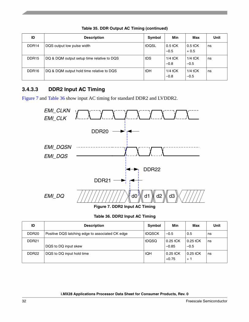
3.4.3.3 DDR2 Input AC Timing
Figure 7 and Table 36 show input AC timing for standard DDR2 and LVDDR2.
Figure 7. DDR2 Input AC Timing
DDR14 DQS output low pulse width tDQSL 0.5 tCK
–0.5
0.5 tCK
+ 0.5
ns
DDR15 DQ & DQM output setup time relative to DQS tDS 1/4 tCK
–0.8
1/4 tCK
–0.5
ns
DDR16 DQ & DQM output hold time relative to DQS tDH 1/4 tCK
–0.8
1/4 tCK
–0.5
ns
Table 36. DDR2 Input AC Timing
ID Description Symbol Min Max Unit
DDR20 Positive DQS latching edge to associated CK edge tDQSCK –0.5 0.5 ns
DDR21
DQS to DQ input skew
tDQSQ 0.25 tCK
–0.85
0.25 tCK
–0.5
ns
DDR22 DQS to DQ input hold time tQH 0.25 tCK
+0.75
0.25 tCK
+ 1
ns
Table 35. DDR Output AC Timing (continued)
ID Description Symbol Min Max Unit
EMI_CLK
EMI_CLKN
EMI_DQS
DDR21
DDR22
d0
DDR20
d1 d2 d3EMI_DQ
EMI_DQSN
i.MX28 Applications Processor Data Sheet for Consumer Products, Rev. 0
32 Freescale Semiconductor
3.4.3.4 LPDDR1 Input AC Timing
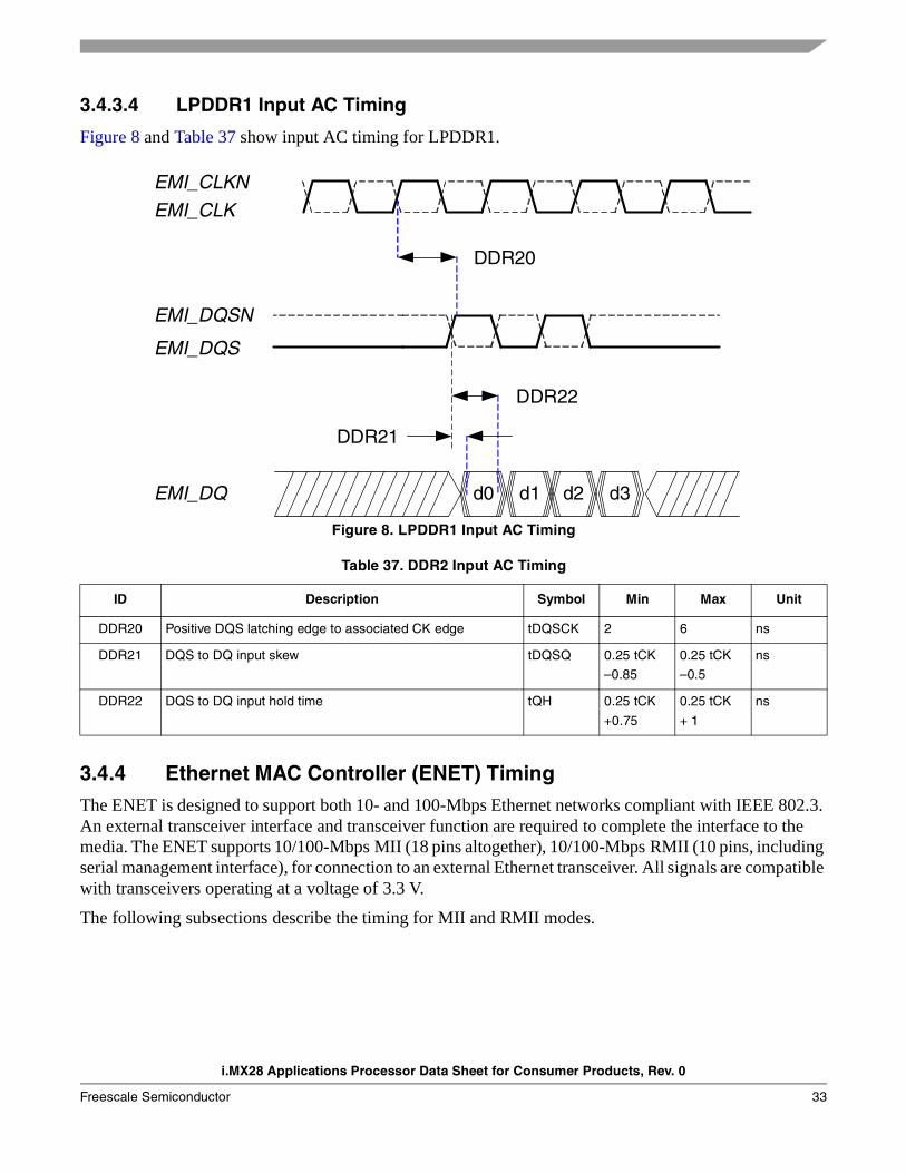
Figure 8 and Table 37 show input AC timing for LPDDR1.
Figure 8. LPDDR1 Input AC Timing
3.4.4 Ethernet MAC Controller (ENET) TimingThe ENET is designed to support both 10- and 100-Mbps Ethernet networks compliant with IEEE 802.3. An external transceiver interface and transceiver function are required to complete the interface to the media. The ENET supports 10/100-Mbps MII (18 pins altogether), 10/100-Mbps RMII (10 pins, including serial management interface), for connection to an external Ethernet transceiver. All signals are compatible with transceivers operating at a voltage of 3.3 V.
The following subsections describe the timing for MII and RMII modes.
Table 37. DDR2 Input AC Timing
ID Description Symbol Min Max Unit
DDR20 Positive DQS latching edge to associated CK edge tDQSCK 2 6 ns
DDR21 DQS to DQ input skew tDQSQ 0.25 tCK
–0.85
0.25 tCK
–0.5
ns
DDR22 DQS to DQ input hold time tQH 0.25 tCK
+0.75
0.25 tCK
+ 1
ns
EMI_CLK
EMI_CLKN
EMI_DQS
DDR21
DDR22
d0
DDR20
d1 d2 d3EMI_DQ
EMI_DQSN
i.MX28 Applications Processor Data Sheet for Consumer Products, Rev. 0
Freescale Semiconductor 33

3.4.4.1 ENET MII Mode Timing
This subsection describes MII receive, transmit, asynchronous inputs, and serial management signal timings.
3.4.4.1.1 MII Receive Signal Timing (ENET0_RXD[3:0], ENET0_RX_DV, ENET0_RX_ER, and ENET0_RX_CLK)
The receiver functions correctly up to an ENET0_RX_CLK maximum frequency of 25 MHz + 1%. There is no minimum frequency requirement. Additionally, the processor clock frequency must exceed twice the ENET0_RX_CLK frequency.
Figure 9 shows MII receive signal timings. Table 38 describes the timing parameters (M1–M4) shown in the figure.
Figure 9. MII Receive Signal Timing Diagram
1 ENET0_RX_DV, ENET0_RX_CLK, and ENET0_RXD0 have the same timing in 10 Mbps 7-wire interface mode.
3.4.4.1.2 MII Transmit Signal Timing (ENET0_TXD[3:0], ENET0_TX_EN, ENET0_TX_ER, and ENET0_TX_CLK)
The transmitter functions correctly up to an ENET0_TX_CLK maximum frequency of 25 MHz + 1%. There is no minimum frequency requirement. Additionally, the processor clock frequency must exceed twice the ENET0_TX_CLK frequency.
Table 38. MII Receive Signal Timing
ID Characteristic1 Min. Max. Unit
M1 ENET0_RXD[3:0], ENET0_RX_DV, ENET0_RX_ER to ENET0_RX_CLK setup
5 — ns
M2 ENET0_RX_CLK to ENET0_RXD[3:0], ENET0_RX_DV, ENET0_RX_ER hold
5 — ns
M3 ENET0_RX_CLK pulse width high 35% 65% ENET0_RX_CLK period
M4 ENET0_RX_CLK pulse width low 35% 65% ENET0_RX_CLK period
ENET0_RX_CLK (input)
ENET0_RXD[3:0] (inputs) ENET0_RX_DV ENET0_RX_ER
M3
M4
M1 M2
i.MX28 Applications Processor Data Sheet for Consumer Products, Rev. 0
34 Freescale Semiconductor
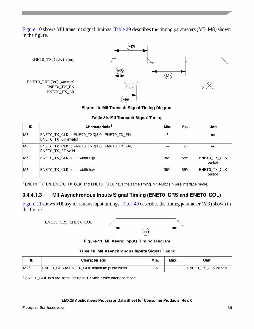
Figure 10 shows MII transmit signal timings. Table 39 describes the timing parameters (M5–M8) shown in the figure.
Figure 10. MII Transmit Signal Timing Diagram
1 ENET0_TX_EN, ENET0_TX_CLK, and ENET0_TXD0 have the same timing in 10-Mbps 7-wire interface mode.
3.4.4.1.3 MII Asynchronous Inputs Signal Timing (ENET0_CRS and ENET0_COL)
Figure 11 shows MII asynchronous input timings. Table 40 describes the timing parameter (M9) shown in the figure.
Figure 11. MII Async Inputs Timing Diagram
1 ENET0_COL has the same timing in 10-Mbit 7-wire interface mode.
Table 39. MII Transmit Signal Timing
ID Characteristic1 Min. Max. Unit
M5 ENET0_TX_CLK to ENET0_TXD[3:0], ENET0_TX_EN, ENET0_TX_ER invalid
5 — ns
M6 ENET0_TX_CLK to ENET0_TXD[3:0], ENET0_TX_EN, ENET0_TX_ER valid
— 20 ns
M7 ENET0_TX_CLK pulse width high 35% 65% ENET0_TX_CLK period
M8 ENET0_TX_CLK pulse width low 35% 65% ENET0_TX_CLK period
Table 40. MII Asynchronous Inputs Signal Timing
ID Characteristic Min. Max. Unit
M91 ENET0_CRS to ENET0_COL minimum pulse width 1.5 — ENET0_TX_CLK period
ENET0_TX_CLK (input)
ENET0_TXD[3:0] (outputs) ENET0_TX_EN ENET0_TX_ER
M7
M8M5
M6
ENET0_CRS, ENET0_COL
M9
i.MX28 Applications Processor Data Sheet for Consumer Products, Rev. 0
Freescale Semiconductor 35
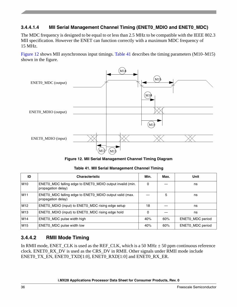
3.4.4.1.4 MII Serial Management Channel Timing (ENET0_MDIO and ENET0_MDC)
The MDC frequency is designed to be equal to or less than 2.5 MHz to be compatible with the IEEE 802.3 MII specification. However the ENET can function correctly with a maximum MDC frequency of 15 MHz.
Figure 12 shows MII asynchronous input timings. Table 41 describes the timing parameters (M10–M15) shown in the figure.
Figure 12. MII Serial Management Channel Timing Diagram
3.4.4.2 RMII Mode Timing
In RMII mode, ENET_CLK is used as the REF_CLK, which is a 50 MHz ± 50 ppm continuous reference clock. ENET0_RX_DV is used as the CRS_DV in RMII. Other signals under RMII mode include ENET0_TX_EN, ENET0_TXD[1:0], ENET0_RXD[1:0] and ENET0_RX_ER.
Table 41. MII Serial Management Channel Timing
ID Characteristic Min. Max. Unit
M10 ENET0_MDC falling edge to ENET0_MDIO output invalid (min. propagation delay)
0 — ns
M11 ENET0_MDC falling edge to ENET0_MDIO output valid (max. propagation delay)
— 5 ns
M12 ENET0_MDIO (input) to ENET0_MDC rising edge setup 18 — ns
M13 ENET0_MDIO (input) to ENET0_MDC rising edge hold 0 — ns
M14 ENET0_MDC pulse width high 40% 60% ENET0_MDC period
M15 ENET0_MDC pulse width low 40% 60% ENET0_MDC period
ENET0_MDC (output)
ENET0_MDIO (output)
M14
M15
M10
M11
M12 M13
ENET0_MDIO (input)
i.MX28 Applications Processor Data Sheet for Consumer Products, Rev. 0
36 Freescale Semiconductor
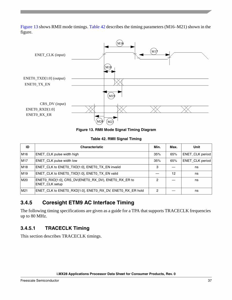
Figure 13 shows RMII mode timings. Table 42 describes the timing parameters (M16–M21) shown in the figure.
Figure 13. RMII Mode Signal Timing Diagram
3.4.5 Coresight ETM9 AC Interface TimingThe following timing specifications are given as a guide for a TPA that supports TRACECLK frequencies up to 80 MHz.
3.4.5.1 TRACECLK Timing
This section describes TRACECLK timings.
Table 42. RMII Signal Timing
ID Characteristic Min. Max. Unit
M16 ENET_CLK pulse width high 35% 65% ENET_CLK period
M17 ENET_CLK pulse width low 35% 65% ENET_CLK period
M18 ENET_CLK to ENET0_TXD[1:0], ENET0_TX_EN invalid 3 — ns
M19 ENET_CLK to ENET0_TXD[1:0], ENET0_TX_EN valid — 12 ns
M20 ENET0_RXD[1:0], CRS_DV(ENET0_RX_DV), ENET0_RX_ER to ENET_CLK setup
2 — ns
M21 ENET_CLK to ENET0_RXD[1:0], ENET0_RX_DV, ENET0_RX_ER hold 2 — ns
ENET_CLK (input)
ENET0_TX_EN
M16
M17
M18
M19
M20 M21
ENET0_RXD[1:0]
ENET0_TXD[1:0] (output)
ENET0_RX_ER
CRS_DV (input)
i.MX28 Applications Processor Data Sheet for Consumer Products, Rev. 0
Freescale Semiconductor 37
Figure 14 shows TRACECLK signal timings. Table 43 describes the timing parameters shown in the figure.
Figure 14. TRACECLK Signal Timing Diagram
3.4.5.2 Trace Data Signal Timing
Figure 15 shows the setup and hold requirements of the trace data pins with respect to TRACECLK. Table 44 describes the timing parameters shown in the figure.
Figure 15. MII Transmit Signal Timing Diagram
Table 43. MII Receive Signal Timing
ID Characteristic1 Min. Max. Unit
Tr Clock and data raise time 3 — ns
Tf Clock and data fall time 3 — ns
Twh High pulse wide 2 — ns
Twl Low pulse wide 2 — ns
Tcyc Clock period 12.5 — ns
Table 44. MII Transmit Signal Timing
ID Characteristic1 Min. Max. Unit
Ts Data setup 2 — ns
Th Data hold 2 — ns
i.MX28 Applications Processor Data Sheet for Consumer Products, Rev. 0
38 Freescale Semiconductor

3.4.6 FlexCAN AC Timing
Table 45 and Table 46 show voltage requirements for the FlexCAN transceiver Tx and Rx pins.
Figure 16 through Figure 19 show the FlexCAN timing, including timing of the standby and shutdown signals.
Figure 16. FlexCAN Timing Diagram
Table 45. Tx Pin Characteristics
Parameter Symbol Min. Typ. Max. Units
High-level output voltage VOH 2 — Vcc1 + 0.3
1 Vcc = +3.3 V ± 5%
V
Low-level output voltage VOL — 0.8 — V
Table 46. Rx Pin Characteristics
Parameter Symbol Min. Typ. Max. Units
High-level input voltage VIH 0.8 × Vcc1
1 Vcc = +3.3 V ± 5%
— Vcc1 V
Low-level input voltage VIL — 0.4 — V
TXD
VDIFF
RXD
VCC/2
tONTXD tOFFTXD
tONRXD tOFFRXD
VCC/2 VCC/2
0.5V
0.9V
VCC/2
i.MX28 Applications Processor Data Sheet for Consumer Products, Rev. 0
Freescale Semiconductor 39
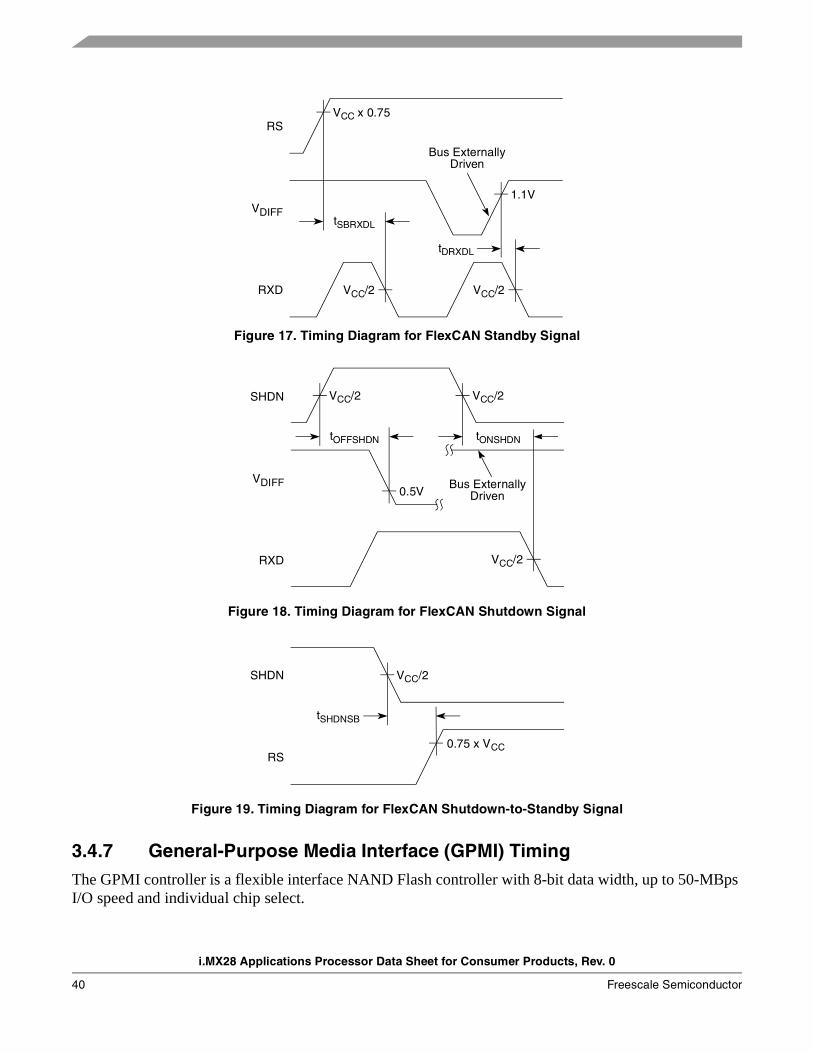
Figure 17. Timing Diagram for FlexCAN Standby Signal
Figure 18. Timing Diagram for FlexCAN Shutdown Signal
Figure 19. Timing Diagram for FlexCAN Shutdown-to-Standby Signal
3.4.7 General-Purpose Media Interface (GPMI) TimingThe GPMI controller is a flexible interface NAND Flash controller with 8-bit data width, up to 50-MBps I/O speed and individual chip select.
RS
VDIFF
RXD VCC/2 VCC/2
tSBRXDL
tDRXDL
1.1V
VCC x 0.75
Bus ExternallyDriven
SHDN
VDIFF
RXD VCC/2
VCC/2
Bus ExternallyDriven
tOFFSHDN tONSHDN
VCC/2
0.5V
SHDN
RS
VCC/2
0.75 x VCC
tSHDNSB
i.MX28 Applications Processor Data Sheet for Consumer Products, Rev. 0
40 Freescale Semiconductor

The GPMI controller supports normal timing mode with configurable timing parameters. AC timings are provided as multiplications of the clock cycle and fixed delay.
Figure 20 through Figure 23 depict the relative timing between GPMI signals at the module level for different operations under normal mode. Table 47 describes the timing parameters (NF1–NF17) that are shown in the figures.
Figure 20. Command Latch Cycle Timing Diagram
Figure 21. Address Latch Cycle Timing Diagram
CLE
CEn
WE
ALE
IO[7:0] Command
NF9NF8
NF1 NF2
NF5
NF3 NF4
NF6 NF7
CLE
CEn
WE
ALE
IO[7:0] Address
NF9NF8
NF1
NF5
NF3 NF4
NF6
NF11
NF10
NF7
i.MX28 Applications Processor Data Sheet for Consumer Products, Rev. 0
Freescale Semiconductor 41
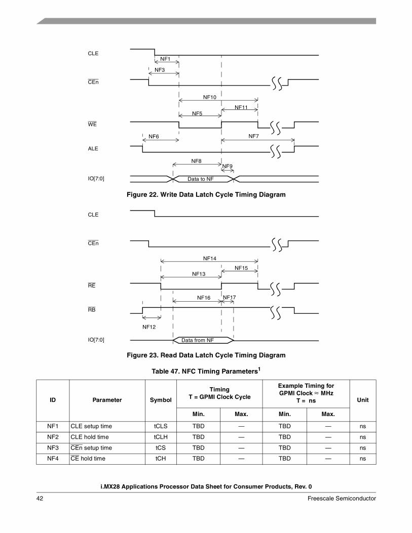
Figure 22. Write Data Latch Cycle Timing Diagram
Figure 23. Read Data Latch Cycle Timing Diagram
Table 47. NFC Timing Parameters1
ID Parameter Symbol
TimingT = GPMI Clock Cycle
Example Timing for GPMI Clock ≈ MHz
T = ns Unit
Min. Max. Min. Max.
NF1 CLE setup time tCLS TBD — TBD — ns
NF2 CLE hold time tCLH TBD — TBD — ns
NF3 CEn setup time tCS TBD — TBD — ns
NF4 CE hold time tCH TBD — TBD — ns
CLE
CEn
WE
ALE
IO[7:0] Data to NF
NF9NF8
NF1
NF5
NF3
NF6
NF11
NF10
NF7
CLE
CEn
RE
RB
IO[7:0] Data from NF
NF13NF15
NF14
NF17
NF12
NF16
i.MX28 Applications Processor Data Sheet for Consumer Products, Rev. 0
42 Freescale Semiconductor
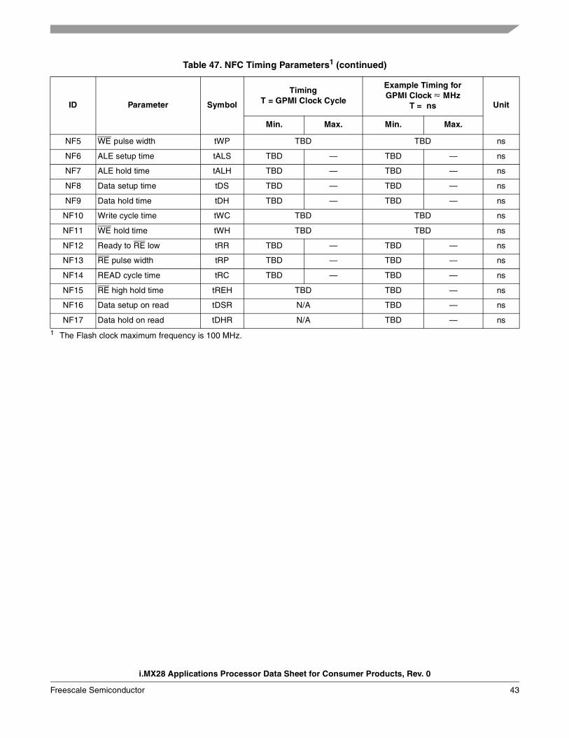
NF5 WE pulse width tWP TBD TBD ns
NF6 ALE setup time tALS TBD — TBD — ns
NF7 ALE hold time tALH TBD — TBD — ns
NF8 Data setup time tDS TBD — TBD — ns
NF9 Data hold time tDH TBD — TBD — ns
NF10 Write cycle time tWC TBD TBD ns
NF11 WE hold time tWH TBD TBD ns
NF12 Ready to RE low tRR TBD — TBD — ns
NF13 RE pulse width tRP TBD — TBD — ns
NF14 READ cycle time tRC TBD — TBD — ns
NF15 RE high hold time tREH TBD TBD — ns
NF16 Data setup on read tDSR N/A TBD — ns
NF17 Data hold on read tDHR N/A TBD — ns
1 The Flash clock maximum frequency is 100 MHz.
Table 47. NFC Timing Parameters1 (continued)
ID Parameter Symbol
TimingT = GPMI Clock Cycle
Example Timing for GPMI Clock ≈ MHz
T = ns Unit
Min. Max. Min. Max.
i.MX28 Applications Processor Data Sheet for Consumer Products, Rev. 0
Freescale Semiconductor 43
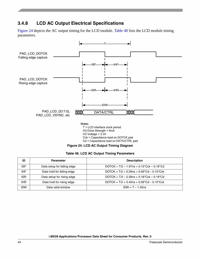
3.4.8 LCD AC Output Electrical Specifications
Figure 24 depicts the AC output timing for the LCD module. Table 48 lists the LCD module timing parameters.
Figure 24. LCD AC Output Timing Diagram
Table 48. LCD AC Output Timing Parameters
ID Parameter Description
tSF Data setup for falling edge DOTCK = T/2 – 1.97ns + 0.15*Cck – 0.19*Cd
tHF Data hold for falling edge DOTCK = T/2 + 0.29ns + 0.09*Cd – 0.10*Cck
tSR Data setup for rising edge DOTCK = T/2 – 2.09ns + 0.18*Cck – 0.19*Cd
tHR Data hold for rising edge DOTCK = T/2 + 0.40ns + 0.09*Cd – 0.10*Cck
tDW Data valid window tDW = T – 1.45ns
PAD_LCD_DOTCKFalling edge capture
Notes: T = LCD interface clock period I/O Drive Strength = 4mA I/O Voltage = 3.3V Cck = Capacitance load on DOTCK pad Cd = Capacitance load on DATA/CTRL pad
PAD_LCD_D[17:0], PAD_LCD_VSYNC, etc
DATA/CTRL
tDW
tSF tHF
PAD_LCD_DOTCKRising edge capture
tSR tHR
T
i.MX28 Applications Processor Data Sheet for Consumer Products, Rev. 0
44 Freescale Semiconductor
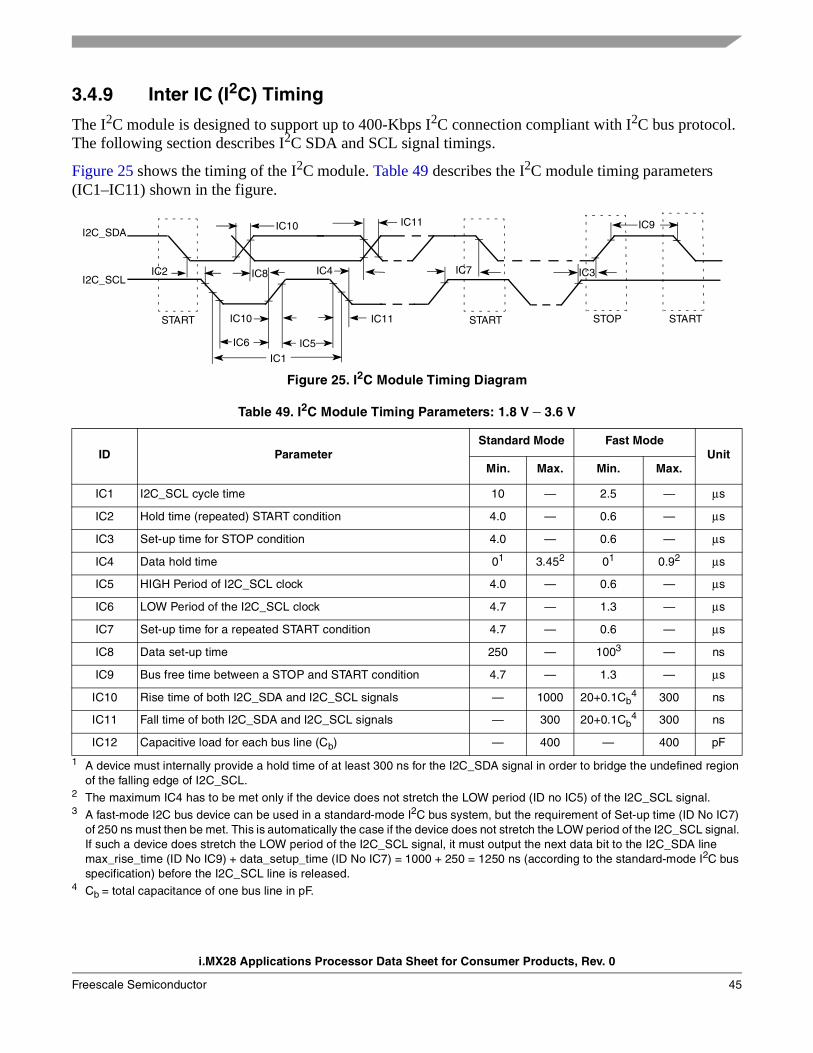
3.4.9 Inter IC (I2C) Timing
The I2C module is designed to support up to 400-Kbps I2C connection compliant with I2C bus protocol. The following section describes I2C SDA and SCL signal timings.
Figure 25 shows the timing of the I2C module. Table 49 describes the I2C module timing parameters (IC1–IC11) shown in the figure.
Figure 25. I2C Module Timing Diagram
Table 49. I2C Module Timing Parameters: 1.8 V – 3.6 V
ID ParameterStandard Mode Fast Mode
UnitMin. Max. Min. Max.
IC1 I2C_SCL cycle time 10 — 2.5 — μs
IC2 Hold time (repeated) START condition 4.0 — 0.6 — μs
IC3 Set-up time for STOP condition 4.0 — 0.6 — μs
IC4 Data hold time 01
1 A device must internally provide a hold time of at least 300 ns for the I2C_SDA signal in order to bridge the undefined region of the falling edge of I2C_SCL.
3.452
2 The maximum IC4 has to be met only if the device does not stretch the LOW period (ID no IC5) of the I2C_SCL signal.
01 0.92 μs
IC5 HIGH Period of I2C_SCL clock 4.0 — 0.6 — μs
IC6 LOW Period of the I2C_SCL clock 4.7 — 1.3 — μs
IC7 Set-up time for a repeated START condition 4.7 — 0.6 — μs
IC8 Data set-up time 250 — 1003
3 A fast-mode I2C bus device can be used in a standard-mode I2C bus system, but the requirement of Set-up time (ID No IC7) of 250 ns must then be met. This is automatically the case if the device does not stretch the LOW period of the I2C_SCL signal. If such a device does stretch the LOW period of the I2C_SCL signal, it must output the next data bit to the I2C_SDA line max_rise_time (ID No IC9) + data_setup_time (ID No IC7) = 1000 + 250 = 1250 ns (according to the standard-mode I2C bus specification) before the I2C_SCL line is released.
— ns
IC9 Bus free time between a STOP and START condition 4.7 — 1.3 — μs
IC10 Rise time of both I2C_SDA and I2C_SCL signals — 1000 20+0.1Cb4
4 Cb = total capacitance of one bus line in pF.
300 ns
IC11 Fall time of both I2C_SDA and I2C_SCL signals — 300 20+0.1Cb4 300 ns
IC12 Capacitive load for each bus line (Cb) — 400 — 400 pF
IC10 IC11 IC9
IC2 IC8 IC4 IC7 IC3
IC6
IC10
IC5
IC11 START STOP STARTSTART
I2C_SDA
I2C_SCL
IC1
i.MX28 Applications Processor Data Sheet for Consumer Products, Rev. 0
Freescale Semiconductor 45

3.4.10 JTAG Interface Timing
Figure 26 through Figure 29 show respectively the test clock input, boundary scan, test access port, and TRST timings for the SJC. Table 50 describes the SJC timing parameters (SJ1–SJ13) indicated in the figures.
Figure 26. Test Clock Input Timing Diagram
Figure 27. Boundary Scan (JTAG) Timing Diagram
TCK(Input) VM VMVIH
VIL
SJ1
SJ2 SJ2
SJ3SJ3
TCK(Input)
DataInputs
DataOutputs
DataOutputs
DataOutputs
VIHVIL
Input Data Valid
Output Data Valid
Output Data Valid
SJ4 SJ5
SJ6
SJ7
SJ6
i.MX28 Applications Processor Data Sheet for Consumer Products, Rev. 0
46 Freescale Semiconductor
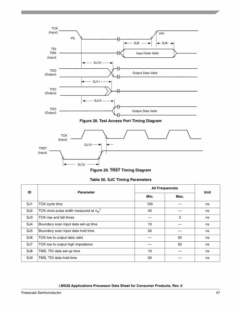
Figure 28. Test Access Port Timing Diagram
Figure 29. TRST Timing Diagram
Table 50. SJC Timing Parameters
ID ParameterAll Frequencies
Unit Min. Max.
SJ1 TCK cycle time 100 — ns
SJ2 TCK clock pulse width measured at VM1 40 — ns
SJ3 TCK rise and fall times — 3 ns
SJ4 Boundary scan input data set-up time 10 — ns
SJ5 Boundary scan input data hold time 50 — ns
SJ6 TCK low to output data valid — 50 ns
SJ7 TCK low to output high impedance — 50 ns
SJ8 TMS, TDI data set-up time 10 — ns
SJ9 TMS, TDI data hold time 50 — ns
TCK(Input)
TDI
(Input)
TDO(Output)
TDO(Output)
TDO(Output)
VIH
VIL
Input Data Valid
Output Data Valid
Output Data Valid
TMS
SJ8 SJ9
SJ10
SJ11
SJ10
TCK(Input)
TRST(Input)
SJ13
SJ12
i.MX28 Applications Processor Data Sheet for Consumer Products, Rev. 0
Freescale Semiconductor 47

3.4.11 Pulse Width Modulator (PWM) Timing
Figure 30 depicts the timing of the PWM, and Table 51 lists the PWM timing characteristics.
The PWM can be programmed to select one of two clock signals as its source frequency, xtal clock or hsadc clock. The selected clock signal is passed through a prescaler before being input to the counter. The output is available at the pulse width modulator output (PWMO) external pin.
PWM also supports MATT mode. In this mode, it can be programmed to select one of two clock signals as its source frequency, 24-MHz or 32-KHz crystal clock. For a 32-KHz source clock input, the PWM outputs the 32-KHz clock directly to PAD.
Figure 30. PWM Timing
SJ10 TCK low to TDO data valid — 44 ns
SJ11 TCK low to TDO high impedance — 44 ns
SJ12 TRST assert time 100 — ns
SJ13 TRST set-up time to TCK low 40 — ns
1 VM – mid point voltage
Table 51. PWM Output Timing Parameter: Xtal clock
Ref No. Parameter Minimum Maximum Unit
1 System CLK frequency1
1 CL of PWMO = 30 pF
0 24MHz MHz
2a Clock high time 21 — ns
2b Clock low time 21 — ns
3a Clock fall time — 0.3 ns
3b Clock rise time — 0.3 ns
4a Output delay time — 15.08 ns
4b Output setup time 15.77 — ns
Table 50. SJC Timing Parameters (continued)
ID ParameterAll Frequencies
Unit Min. Max.
4a
PWM Source Clock
2a1
PWM Output
2b
3a
3b
4b
i.MX28 Applications Processor Data Sheet for Consumer Products, Rev. 0
48 Freescale Semiconductor
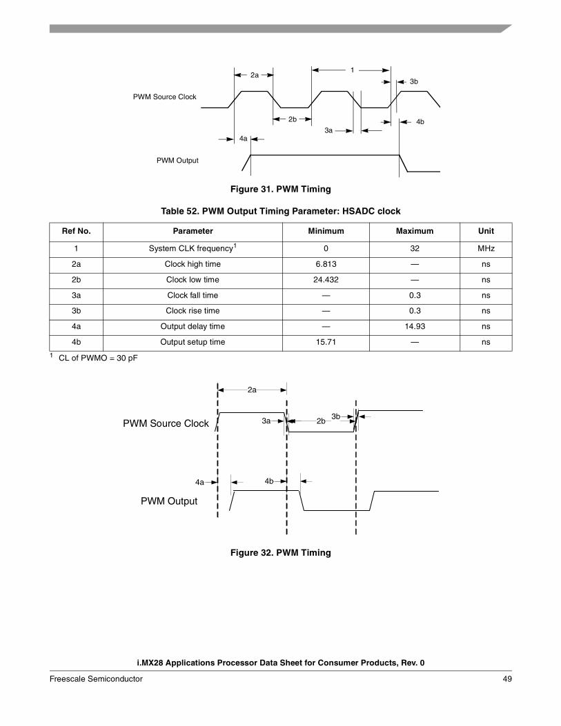
Figure 31. PWM Timing
Figure 32. PWM Timing
Table 52. PWM Output Timing Parameter: HSADC clock
Ref No. Parameter Minimum Maximum Unit
1 System CLK frequency1
1 CL of PWMO = 30 pF
0 32 MHz
2a Clock high time 6.813 — ns
2b Clock low time 24.432 — ns
3a Clock fall time — 0.3 ns
3b Clock rise time — 0.3 ns
4a Output delay time — 14.93 ns
4b Output setup time 15.71 — ns
4a
PWM Source Clock
2a1
PWM Output
2b
3a
3b
4b
PWM Source Clock
PWM Output
2a
4a
3a 2b3b
4b
i.MX28 Applications Processor Data Sheet for Consumer Products, Rev. 0
Freescale Semiconductor 49

3.4.12 Serial Audio Interface (SAIF) AC Timing
The following subsections describe SAIF timing in two cases:
• Transmitter
• Receiver
3.4.12.1 SAIF Transmitter Timing
Figure 33 shows the timing for SAIF transmitter with internal clock, and Table 54 describes the timing parameters (SS1–SS13).
Figure 33. SAIF Transmitter Timing Diagram
Table 53. PWM Output Timing Parameter: MATT Mode 24 MHz Crystal Clock
Ref No. Parameter Minimum Maximum Unit
1 System CLK frequency1
1 CL of PWMO = 30 pF
24 24 MHz
2a Clock high time 20.99 — ns
2b Clock low time 21.01 — ns
3a Clock fall time — 0.3 ns
3b Clock rise time — 0.3 ns
4a Output delay time — 15.23 ns
4b Output setup time 15.92 — ns
BITCLK
LRCLK
SS1
SDATA0-2
SS2 SS4
SS3SS5
SS6 SS7
SS8SS9
SS12SS13SS10
SS11
i.MX28 Applications Processor Data Sheet for Consumer Products, Rev. 0
50 Freescale Semiconductor
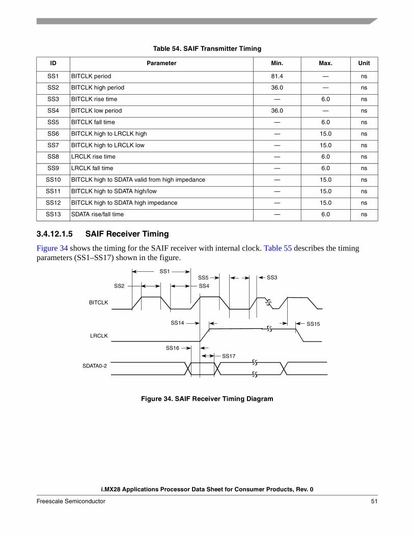
3.4.12.1.5 SAIF Receiver Timing
Figure 34 shows the timing for the SAIF receiver with internal clock. Table 55 describes the timing parameters (SS1–SS17) shown in the figure.
Figure 34. SAIF Receiver Timing Diagram
Table 54. SAIF Transmitter Timing
ID Parameter Min. Max. Unit
SS1 BITCLK period 81.4 — ns
SS2 BITCLK high period 36.0 — ns
SS3 BITCLK rise time — 6.0 ns
SS4 BITCLK low period 36.0 — ns
SS5 BITCLK fall time — 6.0 ns
SS6 BITCLK high to LRCLK high — 15.0 ns
SS7 BITCLK high to LRCLK low — 15.0 ns
SS8 LRCLK rise time — 6.0 ns
SS9 LRCLK fall time — 6.0 ns
SS10 BITCLK high to SDATA valid from high impedance — 15.0 ns
SS11 BITCLK high to SDATA high/low — 15.0 ns
SS12 BITCLK high to SDATA high impedance — 15.0 ns
SS13 SDATA rise/fall time — 6.0 ns
BITCLK
LRCLK
SDATA0-2
SS1
SS4SS2
SS16
SS17
SS14 SS15
SS3SS5
i.MX28 Applications Processor Data Sheet for Consumer Products, Rev. 0
Freescale Semiconductor 51
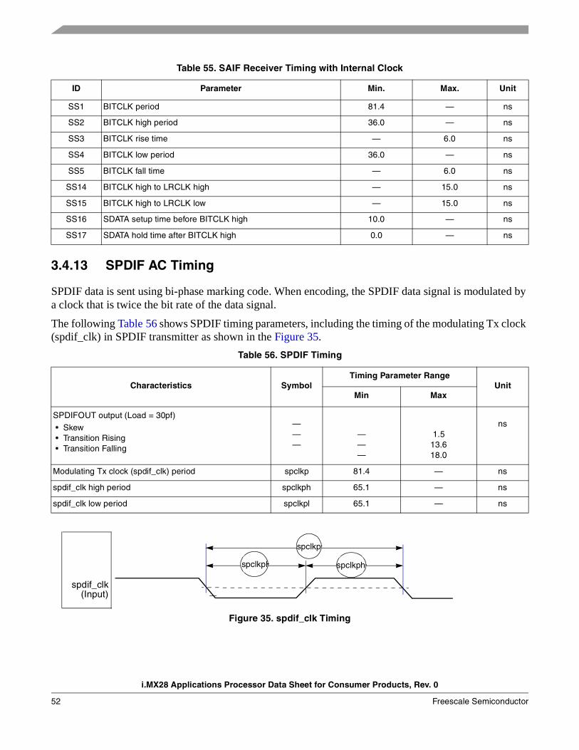
3.4.13 SPDIF AC Timing
SPDIF data is sent using bi-phase marking code. When encoding, the SPDIF data signal is modulated by a clock that is twice the bit rate of the data signal.
The following Table 56 shows SPDIF timing parameters, including the timing of the modulating Tx clock (spdif_clk) in SPDIF transmitter as shown in the Figure 35.
Figure 35. spdif_clk Timing
Table 55. SAIF Receiver Timing with Internal Clock
ID Parameter Min. Max. Unit
SS1 BITCLK period 81.4 — ns
SS2 BITCLK high period 36.0 — ns
SS3 BITCLK rise time — 6.0 ns
SS4 BITCLK low period 36.0 — ns
SS5 BITCLK fall time — 6.0 ns
SS14 BITCLK high to LRCLK high — 15.0 ns
SS15 BITCLK high to LRCLK low — 15.0 ns
SS16 SDATA setup time before BITCLK high 10.0 — ns
SS17 SDATA hold time after BITCLK high 0.0 — ns
Table 56. SPDIF Timing
Characteristics SymbolTiming Parameter Range
Unit Min Max
SPDIFOUT output (Load = 30pf)
• Skew • Transition Rising • Transition Falling
———
———
1.513.618.0
ns
Modulating Tx clock (spdif_clk) period spclkp 81.4 — ns
spdif_clk high period spclkph 65.1 — ns
spdif_clk low period spclkpl 65.1 — ns
spdif_clk(Input)
spclkp
spclkphspclkpl
i.MX28 Applications Processor Data Sheet for Consumer Products, Rev. 0
52 Freescale Semiconductor
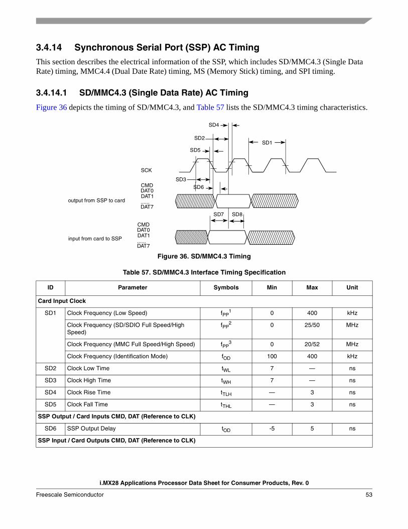
3.4.14 Synchronous Serial Port (SSP) AC TimingThis section describes the electrical information of the SSP, which includes SD/MMC4.3 (Single Data Rate) timing, MMC4.4 (Dual Date Rate) timing, MS (Memory Stick) timing, and SPI timing.
3.4.14.1 SD/MMC4.3 (Single Data Rate) AC Timing
Figure 36 depicts the timing of SD/MMC4.3, and Table 57 lists the SD/MMC4.3 timing characteristics.
Figure 36. SD/MMC4.3 Timing
Table 57. SD/MMC4.3 Interface Timing Specification
ID Parameter Symbols Min Max Unit
Card Input Clock
SD1 Clock Frequency (Low Speed) fPP1 0 400 kHz
Clock Frequency (SD/SDIO Full Speed/High Speed)
fPP2 0 25/50 MHz
Clock Frequency (MMC Full Speed/High Speed) fPP3 0 20/52 MHz
Clock Frequency (Identification Mode) fOD 100 400 kHz
SD2 Clock Low Time tWL 7 — ns
SD3 Clock High Time tWH 7 — ns
SD4 Clock Rise Time tTLH — 3 ns
SD5 Clock Fall Time tTHL — 3 ns
SSP Output / Card Inputs CMD, DAT (Reference to CLK)
SD6 SSP Output Delay tOD -5 5 ns
SSP Input / Card Outputs CMD, DAT (Reference to CLK)
SD1
SD3
SD5
SD4
SD7
CMD
output from SSP to cardDAT1......DAT7
DAT0
CMD
input from card to SSP DAT1......DAT7
DAT0
SCK
SD2
SD8
SD6
i.MX28 Applications Processor Data Sheet for Consumer Products, Rev. 0
Freescale Semiconductor 53

3.4.14.2 MMC4.4 (Dual Data Rate) AC Timing
Figure 37 depicts the timing of MMC4.4, and Table 58 lists the MMC4.4 timing characteristics. Be aware that only DATA0–DATA7 are sampled on both edges of the clock (not applicable to CMD).
Figure 37. MMC4.4 Timing
SD7 SSP Input Setup Time tISU 2.5 — ns
SD8 SSP Input Hold Time tIH4 2.5 — ns
1 In low speed mode, the card clock must be lower than 400 kHz, and the voltage ranges from 2.7 to 3.6 V.2 In normal speed mode for the SD/SDIO card, clock frequency can be any value between 0 ~ 25 MHz. In high speed mode,
clock frequency can be any value between 0 ~ 50 MHz.3 In normal speed mode for MMC card, clock frequency can be any value between 0 ~ 20 MHz. In high speed mode, clock
frequency can be any value between 0 ~ 52MHz.4 To satisfy hold timing, the delay difference between clock input and cmd/data input must not exceed 2ns.
Table 58. MMC4.4 Interface Timing Specification
ID Parameter Symbols Min Max Unit
Card Input Clock
SD1 Clock Frequency (MMC Full Speed/High Speed) fPP 0 52 MHz
SSP Output / Card Inputs CMD, DAT (Reference to CLK)
SD2 SSP Output Delay tOD –5 5 ns
SSP Input / Card Outputs CMD, DAT (Reference to CLK)
SD3 SSP Input Setup Time tISU 2.5 — ns
SD4 SSP Input Hold Time tIH 2.5 — ns
Table 57. SD/MMC4.3 Interface Timing Specification (continued)
ID Parameter Symbols Min Max Unit
SD1
SD2
SD3
output from SSP to cardDAT1......DAT7
DAT0
input from card to SSP DAT1......DAT7
DAT0
SCK
SD4
SD2
......
......
i.MX28 Applications Processor Data Sheet for Consumer Products, Rev. 0
54 Freescale Semiconductor
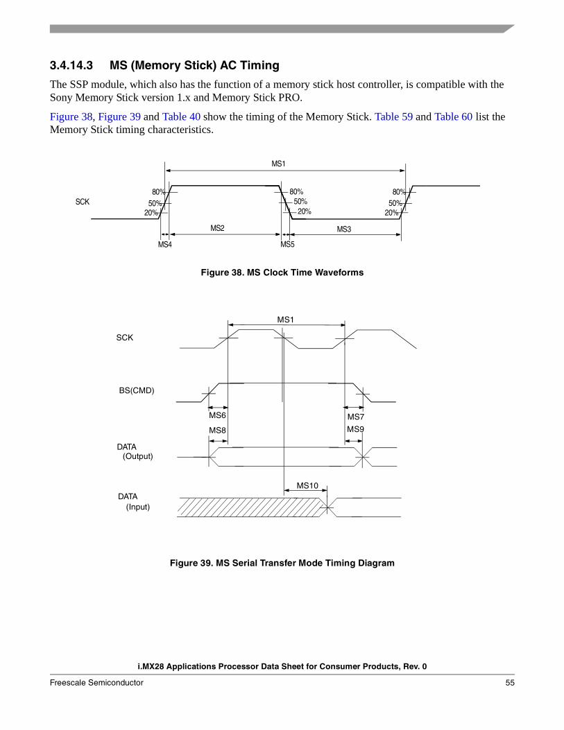
3.4.14.3 MS (Memory Stick) AC Timing
The SSP module, which also has the function of a memory stick host controller, is compatible with the Sony Memory Stick version 1.x and Memory Stick PRO.
Figure 38, Figure 39 and Table 40 show the timing of the Memory Stick. Table 59 and Table 60 list the Memory Stick timing characteristics.
Figure 38. MS Clock Time Waveforms
Figure 39. MS Serial Transfer Mode Timing Diagram
20%
80% 80%
20%SCK 50% 50%
20%
80%50%
MS4
MS2
MS5
MS3
MS1
SCK
BS(CMD)
DATA(Output)
DATA(Input)
MS1
MS6 MS7
MS8 MS9
MS10
i.MX28 Applications Processor Data Sheet for Consumer Products, Rev. 0
Freescale Semiconductor 55
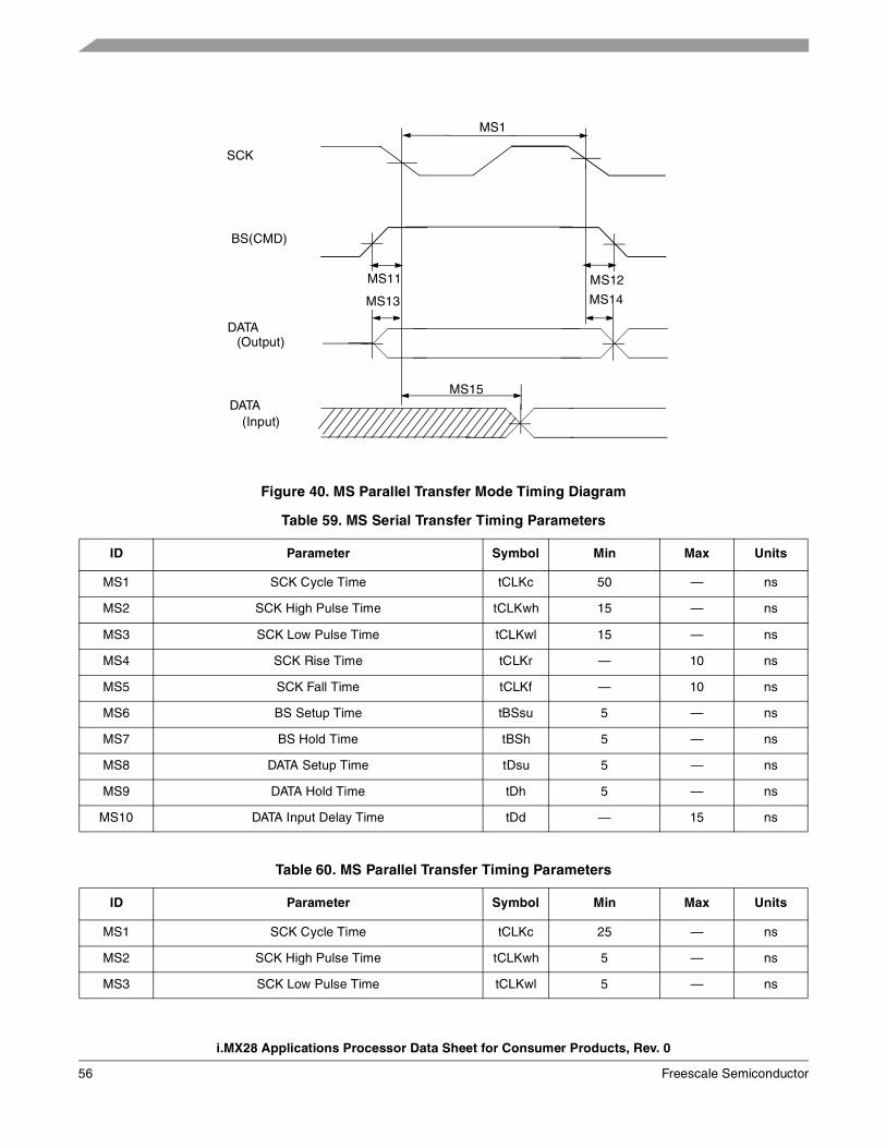
Figure 40. MS Parallel Transfer Mode Timing Diagram
Table 59. MS Serial Transfer Timing Parameters
ID Parameter Symbol Min Max Units
MS1 SCK Cycle Time tCLKc 50 — ns
MS2 SCK High Pulse Time tCLKwh 15 — ns
MS3 SCK Low Pulse Time tCLKwl 15 — ns
MS4 SCK Rise Time tCLKr — 10 ns
MS5 SCK Fall Time tCLKf — 10 ns
MS6 BS Setup Time tBSsu 5 — ns
MS7 BS Hold Time tBSh 5 — ns
MS8 DATA Setup Time tDsu 5 — ns
MS9 DATA Hold Time tDh 5 — ns
MS10 DATA Input Delay Time tDd — 15 ns
Table 60. MS Parallel Transfer Timing Parameters
ID Parameter Symbol Min Max Units
MS1 SCK Cycle Time tCLKc 25 — ns
MS2 SCK High Pulse Time tCLKwh 5 — ns
MS3 SCK Low Pulse Time tCLKwl 5 — ns
SCK
BS(CMD)
DATA(Output)
DATA(Input)
MS1
MS11 MS12
MS13 MS14
MS15
i.MX28 Applications Processor Data Sheet for Consumer Products, Rev. 0
56 Freescale Semiconductor

3.4.14.4 SPI AC Timing
Figure 41 depicts the master mode and slave mode timings of the SPI, and Table 61 lists the timing parameters.
Figure 41. SPI Interface Timing Diagram
MS4 SCK Rise Time tCLKr — 10 ns
MS5 SCK Fall Time tCLKf — 10 ns
MS11 BS Setup Time tBSsu 8 — ns
MS12 BS Hold Time tBSh 1 — ns
MS13 DATA Setup Time tDsu 8 — ns
MS14 DATA Hold Time tDh 1 — ns
MS15 DATA Input Delay Time tDd — 15 ns
Table 61. SPI Interface Timing Parameters
ID Parameter Symbol Min. Max. Units
CS1 SCK cycle time tclk 50 — ns
CS2 SCK high or low time tSW 25 — ns
CS3 SCK rise or fall tRISE/FALL — 7.6 ns
CS4 SSn pulse width tCSLH 25 — ns
CS5 SSn lead time (CS setup time) tSCS 25 — ns
CS6 SSn lag time (CS hold time) tHCS 25 — ns
CS7 MOSI setup time tSmosi 5 — ns
CS8 MOSI hold time tHmosi 5 — ns
CS9 MISO setup time tSmiso 5 — ns
CS10 MISO hold time tHmiso 5 — ns
Table 60. MS Parallel Transfer Timing Parameters (continued)
ID Parameter Symbol Min Max Units
CS7 CS8
CS2
CS2
CS4CS6
CS9 CS10
SCK
SSn
MISO
MOSI
CS1 CS3
CS3
CS5
i.MX28 Applications Processor Data Sheet for Consumer Products, Rev. 0
Freescale Semiconductor 57
3.4.15 UART (UARTAPP and DebugUART) AC TimingThis section describes the UART module AC timing which is applicable to both UARTAPP and DebugUART.
3.4.15.1 UART Transmit Timing
Figure 39 shows the UART transmit timing, showing only 8 data bits and 1 stop bit. Table 62 describes the timing parameter (UA1) shown in the figure.
Figure 42. UART Transmit Timing Diagram
3.4.15.2 UART Receive Timing
Figure 43 shows the UART receive timing, showing only 8 data bits and 1 stop bit. Table 63 describes the timing parameter (UA2) shown in the figure.
–
Figure 43. UART Receive Timing Diagram
Table 62. UART Transmit Timing Parameters
ID Parameter Symbol Min. Max. Units
UA1 Transmit Bit Time tTbit 1/Fbaud_rate1 – Tref_clk
2
1 Fbaud_rate: Baud rate frequency. The maximum baud rate the UARTAPP can support is 3.25 Mbps. The maximum baud rate of DebugUART is 115.2 kbps.
2 Tref_clk: The period of UART reference clock ref_clk (which is APBX clock = 24 MHz).
1/Fbaud_rate + Tref_clk —
Bit 1 Bit 2Bit 0 Bit 4 Bit 5 Bit 6 Bit 7TXD(output)
Bit 3StartBit STOP
BIT
NextStartBit
PossibleParity
Bit
Par Bit
UA1
UA1 UA1
UA1
Bit 1 Bit 2Bit 0 Bit 4 Bit 5 Bit 6 Bit 7RXD
(input) Bit 3StartBit STOP
BIT
NextStartBit
PossibleParity
Bit
Par Bit
UA2 UA2
UA2 UA2
i.MX28 Applications Processor Data Sheet for Consumer Products, Rev. 0
58 Freescale Semiconductor
4 Package Information and Contact Assignment
4.1 289-Ball MAPBGA—Case 14 x 14 mm, 0.8 mm PitchThe following notes apply to Figure 44:
• All dimensions are in millimeters.
• Dimensioning and tolerancing per ASME Y14.5M-1994.
• Maximum solder bump diameter measured parallel to datum A.
• Datum A, the seating plane, is determined by the spherical crowns of the solder bumps.
• Parallelism measurement shall exclude any effect of mark on top surface of package.
Table 63. UART Receive Timing Parameters
ID Parameter Symbol Min. Max. Units
UA2 Receive bit time1
1 The UART receiver can tolerate 1/(16 × Fbaud_rate) tolerance in each bit. But accumulation tolerance in one frame must not exceed 3/(16 × Fbaud_rate).
tRbit 1/Fbaud_rate2 – 1/(16
× Fbaud_rate)
2 Fbaud_rate: Baud rate frequency. The maximum baud rate the UARTAPP can support is 3.25 Mbps. The maximum baud rate of DebugUART is 115 kbps.
1/Fbaud_rate + 1/(16 × Fbaud_rate)
—
i.MX28 Applications Processor Data Sheet for Consumer Products, Rev. 0
Freescale Semiconductor 59
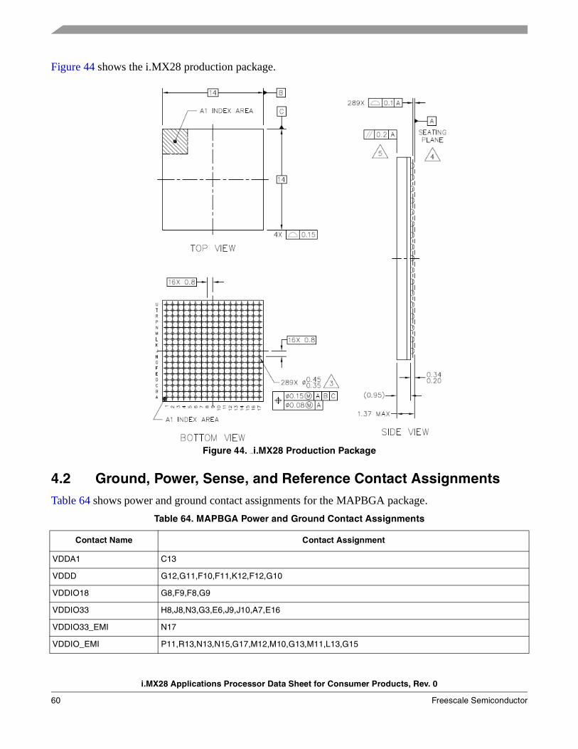
Figure 44 shows the i.MX28 production package.
Figure 44. zzxzi.MX28 Production Package
4.2 Ground, Power, Sense, and Reference Contact AssignmentsTable 64 shows power and ground contact assignments for the MAPBGA package.
Table 64. MAPBGA Power and Ground Contact Assignments
Contact Name Contact Assignment
VDDA1 C13
VDDD G12,G11,F10,F11,K12,F12,G10
VDDIO18 G8,F9,F8,G9
VDDIO33 H8,J8,N3,G3,E6,J9,J10,A7,E16
VDDIO33_EMI N17
VDDIO_EMI P11,R13,N13,N15,G17,M12,M10,G13,M11,L13,G15
i.MX28 Applications Processor Data Sheet for Consumer Products, Rev. 0
60 Freescale Semiconductor

4.3 Signal Contact AssignmentsTable 65 lists the i.MX287 MAPBGA package signal contact assignments.
VDDIO_EMIQ K15,J13,R15
VDDXTAL C12
VSS E15,L11,A1,K10,K11,J11,M14,H11,U1,H9,H12,H3,K9,C16,L10,H16,J12,H10,B7,E5,J15,A9,N4
VSSA1 B13
VSSA2 B11
VSSIO_EMI F16,R10,H14,M16,F14,L12,P16,U17,T14,P14,R12
Table 65. MAPBGA Contact Assignments
Signal NameContact
Assignment Signal NameContact
Assignment Signal NameContact
Assignment
AUART0_CTS J6 EMI_DQS1N J16 LCD_D17 R3
AUART0_RTS J7 EMI_ODT0 R17 LCD_D18 U4
AUART0_RX G5 EMI_ODT1 T17 LCD_D19 T4
AUART0_TX H5 EMI_RASN R16 LCD_D20 R4
AUART1_CTS K5 EMI_VREF0 R14 LCD_D21 U5
AUART1_RTS J5 EMI_VREF1 K13 LCD_D22 T5
AUART1_RX L4 EMI_WEN T15 LCD_D23 R5
AUART1_TX K4 ENET0_COL J4 LCD_DOTCLK N1
AUART2_CTS H6 ENET0_CRS J3 LCD_ENABLE N5
AUART2_RTS H7 ENET0_MDC G4 LCD_HSYNC M1
AUART2_RX F6 ENET0_MDIO H4 LCD_RD_E P4
AUART2_TX F5 ENET0_RXD0 H1 LCD_RESET M6
AUART3_CTS L6 ENET0_RXD1 H2 LCD_RS M4
AUART3_RTS K6 ENET0_RXD2 J1 LCD_VSYNC L1
AUART3_RX M5 ENET0_RXD3 J2 LCD_WR_RWN K1
AUART3_TX L5 ENET0_RX_CLK F3 LRADC0 C15
BATTERY A15 ENET0_RX_EN E4 LRADC1 C9
DCDC_BATT B15 ENET0_TXD0 F1 LRADC2 C8
DCDC_GND A17 ENET0_TXD1 F2 LRADC3 D9
DCDC_LN1 B17 ENET0_TXD2 G1 LRADC4 D13
DCDC_LP A16 ENET0_TXD3 G2 LRADC5 D15
Table 64. MAPBGA Power and Ground Contact Assignments (continued)
Contact Name Contact Assignment
i.MX28 Applications Processor Data Sheet for Consumer Products, Rev. 0
Freescale Semiconductor 61

DCDC_VDDA B16 ENET0_TX_CLK E3 LRADC6 C14
DCDC_VDDD D17 ENET0_TX_EN F4 PSWITCH A11
DCDC_VDDIO C17 ENET_CLK E2 PWM0 K7
DEBUG B9 GPMI_ALE P6 PWM1 L7
EMI_A00 U15 GPMI_CE0N N7 PWM2 K8
EMI_A01 U12 GPMI_CE1N N9 PWM3 E9
EMI_A02 U14 GPMI_CE2N M7 PWM4 E10
EMI_A03 T11 GPMI_CE3N M9 RESETN A14
EMI_A04 U10 GPMI_CLE P7 RTC_XTALI D11
EMI_A05 R11 GPMI_D00 U8 RTC_XTALO C11
EMI_A06 R9 GPMI_D01 T8 SAIF0_BITCLK F7
EMI_A07 N11 GPMI_D02 R8 SAIF0_LRCLK G6
EMI_A08 U9 GPMI_D03 U7 SAIF0_MCLK G7
EMI_A09 P10 GPMI_D04 T7 SAIF0_SDATA0 E7
EMI_A10 U13 GPMI_D05 R7 SAIF1_SDATA0 E8
EMI_A11 T10 GPMI_D06 U6 SPDIF D7
EMI_A12 U11 GPMI_D07 T6 SSP0_CMD A4
EMI_A13 T9 GPMI_RDN R6 SSP0_DATA0 B6
EMI_A14 N10 GPMI_RDY0 N6 SSP0_DATA1 C6
EMI_BA0 T16 GPMI_RDY1 N8 SSP0_DATA2 D6
EMI_BA1 T12 GPMI_RDY2 M8 SSP0_DATA3 A5
EMI_BA2 N12 GPMI_RDY3 L8 SSP0_DATA4 B5
EMI_CASN U16 GPMI_RESETN L9 SSP0_DATA5 C5
EMI_CE0N P12 GPMI_WRN P8 SSP0_DATA6 D5
EMI_CE1N P9 HSADC0 B14 SSP0_DATA7 B4
EMI_CKE T13 I2C0_SCL C7 SSP0_DETECT D10
EMI_CLK L17 I2C0_SDA D8 SSP0_SCK A6
EMI_CLKN L16 JTAG_RTCK E14 SSP1_CMD C1
EMI_D00 N16 JTAG_TCK E11 SSP1_DATA0 D1
EMI_D01 M13 JTAG_TDI E12 SSP1_DATA3 E1
EMI_D02 P15 JTAG_TDO E13 SSP1_SCK B1
EMI_D03 N14 JTAG_TMS D12 SSP2_MISO B3
Table 65. MAPBGA Contact Assignments (continued)
Signal NameContact
AssignmentSignal Name
Contact Assignment
Signal NameContact
Assignment
i.MX28 Applications Processor Data Sheet for Consumer Products, Rev. 0
62 Freescale Semiconductor

EMI_D04 P13 JTAG_TRST D14 SSP2_MOSI C3
EMI_D05 P17 LCD_CS P5 SSP2_SCK A3
EMI_D06 L14 LCD_D00 K2 SSP2_SS0 C4
EMI_D07 M17 LCD_D01 K3 SSP2_SS1 D3
EMI_D08 G16 LCD_D02 L2 SSP2_SS2 D4
EMI_D09 H15 LCD_D03 L3 SSP3_MISO B2
EMI_D10 G14 LCD_D04 M2 SSP3_MOSI C2
EMI_D11 J14 LCD_D05 M3 SSP3_SCK A2
EMI_D12 H13 LCD_D06 N2 SSP3_SS0 D2
EMI_D13 H17 LCD_D07 P1 TESTMODE C10
EMI_D14 F13 LCD_D08 P2 USB0DM A10
EMI_D15 F17 LCD_D09 P3 USB0DP B10
EMI_DDR_OPEN
K14 LCD_D10 R1 USB1DM B8
EMI_DDR_OPEN_FB
L15 LCD_D11 R2 USB1DP A8
EMI_DQM0 M15 LCD_D12 T1 VDD1P5 D16
EMI_DQM1 F15 LCD_D13 T2 VDD4P2 A13
EMI_DQS0 K17 LCD_D14 U2 VDD5V E17
EMI_DQS0N K16 LCD_D15 U3 XTALI A12
EMI_DQS1 J17 LCD_D16 T3 XTALO B12
Table 65. MAPBGA Contact Assignments (continued)
Signal NameContact
AssignmentSignal Name
Contact Assignment
Signal NameContact
Assignment
i.MX28 Applications Processor Data Sheet for Consumer Products, Rev. 0
Freescale Semiconductor 63
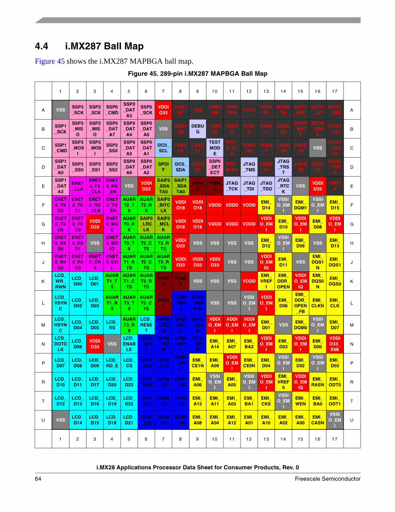
4.4 i.MX287 Ball MapFigure 45 shows the i.MX287 MAPBGA ball map.
Figure 45. 289-pin i.MX287 MAPBGA Ball Map
1 2 3 4 5 6 7 8 9 10 11 12 13 14 15 16 17
A VSSSSP3_SCK
SSP2_SCK
SSP0_CMD
SSP0_DAT
A3
SSP0_SCK
VDDIO33
USB1DP
VSSUSB0DM
PSWITCH
XTALIVDD4
P2RESE
TNBATTERY
DCDC_LP
DCDC_GND A
BSSP1_SCK
SSP3_MIS
O
SSP2_MIS
O
SSP0_DAT
A7
SSP0_DAT
A4
SSP0_DAT
A0VSS
USB1DM
DEBUG
USB0DP
VSSA2
XTALO
VSSA1
HSADC0
DCDC_BAT
T
DCDC_VDD
A
DCDC_LN1 B
CSSP1_CMD
SSP3_MOS
I
SSP2_MOS
I
SSP2_SS0
SSP0_DAT
A5
SSP0_DAT
A1
I2C0_SCL
LRADC2
LRADC1
TESTMOD
E
RTC_XTAL
O
VDDXTAL
VDDA1
LRADC6
LRADC0
VSSDCDC_VDD
IOC
DSSP1_DAT
A0
SSP3_SS0
SSP2_SS1
SSP2_SS2
SSP0_DAT
A6
SSP0_DAT
A2
SPDIF
I2C0_SDA
LRADC3
SSP0_DETECT
RTC_XTALI
JTAG_TMS
LRADC4
JTAG_TRS
T
LRADC5
VDD1P5
DCDC_VDD
DD
ESSP1_DAT
A3
ENET_CLK
ENET0_TX_CLK
ENET0_RX_EN
VSSVDDIO33
SAIF0_SDATA0
SAIF1_SDATA0
PWM3
PWM4
JTAG_TCK
JTAG_TDI
JTAG_TDO
JTAG_RTC
KVSS
VDDIO33
VDD5V E
FENET0_TXD0
ENET0_TX
D1
ENET0_RX_CLK
ENET0_TX_EN
AUART2_T
X
AUART2_R
X
SAIF0_BITC
LK
VDDIO18
VDDIO18
VDDD VDDD VDDDEMI_D14
VSSIO_EM
I
EMI_DQM1
VSSIO_EM
I
EMI_D15 F
GENET0_TXD2
ENET0_TX
D3
VDDIO33
ENET0_MD
C
AUART0_R
X
SAIF0_LRC
LK
SAIF0_MCL
K
VDDIO18
VDDIO18
VDDD VDDD VDDDVDDIO_EM
I
EMI_D10
VDDIO_EM
I
EMI_D08
VDDIO_EM
IG
HENET0_RX
D0
ENET0_RX
D1VSS
ENET0_MD
IO
AUART0_T
X
AUART2_C
TS
AUART2_R
TS
VDDIO33
VSS VSS VSS VSSEMI_D12
VSSIO_EM
I
EMI_D09
VSSEMI_D13 H
JENET0_RX
D2
ENET0_RX
D3
ENET0_CR
S
ENET0_CO
L
AUART1_R
TS
AUART0_C
TS
AUART0_R
TS
VDDIO33
VDDIO33
VDDIO33
VSS VSSVDDIO_EM
IQ
EMI_D11
VSSEMI_DQS1
N
EMI_DQS1 J
KLCD_WR_RWN
LCD_D00
LCD_D01
AUART1_T
X
AUART1_C
TS
AUART3_R
TS
PWM0
PWM2
VSS VSS VSS VDDDEMI_VREF
1
EMI_DDR_OPEN
VDDIO_EM
IQ
EMI_DQS0
N
EMI_DQS0 K
LLCD_VSYN
C
LCD_D02
LCD_D03
AUART1_R
X
AUART3_T
X
AUART3_C
TS
PWM1
GPMI_RDY
3
GPMI_RESETN
VSS VSSVSSIO_EM
I
VDDIO_EM
I
EMI_D06
EMI_DDR_OPEN_FB
EMI_CLKN
EMI_CLK L
MLCD_HSYN
C
LCD_D04
LCD_D05
LCD_RS
AUART3_R
X
LCD_RESE
T
GPMI_CE2
N
GPMI_RDY
2
GPMI_CE3
N
VDDIO_EM
I
VDDIO_EM
I
VDDIO_EM
I
EMI_D01
VSSEMI_DQM0
VSSIO_EM
I
EMI_D07 M
NLCD_DOTC
LK
LCD_D06
VDDIO33
VSSLCD_ENAB
LE
GPMI_RDY
0
GPMI_CE0
N
GPMI_RDY
1
GPMI_CE1
N
EMI_A14
EMI_A07
EMI_BA2
VDDIO_EM
I
EMI_D03
VDDIO_EM
I
EMI_D00
VDDIO33_EMI
N
PLCD_D07
LCD_D08
LCD_D09
LCD_RD_E
LCD_CS
GPMI_ALE
GPMI_CLE
GPMI_WR
N
EMI_CE1N
EMI_A09
VDDIO_EM
I
EMI_CE0N
EMI_D04
VSSIO_EM
I
EMI_D02
VSSIO_EM
I
EMI_D05 P
RLCD_D10
LCD_D11
LCD_D17
LCD_D20
LCD_D23
GPMI_RDN
GPMI_D05
GPMI_D02
EMI_A06
VSSIO_EM
I
EMI_A05
VSSIO_EM
I
VDDIO_EM
I
EMI_VREF
0
VDDIO_EM
IQ
EMI_RASN
EMI_ODT0 R
TLCD_D12
LCD_D13
LCD_D16
LCD_D19
LCD_D22
GPMI_D07
GPMI_D04
GPMI_D01
EMI_A13
EMI_A11
EMI_A03
EMI_BA1
EMI_CKE
VSSIO_EM
I
EMI_WEN
EMI_BA0
EMI_ODT1 T
U VSSLCD_D14
LCD_D15
LCD_D18
LCD_D21
GPMI_D06
GPMI_D03
GPMI_D00
EMI_A08
EMI_A04
EMI_A12
EMI_A01
EMI_A10
EMI_A02
EMI_A00
EMI_CASN
VSSIO_EM
IU
1 2 3 4 5 6 7 8 9 10 11 12 13 14 15 16 17
i.MX28 Applications Processor Data Sheet for Consumer Products, Rev. 0
64 Freescale Semiconductor
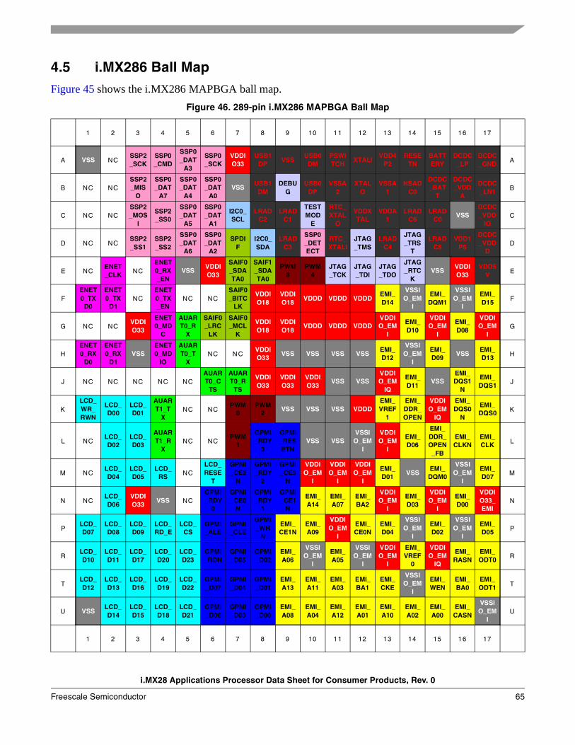
4.5 i.MX286 Ball MapFigure 45 shows the i.MX286 MAPBGA ball map.
Figure 46. 289-pin i.MX286 MAPBGA Ball Map
1 2 3 4 5 6 7 8 9 10 11 12 13 14 15 16 17
A VSS NCSSP2_SCK
SSP0_CMD
SSP0_DAT
A3
SSP0_SCK
VDDIO33
USB1DP
VSSUSB0DM
PSWITCH
XTALIVDD4
P2RESE
TNBATTERY
DCDC_LP
DCDC_GND A
B NC NCSSP2_MIS
O
SSP0_DAT
A7
SSP0_DAT
A4
SSP0_DAT
A0VSS
USB1DM
DEBUG
USB0DP
VSSA2
XTALO
VSSA1
HSADC0
DCDC_BAT
T
DCDC_VDD
A
DCDC_LN1 B
C NC NCSSP2_MOS
I
SSP2_SS0
SSP0_DAT
A5
SSP0_DAT
A1
I2C0_SCL
LRADC2
LRADC1
TESTMOD
E
RTC_XTAL
O
VDDXTAL
VDDA1
LRADC6
LRADC0
VSSDCDC_VDD
IOC
D NC NCSSP2_SS1
SSP2_SS2
SSP0_DAT
A6
SSP0_DAT
A2
SPDIF
I2C0_SDA
LRADC3
SSP0_DETECT
RTC_XTALI
JTAG_TMS
LRADC4
JTAG_TRS
T
LRADC5
VDD1P5
DCDC_VDD
DD
E NCENET_CLK NC
ENET0_RX_EN
VSSVDDIO33
SAIF0_SDATA0
SAIF1_SDATA0
PWM3
PWM4
JTAG_TCK
JTAG_TDI
JTAG_TDO
JTAG_RTC
KVSS
VDDIO33
VDD5V E
FENET0_TXD0
ENET0_TX
D1NC
ENET0_TX_EN
NC NCSAIF0_BITC
LK
VDDIO18
VDDIO18
VDDD VDDD VDDDEMI_D14
VSSIO_EM
I
EMI_DQM1
VSSIO_EM
I
EMI_D15 F
G NC NCVDDIO33
ENET0_MD
C
AUART0_R
X
SAIF0_LRC
LK
SAIF0_MCL
K
VDDIO18
VDDIO18
VDDD VDDD VDDDVDDIO_EM
I
EMI_D10
VDDIO_EM
I
EMI_D08
VDDIO_EM
IG
HENET0_RX
D0
ENET0_RX
D1VSS
ENET0_MD
IO
AUART0_T
XNC N C
VDDIO33
VSS VSS VSS VSSEMI_D12
VSSIO_EM
I
EMI_D09
VSSEMI_D13 H
J NC NC NC NC NCAUART0_C
TS
AUART0_R
TS
VDDIO33
VDDIO33
VDDIO33
VSS VSSVDDIO_EM
IQ
EMI_D11
VSSEMI_DQS1
N
EMI_DQS1 J
KLCD_WR_RWN
LCD_D00
LCD_D01
AUART1_T
XNC NC
PWM0
PWM2
VSS VSS VSS VDDDEMI_VREF
1
EMI_DDR_OPEN
VDDIO_EM
IQ
EMI_DQS0
N
EMI_DQS0 K
L NCLCD_D02
LCD_D03
AUART1_R
XNC NC
PWM1
GPMI_RDY
3
GPMI_RESETN
VSS VSSVSSIO_EM
I
VDDIO_EM
I
EMI_D06
EMI_DDR_OPEN_FB
EMI_CLKN
EMI_CLK L
M NCLCD_D04
LCD_D05
LCD_RS NC
LCD_RESE
T
GPMI_CE2
N
GPMI_RDY
2
GPMI_CE3
N
VDDIO_EM
I
VDDIO_EM
I
VDDIO_EM
I
EMI_D01
VSSEMI_DQM0
VSSIO_EM
I
EMI_D07 M
N NCLCD_D06
VDDIO33
VSS NCGPMI_RDY
0
GPMI_CE0
N
GPMI_RDY
1
GPMI_CE1
N
EMI_A14
EMI_A07
EMI_BA2
VDDIO_EM
I
EMI_D03
VDDIO_EM
I
EMI_D00
VDDIO33_EMI
N
PLCD_D07
LCD_D08
LCD_D09
LCD_RD_E
LCD_CS
GPMI_ALE
GPMI_CLE
GPMI_WR
N
EMI_CE1N
EMI_A09
VDDIO_EM
I
EMI_CE0N
EMI_D04
VSSIO_EM
I
EMI_D02
VSSIO_EM
I
EMI_D05 P
RLCD_D10
LCD_D11
LCD_D17
LCD_D20
LCD_D23
GPMI_RDN
GPMI_D05
GPMI_D02
EMI_A06
VSSIO_EM
I
EMI_A05
VSSIO_EM
I
VDDIO_EM
I
EMI_VREF
0
VDDIO_EM
IQ
EMI_RASN
EMI_ODT0 R
TLCD_D12
LCD_D13
LCD_D16
LCD_D19
LCD_D22
GPMI_D07
GPMI_D04
GPMI_D01
EMI_A13
EMI_A11
EMI_A03
EMI_BA1
EMI_CKE
VSSIO_EM
I
EMI_WEN
EMI_BA0
EMI_ODT1 T
U VSSLCD_D14
LCD_D15
LCD_D18
LCD_D21
GPMI_D06
GPMI_D03
GPMI_D00
EMI_A08
EMI_A04
EMI_A12
EMI_A01
EMI_A10
EMI_A02
EMI_A00
EMI_CASN
VSSIO_EM
IU
1 2 3 4 5 6 7 8 9 10 11 12 13 14 15 16 17
i.MX28 Applications Processor Data Sheet for Consumer Products, Rev. 0
Freescale Semiconductor 65
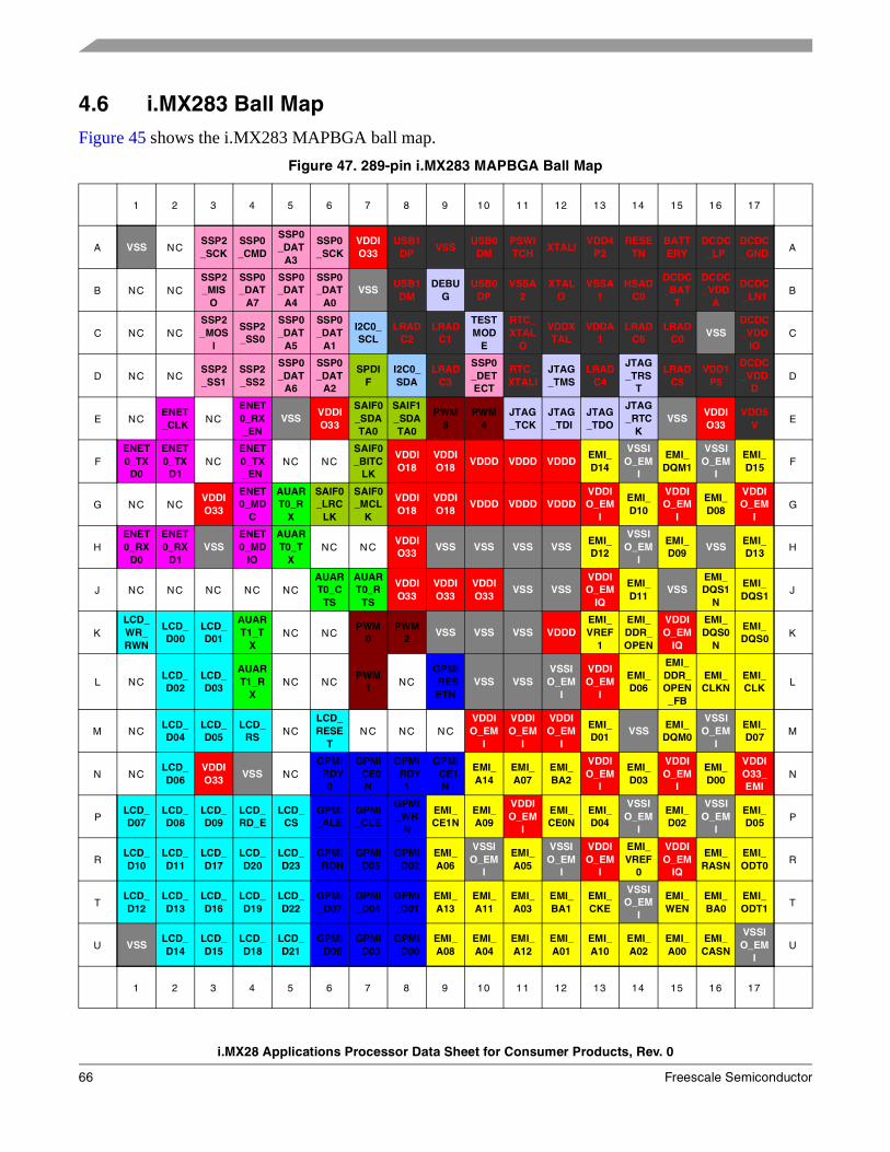
4.6 i.MX283 Ball MapFigure 45 shows the i.MX283 MAPBGA ball map.
Figure 47. 289-pin i.MX283 MAPBGA Ball Map
1 2 3 4 5 6 7 8 9 10 11 12 13 14 15 16 17
A VSS NCSSP2_SCK
SSP0_CMD
SSP0_DAT
A3
SSP0_SCK
VDDIO33
USB1DP
VSSUSB0DM
PSWITCH
XTALIVDD4
P2RESE
TNBATTERY
DCDC_LP
DCDC_GND A
B NC NCSSP2_MIS
O
SSP0_DAT
A7
SSP0_DAT
A4
SSP0_DAT
A0VSS
USB1DM
DEBUG
USB0DP
VSSA2
XTALO
VSSA1
HSADC0
DCDC_BAT
T
DCDC_VDD
A
DCDC_LN1 B
C NC NCSSP2_MOS
I
SSP2_SS0
SSP0_DAT
A5
SSP0_DAT
A1
I2C0_SCL
LRADC2
LRADC1
TESTMOD
E
RTC_XTAL
O
VDDXTAL
VDDA1
LRADC6
LRADC0
VSSDCDC_VDD
IOC
D NC NCSSP2_SS1
SSP2_SS2
SSP0_DAT
A6
SSP0_DAT
A2
SPDIF
I2C0_SDA
LRADC3
SSP0_DETECT
RTC_XTALI
JTAG_TMS
LRADC4
JTAG_TRS
T
LRADC5
VDD1P5
DCDC_VDD
DD
E NCENET_CLK NC
ENET0_RX_EN
VSSVDDIO33
SAIF0_SDATA0
SAIF1_SDATA0
PWM3
PWM4
JTAG_TCK
JTAG_TDI
JTAG_TDO
JTAG_RTC
KVSS
VDDIO33
VDD5V E
FENET0_TXD0
ENET0_TX
D1NC
ENET0_TX_EN
NC NCSAIF0_BITC
LK
VDDIO18
VDDIO18
VDDD VDDD VDDDEMI_D14
VSSIO_EM
I
EMI_DQM1
VSSIO_EM
I
EMI_D15 F
G NC NCVDDIO33
ENET0_MD
C
AUART0_R
X
SAIF0_LRC
LK
SAIF0_MCL
K
VDDIO18
VDDIO18
VDDD VDDD VDDDVDDIO_EM
I
EMI_D10
VDDIO_EM
I
EMI_D08
VDDIO_EM
IG
HENET0_RX
D0
ENET0_RX
D1VSS
ENET0_MD
IO
AUART0_T
XNC N C
VDDIO33
VSS VSS VSS VSSEMI_D12
VSSIO_EM
I
EMI_D09
VSSEMI_D13 H
J NC NC NC NC NCAUART0_C
TS
AUART0_R
TS
VDDIO33
VDDIO33
VDDIO33
VSS VSSVDDIO_EM
IQ
EMI_D11
VSSEMI_DQS1
N
EMI_DQS1 J
KLCD_WR_RWN
LCD_D00
LCD_D01
AUART1_T
XNC NC
PWM0
PWM2
VSS VSS VSS VDDDEMI_VREF
1
EMI_DDR_OPEN
VDDIO_EM
IQ
EMI_DQS0
N
EMI_DQS0 K
L NCLCD_D02
LCD_D03
AUART1_R
XNC NC
PWM1 NC
GPMI_RESETN
VSS VSSVSSIO_EM
I
VDDIO_EM
I
EMI_D06
EMI_DDR_OPEN_FB
EMI_CLKN
EMI_CLK L
M NCLCD_D04
LCD_D05
LCD_RS NC
LCD_RESE
TN C NC N C
VDDIO_EM
I
VDDIO_EM
I
VDDIO_EM
I
EMI_D01
VSSEMI_DQM0
VSSIO_EM
I
EMI_D07 M
N NCLCD_D06
VDDIO33
VSS NCGPMI_RDY
0
GPMI_CE0
N
GPMI_RDY
1
GPMI_CE1
N
EMI_A14
EMI_A07
EMI_BA2
VDDIO_EM
I
EMI_D03
VDDIO_EM
I
EMI_D00
VDDIO33_EMI
N
PLCD_D07
LCD_D08
LCD_D09
LCD_RD_E
LCD_CS
GPMI_ALE
GPMI_CLE
GPMI_WR
N
EMI_CE1N
EMI_A09
VDDIO_EM
I
EMI_CE0N
EMI_D04
VSSIO_EM
I
EMI_D02
VSSIO_EM
I
EMI_D05 P
RLCD_D10
LCD_D11
LCD_D17
LCD_D20
LCD_D23
GPMI_RDN
GPMI_D05
GPMI_D02
EMI_A06
VSSIO_EM
I
EMI_A05
VSSIO_EM
I
VDDIO_EM
I
EMI_VREF
0
VDDIO_EM
IQ
EMI_RASN
EMI_ODT0 R
TLCD_D12
LCD_D13
LCD_D16
LCD_D19
LCD_D22
GPMI_D07
GPMI_D04
GPMI_D01
EMI_A13
EMI_A11
EMI_A03
EMI_BA1
EMI_CKE
VSSIO_EM
I
EMI_WEN
EMI_BA0
EMI_ODT1 T
U VSSLCD_D14
LCD_D15
LCD_D18
LCD_D21
GPMI_D06
GPMI_D03
GPMI_D00
EMI_A08
EMI_A04
EMI_A12
EMI_A01
EMI_A10
EMI_A02
EMI_A00
EMI_CASN
VSSIO_EM
IU
1 2 3 4 5 6 7 8 9 10 11 12 13 14 15 16 17
i.MX28 Applications Processor Data Sheet for Consumer Products, Rev. 0
66 Freescale Semiconductor

5 Revision HistoryTable 66 summarizes revisions to this document.
Table 66. Revision History
Rev. Date Revision
0 09/2010 Initial release
i.MX28 Applications Processor Data Sheet for Consumer Products, Rev. 0
Freescale Semiconductor 67

i.MX28 Applications Processor Data Sheet for Consumer Products, Rev. 0
68 Freescale Semiconductor

i.MX28 Applications Processor Data Sheet for Consumer Products, Rev. 0
Freescale Semiconductor 69

How to Reach Us:
Document Number: IMX28CECRev. 009/2010
Home Page: www.freescale.com
Web Support: http://www.freescale.com/support
USA/Europe or Locations Not Listed: Freescale Semiconductor, Inc.Technical Information Center, EL5162100 East Elliot Road Tempe, Arizona 85284 1-800-521-6274 or+1-480-768-2130www.freescale.com/support
Europe, Middle East, and Africa:Freescale Halbleiter Deutschland GmbHTechnical Information CenterSchatzbogen 781829 Muenchen, Germany+44 1296 380 456 (English) +46 8 52200080 (English)+49 89 92103 559 (German)+33 1 69 35 48 48 (French) www.freescale.com/support
Japan: Freescale Semiconductor Japan Ltd. HeadquartersARCO Tower 15F1-8-1, Shimo-Meguro, Meguro-ku Tokyo 153-0064Japan 0120 191014 or+81 3 5437 [email protected]
Asia/Pacific: Freescale Semiconductor China Ltd. Exchange Building 23FNo. 118 Jianguo RoadChaoyang DistrictBeijing 100022China+86 10 5879 [email protected]
For Literature Requests Only:Freescale Semiconductor
Literature Distribution Center 1-800 441-2447 or+1-303-675-2140Fax: +1-303-675-2150LDCForFreescaleSemiconductor
@hibbertgroup.com
Information in this document is provided solely to enable system and software implementers to use Freescale Semiconductor products. There are no express or implied copyright licenses granted hereunder to design or fabricate any integrated circuits or integrated circuits based on the information in this document.
Freescale Semiconductor reserves the right to make changes without further notice to any products herein. Freescale Semiconductor makes no warranty, representation or guarantee regarding the suitability of its products for any particular purpose, nor does Freescale Semiconductor assume any liability arising out of the application or use of any product or circuit, and specifically disclaims any and all liability, including without limitation consequential or incidental damages. “Typical” parameters that may be provided in Freescale Semiconductor data sheets and/or specifications can and do vary in different applications and actual performance may vary over time. All operating parameters, including “Typicals”, must be validated for each customer application by customer’s technical experts. Freescale Semiconductor does not convey any license under its patent rights nor the rights of others. Freescale Semiconductor products are not designed, intended, or authorized for use as components in systems intended for surgical implant into the body, or other applications intended to support or sustain life, or for any other application in which the failure of the Freescale Semiconductor product could create a situation where personal injury or death may occur. Should Buyer purchase or use Freescale Semiconductor products for any such unintended or unauthorized application, Buyer shall indemnify and hold Freescale Semiconductor and its officers, employees, subsidiaries, affiliates, and distributors harmless against all claims, costs, damages, and expenses, and reasonable attorney fees arising out of, directly or indirectly, any claim of personal injury or death associated with such unintended or unauthorized use, even if such claim alleges that Freescale Semiconductor was negligent regarding the design or manufacture of the part.
RoHS-compliant and/or Pb-free versions of Freescale products have the functionality and electrical characteristics as their non-RoHS-compliant and/or non-Pb-free counterparts. For further information, see http://www.freescale.com or contact your Freescale sales representative.
For information on Freescale’s Environmental Products program, go to http://www.freescale.com/epp.
Freescale™ and the Freescale logo are trademarks of Freescale Semiconductor, Inc. All other product or service names are the property of their respective owners.ARM is the registered trademark of ARM Limited. ARM926EJ-S, CoreSight, and ETM9 are trademarks of ARM Limited. IEEE 1588 and IEEE 1149 are trademarks and IEEE 802.3 is a registered trademark of the Institute of Electrical and Electronics Engineers, Inc. (IEEE). This product is not endorsed or approved by the IEEE.
© Freescale Semiconductor, Inc., 2010. All rights reserved.