design and analysis of an ultrahigh-speed glitch-free fully differential charge pump with minimum...
TRANSCRIPT

IEEE TRANSACTIONS ON CIRCUITS AND SYSTEMS—II: EXPRESS BRIEFS, VOL. 53, NO. 9, SEPTEMBER 2006 843
Design and Analysis of an Ultrahigh-SpeedGlitch-Free Fully Differential Charge Pump
With Minimum Output Current Variationand Accurate Matching
Shanfeng Cheng, Student Member, IEEE, Haitao Tong, Student Member, IEEE,Jose Silva-Martinez, Senior Member, IEEE, and Aydin Ilker Karsilayan, Member, IEEE
Abstract—An ultrahigh-speed fully differential charge pumpwith minimum current mismatch and variation is proposed in thisbrief. A mismatch suppression circuit is employed to minimize themismatch between the charging and discharging currents, whichminimizes the steady-state phase error in a phase-locked loop(PLL). A variation suppression circuit is proposed to minimizeoutput current variation with the change of output voltage, whichreduces the variation of the bandwidth in a PLL. Techniquesare proposed to suppress both low-speed glitches and high-speedglitches in the output current to allow glitch-free operation of thecharge pump with ultrafast input pulses. The differential chargepump is designed and simulated under the power supply of 3.3 Vin TSMC 0.35- m CMOS technology to verify the effectiveness ofthe proposed techniques.
Index Terms—Charge pump, current variation, differentialcharge pump, glitch, mismatch, phase-locked loop (PLL).
I. INTRODUCTION
PHASE-LOCKED loops (PLLs) are widely used in moderncommunication systems. A PLL based on a charge pump
is preferred over other types because it has a wide capture rangeand no systematic phase offset. In practice, nonidealities of thecharge pump degrade the performance of the entire loop. Themismatch between the charging and discharging current intro-duces steady-state phase offset and increases reference spurs in aPLL. The variation of the output current amplitude of the chargepump due to the change of the output voltage will result in vari-ation of the loop bandwidth. Glitches in the output current willincrease the level of reference spurs in frequency synthesizers.It will also increase the level of jitter generation in clock anddata recovery (CDR) systems, which are widely used in multi-gigahertz serial data links.
Several single-ended charge pump structures were proposedin the literature [1]–[6]. A single-ended charge pump with pos-itive feedback was proposed in [2] to boost the operational fre-quency of the charge pump. An obvious disadvantage of thattechnique is that the positive feedback will result in an unde-sirable hysteresis effect which swallows narrow input pulses. Atechnique was proposed in [3] to eliminate the high-frequency
Manuscript received May 21, 2005; revised November 8, 2005. This paperwas recommended by Associate Editor F. Maloberti.
The authors are with Analog and Mixed-Signal Center, Department of Elec-trical Engineering, Texas A&M University, College Station, TX 77840 USA(e-mail: [email protected]).
Digital Object Identifier 10.1109/TCSII.2006.879100
glitches, which is done at the price of decreasing the operationalfrequency of the charge pump. The charge pump proposed in [4]uses wide-swing current mirrors which still suffer from heavymismatch when the output voltage comes close to the rails. Thecharge pump proposed in [5] uses source-switching, but it isslow to turn off the output current. In high-performance applica-tions with stringent noise suppression requirements, a fully dif-ferential charge pump is preferred over a single-ended chargepump because of the immunity to common-mode noise andpower supply variation [1]. Some recent works [7]–[9] proposeddifferential charge pump structures which have only common-mode feedback (CMFB) but do not suppress the differential mis-match errors.
A novel fully differential charge pump for applications inhigh-speed high-performance PLLs is proposed in this brief.Section II covers the charge pump design with mismatch andvariation suppression. Section III discusses the techniques tosuppress the transient glitches. Section IV shows the completeschematic of the charge pump with system-level performanceverification. Section V draws conclusions from this work.
II. FULLY DIFFERENTIAL CHARGE PUMP WITH ACCURATE
MATCHING AND MINIMUM CURRENT VARIATION
A. Differential Charge Pump With Mismatch Suppression
Fully differential charge pumps are preferred in high-perfor-mance PLLs with stringent requirements on noise suppression[1]. The conceptual diagram of a fully differential charge pumpis shown in Fig. 1. Several differential charge pump structureswith proper CMFB have been reported [7]–[9]. The CMFB,however, cannot eliminate the differential error caused by themismatch between charging and discharging current when thedifferential output voltage is not zero. To illustrate this, let usdefine the output voltages as
(1)
where is the desired common-mode voltage and .We also assume that those voltages are the exact values requiredby the voltage-controlled oscillator (VCO) to operate at the de-sired frequency. However, due to the channel-length modulationeffect, the charging current will be smaller than the discharging
1057-7130/$20.00 © 2006 IEEE

844 IEEE TRANSACTIONS ON CIRCUITS AND SYSTEMS—II: EXPRESS BRIEFS, VOL. 53, NO. 9, SEPTEMBER 2006
Fig. 1. Conceptual diagram of a differential charge pump.
current on the positive output terminal while the charging cur-rent will be larger than the discharging current on the other side.We can assume for simplicity that
(2)
where and is the current when the output voltageis equal to . Let us consider the case of a classic phase-frequency detector [10]. The up (UP) and down (DN) pulseshave the same width when the input phase difference is zero.Thus, we can define the overall differential output current as
(3)
Instead of staying at the desired voltages, the positive outputvoltage will decrease while the negative output voltage will in-crease, due to the nonzero differential current. This error cannotbe corrected by the CMFB circuit since the two output voltagesare symmetric around the common mode level. Thus, the PLLhas to settle to a nonzero phase error. Also, the UP and DNpulses will have different widths, which increases the level ofreference spurs.
To overcome this drawback, we propose a differential chargepump with excellent mismatch suppression, which is shown inFig. 2. The charging and discharging current are turned on whenUP and DN are high, respectively. The mismatch suppressiontechnique is derived from the one proposed in [11]. The termi-nals and are reserved for injection of CMFBcurrent. Two opamps are used to ensure that and
. VH and VL are the logic low level and logic highlevel of the differential input signal. When the charge pump isproviding discharging current, the discharging current flowingthrough M1 will be equal to the current flowing through M10 be-cause the transistor pairs (M1, M5) and (M10, M6) are matched.On the other hand, when the charge pump is providing chargingcurrent, the current flowing through M3 will be equal to the cur-rent flowing through M9 since the transistor pairs (M3, M7) and(M9, M8) are matched. Thus, the amplifiers force the chargingcurrent to closely follow the discharging current. A simplifiedversion of the rail-to-rail opamp proposed in [12] with 54-dB dcgain is used to implement the amplifiers. A large capacitor mustbe added at the gate of M7/M8 to properly compensate for thefeedback loop.
The CMFB circuit is shown in Fig. 3. It amplifies thecommon-mode error signal and converts it into two outputcurrents. Source degeneration is used at the input stage tomaximize the linear input swing so that the CMFB circuit
Fig. 2. Proposed fully differential charge pump with mismatch suppression.
Fig. 3. CMFB circuit for the differential charge pump. (a) Without mismatchsuppression. (b) With mismatch suppression.
Fig. 4. Output currents with and without mismatch suppression.
can work properly over a large swing. The output currents areinjected into the nodes in the charge pump shown inFig. 2 without interfering with the operation of the mismatchsuppression circuit previously discussed.
The differential charge pump is designed at transistor levelin TSMC 0.35- m CMOS technology with a 3.3-V supply.The charge pump is simulated to verify the effectiveness of theproposed techniques. Fig. 4 shows the output currents versusthe output voltage with and without mismatch suppression.Without mismatch suppression, the charging current and dis-charging current are close to each other only when the outputvoltage is near the common-mode voltage (1.65 V). When theoutput voltage goes farther away from the common-mode level,the difference between the charging and discharging currentbecomes larger. If the desired output swing is 1 V around1.65 V, the current mismatch can be as high as 15%, which willcause unacceptable phase offset in many applications. After theintroduction of a mismatch suppression circuit, the chargingcurrent and discharging current match very well for a largeswing from 0.1 to 3 V.

CHENG et al.: DESIGN AND ANALYSIS OF AN ULTRAHIGH-SPEED GLITCH-FREE FULLY DIFFERENTIAL CHARGE PUMP 845
Fig. 5. Variation suppression circuit.
Fig. 6. Comparison of charge pump output current with and without variationsuppression.
B. Suppression of Output Current Variation
It is evident in Fig. 4(b) that both output currents decreasewhen the output voltage goes towards zero. At 0.3-V outputvoltage, the current amplitude decreases by 30% from the nom-inal value at the common-mode level. Unfortunately, the varia-tion of charge pump output current will result in variation of thePLL loop bandwidth. Such a big variation may bring the PLLfrom a stable region to an unstable region.
To suppress the current variation dependent on the outputvoltage, we propose the variation suppression circuit shownin Fig. 5 to dynamically adjust the bias voltages (alsomarked in Fig. 2) and, hence, the charge pump bias current.When the output voltage is higher than the common-modelevel, M1–M2 from the compensation circuit stay off and haveno effect on the tail current source bias voltages . Whenthe output voltage goes low enough to push the NMOS outputtransistor into the triode region, M1–M2 from the compensationcircuit starts to conduct and injects current into M3. This resultsin an increase of the bias current for the charge pump as aneffective compensation. As a rule of thumb, M2 can be designedto conduct when the output transistor starts to enter the trioderegion, i.e., . DC sweep simulation canbe done to achieve optimum compensation in actual design.
Fig. 6 shows the discharging output current of the chargepump with and without the variation suppression circuit. It canbe seen that the variation suppression technique extends signifi-cantly the range of the output voltage for a given variation toler-ance. The output current variation is controlled within 3% whenthe output voltage is higher than 0.2 V.
III. GLITCH SUPPRESSION
For an ideal charge pump, if a square-wave control signal witha particular rising time and falling time is applied, the outputcurrent should be a square wave without any glitches. How-ever, in the actual implementation of a differential charge pump,
Fig. 7. Transient waveforms of the NMOS differential pair with fast inputsignal.
Fig. 8. Proposed low-speed glitch suppression circuit (enclosed in ellipses).
the output current pulse has glitches whose magnitude increaseswith the speed of the input signal. The current glitches are gen-erated mainly via two mechanisms discussed in the followingsubsections.
A. Low-Speed Glitch
The first type of glitch is caused by the speed limitation of thecommon source node of the differential pairs. Let us considerthe NMOS differential pair in the charge pump in Fig. 2 with avery slow input pulse. When the input is balanced, the commonnode voltage is equal to . Whenthe differential pair is fully switched to one side, is equal to
, which is smaller than the valuewhen the input is balanced under the condition that the inputsignal swing is much larger than . Thus, with a slowinput pulse, goes down to when the input is balancedand goes back to when the input is fully switched to theother side. However, when the input signal is very fast, isnot able to settle to the value of as soon as the input finishesswitching, due to heavy parasitics at the common source node.Thus, there is a temporary overshoot of for the transistorbeing turned on, which leads to overshoot of the output current.Fig. 7 shows the transient waveforms of the NMOS differentialpair in the charge pump during the switching. This overshootcurrent is referred to as low-speed glitch in this study.
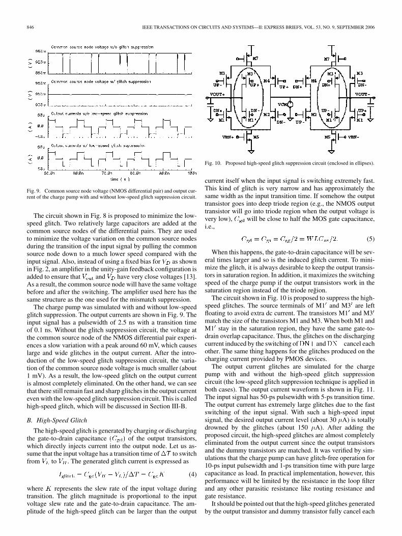
846 IEEE TRANSACTIONS ON CIRCUITS AND SYSTEMS—II: EXPRESS BRIEFS, VOL. 53, NO. 9, SEPTEMBER 2006
Fig. 9. Common source node voltage (NMOS differential pair) and output cur-rent of the charge pump with and without low-speed glitch suppression circuit.
The circuit shown in Fig. 8 is proposed to minimize the low-speed glitch. Two relatively large capacitors are added at thecommon source nodes of the differential pairs. They are usedto minimize the voltage variation on the common source nodesduring the transition of the input signal by pulling the commonsource node down to a much lower speed compared with theinput signal. Also, instead of using a fixed bias for as shownin Fig. 2, an amplifier in the unity-gain feedback configuration isadded to ensure that and have very close voltages [13].As a result, the common source node will have the same voltagebefore and after the switching. The amplifier used here has thesame structure as the one used for the mismatch suppression.
The charge pump was simulated with and without low-speedglitch suppression. The output currents are shown in Fig. 9. Theinput signal has a pulsewidth of 2.5 ns with a transition timeof 0.1 ns. Without the glitch suppression circuit, the voltage atthe common source node of the NMOS differential pair experi-ences a slow variation with a peak around 60 mV, which causeslarge and wide glitches in the output current. After the intro-duction of the low-speed glitch suppression circuit, the varia-tion of the common source node voltage is much smaller (about1 mV). As a result, the low-speed glitch on the output currentis almost completely eliminated. On the other hand, we can seethat there still remain fast and sharp glitches in the output currenteven with the low-speed glitch suppression circuit. This is calledhigh-speed glitch, which will be discussed in Section III-B.
B. High-Speed Glitch
The high-speed glitch is generated by charging or dischargingthe gate-to-drain capacitance of the output transistors,which directly injects current into the output node. Let us as-sume that the input voltage has a transition time of to switchfrom to . The generated glitch current is expressed as
(4)
where represents the slew rate of the input voltage duringtransition. The glitch magnitude is proportional to the inputvoltage slew rate and the gate-to-drain capacitance. The am-plitude of the high-speed glitch can be larger than the output
Fig. 10. Proposed high-speed glitch suppression circuit (enclosed in ellipses).
current itself when the input signal is switching extremely fast.This kind of glitch is very narrow and has approximately thesame width as the input transition time. If somehow the outputtransistor goes into deep triode region (e.g., the NMOS outputtransistor will go into triode region when the output voltage isvery low), will be close to half the MOS gate capacitance,i.e.,
(5)
When this happens, the gate-to-drain capacitance will be sev-eral times larger and so is the induced glitch current. To mini-mize the glitch, it is always desirable to keep the output transis-tors in saturation region. In addition, it maximizes the switchingspeed of the charge pump if the output transistors work in thesaturation region instead of the triode region.
The circuit shown in Fig. 10 is proposed to suppress the high-speed glitches. The source terminals of M1 and M3 are leftfloating to avoid extra dc current. The transistors M1 and M3match the size of the transistors M1 and M3. When both M1 andM1 stay in the saturation region, they have the same gate-to-drain overlap capacitance. Thus, the glitches on the dischargingcurrent induced by the switching of and cancel eachother. The same thing happens for the glitches produced on thecharging current provided by PMOS devices.
The output current glitches are simulated for the chargepump with and without the high-speed glitch suppressioncircuit (the low-speed glitch suppression technique is applied inboth cases). The output current waveform is shown in Fig. 11.The input signal has 50-ps pulsewidth with 5-ps transition time.The output current has extremely large glitches due to the fastswitching of the input signal. With such a high-speed inputsignal, the desired output current level (about 30 A) is totallydrowned by the glitches (about 150 A). After adding theproposed circuit, the high-speed glitches are almost completelyeliminated from the output current since the output transistorsand the dummy transistors are matched. It was verified by sim-ulations that the charge pump can have glitch-free operation for10-ps input pulsewidth and 1-ps transition time with pure largecapacitance as load. In practical implementation, however, thisperformance will be limited by the resistance in the loop filterand any other parasitic resistance like routing resistance andgate resistance.
It should be pointed out that the high-speed glitches generatedby the output transistor and dummy transistor fully cancel each

CHENG et al.: DESIGN AND ANALYSIS OF AN ULTRAHIGH-SPEED GLITCH-FREE FULLY DIFFERENTIAL CHARGE PUMP 847
Fig. 11. Output current with and without suppression of high-speed glitch.
Fig. 12. Complete schematic of the proposed fully differential charge pump.
other only when both of them stay in the saturation region. Theoutput voltage ranges for the NMOS and PMOS transistors tostay saturated are given below, respectively, as
(6)
where is the input signal swing. The range for the glitchesgenerated by NMOS and PMOS transistors to be fully cancelledis the cross-set of the two ranges as given as
(7)
The length of this range is given by
(8)
The simulated range of full cancellation in this design is from1.2 to 2 V with V. That’s very close to the resultestimated by (7).
IV. COMPLETE IMPLEMENTATION OF THE CHARGE PUMP
The complete schematic of the fully differential charge pumpemploying all of the techniques discussed above is shown in
Fig. 12. The overall power consumption is around 1 mW witha 3.3-V supply voltage. Simulation results indicate that thesetechniques can be combined to achieve optimum performancewithout interfering with each other.
A 10-GHz PLL with 312.5-MHz reference (modeled inCadence VerilogAMS) using the proposed charge pump wassimulated to verify system-level performance improvement.After introducing the proposed techniques, the reference spuris reduced from to dB for small differential outputvoltage of 0.4 V. Also, the spur decreases from to dBfor a large differential output voltage of 2 V.
V. CONCLUSION
A glitch-free fully differential charge pump with excellentsuppression of output current mismatch and variation is in-troduced in this study. Techniques are proposed to eliminatethe low-speed glitches caused by the speed limitation of thecommon source nodes and the high-speed glitches induced bycapacitive coupling. Especially, the technique to suppress thehigh-speed glitch enables the charge pump to have glitch-freeoperation with very narrow input pulses. Mismatch suppressioncircuit is incorporated into the proposed charge pump so thatthe output currents have very good matching over a large outputswing. Variation suppression circuit is employed to effectivelyminimize the variation of the output current amplitude with thechange of the output voltage, which results in more stable loopbandwidth of the PLL.
Detailed analysis and simulation results indicate that the pro-posed fully differential charge pump is very suitable to be usedin high-performance PLLs and CDRs working at the frequencyof multigigahertz or even higher.
REFERENCES
[1] W. Rhee, “Design of high-performance CMOS charge pumps in phase-locked loops,” in Proc. Int. Symp. Circuits Syst., May–Jun. 1999, vol.2, pp. 545–548.
[2] E. Juarez-Hernandez and A. Diaz-Sanchez, “A novel CMOS charge-pump circuit with positive feedback for PLL applications,” in Proc.Int. Conf. Electron., Circuits Syst., Sep. 2001, vol. 1, pp. 349–352.
[3] B. Bahreyni and I. M. Filanovsky, “A novel design for deadzone-lessfast charge pump with low harmonic content at the output,” in Proc.Midwest Symp. Circuits Syst., Aug. 2002, vol. 3 , pp. III-397–III-400.
[4] R. C. H. Beek and C. S. Vaucher, “A 2.5–10-GHz clock multiplierunit with 0.22-ps RMS jitter in standard 0.18-�m CMOS,” IEEE J.Solid-State Circuits, vol. 39, no. 11, pp. 1862–1872, Nov. 2004.
[5] J. F. Parker and D. Weinlader, “A 15 mW 3.125 GHz PLL for serialbackplane transceivers in 0.13 �m CMOS,” in Proc. Int. Solid-StateCircuits Conf., 2005, pp. 412–413.
[6] D. M. W. Leenaerts and J. v. der Tang, Circuit Design for RF Trans-ceivers. Boston, MA: Kluwer, 2001, ch. 7.
[7] T. S. Cheung and B. C. Lee, “A 1.8–3.2-GHz fully differential GaAsMESFET PLL,” IEEE J. Solid-State Circuits, vol. 36, no. 4, pp.605–601, Apr. 2001.
[8] N. D. Dalt and C. Sandner, “A Subpicosecond Jitter PLL for ClockGeneration in 0.12 �m Digital CMOS,” IEEE J. Solid-State Circuits,vol. 38, no. 7, pp. 1275–1278, Jul. 2003.
[9] B. Terlemez and J. P. Uyemura, “The design of a differential CMOScharge pump for high performance phase-locked loops,” in Proc. Int.Symp. Circuits Syst., May 2004, vol. 4, pp. IV–561-4.
[10] B. Razavi, Design of Analog CMOS Integrated Circuits. New York:McGraw-Hill, 2001, ch. 15, pp. 550–556.
[11] J.-S. Lee and M.-S. Keel, “Charge pump with perfect current matchingcharacteristics in phase-locked loops,” Electron. Lett., vol. 36, pp.1907–1908, Nov. 2000.
[12] J. N. Babanezhad, “A rail-to-rail CMOS op amp,” IEEE J. Solid-StateCircuits, vol. 23, no. 12, pp. 1414–1417, Dec. 1988.
[13] I. A. Young and J. K. Greason, “A PLL clock generator with 5 to 10MHz of lock range for microprocessors,” IEEE J. Solid-State Circuits,vol. 27, no. 11, pp. 1599–1607, Nov. 1992.