digital interfaces for hdtv studio signals - tt · digital interfaces for hdtv studio signals...
TRANSCRIPT

Rec. ITU-R BT.1120-4 1
RECOMMENDATION ITU-R BT.1120-4
Digital interfaces for HDTV studio signals (Question ITU-R 42/6)
(1994-1998-2000-2003)
The ITU Radiocommunication Assembly,
considering
a) that in the scope of Recommendation ITU-R BT.709, studio standards for HDTV have been developed for 1125- and 1250- line systems, which comprise systems related to conventional television as well as systems with the square pixel common image format (CIF) including progressive scanning;
b) that Recommendation ITU-R BT.709 contains the following HDTV studio standards to cover a wide range of applications:
for systems related to conventional television:
– 1125 total line, 2:1 interlace scanning, 60 fields/s, 1035 active line standard;
– 1250 total line, 2:1 interlace scanning, 50 fields/s, 1152 active line standard.
for systems with CIF (1920 × 1080):
– 1125 total lines and 1080 active lines;
– picture rates of 60, 50, 30, 25 and 24 Hz, including progressive, interlace and segmented frame transport;
c) that in Recommendation ITU-R BT.709, the 1920 × 1080 HD-CIF is given as a preferred format for new installations, where interoperability with other applications is important, and work is being directed with the aim of reaching a unique worldwide standard;
d) that the HD-CIF systems provide a common data rate feature, which allows for the use of a unique digital interface;
e) that a whole range of equipment based on the above systems has been developed or is being developed and is commercially available now or soon, including all that necessary for broadcasting chains and for industrial applications;
f) that many programmes are being produced in the above systems using the above equipments and that in the development of broadcasting and other services there is an increasing need for HDTV production installations;
g) that the use of digital technology and digital interconnection is highly desirable to reach and maintain the level of performance required for HDTV;
h) that there are clear advantages for establishing interface specifications for HDTV production installations,
recommends
1 that the specifications described in this Recommendation should be used for the basic digital coding as well for the bit-parallel and bit-serial interfaces for HDTV studio signals.

2 Rec. ITU-R BT.1120-4
PART 1
Interfaces for HDTV signals conforming to Recommendation ITU-R BT.709, Part 1
1 Digital representation
1.1 Coding characteristics
The signals to be digitized should comply with the characteristics described in Recommendation ITU-R BT.709, Part 1.
1.2 Construction of digital signals
See Part 2, § 1.2.
TABLE 1
Digital coding parameters
Value Item
Parameter
1125/60/2:1 1250/50/2:1
1 Coded signals Y, CB, CR ou R, G, B These signals are obtained from gamma pre-corrected signals, namely BGRCRCBY EEEEEE ′′′′′′ ,,or,,
Also see Recommendation ITU-R BT.709, Part 1
2 Sampling lattice
– R, G, B, Y
Orthogonal, line and picture repetitive
3 Sampling lattice
– CB, CR
Orthogonal, line and picture repetitive, co-sited with each other and with alternate Y samples. The first active colour-difference samples are co-sited with the first active Y sample
4 Number of active lines 1035 1152
5 Sampling frequency (1)
– R, G, B, Y (MHz)
74.25
72
6 Sampling frequency (1)
– CB, CR
Half of luminance sampling frequency
7 Number of samples/line
– R, G, B, Y
– CB, CR
2200
1100
2304
1152
8 Number of active samples/line
– R, G, B, Y
– CB, CR
1920
960
9 Position of the first active Y, CB, CR sampling instants with respect to the analogue sync timing reference OH
(2) (see Fig. 6)
192 T 256 T
10 Coding format Uniformly quantized PCM for each of the video component signals 8 or 10 bit/sample 10 bit preferable
Rec. ITU-R BT.1120-4 3
TABLE 1 (end )
2 Digital interface The interface provides a unidirectional interconnection between a single source and a single destination. The data signals are in the form of binary information and are coded accordingly: – video data (8-bit or 10-bit words); – timing reference and identification codes (8-bit or 10-bit words except for 1250/50/2:1,
which use 10-bit words only); – ancillary data (see Recommendation ITU-R BT.1364).
2.1 Video data Y, CB, CR signals are handled as 20-bit words by time-multiplexing CB and CR components. Each 20-bit word corresponds to a colour-difference sample and a luminance sample. The multiplex is organized as:
(CB1 Y1) (CR1 Y2) (CB3 Y3) (CR3 Y4) ...
where Yi indicates the i-th active sample of a line, while CBi and CRi indicate the colour-difference samples of CB and CR components co-sited with the Yi sample. Note that the index “i” on colour-difference samples takes only odd values due to the half-rate sampling of the colour-difference signals.
The data words corresponding to digital levels 0.00 through 0.75 and 255.00 through 255.75 are reserved for data identification purposes and must not appear as video data.
For 1125/60/2:1, R, G, B signals are handled as 30-bit words in addition to the above 20-bit words for Y, CB, CR signals.
Value Item
Parameter
1125/60/2:1 1250/50/2:1
11 Quantization level assignment (3)
– Video data
– Timing reference
1.00 through 254.75
0.00 and 255.75
(4)
12 Quantization levels (5)
– Black level R, G, B, Y
– Achromatic level CB, CR
– Nominal peak
– R, G, B, Y
CB, CR
16.00
128.00
235.00
16.00 and 240.00
13 Filter characteristics See Recommendation ITU-R BT.709 (1) The sampling clock must be locked to the line frequency. The tolerance on frequency is ±0.001% for 1125/60/2:1 and
±0.0001% for 1250/50/2:1, respectively. (2) T denotes the duration of the luminance sampling clock or the reciprocal of the luminance sampling frequency. (3) To reduce confusion when using 8-bit and 10-bit systems together, the two LSBs of the 10-bit system are read as two fractional
bits. The quantization scale in an 8-bit system ranges from 0 to 255 in steps of 1, and in a 10-bit system from 0.00 to 255.75 in steps of 0.25. When 8-bit words are presented in a 10-bit system, two LSBs of zeros are to be appended to the 8-bit words.
(4) In the case of a 8-bit system, eight MSBs are used. (5) These levels refer to precise nominal video levels. Signal processing may occasionally cause the signal level to deviate outside
these ranges.

4 Rec. ITU-R BT.1120-4
2.2 Video timing relationship with analogue waveform
The digital line occupies m clock periods. It begins at f clock periods prior to the reference transition (OH) of the analogue synchronizing signal in the corresponding line. The digital active line begins at g clock periods after the reference transition (OH). The values for m, f and g are listed in Table 2. See Fig. 6 and Table 2 for detailed timing relationships in the line interval.
The start of digital field is fixed by the position specified for the start of the digital line. See Fig. 1 and Table 3 for detailed relationships in the field interval.
TABLE 2
Line interval timing specifications
2.3 Video timing reference codes (SAV and EAV)
There are two timing reference codes, one at the beginning of each video data block (start of active video, SAV) and the other at the end of each video data block (end of active video, EAV). These codes are contiguous with the video data, and continue during the field/frame blanking interval, as shown in Fig. 1.
Value Symbol
Parameter
1125/60/2:1 1250/50/2:1
Interlace ratio 2:1
Number of active Y samples per line 1920
Luminance sampling frequency (MHz) 74,25 72
a Analogue line blanking (µs) 3.771 6.00
b Analogue active line (µs) 25.859 26.00
c Analogue full line (µs) 29.630 32.00
d Duration between end of analogue active video and start of EAV (T)
0-6 24
e Duration between end of SAV and start of analogue active video (T)
0-6 24
f Duration between start of EAV and analogue timing reference OH (T)
88 128
g Duration between analogue timing reference OH and end of SAV (T)
192 256
h Video data block (T) 1928
i Duration of EAV (T) 4
j Duration of SAV (T) 4
k Digital line blanking (T) 280 384
l Digital active line (T) 1920
m Digital line (T) 2200 2304
NOTE 1 – The parameter values for analogue specifications expressed by the symbols a, b and c indicate the nominal values.
NOTE 2 – T denotes the duration of the luminance sampling clock or the reciprocal of the luminance sampling frequency.

Rec. ITU-R BT.1120-4 5
Each code consists of a four-word sequence. The bit assignment of the word is given in Table 14. The first three words are the fixed preamble and the fourth word carries the information that defines field identification (F), field/frame blanking period (V), and line blanking period (H). In an 8-bit implementation bits Nos. 9 to 2 inclusive are used; note in 1250/50/2:1 all 10 bits are required.
The bits F and V change state synchronously with EAV at the beginning of the digital line.
The value of protection bits, P0 to P3, depends on the F, V and H as shown in Table 15. The arrangement permits one-bit errors to be corrected and two-bit errors to be detected at the receiver, but only in the 8 MSBs, as shown in Table 16.
1120-01
02
2
02
26
64
46
6
L1
L2L3
L4L5
L6L7
L8L9
L10L11
L127
75
57
73
31
13
3
Digital line blanking
EAV SAV
1 fr
ame
Fiel
d N
o. 1
Fiel
d N
o. 2
Field No. 1active video
Field No. 2active video
Value of (F/V/H) Value of (F/V/H)
1 digital line
Note 1 – The values of (F/V/H) for EAV and SAV represent the status of bits for F, V, and H; in a way that thethree-bit word composed of F, V, H represents a binary number expressed in decimal notation (F correspondingto MSB and H to LSB). For example, the value 3 represents the bits of F = 0, V = 1 and H = 1.
FIGURE 1Field timing relationship

6 Rec. ITU-R BT.1120-4
TABLE 3
Field interval timing specifications
2.4 Ancillary data
See Part 2, § 2.4.
2.5 Data words during blanking
See Part 2, § 2.5.
3 Bit-parallel interface
For the system of 1125/60/2:1, the bits of the digital code words which describe the video signal are transmitted in parallel by means of 20 or 30 shielded conductor pairs. The 20 conductor pairs are used for the transmission of the signal set consisting of luminance Y and time-multiplexed colour-difference CB/CR components. The 30 conductor pairs are used for the transmission of R, G, B signals or Y, CB/CR components with an additional data stream (auxiliary channel). An additional shielded conductor pair carries the synchronous clock at 74.25 MHz.
Digital line number Symbol
Definition
1125/60/2:1 1250/50/2:1
Number of active lines 1035 1152
L1 First line of field No. 1 1
L2 Last line of digital field blanking No. 1 40 44
L3 First line of field No. 1 active video 41 45
L4 Last line of field No. 1 active video 557 620
L5 First line of digital field blanking No. 2 558 621
L6 Last line of field No. 1 563 625
L7 First line of field No. 2 564 626
L8 Last line of digital field blanking No. 2 602 669
L9 First line of field No. 2 active video 603 670
L10 Last line of field No. 2 active video 1120 1245
L11 First line of digital field blanking No. 1 1121 1246
L12 Last line of field No. 2 1125 1250
NOTE 1 – Digital field blanking No. 1 denotes the field blanking period that is prior to the active video of field No. 1, and digital field blanking No. 2 denotes that prior to the active video of field No. 2.
Rec. ITU-R BT.1120-4 7
For the 1250/50/2:1 system, the bits of digital code words that describe the video signal are transmitted in parallel by means of 20 signal pairs, where each pair carries a stream of bits, 10 pairs for luminance data and 10 pairs for time-multiplexed colour-difference data. The 20 pairs can also carry ancillary data. A 21st pair provides a synchronous clock at 36 MHz.
Data signals are transmitted in non-return-to-zero (NRZ) form in real time (unbuffered).
3.1 Clock signal and clock-to-data timing relationship
For the system of 1125/60/2:1, the transmitted clock signal is a square wave, of which positive transitions occur midway between the data transitions as shown in Fig. 8 and Table 4.
For 1250/50/2:1, the transmitted clock signal is a 36 MHz square wave of unity mark/space ratio, the transitions of which are coincident with the transition of the data (see Fig. 2). A logical high state of the clock is concurrent with Y and CB data samples and a logical low state with Y and CR data samples, as shown in Fig. 2 and Table 4.
TABLE 4
Clock signal specifications
Value Parameter
1125/60/2:1 1250/50/2:1
Sampling frequency for Y, R, G, B signals (MHz) 74.25 72
Clock period Tck
Nominal value (ns)
1/(2200 fH)
13.468
1/(1152 fH)
27.778
Clock pulse width, t 0.5 Tck
Tolerance ±0.11 Tck (nominal)
Clock jitter Within ±0.04 Tck Within ±0.5 ns
from the average time of transition over one field in interlace systems, and over one frame in progressive systems
Data timing, Td
Tolerance
0.5 Tck
±0.075 Tck
0.25 Tck
(nominal)
NOTE 1 – fH denotes the line frequency. NOTE 2 – Values are specified at the sending end (source).

8 Rec. ITU-R BT.1120-4
1120-02
t
Y1 CB1 Y2 CR1 CB3Y3
FIGURE 2Clock to data timing relationship for 1250/50/2:1
Clock
Data
Nominal data detection points
Tck
TdTd
3.2 Electrical characteristics of the interface
The interface employs 21 line drivers and line receivers, in the case of the transmission of Y and CB/CR components. Each line driver has a balanced output and the corresponding line receiver has a balanced input. For 1125/60/2:1, the interface employs 31 line drivers and line receivers, in the case of R, G and B components or Y, CB/CR with an additional data stream (auxiliary channel).
Although the use of ECL technology is not mandatory, the line driver and receiver must be ECL 10 k compatible for 1125/60/2:1, and ECL 100 k compatible for 1250/50/2:1, i.e. they must permit the use of ECL for either drivers or receivers.
The receiver must sense correctly the data when a random signal produces conditions represented by the eye diagram of Fig. 3.

Rec. ITU-R BT.1120-4 9
TABLE 5
Line driver characteristics
TABLE 6
Line driver characteristics
Value Item
Parameter
1125/60/2:1 1250/50/2:1
1 Output impedance (Ω) 110 maximum 100 maximum
2 Common mode voltage (1) (V) –1.29 ± 15% –1.3 ± 15%
3 Signal amplitude(2) (V) 0.6 to 2.0 p-p 0.8 to 2.0 p-p
4 Rise and fall times (3) ≤ 0.15 Tck < 3 ns
5 Difference between rise and fall times ≤ 0.075 Tck ≤ 1.0 ns
NOTE 1 – Tck denotes the clock period (see Table 4). (1) Measured relative to ground. (2) Measured across a resistive load having the nominal impedance of the assumed cables, that is 110 Ω for 1125/60/2:1, and
100 Ω for 1250/50/2:1. (3) Measured between the 20% and 80% points across a resistive load having the nominal impedance of the assumed cable.
Value Item
Parameter
1125/60/2:1 1250/50/2:1
1 Input impedance (Ω) 110 ± 10% 100 ± 10%
2 Maximum input signal voltage (V) 2.0 p-p
3 Minimum input signal voltage (mV) 185 p-p
4 Maximum common mode voltage (1) (V) ±0.3 ±0.5
5 Differential delay Tmin (2) 0.3 Tck 4.5 ns
NOTE 1 – Tck denotes the clock period (see Table 4). (1) Comprising interference in the range DC to line frequency (fH). (2) Data must be correctly sensed when the differential delay between the received clock and data is within this range (see Fig. 3).
10 Rec. ITU-R BT.1120-4
1120-03
FIGURE 3Idealized eye diagram corresponding
to the minimum input signal level
Reference transitionof clock
Note 1 – For 1125/60/2:1, the width of the window in the eye diagram,within which data must be correctly detected, comprises ±0.04 Tclock jitter, ±0.075 T data timing, and ±0.18 T propagation skewof conductor pairs. For 1250/50/2:1, the aggregate of clock jitter, data timing andpropagation skew of conductor pairs must not exceed 4.5 ns.
Tmin Tmin
Vmin
3.3 Mechanical characteristics
3.3.1 Connector
The interface uses a multi-contact connector. Connectors are locked by two screws on the cable connectors and two threaded bolts on the equipment. Cable connectors employ pin contacts and equipment connectors employ socket contacts. Shielding of the connectors and cables is mandatory.
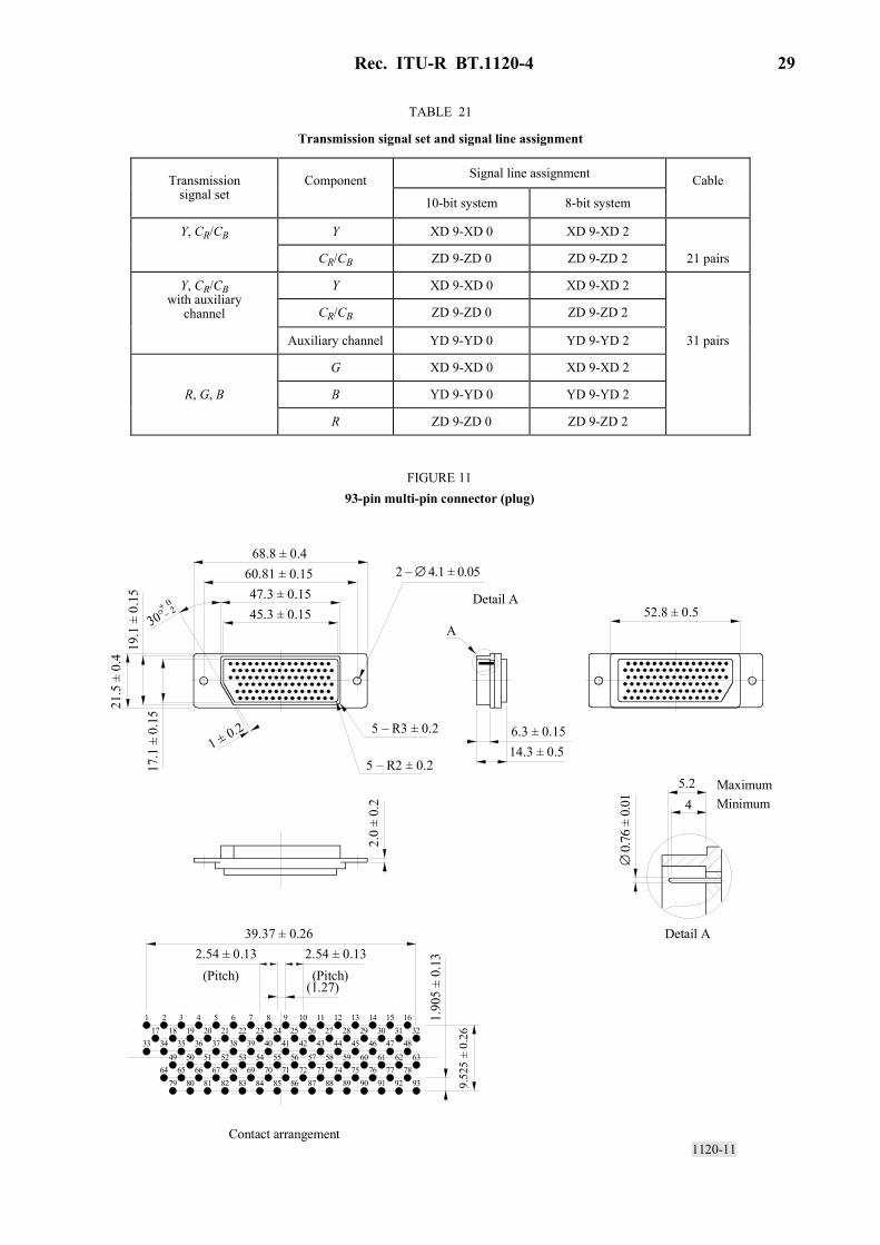
For 1125/60/2:1, a 93-contact connector is used. Contact assignments are indicated in Tables 20 and 21. The mechanical specifications for the connectors are shown in Figs. 11, 12 and 13.
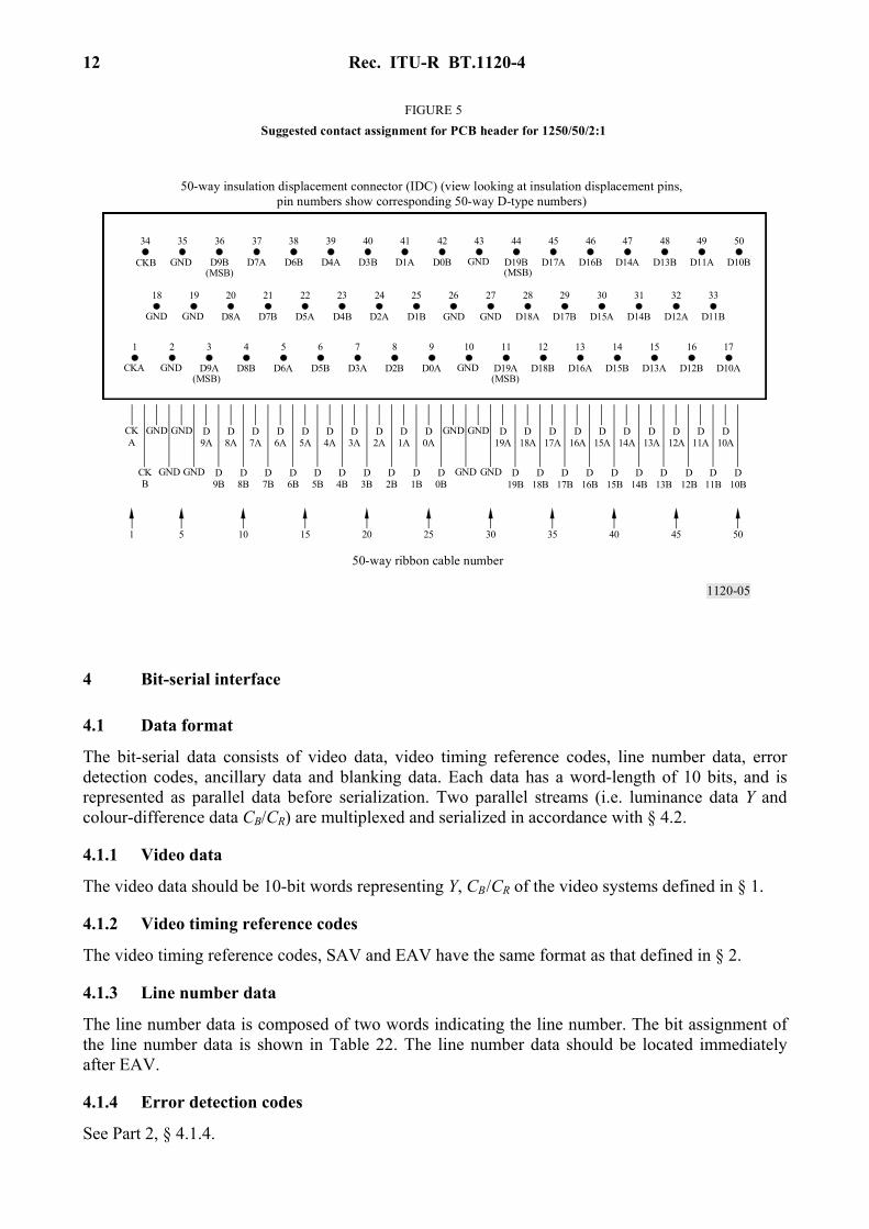
For 1250/50/2:1, a 50-contact type D subminiature connector is used. Contact assignments are indicated in Table 7 and Fig. 4 (for information, suggested contact assignment for a printed circuit board (PCB) header are shown in Fig. 5).
3.3.2 Interconnecting cable
For 1125/60/2:1, two types of multichannel cable, either 21 or 31 channels, can be used in accordance with the transmission signal set (see Table 21). The cable consists of twisted pairs with an individual shield for each pair. It also contains an overall shield. The nominal characteristic impedance of each twisted pair is 110 Ω. The cable shall possess the characteristics that satisfy the conditions of the eye diagram shown in Fig. 3 up to a maximum cable length of 20 m.
Rec. ITU-R BT.1120-4 11
For 1250/50/2:1, a cable with 21-channel balanced conductor pairs is used. The nominal characteristic impedance of each conductor pair is 100 Ω. Cable length up to 30 m may be employed when a high-quality cable is used.
TABLE 7
Connector contact assignment for 1250/50/2:1
1120-04
1 2 3 4 5 6 7 8 9 10 11 12 13 14 15 16 17
18 19 20 21 22 23 24 25 26 27 28 29 30 31 32 33
34 35 36 37 38 39 40 41 42 43 44 45 46 47 48 49 50
FIGURE 4Mating face of connector receptacle containing male pins (plug) for 1250/50/2:1
Note 1 – The preferred orientation for connectors, mounted vertically or horizontally, is with contact 1 uppermost.
Contact Signal line Contact Signal
line Contact Signal line
1 Clock A (CKA) 34 Clock B
2 GND 18 GND 35 GND
3 Data 9A (D9A) 19 GND 36 Data 9B
4 Data 8B 20 Data 8A 37 Data 7A
5 Data 6A 21 Data 7B 38 Data 6B
6 Data 5B 22 Data 5A 39 Data 4A
7 Data 3A 23 Data 4B 40 Data 3B
8 Data 2B 24 Data 2A 41 Data 1A
9 Data 0A 25 Data 1B 42 Data 0B
10 GND 26 GND 43 GND
11 Data 19A 27 GND 44 Data 19B
12 Data 18B 28 Data 18A 45 Data 17A
13 Data 16A 29 Data 17B 46 Data 16B
14 Data 15B 30 Data 15A 47 Data 14A
15 Data 13A 31 Data 14B 48 Data 13B
16 Data 12B 32 Data 12A 49 Data 11A
17 Data 10A 33 Data 11B 50 Data 10B
NOTE 1 – Data 9-Data 0 represent each bit of the luminance signal (Y ), and Data 19-Data 10 that of time-multiplexed colour-difference signal (CR /CB ). The suffix 19 to 0 indicates the bit number (bit 19 denotes MSB for CR/CB and bit 9 MSB for Y ). A and B correspond to the terminals A and B of Fig. 9, respectively.
12 Rec. ITU-R BT.1120-4
1120-05
1 2 3 4 5 6 7 8 9 10 11 12 13 14 15 16 17
5034 35 36 37 38 39 40 41 42 43 44 45 46 47 48 49
D10BD9B D7A D6B D4A D3B D1A D0B D19B D17A D16B D14A D13B D11A
18 19 20 21 22 23 24 25 26 27 28 29 30 31 32 33
D8A D7B D5A D4B D2A D1B D18A D17B D15A D14B D12A D11B
D9A D8B D6A D5B D3A D2B D0A D19A D18B D16A D15B D12B D10AD13A
1 5 10 15 20 25 30 35 40 45 50
D9A
D8A
D7A
D6A
D5A
D4A
D3A
D2A
D1A
D0A
D19A
D18A
D17A
D16A
D15A
D14A
D13A
D12A
D11A
D10A
D9B
D8B
D7B
D6B
D5B
D4B
D3B
D2B
D1B
D0B
D19B
D18B
D17B
D16B
D15B
D14B
D13B
D12B
D11B
D10B
FIGURE 5Suggested contact assignment for PCB header for 1250/50/2:1
50-way ribbon cable number
50-way insulation displacement connector (IDC) (view looking at insulation displacement pins,pin numbers show corresponding 50-way D-type numbers)
CKB GND(MSB)
(MSB)
(MSB)
(MSB)CKA
GND
GND
GND
GND
GND
CKA
GND GND GND GND
CKB
GND GND GND GND
GND GND
4 Bit-serial interface
4.1 Data format
The bit-serial data consists of video data, video timing reference codes, line number data, error detection codes, ancillary data and blanking data. Each data has a word-length of 10 bits, and is represented as parallel data before serialization. Two parallel streams (i.e. luminance data Y and colour-difference data CB/CR) are multiplexed and serialized in accordance with § 4.2.
4.1.1 Video data
The video data should be 10-bit words representing Y, CB /CR of the video systems defined in § 1.
4.1.2 Video timing reference codes
The video timing reference codes, SAV and EAV have the same format as that defined in § 2.
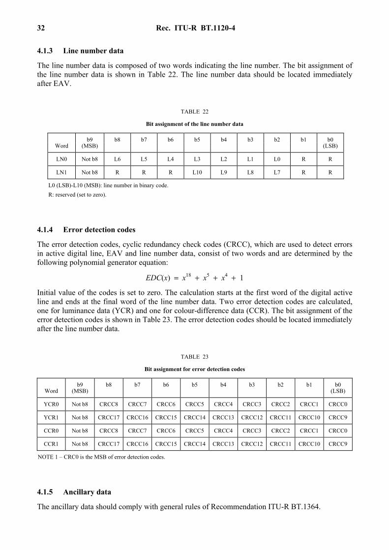
4.1.3 Line number data
The line number data is composed of two words indicating the line number. The bit assignment of the line number data is shown in Table 22. The line number data should be located immediately after EAV.
4.1.4 Error detection codes
See Part 2, § 4.1.4.

Rec. ITU-R BT.1120-4 13
4.1.5 Ancillary data
See Part 2, § 4.1.5.
4.1.6 Blanking data
See Part 2, § 4.1.6.
4.2 Transmission format
See Part 2, § 4.2.
4.2.1 Word-multiplexing
The two parallel streams should be multiplexed word by word into a single 10-bit parallel stream in the order of CB, Y, CR, Y, CB, Y, CR, Y ... (see Fig. 14 and Table 8).
TABLE 8
Data stream timing specifications (see Fig. 14)
4.2.2 Serializing
See Part 2, § 4.2.2.
4.2.3 Channel coding
See Part 2, § 4.2.3.
4.2.4 Serial clock
Table 9 specifies the serial clock frequencies, which are twenty times the frequency of the parallel clock (see Table 4).
TABLE 9
Serial clock frequency
Value Symbol
Parameter
1125/60/2:1 1250/50/2:1
T Parallel clock period (ns) 1000/74,25 1000/72 Ts Multiplexed parallel data clock period T/2 m Digital line in parallel data stream 2200 2304 k Digital line blanking in parallel data
stream 280 384
n Ancillary data or blanking data in parallel data stream
268 372
ms Digital line in multiplexed parallel data stream
4400 4608
ks Digital line blanking in multiplexed parallel data stream
560 768
ns Ancillary data or blanking data in multiplexed parallel data stream
536 744
Value Parameter
1125/60/2:1 1250/50/2:1
Serial clock frequency (GHz) 1.485 1.400

14 Rec. ITU-R BT.1120-4
4.2.5 Bit-serial digital check field See Part 2, § 4.2.5.
4.3 Coaxial cable interfaces See Part 2, § 4.3.
4.3.1 Line driver characteristics (source) See Part 2, § 4.3.1.
4.3.2 Line receiver characteristics (destination) See Part 2, § 4.3.2.
4.3.3 Transmission line characteristics See Part 2, § 4.3.3.
4.3.4 Connector See Part 2, § 4.3.4.
4.4 Optical fibre interfaces See Part 2, § 4.4.
PART 2
Interfaces for HDTV signals conforming to Recommendation ITU-R BT.709, Part 2
This part specifies digital interfaces for the systems listed in Table 10. For the 60, 30 and 24 Hz systems, picture rates having those values divided by 1.001 are also included. Parameter values for these systems are presented in parentheses.
TABLE 10
HDTV systems based on CIF (see Recommendation ITU-R BT.709, Part 2)
System Capture (Hz) Transport
60/P 60 progressive Progressive
30/P 30 progressive Progressive
30/PsF 30 progressive Segmented frame
60/I 30 interlace Interlace
50/P 50 progressive Progressive
25/P 25 progressive Progressive
25/PsF 25 progressive Segmented frame
50/I 25 interlace Interlace
24/P 24 progressive Progressive
24/PsF 24 progressive Segmented frame

Rec. ITU-R BT.1120-4 15
1 Digital representation
1.1 Coding characteristics The signals to be digitized should comply with the characteristics described in Recommendation ITU-R BT.709, Part 2.
1.2 Construction of digital signals Digital representation of R, G, B, Y, CR and CB may be obtained using the following relationship. Further study is required in terms of conversion between the data obtained with 8-bit and 10-bit quantization.
Rd = [ Int ( 219 × D ) × RE′ + ( 16 × D ) + 0.5 ] / D
Gd = [ Int ( 219 × D ) × GE′ + ( 16 × D ) + 0.5 ] / D
Bd = [ Int ( 219 × D ) × BE′ + ( 16 × D ) + 0.5 ] / D
Yd = [ Int ( 219 × D ) × YE′ + ( 16 × D ) + 0.5 ] / D
CBd = [ Int ( 224 × D ) × BCE′ + ( 128 × D ) + 0.5 ] / D
CRd = [ Int ( 224 × D ) × RCE′ + ( 128 × D ) + 0.5 ] / D
where D takes either the value 1 or 4, corresponding to 8-bit or 10-bit quantization respectively; GE′ , BE′ , RE′ and YE′ denote analogue R, G, B and luminance signals that have been normalized to
span the range 0.0 to 1.0, while RCE′ and
BCE′ denote analogue colour-difference signals that have been normalized to span the range – 0.5 to +0.5.
2 Digital interface The interface provides a unidirectional interconnection between a single source and a single destination. The data signals are in the form of binary information and are coded accordingly: – video data (8-bit or 10-bit words); – timing reference and identification codes (8-bit or 10-bit words); – ancillary data (see Recommendation ITU-R BT.1364).
2.1 Video data
Y, CB and CR signals are handled as 20-bit words by time-multiplexing CB and CR components. Each 20-bit word corresponds to a colour-difference sample and a luminance sample. The multiplex is organized as:
(CB1 Y1) (CR1 Y2) (CB3 Y3) (CR3 Y4) ...
where Yi indicates the i-th active sample of a line, while CBi and CRi indicate the colour-difference samples of CB and CR components co-sited with the Yi sample. Note that the index i on colour-difference samples takes only odd values due to the half-rate sampling of the colour-difference signals.
The data words corresponding to digital levels 0.00 through 0.75 and 255.00 through 255.75 are reserved for data identification purposes and must not appear as video data.
R, G, B signals are handled as 30-bit words in addition to the above 20-bit words for Y, CB, CR signals.

16 R
ec. ITU
-R B
T.1120-4
TABLE 11
Digital coding parameters
Item Parameter System
60/P 30/P 30/PsF 60/I 50/P 25/P 25/PsF 50/I 24/P 24/PsF
1 Coded signals Y, CB, CR or R, G, B These signals are obtained from gamma pre-corrected signals, namely E'Y, E'CB, E'CR or E'R, E'G, E'B. Also see Recommendation ITU-R BT.709, Part 2
2 Sampling lattice – R, G, B, Y
Orthogonal, line and picture repetitive
3 Sampling lattice – CB, CR
Orthogonal, line and picture repetitive, co-sited with each other and with alternate
(1) Y samples
4 Number of active lines 1080
5 Sampling frequency (2) (MHz) – R, G, B, Y
148.5
(148.5/1.001)
74.25
(74.25/1.001)
148.5
74.25
74.25
(74.25/1.001)
– CB, CR
(3) 74.25 (74.25/1.001)
37.125 (37.125/1.001)
74.25 37.125 37.125 (37.125/1.001)
6 Number of samples/line – R, G, B, Y – CB, CR
2 200 1100
2 640 1320
2750 1375
7 Number of active samples/line – R, G, B, Y – CB, CR
1920 960
8 Position of the first active Y, CB, CR sampling instants with respect to the analogue sync timing eference OH
(4) (see Fig. 6)
192 T
R
ec. ITU
-R B
T.1120-4
17
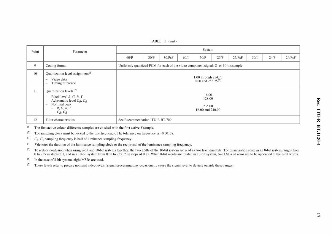
TABLE 11 (end )
Point Parameter System
60/P 30/P 30/PsF 60/I 50/P 25/P 25/PsF 50/I 24/P 24/PsF
9 Coding format Uniformly quantized PCM for each of the video component signals 8- or 10-bit/sample
10 Quantization level assignment (5)
– Video data – Timing reference
1.00 through 254.75 0.00 and 255.75
(6)
11 Quantization levels (7)
– Black level R, G, B, Y – Achromatic level CB, CR – Nominal peak – R, G, B, Y – CB, CR
16.00 128.00
235.00
16.00 and 240.00
12 Filter characteristics See Recommendation ITU-R BT.709
(1) The first active colour-difference samples are co-sited with the first active Y sample. (2) The sampling clock must be locked to the line frequency. The tolerance on frequency is ±0.001%. (3) CB, CR sampling frequency is half of luminance sampling frequency. (4) T denotes the duration of the luminance sampling clock or the reciprocal of the luminance sampling frequency. (5) To reduce confusion when using 8-bit and 10-bit systems together, the two LSBs of the 10-bit system are read as two fractional bits. The quantization scale in an 8-bit system ranges from
0 to 255 in steps of 1, and in a 10-bit system from 0.00 to 255.75 in steps of 0.25. When 8-bit words are treated in 10-bit system, two LSBs of zeros are to be appended to the 8-bit words. (6) In the case of 8-bit system, eight MSBs are used. (7) These levels refer to precise nominal video levels. Signal processing may occasionally cause the signal level to deviate outside these ranges.
18 Rec. ITU-R BT.1120-4
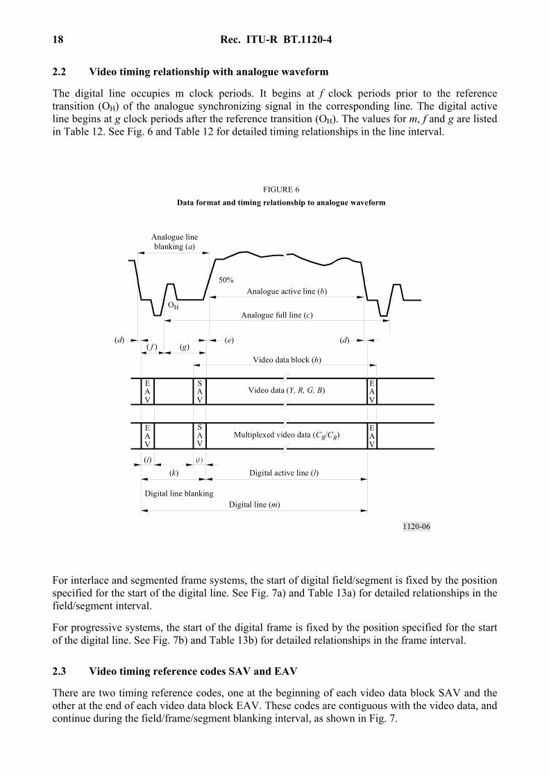
2.2 Video timing relationship with analogue waveform
The digital line occupies m clock periods. It begins at f clock periods prior to the reference transition (OH) of the analogue synchronizing signal in the corresponding line. The digital active line begins at g clock periods after the reference transition (OH). The values for m, f and g are listed in Table 12. See Fig. 6 and Table 12 for detailed timing relationships in the line interval.
1120-06
FIGURE 6Data format and timing relationship to analogue waveform
(k)
(d) (d)(e)
50%
OH
Analogue active line (b)
Analogue full line (c)
Video data block (h)( f ) (g)
EAV
SAV
EAV
Video data (Y, R, G, B)
EAV
SAV
EAV
Multiplexed video data (CB/CR)
(i)Digital active line (l)
Digital line (m)
Analogue lineblanking (a)
Digital line blanking
( )j
For interlace and segmented frame systems, the start of digital field/segment is fixed by the position specified for the start of the digital line. See Fig. 7a) and Table 13a) for detailed relationships in the field/segment interval.
For progressive systems, the start of the digital frame is fixed by the position specified for the start of the digital line. See Fig. 7b) and Table 13b) for detailed relationships in the frame interval.
2.3 Video timing reference codes SAV and EAV
There are two timing reference codes, one at the beginning of each video data block SAV and the other at the end of each video data block EAV. These codes are contiguous with the video data, and continue during the field/frame/segment blanking interval, as shown in Fig. 7.

R
ec. ITU
-R B
T.1120-4
19
TABLE 12
Line interval timing specifications
Symbol Parameter Value
60/P 30/P 30/PsF 60/I 50/P 25/P 25/PsF 50/I 24/P 24/PsF
Number of active Y samples per line 1920
Luminance sampling frequency (MHz) 148.5 (148.5/1.001)
74.25 (74.25/1.001)
148.5 74.25 74.25 (74.25/1.001)
a Analogue line blanking (T) +12 280
–0
+12 280
–0
+12 280
–0 b Analogue active line (T) +0
1920 –12
c Analogue active line (T) 2200 2640 2750 d Duration between end of analogue active video
and start of EAV (T) 0-6
e Duration between end of SAV and start of analogue active video (T)
0-6
f Duration between start of EAV and analogue timing reference OH (T)
88 528 638
g Duration between analogue timing reference OH and end of SAV (T)
192
h Video data block (T) 1928 i Duration of EAV (T) 4 j Duration of SAV (T) 4 k Digital line blanking (T) 280 720 830 l Digital active line (T) 1920 m Digital line (T) 2200 2640 2750
NOTE 1 – The parameter values for analogue specifications expressed by the symbols a, b and c indicate the nominal values. NOTE 2 – T denotes the duration of the luminance clock or the reciprocal of the luminance sampling frequency.

20 Rec. ITU-R BT.1120-4
1120-07
02
2
02
26
64
46
6
L1
L2L3
L4L5
L6L7
L8L9
L10L11
L127
75
57
73
31
13
3
02
2
02
2
L1
L2L3
L4L5
L63
31
13
3
Digital line blanking
EAV SAV
1 fr
ame
Fiel
d/se
gmen
t No.
1Fi
eld/
segm
ent N
o. 2
Field/segment No. 1active video
Field/segment No. 2active video
Value of (F/V/H) Value of (F/V/H)
1 digital line
Digital line blanking
EAV SAV
1 fr
ame
Active video
Value of (F/V/H) Value of (F/V/H)
1 digital line
a) Field/segment timing relationship for interlace and segmented frame systems
b) Frame timing relationship for progressive systems
Note 1 – The values of (F/V/H) for EAV and SAV represent the status of bits for F, V, and H; in a way that thethree-bit word composed of F, V, H represents a binary number expressed in decimal notation (F correspondingto MSB and H to LSB). For example, the value 3 represents the bits of F = 0, V = 1 and H = 1.
FIGURE 7Video timing reference codes SAV and EAV

Rec. ITU-R BT.1120-4 21
Each code consists of a four-word sequence. The bit assignment of the word is given in Table 14. The first three words are fixed preamble and the fourth word carries the information that defines field identification (F), field/frame blanking period (V), and line blanking period (H). In a 8-bit implementation bits Nos. 9 to 2 inclusive are used.
The bits F and V change state synchronously with EAV at the beginning of the digital line.
The value of protection bits, P0 to P3, depends on the F, V and H as shown in Table 15. The arrangement permits one-bit errors to be corrected and two-bit errors to be detected at the receiver, but only in the 8 MSBs, as shown in Table 16.
TABLE 13
a) Field/segment interval timing specifications for interlace and segmented frame scanning systems
b) Frame interval timing specifications for progressive systems
Symbol Definition Digital line number
Number of active lines 1080
L1 First line of field/segment No. 1 1
L2 Last line of digital field/segment blanking No. 1 20
L3 First line of field/segment No. 1 active video 21
L4 Last line of field/segment No. 1 active video 560
L5 First line of digital field/segment blanking No. 2 561
L6 Last line of field/segment No. 1 563
L7 First line of field/segment No. 2 564
L8 Last line of digital field/segment blanking No. 2 583
L9 First line of field/segment No. 2 active video 584
L10 Last line of field/segment No. 2 active video 1123
L11 First line of digital field/segment blanking No. 1 1124
L12 Last line of field/segment No. 2 1125
NOTE 1 – Digital field/segment blanking No. 1 denotes the field/segment blanking period that is prior to the active video of field/segment No. 1, and digital field/segment blanking No. 2 denotes that prior to the active video of field/segment No. 2.
Symbol Definition Digital line number
Number of active lines 1080
L1 First line of frame 1
L2 Last line of digital frame blanking 41
L3 First line of active video 42
L4 Last line of active video 1121
L5 First line of digital frame blanking 1122
L6 Last line of frame 1125

22 Rec. ITU-R BT.1120-4
TABLE 14
Bit assignment for video timing reference codes
TABLE 15
Protection bits for SAV and EAV
Word Bit number
9 (MSB)
8 7 6 5 4 3 2 1 0 (LSB)
First 1 1 1 1 1 1 1 1 1 1
Second 0 0 0 0 0 0 0 0 0 0
Third 0 0 0 0 0 0 0 0 0 0
Fourth 1 F V H P3 P2 P1 P0 0 0
Interlace and segmented frame system
F = 1 during field/segment No. 2
= 0 during field/segment No. 1
V = 1 during field/segment blanking
= 0 elsewhere
H = 1 in EAV
= 0 in SAV
Progressive system F = 0 V = 1 during frame blanking
= 0 elsewhere
H = 1 in EAV
= 0 in SAV
NOTE 1 – P0, P1, P2, P3 in the fourth word are the protection bits (see Table 15).
SAV/EAV bit status Protection bits
Bit 9 (fixed)
8 (F)
7 (V)
6 (H)
5 (P3)
4 (P2)
3 (P1)
2 (P0)
1 (fixed)
0 (fixed)
1 0 0 0 0 0 0 0 0 0
1 0 0 1 1 1 0 1 0 0
1 0 1 0 1 0 1 1 0 0
1 0 1 1 0 1 1 0 0 0
1 1 0 0 0 1 1 1 0 0
1 1 0 1 1 0 1 0 0 0
1 1 1 0 1 1 0 0 0 0
1 1 1 1 0 0 0 1 0 0

Rec. ITU-R BT.1120-4 23
TABLE 16
Error corrections using protection bits (P3-P0)
2.4 Ancillary data
Ancillary data may optionally be included in the blanking intervals of a digital interface according to this Recommendation. The ancillary signals should comply with the general rules of Recommen-dation ITU-R BT.1364.
The horizontal blanking interval between the end of EAV and the start of SAV may be employed to convey ancillary data packets.
Ancillary data packets may be conveyed in the vertical blanking interval between the end of SAV and the start of EAV as follows: − in a progressive system during lines 7 through 41 inclusive; − in an interlaced system during lines 7 through 20 inclusive and lines 569 through 583
inclusive;
Received bits 5-2
Received bits 8-6 for F, V and H
for P3-P0 000 001 010 011 100 101 110 111
0000 000 000 000 – 000 – – 111
0001 000 – – 111 – 111 111 111
0010 000 – – 011 – 101 – –
0011 – – 010 – 100 – – 111
0100 000 – – 011 – – 110 –
0101 – 001 – – 100 – – 111
0110 – 011 011 011 100 – – 011
0111 100 – – 011 100 100 100 –
1000 000 – – – – 101 110 –
1001 – 001 010 – – – – 111
1010 – 101 010 – 101 101 – 101
1011 010 – 010 010 – 101 010 –
1100 – 001 110 – 110 – 110 110
1101 001 001 – 001 – 001 110 –
1110 – – – 011 – 101 110 –
1111 – 001 010 – 100 – – –
NOTE 1 – The error correction applied provides a DEDSEC (double error detection – single error correction) function. The received bits denoted by “–” in the table, if detected, indicate that an error has occurred but cannot be corrected.

24 Rec. ITU-R BT.1120-4
− on any line that is outside the vertical extent of the picture as noted above and that is not employed to convey vertical blanking interval signals that can be represented in the analogue domain through direct (D/A) conversion (such as digital vertical interval time code (D-VITC)).
2.5 Data words during blanking
The data words occurring during digital blanking intervals that are not used for the timing reference codes (SAV and EAV), or for ancillary data (ANC) are filled with words corresponding to the following blanking levels, appropriately placed in the multiplexed data:
16.00 for Y, R, G, B signals
128.00 for CB /CR (time-multiplexed colour-difference signal).
3 Bit-parallel interface
The bits of the digital code words which describe the video signal are transmitted in parallel by means of 20 or 30 shielded conductor pairs. The 20 conductor pairs are used for the transmission of the signal set consisting of luminance Y and time-multiplexed colour-difference CB /CR components. The 30 conductor pairs are used for the transmission of R, G, B signals or Y, CB /CR components with an additional data stream (auxiliary channel). An additional shielded conductor pair carries the synchronous clock at 148.5 MHz (148.5/1.001 MHz) for 60/P and 50/P, and 74.25 MHz (74.25/1.001 MHz) for the other systems.
Data signals are transmitted in NRZ form in real time (unbuffered).
3.1 Clock signal and clock-to-data timing relationship
The transmitted clock signal is a square wave, of which positive transitions occur midway between the data transitions as shown in Fig. 8 and Table 17.
1120-08
t
Td
50%
50%
FIGURE 8Clock-to data timing relationship
Timing reference for data and clock
Clock
Data
Tck

R
ec. ITU
-R B
T.1120-4
25
TABLE 17
Clock signal specifications
Parameter Value
60/P 30/P 30/PsF 60/I 50/P 25/P 25/PsF 50/I 24/P 24/PsF
Sampling frequency for Y, R, G, B signals (MHz) 148.5 (148.5/1.001)
74.25 (74.25/1.001)
148.5 74.25 74.25 (74.25/1.001)
Clock period, Tck 1/(2200 fH) 1/(2640 fH) 1/(2750 fH)
Nominal value (ns) 6,734 (6,741)
13.468 (13.481)
6.734 13.468 13.468 (13.481)
Clock pulse width, t Tolerance
0.5 Tck ±0.11 Tck
Clock jitter Within ±0.04 Tck
from the average time of transition over one field/segment in interlace and segmented frame systems, and over one frame in progressive systems
Data timing, Td Tolerance
0.5 Tck ±0.075 Tck
NOTE 1 – fH denotes the line frequency. NOTE 2 – Values are specified at the sending end (source).

26 Rec. ITU-R BT.1120-4
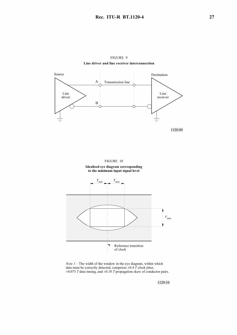
3.2 Electrical characteristics of the interface
The interface employs 21 line drivers and line receivers, in the case of the transmission of Y and CB /CR components. Each line driver has a balanced output and the corresponding line receive has a balanced input. The interface employs 31 line drivers and line receivers, in the case of R, G and B components or Y, CB /CR with an additional data stream (auxiliary channel).
Although the use of ECL technology is not mandatory, the line driver and receiver must be ECL 10 k compatible for the systems using the synchronous clock at 74.25 MHz (74.25/1.001 MHz), i.e., they must permit the use of ECL for either drivers or receivers.
The receiver must sense correctly the data when a random signal produces conditions represented by the eye diagram of Fig. 10.
TABLE 18
Line driver characteristics
TABLE 19
Line receiver characteristics
Item Parameter Value
1 Output impedance (Ω) 110 maximum
2 Common mode voltage(1) (V) –1.29 ± 15%
3 Signal amplitude(2) (V) 0.6 to 2.0 p-p
4 Rise and fall times(3) ≤ 0.15 Tck
5 Difference between rise and fall times ≤ 0.075 Tck
NOTE 1 – Tck denotes the clock period (see Table 17). (1) Measured relative to ground. (2) Measured across a resistive load having the nominal impedance of the assumed cables, that is 110 Ω. (3) Measured between the 20% and 80% points across a resistive load having the nominal impedance of the assumed cable.
Item Parameter Value
1 Input impedance (Ω) 110 ± 10
2 Maximum input signal voltage (V) 2.0 p-p
3 Minimum input signal voltage (mV) 185 p-p
4 Maximum common mode voltage(1) (V) ±0.3
5 Differential delay Tmin(2) 0.3 Tck
NOTE 1 – Tck denotes the clock period (see Table 17). (1) Comprising interference in the range DC to line frequency (fH). (2) Data must be correctly sensed when the differential delay between the received clock and data is within this range (see Fig. 10).
Rec. ITU-R BT.1120-4 27
1120-09
A
B
FIGURE 9Line driver and line receiver interconnection
Linedriver
Linereceiver
Source Destination
Transmission line
1120-10
FIGURE 10Idealized eye diagram corresponding
to the minimum input signal level
Reference transitionof clock
Note 1 – The width of the window in the eye diagram, within whichdata must be correctly detected, comprises ±0.4 T clock jitter,±0.075 T data timing, and ±0.18 T propagation skew of conductor pairs.
Tmin Tmin
Vmin

28 Rec. ITU-R BT.1120-4
3.3 Mechanical characteristics (see Note 1)
3.3.1 Connector
The interface uses a multi-contact connector. Connectors are locked by two screws on the cable connectors and two threaded bolts on the equipment. Cable connectors employ pin contacts and equipment connectors employ socket contacts. Shielding of the connectors and cables is mandatory.
A 93-contact connector is used. Contact assignments are indicated in Tables 20 and 21. The mechanical specifications for the connectors are shown in Figs. 11, 12 and 13. NOTE 1 – For new designs, bit-serial interface described in § 4 is preferred.
TABLE 20
Connector contact assignment
3.3.2 Interconnecting cable
Two types of multi-channel cable, either 21 or 31 channels, can be used in accordance with the transmission signal set (see Table 21). The cable consists of twisted pairs with an individual shield for each pair. It also contains an overall shield. The nominal characteristic impedance of each twisted pair is 110 Ω. The cable shall possess the characteristics that satisfy the conditions of the eye diagram shown in Fig. 10 up to a maximum cable length of 20 m for the system using the synchronous clock at 74.25 MHz (74.25/1.001 MHz), and 14 m for the systems using the synchronous clock at 148.5 MHz (148.5/1.001 MHz).
Con- tact
Signal line
Con- tact
Signal line
Con- tact
Signal line
Con-tact
Signal line
Con-tact
Signal line
Con- tact
Signal line
1 Clock A 17 GND 33 Clock B
2 XD 9A 18 GND 34 XD 9B 49 YD 4A 64 GND 79 YD 4B
3 XD 8A 19 GND 35 XD 8B 50 YD 3A 65 GND 80 YD 3B
4 XD 7A 20 GND 36 XD 7B 51 YD 2A 66 GND 81 YD 2B
5 XD 6A 21 GND 37 XD 6B 52 YD 1A 67 GND 82 YD 1B
6 XD 5A 22 GND 38 XD 5B 53 YD 0A 68 GND 83 YD 0B
7 XD 4A 23 GND 39 XD 4B 54 ZD 9A 69 GND 84 ZD 9B
8 XD 3A 24 GND 40 XD 3B 55 ZD 8A 70 GND 85 ZD 8B
9 XD 2A 25 GND 41 XD 2B 56 ZD 7A 71 GND 86 ZD 7B
10 XD 1A 26 GND 42 XD 1B 57 ZD 6A 72 GND 87 ZD 6B
11 XD 0A 27 GND 43 XD 0B 58 ZD 5A 73 GND 88 ZD 5B
12 YD 9A 28 GND 44 YD 9B 59 ZD 4A 74 GND 89 ZD 4B
13 YD 8A 29 GND 45 YD 8B 60 ZD 3A 75 GND 90 ZD 3B
14 YD 7A 30 GND 46 YD 7B 61 ZD 2A 76 GND 91 ZD 2B
15 YD 6A 31 GND 47 YD 6B 62 ZD 1A 77 GND 92 ZD 1B
16 YD 5A 32 GND 48 YD 5B 63 ZD 0A 78 GND 93 ZD 0B
NOTE 1 – XD 9-XD 0, YD 9-YD 0, and ZD 9-ZD 0 represent each bit of the component signals. The suffix 9 to 0 indicates the bit number (bit 9 denotes MSB). A and B correspond to the terminals A and B of Fig. 9, respectively. The relationship between XD, YD, ZD and component signals are specified in Table 21. NOTE 2 – The shield of each pair uses the ground contact (GND) located between A and B contacts for the signal, e.g., contact No. 17 is used for the shield of the clock signal. The overall shield of the cable is electrically connected to connector hood, which is grounded to the frame of the equipment.
Rec. ITU-R BT.1120-4 29
TABLE 21
Transmission signal set and signal line assignment
1120-11
A
33 34 35 36 37 38 39 40 41 42 43 44 45 46 47 4849 50 51 52 53 54 55 56 57 58 59 60 61 62 63
64 65 66 67 68 69 70 71 72 73 74 75 76 77 7879 80 81 82 83 84 85 86 87 88 89 90 91 92 93
1 2 3 4 5 6 7 8 9 10 11 12 13 14 15 1617 18 19 20 21 22 23 24 25 26 27 28 29 30 31 32
4
(1.27)
5.2
FIGURE 1193-pin multi-pin connector (plug)
Detail A
Contact arrangement
Detail A
(Pitch) (Pitch)
MaximumMinimum
68.8 ± 0.4
47.3 ± 0.1560.81 ± 0.15
45.3 ± 0.15 52.8 ± 0.5
6.3 ± 0.1514.3 ± 0.5
5 – R3 ± 0.2
5 – R2 ± 0.2
∅ 0
.76
± 0.
01
2.0
± 0.
2
21.5
± 0
.419
.1 ±
0.1
517
.1 ±
0.1
5
39.37 ± 0.262.54 ± 0.132.54 ± 0.13
1.90
5 ±
0.13
9.52
5 ±
0.26
2 – ∅ 4.1 ± 0.05
Component Signal line assignment Cable Transmission signal set 10-bit system 8-bit system
Y, CR/CB Y XD 9-XD 0 XD 9-XD 2
CR/CB ZD 9-ZD 0 ZD 9-ZD 2 21 pairs
Y XD 9-XD 0 XD 9-XD 2 Y, CR/CB with auxiliary
channel CR/CB ZD 9-ZD 0 ZD 9-ZD 2
Auxiliary channel YD 9-YD 0 YD 9-YD 2 31 pairs
G XD 9-XD 0 XD 9-XD 2
R, G, B B YD 9-YD 0 YD 9-YD 2
R ZD 9-ZD 0 ZD 9-ZD 2

30 Rec. ITU-R BT.1120-4
1120-12
33343536373839404142434445464748495051525354555657585960616263
646566676869707172737475767778798081828384858687888990919293
1234567891011121314151617181920212223242526272829303132
FIGURE 1293-pin multi-pin connector (receptacle)
Panel cutouts
(Thr
ead
leng
th)
(Pitch) (Pitch)
3.8(Note 1)
(1.27)
(Pitch)
(Pitc
h)
Contact arrangement
2 – No.6 – 32UNC – 2B
4 m
inim
um
4 – R2.8
9.525 ± 0.5
2 – M4 (P = 0.7)
6.8
– 0.
30
2 – ∅ 3.05 ± 0.05 2 – ∅ 3.8 ± 0.05
60.81 ± 0.148 ± 0.2 60.81 ± 0.2
6.5
± 0.
1
19.8
± 0
.2
2 – ∅ 6.5 ± 0.05∅ 6 ± 0.212.1
± 0
.25
22.5
± 0
.25
0.8 ± 0.156 ± 0.15
68.8 ± 0.460.81 ± 0.1547.3 ± 0.1548.8 ± 0.15
19.1
± 0
.15
21.5
± 0
.4
16.6
± 0
.15
4 – R3 ± 0.2
5 – R2.4 ± 0.2 10.195 ± 0.25 1.905 ± 0.25
∅ 0.45 ± 0.1
3.5
± 0.
5
39.37 ± 0.26
2.54 ± 0.13 2.54 ± 0.13
1.90
5 ±
0.13
9.52
5 ±
0.26

Rec. ITU-R BT.1120-4 31
1120-13
FIGURE 1393-pin multi-pin connector (hood)
(Not
e 1)
68 m
axim
um
78 maximum
2 – M4 (P = 0.7) 33 maximum Plug connector
Note 1 – A screw projecting out from the plug connector.Note 2 – Applicable outer diameter: 17.5 minimum to 19.3 maximum and 21.1 minimum to 23.2 maximum.
3.5
± 0.
4
60.81 ± 0.15
4 Bit-serial interface
Specifications for 60/P and 50/P are under study.
4.1 Data format
The bit-serial data consists of video data, video timing reference codes, line number data, error detection codes, ancillary data and blanking data. Each data has a word-length of 10 bits, and is represented as parallel data before serialization. Two parallel streams (i.e. luminance data Y and colour-difference data CB /CR) are multiplexed and serialized in accordance with § 4.2.
4.1.1 Video data
The video data should be 10-bit words representing Y, CB /CR of the video systems defined in § 1.
4.1.2 Video timing reference codes
The video timing reference codes, SAV and EAV have the same format as that defined in § 2.
32 Rec. ITU-R BT.1120-4
4.1.3 Line number data
The line number data is composed of two words indicating the line number. The bit assignment of the line number data is shown in Table 22. The line number data should be located immediately after EAV.
TABLE 22
Bit assignment of the line number data
4.1.4 Error detection codes
The error detection codes, cyclic redundancy check codes (CRCC), which are used to detect errors in active digital line, EAV and line number data, consist of two words and are determined by the following polynomial generator equation:
EDC(x) = x18 + x5 + x4 + 1
Initial value of the codes is set to zero. The calculation starts at the first word of the digital active line and ends at the final word of the line number data. Two error detection codes are calculated, one for luminance data (YCR) and one for colour-difference data (CCR). The bit assignment of the error detection codes is shown in Table 23. The error detection codes should be located immediately after the line number data.
TABLE 23
Bit assignment for error detection codes
4.1.5 Ancillary data
The ancillary data should comply with general rules of Recommendation ITU-R BT.1364.
b9 b8 b7 b6 b5 b4 b3 b2 b1 b0 Word (MSB) (LSB)
LN0 Not b8 L6 L5 L4 L3 L2 L1 L0 R R
LN1 Not b8 R R R L10 L9 L8 L7 R R
L0 (LSB)-L10 (MSB): line number in binary code. R: reserved (set to zero).
b9 b8 b7 b6 b5 b4 b3 b2 b1 b0 Word (MSB) (LSB)
YCR0 Not b8 CRCC8 CRCC7 CRCC6 CRCC5 CRCC4 CRCC3 CRCC2 CRCC1 CRCC0
YCR1 Not b8 CRCC17 CRCC16 CRCC15 CRCC14 CRCC13 CRCC12 CRCC11 CRCC10 CRCC9
CCR0 Not b8 CRCC8 CRCC7 CRCC6 CRCC5 CRCC4 CRCC3 CRCC2 CRCC1 CRCC0
CCR1 Not b8 CRCC17 CRCC16 CRCC15 CRCC14 CRCC13 CRCC12 CRCC11 CRCC10 CRCC9
NOTE 1 – CRC0 is the MSB of error detection codes.

Rec. ITU-R BT.1120-4 33
4.1.6 Blanking data
The blanking data words during digital blanking intervals that are not used for SAV, EAV, the line number data, the error detection codes and the ancillary data, should be filled with the 10-bit words corresponding to the following quantization levels:
– 16.00 for Y data
– 128.00 for CB /CR data.
4.2 Transmission format
The two parallel data streams are transmitted over a single channel in bit-serial form after word-multiplexing, parallel-to-serial conversion and scrambling.
4.2.1 Word-multiplexing
The two parallel streams should be multiplexed word by word into a single 10-bit parallel stream in the order of CB, Y, CR, Y, CB, Y, CR, Y ... (See Fig. 14 and Table 25).
4.2.2 Serializing
The LSB of each 10-bit word in the word-multiplexed parallel stream should be transmitted first in the bit-serial format.
4.2.3 Channel coding
The channel coding scheme should be scrambled NRZ inverted (NRZI). The serialized bit stream should be scrambled using the following generator polynomial equation:
G(x) = (x9 + x4 + 1) (x + 1)
The input signal to the scrambler shall be positive logic. (The high voltage represents data 1 and the lowest voltage represents data 0.)
4.2.4 Serial clock
Table 24 specifies the serial clock frequencies, which are twenty times the frequency of the parallel clock (see Table 17).
TABLE 24
Serial clock frequency
4.2.5 Bit-serial digital check field
Digital test signals suitable for testing cable equalization and phase locked loop (PLL) lock-in are described in Annex 1.
Parameter Value
60/P 30/P 30/PsF 60/I 50/P 25/P 25/PsF 50/I 24/P 24/PsF
Serial clock frequency (GHz)
Under study
1.485 (1.485/1.001)
Under study
1.485 1.485 (1.485/1.001)

34 Rec. ITU-R BT.1120-4
1120-14
YD1YD0XYZ0000003FF
YA(n – 1)
YA2YA1YA0
YCR1YCR0LN1LN0XYZ0000003FF
YD1919YD1918
YD2
CA2CA1CA0
CCR1CCR0LN1LN0XYZ0000003FF
CRD959CBD959
CRD0CBD0XYZ0000003FF
CA(n – 1)
CBD1YD1
CRD0YD0
CBD0XYZXYZ0000000000003FF3FF
YA(n – 1)CA(n – 1)
YA2
YA1
YA0
CA2
CA1
CA0YCR1
YCR0
LN1
LN0
XYZ
000
000
3FF
YD1919
YD1918
CCR1
CCR0
LN1
LN0
XYZ
000
000
3FF
CRD959
CBD959
YD2CBD1
Line
num
ber
data
Erro
rde
tect
ion
code
sA
ncill
ary
data
or
blan
king
dat
a (n
T )
CB/CR stream
Line
num
ber
data
Erro
rde
tect
ion
code
sA
ncill
ary
data
or
blan
king
dat
a (n
s Ts)
Dig
ital
activ
e lin
e(3
840
T s)
Dig
ital l
ine
blan
king
(ks T
s)D
igita
l lin
e (m
s Ts)
Line
num
ber
data
Erro
rde
tect
ion
code
sA
ncill
ary
data
or
blan
king
dat
a (n
T )
Dig
ital
activ
e lin
e(1
920
T )
Dig
ital l
ine
blan
king
(k T
)D
igita
l lin
e (m
T )
Y stream
YD0 - YD1919: Digital luminance data YCBD0 - CBD959: Digital colour-difference data CB
CRD0 - CRD959: Digital colour-difference data CR
YA0 - YA267: Ancillary data or blanking data in Y streamCA0 - CA267: Ancillary data or blanking data in CB/CR stream
a) Parallel data streams Y and CB/CR b) Multiplexed parallel data stream
FIGURE 14Data stream
SAV
(8 T
s)
EAV
(4 T
)SA
V (4
T )
EAV
(4 T
)SA
V (4
T )
EAV
(8 T
s)

R
ec. ITU
-R B
T.1120-4
35
TABLE 25
Data stream timing specifications (see Fig. 14)
Symbol Parameter Value
60/P(1) 30/P 30/PsF 60/I 50/P(1) 25/P 25/PsF 50/I 24/P 24/PsF
T Parallel clock period (ns) 1000/148.5 (1001/148.5)
1000/74.25 (1001/74.25)
1000/148.5 1000/74.25 1000/74.25 (1001/74.25)
Ts Multiplexed parallel data clock period T/2
m Digital line in parallel data stream 2200 2640 2750
k Digital line blanking in parallel data stream 280 720 830
n Ancillary data or blanking data in parallel data stream 268
708
728
ms Digital line in multiplexed parallel data stream 4400
5280
5500
ks Digital line blanking in multiplexed parallel data stream 560
1440
1660
ns Ancillary data or blanking data in multiplexed parallel data stream
536
1416
1456
(1) Parameter values for these systems are under study.
36 Rec. ITU-R BT.1120-4
4.3 Coaxial cable interfaces
The coaxial cable interfaces consist of one source and one destination in a point-to-point connection. The coaxial cable interfaces specify the characteristics of line driver (source), line receiver (destination), transmission line and connectors.
4.3.1 Line driver characteristics (source)
Table 26 specifies the line driver characteristics. The line driver should have an unbalanced output circuit.
TABLE 26
Line driver characteristics
Item Parameter Value
1 Output impedance 75 Ω nominal
2 DC offset(1) 0.0 V ± 0.5 V
3 Signal amplitude(2) 800 mVp-p ± 10%
4 Return loss ≥ 15 dB(3), ≥ 10 dB(4)
5 Rise and fall times(5) < 270 ps (20% to 80%)
6 Difference between rise and fall time ≤ 100 ps
7 Output jitter(6) f1 = 10 Hz f3 = 100 kHz f4 = 1/10 of the clock rate A1 = 1 UI (UI: unit interval) A2 = 0.2 UI
(1) Defined by mid-amplitude point of the signal. (2) Measured across a 75 Ω resistive load connected through a 1 m coaxial cable. (3) In the frequency range of 5 MHz to fc/2. (fc: serial clock frequency) (4) In the frequency range of fc/2 to fc. (5) Determined between the 20% and 80% amplitude points and measured across a 75 Ω resistive load. Overshoot of the
rising and falling edges of the waveform shall not exceed 10% of the amplitude. (6) 1 UI corresponds to 1/fc. Specification of jitter and jitter measurements methods shall comply with Recommendation
ITU-R BT.1363 – Jitter specifications and methods for jitter measurement of bit-serial signals conforming to Recommendations ITU-R BT.656, ITU-R BT.799 and ITU-R BT.1120.
Output amplitude excursions due to signals with a significant dc component occurring for a horizontal line (pathological signals) shall not exceed 50 mV above or below the average peak-peak signal envelope. (In effect, this specification defines a minimum output coupling time constant.)

Rec. ITU-R BT.1120-4 37
4.3.2 Line receiver characteristics (destination)
Table 27 specifies the line receiver characteristics. The line receiver should have an unbalanced input circuit. It must sense correctly the received data when connected to a line driver operating at the extreme voltage limits permitted by § 4.3.1, and when connected through a cable having the worst condition permitted by § 4.3.3.
TABLE 27
Line receiver characteristics
4.3.3 Transmission line characteristics
Relevant specifications are given in Table 28.
TABLE 28
Transmission line characteristics
Item Parameter Value
1 Input impedance 75 Ω nominal
2 Return loss ≥ 15 dB(1), ≥ 10 dB(2)
±2.5 Vmax DC
3 Interfering signal < 2.5 Vp-p Below 5 kHz
< 100 mVp-p 5 kHz to 27 MHz
< 40 mVp-p Above 27 MHz
4 Input jitter(3) To be defined
(1) In the frequency range of 5 MHz to fc/2. (2) In the frequency range of fc/2 to fc. (3) Specification of jitter and jitter measurements methods shall comply with Recommendation ITU-R BT.1363. Values for input jitter need to be defined. Input jitter is measured with a short cable (2 m).
Item Parameter Value
1 Transmission loss(1) ≤ 20 dB at 1/2 clock frequency
2 Return loss ≥ 15 dB(2), ≥ 10 dB(3)
3 Impedance 75 Ω nominal
(1) Loss characteristics of f . (2) In the frequency range of 5 MHz to fc/2. (3) In the frequency range of fc/2 to fc.

38 Rec. ITU-R BT.1120-4
4.3.4 Connector The connector should have the mechanical characteristics conforming to the standard BNC type defined in IEC 169-8 (International Electrotechnical Committee) and its electrical characteristics should provide for a characteristic impedance of 75 Ω and for a usable frequency range of up to 2.4 GHz.
4.4 Optical fibre interfaces Optical interfaces should use single mode optical interfaces only and should comply with general rules of Recommendation ITU-R BT.1367 – Serial digital fibre transmission system for signals conforming to Recommendations ITU-R BT.656, ITU-R BT.799 and ITU-R BT.1120.
To make use of this Recommendation the following specifications are necessary:
Rise and fall times: < 270 ps (20% to 80%) Output jitter (see Note 1): f1 = 10 Hz
f3 = 100 kHz f4 = 1/10 of the clock rate A1 = 0,135 I UI A2 = 0,135 UI
Input jitter needs to be defined. Input jitter is measured with a short cable (2 m). NOTE 1 – Specification of jitter and jitter measurements methods shall comply with Recommen-dation ITU-R BT.1363.
Annex 1
Bit-serial digital checkfield for use in the HDTV digital interfaces
1 Scope This Annex specifies digital test signals suitable for evaluating the low-frequency response of equipment handling HDTV serial digital video signals. Although a range of signals will produce the desired low-frequency effects, two specific signals are defined to test cable equalization and PLL lock-in, respectively. In the past, these two signals have been colloquially called “pathological signals.”
2 General considerations Stressing of the automatic equalizer is accomplished by using a signal with the maximum number of ones or zeros, with infrequent single clock period pulses to the opposite level. Stressing of the PLL is accomplished by using a signal with a maximum low-frequency content; that is, with a maximum time between level transitions.
2.1 Channel coding of the serial digital signal defined in this Recommendation utilizes scrambling and encoding into NRZI accomplished by a concatenation of the two following functions:
G1 (x) = x9 + x4 + 1 G2 (x) = x + 1

Rec. ITU-R BT.1120-4 39
As a result of the channel coding, long runs of zeros in the G2 (x) output data can be obtained when the scrambler, G1 (x), is in a certain state at the time when the specific words arrive. That certain state will be present on a regular basis; therefore, continuous application of the specific data words will regularly produce the low-frequency effects.
2.2 Although the longest run of parallel data zeros (40 consecutive zeros) will occur during the EAV/SAV timing reference sequence (TRS) words, the frequency with which the scrambling of the TRS words coincide with the required scrambler state to permit either stressing condition is low. In the instances where this coincident occurs, the generation of the stressing condition is so time limited that equalizers and PLLs are not maximally stressed.
2.3 In the data portions of digital video signals (excluding TRS words in EAVs or SAVs, and ANC data flag words), the sample values are restricted to exclude data levels 0.00 to 0.75 and 255.00 to 255.75 (000h to 003h and 3FCh to 3FFh in 10-bit hexadecimal representation and 00.0h to 00.Ch and FF.0h to FF.Ch, in 8.2 hexadecimal notation) (see Note 1). the result of this restriction is that the longest run of zeros, at the scrambler input, is 16 (bits), occurring when a sample value of 128.00 (200h or 80.0h) is followed by a value between 1.00 (004h or 01.0h) and 1.75 (007h or 01.Ch). This situation can produce up to 26 consecutive zeros at the NRZI output, which is (also) not a maximally stressed case.
NOTE 1 – Within this Annex, the contents of digital word are expressed in both decimal and hexadecimal form. In decimal form, the eight MSBs are considered to be an integer part while the two additional bits are considered to be fractional parts. In hexadecimal form, both 10-bit hexadecimal and 8.2 hexadecimal notation are used. For example, the bit pattern 1001000101 would be expressed as 145.25, 245h or 91.4h.
2.4 Other specific data words in combination with specific scrambler states can produce a repetitive low-frequency serial output signal until the next EAV or SAV affects the scrambler state. It is these combinations of data words that form the basis of the test signals defined by this Annex.
2.5 Because of the Y/C interleaved nature of the component digital signal, it is possible to obtain nearly any permutation of word pair data values over the entire active picture area by defining a particular flat colour field in a noise-free environment. Certain of these permutations of word pair data values will produce the desired low-frequency effects.
3 Checkfield data
3.1 Receiver equalizer testing is accomplished by producing a serial digital signal with maximum d.c. content. Applying the sequence 192.00 (300h or C0.0h), 102.00 (198h or 66.0h) continuously to the C and Y samples (respectively) during the active line will produce a signal of 19 consecutive high (low) states followed by one low (high) state in a repetitive manner, once the scrambler attains the required starting condition. Either polarity of the signal can be realized, indicated by the level of the 19 consecutive states. By producing approximately half of a field of continuous lines containing this sequence, the required scrambler starting condition will be realized on several lines, and this will result in the generation of the desired equalizer testing condition.

40 Rec. ITU-R BT.1120-4
3.2 Receiver PLL testing is accomplished by producing a serial digital signal with maximum low-frequency content and minimum high-frequency content (i.e., lowest frequency of level transitions). Applying the sequence 128.00 (200h or 80.0h), 68.00 (110h or 44.0h) continuously to the C and Y samples (respectively) during the active line will produce a signal of 20 consecutive high (low) states followed by 20 low (high) states in a repetitive manner, once the scrambler attains the required starting condition. By producing approximately half of a field of continuous lines containing this sequence, the required scrambler starting condition will be realized on several lines, and this will result in the generation of the desired PLL testing condition.
3.3 Because the equalizer test works by producing a serial digital signal with a bias, steps must be taken to ensure that both polarities of bias are realized. To change the polarity of the bias from one frame to the next, the sum total of all the bits in all the data words in all the lines in a video field must be odd.
To ensure that the polarity of the bias can change often, a single Y sample data word in the signal is changed from 120.00 (198h or 66.0h) to 100.00 (190h or 64.0h) (a net change of 1 data bit), once every other frame. This causes the bias polarity to alternate at a frame rate regardless of whether the original frame bit sum is even or odd. The data word in which the value substitution is made is the first Y sample in the first active picture line of every other frame. The specific word and line for each signal format is listed in Table 29 as the polarity control word.
3.4 The sequence 192.00 (300h or C0.0h), 102.00 (198h or 66.0h) and 128.00 (200h or 80.0h), 68.00 (110h or 44.0h) applied to C and Y samples results in shades of purple and gray, respectively. Reversing the C and Y ordering for each of these two sequences results in lighter and darker shades of green, respectively. Table 29 illustrates one ordering of each of the two sequences, but either ordering of the data values for each sequence is permitted by this Annex.
If the ordering described in § 3.1 is reversed, then the polarity control word described in § 3.3 is changed to 128.00 (200h or 80.0h). The polarity control word in either case is located at the first Y sample in the first active picture line in the field(s) specified in § 3.3.
4 Serial digital interface (SDI) checkfield
Distribution of data in the SDI checkfield is shown in Fig. 15 for the signal standards. Specific distributions of sample values are shown in Table 29. In each field, the line where the signal transitions from the equalizer test signal data pattern to the PLL test signal data pattern is specified as a range of lines, rather than as a single specific line. Although the specific line selected within the specified range is not technically significant, the transition point should be consistent from frame-to-frame and from field-to-field (in the case of interlaced signal formats).

Rec. ITU-R BT.1120-4 41
TABLE 29
SDI checkfield sample values
Part 1 Part 2
System 1125/60/2:1 1250/50/2:1 60/I, 30/PsF, 50/I, 25/PsF,
24/PsF
60/P, 30/P, 50/P, 25/P,
24/P
Number of active Y samples per line
1920
Number of active lines 1035 1152 1080
First line 41 (field 1) 45 (field 1) 21 (field/segment 1) 42
603 (field 2) 670 (field 2) 584 (field/segment 2)
Last line (range) 295-302 (field 1)
329-335 (field 1)
287-293 (field/segment 1)
578-585
858-865 (field 2)
954-960 (field 2)
850-856 (field/segment 2)
Equalizer test signal
Data values(1) Samples
192.00 CB 0 ... 3836
102.00 Y 1 ... 3837
192.00 CR 2 ... 3838
102.00 Y 3 ... 3839
Polarity control word
(Every other frame)
Data value(1),(2)
100.00 Y Line 41
Sample 1 Line 45
Sample 1 Line 21
Sample 1 Line 42
Sample 1
First line (range)(3)
296-303 (field 1)
330-336 (field 1)
288-294 (field/segment 1)
579-586
859-866
(field 2) 955-961 (field 2)
851-857 (field/segment 2)
Last line 557 (field 1) 620 (field 1) 560 (field/segment 1) 1121
PLL 1120 (field 2) 1245 (field 2) 1123 (field/segment 2) test signal Data values(1) Samples
128,00 CB 0 ... 3836
68,00 Y 1 ... 3837
128,00 CR 2 ... 3838
68,00 Y 3 ... 3839
(1) The ordering of data values for each of the pairs of sample values may be reversed. If the ordering of the samples is reversed from the ordering in this Table, then the polarity control word value is (128.00 Y ) (see § 3.4).
(2) The polarity change word is a substitution of the first active picture area Y sample, made in the first active picture line of every other frame (see § 3.3).
(3) A range of line numbers for transitioning between the two test patterns is provided. The transition point within these ranges must be consistent across all fields (see § 4).

42 Rec. ITU-R BT.1120-4
1120-15
Vertical blanking interval
First line of active picture
1st half of active field 192.00, 102.00 for equalizer testing (1)
2nd half of active field 128.00, 68.00 for PLL testing (1)
Last line of active picture
EAV SAV
Horizontalblanking interval
(1) The ordering of data values for each of the pairs of sample values may be reversed (see § 3.4).
FIGURE 15Serial digital interface checkfield