dual-band polarization-insensitive metamaterial inspired...
TRANSCRIPT
Progress In Electromagnetics Research C, Vol. 77, 91–100, 2017
Dual-Band Polarization-Insensitive Metamaterial InspiredMicrowave Absorber for LTE-Band Applications
Kanwar P. Kaur1, *, Trushit Upadhyaya1, and Merih Palandoken2
Abstract—In this paper, the design, simulation and measurement of a dual-band polarization-insensitive metamaterial inspired microwave absorber are presented. The unit cell is composed oftwo concentric closed ring resonator (CRR) structures forming octagonal rings which are carved on anFR-4 dielectric substrate to give maximum absorption at dual frequencies of 2.09 GHz and 2.54 GHz.At these frequencies, the minimum reflection coefficients of −29.15 dB and −18.76 dB are achieved withabsorption rates of 99.88% and 98.67% and narrow 10 dB bandwidths of 2.62% and 2.76%, respectively.Microwave absorption property of the proposed absorber structure is simulated by setting the perfectelectric boundary conditions in four planes whose surface normal vectors are directed perpendicularto the wave propagation direction. These numerical computation settings replicate the rectangularwaveguide to be used in the experimental measurements for the comparison between the simulatedand experimental results. It is experimentally verified by the waveguide measurement method that theabsorption rates about 99% are achieved for dual bands with polarization insensitivity thereby meetingthe absorption requirements of LTE-band frequencies for a real time microwave absorber based energyharvesting systems.
1. INTRODUCTION
Electromagnetic (EM) metamaterials (MTMs) [1–3] are basically artificial or manmade materials.Recently, MTMs have gained wide attention in the field of research due to their unusual propertieswhich are not available in naturally existing materials. The popularity of MTM arises from the factthat its properties can be altered by merely changing the geometrical parameters of a unit cell. Thefrequency selective surface (FSS) structures are normally designed in a periodic arrangement of unitcells, which have geometric sizes comparable to sub-wavelength. The sub-wavelength unit cells shouldhave dimensions much less than the guided wavelength in the structure (λ), typically less than λ/4 [4]for MTMs to operate as natural materials. Some of the potential applications of MTMs include EMcloaking [5, 6], super lens [7, 8], antenna [9–11], bolometer [12], microwave absorbers [13–39] and energyharvesting system [40]. N. I. Landy in 2008 [13] has proposed the first MTM microwave absorberwith simulated absorbance of 96% and experimental absorbance of 88% at 11.5 GHz frequency. MMAsare developed and studied for potential applications like sensors, radar cross section (RCS) reduction,medical imaging, spectroscopic detector and solar cell applications, to name a few. As a result of thesemagnificent properties, the MMAs are explored from single-band [14, 15], dual-band [16–18], triple-band [19–22], quad-band [23, 24] in the form of multi-band [25–27] up to narrow band [28, 29] and broadband [30, 31] with frequency ranging from microwaves [29, 30] to terahertz [32]. Any EM absorberperformance is determined by how efficiently it absorbs the input EM signals. The key parameter which
Received 5 June 2017, Accepted 8 August 2017, Scheduled 26 August 2017* Corresponding author: Kanwar Preet Kaur ([email protected]).1 Department of Electronics & Communication Engineering, Chandubhai S. Patel Institute of Technology, Charotar University ofScience & Technology, Changa, Anand, Gujarat, India. 2 Department of Electrical and Electronic Engineering, Izmir Katip CelebiUniversity, Izmir, Turkey.
92 Kaur, Upadhyaya, and Palandoken
defines the optimum performance of an absorber is its absorption efficiency. According to the effectivemedium theory [33] the absorber efficiency is described by the equation [34]
A (ω) = 1 − R (ω) − T (ω) (1)
In the above equation, A(ω), R(ω) and T (ω) represent the absorption coefficient, reflection coefficientand transmission coefficient, respectively. The reflection coefficient and transmission coefficient arerelated to the S-parameter by the following equations
R (ω) = |S11 (ω)|2T (ω) = |S21 (ω)|2
}(2)
where S11(ω) is the return loss, and S21(ω) is the insertion loss. A perfect metamaterial absorber (MMA)is one which has zero reflection coefficient and zero transmission coefficient. T (ω) can be reduced to zeroby carving FSS on the top side of the dielectric substrate with a perfect electric conductor (PEC) atthe backside. Whereas, by matching the input impedance of the structure to the free space impedance,R(ω) can be reduced to a minimum value (theoretically zero). In case of MMAs, the impedancematching is achieved by varying geometrical parameters of the unit cell, consequently altering theeffective permittivity (ε) and permeability (μ) of the structure [34, 35].
Thus, aforementioned equation of absorber efficiency reduces to take the form of A(ω) = 1−R(ω).(A(ω) = 1 — due to the impedance matching methods to be applied for the MTM absorber, the R(ω) isreduced to a value very near to zero, which results A(ω) to be effectively 1 — total absorption). As theMMA surface, composed of MTM unit cells, can be considered as an effectively homogeneous mediumhence the S-parameters of a MMA can be related to an effective refractive index (neff(ω)) and effectivenormalized impedance (zeff(ω)) [36].
In this paper, the design, simulation and experimental demonstration based on waveguidemeasurement method are presented for a dual-band polarization-insensitive MTM inspired microwaveabsorber. The proposed absorber structure consists of two concentric rings exhibiting dual absorptionmaxima at S-band frequencies. The design is simulated using 3D full wave commercial electromagneticfield solver, HFSS (High Frequency Structure Simulator) software. PEC boundary conditionsare set in all four surfaces whose surface normal vectors are directed perpendicular to the wavepropagation direction to replicate the side surfaces of practical waveguide component, which hasbeen utilized in the experimental measurement setup. These boundary conditions are selected tohave better scientific comparison between the numerical and experimental results. The polarizationindependence/insensitivity feature is tested numerically and experimentally with small number of unitcells in a reduced MMA geometrical size by setting different orientations of the concentric CRRs,which is the main reason why to use this method for the effective MMA characterization. In thisstudy, different samples for various CRR orientations are fabricated and each sample is tested for thepolarization insensitivity by measuring return loss for each sample. The effectiveness of the proposedMMA has been explored through the simulated results of S11(ω), zeff(ω), electric field and surfacecurrent distributions in addition to the polarization variations. The simulation results show that thetwo absorption maxima of 99.88% and 98.67% are obtained at 2.09 GHz and 2.54 GHz, respectively,thereby covering frequencies of LTE band. Hence, the proposed dual-band absorber can be used infor absorbing ambient LTE frequencies, which improves the EMI/EMC immunity of the high speedRF electronic components operating in wireless environments separated from the RF sources in shortdistances. The paper is organized as follows. Details of the proposed dual-band MMA design arepresented in Section 2. In Section 3, the simulated results for various geometric parameters are discussed.Section 4 presents the fundamental theory of how the propagating EM energy is absorbed, followed bythe experimental setup and the results with the comparative plots in Section 5. Concluding remarksare conducted in Section 6.
2. METAMATERIAL ABSORBER DESIGN PRINCIPLE
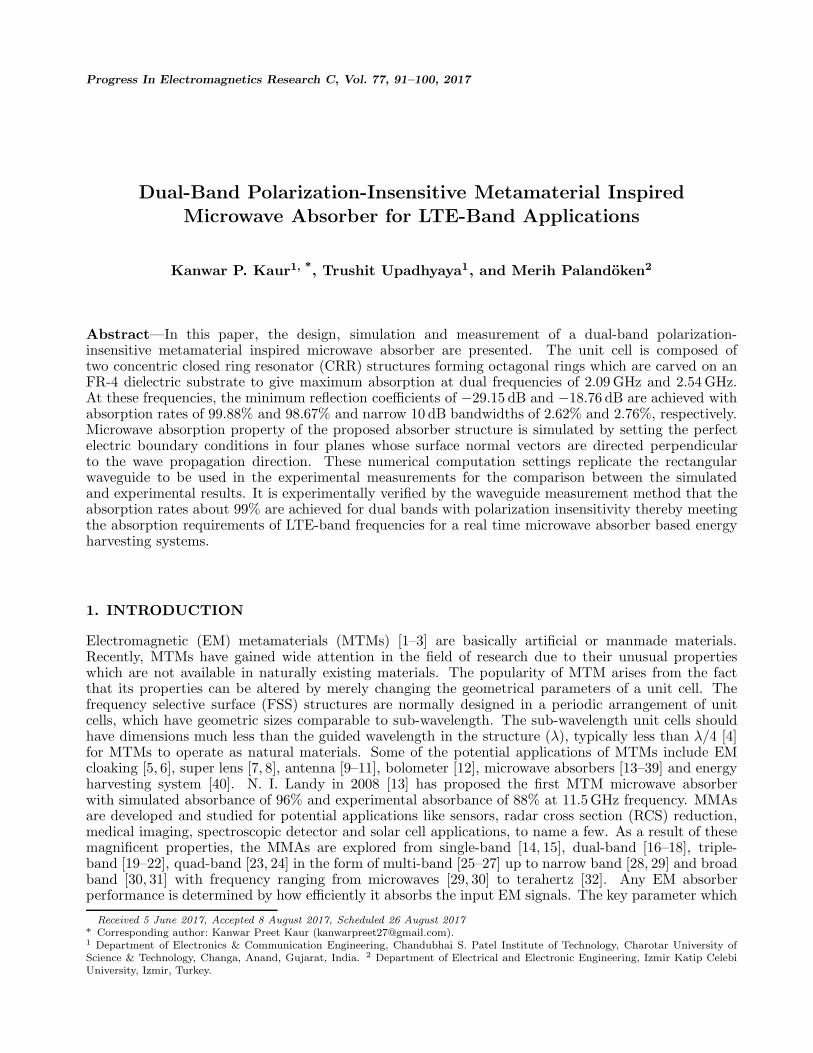
The proposed MMA design with its optimized geometrical dimensions is shown in Fig. 1. The unitcell is made up of two concentric octagonal rings forming CRRs. Outer CRR results in the first lowerfrequency absorption maxima whereas inner CRR gives rise to the second higher frequency absorption
Progress In Electromagnetics Research C, Vol. 77, 2017 93
Figure 1. Proposed absorber structure geometries with concentric octagonal rings: Front view of anoptimized sample and a single unit cell.
(a) (b)
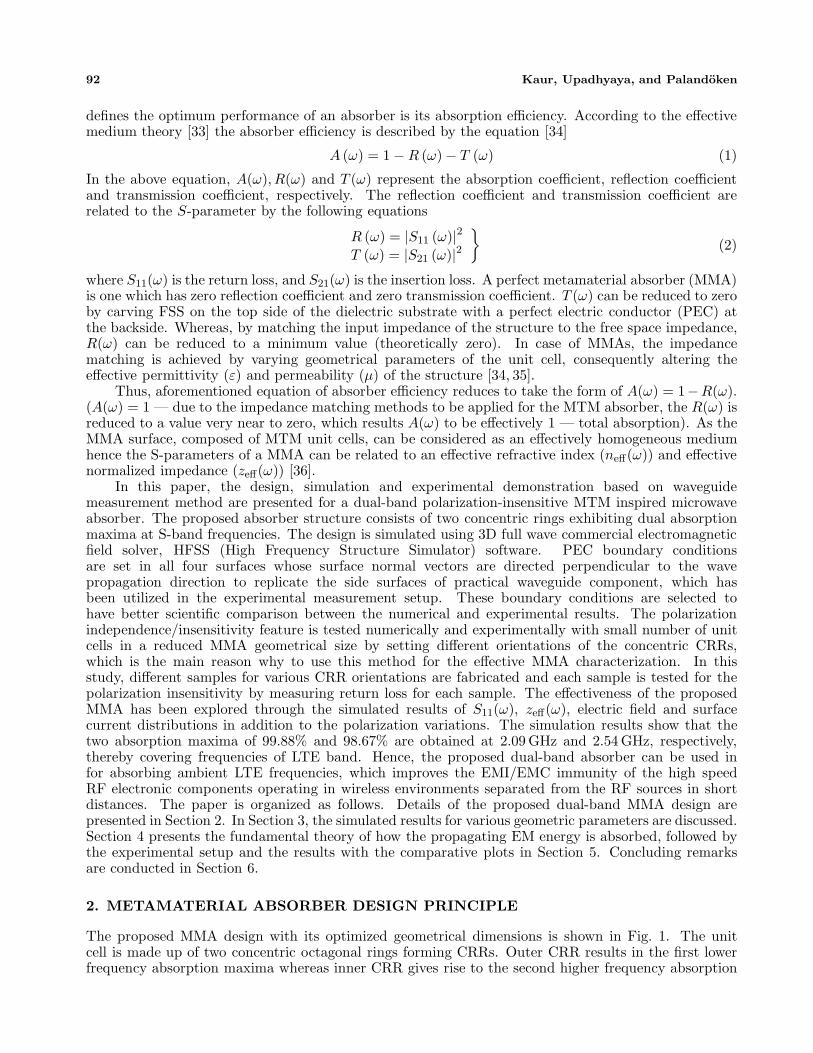
Figure 2. Simulated results of proposed absorber structure under normal incidence: (a) ReflectionCoefficient, S11(ω) and (b) Absorption, A(ω).
peak. These concentric CRRs are engraved on a double-sided metalized FR-4 dielectric substrate of2.4 mm thickness. The copper layer has the conductivity of 5.8×10⁷ S/m and thickness of 0.035 mm. Therelative permittivity of FR4 is 4.4 with the dielectric loss tangent of 0.02. The optimized geometricaldimensions of the proposed structure are as follows: a = 27.4 mm, R1 = 13.4 mm, R2 = 12.52 mm,w1 = 0.44 mm and w2 = 2.8 mm. The final MMA has the thickness of approximately λ/58 and maximumlateral size less than λ/5 at low frequency resonance.
3. NUMERICAL COMPUTATION RESULTS
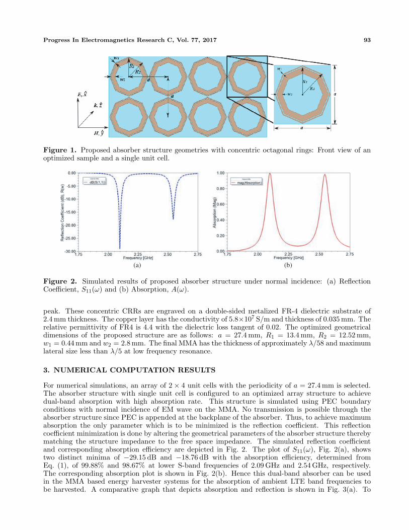
For numerical simulations, an array of 2 × 4 unit cells with the periodicity of a = 27.4 mm is selected.The absorber structure with single unit cell is configured to an optimized array structure to achievedual-band absorption with high absorption rate. This structure is simulated using PEC boundaryconditions with normal incidence of EM wave on the MMA. No transmission is possible through theabsorber structure since PEC is appended at the backplane of the absorber. Thus, to achieve maximumabsorption the only parameter which is to be minimized is the reflection coefficient. This reflectioncoefficient minimization is done by altering the geometrical parameters of the absorber structure therebymatching the structure impedance to the free space impedance. The simulated reflection coefficientand corresponding absorption efficiency are depicted in Fig. 2. The plot of S11(ω), Fig. 2(a), showstwo distinct minima of −29.15 dB and −18.76 dB with the absorption efficiency, determined fromEq. (1), of 99.88% and 98.67% at lower S-band frequencies of 2.09 GHz and 2.54 GHz, respectively.The corresponding absorption plot is shown in Fig. 2(b). Hence this dual-band absorber can be usedin the MMA based energy harvester systems for the absorption of ambient LTE band frequencies tobe harvested. A comparative graph that depicts absorption and reflection is shown in Fig. 3(a). To
94 Kaur, Upadhyaya, and Palandoken
achieve the desired condition of impedance matching the structure is optimized such that the impedanceof the MMA structure roughly matches to the free space impedance where the real component ofnormalized zeff (ω) is nearly equal to unity whereas imaginary component approaches to zero. Theretrieved impedance, illustrated in Fig. 3(b), shows that the two impedances roughly match at thefrequencies where z′eff (ω) ≈ 1 (real component) and z′′eff (ω) ≈ 0 (imaginary component).
(a) (b)
Figure 3. (a) Comparative graphs depicting absorption, A(ω) and reflection, R(ω) and (b) effectivenormalized impedance, zeff(ω).
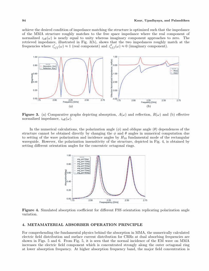
In the numerical calculations, the polarization angle (φ) and oblique angle (θ) dependences of thestructure cannot be obtained directly by changing the φ and θ angles in numerical computation dueto setting of the wave polarization and incidence angles by H10 fundamental mode of the rectangularwaveguide. However, the polarization insensitivity of the structure, depicted in Fig. 4, is obtained bysetting different orientation angles for the concentric octagonal rings.
Figure 4. Simulated absorption coefficient for different FSS orientation replicating polarization anglevariation.
4. METAMATERIAL ABSORBER OPERATION PRINCIPLE
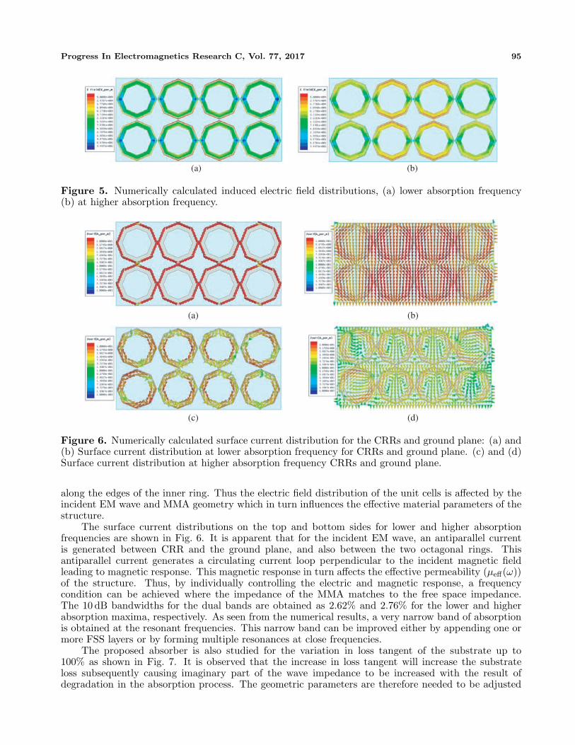
For comprehending the fundamental physics behind the absorption in MMA, the numerically calculatedelectric field distribution and surface current distribution for CRRs at dual absorbing frequencies areshown in Figs. 5 and 6. From Fig. 5, it is seen that the normal incidence of the EM wave on MMAincreases the electric field component which is concentrated strongly along the outer octagonal ringat lower absorption frequency. At higher absorption frequency band, the major field concentration is
Progress In Electromagnetics Research C, Vol. 77, 2017 95
(a) (b)
Figure 5. Numerically calculated induced electric field distributions, (a) lower absorption frequency(b) at higher absorption frequency.
(a) (b)
(c) (d)
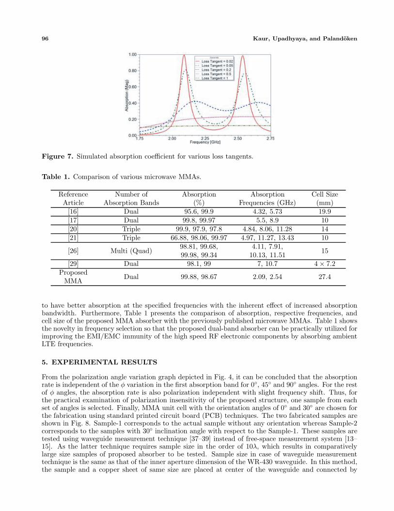
Figure 6. Numerically calculated surface current distribution for the CRRs and ground plane: (a) and(b) Surface current distribution at lower absorption frequency for CRRs and ground plane. (c) and (d)Surface current distribution at higher absorption frequency CRRs and ground plane.
along the edges of the inner ring. Thus the electric field distribution of the unit cells is affected by theincident EM wave and MMA geometry which in turn influences the effective material parameters of thestructure.
The surface current distributions on the top and bottom sides for lower and higher absorptionfrequencies are shown in Fig. 6. It is apparent that for the incident EM wave, an antiparallel currentis generated between CRR and the ground plane, and also between the two octagonal rings. Thisantiparallel current generates a circulating current loop perpendicular to the incident magnetic fieldleading to magnetic response. This magnetic response in turn affects the effective permeability (μeff(ω))of the structure. Thus, by individually controlling the electric and magnetic response, a frequencycondition can be achieved where the impedance of the MMA matches to the free space impedance.The 10 dB bandwidths for the dual bands are obtained as 2.62% and 2.76% for the lower and higherabsorption maxima, respectively. As seen from the numerical results, a very narrow band of absorptionis obtained at the resonant frequencies. This narrow band can be improved either by appending one ormore FSS layers or by forming multiple resonances at close frequencies.
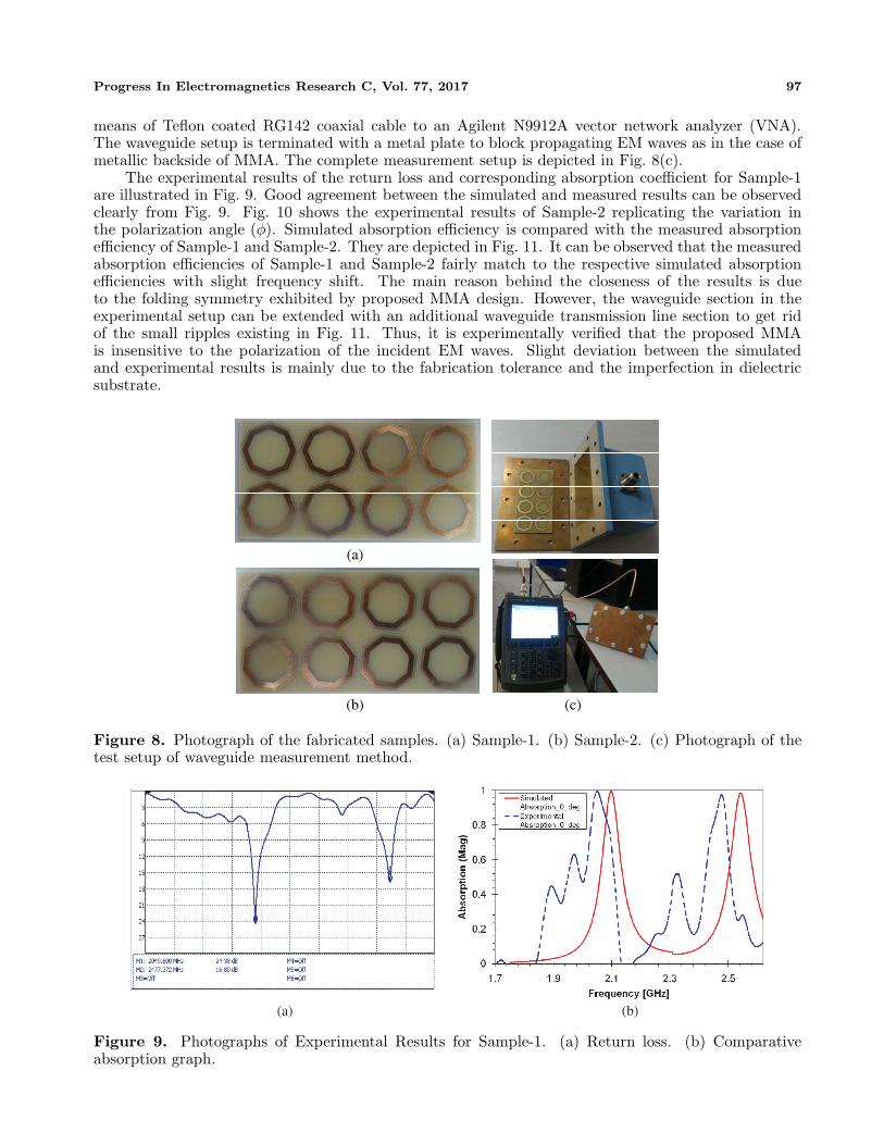
The proposed absorber is also studied for the variation in loss tangent of the substrate up to100% as shown in Fig. 7. It is observed that the increase in loss tangent will increase the substrateloss subsequently causing imaginary part of the wave impedance to be increased with the result ofdegradation in the absorption process. The geometric parameters are therefore needed to be adjusted
96 Kaur, Upadhyaya, and Palandoken
Figure 7. Simulated absorption coefficient for various loss tangents.
Table 1. Comparison of various microwave MMAs.
ReferenceArticle
Number ofAbsorption Bands
Absorption(%)
AbsorptionFrequencies (GHz)
Cell Size(mm)
[16] Dual 95.6, 99.9 4.32, 5.73 19.9[17] Dual 99.8, 99.97 5.5, 8.9 10[20] Triple 99.9, 97.9, 97.8 4.84, 8.06, 11.28 14[21] Triple 66.88, 98.06, 99.97 4.97, 11.27, 13.43 10
[26] Multi (Quad)98.81, 99.68,99.98, 99.34
4.11, 7.91,10.13, 11.51 15
[29] Dual 98.1, 99 7, 10.7 4 × 7.2Proposed
MMA Dual 99.88, 98.67 2.09, 2.54 27.4
to have better absorption at the specified frequencies with the inherent effect of increased absorptionbandwidth. Furthermore, Table 1 presents the comparison of absorption, respective frequencies, andcell size of the proposed MMA absorber with the previously published microwave MMAs. Table 1 showsthe novelty in frequency selection so that the proposed dual-band absorber can be practically utilized forimproving the EMI/EMC immunity of the high speed RF electronic components by absorbing ambientLTE frequencies.
5. EXPERIMENTAL RESULTS
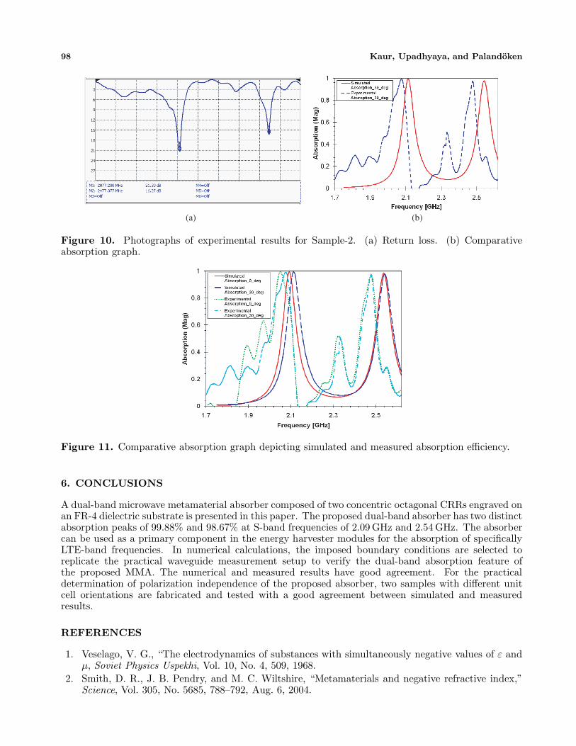
From the polarization angle variation graph depicted in Fig. 4, it can be concluded that the absorptionrate is independent of the φ variation in the first absorption band for 0◦, 45◦ and 90◦ angles. For the restof φ angles, the absorption rate is also polarization independent with slight frequency shift. Thus, forthe practical examination of polarization insensitivity of the proposed structure, one sample from eachset of angles is selected. Finally, MMA unit cell with the orientation angles of 0◦ and 30◦ are chosen forthe fabrication using standard printed circuit board (PCB) techniques. The two fabricated samples areshown in Fig. 8. Sample-1 corresponds to the actual sample without any orientation whereas Sample-2corresponds to the samples with 30◦ inclination angle with respect to the Sample-1. These samples aretested using waveguide measurement technique [37–39] instead of free-space measurement system [13–15]. As the latter technique requires sample size in the order of 10λ, which results in comparativelylarge size samples of proposed absorber to be tested. Sample size in case of waveguide measurementtechnique is the same as that of the inner aperture dimension of the WR-430 waveguide. In this method,the sample and a copper sheet of same size are placed at center of the waveguide and connected by
Progress In Electromagnetics Research C, Vol. 77, 2017 97
means of Teflon coated RG142 coaxial cable to an Agilent N9912A vector network analyzer (VNA).The waveguide setup is terminated with a metal plate to block propagating EM waves as in the case ofmetallic backside of MMA. The complete measurement setup is depicted in Fig. 8(c).
The experimental results of the return loss and corresponding absorption coefficient for Sample-1are illustrated in Fig. 9. Good agreement between the simulated and measured results can be observedclearly from Fig. 9. Fig. 10 shows the experimental results of Sample-2 replicating the variation inthe polarization angle (φ). Simulated absorption efficiency is compared with the measured absorptionefficiency of Sample-1 and Sample-2. They are depicted in Fig. 11. It can be observed that the measuredabsorption efficiencies of Sample-1 and Sample-2 fairly match to the respective simulated absorptionefficiencies with slight frequency shift. The main reason behind the closeness of the results is dueto the folding symmetry exhibited by proposed MMA design. However, the waveguide section in theexperimental setup can be extended with an additional waveguide transmission line section to get ridof the small ripples existing in Fig. 11. Thus, it is experimentally verified that the proposed MMAis insensitive to the polarization of the incident EM waves. Slight deviation between the simulatedand experimental results is mainly due to the fabrication tolerance and the imperfection in dielectricsubstrate.
(a)
(b) (c)
Figure 8. Photograph of the fabricated samples. (a) Sample-1. (b) Sample-2. (c) Photograph of thetest setup of waveguide measurement method.
(a) (b)
Figure 9. Photographs of Experimental Results for Sample-1. (a) Return loss. (b) Comparativeabsorption graph.
98 Kaur, Upadhyaya, and Palandoken
(a) (b)
Figure 10. Photographs of experimental results for Sample-2. (a) Return loss. (b) Comparativeabsorption graph.
Figure 11. Comparative absorption graph depicting simulated and measured absorption efficiency.
6. CONCLUSIONS
A dual-band microwave metamaterial absorber composed of two concentric octagonal CRRs engraved onan FR-4 dielectric substrate is presented in this paper. The proposed dual-band absorber has two distinctabsorption peaks of 99.88% and 98.67% at S-band frequencies of 2.09 GHz and 2.54 GHz. The absorbercan be used as a primary component in the energy harvester modules for the absorption of specificallyLTE-band frequencies. In numerical calculations, the imposed boundary conditions are selected toreplicate the practical waveguide measurement setup to verify the dual-band absorption feature ofthe proposed MMA. The numerical and measured results have good agreement. For the practicaldetermination of polarization independence of the proposed absorber, two samples with different unitcell orientations are fabricated and tested with a good agreement between simulated and measuredresults.
REFERENCES
1. Veselago, V. G., “The electrodynamics of substances with simultaneously negative values of ε andμ, Soviet Physics Uspekhi, Vol. 10, No. 4, 509, 1968.
2. Smith, D. R., J. B. Pendry, and M. C. Wiltshire, “Metamaterials and negative refractive index,”Science, Vol. 305, No. 5685, 788–792, Aug. 6, 2004.
Progress In Electromagnetics Research C, Vol. 77, 2017 99
3. Smith, D. R., W. J. Padilla, D. C. Vier, S. C. Nemat-Nasser, and S. Schultz, “Composite mediumwith simultaneously negative permeability and permittivity,” Physical Review Letters, Vol. 84,No. 18, 4184, May 1, 2000.
4. Caloz, C. and T. Itoh, Electromagnetic Metamaterials: Transmission Line Theory and MicrowaveApplications, John Wiley & Sons, Nov. 2005, 22.
5. Schurig, D., J. J. Mock, B. J. Justice, S. A. Cummer, J. B. Pendry, A. F. Starr, and D. R. Smith,“Metamaterial electromagnetic cloak at microwave frequencies,” Science, Vol. 314, No. 5801, 977–980, Nov. 10, 2006.
6. Cai, W., U. K. Chettiar, A. V. Kildishev, and V. M. Shalaev, “Optical cloaking withmetamaterials,” Nature Photonics, Vol. 1, No. 4, 224–227, Apr. 1, 2007.
7. Pendry, J. B., “Negative refraction makes a perfect lens,” Physical Review Letters, Vol. 85, No. 18,3966, Oct. 30, 2000.
8. Fang, N. and X. Zhang, “Imaging properties of a metamaterial superlens,” Applied Physics Letters,Vol. 82, No. 2, 161–163, Jan. 13, 2003.
9. Upadhyaya, T. K., S. P. Kosta, R. Jyoti, and M. Palandoken, “Novel stacked μ-negative material-loaded antenna for satellite applications,” International Journal of Microwave and WirelessTechnologies, Vol. 8, No. 02, 229–235, Mar. 1, 2016.
10. Upadhyaya, T. K., S. P. Kosta, R. Jyoti, and M. Palandoken, “Negative refractive index material-inspired 90-deg electrically tilted ultra-wideband resonator,” Optical Engineering, Vol. 53, No. 10,107104, Oct. 1, 2014.
11. Palandoken, M., Artificial Materials Based Microstrip Antenna Design, INTECH Open AccessPublisher, 2011.
12. Niesler, F. B., J. K. Gansel, S. Fischbach, and M. Wegener, “Metamaterial metal-basedbolometers,” Applied Physics Letters, Vol. 100, No. 20, 203508, May 14, 2012.
13. Landy, N. I., S. Sajuyigbe, J. J. Mock, D. R. Smith, and W. J. Padilla, “Perfect metamaterialabsorber,” Physical Review Letters, Vol. 100, No. 20, 207402, May 21, 2008.
14. Zhu, B., Z. Wang, C. Huang, Y. Feng, J. Zhao, and T. Jiang, “Polarization insensitive metamaterialabsorber with wide incident angle,” Progress In Electromagnetics Research, Vol. 101, 231–239, 2010.
15. Cheng, Y. and H. Yang, “Design, simulation, and measurement of metamaterial absorber,” Journalof Applied Physics, Vol. 108, No. 3, 034906, Aug. 1, 2010.
16. Dincer, F., M. Karaaslan, E. Unal, K. Delihacioglu, and C. Sabah, “Design of polarization andincident angle insensitive dual-band metamaterial absorber based on isotropic resonators, ProgressIn Electromagnetics Research, Vol. 144, 123–132, 2014.
17. Ramya, S. and I. Srinivasa Rao, “Design of polarization-insensitive dual band metamaterialabsorber,” Progress In Electromagnetics Research M, Vol. 50, 23–31, 2016.
18. He, X. J., Y. Wang, J. Wang, T. Gui, and Q. Wu, “Dual-band terahertz metamaterial absorberwith polarization insensitivity and wide incident angle,” Progress In Electromagnetics Research,Vol. 115, 381-397, 2011.
19. Shen, X., Y. Yang, Y. Zang, J. Gu, J. Han, W. Zhang, and T. J. Cui, “Triple-band terahertzmetamaterial absorber: Design, experiment, and physical interpretation,” Applied Physics Letters,Vol. 101 No. 15, 154102, Oct. 8, 2012.
20. Wang, G. D., J. F. Chen, X. Hu, Z. Q. Chen, and M. Liu, “Polarization-insensitive triple-bandmicrowave metamaterial absorber based on rotated square rings,” Progress In ElectromagneticsResearch, Vol. 145, 175–183, 2014.
21. Sood, D., “A triple band ultra-thin metamaterial absorber with wide incident angle stability,”Indian Journal of Radio & Space Physics (IJRSP), Vol. 45, No. 2, 57–66, Dec. 29, 2016.
22. Yahiaoui, R., J. P. Guillet, F. de Miollis, and P. Mounaix, “Ultra-flexible multiband terahertzmetamaterial absorber for conformal geometry applications,” Optics Letters, Vol. 38, No. 23, 4988–4990, 2013.
23. Agarwal, M., A. K. Behera, and M. K. Meshram, “Wide-angle quad-band polarization-insensitivemetamaterial absorber,” Electronics Letters, Vol. 52, No. 5, 340–342, Jan. 22, 2016.
100 Kaur, Upadhyaya, and Palandoken
24. Wang, N., J. Tong, W. Zhou, W. Jiang, J. Li, X. Dong, and S. Hu, “Novel quadruple-bandmicrowave metamaterial absorber,” IEEE Photonics Journal, Vol. 7, No. 1, 1–6, Feb. 2015.
25. Park, J. W., P. V. Tuong, J. Y. Rhee, K. W. Kim, W. H. Jang, E. H. Choi, L. Y. Chen, and Y. Lee,“Multi-band metamaterial absorber based on the arrangement of donut-type resonators,” OpticsExpress, Vol. 21, No. 8, 9691–9702, Apr. 22, 2013.
26. Chaurasiya, D., S. Ghosh, S. Bhattacharyya, A. Bhattacharya, and K. V. Srivastava,“Compact multi-band polarization-insensitive metamaterial absorber,” IET Microwaves, Antennas& Propagation, Vol. 10, No. 1, 94–101, Jan. 9, 2016.
27. Yahiaoui, R., S. Tan, L. Cong, R. Singh, F. Yan, and W. Zhang, “Multispectral terahertz sensingwith highly flexible ultrathin metamaterial absorber,” Journal of Applied Physics, Vol. 118, No. 8,083103, 2015.
28. Huang, Y. J., G. J. Wen, J. Li, W. R. Zhu, P. Wang, and Y. H. Sun, “Wide-angle andpolarization-independent metamaterial absorber based on snowflake-shaped configuration,” Journalof Electromagnetic Waves and Applications, Vol. 27, No. 5, 552–559, Mar. 1, 2013.
29. Ramya, S. and I. Srinivasa Rao, “Dual band microwave metamaterial absorber using loop resonatorfor electromagnetic interference suppression,” Int. J. Appl. Eng. Res., Vol. 10, No. 30, 22712-22715,2015.
30. Ding, F., Y. Cui, X. Ge, Y. Jin, and S. He, “Ultra-broadband microwave metamaterial absorber,”Applied Physics Letters, Vol. 100, No. 10, 103506, Mar. 5, 2012.
31. Liu, Y., S. Gu, C. Luo, and X. Zhao, “Ultra-thin broadband metamaterial absorber,” AppliedPhysics A, Vol. 108, No. 1, 19–24, Jul. 1, 2012.
32. Yahiaoui, R., K. Hanai, K. Takano, T. Nishida, F. Miyamaru, M. Nakajima, and M. Hangyo,“Trapping waves with terahertz metamaterial absorber based on isotropic Mie resonators,” OpticsLetters, Vol. 40, No. 13, 3197–3200, 2015.
33. Liu, R., T. J. Cui, D. Huang, B. Zhao, and D. R. Smith, “Description and explanation ofelectromagnetic behaviors in artificial metamaterials based on effective medium theory,” PhysicalReview E, Vol. 76, No. 2, 026606, Aug. 23, 2007.
34. Tao, H., N. I. Landy, C. M. Bingham, X. Zhang, R. D. Averitt, and W. J. Padilla, “A metamaterialabsorber for the terahertz regime: Design, fabrication and characterization,” Optics Express,Vol. 16, No. 10, 7181–7188, May 12, 2008.
35. Tao, H., C. M. Bingham, A. C. Strikwerda, D. Pilon, D. Shrekenhamer, N. I. Landy, K. Fan,X. Zhang, W. J. Padilla, and R. D. Averitt, “Highly flexible wide angle of incidence terahertzmetamaterial absorber: Design, fabrication, and characterization,” Physical Review B, Vol. 78,No. 24, 241103, Dec. 19, 2008.
36. Smith, D. R., D. C. Vier, T. Koschny, and C. M. Soukoulis, “Electromagnetic parameter retrievalfrom inhomogeneous metamaterials,” Physical Review E, Mar. 22, 2005, Vol. 71, No. 3, 036617.
37. Li, L., Y. Yang, and C. Liang, “A wide-angle polarization-insensitive ultra-thin metamaterialabsorber with three resonant modes,” Journal of Applied Physics, Sep. 15, 2011, Vol. 110, No. 6,063702.
38. Lu, L., S. Qu, H. Ma, F. Yu, S. Xia, Z. Xu, and P. Bai, “A polarization-independent wide-angle dualdirectional absorption metamaterial absorber,” Progress In Electromagnetics Research M, Vol. 27,91–201, 2012.
39. Zhai, H., C. Zhan, L. Liu, and Y. Zang, “Reconfigurable wideband metamaterial absorber withwide angle and polarisation stability,” Electronics Letters, Vol. 51, No. 21, 1624–1626, Oct. 1, 2015.
40. Palandoken, M., “Microstrip antenna with compact anti-spiral slot resonator for 2.4 GHz energyharvesting applications,” Microwave and Optical Technology Letters, Vol. 58, No. 6, 1404–1408,2016.