e-nano newsletter nº 2
DESCRIPTION
Welcome to the second issue of the E-NANO Newsletter that threemonthly provides the latest news, research articles, reports and resources from the Nanotechnology world. Creating an Atomic Scale Technology is now a necessity for any uni-molecular device and machine in molecular electronics, molecular mechanics, molecular transducers and for laboratory scale experiments on one molecule. In the IST priority 2 of Framework Programme 6 (Emerging Nanoelectronics FET proactive initiative), the Pico-Inside consortium will explore Atomic Scale Technology with the final goal of integrating a complex logic gate inside a single molecule.TRANSCRIPT
Charge Transport in DNA
newsletteroctober 2005
http://www.phantomsnet.net
Enº 2
CNTs Attached to AFM Microcantilevers and STM Tips
Hybrid and Mono Molecular Electronics

www.phantomsnet.net E newsletter October 2005 3
Contents
newsletter
EEditorial Information 4
ResearchCharge Transport in DNA 5S. Roche, F. Triozon and E. Maciá
HighlightBiotechnical Microsystems Dept. of IPHT Jena (Germany) 9
Pico-Inside Integrated Project
Hybrid and Mono Molecular Electronics 12Background before starting the PICO-INSIDE IST FET European Integrated Project
C. Joachim
Pico-Inside: Summary, Objetives and Partners 17Groups involved in the IST-FET Integrated project
NANO News 21
NANO Conferences 23
NANO Vacancies 24
ResearchCNTs Attached to AFM Microcantilevers and STM Tips 25A. Raman and R. Reifenberger
4 E newsletter October 2005 www.phantomsnet.net
Cover Picture:Interconnecting a molecular wire sup-ported by 4 legs to a mono-atomicstep edge on Cu(111). LT UHV-STMimage of the molecule at contact.(Ref: F. Moresco et al., Phys. Rev.Lett., 91, 036601 (2003))Pico-Inside logo courtesy:MIDAM Production sprl18, rue du Verger1950 Kraainem Belgique
EDITORIALINFORMATION
E newsletter nº2October 2005Published byPHANTOMS Foundation (Spain)
Editor:Dr. Antonio CorreiaPHANTOMS [email protected]
Associated Editor:Fernando HernándezPHANTOMS [email protected]
Editorial Board:Ron Reifenberger (Purdue University,USA) Stephan Roche (CEA-DRFMC,France)Juan Jose Saenz (UAM, Spain)Pedro A. Serena (ICMM-CSIC, Spain) Rainer Waser (Research CenterJulich, Germany)
For any question please contact theeditor at:[email protected]: +34 91 4973471
1000 copies of this issue have beenprinted.
Subscription rates (shipping included)are (Euro/year):-Europe: 100 Euros-Non-European Countries: 150 Euros
Advertising:We welcome sponsors and adverti-sers.Please visit http://www.phantoms-net.net/Foundation/advertising.php todownload our media data and adver-tising rates
Advertisers:www.nanobuildings.com (p.2),NanoMEGAS (p.16), Nanotec (p.27), Raith (p.31), Scientec (p. 31),Orsay Physics (p. 32)
PHANTOMS FoundationParque Científico de MadridPabellón CCampus de Cantoblanco - UAMCtra de Colmenar km 1528049 Madrid (Spain)FAX: +34 91 4973471
Web: www.phantomsnet.net
Editorial
Dear Readers:
Welcome to the second issue of theE-NANO Newsletter that three-monthly provides the latest news,research articles, reports and resour-ces from the Nanotechnology world.
Creating an Atomic Scale Technologyis now a necessity for any uni-mole-cular device and machine in molecu-lar electronics, molecular mechanics,molecular transducers and for labora-tory scale experiments on one mole-cule. In the IST priority 2 ofFramework Programme 6 (EmergingNanoelectronics FET proactive initia-tive), the Pico-Inside consortium willexplore Atomic Scale Technology withthe final goal of integrating a complexlogic gate inside a single molecule.The E-NANO newsletter will three-monthly publish relevant informationand latest results about the Pico-Inside (IST/FET/NANO) project, rai-sing therefore awareness of scientistsin this emerging research area. In this issue, we publish a review arti-cle prepared by Prof. ChristianJoachim (CEMES/CNRS - GNS,France) on the current status of"Molecular Electronics" and a list ofthe partners involved in the IntegratedProject, detailing their activities andcore competences.
In addition, two research articles pro-vide insights in “Charge Transport inDNA” and “CNTs attached to AFMMicrocantilevers and STM Tips”.These two studies are particularlyimportant due respectively to theirpossible applications in future(bio)electronics or DNA-based chipsand in Scanning Probe Microscopy.
We invite readers to send us theirscientific contributions either as arti-cles, reviews or publication highlights.
We would like to thanks all theauthors who contributed to this issueas well as the European Commission(IST/FET/NANO) for its close collabo-ration.
Dr. Antonio Correia (Editor)Phantoms Foundation
Deadline for manuscriptsubmission:
Issue nº03: December 15, 2005Issue nº04: March 15, 2006
Depósito Legal: M-43078-2005

Charge Transport in DNA
S. Roche* 1, F. Triozon 1 and E. Macià 2
1 CEA/DSM/DRFMC/SPSMS, Grenoble (France)2 Dpto. de Física de Materiales, Fac. CC. Físicas, UCM
(Spain) *Corresponding Author: [email protected]
Abstract: The Charge transport in desoxyribonucleic acid (DNA)is being intensively investigated in view of its biological implica-tions in damage and repair, protein bonding, and envisioned inte-gration in future (bio)electronics or DNA-based chips.Notwithstanding, despite sustained efforts to unveil the natureand range of charge transfer in these biomolecules, presentknowledge lacks stable foundations. Here we discuss basics ofcharge transport in the quantum coherent regime (unistep tun-neling), and shows that some concepts of electronic conductionneed to be revisited for DNA.
Keywords: DNA, charge transport, nanoelectronics, coherenttunnelling.
1. Introduction
The double-helix structure of DNA is made from two weak-ly hydrogen-bonded strands, each of which, consisting ina sequence of four nucleotides (A-adenine, T-thymine, C-cytosine, G-guanine) that strictly follows the Watson-Crickcomplementarities law (i.e. interstrand pairs only appearas AT or CG). Charge transport is believed to be conveyedthrough the highest occupied molecular orbitals of theguanine base (G-HOMO), given its smaller ionizationpotential.
In the recent years, two kinds of experiments have provid-ed valuable information on charge transfer in DNA. First,fluorescence experiments have relied on the use of inter-calated metallic complexes acting as donor and acceptorto photoinduce and follow charge migration along smallDNA fragments [1,2]. Such experiments have pointedtowards an efficient transfer over unprecedented lengthscale for biomolecules. Other experiments have focusedon contacting DNA with conducting electrodes, and per-forming mesoscopic conductance measurements undervarious physical conditions. Presently available resultslack consistency since all kinds of transport regimes havebeen proposed, from metallic-like, superconducting, semi-conducting or strongly insulating behaviours. Transportmechanism might be purely hole transport, or polaronic-based.
2. Theoretical model for charge transfer
We have recently performed a theoretical study on sever-al kinds of both artificial or genomic DNA. To discuss basictransport mechanisms we have elaborated on a modellingof hole transport through the guanine bases, describedwithin an effective 1D tight binding Hamiltonian,
Η = Σn − tDNA cos(θn,n+1)(cn†cn+1 + h.c.) + εncn
†cn
cn† (cn) is the operator corresponding to charge creation
(annihilation) at site n, tDNA gives the amplitude of π−πcoupling between nearest neighbours orbitals, εn the holesite energies and cos(θn,n+1) is temperature dependentand describes the lowering of coupling between basepairs due to thermal fluctuations [3].
In order to evaluate the conductivity of the system, we usethe Landauer formulation of electron transmission, and wecompute the energy-dependent transmission coefficientT(E). Our modelling is such that the full energy dependenceof T is necessary to discuss the charge transfer properties,although the DNA chain is connected to metallic leads andthe electrode Fermi levels are lined up to the G-HOMO. Inthe Landauer formalism used here, one considers an elec-tronic wavepacket of wave vector k and energy E which isinjected from a metallic contact (see Fig.1) inside a DNAsequence. The coefficients R and T give the amplitudeswhich are respectively reflected by the DNA sequence andtransmitted to another one or to the other metallic contact.Current conservation implies R+T=1. The inverse transmis-sion rate R/T is related to the dimensionless resistance (ρ),and for weak transmission, the DNA resistivity is proportion-al to [(1-Tav)/Tav] SDNA/LDNA taking Tav an average of thetransmission coefficient for energies close to the HOMO-Gionisation energy, SDNA=3.10
-18m2 the average DNA cross
section, and LDNA the sequence length [3].
3. Charge transfer in periodic PolyG-PolyC sequences
We have considered synthetic Poly(dG)-Poly(dC)sequences consisting of G and C bases alternated on eachstrand and sequences extracted from the biological λ-bac-teriophage or from the Human Chromosome 22 DNA. Thetransmission coefficient was studied for finite sequencefrom 20 nm up to 200 nm long.
As expected Poly(dG)-Poly(dC) sequences were found tofollow a “semiconducting-like” regime mainly due to a trans-mission gap stemming from the two spectral bands (seeFig. 1). The transmission is equal to one at resonant states,whose number is proportional to the number of nucleotideinside the DNA sequence. The bandwidth of the transmis-sion bands is proportional to the parameter tDNA , which ishere taken as tDNA =0.4, to reproduce ab-initio results.
www.phantomsnet.net E newsletter October 2005 5
Figure1: Representation of the transmission throughout a DNAsequence connected to two metallic contacts.
Research
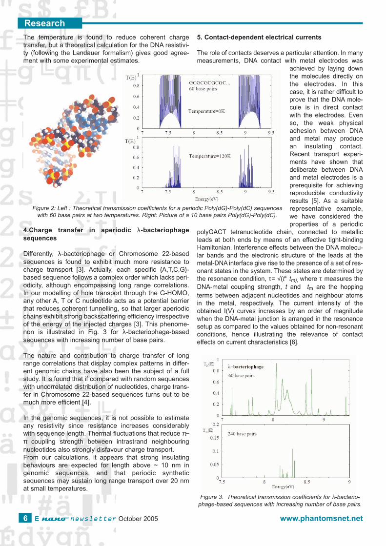
The temperature is found to reduce coherent chargetransfer, but a theoretical calculation for the DNA resistivi-ty (following the Landauer formalism) gives good agree-ment with some experimental estimates.
4.Charge transfer in aperiodic λ-bacteriophagesequences
Differently, λ-bacteriophage or Chromosome 22-basedsequences is found to exhibit much more resistance tocharge transport [3]. Actually, each specific {A,T,C,G}-based sequence follows a complex order which lacks peri-odicity, although encompassing long range correlations.In our modelling of hole transport through the G-HOMO,any other A, T or C nucleotide acts as a potential barrierthat reduces coherent tunnelling, so that larger aperiodicchains exhibit strong backscattering efficiency irrespectiveof the energy of the injected charges [3]. This phenome-non is illustrated in Fig. 3 for λ-bacteriophage-basedsequences with increasing number of base pairs.
The nature and contribution to charge transfer of longrange correlations that display complex patterns in differ-ent genomic chains have also been the subject of a fullstudy. It is found that if compared with random sequenceswith uncorrelated distribution of nucleotides, charge trans-fer in Chromosome 22-based sequences turns out to bemuch more efficient [4].
In the genomic sequences, it is not possible to estimateany resistivity since resistance increases considerablywith sequence length. Thermal fluctuations that reduce π−π coupling strength between intrastrand neighbouringnucleotides also strongly disfavour charge transport. From our calculations, it appears that strong insulatingbehaviours are expected for length above ~ 10 nm ingenomic sequences, and that periodic syntheticsequences may sustain long range transport over 20 nmat small temperatures.
5. Contact-dependent electrical currents
The role of contacts deserves a particular attention. In manymeasurements, DNA contact with metal electrodes was
achieved by laying downthe molecules directly onthe electrodes. In thiscase, it is rather difficult toprove that the DNA mole-cule is in direct contactwith the electrodes. Evenso, the weak physicaladhesion between DNAand metal may producean insulating contact.Recent transport experi-ments have shown thatdeliberate between DNAand metal electrodes is aprerequisite for achievingreproducible conductivityresults [5]. As a suitablerepresentative example,we have considered theproperties of a periodic
polyGACT tetranucleotide chain, connected to metallicleads at both ends by means of an effective tight-bindingHamiltonian. Interference effects between the DNA molecu-lar bands and the electronic structure of the leads at themetal-DNA interface give rise to the presence of a set of res-onant states in the system. These states are determined bythe resonance condition, τ= √(t* tm), where τ measures theDNA-metal coupling strength, t and tm are the hoppingterms between adjacent nucleotides and neighbour atomsin the metal, respectively. The current intensity of theobtained I(V) curves increases by an order of magnitudewhen the DNA-metal junction is arranged in the resonancesetup as compared to the values obtained for non-resonantconditions, hence illustrating the relevance of contacteffects on current characteristics [6].
Figure 2: Left : Theoretical transmission coefficients for a periodic Poly(dG)-Poly(dC) sequenceswith 60 base pairs at two temperatures. Right: Picture of a 10 base pairs Poly(dG)-Poly(dC).
6 E newsletter October 2005 www.phantomsnet.net
Figure 3. Theoretical transmission coefficients for λ-bacterio-phage-based sequences with increasing number of base pairs.
Research
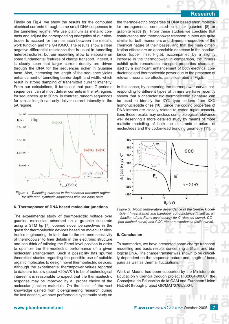
Finally on Fig.4, we show the results for the computedelectrical currents through some small DNA sequences inthe tunnelling regime. We use platinum as metallic con-tacts and adjust the corresponding energetics of our elec-trodes to account for the mismatch between the metallicwork function and the G-HOMO. The results show a clearnegative differential resistance that is usual in tunnellingheterostructures, but our modelling allow to elaborate onsome fundamental features of charge transport. Indeed, itis clearly seen that larger current density are driventhrough the DNA for the sequences richer in Guaninebase. Also, increasing the length of the sequence yieldsenhancement of tunnelling barrier depth and width, whichresult in strong damping of transmitted current intensity.From our calculations, it turns out that pure G-periodicsequences, can at most deliver currents in the nA regime,for sequences up to 20nm. In contrast, random sequencesfor similar length can only deliver current intensity in thepA regime.
6. Thermopower of DNA based molecular junctions
The experimental study of thermoelectric voltage overguanine molecules adsorbed on a graphite substrateusing a STM tip [7], opened novel perspectives in thequest for thermoelectric devices based on molecular elec-tronics engineering. In fact, due to the extreme sensitivityof thermopower to finer details in the electronic structureone can think of tailoring the Fermi level position in orderto optimize the thermoelectric performance of a givenmolecular arrangement. Such a possibility has spurredtheoretical studies regarding the possible use of suitableorganic molecules to design novel thermoelectric devices.Although the experimental thermopower values reportedto date are too low (about +20µVK-1) to be of technologicalinterest, it is reasonable to expect that the thermoelectricresponse may be improved by a proper choice of themolecular junction materials. On the basis of the vastknowledge gained from bioengineering research duringthe last decade, we have performed a systematic study on
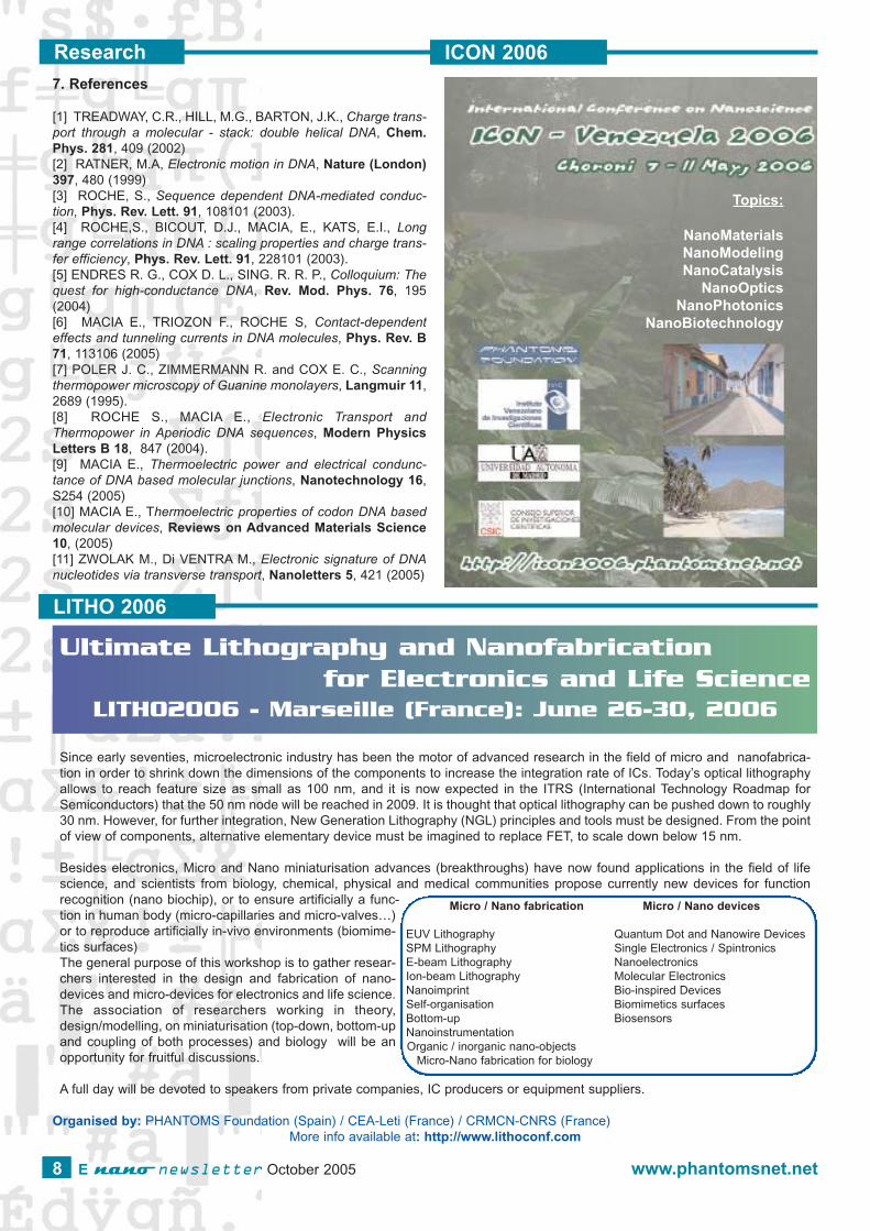
the thermoelectric properties of DNA based short molecu-lar arrangements connected to either guanine [8] orgraphite leads [9]. From these studies we conclude thatconductance and thermopower transport curves are quitesimilar for both monomers and dimers, irrespective of thechemical nature of their bases, and that the main dimer-ization effects are an appreciable decrease in the conduc-tance (upper inset Fig.5), accompanied by a slightlyincrease in the thermopower. In comparison, the trimersexhibit quite remarkable transport properties character-ized by a significant enhancement of both electrical con-ductance and thermoelectric power due to the presence ofrelevant resonance effects, as it illustrated in Fig.5.
In this sense, by comparing the thermopower curves cor-responding to different types of trimers we have recentlyshown that a characteristic thermoelectric signature canbe used to identify the XYX type codons from XXXhomonucleotide ones [10]. Since the coding properties ofDNA introns are closely related to codon triplet associa-tions these results may enclose some biological relevancewell deserving a more detailed study by means of morerealistic modelling of both the electronic structure ofnucleotides and the codon-lead bonding geometry [11].
6. Conclusion
To summarize, we have presented some charge transportmodelling and basic results concerning artificial and bio-logical DNA. The charge transfer was shown to be critical-ly dependent on the sequence nature and length of basepairs as well as thermal fluctuations.
Work at Madrid has been supported by the Ministerio deEducación y Ciencia through project FIS2004-00067, theConsejería de Educación de la CAM and European UnionFEDER through project GR/MAT/0768/2004.
Figure 4. Tunneling currents in the coherent transport regimefor different synthetic sequences with ten base pairs.
Figure 5. Room temperature dependence of the Seebeck coef-ficient (main frame) and Landauer condunctance (inset) as afunction of the Fermi level energy for C (dashed curve), CC
(dot-dashed curve) and CCC trimer nucleobases (solid curve).
www.phantomsnet.net E newsletter October 2005 7
Research
7. References
[1] TREADWAY, C.R., HILL, M.G., BARTON, J.K., Charge trans-port through a molecular - stack: double helical DNA, Chem.Phys. 281, 409 (2002)[2] RATNER, M.A, Electronic motion in DNA, Nature (London)397, 480 (1999)[3] ROCHE, S., Sequence dependent DNA-mediated conduc-tion, Phys. Rev. Lett. 91, 108101 (2003).[4] ROCHE,S., BICOUT, D.J., MACIA, E., KATS, E.I., Longrange correlations in DNA : scaling properties and charge trans-fer efficiency, Phys. Rev. Lett. 91, 228101 (2003).[5] ENDRES R. G., COX D. L., SING. R. R. P., Colloquium: Thequest for high-conductance DNA, Rev. Mod. Phys. 76, 195(2004)[6] MACIA E., TRIOZON F., ROCHE S, Contact-dependenteffects and tunneling currents in DNA molecules, Phys. Rev. B71, 113106 (2005) [7] POLER J. C., ZIMMERMANN R. and COX E. C., Scanningthermopower microscopy of Guanine monolayers, Langmuir 11,2689 (1995). [8] ROCHE S., MACIA E., Electronic Transport andThermopower in Aperiodic DNA sequences, Modern PhysicsLetters B 18, 847 (2004).[9] MACIA E., Thermoelectric power and electrical condunc-tance of DNA based molecular junctions, Nanotechnology 16,S254 (2005)[10] MACIA E., Thermoelectric properties of codon DNA basedmolecular devices, Reviews on Advanced Materials Science10, (2005)[11] ZWOLAK M., Di VENTRA M., Electronic signature of DNAnucleotides via transverse transport, Nanoletters 5, 421 (2005)
8 E newsletter October 2005 www.phantomsnet.net
Research
LITHO 2006
ICON 2006
Topics:
NanoMaterialsNanoModelingNanoCatalysis
NanoOpticsNanoPhotonics
NanoBiotechnology
Ultimate Lithography and Nanofabricationfor Electronics and Life Science
LITHO2006 - Marseille (France): June 26-30, 2006
Organised by: PHANTOMS Foundation (Spain) / CEA-Leti (France) / CRMCN-CNRS (France)More info available at: http://www.lithoconf.com
Since early seventies, microelectronic industry has been the motor of advanced research in the field of micro and nanofabrica-tion in order to shrink down the dimensions of the components to increase the integration rate of ICs. Today’s optical lithographyallows to reach feature size as small as 100 nm, and it is now expected in the ITRS (International Technology Roadmap forSemiconductors) that the 50 nm node will be reached in 2009. It is thought that optical lithography can be pushed down to roughly30 nm. However, for further integration, New Generation Lithography (NGL) principles and tools must be designed. From the pointof view of components, alternative elementary device must be imagined to replace FET, to scale down below 15 nm.
Besides electronics, Micro and Nano miniaturisation advances (breakthroughs) have now found applications in the field of lifescience, and scientists from biology, chemical, physical and medical communities propose currently new devices for functionrecognition (nano biochip), or to ensure artificially a func-tion in human body (micro-capillaries and micro-valves…)or to reproduce artificially in-vivo environments (biomime-tics surfaces)The general purpose of this workshop is to gather resear-chers interested in the design and fabrication of nano-devices and micro-devices for electronics and life science.The association of researchers working in theory,design/modelling, on miniaturisation (top-down, bottom-upand coupling of both processes) and biology will be anopportunity for fruitful discussions.
A full day will be devoted to speakers from private companies, IC producers or equipment suppliers.
Micro / Nano fabrication
EUV Lithography SPM Lithography E-beam Lithography Ion-beam Lithography Nanoimprint Self-organisation Bottom-up Nanoinstrumentation Organic / inorganic nano-objects
Micro-Nano fabrication for biology
Micro / Nano devices
Quantum Dot and Nanowire Devices Single Electronics / Spintronics Nanoelectronics Molecular Electronics Bio-inspired Devices Biomimetics surfaces Biosensors

Biotechnical Microsystems Dept.,IPHT, Germany
Institute for Physical High Technology (IPHT)http://www.ipht-jena.deBiotechnical Microsystems Departmenthttp://www.ipht-jena.de/a32e
Group Address Contact PersonIPHT Wolfgang FritzschePO Box 100239 Tel: +49 3641 20630407702 Jena Fax: +49 3641 206344Germany [email protected]
Area of ExpertiseDesign, fabrication and characterization of (bio)molecularconstructs integrated in a technical environment bymicrosystem technology for applications in bioanalytics,nanoelectronics and nanophotonics
Facilities·Access to state-of-the-art infrastructure in photo- and e-beam-lithography including thin film technology·Ultramicroscopy (AFM, SEM)·Chemical and biochemical/molecular biology laboratories
Dr. Wolfgang FritzscheWolfgang Fritzsche is head of the BiotechnicalMicrosystems Department at the IPHT. He obtained hisPh.D. in the field of Physical Chemistry in 1994 from theUniversity Göttingen, conducting the experimental work ofbiomolecular AFM at the Max-Planck-Institute forBiophysical Chemistry. He did his PostDoc in biologicalAFM and nanotechnology with Eric Henderson at IowaState University. In 1996, he joined the IPHT, where heestablished the molecular nanotechnology group.
Biotechnical Microsystem Dep. OverviewThe IPHT is a state-funded research institution employingover 200 researchers. Applying state-of-the-art micro- andnanostructure technology as well as specific thin-film tech-nologies and related materials research the IPHTaddresses subject areas such as superconductive andmagnetic materials and systems, magnetoelectronics,optical fibers, micro-optical modules, and fiber optic sen-sor systems, microanalytical and biotechnical microsys-tems, thermosensors or laser diagnostics and laser chem-istry. IPHT’s main objective is to systematically apply theresults of their research in applications in high technologyfields such as communication and information technology,biotechnology, metrology and sensorics, process monitor-ing, non-destructive testing, and power and transportingengineering.The Biotechnological Microsystems Department isengaged in development and realization of miniaturizedmodules for detection, characterization and manipulationof cells, molecular ensembles and individual molecules.The aim is the application in (bio)chemistry and molecular
biotechnology, in medical diagnostics and pharmacy. Thecombination of methods from microsystem technologyand nanobiotechnology enables the integration of(bio)molecular systems in a technological setting.Physical/chemical techniques for microstructuring of glassor silicon are applied, complemented by molecular biolog-ical methods and techniques for surface modification.
Selected Research Highlights in Nanotechnology
Precise positioning of individual DNA structuresThe ability to precisely position (bio)molecules onto micro-structured substrates is a core technology critical to thelong-term goal of molecular nanotechnology: The integra-tion of molecular units in technical devices. Therefore, par-allel processes have to be established, to facilitate in afirst step large-scale scientific investigations with statisti-cally significant numbers and later on technically relevantintegration densities.DNA molecules were aligned by a receding meniscus gen-erated by a drying droplet. This phenomenon was overlaidby a micro-structured surface that forced the molecules toline up. The result was immobilized DNA following theelectrode structures and spanning gaps. This self-assem-bly process presents a further step towards highly parallelprocesses for the precise positioning of molecular struc-tures on chip surfaces.
Metallization & Electrical Measurements on the Single-Molecule LevelThese structures were used for a nanoelectronic demon-strator. Therefore, metal nanoparticles were specificallydeposited along these individual DNA-structures that werepositioned in the electrode gaps (cf. figure). Suchnanoscale-separated metal islands are known for interest-ing (e.g. single electron) effects. The experiments yieldedan inhomogeneous coverage of the template DNA withmetal particles, resulting in stretches of naked DNA struc-tures of 200-500 nm length. Because the DNA structureswere integrated in the microelectrode array, electrical
Fig. 1: Scanning electron micrograph of an individual DNAstructure (arrowheads) spanning a microelectrode gap. TheDNA is labeled with metal nanoparticles. Scale bar 1 µm.
www.phantomsnet.net E newsletter October 2005 9
Highlight
wiring was easily accomplished. Low temperature meas-urements were conducted and yielded Ohmic behaviorwith high resistances in the GOhm range. However, theresistance correlated with the length of the uncoveredDNA stretches. The successful measurement – and espe-cially the ease of electrical access to the molecular struc-ture – demonstrated the suitability of this novel approach.
Ordered assembly of nanoparticles by dielectrophoresisThe integration of molecular structures into microscopicelectrode arrays was achieved by dielectrophoresis ofgold nanoparticles in electrode gaps. Using microelec-trodes realized by photolithography, the generation ofpearl chain arrangements of nanoparticles in structuresaccessible for standard technologies was demonstrated.In order to preserve the individual particle structures in thefinal nanowire arrangement, several strategies wereinvestigated. An electrical characterization of the pearlchains yielded an Ohmic behavior for this nanowire struc-ture. The destructive effect of increased current on thesestructures was studied at the ultramicroscopic level.The results demonstrate the application of potential-induced self-assembly of nanostructures into photolitho-graphic pre-structured microelectrode arrangements asanother technical contribution to nanotechnology.
Optics with subwavelengths apertures and nanoparticles Apertures with subwavelength size are of high interestboth for the elucidation of nanooptical effects and for
potential application in high (single molecule) sensitivitybioanalytics. Experiments were conducted with arrays ofnanoapertures (hole diameter 150 nm, period 1 µm) inmetal films fabricated by e-beam lithography. Selectedholes were filled with metal nanoparticles, and the arraywas characterized by optical and ultramicroscopic meth-ods. Aim of the experiments is the correlation of the opti-cal signal with the nanostructure created by this processin order to identify the parameters for significant signalenhancement.
Selected Recent Publications
[1] G. MAUBACH, D. BORN, A. CSAKI AND W. FRITZSCHE: ParallelFabrication of DNA-Aligned Metal Nanostructures in MicroelectrodeGaps by a Self-Organization Process. Small 1 (2005), 619-624[2] R. KRETSCHMER AND W. FRITZSCHE: Pearl Chain FormationOf Nanoparticles In Microelectrode Gaps By Dielectrophoresis.Langmuir 20(2004), 11797-11801[3] G. MAUBACH AND W. FRITZSCHE: Precise positioning of indi-vidual DNA structures in electrode gaps by self-organization ontoguiding microstructures. Nano Letters 4 (2004), 607-611[4] A. CSAKI, P. KAPLANEK, R. MÖLLER AND W. FRITZSCHE:Single particle sensitivity in the optical detection of individual DNA-conjugated nanoparticle after metal enhancement. Nanotechnology14 (2003), 1262-1268.[5] G. MAUBACH, A. CSAKI, R. SEIDEL, M. MERTIG, W. POMPE,D. BORN AND W. FRITZSCHE: Controlled positioning of a DNA mol-ecule in an electrode setup based on self-assembly and microstruc-turing. Nanotechnology 14 (2003), 546-550.[6] M. URBAN, R. MÖLLER AND W. FRITZSCHE: A paralleled read-out system for an electrical DNA-hybridization assay based on amicrostructured electrode array. Review of Scientific Instruments74 (2003), 1077-1081.[7]. A. CSAKI, G. MAUBACH, D. BORN, J. REICHERT AND W.FRITZSCHE: DNA-based Molecular Nanotechnology (Review).Single Molecule 3(2002),275-280.
Fig. 2: Conductivity measurement on individual DNA struc-tures (positioned in two-electrode gaps) after metallizationwith nanoparticles. AFM images (top) of 3 structures with
different discontinuity in the metallic chain, and the respec-tive conductivities (right)
Fig.3: Pearl chain formation of 30 nm gold nanoparticles in a 1µm microelectrode gap generated by dielectrophoresis
Fig. 4: Subwavenlength nanoapertures fabricated in thin metalfilms. A: Optical micrograph of an aperture array (inset: zoom).B: One aperture (center) filled with a 30 nm nanoparticle, three
other particles are also visible. AFM image.
10 E newsletter October 2005 www.phantomsnet.net
Highlight
A
B
C
www.phantomsnet.net E newsletter October 2005 11
TNT2006
MINATEC and Trends in Nanotechnology Conference series will join forces to organise 2006event in Grenoble (France)
In response to the growing awareness of the importance of nanotechnology, many workshops, sympo-sia, and conferences are being organised worldwide to discuss the latest advances and future tenden-cies of this field. Among those, the "Trends in Nanotechnology" conference series has become,undoubtedly, a key meeting in Europe.
This high-level scientific meeting series aims, therefore, to present a broad range of current research inNanoscience and Nanotechnology as well as related policies (European Commission, etc.) or other kindof initiatives (iNANO, IEEE, GDR-E, etc.). TNT events have demonstrated that they are particularlyeffective in transmitting information and establishing contacts among workers in this field. Graduate stu-dents fortunate to attend such events quickly learn the importance of interdisciplinary skills, therebybecoming more effective in their future research.
During the TNT2005 edition, the conference attracted around 370 scientists worldwide and featured ~70talks, ranging from 15 minutes to 30 minutes. Approximately 250 posters were presented in two ses-sions. 11 companies also exhibited the latest advances in instrumentation, bibliography, etc.
One of the main objectives of the “Trends in Nanotechnology” conference is to provide a platformwhere young researchers can present their latest works and also interact with high-level scientists. Forthis purpose, 76 grants (travel bursaries) were available in 2005. In addition 28 prices (around 8000Euros) to best student posters were awarded. More than 60 senior scientists were involved in the selec-tion process. Grants and awards were funded by the TNT Organisation in collaboration with an increa-sing number of Research Institutions and Industrials involved in Nanotechnology.
TNT2006 is been launched following the overwhelming success of earlier Nanotechnology Conferences.The TNT2006 edition will be organised out of Spain for the first time - Grenoble (France) - to emphasi-se the importance at the European level of the launch of the Centre of Innovation in Micro andNanotechnology, MINATEC. This centre, to be inaugurated in June 2006, came into existence at the ins-tigation of CEA-LETI Grenoble and Institut National Polytechnique Grenoble and its ambition is to beco-me Europe's top centre for innovation and expertise in micro & nanotechnology. TNT2006 "Trends inNanotechnology" (04-08 September, 2006) will be held in the brand new congress facilities of the Micro& Nanotechnology House within the MINATEC complex.
The TNT2006 structure will keep the fundamental features of the previous editions, providing a uniqueopportunity for broad interaction. TNT2006 will be organised by the following institutions: PhantomsFoundation, Universidad de Oviedo, Universidad Autónoma de Madrid, Consejo Superior deInvestigaciones Científicas, Universidad Carlos III de Madrid, Universidad Complutense de Madrid,Donostia International Physics Center, NIMS, University of Purdue, Georgia Tech, CEA-LETI-DRFMCand MINATEC.
04 - 08 September, 2006 Grenoble (France)
For more info, please visit:
http://www.tnt2006.org
Hosted by:
Hybrid and Mono MolecularElectronics
Background before starting the Pico-InsideIST FET European Integrated Project
Christian Joachim (Pico-Inside Coordinator)CEMES-CNRS (France)
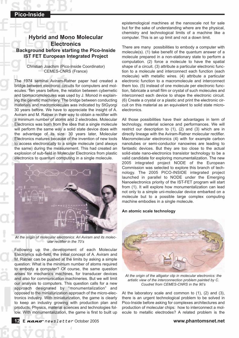
The 1974 seminal Aviram-Ratner paper had created abridge between electronic circuits for computers and mol-ecules. Ten years before, the relation between cyberneticand biomacromolecules was used by J. Monod in explain-ing the genetic machinery. The bridge between conductingmaterials and macromolecules was indicated by StGyorgi30 years before. We have to appreciate the insight of A.Aviram and M. Ratner in their way to obtain a rectifier witha minimum number of atoms and 2 electrodes. MolecularElectronics was born from the idea that a single moleculewill perform the same way a solid state device does withthe advantage of its size. 30 years later, MolecularElectronics matures because of the invention of new toolsto access electronically to a single molecule (and alwaysthe same) during the measurement. This had created anexplosion of sub-field in Molecular Electronics from plasticelectronics to quantum computing in a single molecule.
Following up the development of each MolecularElectronics sub-field, the initial concept of A. Aviram andM. Ratner can be pushed at the limits by asking a simplequestion: What is the minimum number of atoms requiredto embody a computer? Of course, the same questionarises for mechanics machines, for transducer devicesand also for communication machineries. But we will limitour analysis to computers. This question calls for a newapproach designated by “monumentalization” andopposed to the miniaturization approach of the micro-elec-tronics industry. With miniaturization, the game is clearlyto keep an industry growing with production plan andproducts. Physics, material sciences and technologies fol-low. With monumentalization, the game is first to built up
epistemological machines at the nanoscale not for salebut for the sake of understanding where are the physical,chemistry and technological limits of a machine like acomputer. This is an up limit and not a down limit.
There are many possibilities to embody a computer withmolecule(s). (1) take benefit of the quantum answer of amolecule prepared in a non-stationary state to perform acomputation. (2) force a molecule to have the spatialshape of a circuit. (3) attribute a particular electronic func-tion to a molecule and interconnect each function (eachmolecule) with metallic wires. (4) attribute a particularelectronic function to a macromolecule and interconnectthem too. (5) instead of one molecule per electronic func-tion, fabricate a small film or crystal of such molecules andinterconnect each device to shape the electronic circuit.(6) Create a crystal or a plastic and print the electronic cir-cuit on this material as an equivalent to solid state micro-electronics.
All those possibilities have their advantages in term oftechnology, material science and performances. We willrestrict our description to (1), (2) and (3) which are indirectly lineage with the Aviram-Ratner molecular rectifier.Macromolecular electronics (4) with for example carbonnanotubes or semi-conductor nanowires are leading tofantastic devices. But they are too close to the actualsolid-state nano-electronics transistor technology to be avalid candidate for exploring monumentalization. The new2005 integrated project NODE of the EuropeanCommission was selected to explore this branch of tech-nology. The 2005 PICO-INSIDE integrated projectlaunched in parallel to NODE under the EmergingNanoelectronics priority of the IST-FET program will startfrom (1). It will explore how monumentalization can leadnot only to a simple uni-molecular device embarked on amolecule but to a possible large complex computingmachine embodies in a single molecule.
An atomic scale technology
At the laboratory scale and common to (1), (2) and (3),there is an urgent technological problem to be solved inPico-Inside before asking for complexes architectures andproduction of molecular chips: how to interconnect a mol-ecule to metallic electrodes? A related problem is the
12 E newsletter October 2005 www.phantomsnet.net
At the origin of molecular electronics: Ari Aviram and its molec-ular rectifier in the 70’s
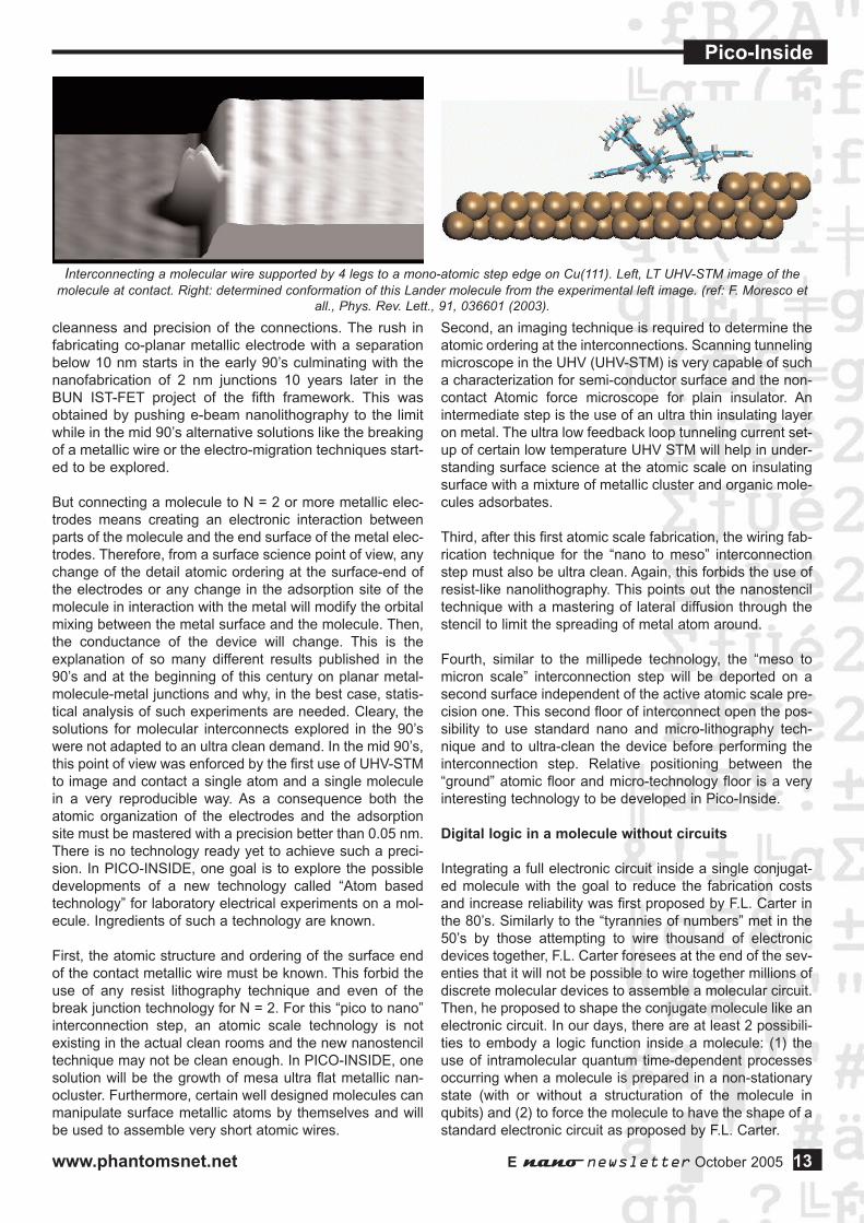
At the origin of the alligator clip in molecular electronics: theartistic view of the interconnection problem painted by C.
Coudret from CEMES-CNRS in the 90’s
Pico-Inside
cleanness and precision of the connections. The rush infabricating co-planar metallic electrode with a separationbelow 10 nm starts in the early 90’s culminating with thenanofabrication of 2 nm junctions 10 years later in theBUN IST-FET project of the fifth framework. This wasobtained by pushing e-beam nanolithography to the limitwhile in the mid 90’s alternative solutions like the breakingof a metallic wire or the electro-migration techniques start-ed to be explored.
But connecting a molecule to N = 2 or more metallic elec-trodes means creating an electronic interaction betweenparts of the molecule and the end surface of the metal elec-trodes. Therefore, from a surface science point of view, anychange of the detail atomic ordering at the surface-end ofthe electrodes or any change in the adsorption site of themolecule in interaction with the metal will modify the orbitalmixing between the metal surface and the molecule. Then,the conductance of the device will change. This is theexplanation of so many different results published in the90’s and at the beginning of this century on planar metal-molecule-metal junctions and why, in the best case, statis-tical analysis of such experiments are needed. Cleary, thesolutions for molecular interconnects explored in the 90’swere not adapted to an ultra clean demand. In the mid 90’s,this point of view was enforced by the first use of UHV-STMto image and contact a single atom and a single moleculein a very reproducible way. As a consequence both theatomic organization of the electrodes and the adsorptionsite must be mastered with a precision better than 0.05 nm.There is no technology ready yet to achieve such a preci-sion. In PICO-INSIDE, one goal is to explore the possibledevelopments of a new technology called “Atom basedtechnology” for laboratory electrical experiments on a mol-ecule. Ingredients of such a technology are known.
First, the atomic structure and ordering of the surface endof the contact metallic wire must be known. This forbid theuse of any resist lithography technique and even of thebreak junction technology for N = 2. For this “pico to nano”interconnection step, an atomic scale technology is notexisting in the actual clean rooms and the new nanostenciltechnique may not be clean enough. In PICO-INSIDE, onesolution will be the growth of mesa ultra flat metallic nan-ocluster. Furthermore, certain well designed molecules canmanipulate surface metallic atoms by themselves and willbe used to assemble very short atomic wires.
Second, an imaging technique is required to determine theatomic ordering at the interconnections. Scanning tunnelingmicroscope in the UHV (UHV-STM) is very capable of sucha characterization for semi-conductor surface and the non-contact Atomic force microscope for plain insulator. Anintermediate step is the use of an ultra thin insulating layeron metal. The ultra low feedback loop tunneling current set-up of certain low temperature UHV STM will help in under-standing surface science at the atomic scale on insulatingsurface with a mixture of metallic cluster and organic mole-cules adsorbates.
Third, after this first atomic scale fabrication, the wiring fab-rication technique for the “nano to meso” interconnectionstep must also be ultra clean. Again, this forbids the use ofresist-like nanolithography. This points out the nanostenciltechnique with a mastering of lateral diffusion through thestencil to limit the spreading of metal atom around.
Fourth, similar to the millipede technology, the “meso tomicron scale” interconnection step will be deported on asecond surface independent of the active atomic scale pre-cision one. This second floor of interconnect open the pos-sibility to use standard nano and micro-lithography tech-nique and to ultra-clean the device before performing theinterconnection step. Relative positioning between the“ground” atomic floor and micro-technology floor is a veryinteresting technology to be developed in Pico-Inside.
Digital logic in a molecule without circuits
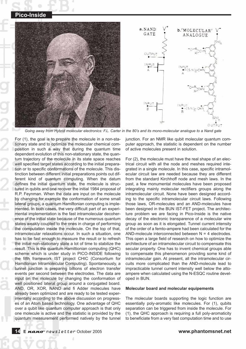
Integrating a full electronic circuit inside a single conjugat-ed molecule with the goal to reduce the fabrication costsand increase reliability was first proposed by F.L. Carter inthe 80’s. Similarly to the “tyrannies of numbers” met in the50’s by those attempting to wire thousand of electronicdevices together, F.L. Carter foresees at the end of the sev-enties that it will not be possible to wire together millions ofdiscrete molecular devices to assemble a molecular circuit.Then, he proposed to shape the conjugate molecule like anelectronic circuit. In our days, there are at least 2 possibili-ties to embody a logic function inside a molecule: (1) theuse of intramolecular quantum time-dependent processesoccurring when a molecule is prepared in a non-stationarystate (with or without a structuration of the molecule inqubits) and (2) to force the molecule to have the shape of astandard electronic circuit as proposed by F.L. Carter.
www.phantomsnet.net E newsletter October 2005 13
Interconnecting a molecular wire supported by 4 legs to a mono-atomic step edge on Cu(111). Left, LT UHV-STM image of themolecule at contact. Right: determined conformation of this Lander molecule from the experimental left image. (ref: F. Moresco et
all., Phys. Rev. Lett., 91, 036601 (2003).
Pico-Inside
For (1), the goal is to prepare the molecule in a non-sta-tionary state and to optimize the molecular chemical com-position in such a way that during the quantum timedependent evolution of this non-stationary state, the quan-tum trajectory of the molecule in its state space reacheswell specified target states according to the initial prepara-tion or to specific conformations of the molecule. This dis-tinction between different initial preparations points out dif-ferent kind of quantum computing. When the datumdefines the initial quantum state, the molecule is struc-tured in qubits and one recover the initial 1984 proposal ofR.P. Feynman. When the data are input on the moleculeby changing for example the conformation of some smalllateral groups, a quantum Hamiltonian computing is imple-mented. In both cases, the very difficult part of an experi-mental implementation is the fast intramolecular decoher-ence of the initial state because of the numerous quantumstates weakly coupled to the ones in charge of performingthe computation inside the molecule. On the top of that,intramolecular relaxations occur. In such a situation, onehas to be fast enough to measure the result or to refreshthe initial non-stationary state a lot of time to stabilize theresult. This is the quantum Hamiltionian computing (QHC)scheme which is under study in PICO-INSIDE followingthe fifth framework IST project CHIC (Consortium forHamiltonian Intramolecular Computing). Spontaneously, atunnel junction is preparing billions of electron transferevents per second between the electrodes. The data areinput on the molecule by changing the conformation ofwell positioned lateral group around a conjugated board.AND, OR, XOR, NAND and fi Adder molecules havealready been optimized and are ready to be tested exper-imentally according to the above discussion on progress-es of an Atom based technology. One advantage of QHCover a qubit like quantum computer approach is that onlyone molecule is active and the statistic is provided by thequantum measurement performed natively by the tunnel
junction. For an NMR like qubit molecular quantum com-puter approach, the statistic is dependent on the numberof active molecules present in solution.
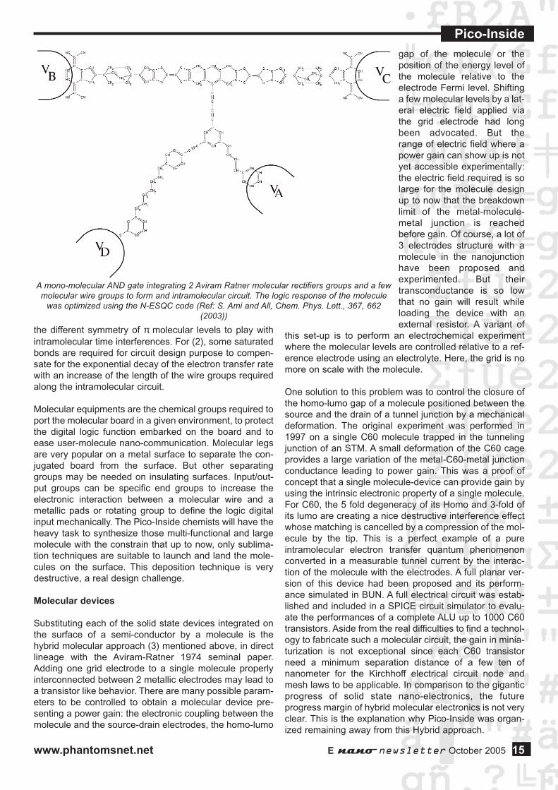
For (2), the molecule must have the real shape of an elec-trical circuit with all the node and meshes required inte-grated in a single molecule. In this case, specific intramol-ecular circuit law are needed because they are differentfrom the standard Kirchhoff node and mesh laws. In thepast, a few monumental molecules have been proposedintegrating mainly molecular rectifiers groups along theintramolecular circuit. None have been designed accord-ing to the specific intramolecular circuit laws. Followingthose laws, OR-molecules and an AND-molecules havebeen designed in the BUN IST-FET project. The architec-ture problem we are facing in Pico-Inside is the nativedecay of the electronic transparence of a molecular wiregroup as soon as it is elongated. Tunnel current intensityof the order of a femto-ampere had been calculated for theAND-molecule interconnected between N = 4 electrodes.This open a large field of research on how to optimize thearchitecture of an intramolecular circuit to compensate thissecular property. One has to invent chemical groups ableto compensate this phenomenon providing some kind ofintramolecular gain. At present, all the intramolecular cir-cuits more complicated than the AND-molecule lead toimpracticable tunnel current intensity well below the atto-ampere when calculated using the N-ESQC routine devel-oped in BUN.
Molecular board and molecular equipements
The molecular boards supporting the logic function areessentially poly-aromatic like molecules. For (1), qubitsseparation can be triggered from inside the molecule. For(1), the QHC approach is requiring a full poly-aromaticityto beneficiate from a very fast computation time and to use
14 E newsletter October 2005 www.phantomsnet.net
Going away from Hybrid molecular electronics: F.L. Carter in the 80’s and its mono-molecular analogue to a Nand gate
Pico-Inside
the different symmetry of π molecular levels to play withintramolecular time interferences. For (2), some saturatedbonds are required for circuit design purpose to compen-sate for the exponential decay of the electron transfer ratewith an increase of the length of the wire groups requiredalong the intramolecular circuit.
Molecular equipments are the chemical groups required toport the molecular board in a given environment, to protectthe digital logic function embarked on the board and toease user-molecule nano-communication. Molecular legsare very popular on a metal surface to separate the con-jugated board from the surface. But other separatinggroups may be needed on insulating surfaces. Input/out-put groups can be specific end groups to increase theelectronic interaction between a molecular wire and ametallic pads or rotating group to define the logic digitalinput mechanically. The Pico-Inside chemists will have theheavy task to synthesize those multi-functional and largemolecule with the constrain that up to now, only sublima-tion techniques are suitable to launch and land the mole-cules on the surface. This deposition technique is verydestructive, a real design challenge.
Molecular devices
Substituting each of the solid state devices integrated onthe surface of a semi-conductor by a molecule is thehybrid molecular approach (3) mentioned above, in directlineage with the Aviram-Ratner 1974 seminal paper.Adding one grid electrode to a single molecule properlyinterconnected between 2 metallic electrodes may lead toa transistor like behavior. There are many possible param-eters to be controlled to obtain a molecular device pre-senting a power gain: the electronic coupling between themolecule and the source-drain electrodes, the homo-lumo
gap of the molecule or theposition of the energy level ofthe molecule relative to theelectrode Fermi level. Shiftinga few molecular levels by a lat-eral electric field applied viathe grid electrode had longbeen advocated. But therange of electric field where apower gain can show up is notyet accessible experimentally:the electric field required is solarge for the molecule designup to now that the breakdownlimit of the metal-molecule-metal junction is reachedbefore gain. Of course, a lot of3 electrodes structure with amolecule in the nanojunctionhave been proposed andexperimented. But theirtransconductance is so lowthat no gain will result whileloading the device with anexternal resistor. A variant of
this set-up is to perform an electrochemical experimentwhere the molecular levels are controlled relative to a ref-erence electrode using an electrolyte. Here, the grid is nomore on scale with the molecule.
One solution to this problem was to control the closure ofthe homo-lumo gap of a molecule positioned between thesource and the drain of a tunnel junction by a mechanicaldeformation. The original experiment was performed in1997 on a single C60 molecule trapped in the tunnelingjunction of an STM. A small deformation of the C60 cageprovides a large variation of the metal-C60-metal junctionconductance leading to power gain. This was a proof ofconcept that a single molecule-device can provide gain byusing the intrinsic electronic property of a single molecule.For C60, the 5 fold degeneracy of its Homo and 3-fold ofits lumo are creating a nice destructive interference effectwhose matching is cancelled by a compression of the mol-ecule by the tip. This is a perfect example of a pureintramolecular electron transfer quantum phenomenonconverted in a measurable tunnel current by the interac-tion of the molecule with the electrodes. A full planar ver-sion of this device had been proposed and its perform-ance simulated in BUN. A full electrical circuit was estab-lished and included in a SPICE circuit simulator to evalu-ate the performances of a complete ALU up to 1000 C60transistors. Aside from the real difficulties to find a technol-ogy to fabricate such a molecular circuit, the gain in minia-turization is not exceptional since each C60 transistorneed a minimum separation distance of a few ten ofnanometer for the Kirchhoff electrical circuit node andmesh laws to be applicable. In comparison to the giganticprogress of solid state nano-electronics, the futureprogress margin of hybrid molecular electronics is not veryclear. This is the explanation why Pico-Inside was organ-ized remaining away from this Hybrid approach.
www.phantomsnet.net E newsletter October 2005 15
A mono-molecular AND gate integrating 2 Aviram Ratner molecular rectifiers groups and a fewmolecular wire groups to form and intramolecular circuit. The logic response of the molecule
was optimized using the N-ESQC code (Ref: S. Ami and All, Chem. Phys. Lett., 367, 662(2003))
Pico-Inside
NanoMEGAS SPRLBoulevard Edmond Machtens 79; B-1080 Brussels (Belgium)Email : [email protected] / http://www.nanomegas.com
NanoMEGAS has been created in 2004 by a team of scientists with experti-se in electron crystallography
Our products are dedicated to help the TEM user (100-400 kv) to find in an easy way the true structure (crystal parameters, symmetryand atomic positions) of nanomaterials that are otherwise impossible to determine by X-ray diffractometry or high resolution TEMmicroscopy.
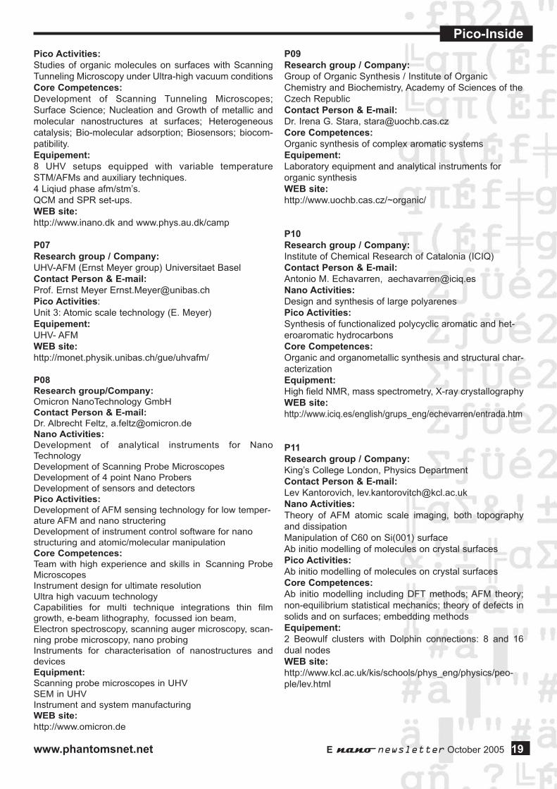
Our product “spinning star” takes control of the electron beam in a TEM and performs precession of a beam (Vincent- Midgleytechnique) in a way that one can obtain almost “kinematical” diffraction patterns.
A special dedicated software (ELD-Emap) can read and measure in automatic way intensities of ED patterns obtained with “spin-ning star”.
Spinning Star: Automatic Determination of Crystal Symmetry (K3Nb12O31F crystal)
PRECESSION ON3367 reflexions
PRECESSION OFF1786 reflexions
Starting Pico-Inside
Pico-Inside is a 3 years integratedproject whose partnership isexplained below. The Pico-Insidershave all decided to explore the mon-umentalization of a calculating unitup to the limits imposed by physics,chemistry and technology. Atomic scale technology is avery challenging path to be explored. But architecture,surface science (both experimental and theoretical) andchemistry figure also on the agenda. Pico-Insiders have todetermine if a single unique molecule can compute andcommunicate its results to the macroscopic level.
Further reading
-BUN IST-FET final Report: http://www.phantomsnet.net/Enano/euprojectreports.php
-CHIC IST-FET Project:http://www.cemes.fr/chic/
-Pico-Inside IST-FET project:http://www.picoinside.org
-C.JOACHIM, J. K. GIMZEWSKI AND A. AVIRAM, Nature,408,541 (2000)
-Molecular Electronics, Special issue of the ProceedingNational Academy of Science, USA, 102 nº25, June 21 (2005)
16 E newsletter October 2005 www.phantomsnet.net
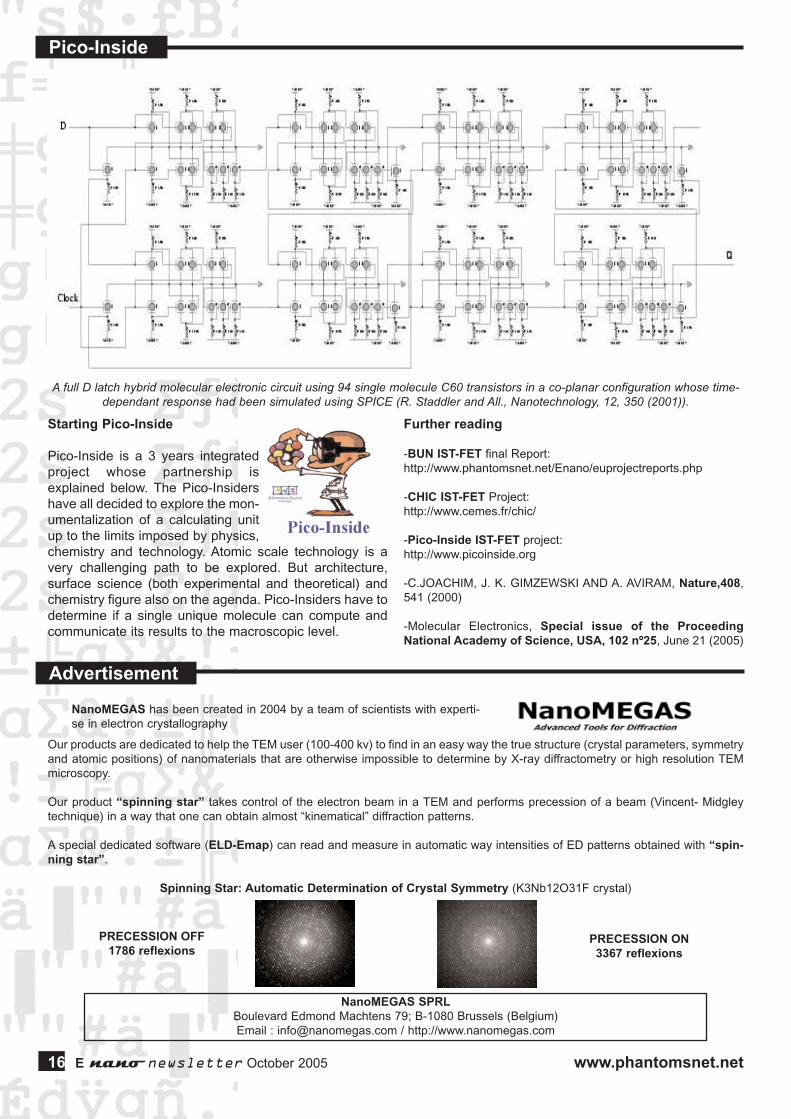
A full D latch hybrid molecular electronic circuit using 94 single molecule C60 transistors in a co-planar configuration whose time-dependant response had been simulated using SPICE (R. Staddler and All., Nanotechnology, 12, 350 (2001)).
Pico-Inside
Advertisement
Pico-Inside: Summary, Objetives andPartners
Computing inside a Single Molecule using Atomic ScaleTechnologies (Pico-Inside) is one of the new IntegratedProjects funded within the IST-FET programme (Nanoproactive initiative: http://www.cordis.lu/ist/fet/nid.htm).
Below are detailed a summa-ry of the project objectives(more info available athttp://www.picoinside.org)and a list of the partnersinvolved.
In 3 years, Pico-inside willdevelop:(1) the architecture,(2) the atomic scale technology and(3) the chemistry to explore and quantify intramolecularresources for integrating much more than a single logicgate inside a single molecule.
Five very recent breakthroughs are fully exploited by Pico-Insiders.(1) The theoretical demonstration that intramolecularquantum evolution based on the nonstationary mixing oflarge molecule quantum states can perform digital opera-tions.(2) The new intramolecular mesh and node circuit rules forlarge molecules whose internal chemical structure is sim-ilar to a standard electronic circuit architecture.(3) The experimental demonstration that the electroniccontact between a single molecular wire and its contactingatomic pad requires 0.05 nm precision.(4) The atomic resolution now obtained by a non-contactUHV-AFM on insulating surfaces and by low temperatureUHV-STM on insulator on metal systems.(5) the progresses of organic chemists to design and syn-thesise large multi-functional molecules adapted to sur-face performances at the atomic scale.
Pico-Inside integrates the necessary groups to explorenew architecture concepts with Fujitsu Europe. LT-UHV-STM and NC-UHV AFM offer a complete and true accessto the atomic scale for interconnects with Omicron. Thisincludes nano-stencil contact experiments, the necessarychemistry labs task force and the required theoreticalgroup to support the architecture, the molecular designand the analysis of Pico-Inside nanoscale experiments.This integration is completed by a true will to create anddiffuse original roadmaps to a large community aroundPico-Inside towards mono-molecular computing andatomic scale technologies.
Pico-Inside Partners:
P1.1 Centre d’Elaboration des Matériaux et d’Etudesstructurales - CEMES/CNRS (France) P1.2 Laboratoire de Physique Théorique de la MatièreCondensée / CNRS (France) P1.3 Laboratoire de Photophysique Moléculaire / CNRS(France) P2 Fujitstu Europe (France)P3 Frei Universitat Berlin (Germany)P4 Jagiellonian University (Poland)P5 Universitat Osnabrûck (Germany)P6 Aarhus Universitet (Denmark)P7 Universitaet Basel (Switzerland)P8 Omicron GmbH (Germany)P9 Institute of Organic Chemistry and Biochemistry(Czech Rep.)P10 Institute of Chemical Research of Catalonia - ICIQ(Spain)P11 King’s College London (UK)P12 University College London - UCL (UK)P13 Phantoms Foundation (Spain)
P1.1Research group / Company:GNS-CEMES/CNRSContact Person & E-mail:[email protected], [email protected],[email protected] Activities:Design and synthesis of uni-molecular machines,intramolecular logic gatesESQC STM image interpretation, intramolecular circuittheory, UHV NanostencilPico Activities:LT-UHV-STM, 5 pm noiseContact conductance optimisation with a precision betterthan 0.05 nmCore Competences:Molecular design and synthesis, UHV-STM, NC-AFMNanostencilEquipement:2 UHV-STM, LT-UHV STM, NC-AFMWEB site:http://www.cemes.fr/GNS/
P1.2Research group / Company:Laboratoire de physique théorique de la matière conden-sée, Université Pierre et Marie Curie et CNRS Paris,FranceContact Person & E-mail:Rémy Mosseri, [email protected] Competences:Theory: solid state physics - quantum informationEquipement:ComputersWEB site:http://www.lptl.jussieu.fr/
www.phantomsnet.net E newsletter October 2005 17
Pico-Inside
P1.3Research group / Company:Molecular nanoscience group, Laboratoire dePhotophysique Moléculaire (Orsay), FranceContact person:Dr. Gérald Dujardin, [email protected] activities:Local electronic excitation of single molecules andnanocrystals by using STM, conducting AFM and com-bined laser+STM. Electronic control of dynamics andluminscence of individual molecules and nanocrystals.Picometer-scale electronic control of molecular dynamicsinside a single moleculeM. Lastapis, M. Martin, D. Riedel, L. Hellner, G. Comtet,G. Dujardin Science 308, 1000 (2005)Core competences:STM, AFM and Laser+STM manipulations of individualmolecules and nanocrystals. Atomic-scale studies on wideband gap semiconductor surfaces. Molecular nano-machines, movement and luminescence.Equipment:UHV room temperature STM, UHV variable temperatureSTM, UHV low temperature (5K) STM, laser+STM, airAFM.Web site:http://voyager.ppm.u-psud.fr/nanophysics/nanophysics.html
P02Research group / Company:Fujitstu Systems Europe, FranceContact Person & E-mail:Pierre Lagier - [email protected] Latour - [email protected] Activities:Image synthesis, architecturePico Activities:Architectures for mono-molecular electronicsChemistryCore Competences:computer science, physicsEquipement:ComputersWEB site:http://www.fujitsu.com
P03Research group / Company:Institut fuer Experimentalphysik, Freie Universitaet Berlin Contact Person & E-mail:Francesca Moresco, [email protected] Activities:Manipulation of single molecule on metal surfaces.Contacting single molecules between nanoelectrodes.Core Competences:Low Temperature STM, manipulation of atoms and mole-culesEquipement:Scanning Tunneling Microscopes working at 5KWEB site: http://www.physik.fu-berlin.de/~ag-rieder/LT-STM2
P04Research group/Company:Centre for Nanometer-scale Science and AdvancedMaterials (NANOSAM) at the Institute of Physics,Jagiellonian University, Krakow, PolandContact Person & E-mail:Prof. Marek Szymonski, [email protected] activities:UHV-STM on semiconducting surfaces; UHV-NC AFM onsemiconducting and bulk insulator surfaces; Metallurgy ofnanoscopic mesa padsCore Competences:Preparation and investigation of surfaces of III-V semicon-ductors and ionic insulators, preparation of insulator/metalthin films/nanostructures on semiconductors, NC-AFM,ion/electron induced desorption/sputteringEquipment:UHV STM/NCAFM, UHV LT-STM, AES, LEED, XPS,SNMS, QMS, multi-technique surface analysis and MBEsystems, ambient AFM/STM microscopes Web site:http://www.if.uj.edu.pl/NANOSAM/
P05Research group / Company:NanoScience / Universität OsnabrückContact Person & E-mail:Michael Reichling, [email protected] Activities:Imaging and manipulation of molecular assemblies andultra-thin filmsPico Activities:Characterization and manipulation of internal molecularstructures and conformationCharacterization of the bonding of molecules to substratesand contactsCore Competences:Atomic resolution force microscopyImaging and manipulation of insulating surfaces andnanostructuresImaging and manipulation of molecules and ultra-thin filmsEquipment:Ultra-high vacuum force microscopes operated at Room temperature, variable temperature and cryogenictemperatureWEB site:http://reichling.physik.uos.de/
P06Research group / Company:SPM group, Interdisciplinary Nanoscience Center(iNANO), University of Aarhus, DenmarkContact Person & E-mail:Flemming Besenbacher, [email protected] Activities:Development of High resolution Scanning ProbeMicroscopes.SPM studies of molecular adsorption and self-assembly,heterogenous catalysis and metal growth.Development of biosensors and biocompatible implants.
18 E newsletter October 2005 www.phantomsnet.net
Pico-Inside
Pico Activities:Studies of organic molecules on surfaces with ScanningTunneling Microscopy under Ultra-high vacuum conditionsCore Competences:Development of Scanning Tunneling Microscopes;Surface Science; Nucleation and Growth of metallic andmolecular nanostructures at surfaces; Heterogeneouscatalysis; Bio-molecular adsorption; Biosensors; biocom-patibility.Equipement:8 UHV setups equipped with variable temperatureSTM/AFMs and auxiliary techniques.4 Liqiud phase afm/stm’s.QCM and SPR set-ups. WEB site:http://www.inano.dk and www.phys.au.dk/camp
P07Research group / Company:UHV-AFM (Ernst Meyer group) Universitaet BaselContact Person & E-mail:Prof. Ernst Meyer [email protected] Activities:Unit 3: Atomic scale technology (E. Meyer)Equipement:UHV- AFMWEB site:http://monet.physik.unibas.ch/gue/uhvafm/
P08Research group/Company:Omicron NanoTechnology GmbHContact Person & E-mail:Dr. Albrecht Feltz, [email protected] Activities: Development of analytical instruments for NanoTechnologyDevelopment of Scanning Probe MicroscopesDevelopment of 4 point Nano ProbersDevelopment of sensors and detectorsPico Activities: Development of AFM sensing technology for low temper-ature AFM and nano structeringDevelopment of instrument control software for nanostructuring and atomic/molecular manipulationCore Competences: Team with high experience and skills in Scanning ProbeMicroscopesInstrument design for ultimate resolutionUltra high vacuum technologyCapabilities for multi technique integrations thin filmgrowth, e-beam lithography, focussed ion beam, Electron spectroscopy, scanning auger microscopy, scan-ning probe microscopy, nano probingInstruments for characterisation of nanostructures anddevicesEquipment: Scanning probe microscopes in UHVSEM in UHVInstrument and system manufacturingWEB site:http://www.omicron.de
P09Research group / Company:Group of Organic Synthesis / Institute of OrganicChemistry and Biochemistry, Academy of Sciences of theCzech RepublicContact Person & E-mail:Dr. Irena G. Stara, [email protected] Competences:Organic synthesis of complex aromatic systemsEquipement:Laboratory equipment and analytical instruments fororganic synthesisWEB site:http://www.uochb.cas.cz/~organic/
P10Research group / Company:Institute of Chemical Research of Catalonia (ICIQ)Contact Person & E-mail:Antonio M. Echavarren, [email protected] Activities:Design and synthesis of large polyarenesPico Activities:Synthesis of functionalized polycyclic aromatic and het-eroaromatic hydrocarbonsCore Competences:Organic and organometallic synthesis and structural char-acterizationEquipment:High field NMR, mass spectrometry, X-ray crystallographyWEB site:http://www.iciq.es/english/grups_eng/echevarren/entrada.htm
P11Research group / Company:King’s College London, Physics DepartmentContact Person & E-mail:Lev Kantorovich, [email protected] Activities:Theory of AFM atomic scale imaging, both topographyand dissipationManipulation of C60 on Si(001) surfaceAb initio modelling of molecules on crystal surfacesPico Activities:Ab initio modelling of molecules on crystal surfacesCore Competences:Ab initio modelling including DFT methods; AFM theory;non-equilibrium statistical mechanics; theory of defects insolids and on surfaces; embedding methodsEquipement:2 Beowulf clusters with Dolphin connections: 8 and 16dual nodesWEB site:http://www.kcl.ac.uk/kis/schools/phys_eng/physics/peo-ple/lev.html
www.phantomsnet.net E newsletter October 2005 19
Pico-Inside

P12Research group / Company:London Centre for Nanotechnology, University CollegeLondonContact Person & E-mail:Professor Alexander Shluger, [email protected] Activities:Modelling of defect structure and defect processes in gateoxide materials for nano-CMOS devices; modelling of con-trast formation in Atomic Force Microscopy on insulatingsurfaces; theoretical studies of the mechanisms of manip-ulation of nano-structures (clusters and molecules) atinsulating surfaces; modelling of adsorption and diffusionof molecular species at insulating surfaces; mechanismsof photo-induced processes in nano-clusters.Pico Activities:Adsorption, structure, diffusion and manipulation of proto-type molecules for molecular electronic devices at insulat-ing substrates; effect of current and charging on the struc-ture, stability and diffusion of adsorbed molecules.Core competences:Development and application of computational methodsfor theoretical modelling of atomic and electronic process-es in the bulk and at surfaces of insulators.Equipment:ComputersWEB site:http://www.cmmp.ucl.ac.uk/
P13Research group / Company:Phantoms FoundationContact Person & E-mail:Dr. Antonio Correia, [email protected] Core Competences:NanoelectronicsTeam with high experience and skills in project manage-ment and scientific conference organisation WEB site:http://www.phantomsnet.net
For more information about Pico-Inside Project, pleasevisit the related web site at: http://www.picoinside.org
Pico-Inside logo courtesy: MIDAM Production sprl18, rue du Verger. 1950 Kraainem Belgique
20 E newsletter October 2005 www.phantomsnet.net
Pico-Inside
Don't miss the opportunity to advertise in E-NANO Newsletter!
Launched in 2005, E-NANO Newsletter is published fourtimes a year and distributed among 1000 research labsin Europe. This newsletter brings readers the latestnews, research articles and resources from theNanotechnology world.
ADVERTISING RATES
Option 1: E-Nano Newsletter - 1 page advert full colourYour Company advert in the E-Nano Newsletter:1 page ad / 4 issues: 700 Euros1 page ad / 2 issues: 500 Euros1 page ad / 1 issue: 400 Euros
Option 2: E-Nano Newsletter - 1/2 page advert fullcolourYour Company advert in the E-Nano Newsletter:1/2 page ad / 4 issues: 600 Euros1/2 page ad / 2 issues: 400 Euros1/2 page ad / 1 issue: 300 Euros
Option 3: E-Nano Newsletter - 1/4 page advert fullcolourYour Company advert in the E-Nano Newsletter:1/4 page ad / 4 issues: 500 Euros1/4 page ad / 2 issues: 300 Euros1/4 page ad / 1 issue: 200 Euros
More information
Adverts in Black and White: 15% discountSpecified positions (including inside front page, inside
back cover and back page), please add 15% to theadvertisement rates.
Ads must be supplied by advertisers.Rates do not include VAT (16%).
For more details on advertising, please contact us by E-mail ([email protected]) or fax (+34 914973471).
Current E-NANO Newsletter Ads
NANO News - http://www.phantomsnet.net/Resources/news.php
MONA EU funded project to coordinate optics and nanotechnology research [03-10-2005]
A new IST project has been launched that will contribute to the coordination of research in photonics and nanotechno-logies
Nanophotonics & Nano-Optoelectronics
MINATEC and Trends in Nanotechnology Conference series will join forces to organise 2006 event in Grenoble(France) [28-09-2005]
TNT2006 (www.tnt2006.org) is been launched following the overwhelming success of earlier NanotechnologyConferences. The TNT2006 edition will be organised out of Spain for the first time - Grenoble (France) - to emphasisethe importance at the European level of the launch of the Centre of Innovation in Micro and Nanotechnology, MINA-TEC.
Nanoelectronics, Nanobiotechnology, Scientific Policy
CEA initiates the first French nanobiotech cluster in Grenoble [28-09-2005]
CEA announces the creation of the first French nanobiotechnology cluster. The official launch was made on September9th with the signature of a real estate operation dedicated to host new equipments and research teams in Grenobleclose to the Minatec facilities.
Nanobiotechnology
Detailed plans for implementing the Seventh Framework Programme (FP7) [22-09-2005]
On 21 September 2005 the European Commission approved its detailed plans for implementing the SeventhFramework Programme (FP7). Provisional versions of the Specific Programmes - the four pillars of Cooperation, Ideas,People and Capacities, as well as research under Euratom and by the JRC under Euratom and EC treaties - are nowavailable.
Scientific Policy
Measuring Nanotube’s Conductivity [06-09-2005]
Hongjie Dai and his colleagues at Stanford have made the first electrical measurements of currents flowing under highvoltage (high bias) through single-walled carbon nanotubes suspended like miniature power lines.
Nanotubes
Launch of the European Technology Platform on NanoMedicine [06-09-2005]
NanoMedicine is defined as the application of Nanotechnology to Health. It exploits the improved and often novel physi-cal, chemical, and biological properties of materials at the nanometric scale. NanoMedicine has potential impact on theprevention, early and reliable diagnosis and treatment of diseases.
Nanomedicine, Scientific Policy
www.phantomsnet.net E newsletter October 2005 21
NANO News
Intel Drives Moore's Law Forward With 65 Nanometer Process Technology [30-08-2005]
A significant milestone in developing next-generation chip manufacturing technology has been achieved by IntelCorporation. The company has built fully functional 70-megabit static random access memory (SRAM) chips with morethan half a billion transistors using the world's most advanced 65 nanometer (nm) process technology.
Nanoelectronics, Nanofabrication
Boosting Europe’s semiconductor research [18-08-2005]
Though Europe's top semiconductor research centres are separated by hundreds of miles they could unite in a vast,distributed R&D network thanks to the work of a EU-funded project.
Nanosensors & Nanodevices, Scientific Policy
EU funded projects resulting from the Emerging Nanoelectronics Call [14-08-2005]
The FET “Nano” initiative complements mainstream IC developments with advanced research in hybrid and molecularelectronics, and prepares the bases for an extension of integrated circuit technology beyond the limits of CMOS sca-ling. This initiative covers a time horizon beyond 2009, corresponding to that covered in the "Emerging ResearchDevices" (ERD) section of the ITRS roadmap. The scope is however limited to a number of non-CMOS options listedin the ERD document.
Nanoelectronics, Molecular Electronics, Scientific Policy
Contacting single molecules [11-08-2005]
The field of molecular electronics has so far developed relatively slowly. But now researchers at the Weizmann Instituteof Science (Israel) have come up with a method for contacting single molecules more reliably.
Molecular Electronics
Templates yield nano branches [10-08-2005]
Researchers from Rensselaer Polytechnic Institute have devised a way to make highly branched nanostructures frommany different types of materials.
Molecular Electronics, Nanotubes, Nanofabrication
Carbon nanotubes sort themselves out [09-08-2005]
Researchers have come up with a technique that could sort carbon nanotubes according to their length. Applying ashear stress to a suspension of multiwalled carbon nanotubes caused shorter tubes to move towards the walls whilelonger tubes headed for the middle of the container.
Nanotubes
NanoImprint Lithography Impact [04-08-2005]
Nanoimprint lithography offers an economical, high-resolution alternative to EUV and next-generation lithography.
Nanofabrication, Nanolithography, Nanoimprint
22 E newsletter October 2005 www.phantomsnet.net
NANO News
(November 2005)
NanoSolutions 20058-10 November 2005Köln, Germanyhttp://www.nanosolutions-cologne.com
2nd International Symposium on Nanotechnology in Construction13-16 November 2005Bilbao, Bizkaia, Spainhttp://www.mmsconferencing.com/nanoc/
Veeco UK Scanning Probe Microscopy Conference and User Meeting22-23 November 2005Oxford, Oxfordshire, United Kingdomhttp://www.veeco-europe.com/others.news.users-meetings.102.cescreen
BioNanoMAT: Bioinspired Nanomaterials for Medicine and Technologies23-24 November 2005Marl, Germanyhttp://events.dechema.de/bionanomat.html
(December 2005)
International Symposium on Molecular Electronics05-06 December 2005Tsukuba, Japanhttp://www.nanoworld.jp/mole/index.php
Micro and Nanotechnology 2005 (MNT 05)12-14 December 2005London, United Kingdomhttp://www.iom3.org/events/mnt2005.htm
Towards Molecular Electronics: 5th International Conference on Advanced Materials and Nanotechnology12-17 December 2005Srem, Polandhttp://main2.amu.edu.pl/~tme/
European Nano Systems 200514-16 December 2005Paris, Francehttp://tima.imag.fr/conferences/ENS/
Second Meeting on Molecular Electronic Elecmol´0519-21 December, 2005Grenoble Joseph Fourier University (France)http://www.elecmol.org/
(January 2006)
NanoSingapore 2006: IEEE Conference on Emerging Technologies – Nanoelectronics10-13 January, 2006Singaporehttp://www.ieeecet.org/
www.phantomsnet.net E newsletter October 2005 23
NANO Conferences
Post-doctoral Position: "Functional Polymers within Organic and Biomolecular Electronics"
Research in the field of experimental soft condensed matter physics and chemistry, with particular emphasis on func-tional polymers within organic and biomolecular electronics. Research duties will include participation in a EuropeanFP6 integrated project (NaPa) on emerging nanopatterning methods. The position includes responsibility for research tutoring and administrative tasks.
More information on the announced position could be given by professor Olle Inganäs, e-mail: [email protected], tel. no.+46 13 28 12 31. The union representative is Per Larsson (SACO), e-mail [email protected], tel. no. +46 708 28 1102. The application should be sent to Linköpings universitet, IFM, Ingmarie Åkesson, SE-581 83 Linköping, Sweden.
10 PhD Positions: "CHEMTRONICS - Chemistry and Nanoelectronics"
This training project for 10 PhD students during 3 years,in the frame of the MINATEC innovation center (Grenoble,France), will allow a better coupling both between chemistry and nanoelectronicsand between scientific and technolo-gical research. It will favour a multicultural approachso that experts, researchers, engineers and students can run ortake part to multidisciplinary projects, which are crucial for the future of nanoelectronics.
To get additionnal information, please send a mail to : [email protected]. To apply, please send a CV, a letter ofmotivation, two letters of recommendation, a copy of the last diploma, and a list of publications.
PhD Project Studentships in Nanotechnology: Nanomanipulation, Nanomechanics and 3D Reconstruction
Department of Engineering Materials, University of SheffieldFully funded PhD project studentships are available for immediate application, inclusive of overseas candidates, withany start date between now and 1st Jan 2006.The research area covers Focused Ion Beam microscopy for nanoscale patterning and imaging, nanoindentation stu-dies with high spatial resolution, mechanical properties of MEMS/NEMS devices, 3D Reconstruction of nanoobjectsby tomographic techniques, characterisation of nanoporous and nanocomposite materials.
Please send your CV and statement of interests plus name of at least 2 referees to Dr G Moebus, [email protected],Dept of Engineering Materials, University of Sheffield, Sheffield S1 3JD, UK.The Sheffield University prospectus can be found on http://www.sheffield.ac.uk/apply/research.html
3 Year Research Position: "New frontiers of surface molecular assemblies and organic-based nano-architec-tures"
The National Nanotechnology Laboratory is seeking for a research scientist to investigate the new frontiers of surfacemolecular assemblies and organic-based nano-architectures.The 3 years research project will be focused on a wide range of micropatterned devices based on surface chemistry,self-assembly of organic molecules, polymers, and proteins on surfaces, for MEMS and microfluidic applications.Candidates should have an excellent experimental background in polymer chemistry, supramolecular chemistry, orga-nic synthesis, materials science, nano-science, surface functionalization, and surface and colloid chemistry. Excellentability in writing and conversation in English is strongly required.The applicants should have a PhD in chemistry, chemical physics, materials science, or experimental condensed-matter physics.We welcome applicants who have one or two year postdoctoral experience. Applicants should submit a full CV to:Dr. Dario PisignanoNational Nanotechnology Laboratory CNR- INFM - Universita' di Leccec/o Palazzine Garrisi; via Arnesano - I-73100 Lecce (Italy)Phone +39 0832298146FAX +39 0832298238E-mail [email protected]
24 E newsletter October 2005 www.phantomsnet.net
NANO Vacancies
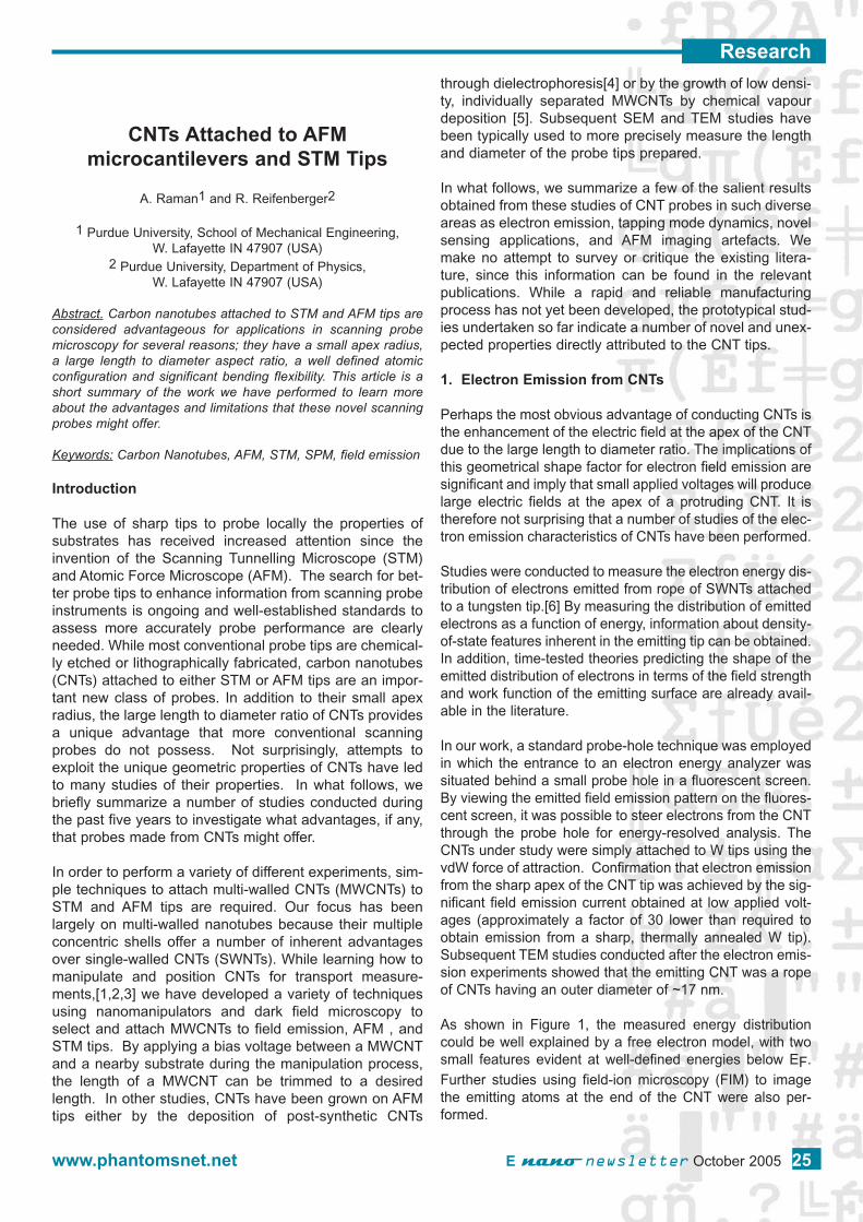
CNTs Attached to AFMmicrocantilevers and STM Tips
A. Raman1 and R. Reifenberger2
1 Purdue University, School of Mechanical Engineering, W. Lafayette IN 47907 (USA)
2 Purdue University, Department of Physics, W. Lafayette IN 47907 (USA)
Abstract. Carbon nanotubes attached to STM and AFM tips areconsidered advantageous for applications in scanning probemicroscopy for several reasons; they have a small apex radius,a large length to diameter aspect ratio, a well defined atomicconfiguration and significant bending flexibility. This article is ashort summary of the work we have performed to learn moreabout the advantages and limitations that these novel scanningprobes might offer.
Keywords: Carbon Nanotubes, AFM, STM, SPM, field emission
Introduction
The use of sharp tips to probe locally the properties ofsubstrates has received increased attention since theinvention of the Scanning Tunnelling Microscope (STM)and Atomic Force Microscope (AFM). The search for bet-ter probe tips to enhance information from scanning probeinstruments is ongoing and well-established standards toassess more accurately probe performance are clearlyneeded. While most conventional probe tips are chemical-ly etched or lithographically fabricated, carbon nanotubes(CNTs) attached to either STM or AFM tips are an impor-tant new class of probes. In addition to their small apexradius, the large length to diameter ratio of CNTs providesa unique advantage that more conventional scanningprobes do not possess. Not surprisingly, attempts toexploit the unique geometric properties of CNTs have ledto many studies of their properties. In what follows, webriefly summarize a number of studies conducted duringthe past five years to investigate what advantages, if any,that probes made from CNTs might offer.
In order to perform a variety of different experiments, sim-ple techniques to attach multi-walled CNTs (MWCNTs) toSTM and AFM tips are required. Our focus has beenlargely on multi-walled nanotubes because their multipleconcentric shells offer a number of inherent advantagesover single-walled CNTs (SWNTs). While learning how tomanipulate and position CNTs for transport measure-ments,[1,2,3] we have developed a variety of techniquesusing nanomanipulators and dark field microscopy toselect and attach MWCNTs to field emission, AFM , andSTM tips. By applying a bias voltage between a MWCNTand a nearby substrate during the manipulation process,the length of a MWCNT can be trimmed to a desiredlength. In other studies, CNTs have been grown on AFMtips either by the deposition of post-synthetic CNTs
through dielectrophoresis[4] or by the growth of low densi-ty, individually separated MWCNTs by chemical vapourdeposition [5]. Subsequent SEM and TEM studies havebeen typically used to more precisely measure the lengthand diameter of the probe tips prepared.
In what follows, we summarize a few of the salient resultsobtained from these studies of CNT probes in such diverseareas as electron emission, tapping mode dynamics, novelsensing applications, and AFM imaging artefacts. Wemake no attempt to survey or critique the existing litera-ture, since this information can be found in the relevantpublications. While a rapid and reliable manufacturingprocess has not yet been developed, the prototypical stud-ies undertaken so far indicate a number of novel and unex-pected properties directly attributed to the CNT tips.
1. Electron Emission from CNTs
Perhaps the most obvious advantage of conducting CNTs isthe enhancement of the electric field at the apex of the CNTdue to the large length to diameter ratio. The implications ofthis geometrical shape factor for electron field emission aresignificant and imply that small applied voltages will producelarge electric fields at the apex of a protruding CNT. It istherefore not surprising that a number of studies of the elec-tron emission characteristics of CNTs have been performed.
Studies were conducted to measure the electron energy dis-tribution of electrons emitted from rope of SWNTs attachedto a tungsten tip.[6] By measuring the distribution of emittedelectrons as a function of energy, information about density-of-state features inherent in the emitting tip can be obtained.In addition, time-tested theories predicting the shape of theemitted distribution of electrons in terms of the field strengthand work function of the emitting surface are already avail-able in the literature.
In our work, a standard probe-hole technique was employedin which the entrance to an electron energy analyzer wassituated behind a small probe hole in a fluorescent screen.By viewing the emitted field emission pattern on the fluores-cent screen, it was possible to steer electrons from the CNTthrough the probe hole for energy-resolved analysis. TheCNTs under study were simply attached to W tips using thevdW force of attraction. Confirmation that electron emissionfrom the sharp apex of the CNT tip was achieved by the sig-nificant field emission current obtained at low applied volt-ages (approximately a factor of 30 lower than required toobtain emission from a sharp, thermally annealed W tip).Subsequent TEM studies conducted after the electron emis-sion experiments showed that the emitting CNT was a ropeof CNTs having an outer diameter of ~17 nm.
As shown in Figure 1, the measured energy distributioncould be well explained by a free electron model, with twosmall features evident at well-defined energies below EF.Further studies using field-ion microscopy (FIM) to imagethe emitting atoms at the end of the CNT were also per-formed.
www.phantomsnet.net E newsletter October 2005 25
Research
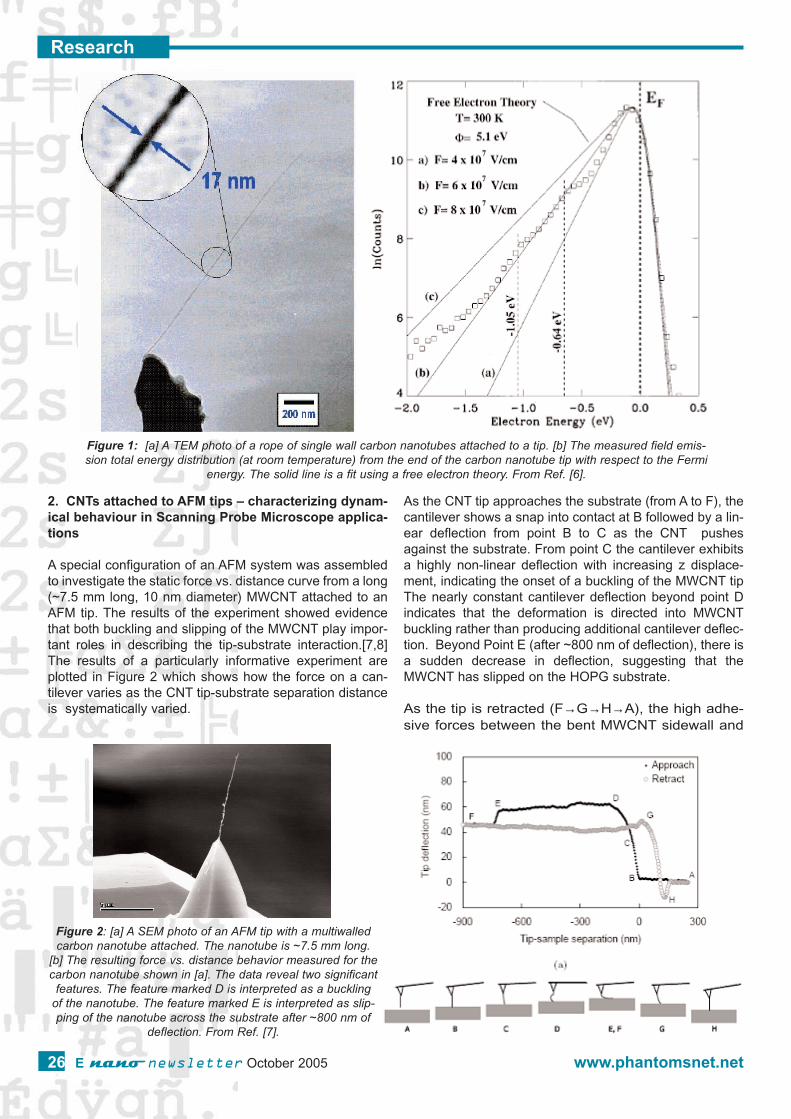
2. CNTs attached to AFM tips – characterizing dynam-ical behaviour in Scanning Probe Microscope applica-tions
A special configuration of an AFM system was assembledto investigate the static force vs. distance curve from a long(~7.5 mm long, 10 nm diameter) MWCNT attached to anAFM tip. The results of the experiment showed evidencethat both buckling and slipping of the MWCNT play impor-tant roles in describing the tip-substrate interaction.[7,8]The results of a particularly informative experiment areplotted in Figure 2 which shows how the force on a can-tilever varies as the CNT tip-substrate separation distanceis systematically varied.
As the CNT tip approaches the substrate (from A to F), thecantilever shows a snap into contact at B followed by a lin-ear deflection from point B to C as the CNT pushesagainst the substrate. From point C the cantilever exhibitsa highly non-linear deflection with increasing z displace-ment, indicating the onset of a buckling of the MWCNT tipThe nearly constant cantilever deflection beyond point Dindicates that the deformation is directed into MWCNTbuckling rather than producing additional cantilever deflec-tion. Beyond Point E (after ~800 nm of deflection), there isa sudden decrease in deflection, suggesting that theMWCNT has slipped on the HOPG substrate.
As the tip is retracted (F→G→H→A), the high adhe-sive forces between the bent MWCNT sidewall and
26 E newsletter October 2005 www.phantomsnet.net
Figure 2: [a] A SEM photo of an AFM tip with a multiwalledcarbon nanotube attached. The nanotube is ~7.5 mm long.
[b] The resulting force vs. distance behavior measured for thecarbon nanotube shown in [a]. The data reveal two significant
features. The feature marked D is interpreted as a bucklingof the nanotube. The feature marked E is interpreted as slip-ping of the nanotube across the substrate after ~800 nm of
deflection. From Ref. [7].
Figure 1: [a] A TEM photo of a rope of single wall carbon nanotubes attached to a tip. [b] The measured field emis-sion total energy distribution (at room temperature) from the end of the carbon nanotube tip with respect to the Fermi
energy. The solid line is a fit using a free electron theory. From Ref. [6].
Research

the substrate ensures that the cantilever deflectionremains nearly constant from F to G. From G to H the stat-ic force distance curve is similar to that during approachfrom B to D, albeit in the reverse order. Due to thermaldrifts in the z position, the data between B to D and G toH do not exactly coincide. This static force vs. distancedata were repeated several times with similar qualitativeand quantitative results.
We have shown that the static force distance curvedescribed here influences directly the dynamic behaviourin Tapping Mode AFM using this tip [7,8]. In particular wehave demonstrated using theoretical models and carefulexperiments that the co-existence of attractive and repul-sive regime imaging is strongly correlated to the bucklingproperties of the CNT tip. Because the buckling propertiesof CNT’s are strongly influenced by their lengths, we arein the process of systematically investigating the effects ofCNT length on the dynamic response of the CNT AFMprobes.
3. CNTs attached to AFM Cantilevers – Novel Sensors
In an effort to harness the high mass sensitivity inherent incarbon nanotube resonators, we have investigated exper-imentally and analytically the unusual coupled vibrationcharacteristics of MWCNTs suspended from flexiblemicrocantilevers (CNT “whiskered” cantilever sensors).The advantage of this approach is that by monitoring thedifferent vibrational resonances of the microcantilever, it is
possible to gain information about the vibrational proper-ties of the attached CNT. We have found that the additionof a gauge mass to the free end of the CNT changes dra-matically the coupled vibration characteristics of the sys-tem and unexpectedly increases some of the cantileverresonance frequencies.[9] This non-intuitive behavior isshown to arise as a natural consequence of curve veeringin coupled eigenvalue problems, and impacts directly thepossibility of small mass detection using such whiskeredcantilever sensors.
www.phantomsnet.net E newsletter October 2005 27
Figure 3: A MWCNT nanotube attached to an AFM microcan-tilever. By studying the motion of the microcantilever, informa-tion about the dynamics of the nanotube can be inferred. As anexample, a particle (mass ~10 pg) has been intentionally addedto the end of the nanotube to learn more about the vibrational
dynamics of the nanotube itself. From Ref. [9]
Scanning Probe Microscopy (SPM) systems offered by NanoTec include STM, SFM, as well as versatile digital con-trol electronic units for any kind of SPM (including home-built systems).
Our systems allow a large variety of operation modes: Spectroscopy, DSFM, ESFM, MFM, Jumping Mode, 3D-Modes, CITS, 2nd Feedback, NanoLithography...
WSxM, the freeware SPM program, controls all these features and much more. In addition, you can usethis program to analyse data from most commercial SPM systems.
We think WSxM is the best data acquisition & image processing SPM software on the market.
Free download , try it,and let us know your opinion.
Internet: http://www.nanotec.ese-mail:[email protected]
http://www.nanotec.es
NANOTEC ELECTRONICA
Take a look at the nanoworld
Take a look at NANOTEC
NanoTec develops powerful tools for visualizing and manipulating the NanoWorld
Research
Advertisement
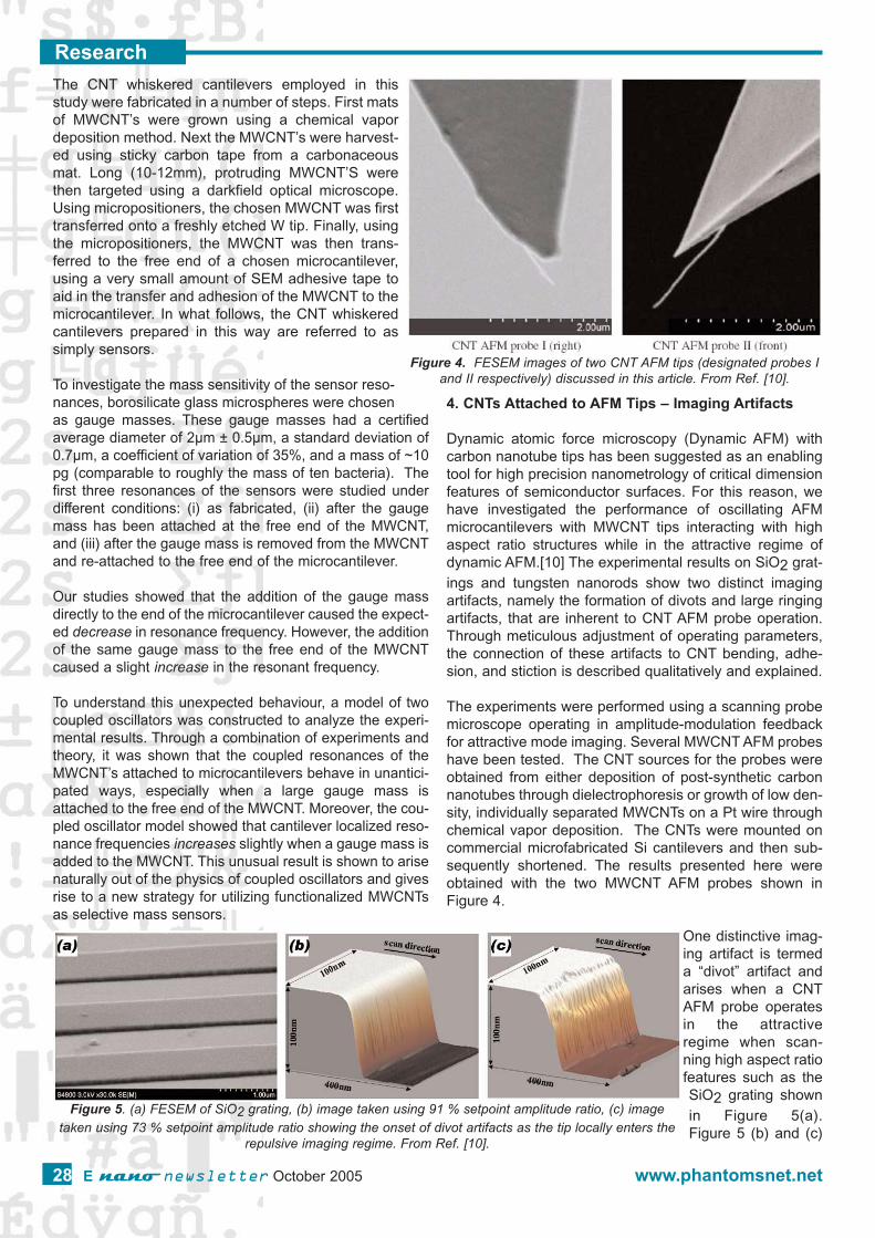
The CNT whiskered cantilevers employed in thisstudy were fabricated in a number of steps. First matsof MWCNT’s were grown using a chemical vapordeposition method. Next the MWCNT’s were harvest-ed using sticky carbon tape from a carbonaceousmat. Long (10-12mm), protruding MWCNT’S werethen targeted using a darkfield optical microscope.Using micropositioners, the chosen MWCNT was firsttransferred onto a freshly etched W tip. Finally, usingthe micropositioners, the MWCNT was then trans-ferred to the free end of a chosen microcantilever,using a very small amount of SEM adhesive tape toaid in the transfer and adhesion of the MWCNT to themicrocantilever. In what follows, the CNT whiskeredcantilevers prepared in this way are referred to assimply sensors.
To investigate the mass sensitivity of the sensor reso-nances, borosilicate glass microspheres were chosenas gauge masses. These gauge masses had a certifiedaverage diameter of 2µm ± 0.5µm, a standard deviation of0.7µm, a coefficient of variation of 35%, and a mass of ~10pg (comparable to roughly the mass of ten bacteria). Thefirst three resonances of the sensors were studied underdifferent conditions: (i) as fabricated, (ii) after the gaugemass has been attached at the free end of the MWCNT,and (iii) after the gauge mass is removed from the MWCNTand re-attached to the free end of the microcantilever.
Our studies showed that the addition of the gauge massdirectly to the end of the microcantilever caused the expect-ed decrease in resonance frequency. However, the additionof the same gauge mass to the free end of the MWCNTcaused a slight increase in the resonant frequency.
To understand this unexpected behaviour, a model of twocoupled oscillators was constructed to analyze the experi-mental results. Through a combination of experiments andtheory, it was shown that the coupled resonances of theMWCNT’s attached to microcantilevers behave in unantici-pated ways, especially when a large gauge mass isattached to the free end of the MWCNT. Moreover, the cou-pled oscillator model showed that cantilever localized reso-nance frequencies increases slightly when a gauge mass isadded to the MWCNT. This unusual result is shown to arisenaturally out of the physics of coupled oscillators and givesrise to a new strategy for utilizing functionalized MWCNTsas selective mass sensors.
4. CNTs Attached to AFM Tips – Imaging Artifacts
Dynamic atomic force microscopy (Dynamic AFM) withcarbon nanotube tips has been suggested as an enablingtool for high precision nanometrology of critical dimensionfeatures of semiconductor surfaces. For this reason, wehave investigated the performance of oscillating AFMmicrocantilevers with MWCNT tips interacting with highaspect ratio structures while in the attractive regime ofdynamic AFM.[10] The experimental results on SiO2 grat-ings and tungsten nanorods show two distinct imagingartifacts, namely the formation of divots and large ringingartifacts, that are inherent to CNT AFM probe operation.Through meticulous adjustment of operating parameters,the connection of these artifacts to CNT bending, adhe-sion, and stiction is described qualitatively and explained.
The experiments were performed using a scanning probemicroscope operating in amplitude-modulation feedbackfor attractive mode imaging. Several MWCNT AFM probeshave been tested. The CNT sources for the probes wereobtained from either deposition of post-synthetic carbonnanotubes through dielectrophoresis or growth of low den-sity, individually separated MWCNTs on a Pt wire throughchemical vapor deposition. The CNTs were mounted oncommercial microfabricated Si cantilevers and then sub-sequently shortened. The results presented here wereobtained with the two MWCNT AFM probes shown inFigure 4.
One distinctive imag-ing artifact is termeda “divot” artifact andarises when a CNTAFM probe operatesin the attractiveregime when scan-ning high aspect ratiofeatures such as theSiO2 grating shownin Figure 5(a).Figure 5 (b) and (c)
28 E newsletter October 2005 www.phantomsnet.net
Figure 4. FESEM images of two CNT AFM tips (designated probes Iand II respectively) discussed in this article. From Ref. [10].
Figure 5. (a) FESEM of SiO2 grating, (b) image taken using 91 % setpoint amplitude ratio, (c) imagetaken using 73 % setpoint amplitude ratio showing the onset of divot artifacts as the tip locally enters the
repulsive imaging regime. From Ref. [10].
Research
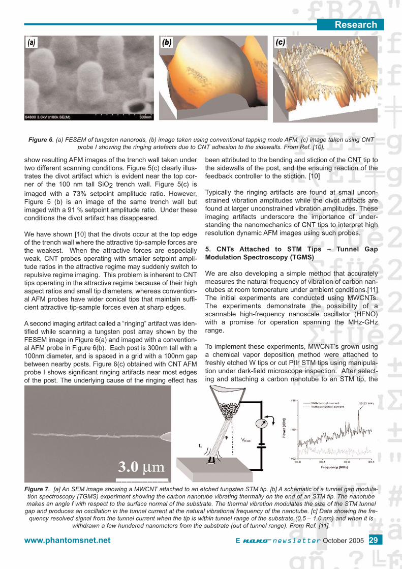
show resulting AFM images of the trench wall taken undertwo different scanning conditions. Figure 5(c) clearly illus-trates the divot artifact which is evident near the top cor-ner of the 100 nm tall SiO2 trench wall. Figure 5(c) isimaged with a 73% setpoint amplitude ratio. However,Figure 5 (b) is an image of the same trench wall butimaged with a 91 % setpoint amplitude ratio. Under theseconditions the divot artifact has disappeared.
We have shown [10] that the divots occur at the top edgeof the trench wall where the attractive tip-sample forces arethe weakest. When the attractive forces are especiallyweak, CNT probes operating with smaller setpoint ampli-tude ratios in the attractive regime may suddenly switch torepulsive regime imaging. This problem is inherent to CNTtips operating in the attractive regime because of their highaspect ratios and small tip diameters, whereas convention-al AFM probes have wider conical tips that maintain suffi-cient attractive tip-sample forces even at sharp edges.
A second imaging artifact called a “ringing” artifact was iden-tified while scanning a tungsten post array shown by theFESEM image in Figure 6(a) and imaged with a convention-al AFM probe in Figure 6(b). Each post is 300nm tall with a100nm diameter, and is spaced in a grid with a 100nm gapbetween nearby posts. Figure 6(c) obtained with CNT AFMprobe I shows significant ringing artifacts near most edgesof the post. The underlying cause of the ringing effect has
been attributed to the bending and stiction of the CNT tip tothe sidewalls of the post, and the ensuing reaction of thefeedback controller to the stiction. [10]
Typically the ringing artifacts are found at small uncon-strained vibration amplitudes while the divot artifacts arefound at larger unconstrained vibration amplitudes. Theseimaging artifacts underscore the importance of under-standing the nanomechanics of CNT tips to interpret highresolution dynamic AFM images using such probes.
5. CNTs Attached to STM Tips – Tunnel GapModulation Spectroscopy (TGMS)
We are also developing a simple method that accuratelymeasures the natural frequency of vibration of carbon nan-otubes at room temperature under ambient conditions.[11]The initial experiments are conducted using MWCNTs.The experiments demonstrate the possibility of ascannable high-frequency nanoscale oscillator (HFNO)with a promise for operation spanning the MHz-GHzrange.
To implement these experiments, MWCNT’s grown usinga chemical vapor deposition method were attached tofreshly etched W tips or cut PtIr STM tips using manipula-tion under dark-field microscope inspection. After select-ing and attaching a carbon nanotube to an STM tip, the
www.phantomsnet.net E newsletter October 2005 29
Figure 6. (a) FESEM of tungsten nanorods, (b) image taken using conventional tapping mode AFM, (c) image taken using CNTprobe I showing the ringing artefacts due to CNT adhesion to the sidewalls. From Ref. [10].
Figure 7. [a] An SEM image showing a MWCNT attached to an etched tungsten STM tip. [b] A schematic of a tunnel gap modula-tion spectroscopy (TGMS) experiment showing the carbon nanotube vibrating thermally on the end of an STM tip. The nanotubemakes an angle f with respect to the surface normal of the substrate. The thermal vibration modulates the size of the STM tunnel
gap and produces an oscillation in the tunnel current at the natural vibrational frequency of the nanotube. [c] Data showing the fre-quency resolved signal from the tunnel current when the tip is within tunnel range of the substrate (0.5 – 1.0 nm) and when it is
withdrawn a few hundered nanometers from the substrate (out of tunnel range). From Ref. [11].
Research

carbon nanotube/tip assembly was mounted in an STMoperating under ambient conditions. The STM head wasmounted on a two-stage vibration isolation system whichis enclosed by a carefully constructed Faraday cage.When the apex of the MWCNT is within tunnel range ofthe substrate, thermal vibrations of the MWCNT at its nat-ural resonance frequency modulate the tunnel gap to pro-duce a small but measurable contribution in the STM tun-nel current at a frequency determined by the resonant fre-quency of the MWCNT.
To measure the high frequency contribution of the tunnelcurrent, the high-gain preamplifier circuit for the STM wasmodified to allow for amplification and extraction of the RFsignal while allowing the required feedback control to oper-ate unimpeded. This is similar to the technique used inelectron spin resonance detection with STM. A commercialfrequency analyzer was used to measure the spectral con-tent from the RF amplifier. This instrument, while currentlylimited to frequencies lower than 40 MHz, allowed signalaveraging to further improve the signal to noise ratio.
Initial experiments focused on a comparison of frequencyspectra between clean PtIr tips and W tips with and withouta carbon nanotube attached. Spectral data were acquiredby placing the MWCNT tip in feedback mode above a fresh-ly cleaved HOPG substrate while using the spectrum ana-lyzer to measure the spectral content of the tunnel current.With proper attention to the setpoint conditions, we foundthat a reasonably stable tunnel current could be maintainedfor a few hours without noticeable degradation of the car-bon nanotube tip. Studies showed that current instabilities(momentary jump-to-contact events) tended to be moreprevalent for tunnel currents near 5 nA, presumably due toinstabilities in the tunnel gap. These variations gave rise tospectral components in the kHz range, well below the MHzfrequencies of interest here. For these reasons, tunnel cur-rents near 1 nA were typically used during data acquisitionin subsequent experiments.
A comparison of the spectral content of the output from theRF preamp (see Figure 7) showed clear evidence for thepresence of an additional spectral peak in the MHz rangewhen the MWCNT was in tunnelling range. Repeatedspectral scans provided convincing evidence for the exis-tence of a peak at a well-defined frequency. Parallel TEMstudies to measure the dimensions of the MWCNTshowed that the observed frequency peak could be rea-sonably explained by a simple model for a vibrating beamclamped at one end.
While these experiments are in their early stages, thepresence of a clear, repeatable and identifiable signal at awell defined frequency when the MWCNT tip was in tun-nel range provides convincing evidence that the observedspectral line is directly associated with the existence of ahigh frequency tunnel current produced at the tip of thecarbon nanotube.
6. Conclusions
A variety of experiments have been briefly reviewed whichillustrate the unique properties that result when a carbonnanotube is attached to either an STM or AFM tip. Bothsingle wall and multi walled carbon nanotubes have beenutilized. In most cases, the manipulation and successfulattachment of the nanotube to either STM or AFM tips wasachieved using a dark field microscope combined withmicromanipulators, equipment commonly available inmany laboratories. The experiments performed haveinvestigated such diverse properties of carbon nanotubesas electron emission, bending, vibration and SPM imagingartifacts.
This work has been supported in part by grants from theUS National Science Foundation (NSF) and the USNational Aeronautical and Space Administration (NASA).
7. References
[1] DE PABLO, P.J., GRAUGNARD, E., WALSH, B., ANDRES,P.J., DATTA, S., AND REIFENBERGER, R., A simple, reliabletechnique for making electrical contact to multi-walled carbonnanotubes, Appl. Phys. Lett. 74, 323-25 (1999). [2] GRAUGNARD, E., REIFENBERGER, R., WLASH, B., DEPABLO, P.J., Electronic Conductance of Multi-Walled CarbonNanotubes Having Reliable Electrical Contacts, in Cluster andNanostructure Interfaces, eds. P. Jena, S.N. Khanna, and B.K.Rao, World Scientific (Singapore), p. 123-30 (1999).[3] GRAGNARD, E. DE PABLO, P.J., WALSH, B., GHOSH, A.W.,DATTA, S., AND REIFENBERGER, R., TemperatureDependence of the conductance of multi-walled carbon nan-otubes, Phys. Rev. B64, 125407-414 (2001).[4] LEE, H.W., KIM, S.H. KWAK, Y.K., HAN, C.S., Nanoscale fab-rication of a single multi-walled carbon nanotube attached atom-ic force microscope tip using an electric field, Rev. Sci. Instrum.76, 046108-13 (2005).[5] STEVENS, R., NGUYEN, C., CASSELL, A., DELZEIT, L.,MEYYAPPAN, M., AND HAN, Improved fabrication approach forcarbon nanotube devices, Appl. Phys. Lett. 77, 3453-5 (2000).[6] LOVALL, D., BUSS M., ANDRES, R.P., ANDREIFENBERGER, R., Electron Emission and StructuralCharacterization of a Rope of Single Walled Carbon Nanotubes,Phys. Rev. B61, 5683-91 (2000).[7] LEE, S.I., HOWELL, S.W., RAMAN, A., REIFENBERGER, R.,NGUYEN, C.V., MEYYAPPAN, M., Nonlinear Tapping Dynamicsof Multi-Walled Carbon Nanotube Tipped Atomic ForceMicrocantilevers, Nanotechnology 15, 416-21 (2004).[8] LEE, S.I., HOWELL, S.W., RAMAN, A., REIFENBERGER, R.,NGUYEN, C.V., MEYYAPPAN, M., Complex Dynamics ofCarbon Nanotube Probe Tips, Ultramicroscopy 103, 95-102(2005).[9] SHARROS, B., RAMAN, R., REIFENBERGER, R., CoupledResonances and Mass Sensitivity of Carbon NanotubesSuspended from Silicon Microcantilevers (submitted).[10] STRUS, M., RAMAN, A., NGUYEN, C.V., HAN C.S.,Imaging Artefacts in Atomic Force Microscopy with CarbonNanotube Tips, Nanotechnology 16, 2482-92 (2005).[11] THERRIEN, J., LAN, C. AND REIFENBERGER, R., TunnelGap Modulation Spectroscopy, (submitted).
30 E newsletter October 2005 www.phantomsnet.net
Research

www.phantomsnet.net E newsletter October 2005 31
Advertisement