eecs 16a designing information devices and systems i midterm 2
TRANSCRIPT
1
EECS 16A Designing Information Devices and Systems ISpring 2021 Midterm 2
Midterm 2 Solution
1. HONOR CODEIf you have not already done so, please copy the following statements into the box provided for the honorcode on your answer sheet, and sign your name.
I will respect my classmates and the integrity of this exam by following this honor code. I affirm:
• I have read the instructions for this exam. I understand them and will follow them.
• All of the work submitted here is my original work.
• I did not reference any sources other than my two reference cheat sheets.
• I did not collaborate with any other human being on this exam.
2. (a) What other courses are you taking this semester? All answers will be awarded full credit; you canbe brief. (2 points)
(b) What has been your favorite part of 16A so far? All answers will be awarded full credit; you canbe brief. (2 points)
EECS 16A, Spring 2021, Midterm 2 1
2
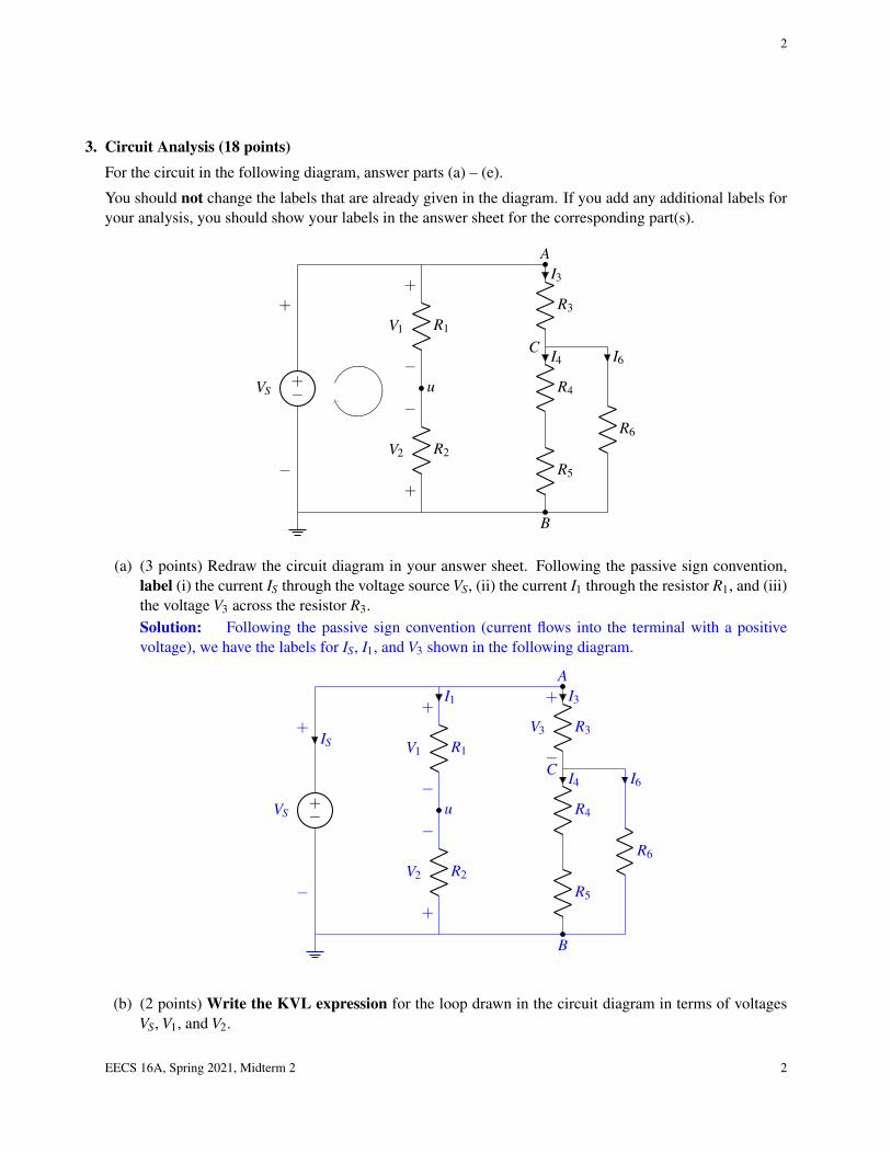
3. Circuit Analysis (18 points)For the circuit in the following diagram, answer parts (a) – (e).
You should not change the labels that are already given in the diagram. If you add any additional labels foryour analysis, you should show your labels in the answer sheet for the corresponding part(s).
−+VS
R2
+
−
V2
u
R1
−
+
V1
−
+
B
R5
R4
C
R3
AI3
I4 I6
R6
(a) (3 points) Redraw the circuit diagram in your answer sheet. Following the passive sign convention,label (i) the current IS through the voltage source VS, (ii) the current I1 through the resistor R1, and (iii)the voltage V3 across the resistor R3.Solution: Following the passive sign convention (current flows into the terminal with a positivevoltage), we have the labels for IS, I1, and V3 shown in the following diagram.
−+VS
IS
R2
+
−
V2
u
R1
−
+
V1
−
+
B
R5
R4
C
R3
−
+
V3
AI1 I3
I4 I6
R6
(b) (2 points) Write the KVL expression for the loop drawn in the circuit diagram in terms of voltagesVS, V1, and V2.
EECS 16A, Spring 2021, Midterm 2 2

3
Solution: If we travel in the loop, we will first meet the negative terminal of VS, the positive terminalof V1, and the negative terminal of V2, respectively. So the KVL expression is
−VS +V1−V2 = 0.
Any equivalent expressions (for example, VS−V1 +V2 = 0, VS +V2 =V1, etc.) are acceptable.
(c) (2 points) Write the KCL expression at node C in terms of currents I3, I4, and I6 as labeled in thecircuit diagram.Solution: I3 flows into the node, and I4, I6 flow out of the node, so the KCL expression is
−I3 + I4 + I6 = 0.
Any equivalent expressions (for example, I3− I4− I6 = 0, I3 = I4 + I6, etc.) are acceptable.
(d) (5 points) Given VS = 5 V, R1 = 1 kΩ, R2 = 4 kΩ, R3 = 2.5 kΩ, R4 = 1 kΩ, R5 = 4 kΩ, R6 = 5 kΩ,solve for the values of the element voltages V1, V2, and the node voltage u. Show your work. Youcan use any circuit analysis techniques you have learned in this course.Solution: We can solve this problem by NVA. Based on our labels in part (a), further label the currentthrough R2:
−+VS
IS
R2
+
−
V2
u
R1
−
+
V1
−
+
B
R5
R4
C
R3
−
+
V3
AI1
I2
I3
I4 I6
R6
Write the KCL expression for the node with unknown voltage u:
I1 + I2 = 0.
Connect the node voltages with the element voltages:
V1 =VS−u,
V2 = 0−u =−u.
According to Ohm’s Law, we know
I1 =V1
R1=
VS−uR1
,
I2 =V2
R2=−uR2
.
EECS 16A, Spring 2021, Midterm 2 3

4
Plug in the KCL expression:
VS−uR1
+−uR2
= 0
⇒R1 +R2
R1R2u =
VS
R1
⇒u =R2
R1 +R2VS =
4 kΩ
1 kΩ+4 kΩ×5 V = 4 V.
Therefore,
V1 =VS−u = 5 V−4 V = 1 V,
V2 =−u =−4 V.
Alternative solution: We know R1 and R2 form a voltage divider for VS. From the voltage dividerequation we learned from the lecture, the node voltage
u =R2
R1 +R2VS =
4 kΩ
1 kΩ+4 kΩ×5 V = 4 V.
Therefore,
V1 =VS−u = 5 V−4 V = 1 V,
V2 =−u =−4 V.
(e) (6 points) Given VS = 5 V, R1 = 1 kΩ, R2 = 4 kΩ, R3 = 2.5 kΩ, R4 = 1 kΩ, R5 = 4 kΩ, R6 = 5 kΩ.
i. If we combine R3, R4, R5, and R6 as an equivalent resistor Req connecting between the nodesA and B, what is the value of Req?
ii. What are the values of the current I3 and the power dissipated by R3? Show your work.
Solution: Between nodes C and B, we have R4 and R5 in series, and their equivalent resistor is inparallel with R6, so the equivalent resistance for R4, R5, and R6 between nodes C and B is
Req,C−B =(R4 +R5)R6
(R4 +R5)+R6=
(1 kΩ+4 kΩ)×5 kΩ
1 kΩ+4 kΩ+5 kΩ= 2.5 kΩ.
Req,C−B is in series with R3, so
Req = Req,C−B +R3 = 2.5 kΩ+2.5 kΩ = 5 kΩ.
The current I3 is the same as the current through Req if we replace R3, R4, R5, and R6 with Req, i.e.
I3 =VS
Req=
5 V5 kΩ
= 1 mA.
Therefore, the power dissipated by R3 is
PR3 = I32R3 = (1 mA)2×2.5 kΩ = 2.5 mW.
EECS 16A, Spring 2021, Midterm 2 4

5
4. Capacitive TouchSki (12 points)
One of your friendly lab TAs is preparing to go skiing for the first time! As excited as she is, she’s veryworried about losing her balance. To ease her mind, she decides to apply what she knows about capacitorsto create a circuit that will indicate if there is excessive force applied to either ski.
In this question, we will examine a force-sensing circuit for a single ski.
(a) (3 points) To create a sufficiently large capacitance, your TA affixes conductive plates to both thebottom of the boot and the top of the ski, with a thin insulating layer with permittivity ε in between.The boot has area Aboot and overlaps completely with the ski. Measurements show that the thicknesst of the insulating layer varies with the force F as t = 1
kF , where k is some constant. Write thecapacitance Cboot as a function of the force applied, the area of the boot, and constants.Solution:
Cboot = εAboot
t= εAbootkF
(b) (4 points) In order to measure the capacitance Cboot, you are given the following circuit. Assume thecapacitors have no initial charge before connected to the voltage source.
−+Vs
Cboot
Cfixed
+
−
Vboot
What is the voltage Vboot in terms of Vs, Cboot, and Cfixed?Solution:
Vboot =Cfixed
Cboot +CfixedVs
(c) (5 points) Now, you’d like to control an LED based on the force applied to the ski. Redraw thefollowing circuit in your answer sheet, complete the circuit so it sets Vout = 5V when Vboot < 2.5V,and Vout = 0V when Vboot > 2.5V (you don’t need to consider the special case when Vboot = 2.5V).You may use one comparator and up to two additional voltage sources.
EECS 16A, Spring 2021, Midterm 2 5

6
−+5 V
Cboot
Cfixed
+
−
Vboot
Vout
Rlim
LED
Solution:
−+5 V
Cboot
Vboot
Cfixed
−
+
−+2.5V
Vout
Rlim
LED
−+
5V
Note that the node Vboot should be connected to the negative terminal of the comparator, and the otherend of Cboot should be grounded. The power rails VDD = 5 V and VSS = 0 V should be specified in youranswer, however we will grant full credit if you label the correct VDD and VSS values without drawingthe 5 V voltage source for VDD.
EECS 16A, Spring 2021, Midterm 2 6

7
5. Resistive Temperature Sensor (17 points)
Oh no! Predictably, your lab TA gets hurt on the first day of her ski trip and is instructed to ice her injuryregularly. However, she’s finding that the ice packs are often too cold or too warm and needs a way to tracktheir temperature.
Fortunately, she remembers from 16A that the resistance of many resistors is dependent on temperature!Using this information, you decide to help her build a temperature-sensing device.Note: in this problem, temperature T is measured in the unit of Celsius.
(a) (6 points) You have different types of resistive bars available in your lab. For each of the followingtwo resistive bars, express the total resistance in terms of the given quantities and dimensions.
resistivity of copper = ρCo(1+αT ) Ω · cmresistivity of nickel = ρNo(1+βT ) Ω · cm
i.
CopperNickel
5 cm5 cm
I
2 cm
2cm
ii.
Copper
Nickel
10 cm
I
1 cm
1 cm
1 cm
Solution:i. For this bar, RTotal = RCopper +RNickel
RCopper = ρCLA=
54
ρCo(1+αT )
RNickel = ρNLA=
54
ρNo(1+βT )
RTotal =54(ρCo(1+αT )+ρNo(1+βT ))
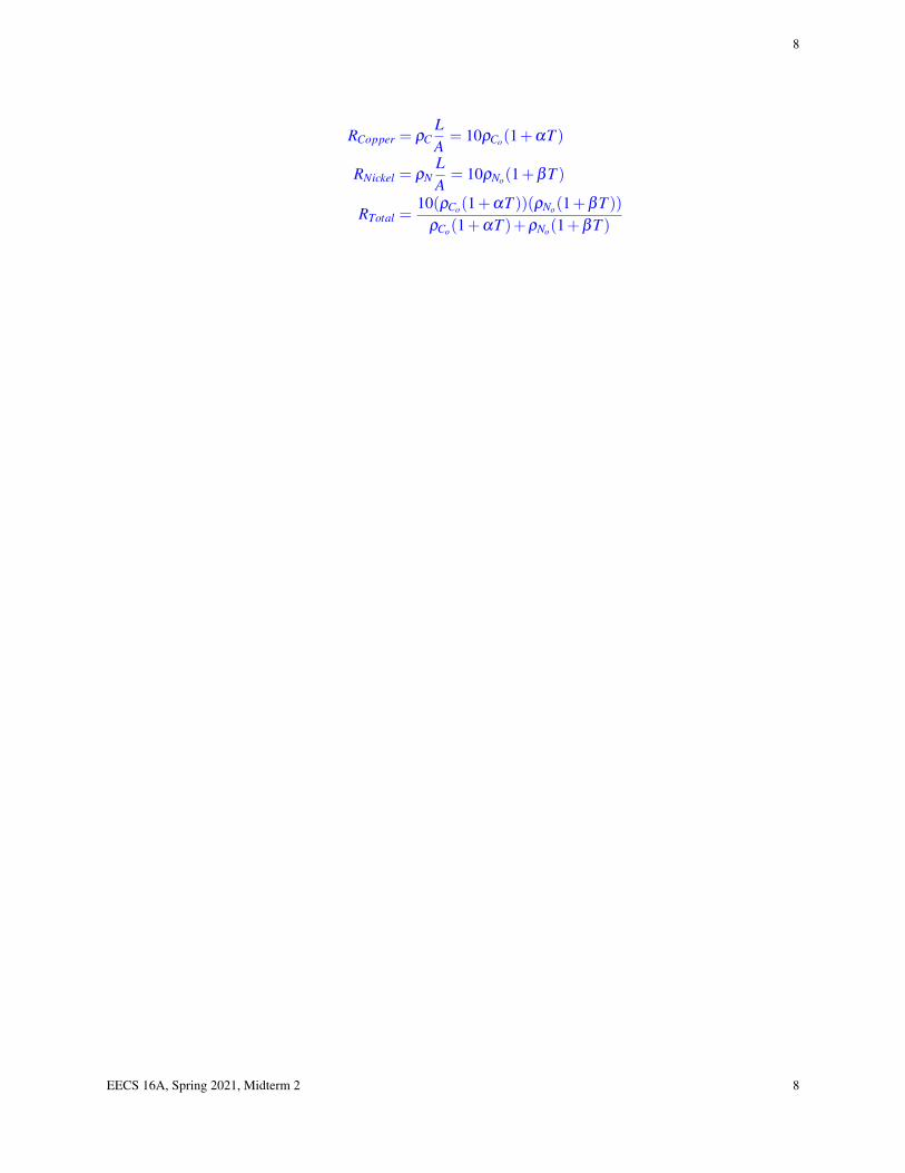
ii. For this bar, RTotal = RCopperRNickelRCopper+RNickel
EECS 16A, Spring 2021, Midterm 2 7
8
RCopper = ρCLA= 10ρCo(1+αT )
RNickel = ρNLA= 10ρNo(1+βT )
RTotal =10(ρCo(1+αT ))(ρNo(1+βT ))
ρCo(1+αT )+ρNo(1+βT )
EECS 16A, Spring 2021, Midterm 2 8

9
(b) (5 points) You have the following circuit that has a temperature dependent resistive bar RT and a resis-tor with fixed resistance R f . For this part only, assume Vs = 5 V, R f = 4 kΩ, and RT has resistivityρT = 100(1+0.01T ) Ω · cm and cross-sectional area A = 1 cm2.
−+Vs
RT
R f
+
−
Vmeas
Figure 5.1: Circuit diagram for parts (b) and (c).
You want to be able to measure temperature T within the range −10°C ≤ T ≤ 30°C. You also want tolimit the current flow through the resistive bar to be no more than 1 mA. Find the minimum length ofthe resistive bar RT such that the current limit is met for all temperatures in the specified range.Solution: Since Vs = 5 V, to have a maximum current of 1 mA, the minimum total resistance shouldbe 5 kΩ.The total resistance in this circuit is R f +ρT
LA = R f +100(1+0.01T ) L
A , which increases with temper-ature, so the lowest total resistance occurs when the temperature is −10°C. Therefore,
RTotal ≥ R f +100(1+0.01×−10)LA= 4 kΩ+90 Ω · cm
L1 cm2 ≥ 5 kΩ
L≥ 100090
cm
Lmin =100
9cm≈ 11.1 cm
(c) (6 points) Next, you are tasked with measuring the voltage across RT .
i. Draw how you would attach an ideal voltmeter to the circuit in Figure 5.1, in order to mea-sure the voltage across RT .
ii. Instead of an ideal voltmeter, you only have a practical voltmeter that can be modeled as an idealvoltmeter coming with a parallel internal resistance Rint , shown below. You connect the practicalvoltmeter to the same two nodes where you would attach the ideal voltmeter. Assuming RT =1000 Ω for this part, determine the minimum value of Rint such that the equivalent resistanceacross the voltmeter is no less than 99% of RT .
EECS 16A, Spring 2021, Midterm 2 9

10
Rint V
a
b
Solution: Attach an ideal voltmeter:
−+Vs
R f ixed
RT V
+
−
vmeas
For a practical voltmeter, the equivalent circuit is:
−+Vs
R f ixed
RT Rint V
+
−
vmeas
We find Req and set it to be equal to 0.99RT .
Req =RT Rint
RT +Rint
0.99RT (RT +Rint) = RT Rint
0.99(RT +Rint) = Rint
Rint =0.99RT
0.01Rint = 99000 Ω = 99 kΩ
EECS 16A, Spring 2021, Midterm 2 10

11
6. Data Conversion Circuits (22 points)
(a) (4 points) Photonic circuits use light to communicate. We still need to convert the light into electricityby a photodiode to process it. We can model the photodiode as a current source Is. Sometimes it isnecessary at the receiver side to adjust the transmitted voltage level Vout , and one way to do this isusing a voltage source Vbias. Consider this simple photonic receiver circuit:
Is
Rs
Rb
−+ Vbias
Vout
Using superposition, solve for the voltage Vout in terms of Is, Vbias, Rs, and Rb. Show your work.Solution: First turn off the current source and turn on the voltage source. The circuit is an opencircuit now, so Vout,1 = Vbias. Then turn off the voltage source and turn on the current source, thecurrent in the circuit is Is, so Vout,2 = IsRb. By superposition, Vout =Vout,1 +Vout,2 =Vbias + IsRb.
(b) (4 points) The previous receiver circuit may have problems with loading. Instead, we may use anop-amp, such as in this circuit:
−
+
−+ Vbias
Is
R
Vout
Calculate the voltage at the output Vout in terms of Is, Vbias, and R. Show your work. You will notreceive full credit for directly copying a formula from your cheat sheet.Solution: All the current Is goes through the resistor, so the voltage drop on the resistor is VR =−IsR.From our golden rules, the voltage of the negative terminal of the op-amp must be Vbias. Therefore,
Vout =Vbias +VR =Vbias− IsR
EECS 16A, Spring 2021, Midterm 2 11

12
(c) (4 points) We need some circuits to convert between our analog voltage values and some digital repre-sentation stored in 1s and 0s. We mentioned digital-to-analog converter circuits, or DACs, in lecture.Let’s inspect one here:
R
R
R
R
−+ VDD
0
1
N−3
N−2
N−1
−
Vout
+
Note that there are N resistors and N switches in the circuit. Depending on some input digital code,one of the switches is closed, connecting the output to some node in the resistor ladder.If only the ith switch is closed (0≤ i≤ N−1), what is the output voltage Vout in terms of VDD, i, N,and R?Solution: This is similar to our touchscreen problem. We can divide the resistor ladder into a topand bottom, then count up the number of resistors we have that form the top and bottom.
Vout =Rbot
Rtop +RbotVDD
=iR
iR+(N− i)RVDD
=iN
VDD
EECS 16A, Spring 2021, Midterm 2 12

13
(d) (4 points) The dual to DAC circuits are analog-to-digital converters, or ADC circuits. Here is anexample of one, using resistors and comparators:
R
R
R
R
−+ VDD
−
+b0
−
+b1
−
+b2
−+Vin
Note: The red wires in the diagram are regular wires, but have been colored to show that they do nottouch the crossing black wires.The resistor ladder gives us a set of reference voltages to compare against. We use a set of comparatorsto compare the input voltage Vin against these reference levels, and we get out a corresponding digitalcode b0, b1, and b2.Assume that VDD = 1V, and that the comparators are connected to rails VDD = 1V and VSS = 0V. IfVin is 0.3V, what are the outputs b0, b1, and b2?Solution: The reference voltages for the comparators, from bottom to top, are 1
4VDD = 0.25 V,12VDD = 0.5 V, and 3
4VDD = 0.75 V. Each comparator checks if Vin is greater than the reference voltage,outputing VDD if it is greater and VSS if not. We are given Vin = 0.3 V, so b0 =VDD = 1V, b1 =VSS = 0V,b2 =VSS = 0V.If you left your answer in terms of 1s and 0s, i.e. b0 = 1,b1 = 0,b2 = 0, we will accept that for fullcredit.
EECS 16A, Spring 2021, Midterm 2 13

14
(e) (6 points) These DAC and ADC circuits help us represent numbers using voltage values. We wouldlike to build some blocks that let us compute, e.g. add and multiply, with these numbers. We call this"analog computing," and we saw an example of this previously in the "artificial neuron" circuit. Theseanalog compute circuits have potentially massive speed benefits over comparable digital compute cir-cuits. (Take EECS151 and EE140 for more details).
DAC
DAC
Compute ADC
Consider one such compute circuit below, the differential amplifier. This is a common circuit in audioamplifiers but is also a useful tool for mathematical computing. Find the output Vout in terms of V1,V2, R1, and R2.
−
+R1
R2
R1
R2
VoutV1
V2
Solution: Let’s approach this problem with superposition. First we turn off V2 and keep V1 on. Notethat we have no current flowing through the resistors at the positive terminal, so we effectively haveground at that node. Thus, this is just an inverting amplifier:
Vout =−R2
R1V1
Next, we turn off V1 and keep V2 on. We have two things happening in this circuit. The first pair R1and R2 connecting V2 to the positive terminal form a resistive voltage divider. Then the op-amp andthe feedback R1 and R2 form a non-inverting amplifier:
Vout =R2
R1 +R2
R1 +R2
R1V2 =
R2
R1V2.
Adding these together, we get:
Vout =−R2
R1V1 +
R2
R1V2 =
R2
R1(V2−V1)
EECS 16A, Spring 2021, Midterm 2 14

15
7. Aid to the Resistance (13 points)
The main ship of the Resistance Fleet is in trouble! They have recruited you to help fix the issue. Theon-board technicians have determined that the resistor grid in the main console is faulty (one of the resistorsmust be fried). It is your job to replace the grid with something of equivalent resistance. However, becauseof severe budget cuts in the Resistance’s EE department, you can only use a single resistor connectedbetween nodes A and B to replace the resistor grid. The technicians hand you the diagram below of whatthe resistor grid looked like. All resistors in the diagram have resistance value R.
A
B
repeating forever ->
(a) (5 points) Find the equivalent resistance of the following piece of the resistor grid between nodes Aand B in terms of R.Hint: If a resistor has no current flowing through it, what is it equivalent to?
A
B
Solution: By symmetry, we can argue that the voltage across the horizontal resistor is 0, i.e. there isno current flowing through the horizontal resistor (recall our resistor grid model for the resistive touchscreen). Because of this, we can model the horizontal resistor as an open circuit without changing thebehavior of the resistor grid, giving us the equivalent circuit below:
EECS 16A, Spring 2021, Midterm 2 15

16
A
B
The equivalent resistance of this portion is:
Req =(2R)(2R)2R+2R
= R.
EECS 16A, Spring 2021, Midterm 2 16

17
(b) (5 points) Find the equivalent resistance of the following piece of the resistor grid between nodes Aand B in terms of R.Hint: (i) Because the pattern is infinite, the equivalent resistance of the circuit in the red box and theequivalent resistance of the circuit in the blue box are equal.(ii) The solutions to the quadratic equation ax2 +bx+ c = 0 are −b±
√b2−4ac
2a .
A
B
repeating forever ->
Solution: The hint points us to the below equivalent circuit:
A R
B RR Req
We can now set up an equation for Req in terms of itself:
Req = R+R||Req +R
Req = 2R+RReq
R+Req
Req−2R =RReq
R+Req
RReq = (Req−2R)(R+Req)
0 = R2eq−2RReq−2R2
Req =2R±
√4R2 +8R2
2
Req =2R±
√12R2
2Req = R±
√3R
Req = (1+√
3)R
Notice that we took the positive solution because resistance cannot be negative.
(c) (3 points) Suppose the equivalent resistance for the piece of resistor grid in part (a) is αR, and theequivalent resistance for the piece of resistor grid in part (b) is βR, where α and β are known real
EECS 16A, Spring 2021, Midterm 2 17

18
numbers for this part. What should be the value of the resistor you use to replace the entire gridwith, in terms of R, α , and β?Solution: The pieces we see above are put in parallel in the final resistor grid, making the equivalentresistance of the entire grid:
R f =ReqaReqb
Reqa +Reqb
=αβ
α +βR
In order to replace the resistor grid, we would need to purchase a resistor of resistance R f , as specifiedabove.
EECS 16A, Spring 2021, Midterm 2 18
19
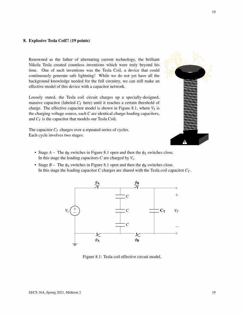
8. Explosive Tesla Coil!! (19 points)
Renowned as the father of alternating current technology, the brilliantNikola Tesla created countless inventions which were truly beyond histime. One of such inventions was the Tesla Coil, a device that couldcontinuously generate safe lightning! While we do not yet have all thebackground knowledge needed for the full circuitry, we can still make aneffective model of this device with a capacitor network.
Loosely stated, the Tesla coil circuit charges up a specially-designed,massive capacitor (labeled CT here) until it reaches a certain threshold ofcharge. The effective capacitor model is shown in Figure 8.1, where VS isthe charging voltage source, each C are identical charge-loading capacitors,and CT is the capacitor that models our Tesla Coil.
The capacitor CT charges over a repeated series of cycles.Each cycle involves two stages:
• Stage A – The φB switches in Figure 8.1 open and then the φA switches close.In this stage the loading capacitors C are charged by Vs.
• Stage B – The φA switches in Figure 8.1 open and then the φB switches close.In this stage the loading capacitor C charges are shared with the Tesla coil capacitor CT .
−+Vs
φA
C
C
C
φA
φB
CT
φB
+
−
VT
Figure 8.1: Tesla coil effective circuit model.
EECS 16A, Spring 2021, Midterm 2 19
20
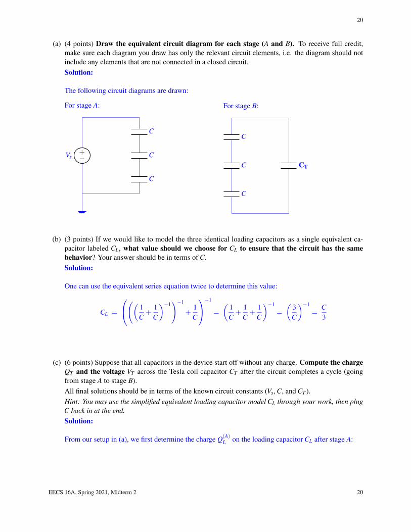
(a) (4 points) Draw the equivalent circuit diagram for each stage (A and B). To receive full credit,make sure each diagram you draw has only the relevant circuit elements, i.e. the diagram should notinclude any elements that are not connected in a closed circuit.Solution:
The following circuit diagrams are drawn:
For stage A:
−+Vs
C
C
C
For stage B:
C
C
C
CT
(b) (3 points) If we would like to model the three identical loading capacitors as a single equivalent ca-pacitor labeled CL, what value should we choose for CL to ensure that the circuit has the samebehavior? Your answer should be in terms of C.Solution:
One can use the equivalent series equation twice to determine this value:
CL =
(( 1C+
1C
)−1)−1
+1C
−1
=
(1C+
1C+
1C
)−1
=
(3C
)−1
=C3
(c) (6 points) Suppose that all capacitors in the device start off without any charge. Compute the chargeQT and the voltage VT across the Tesla coil capacitor CT after the circuit completes a cycle (goingfrom stage A to stage B).All final solutions should be in terms of the known circuit constants (Vs, C, and CT ).Hint: You may use the simplified equivalent loading capacitor model CL through your work, then plugC back in at the end.Solution:
From our setup in (a), we first determine the charge Q(A)L on the loading capacitor CL after stage A:
EECS 16A, Spring 2021, Midterm 2 20

21
−+Vs CL = 1
3C
Q(A)L = CL Vs =
13
C Vs
Next we transition to stage B and recognize that the total charge on the upper node is Q(A)L . From here
we can identify the voltage VT by assembling the equivalent capacitance that this charge resides on,which is just CL and CT in parallel.
CL = 13C CT
Ceq = CL +CT
Lastly we determine VT , and consequently QT :
VT =Q(A)
LCeq
= Vs
(C
C+3CT
)
QT = CT Vs
(C
C+3CT
)
(d) (6 points) Now suppose that the Tesla coil capacitor CT starts with an initial charge Q0, which wascollected as a result of previous cycles.
i. Compute the charge QT and the voltage VT across the Tesla coil capacitor CT after the circuitcompletes a cycle (going from stage A to stage B). For simplicity, you can assume the loadingcapacitors still start off without any charge.
ii. Compute the ratio σ of energy stored on CT before and after this cycle (so σ = Eafter/Ebefore).You can get partial credit for writing the expressions for Ebefore and Eafter.At which value of initial charge Q0 do we no longer add energy to the coil after a cycle?
All final solutions should be in terms of the known circuit constants (Vs, C, CT , and Q0).Hint: It may be helpful to simplify the final answer of σ in the form:
σ =
(3(CT
C
)+___
3(CT
C
)+___
)2
where the ___ spaces are yet to be discovered by you!
EECS 16A, Spring 2021, Midterm 2 21
22
Solution:
The work in computing Q(A)L from the previous subpart still holds. In fact, the only change in this
new scenario is that during φB the total charge being shared across CL and CT in parallel is nowQ(A)
L → Q(A)L +Q0. Thus we end up with:
VT =Q(A)
L +Q0
Ceq=
C Vs +3Q0
C+3CT= Vs
(C+(3Q0/Vs)
C+3CT
)
QT = CT Vs
(C+(3Q0/Vs)
C+3CT
)As expected, we should attain the same results as in the previous subpart for the special case thatQ0 = 0. Now we turn to compute the change in stored energy on CT using the formula Estored =
12CV 2 = 1
2Q2
C . In this context, our ratio becomes EafterEbefore
=(
QafterQbefore
)2, thus
σ =Eafter
Ebefore=
(CT Vs
C+(3Q0/Vs)C+3CT
Q0
)2
=
(3(CT
C
)+ CTVs
Q0
3(CT
C
)+1
)2
We are increasing the energy stored in the coil CT whenever σ > 1. Thus at the point σ = 1 is whenwe are maximally charged and do not increase the capacitor energy. From our expression, this occurswhen Q0 =CTVs. This is when the coil is charged to the supply voltage level VT =Vs.
EECS 16A, Spring 2021, Midterm 2 22