eindhoven university of technology master memory pattern ... fileembedded systems den dolech 2, 5600...
TRANSCRIPT

Eindhoven University of Technology
MASTER
Memory pattern generation based on specification and environment
Hayes Jr, W.S.
Award date:2009
Link to publication
DisclaimerThis document contains a student thesis (bachelor's or master's), as authored by a student at Eindhoven University of Technology. Studenttheses are made available in the TU/e repository upon obtaining the required degree. The grade received is not published on the documentas presented in the repository. The required complexity or quality of research of student theses may vary by program, and the requiredminimum study period may vary in duration.
General rightsCopyright and moral rights for the publications made accessible in the public portal are retained by the authors and/or other copyright ownersand it is a condition of accessing publications that users recognise and abide by the legal requirements associated with these rights.
• Users may download and print one copy of any publication from the public portal for the purpose of private study or research. • You may not further distribute the material or use it for any profit-making activity or commercial gain

Embedded Systems
Den Dolech 2,5600 MB Eindhoven
The Netherlandshttp://w3.win.tue.nl/en/
2009
MSc THESIS
Memory Pattern Generation based on
Specification and Environment
Williston Sterchi Hayes Jr.
Abstract
Faculty of Mathematics and Computer Science
ES-MS-2009-0614000
Guaranteeing hard real-time requirements in systems with multiplerequestors accessing a single memory is a difficult task due to vari-able access times of SDRAMs. This problem has been solved withthe use of the Predator memory controller, which is able to put abound on worst-case latency and worst-case bandwidth. This con-troller uses precomputed sequences of SDRAM commands, calledmemory access patterns, in order to interact with SDRAMs. How-ever, these patterns are difficult to construct due the complexity ofSDRAM timing parameters and constraints. Thus, three heuristic-based pattern generation algorithms are developed that explore thetrade-offs between run time and bandwidth offered. In the end, theapproach selected provides adequate bandwidth while still offering alow run time. This pattern generator has been integrated into thePredator memory controller design flow.


Memory Pattern Generation based on
Specification and Environment
THESIS
submitted in partial fulfillment of therequirements for the degree of
MASTER OF SCIENCE
in
EMBEDDED SYSTEMS
by
Williston Sterchi Hayes Jr.
born in San Francisco, The United States of America
Embedded SystemsDepartment of Computer Science and EngineeringFaculty of Mathematics and Computer ScienceEindhoven University of Technology


Memory Pattern Generation based on
Specification and Environment
by Williston Sterchi Hayes Jr.
Abstract
Guaranteeing hard real-time requirements in systems with multiple requestors accessing asingle memory is a difficult task due to variable access times of SDRAMs. This problem hasbeen solved with the use of the Predator memory controller, which is able to put a bound
on worst-case latency and worst-case bandwidth. This controller uses precomputed sequences ofSDRAM commands, called memory access patterns, in order to interact with SDRAMs. However,these patterns are difficult to construct due the complexity of SDRAM timing parameters andconstraints. Thus, three heuristic-based pattern generation algorithms are developed that explorethe trade-offs between run time and bandwidth offered. In the end, the approach selected providesadequate bandwidth while still offering a low run time. This pattern generator has been integratedinto the Predator memory controller design flow.
Laboratory : Embedded Systems
Committee Members :
Advisor: Henk Corporaal, Electronic Systems, TU\e
Member: Benny Akesson, Electronic Systems, TU\e
Member: Kees Goossens, SAI, NXP
i

ii

iii

iv

Contents
List of Figures viii
List of Tables ix
Acknowledgements xi
1 Introduction 1
1.1 Application Requirements . . . . . . . . . . . . . . . . . . . . . . . . . . . 1
1.2 Considered Systems - Platform . . . . . . . . . . . . . . . . . . . . . . . . 2
1.3 Problem Statement . . . . . . . . . . . . . . . . . . . . . . . . . . . . . . . 3
1.4 Goal . . . . . . . . . . . . . . . . . . . . . . . . . . . . . . . . . . . . . . . 4
1.5 Contributions . . . . . . . . . . . . . . . . . . . . . . . . . . . . . . . . . . 4
1.6 Outline . . . . . . . . . . . . . . . . . . . . . . . . . . . . . . . . . . . . . 4
2 SDRAM 7
2.1 Architecture . . . . . . . . . . . . . . . . . . . . . . . . . . . . . . . . . . . 7
2.2 Commands . . . . . . . . . . . . . . . . . . . . . . . . . . . . . . . . . . . 8
2.3 Timing Constraints . . . . . . . . . . . . . . . . . . . . . . . . . . . . . . . 10
3 Memory Efficiency 13
3.1 Peak Bandwidth . . . . . . . . . . . . . . . . . . . . . . . . . . . . . . . . 13
3.2 Data Efficiency . . . . . . . . . . . . . . . . . . . . . . . . . . . . . . . . . 13
3.3 Bank Efficiency . . . . . . . . . . . . . . . . . . . . . . . . . . . . . . . . . 14
3.4 Switching Efficiency . . . . . . . . . . . . . . . . . . . . . . . . . . . . . . 15
3.5 Refresh Efficiency . . . . . . . . . . . . . . . . . . . . . . . . . . . . . . . . 15
3.6 Net Bandwidth . . . . . . . . . . . . . . . . . . . . . . . . . . . . . . . . . 15
4 Memory Controllers 17
4.1 Arbiter . . . . . . . . . . . . . . . . . . . . . . . . . . . . . . . . . . . . . 17
4.2 Memory Mapping . . . . . . . . . . . . . . . . . . . . . . . . . . . . . . . . 18
4.3 Command Generator . . . . . . . . . . . . . . . . . . . . . . . . . . . . . . 21
4.4 Types of Memory Controllers . . . . . . . . . . . . . . . . . . . . . . . . . 21
5 Memory Patterns 25
5.1 Pattern Overview . . . . . . . . . . . . . . . . . . . . . . . . . . . . . . . . 25
5.2 Types of Patterns . . . . . . . . . . . . . . . . . . . . . . . . . . . . . . . . 26
5.3 Pattern Dominance . . . . . . . . . . . . . . . . . . . . . . . . . . . . . . . 27
5.4 Efficiency Calculations . . . . . . . . . . . . . . . . . . . . . . . . . . . . . 29
5.5 Latency Calculation . . . . . . . . . . . . . . . . . . . . . . . . . . . . . . 31
5.6 Optimality . . . . . . . . . . . . . . . . . . . . . . . . . . . . . . . . . . . 32
v

6 Algorithm Approaches 356.1 Pattern Generation Design Decisions . . . . . . . . . . . . . . . . . . . . . 356.2 Branch and Bound . . . . . . . . . . . . . . . . . . . . . . . . . . . . . . . 396.3 As Soon As Possible Scheduling . . . . . . . . . . . . . . . . . . . . . . . . 436.4 Bank Scheduling . . . . . . . . . . . . . . . . . . . . . . . . . . . . . . . . 456.5 Results . . . . . . . . . . . . . . . . . . . . . . . . . . . . . . . . . . . . . . 46
7 Algorithm Context 497.1 Tooling Flow Overview . . . . . . . . . . . . . . . . . . . . . . . . . . . . . 497.2 Integration of Pattern Generator . . . . . . . . . . . . . . . . . . . . . . . 517.3 Non-allocated Bandwidth Calculations . . . . . . . . . . . . . . . . . . . . 547.4 Experimental Results . . . . . . . . . . . . . . . . . . . . . . . . . . . . . . 55
8 Conclusion 61
9 Future Work 639.1 3D Stacking . . . . . . . . . . . . . . . . . . . . . . . . . . . . . . . . . . . 639.2 Optimal Pattern Generation . . . . . . . . . . . . . . . . . . . . . . . . . . 639.3 Low Power Considerations . . . . . . . . . . . . . . . . . . . . . . . . . . . 639.4 Future SDRAM Iterations . . . . . . . . . . . . . . . . . . . . . . . . . . . 64
Bibliography 65
A List of relevant DDR timing constraints and parameters 67
B Glossary 69
C Latency Equation Derivations 71
D Requestor Specification 73
E DDR Memory Specification 75
vi

List of Figures
1.1 General overview of the considered system. . . . . . . . . . . . . . . . . . 2
2.1 SDRAM Bank Architecture . . . . . . . . . . . . . . . . . . . . . . . . . . 8
2.2 SDRAM Activate and Precharge Loop. . . . . . . . . . . . . . . . . . . . . 9
2.3 Example of a command sequence. . . . . . . . . . . . . . . . . . . . . . . . 9
2.4 Example of tRRD , tRCD , BurstSize, and DataRate requirements andparameters. . . . . . . . . . . . . . . . . . . . . . . . . . . . . . . . . . . . 10
3.1 Visual representation of bank efficiency. Blank slots in the command busrepresent NOP commands. . . . . . . . . . . . . . . . . . . . . . . . . . . . 14
4.1 Architecture of a memory controller. . . . . . . . . . . . . . . . . . . . . . 17
4.2 Illustration of a continuous memory map. . . . . . . . . . . . . . . . . . . 18
4.3 Example of commands generated for a continuous memory map (top) andan interleaving map (bottom). The data bus has been wrapped back ontoitself. . . . . . . . . . . . . . . . . . . . . . . . . . . . . . . . . . . . . . . . 19
4.4 Illustration of an interleaving memory map . . . . . . . . . . . . . . . . . 20
4.5 Illustration of best-case scenario when using a continuous memory map(top) compared to an interleaving memory map (bottom) . . . . . . . . . 21
4.6 Illustration of worst-case scenario when using a continuous memory map(top) compared to an interleaving memory map (bottom) . . . . . . . . . 21
4.7 Illustration showing reordering of commands to reduce data bus directionchanges. The top figure shows the requests in order, the bottom figureshows the requests reordered. . . . . . . . . . . . . . . . . . . . . . . . . . 22
5.1 Sequence of various patterns. . . . . . . . . . . . . . . . . . . . . . . . . . 25
5.2 Read pattern for DDR2-400 SDRAM. Blank schedule slots indicate NOPcommands. . . . . . . . . . . . . . . . . . . . . . . . . . . . . . . . . . . . 26
5.3 Write pattern for DDR2-400 SDRAM. . . . . . . . . . . . . . . . . . . . . 26
5.4 Switching patterns being used between read and write patterns. . . . . . . 27
5.5 Illustration of read dominance. . . . . . . . . . . . . . . . . . . . . . . . . 27
5.6 Illustration of write dominance. . . . . . . . . . . . . . . . . . . . . . . . . 28
5.7 Illustration of mix dominance. . . . . . . . . . . . . . . . . . . . . . . . . . 28
5.8 Dominance scale viewed on a line. . . . . . . . . . . . . . . . . . . . . . . 29
6.1 Illustration of moving NOPs from back to front of pattern. . . . . . . . . 37
6.2 Example of command tree. . . . . . . . . . . . . . . . . . . . . . . . . . . 40
6.3 Flow diagram of the branch and bound algorithm. . . . . . . . . . . . . . 41
6.4 Pseudo-code of sanity check optimization. . . . . . . . . . . . . . . . . . . 42
6.5 Number of valid patterns at BurstCount 2 for a DDR2-400 SDRAM device 43
6.6 Pseudo-code of ASAP algorithm . . . . . . . . . . . . . . . . . . . . . . . 44
6.7 Flowchart of the ASAP algorithm . . . . . . . . . . . . . . . . . . . . . . . 44
vii

6.8 Example of a pattern generated by the ASAP algorithm (top), and apattern generated by the branch and bound algorithm (bottom). . . . . . 44
6.9 Pseudo-code of bank scheduling algorithm . . . . . . . . . . . . . . . . . . 456.10 Flow diagram of the bank scheduling algorithm . . . . . . . . . . . . . . . 466.11 Comparison of net bandwidth guaranteed by algorithms for a DDR2-400
SDRAM. . . . . . . . . . . . . . . . . . . . . . . . . . . . . . . . . . . . . 476.12 Comparison of net bandwidth guaranteed by algorithms for a DDR2-800
SDRAM. . . . . . . . . . . . . . . . . . . . . . . . . . . . . . . . . . . . . 476.13 Comparison of net bandwidth guaranteed by algorithms for a DDR3-800
SDRAM. . . . . . . . . . . . . . . . . . . . . . . . . . . . . . . . . . . . . 486.14 Comparison of net bandwidth guaranteed by algorithms for a DDR3-1600
SDRAM. . . . . . . . . . . . . . . . . . . . . . . . . . . . . . . . . . . . . 48
7.1 Pseudo-code of integrated pattern generator. . . . . . . . . . . . . . . . . 527.2 Trade-off between edata and ebank. . . . . . . . . . . . . . . . . . . . . . . . 537.3 Flow of integrated pattern generator . . . . . . . . . . . . . . . . . . . . . 537.4 Illustration of Predator architecture. . . . . . . . . . . . . . . . . . . . . . 547.5 Comparison of fixed BurstCount generator and an iterating generator with
large request size. The memory specification used is DDR2-400. . . . . . . 577.6 Comparison of fixed BurstCount generator and an iterating generator with
large request size. The memory specification used is DDR2-400. . . . . . . 577.7 Comparison of fixed BurstCount generator and an iterating generator with
small request size. The memory specification used is DDR2-400. . . . . . 587.8 Comparison of fixed BurstCount generator and an iterating generator with
small request size. The memory specification used is DDR2-400. . . . . . 587.9 Average bandwidth over time for a DDR2-400 device by simulation. . . . 597.10 Average bandwidth over time for a DDR2-800 device by simulation. . . . 597.11 Average bandwidth over time for a DDR3-800 device by simulation. . . . 607.12 Average bandwidth over time for a DDR3-1600 device by simulation. . . . 60
viii

List of Tables
2.1 Typical characteristics of a DDR SDRAM device. . . . . . . . . . . . . . . 82.2 Comparison of timing constraints in nanoseconds and clock cycles for two
SDRAM devices. . . . . . . . . . . . . . . . . . . . . . . . . . . . . . . . . 10
4.1 Comparison of characteristics of different memory controllers. . . . . . . . 23
7.1 Example of normalized bandwidth changing with BurstCount. . . . . . . 557.2 Values of load, request size, and latency requirement. . . . . . . . . . . . . 56
ix

x

Acknowledgements
This project has been offered through NXP Semiconductors with cooperation from theEindhoven University of Technology. I would like to thank Kees Goossens and BennyAkesson for allowing me to join their team in the System-On-Chip Architecture & In-frastructure group (SAI). I am very grateful to Benny Akesson for his excellent guidanceand help during the course of this project. Without him this project would not havebeen possible. I am also grateful to Kees Goossens as he provided a lot of insight intothe project that allowed me to continually gain a new outlook on the thesis.
I would also like to thank Henk Corporaal for his valuable remarks and considerationsmade on the project. He always provided an interesting perspective, and encouraged theproject’s movement.
Additionally, Ad Siereveld and Roelof Salters at NXP are held in gratitude for sharingtheir deep knowledge of SDRAMs and SDRAM controllers with me. The informationreceived from them helped clarify many problems I encountered in this project.
I would like to thank all of my colleagues at NXP for the various discussions we heldand coffees we drank. Matteo Scordino, Ulf Winberg, Frank Ophelders, Dongrui She,Getachew Teshome, Pim Ritzen, Anna Kosek, Tion Kusumo, Jing Jing, Fabio Pania,and Adriano Sanches, you made this a great experience for me.
Williston Sterchi Hayes Jr.Eindhoven, The NetherlandsAugust 31, 2009
xi

xii

Introduction 1In this thesis we present a problem in the domain of real-time embedded systems thatutilize SDRAM devices. In Section 1.1, we introduce requirements that applications withreal-time requirements running on System-on-Chips (SoCs) have. This will be followed bySection 1.2, where we discuss the platform considered for this thesis. Section 1.3 detailsthe problem of using SDRAM devices with the requirements specified in Section 1.1.Section 1.4 presents our solution to the problem. This is followed by sections detailingour contributions as well as the outline of this thesis.
1.1 Application Requirements
As transistors have gotten smaller due to advances in technology, now entire systemscan be implemented on a single chip [13]. These SoCs typically have multiple IP blocks,and the gain offered by using SoCs is that the interconnect distance between IP blocksis typically much smaller than that of a traditional system. These shorter interconnectsreduce time needed to transfer information from one IP block to another. Additionally,these systems use less power, which is also of great importance to embedded systemsas power is a limited resource. We will now discuss the requirements of applicationsrunning on SoCs.
Applications running on real-time systems are used in a variety of situations, witheach situation requiring different behavior. The first type of application requirements issoft requirements, meaning that if a deadline is not met, there still might be some usefulinformation to be gained [5]. An example of an application with soft real-time require-ments is an MPEG-2 decoder. This type of application would require good average-casebandwidth. If frames are not fully processed in time then the picture may appear pix-ilated or blocky. Yet, one can imagine that a viewer would still prefer to see a blurrypicture over no picture at all.
The second type of requirements is hard-real time requirements. Applications whichhave hard real-time requirements cannot miss their deadlines under any circumstances[10,16]. An example of a system with hard real-time requirements is an anti-lock brakingsystem found in automobiles. These systems require a low worst-case latency. If thislatency requirement is not met, then the automobile’s wheels may lock up resulting inskidding, and loss of control of the vehicle.
Another aspect of applications running on SoCs is their latency requirements. Someapplications have very tight latency deadlines that must be respected, while other typesof applications have more lenient deadlines. Both must be accounted for.
In this thesis we focus on applications which have hard real-time requirements. Addi-tionally, we assume that we know nothing about the traffic that is generated, except forbandwidth and latency requirements. Finally, we state that we want to give guarantees
1

2 CHAPTER 1. INTRODUCTION
on worst-case latency and worst-case bandwidth that are analytically provable.
1.2 Considered Systems - Platform
This section details the system that is modeled. We have chosen to represent our systemas multiple processing elements utilizing a single memory controller. We define therequesting service from these processing elements to the memory controller as requestors.We consider the case where the memory controller is controlling a DDR-SDRAM [2]. Theentire overview can be seen in Figure 1.1.
The reason we represent our system as multiple processing elements using a singlememory controller is because this is often required in practical cases. Having multiplememories is not a cost effective way to store data, because it increases power consumptionand may require more expensive packaging. Thus, sharing memory decreases chip realestate and power usage, and results in a low cost-per-bit.
Memory ControllerNetworkOnChip
Processing
Processing
Processing
Element 1
Element 2
Element 3
DDR−SDRAM
Figure 1.1: General overview of the considered system.
1.2.1 Predictability
All SDRAMs are predictable in the sense that they have ranges of times in which datais accessed, however, these ranges are not indicative of normal performance. We hopeto place bounds on bandwidth and latency such that we can prove the exact value andmake the value useful, i.e. the bounds we place are improved over the absolute worst-case values listed in the specification. The reason why we are concerned about improvingworst-case values is that bandwidth is a shared, scarce resource, and has been proven tobe a main bottleneck in SoCs [6,12]. Thus, any improvement that can be determined inthe worst-case is very useful.
Definition 1.1 (Predictability) A predictable resource is one that has a known, use-
ful, worst-case bound.
The way a controller interacts with an SDRAM is by sending commands. Thesecommands take the form of a read command, a write command, and a few other auxiliarycommands. These read and write commands return a few words of data, the amount ofwhich depends on a memory parameter.

1.3. PROBLEM STATEMENT 3
The reason that placing bounds on latency and bandwidth is difficult is due to thefact that SDRAMs have varying access times depending on the sequence of commands.The amount of time it takes to access a word of data from an SDRAM depends on thecurrent state of the memory. This results in variable bandwidth and latency.
Most memory controllers handle the problem of variable bandwidth and latency intwo ways. Statically scheduled controllers work by using a fixed, precomputed schedule,in which the bandwidth and latency can be computed at design time, as long as thesystem is rigid. Dynamically scheduled controllers attempt to improve the average-caseperformance as much as possible, and they do this by creating their schedules at runtime, and thus allow for a more flexible environment, at the cost of not being able to placeanalytic bounds on worst-case latency and bandwidth. Therefore in order to guaranteebounds that are known and useful in the case when we only know the bandwidth andlatency requirements of applications, we need a new type of memory controller.
The memory controller we use is called Predator. It is a hybrid memory controllerand as such it shares qualities of both statically scheduled and dynamically scheduledcontrollers, and is being developed at NXP [2]. The benefits of this controller are thatit offers a predictable arbitration scheme which allows the bounding of latency. Ad-ditionally, it uses memory patterns that allow for the net bandwidth to be bounded.The details of this controller are discussed in Section 4.4.3. An important aspect of thismemory controller is the way it interacts with the memory. It does not send individ-ual commands to the memory, but rather it sends fixed-length sequences of commands,called memory patterns, to the memory. There exists one type of pattern for reading,one for writing, and 3 others that are introduced in Section 5. The read pattern is usedwhenever a requestor wishes to retrieve data from the memory, and the write pattern isused when a requestor wishes to store data to the memory.
1.3 Problem Statement
The problem that arises from the use of the memory controller mentioned above is thatthe patterns it uses to interact with the memory are difficult to compute, for numerousreasons.
There are many timing constraints and parameters that must be observed whencreating a pattern [8, 9]. Some of these constraints are independent of each other, andsome are dependent. Therefore, due to the complexity of the constraints, creating thesepatterns by hand is error prone and time consuming.
A second problem that arises is that we would like to use the same controller on avariety of different SDRAM devices. Incidentally, the timing parameters and constraintslisted above are different for every device type. Additionally, the timing parameters arebased on the speed of clock being used to time the device. To further complicate theissue, every device has multiple configurations, which also influences the parameters.Therefore this problem further reinforces the idea that creating these patterns by handis time consuming.
Another issue that occurs is that we must take into account requestor requirements.As we shall see in Section 3, the amount of data being requested by a requestor compared

4 CHAPTER 1. INTRODUCTION
to the amount of data returned by a memory pattern has a significant effect on the overallefficiency, and thus the bandwidth provided by the memory controller.
To address the problems detailed above, we present our goal for this thesis in thefollowing section.
1.4 Goal
The goal of this thesis is to create an algorithm that runs at design time, which producesmemory patterns that are utilized by Predator. This algorithm should allow for thegeneration of multiple patterns such that different combinations of patterns can be eval-uated for efficiency. The algorithm generates patterns based on a memory specificationand requestor bandwidth and latency requirements.
The requirements of the algorithm are that it should take as input a memory specifi-cation and requestor requirements. The algorithm should produce memory patterns thatprovide as much bandwidth as possible, and that the production time of these patternsshould not exceed 48 hours.
The benefits of this approach are that it removes the time-consumption and mistakefactors out of the pattern generation. Furthermore, having an algorithm instead ofperforming the computations by hand allows us to apply the generator to future iterationsof SDRAM, such as DDR4 and beyond.
1.5 Contributions
The contributions offered are that of creating a memory pattern generator which provideshigh-bandwidth patterns for many different memory types. This generator is integratedinto the Predator configuration flow and is used by the hardware implementation.
The work of Eelke Strooisma on the Predator architecture is extended to include thenotion of pattern dominance [17].
Three heuristic based approaches were developed for the memory pattern generatorand compared against eachother. These approaches explore trade-offs between run timeand bandwidth provided.
This pattern generator was integrated into the existing design flow of Predator, andnew algorithms were developed to allow the configuration tools to work with any patternset for any memory.
1.6 Outline
This thesis begins by discussing the architecture and run time operation of SDRAMdevices in Section 2. In Section 3, concepts for measuring the efficiency of memories arediscussed. This is followed by a general discussion of memory controllers, which includestheir architecture, operation, and the state of the art in Section 4. Section 5 provides anin-depth look at the definition of memory patterns, how they are used by Predator, andhow they may be used to determine the bandwidth provided by the memory controller.Section 6 details the 3 heuristic-based approaches that were created. The Predator design

1.6. OUTLINE 5
flow, and how the generator is integrated into that flow, is described in Section 7. In theremaining two sections, conclusions derived from the thesis are discussed, and possiblefuture work is detailed.

6 CHAPTER 1. INTRODUCTION

SDRAM 2Prior to SDRAMs, data was stored in magnetic rings, which stored bits as the polarity ofthe magnetic field. This technology was slow and expensive, and thus Robert Dennardbegan the search for a faster memory type at IBM in 1967 [1].
His idea for improving this older design was to develop a memory cell which wascomposed of a capacitor and transistor, where the value of a bit is stored as charge inthe capacitor. Today, SDRAMs are used in a huge variety of systems such as personalcomputers, automobiles, and mobile phones. They are used in so many places due totheir cost-effectiveness in storing volatile data, as well as their speed.
Over time more modifications were made to the SDRAM to improve its effectiveness.The most significant of these was the introduction of DDR SDRAM. DDR memoriesprovide a word of information twice per clock cycle, thus doubling the maximum rate ofdata transfer.
2.1 Architecture
An SDRAM device is composed of multiple banks. Each bank contains an array ofmemory cells, along with a row buffer, as shown in Figure 2.1. When an incoming requestis sent to the SDRAM, the address is decoded into the bank address, row address, andcolumn address based on a memory map. If the request is a read, then the row of datacells specified by the address is loaded into the row buffer. Once it is there, the datacan then be read by an external resource. Conversely, if the request is a write, then theaddress is decoded as before, but the data is sent into the row buffer. After the writehas finished loading data into the buffer, it is committed into the actual memory cells.
Using a bank architecture allows for a high degree of parallelism when accessing theSDRAM. Each bank can be considered as a separate memory that happens to shareoutput pins. Each bank can be prepared for reading and writing in a pipelined fashion,which increases bandwidth. Additionally, due to the sharing of pins, the overall outputpin count is lower than that of an equivalent capacity memory that does not share pins.Also, as a result of sharing output pins, less power is consumed.
There are two buses in an SDRAM that allow for interaction with other components.The first is the command bus, and it is an input into the SDRAM that is used tospecify which type of action the SDRAM should perform. The second bus is a shared,bidirectional data bus. Any data that is transferred to or from the SDRAM must gothrough this bus.
Typical numbers for current DDR SDRAM memories are shown in Table 2.1.
7

8 CHAPTER 2. SDRAM
Row Buffer
Banks
Row
s
Columns
Figure 2.1: SDRAM Bank Architecture
Table 2.1: Typical characteristics of a DDR SDRAM device.Number of banks 4 or 8
Capacity 256MB - 8GB
Word widths 4, 8, 16 bits
Column bits ∼10
Row bits ∼15
2.2 Commands
In order to interact with the SDRAM, some atomic commands are used. Most impor-tantly, these commands allow for data to be read from the memory and written to thememory, as well some auxiliary commands that are required for proper operation.
The activate command takes a row and bank address as its argument, and then loadsthe specified row at the specified bank into the row buffer. Once data has been loadedinto the row buffer it is allowed to be modified or read from.
The read command retrieves one burst of data from an activated row, and a write
command sends one burst of data to the activated row. This use of these two commandsis the only way data may be transferred to or from the memory.
The precharge command is the converse of the activate command. It accepts a rowand bank address, and commits the row buffer in the specified bank into the specified rowin the cell array. There is a special case concerning the read and write commands above,and that is they may be combined with an auto-precharge. The way auto-prechargeworks is that after a read or write command has been submitted to the memory, thebank will be precharged automatically at the earliest opportunity without any explicitcommand. An example of the activate-precharge loop is shown in Figure 2.2.
Due to the fact that bits in an SDRAM are represented by the charge in a capacitor,

2.2. COMMANDS 9
ACTIVATE
Row Buffer
Columns
Row
s
PRECHARGE
WRITE READ
Figure 2.2: SDRAM Activate and Precharge Loop.
and that capacitors are not perfect and leak charge over time, a mechanism for keepingthe data valid had to be invented. Hence, a refresh command was designed. Thiscommand ’refreshes’ the data stored in the memory cell arrays of bank by rechargingthe capacitors that are storing data. This command may only be issued when all banksin the memory have had their row buffers precharged.
There are many timing constraints, as we shall see in the next section, that preventtwo commands from being executed directly after each other. This space is then takenup by NOP commands, which stand for no operation. These commands essentially letthe memory idle while waiting for another command to be scheduled. For clarification infigures, NOP commands are shown as blanks. The remaining commands are abbreviatedas follows:
• Activate(Bank, Row) = ACT-Bank
• Read(Bank, Row, Column) = RD-Bank
• Write(Bank, Row, Column) = WR-Bank
• Refresh = REF
• Precharge(Bank, Row) = PRE-Bank
ACT 0 RD 0 ACT 1 RD 1PRE 0 PRE 1
Figure 2.3: Example of a command sequence.
Also noteworthy is that row and column addresses are dropped from commands intheir abbreviated form. This is due to the fact that the row and column addresses are

10 CHAPTER 2. SDRAM
not significant with respect to timings and constraints. Only the bank has any effect inthis regard.
2.3 Timing Constraints
There are many timing constraints and parameters that restrict the commands allowedto be scheduled at a given time. A memory specification lists all constraints for a givenSDRAM device. The constraints specify the minimum amount of time that must passbetween two commands. These constraints are listed in Appendix A. A small exampleis outlined below.
Four of the constraints and parameters are demonstrated in Figure 2.4. When wewould like to send an activate command to two different banks, tRRD specifies theminimum amount of time that must pass after the first activate has been executed untilthe second one may be executed. tRCD specifies the minimum amount of time betweenan activate command and a read or write command. BurstSize refers to the numberof words produced or consumed by the memory per read or write command, and thusis used to determine the granularity of a memory access. DataRate is the number ofwords on the data bus per clock cycle.
ACT 0 ACT 1 RD 0 RD 1
≥ tRRD
≥ tRCD
≥ BurstSize
DataRate
Figure 2.4: Example of tRRD , tRCD , BurstSize, and DataRate requirements andparameters.
As we see in Figure 2.4, the second activate may not be scheduled until tRRD cyclesafter the first activate, and the read command to bank 0 must be tRCD cycles after theactivate to bank 0. The minimal delay between read commands is specified as such aswe must make sure that a new read command does not interrupt data already being puton the data bus by a previous read command.
Table 2.2: Comparison of timing constraints in nanoseconds and clock cycles for twoSDRAM devices.
DDR2-400 DDR3-1600
Constraint ns cc ns cc
tCK 5 1 1.25 1
tRC 55 11 45 36
tRCD 15 3 10 8
tRRD 7.5 2 6 5
tRP 15 3 10 8
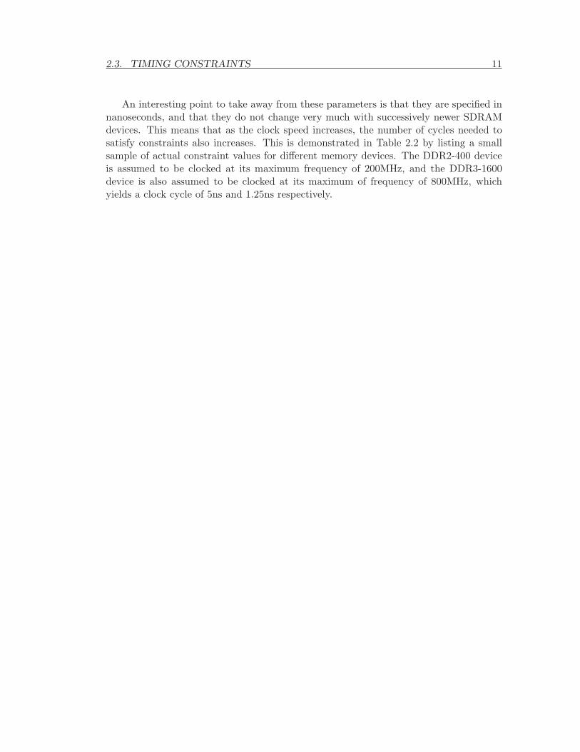
2.3. TIMING CONSTRAINTS 11
An interesting point to take away from these parameters is that they are specified innanoseconds, and that they do not change very much with successively newer SDRAMdevices. This means that as the clock speed increases, the number of cycles needed tosatisfy constraints also increases. This is demonstrated in Table 2.2 by listing a smallsample of actual constraint values for different memory devices. The DDR2-400 deviceis assumed to be clocked at its maximum frequency of 200MHz, and the DDR3-1600device is also assumed to be clocked at its maximum of frequency of 800MHz, whichyields a clock cycle of 5ns and 1.25ns respectively.

12 CHAPTER 2. SDRAM

Memory Efficiency 3To make sensible calculations regarding latency and bandwidth, we need to establish amethod for determining how efficiently a memory behaves. In this section the efficiencymodel of Woltjer [18] is presented. This model is used to differentiate types of efficiencies.Once these efficiencies are known, they may be used to calculate the amount of bandwidthprovided by an SDRAM memory controller.
3.1 Peak Bandwidth
Definition 3.1 (Peak Bandwidth) Peak bandwidth is the maximum number of bytes
per second that can be transferred on the data bus.
Computing the peak bandwidth is important as this number represents the maximumbandwidth offered by a memory. Inefficiencies introduced by physical characteristics of anSDRAM can significantly lower the actual amount of bandwidth provided to a resource.
If we let DataBusWidth equal the width in bits of the data bus, and ClockFrequencybe the frequency of the clock, then we have
bandwidthpeak =ClockFrequency cycles
second∗
2 bursts
cycle∗
DataBusWidth bits
burst∗
1 byte
8 bits(3.1)
As an example, if we had a DDR2-400 SDRAM device running at 200MHz with a 16bit data bus we have
bandwidthpeak =200M cycles
second∗
2 bursts
cycle∗
16 bits
burst∗
1 byte
8 bits= 800 MB/s
Most memory controllers are unable to provide this amount of bandwidth due tophysical characteristics of an SDRAM, such as refresh. In order to properly calculatethe worst-case bandwidth offered by a given memory, we must examine areas of SDRAMoperation where efficiency is lost.
3.2 Data Efficiency
Definition 3.2 (Data Efficiency) Data efficiency is the amount of data requested by
a component compared to the actual amount of data returned by the memory controller.
Data efficiency is traffic dependent, and therefore cannot be computed at design timeunless we know some information about the requestors using the memory controller.Specifically, we need to know the granularity of the memory, as well as the sizes ofrequests of the resources.
13

14 CHAPTER 3. MEMORY EFFICIENCY
Often, the amount of data requested does not exactly match the amount of data ac-tually returned by a memory. This occurs because there can be many types of processingelements performing different actions, that share one memory. Because the requestors’application requirements may be very different, it is possible that the amount of databeing requested may also be very different. Thus, frequently a requestor is given moredata than it requires, and must throw away the excess. This data that is thrown awayis representative of the data efficiency.
As seen in Equation (3.2), the severity of the loss in efficiency is dependent on therequest size. Requestors with a small request size using a memory with a large granularitywill have extremely poor data efficiency. As we see later in Section 3.6, this translates topoor actual bandwidth as well. Thus, data efficiency can change significantly dependingon the resources using the memory controller. Experimentally, it has been observed thata data efficiency of 75% is expected for an MPEG-2 stream [18].
edata =sizerequest
granularitymemory
(3.2)
As an example, we examine Figure 3.1 and assume a requestor wants to read 6 words.However, the granularity of this memory is such that it provides 4 words per read burst.Thus, in order to provide 6 words to the requestor, 2 read commands must be sent.Therefore edata in this case is 6/8, or 75%.
BUSDATA DO DODODODODODODO
BUSCOMMAND ACT 0 RD 0 RD 0
time
Figure 3.1: Visual representation of bank efficiency. Blank slots in the command busrepresent NOP commands.
3.3 Bank Efficiency
The time taken to access a memory cell is highly variable for SDRAMs. If a readcommand is sent to a bank which currently has a different row already activated, thecontroller must first precharge the current row, activate the new row, and then sendthe read command. This penalty is captured in the bank efficiency. By examiningthe amount of cycles that data is on the bus, compared to the total number of cyclestaken to get that data on the bus, we are able to compute this value. Bank efficiencyis dependent on the memory map chosen, as we shall see in Section 4.2. As the bankefficiency is dependent on the addresses of requests, which are not known at design time,we cannot place a useful bound on bank efficiency.
If we examine Figure 3.1, we are also able to compute the bank efficiency of thispattern. In this particular period, we see 4 cycles where there is data on the bus, andthat the entire length of this group of commands is 10 cycles long. Therefore the bankefficiency is 40%.
3.4. SWITCHING EFFICIENCY 15
ebank =DataCycles
TotalCycles(3.3)
3.4 Switching Efficiency
SDRAMs require a time buffer between a read and write command, such that the direc-tion of the data bus can be reversed. This often results in cycles where no data can beon the bus. Thus, we must take this drop in efficiency into account by examining thedifference between the time taken for a read and write command, compared to the timetaken for a read and write commands, plus their respective switching costs. According toWoltjer [18], traffic consisting of 70% reads and 30% writes yields a switching efficiencyof 93.8%.
In general, the switching efficiency is not possible to compute at design time as theread to write switching frequency is not known at design time. However, in Section 5 wesee how some design decisions allow us to compute this value.
3.5 Refresh Efficiency
Every SDRAM must be refreshed periodically in order to maintain the integrity of thestored data. However, in order for a refresh to occur, all activity must cease, and all banksmust be precharged. Refresh efficiency is used to determine how much the effectivenessof the memory is changed due to the lost time introduced by the refresh command.
Therefore we compute erefresh as the amount of time in a period where the memoryis not busy with refresh commands. tref refers to the amount of time taken for a refreshcommand to be executed, and tperiod is the period in which refreshes are executed.
erefresh = 1−tref
tperiod
(3.4)
Refresh efficiency is not traffic dependent and therefore can be calculated at designtime. Due to the very long refresh period (7.8 µs at normal operating temperatures)compared to the time taken to execute a refresh command (on the order of 100 ns), therefresh efficiency is usually around 99%.
3.6 Net Bandwidth
Definition 3.3 (Net Bandwidth) Net bandwidth is the actual amount of bandwidth
provided by the memory to requestors.
The concern of applications using this memory controller is directed at the net band-width, as this is the amount of bandwidth they are actually provided. It is calculatedby simply finding the product of the above efficiencies and the peak bandwidth, withone exception. edata is not taken into account due to the way bandwidth allocationand requestor requirements are handled by our memory controller. As we shall see in

16 CHAPTER 3. MEMORY EFFICIENCY
Section 7.1.1, edata is factored into the requestor’s requirements. Thus, the equation forcalculating bandwidthnet becomes,
bandwidthnet = ebank ∗ eswitch ∗ erefresh ∗ bandwidthpeak (3.5)

Memory Controllers 4A memory controller is the interface between an SDRAM and the system. By having itas a separate unit, the system utilizing the SDRAM does not need to worry about timingconstraints and other details of a specific SDRAM, and can simply treat the device as ageneral memory.
Specifically, a memory controller is responsible for the following tasks:
• Memory Mapping
• Command Generation
• Command Scheduling
PhysicalAddress
SDRAMCommands
LogicalAddress
MUX
DataBus
CommandBus
NetworkOnChip
Memory
MemoryMapping
CommandGenerator
MUX
Memory Controller
Write Data
Read Data
Requestor
Requestor
Requestor
Arbiter
ResponseBuffer
RequestBuffer
Figure 4.1: Architecture of a memory controller.
The controller works by first accepting some requests from external IP blocks, andthen storing them into request buffers. The addresses are then translated into the phys-ical address space by means of a memory map, after which they are scheduled by thearbiter, and converted to memory commands by the command generator. The responsefrom the memory is then sent back to the response buffer, and from there it will be sentback to the requestor.
4.1 Arbiter
The arbiter is responsible for determining which outstanding request is allowed to be sentto the memory controller. The logic for choosing which request ought to be scheduled
17

18 CHAPTER 4. MEMORY CONTROLLERS
depends on the type of system in which the controller is used. Some systems value lowpower use, some value high efficiency, and some value soft or hard real-time requirements.The characteristics of requests that the arbiter looks at are the requirements of therequestor, and optionally, the current state of the memory device.
4.2 Memory Mapping
A memory map provides a translation between logical memory and physical memoryaddresses. Thus, to a requestor, a memory looks like one large continuous array, whilein reality the memory is organized into separate banks, rows, and columns. The choiceof memory mapping is important as it has a large effect on latency and bandwidth, asseen in the following sections.
4.2.1 Continuous Memory Map
One type of translation used is called the continuous memory map. It is called suchbecause successive addresses in the logical space are mapped to successive addresses ina single row in a single bank. Thus, the same row is accessed over and over again untilthe end of the row is met. At this point the mapping may switch to a new bank or toa new row in the same bank. As a result, row activation cost needs only to be incurredonce in order to access a significant amount of successive data.
A continuously mapped address space can be seen in Figure 4.2. The memory pre-sented is a highly simplified design for clarity. The memory has 4 banks, each with a 2by 2 array of memory cells. Therefore 1 bit is needed to represent the column and rowrespectively, and 2 bits for the bank address. Thus, in total 4 bits are required for thelogical address. As can be seen, if the least significant bit of the logical address is mappedto the column address, the next 2 significant bits are mapped to the bank address, andthe final bit is mapped to the row address, we achieve a continuous memory map.
Column
Logical Address
Memory Map
Row
0
1
0 1
Bank 0 Bank 1 Bank 2 Bank 3
10
2 3
11 12 13
4 5 6
14 15
7
R[0] B[1] B[0] C[0]
3 2 1 0
98
0 1
Figure 4.2: Illustration of a continuous memory map.
This type of mapping can be very beneficial to bandwidth and latency when thesystem has a low number of requestors, and the data being considered exhibits data

4.2. MEMORY MAPPING 19
locality. Consider a system with a single requestor, who requests data from consecutivelogical addresses, as seen in Figure 4.2. If this requestor wants to send 4 read commandsstarting at bank 0, row 0, column 0, then we see that the memory controller needs tosend an activate command to bank 0, and an activate to bank 1, and 2 reads to eachbank. The resulting group of commands is shown in the top graphic in Figure 4.3.
BUSDATA
BUSCOMMAND
BUSDATA
BUSCOMMAND RD 0 RD 0ACT 1 RD 1 RD 1
D1 D1 D1 D1 D1 D1 D1 D1
D2 D2 D2 D2D3 D3 D3 D3
time
ACT 0
DODODODO D1 D1 D1 D1
time
ACT 0
DODODODODODODODO
RD 0 ACT 1 RD 1 ACT 2 RD 2 ACT 3 RD 3
Figure 4.3: Example of commands generated for a continuous memory map (top) andan interleaving map (bottom). The data bus has been wrapped back onto itself.
A significant problem occurs when we examine the sequence of commands generatedin the worst-case scenario. We see in the top graphic of Figure 4.6 that when a requestoris trying to access different rows in the same bank, the efficiency of the memory controllerdrops significantly. This occurs because the minimum time between sending an activatecommand to the same bank is quite large.
Another issue occurs when the number of requestors begins to grow. The effectivenessdrops significantly because of different requestors all sharing the same row buffer in abank. With high numbers of requestors, the frequency of overwriting a given bank’s rowbuffer increases, and this type of mapping becomes less viable.
As mentioned above, the use of continuous memory maps are limited to use caseswhere there are a low number of requestors. However, there is a method that maybe employed to alleviate this problem, called bank partitioning. Bank partitioning isachieved by funneling requests from different requestors statically into different banks.In this way, the row buffers are not scrambled by interfering requestors assuming thereare fewer requestors than the number of banks. However, to do this we must makeassumptions regarding the number of requestors. A design goal of this thesis is to notmake any assumptions regarding the number of requestors in the system, and thus wehave chosen to not employ bank partitioning.
4.2.2 Interleaving Memory Map
The alternative type of translation to a continuous memory map is called an interleavingmemory map, and is shown in Figure 4.4. This style of translation is called interleavingbecause successive bursts of accesses in the logical address space are mapped to differentbanks in the physical address space. Initially, we might expect a performance reductionas every bank must now be activated before it is accessed. However, there is a memoryrequirement that prevents a read or write command from being issued to the memoryimmediately after an activate command. Thus, there are some wasted cycles. In an

20 CHAPTER 4. MEMORY CONTROLLERS
interleaving memory map we can insert an activate command to a different bank whilewaiting to be allowed to schedule a read or write command. If the requested size ofdata is large enough, the cost of activating all banks can be ameliorated. Thus, theeffectiveness of the interleaving memory map increases as the granularity of the accessesincreases.
14
Logical Address
Memory Map
3 2 1 0
C[0] R[0] B[1] B[0]
Row
Column0 1
0
1
0
4 12
8
Bank 0 Bank 1
1
5
9
13
Bank 2
6
2 10 3
7
11
15
Bank 3
Figure 4.4: Illustration of an interleaving memory map
Another benefit of great importance to the goals of this thesis is that we want to placea useful bound on worst-case bandwidth. The problem that the continuous memory mapsuffered from in the worst-case scenario was that the activate to activate constraint onthe same bank creates large gaps between the access commands. With the interleavingmemory map, we are not concerned about activating the same bank repeatedly, butrather activate different banks. The constraints governing the minimum time betweenactivates to different banks is much less strict than its same bank counterpart, thereforethe number of cycles to produce the same amount of data in the worst-case is significantlyless when using an interleaving pattern.
Therefore the benefits of this approach are that the latency to access a word is notdependent on the state of the SDRAM, and activate command costs can be reduced.Because this mapping makes no assumptions about the type of data being used, orabout the number of requestors in the system, and for the benefits detailed above, theinterleaving map has been chosen as the type of memory map to be used.
To demonstrate this benefit we examine two examples. If we compare the lengthof time for sending 4 read commands with a continuous memory map in the best-casescenario, compared to an interleaving memory map, we see that the continuous map pro-duces the same amount of data with many fewer clock cycles. This is seen in Figure 4.5.This shorter pattern sequence translates to a higher bandwidth for the continuous mem-ory map due to a higher bank efficiency, as shown in Equation (3.3).
However, in Figure 4.6 we compare the length of time for executing 4 read commandswith a continuous memory map in the worst-case scenario, against an interleaving mem-ory map, we see a much different result. The worst-case scenario occurs when requestscoming into the memory controller wish to read from different rows in the same bank.As we stated in our goals for the thesis, we want to place useful bounds on worst-case

4.3. COMMAND GENERATOR 21
bandwidth, therefore we have chosen to use the interleaving memory map, as it providesbetter worst-case performance.
time
BUSCOMMAND ACT 0 RD 0 ACT 1 RD 1 ACT 2 RD 2 ACT 3 RD 3
BUSCOMMAND RD 0 RD 0 RD 0 RD 0ACT 0
10 Cycles
16 Cycles
Figure 4.5: Illustration of best-case scenario when using a continuous memory map (top)compared to an interleaving memory map (bottom)
.
BUSCOMMAND ACT 0 RD 0ACT 0 RD 0 7 CyclesACT 0 RD 0 7 Cycles ACT 0 RD 0 7 Cycles
37 Cycles
BUSCOMMAND ACT 0 RD 0 ACT 1 RD 1 ACT 2 RD 2 ACT 3 RD 3
16 Cyclestime
Figure 4.6: Illustration of worst-case scenario when using a continuous memory map(top) compared to an interleaving memory map (bottom)
.
4.3 Command Generator
The command generator is responsible for producing SDRAM memory commands basedon requests in the request buffer, depending on the memory map chosen. The generatormay need to be aware of the current state of the SDRAM device. If a requestor is tryingto read a word of data from a bank, often the row in the bank is not already in the rowbuffer, therefore the controller must first activate the row in the bank, and then it maysend the actual read command to retrieve the data. The generator must be configuredto type of SDRAM device being used, as each type requires different amounts of timebetween commands.
4.4 Types of Memory Controllers
Based on the memory controller components defined previously, this section gives anoverview of the various types of memory controllers used today.
4.4.1 Statically Scheduled Memory Controllers
Statically scheduled controllers work by having a predefined order of commands pro-grammed at design time. These controllers are used in systems where there is no unpre-dictability in the traffic, and thus everything is static. If there is any variation in the readto write ratio of commands, or if the bandwidth requirements change, then the currentschedule becomes invalid. In order to remedy this, one can consider creating a static

22 CHAPTER 4. MEMORY CONTROLLERS
schedule for every use case that the system may encounter, however this number maybecome very large. To overcome these problems, a new type of controller was developed,and we examine it in the next section.
4.4.2 Dynamically Scheduled Memory Controllers
In the above section, we saw that statically scheduled controllers cannot perform wellwhen the traffic in question varies over time. Thus, a new type of controller was invented;the dynamically scheduled memory controller. This controller works by generating com-mands at run time depending on requests. It then attempts to optimize the actualcommand schedules based on the current outstanding requests, and this can be donewith command reordering [14], a self-optimizing controller [7], and other techniques [15].
Command reordering is mechanism by which a memory controller attempts to im-prove average-case efficiency. It can accomplish this with command grouping, where thecontroller groups similar commands together to reduce the number of data bus directionchanges, and bank grouping, which means the controller separates requests by bank.Then, each bank determines when it should schedule an outstanding request dependingon a selectable policy. Bank reordering has been shown to improve sustained bandwidthby up to 144% over a system without reordering when applied to realistic syntheticbenchmarks [14]. An example of command grouping in shown in Figure 4.7. This ex-ample demonstrates how two commands can be reordered to improve efficiency. In theupper figure we see that if the controller were to execute these requests in order, thatthere would be 3 changes in data bus direction, whereas after commands are reordered,there is only one change in direction. This offers a significant increase in bandwidth,however, the amount of time until command 2 is executed has now been increased.
RD 0 WR 3RD 2 WR 1
RD 0 WR 1 WR 3RD 2
1 432
In order execution
Reordered execution
Figure 4.7: Illustration showing reordering of commands to reduce data bus directionchanges. The top figure shows the requests in order, the bottom figure shows the requestsreordered.
Another method of improvement mentioned above was a self-optimizing controller.During the operation of this controller, it is constantly examining the long term impactsits schedules have on memory efficiency. If it begins to see a shift in the incomingrequests, it optimizes the schedules to produce the best possible patterns. It has beenshown to increase the net bandwidth of a multiprocessor system by 30% over a systemwith in-order scheduling [7].

4.4. TYPES OF MEMORY CONTROLLERS 23
These optimizations can greatly increase the average-case latency and bandwidthat the cost of the worst-case latency and bandwidth. Because commands are possiblyreordered during runtime, it becomes very difficult to analytically determine the absoluteworst-case latency and net bandwidth. As such, simulations are the only way to try andverify if bounds are met. As a result, only ranges and averages are returned as verificationfor system traces that have been simulated. In a system with hard real-time deadlinesthis type of verification could be unacceptable, and therefore these dynamically scheduledmemory controllers are not suitable for this thesis.
4.4.3 Hybrid Memory Controllers
To provide useful performance to a system with variable traffic without sacrificing hardreal-time requirements, a new memory controller has been proposed [2].
This controller works by combining aspects of both the statically scheduled controllerand dynamically scheduled controllers. A set of groups of commands are utilized by thecontroller to interact with the memory. Each one of these groups of commands, referredto as a pattern, is responsible for one type of interaction. There is a read pattern, awrite pattern, a read to write switching pattern, a write to read switching pattern, anda refresh pattern. These patterns are generated at design time, and their constructionis governed by the constraints in the memory specification and limited by requestorrequirements.
The idea that separates this controller from a statically scheduled controller, is thatthis controller schedules these precomputed patterns dynamically, using a predictablearbiter.
Dynamic scheduling with a predictable arbiter allows us to bound the worst-caselatency, while knowing the patterns in advance lets us bound the worst-case bandwidth.Another benefit of this approach is that by placing the commands into larger groups, wesimplify the amount of constraints present. The patterns generated at design time areexplored in Section 5. A demonstration of the differences among the memory controllersintroduced above is shown in Table 4.1.
Table 4.1: Comparison of characteristics of different memory controllers.Controller Commands Arbiter Predictability Cost Complexity
Dynamic Dynamic Dynamic No Bad Worst-Case High
Predator Static Dynamic Yes Dependent on edata Medium
Static Static Static Yes Rigid Design Low

24 CHAPTER 4. MEMORY CONTROLLERS

Memory Patterns 5Memory patterns are sequences of SDRAM commands, and are used by the hybridmemory controller proposed in Section 4.4.3. In this section, we present an overviewof the patterns, followed by descriptions of the individual patterns themselves. Later,we discuss how these patterns can be evaluated in terms of their efficiency, latency, andbandwidth.
5.1 Pattern Overview
Patterns provide the only mode of interaction between a memory controller and thememory itself. We have divided the types of patterns into two groups: access patternsand auxiliary patterns.
Read patterns and write patterns are grouped under access patterns as they are theonly patterns that can actually access the contents of the memory. Once the accesspatterns have been determined, they are used to compute the lengths of the auxiliarypatterns.
The remaining patterns are auxiliary patterns. These patterns consist of the read
to write switching pattern, the write to read switching pattern, and the refresh pattern.These patterns perform more of a support role, and are responsible for giving the databus time to switch direction, and keeping the data cells in the memory charged.
5.1.1 Scheduling Rules
The patterns are constructed in such a way that a read pattern may be immediatelyscheduled after itself. Similarly, write patterns are also constructed in such a manner.The reason this is done is to reduce the number of patterns required to interact with amemory device.
When a switch occurs from a write pattern to a read pattern, a write to read switchingpattern must be executed. This provides the SDRAM with the required time to alter thedirection of the data bus. Similarly, a read to write switching pattern must be executedwhen the memory controller wants to execute a write pattern when a read pattern hasjust finished. A refresh pattern may be executed after read and write patterns. Switchingpatterns are not required after a refresh. An example of a sequence of patterns can beobserved in Figure 5.1.
READ READ RTW WRITE WTR READ REFRESH WRITE
Figure 5.1: Sequence of various patterns.
25

26 CHAPTER 5. MEMORY PATTERNS
5.2 Types of Patterns
Detailed in this section are the types of patterns used by the Predator memory controller.
5.2.1 Access Patterns
A read pattern is used to retrieve data from the SDRAM. There is one activate commandper bank. Each activate is followed by BurstCount read commands to each bank, in aninterleaved fashion. BurstCount is defined in Definition 5.2. Wherever there are gapsremaining, they are filled with NOP commands. Similarly, a write pattern is constructedthe same way with write commands instead of read commands.
In Figures 5.2 and 5.3, we see two examples of valid patterns for a DDR2-400 SDRAMdevice. The definition of a valid pattern is seen in Definition 5.1.
Definition 5.1 (Valid Pattern) Valid patterns are defined as patterns that do not vi-
olate any of the constraint timings of a given SDRAM.
Definition 5.2 (BurstCount) BurstCount is the number of read or write commands
per bank present in a read or write pattern.
ACT 0 RD 0 ACT 1 RD 1 ACT 2 RD 2 ACT 3 RD 3
16 Cycles
Figure 5.2: Read pattern for DDR2-400 SDRAM. Blank schedule slots indicate NOPcommands.
ACT 0 ACT 1 ACT 2 ACT 3WR 0 WR 1 WR 2 WR 3
16 Cycles
Figure 5.3: Write pattern for DDR2-400 SDRAM.
5.2.2 Auxiliary Patterns
The read to write switching pattern is used to provide time to the SDRAM so that itmay change the direction of its data bus. This pattern only contains NOP commands,the number of which is dependent on the required distance between a read and writecommand as stated by the memory specification. The write to read switching pattern isconstructed in the same way, except it is used in the transition between a write patternand a read pattern.
As a side note, sometimes this switching time may be completely mitigated dependingon the SDRAM specification and the pattern chosen.
The refresh pattern contains one refresh command, along with a number of NOP com-mands. The number of NOP commands, and the exact location of the REF command,are governed by the read and write pattern construction.

5.3. PATTERN DOMINANCE 27
NO
P
NO
P
NO
P
NO
P
NO
P
NO
P
NO
P
NO
PREAD READ WRITE WRITE READ
RTW WTR
NO
P
NO
P
NO
P
NO
P
NO
P
Figure 5.4: Switching patterns being used between read and write patterns.
Definition 5.3 (Pattern Set) A pattern set is the collection of read, write, read to
write switching, write to read switching, and refresh patterns that are generated for a
particular memory specification and BurstCount.
5.3 Pattern Dominance
When computing the various types of efficiencies and latencies for a given pattern set, itis important to determine which sequence of patterns will produce the worst-case latencyand bandwidth. There are 4 categories into which a pattern set may fall. These are, readdominance, write dominance, mix read dominance, and mix write dominance. Below,we have outlined how to calculate the different dominance types. tread, twrite, trtw, twtr,and tref refer to the amount of time taken to execute the respective pattern in a set.
5.3.1 Read Dominance
Read dominance is said to occur when the length of a read pattern is greater than thesum of the read to write switch, write, and write to read switch patterns. Thus, whenattempting to compute the worst-case latency of a pattern, one should assume that onlyread patterns are being executed by the controller. An example of a read dominantpattern set is shown in Figure 5.5
tread > twrite + twtr + trtw (5.1)
RTW WRITE WTR
READ
Figure 5.5: Illustration of read dominance.
5.3.2 Write Dominance
Write dominance is the converse of read dominance. When calculating worst-case latencyor bandwidth, one should assume that only write patterns are being executed. Anexample of this can be seen in Figure 5.6.
twrite > tread + twtr + trtw
(5.2)

28 CHAPTER 5. MEMORY PATTERNS
This may be rewritten as
tread < twrite − twtr − trtw (5.3)
WRITE
READ RTWWTR
Figure 5.6: Illustration of write dominance.
5.3.3 Mix Dominance
When a set of patterns does not fall into the read or write dominance areas, it must fallinto the mixed dominance area. This area is reached when alternating between read andwrite patterns provides the worst-case scenario.
tread + trtw + twrite + twtr ≥ 2 ∗ tread ∧
tread + trtw + twrite + twtr ≥ 2 ∗ twrite
This may be rewritten as
twrite − twtr − trtw ≤ tread ≤ twrite + twtr + trtw (5.4)
WRITE
READ RTWWTR
READ
WRITERTW WTR
Figure 5.7: Illustration of mix dominance.
Mixed dominance is further subdivided into two more areas; mixed read and mixedwrite dominance, in order to further simplify the calculations needed to determine worst-case latency and bandwidth. Mix read dominance means that the sum of lengths of readand write to read switch patterns is larger than the sum of write and read to write switchpatterns. The bandwidth offered by a pattern set of mix read or mix write dominancedoes not change, as the sum of the lengths of the patterns remains constant, however thelatency calculations may produce different results depending on which dominance typethe pattern exhibits.

5.4. EFFICIENCY CALCULATIONS 29
twtr + tread ≥ trtw + twrite
tread ≥ twrite − twtr + trtw (5.5)
Mix write dominance means that the sum of write and read to write switch patternsis larger than the sum of read and write to read switch patterns.
trtw + twrite > twtr + tread
tread < twrite − twtr + trtw (5.6)
Figure 5.8 shows the range of dominance types on a line. In this figure tread is scaledup and down while keeping twrite, twtr, and trtw fixed.
Mix Write Dominant Mix Read DominantWrite Dominant Read Dominant
Mix Dominant
tread = twrite − twtr − trtw
tread = twrite − twtr + trtw
tread = twrite + twtr + trtw
tread + +tread −−
Figure 5.8: Dominance scale viewed on a line.
5.4 Efficiency Calculations
As mentioned in Section 3, the efficiency of a memory controller is very important. It isa major component of the net bandwidth equation shown in Equation (3.5). Therefore,in order to accurately calculate the bandwidth provided by the memory controller, weneed to know the efficiency values. Now that we have defined the tools used by a memorycontroller to interact with an SDRAM, we can precisely compute the various efficiencies.Additionally, the efficiency model of Woltjer that is used by Predator is extended toaccommodate pattern sets where the read and write patterns are of different lengths. InSection 3, we concluded that it was difficult to compute some of the efficiencies at designtime due to not knowing the traffic. We bypass this restriction now because we haveinterleaving patterns with fixed access granularity, and shift all uncertainty into dataefficiency.
5.4.1 Bank Efficiency
From Section 3.3, we saw that the bank efficiency was a way to incorporate the loss incycles incurred as a result of SDRAM access time variability.

30 CHAPTER 5. MEMORY PATTERNS
The bank efficiency is now computed as the number of cycles that there is dataon the bus (TransferCycles), as defined in Equation (5.7), divided by a pattern lengthdetermined by the pattern set dominance type as seen in Equation (5.8). DataRate isthe number of words per clock cycle, BurstSize is the number of words per read or writecommand, and BurstCount is the number of read or write bursts sent to a particularbank. The reason that we divide by the average pattern length in Equation (5.8) in thecase of mix dominance is because in the worst-case we will have equal amounts of bothtypes of patterns being executed.
TransferCycles =BurstCount ∗BurstSize ∗NumberOfBanks
DataRate(5.7)
ebank =
TransferCyclestread
if read dominant
TransferCyclestwrite
if write dominant
TransferCyclestread+twrite
2
if mix read or mix write dominant
(5.8)
The calculations are now possible because the addresses of requests coming into thememory controller do not affect access times. Due to the interleaving nature of ourpatterns, every access will activate all banks before data is read, and all banks are inan idle state when a pattern begins to execute. Thus, access times become static perpattern.
5.4.2 Data Efficiency
As shown in Section 3.2, the equation for determining the data efficiency is dependent onthe request size of a requestor and the granularity of the memory access pattern. Nowthat the read and write pattern has been defined, and considering that it is the only wayin which a requestor may access data, we can compute specifically the data efficiency.
granularitypattern = BurstCount ∗NumberOfBanks
∗BurstSize ∗DataBusWidth (5.9)
Therefore Equation (3.2) becomes
edata =sizerequest
granularitypattern
(5.10)
5.4.3 Switching Efficiency
When a pattern set exhibits read dominance or write dominance, it implies that theworst-case scenario occurs when only read patterns or only write patterns are beingexecuted. This means that there will be no switches in the worst-case, and therefore theswitching efficiency will be 100%.

5.5. LATENCY CALCULATION 31
If the pattern is mix dominant, the switching efficiency is computed as the time ittakes to execute a read and write pattern divided by the time taken to execute a read,read to write switch, write, and write to read switch patterns. This is due to the factthat in the worst-case read and write patterns are alternated at every opportunity.
eswitch =
1 if read or write dominant
tread+twrite
tread+twrite+twtr+trtwif mix read or mix write dominant
(5.11)
5.4.4 Refresh Efficiency
In order to compute the refresh efficiency, we need to know the worst-case request timethat can occur. Now that this value is easily computable, we can determine the refreshefficiency by taking the amount of time it takes for a refresh pattern to execute, anddividing it by how frequently that refresh actually occurs. All current DDR-SDRAMshave a refresh interval (tREFI) of 7800ns at normal operating temperatures. However,to compute the refresh efficiency, we need to know the worst-case request time thatcan occur. The reason we need to calculate LongestRequestT ime is that a refreshpattern may need to be scheduled right after a read or write pattern has been scheduled.LongestRequestT ime is defined to be the sum of a switching pattern and an accesspattern because in the worst-case, the opposite access pattern has just been executedand thus be must switched. To make sure that the refresh interval is not violated, werewrite the refresh interval to be LongestRequestT ime nanoseconds shorter, as shownin Equation (5.12).
LongestRequestT ime = max(tread + twtr, twrite + trtw)
RefreshPeriod = tREFI − LongestRequestT ime + tref (5.12)
erefresh = 1−tref
RefreshPeriod(5.13)
5.5 Latency Calculation
As mentioned in the problem statement in Section 1.3, we also want to guarantee a boundon worst-case latency. Now that we have precisely defined what the memory patternsare, we may now use them to analytically derive the worst-case latency.
The first latency equations that will be shown will compute the worst-case latencyassuming that there are α other requests interfering.

32 CHAPTER 5. MEMORY PATTERNS
latency(α) =
tread ∗ α if read dominant
twrite ∗ α if write dominant
⌈
α+12
⌉
∗ twtr +⌈
α2
⌉
∗ tread +⌈
α2
⌉
∗ trtw +⌊
α2
⌋
∗ twrite if mix read dominant
⌈
α+12
⌉
∗ trtw +⌈
α2
⌉
∗ twrite +⌈
α2
⌉
∗ twtr +⌊
α2
⌋
∗ tread if mix write dominant(5.14)
However, the above equations assume that no refreshes will occur, and this is not avalid assumption while using DRAMs. Therefore the equations are transformed belowto account for refreshes, with φ defined in Equation (5.18) for clarity.
Equation (5.17) specifies the maximum number of refreshes that can occur with αrequestors interfering. It is broken up into 4 pieces as the worst-case scenario changeswith dominance. Once this equation is obtained, we can multiply it with tref as shownin Equation (5.16) to determine how much time refreshes by themselves can take. Wethen add this to the latency calculated in Equation (5.14) to obtain the final latencyequation, shown in Equation (5.15).
TotalLatency(α) = RefreshTime(α) + latency(α) (5.15)
RefreshTime(α) = tref ∗NumberRefreshes(α) (5.16)
NumberRefreshes(α) =
⌈
latency(α)
φ
⌉
(5.17)
φ =
RefreshPeriod− tread if read dominant
RefreshPeriod− twrite if write dominant
RefreshPeriod− tread − twtr if mix read dominant
RefreshPeriod− twrite − trtw if mix write dominant
(5.18)
5.6 Optimality
Now that we have defined how to calculate various efficiencies, latencies, and net band-width, we need to define what an optimal pattern set is.
Definition 5.4 (Optimality) An optimal pattern set for a given memory specification
is the set of valid patterns that provide the maximum net bandwidth.
The reason why net bandwidth is chosen is two-fold. The first benefit of using this isthat the system can support the addition of new requestors more easily, as there is more

5.6. OPTIMALITY 33
net bandwidth to distribute. Alternatively, the extra net bandwidth can be redistributedto the requestors with the idea that with more bandwidth allotted to them, they cancomplete their tasks sooner. In Section 6.2, we see precisely how these patterns aredetermined.

34 CHAPTER 5. MEMORY PATTERNS

Algorithm Approaches 6Three heuristic algorithm approaches are explored in this section: branch and bound,as-soon-as-possible scheduling (ASAP), and bank scheduling. These approaches explorethe trade-offs between execution time of the algorithm and amount of net bandwidthoffered by the resulting patterns. They are all heuristics as computing optimal patternsis too time intensive. The usefulness of the algorithms is measured by the followingaspects.
• Speed of the algorithm
• Net bandwidth offered by the resulting patterns
6.1 Pattern Generation Design Decisions
When generating the patterns as shown in the following sections, we made 4 designdecisions regarding pattern construction. First, we assume that shorter access patternsoffer more bandwidth than longer patterns. Secondly, the algorithms will only focus oncreating access patterns without regard for auxiliary patterns. Thirdly, we always placean activate command in the first pattern slot. Lastly, we let the algorithms treat allbanks equally.
1. We justify the first decision by examining how pattern dominance is related toworst-case scenarios.
(a) Most importantly, shorter access patterns are always better in terms of latencyand bandwidth, when a pattern set exhibits read or write dominance. Forlatency, a shorter pattern means that we can have more interfering requestorswithout missing deadlines. For the bandwidth aspect, we see that shorterpatterns are better due to the effect of bank efficiency on net bandwidth asshown in Equations (5.7) and (3.5). When we have a fixed BurstCount, thereis always the same amount of transfer cycles, and therefore having a shorterpattern length always results in higher bank efficiency, and thus a higher netbandwidth.
(b) In the case where a pattern exhibits mix dominance, we use the fact thatshorter patterns are better as a heuristic. The reason why we cannot guar-antee that the shortest access patterns provide the most bandwidth in mixdominance pattern sets is that it is theoretically possible for a pattern set tohave an increase in access pattern lengths that results in a larger decreasein the switching pattern lengths. In the experimental cases where this phe-nomenon has been observed, the pattern set has always been read or writedominant.
35

36 CHAPTER 6. ALGORITHM APPROACHES
2. Due to the above decision regarding shortest access patterns offering more band-width, the algorithms will focus only on creating shortest possible access patternswithout regard for auxiliary patterns. In order to create optimal pattern sets formix dominant patterns we would need to compute the auxiliary patterns for everycombination of access patterns at all pattern lengths. This would take an inor-dinate amount of time, which violates our requirement for algorithms to producepattern sets within 48 hours.
3. The third decision we motivate with the following.
(a) First, we consider the case where we have NOP commands before any activatecommands present in a pattern, and the NOP commands are not necessary forthe pattern to be valid. In this case, we would remove the NOP commandswith the justification given above regarding shorter patterns always beingbetter.
(b) In the second case, we consider the situation where we have NOP commandsbefore any activate commands in a pattern, and without the NOP commandspresent the pattern is no longer considered valid. In this case the only possiblereason why the removal of NOPs causes pattern invalidity is because the tRC
requirement is no longer met, or the precharge to activate constraint is nolonger met.
i. In the case where tRC is no longer met, by shifting these NOP commandsto the end of pattern, we have not altered the length of the pattern, whilestill maintaining the requirement of tRC .
ii. If the pattern invalidity would be caused by the precharge to activateconstraint being violated, we see that by shifting NOPs to the end of thepattern also does not violate the constraint for the same reason as thecase for tRC .
The effect of moving NOP commands from the back of an access pattern to thefront of an access pattern can change the size of individual switching patterns asseen in Figure 6.1. Here, we enforce a minimum delay of 12 NOP cycles betweena read pattern and a write pattern, and a delay of 7 NOP cycles between a writepattern and a read pattern. In the upper illustration, the access patterns have theirNOP commands at the front of the pattern while the lower illustration has its NOPcommands at the end. When determining the length of a switching pattern, wemust enforce the minimum number of cycles between the last access of an accesspattern and the first access of the following As shown in the figure, the differencein lengths between the two switching patterns is shifted from one switching patternto the other, in order to maintain the minimum number of cycles between accesses.Because the overall sum of the two switching patterns does not change, we see thatmoving NOPs does not influence the bandwidth of a given pattern set. It mayhave a small effect on latency however, due to the changes in trtw and twtr lengths.These lengths affect latency as shown in Equation (5.14).
The refresh pattern is also affected by the location of NOP commands in the accesspatterns. The length of the refresh pattern is partially determined by the number

6.1. PATTERN GENERATION DESIGN DECISIONS 37
RTW WRITE WTRREAD READ
8 cycles 4 cycles 5 cycles 2 cycles
READ RTW WRITE WTR READ
4 cycles 3 cycles2 cycles 10 cycles
NO
P
NO
P
NO
P
NO
P
NO
P
NO
P
NO
P
NO
P
NO
P
NO
P
NO
P
NO
P
NO
P
NO
P
NO
P
NO
P
NO
P
NO
P
NO
P
NO
P
NO
P
NO
P
NO
P
NO
P
NO
P
NO
P
NO
P
NO
P
NO
P
NO
P
NO
P
NO
P
NO
P
NO
P
NO
P
NO
P
NO
P
NO
P
NO
P
NO
P
NO
P
NO
P
Figure 6.1: Illustration of moving NOPs from back to front of pattern.
of cycles from the last precharge of the previous access pattern. An access patternwith its NOPs at the beginning has its precharges earlier compared to a patternwith its NOPs at the end, thus a few cycles can be saved on the refresh pattern.
Thus, by having NOP commands at the end of the pattern, we do not increase thelength of the access patterns, we give the algorithms a base case to start from, wesave cycles in the refresh pattern, and we significantly reduce the design space ofthe branch and bound algorithm.
4. A final design assumption was that all banks are treated as equal by all algorithms.This means that when the algorithm is looking at available commands to be sched-uled at a certain cycle, it does not consider commands to individual banks, butonly the commands themselves. When a command is selected then the algorithmdetermines the proper target bank for the command. This was done in order toreduce the design space.
6.1.1 Access Pattern Termination
As we have mentioned above we search for the shortest access patterns, which meansthat it becomes critical to know when an access pattern is complete. We determineaccess pattern completeness with the following criteria.
• All commands have been scheduled
• tRC constraint satisfied
• Data bus constraints satisfied
• Precharge constraints satisfied
The first criterion is stems from the obvious fact that we do not want to end a patternbefore all of the commands we must insert have been scheduled. The set of commandsto be scheduled is determined with the following equations.

38 CHAPTER 6. ALGORITHM APPROACHES
numActivates = numBanks
numReads = BurstCount ∗ numBanks For Read Patterns
numWrites = BurstCount ∗ numBanks For Write Patterns
The tRC constraint specifies the minimum amount of cycles that must occur betweensuccessive activate commands to the same bank. Due to the fact that we allow anaccess pattern to be scheduled after itself, this constraint is effectively the minimumtheoretical access pattern length. As we saw in Section 5.1.1, we allow a read pattern tobe scheduled directly after itself, as well as a write pattern to be scheduled directly afteritself. Therefore, we must make sure that in these cases where a pattern is scheduledtwice in a row, that the minimum number of cycles between their activate commands toeach bank has been satisfied.
Data bus constraints are that we must ensure that data that is produced on thedata bus does not conflict with data being produced on a data bus from a future accesspattern. To prevent this from happening we must examine the burstSize parameter,and the dataRate parameter. These parameters refer to the number of words producedper read or write command, and the number of words per clock cycle, respectively. Byknowing these, we can determine how many clock cycles must separate the last accesscommand of one pattern, and the first access command of the following pattern.
The last criterion refers to the fact that before a bank can be activated, it must havebeen precharged already. Therefore it becomes important to know where the prechargeactually occurs in an access pattern. We determine this in two ways, as the read andwrite constraints on a precharge are different.
Under a read pattern, the cycle of precharge for a particular bank is computed byfinding the cycle of the last read command to that bank, cycleLastRead, and the cycleof the activate to the bank, cycleACT , and evaluating Equation (6.1), which comesfrom [8,9].
prechargeCycle = max(cycleLastRead + tRTP ,
cycleACT + tRAS ,
cycleLastRead +burstSize
dataRate+ max(tRTP , 2)− 2) (6.1)
We say that for read and write patterns, a bank has its precharge constraint met ifthe cycle of its precharge is at least tRP cycles before the next activate occurs. Undera write pattern, the idea remains the same yet the parameters involved change. Theprecharge cycle for a write pattern is defined in Equation (6.2).
prechargeCycle = cycleLastWrite + tWL +burstSize
dataRate+ tWR (6.2)
Then we say the precharge requirement for write patterns is satisfied if prechargecycle is at least tRP cycles before the next activate command occurs.

6.2. BRANCH AND BOUND 39
6.1.2 Auxiliary Pattern Computation
As we saw in the previous section, the heuristics of the pattern generation approachesfocus on access patterns. We treat the auxiliary patterns as being dependent on theaccess patterns, which allows us to reduce the size of the design space.
The way to compute the refresh pattern length is as follows. First we determine whichaccess pattern has its precharge cycle happen the latest, as the refresh command is notallowed to occur until a minimum number of cycles has passed since the last precharge.The size of the refresh pattern is defined in Equation (6.3).
tref =
tRP + tRFC + (tread − prechargeCycle) if tread − prechargeCycle <twrite − prechargeCycle
tRP + tRFC + (twrite − prechargeCycle) if tread − prechargeCycle ≥twrite − prechargeCycle
(6.3)
The switching patterns have constraints similar to that of the refresh pattern in thatthere is a minimum number of cycles that must occur between two commands. In thecase of switching patterns, there are two constraints, one for each type of switch. Thisnumber of cycles is defined in the memory specification [8, 9]. However, as the cycle ofthe last non-NOP command in an access pattern is not necessarily equal to the pattern’slength, we use Equations (6.4), and (6.5) to determine the size of the switching patterns.delay is the minimum number of cycles that must occur between the last access of onepattern and the first access of the following pattern.
trtw = max(delay − (cycleF irstWrite + tread − cycleLastRead), 0) (6.4)
twtr = max(delay − (cycleF irstRead + twrite − cycleLastWrite), 0) (6.5)
6.2 Branch and Bound
This algorithm is used to find the minimum length access patterns by searching overall possible access patterns according to the design decisions listed above. When thepattern set found exhibits read or write pattern dominance, this algorithm will produceoptimal results. If the pattern set generated is mix dominant, then we cannot guar-antee optimality. The reason we guarantee optimality in the case of read and writedominance is because switching patterns do not affect the worst-case bandwidth offered.Therefore only access patterns are of concern, and shorter access patterns will alwaysoffer higher ebank than longer options, resulting in a higher net bandwidth, as shownin Equation (3.5). When switching patterns do affect the scenario, we must computethe auxiliary patterns for every combination of access patterns in order to guaranteeoptimality, because the shortest access patterns do not guarantee the shortest switchingpatterns. The amount of time taken to compute this is inordinate. Therefore we use theheuristic.
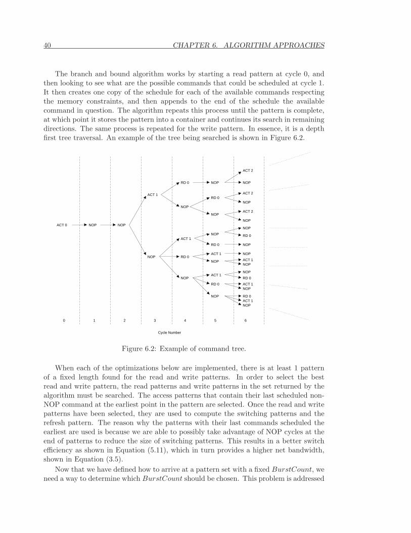
40 CHAPTER 6. ALGORITHM APPROACHES
The branch and bound algorithm works by starting a read pattern at cycle 0, andthen looking to see what are the possible commands that could be scheduled at cycle 1.It then creates one copy of the schedule for each of the available commands respectingthe memory constraints, and then appends to the end of the schedule the availablecommand in question. The algorithm repeats this process until the pattern is complete,at which point it stores the pattern into a container and continues its search in remainingdirections. The same process is repeated for the write pattern. In essence, it is a depthfirst tree traversal. An example of the tree being searched is shown in Figure 6.2.
ACT 1
NOP
1 2 3 4 50 6
ACT 0 NOP NOP
Cycle Number
RD 0
NOP
ACT 1
NOP
RD 0
NOP
NOP
RD 0
NOP
RD 0
ACT 1
NOP
RD 0
ACT 1
ACT 2
NOP
ACT 2
NOP
ACT 2
NOP
NOP
RD 0
NOP
NOP
ACT 1NOP
NOP
RD 0
ACT 1NOP
RD 0ACT 1NOP
NOP
Figure 6.2: Example of command tree.
When each of the optimizations below are implemented, there is at least 1 patternof a fixed length found for the read and write patterns. In order to select the bestread and write pattern, the read patterns and write patterns in the set returned by thealgorithm must be searched. The access patterns that contain their last scheduled non-NOP command at the earliest point in the pattern are selected. Once the read and writepatterns have been selected, they are used to compute the switching patterns and therefresh pattern. The reason why the patterns with their last commands scheduled theearliest are used is because we are able to possibly take advantage of NOP cycles at theend of patterns to reduce the size of switching patterns. This results in a better switchefficiency as shown in Equation (5.11), which in turn provides a higher net bandwidth,shown in Equation (3.5).
Now that we have defined how to arrive at a pattern set with a fixed BurstCount, weneed a way to determine which BurstCount should be chosen. This problem is addressed

6.2. BRANCH AND BOUND 41
Create Switching PatternsCreate Refresh Pattern
Generate Auxiliary Patterns
Set parametersGenerate commands to schedule
Initialization
Determine set of allowed commands at current cycleFork copies of current pattern for each command in the setAppend each command to its forked patternIncrement the current cycleFor each forked pattern, repeat
Schedule Command
Figure 6.3: Flow diagram of the branch and bound algorithm.
in Section 7.
6.2.1 Hard Ceiling
To reduce the run time of the algorithm, some optimizations had to be made. Themost important one was to put a hard ceiling on the pattern length. This prevents thealgorithm from searching for infinite length patterns, and at the same time significantlycuts down on the exploration space. These changes result in significant decreases inmemory and run time.
6.2.2 Sliding Ceiling
This optimization starts where the hard ceiling leaves off. Once a valid pattern is found,its length is recorded and then used as the current maximum ceiling. Thus, when thealgorithm resumes exploring the other branches of the design tree, it first checks to seehow long the current path length is. If it is already over the current ceiling, it stopssearching the current path. This change also results in significant decreases in run timeand memory, as well as a dynamic exploration space.
During the course of this optimization, it is possible that an optimal pattern set ismissed. Previously in Section 6.1, it is stated that shortest access patterns do not alwaysoffer optimal bandwidth.
6.2.3 Sanity Check
This last optimization works in tandem with the sliding ceiling optimization. Wheneverthe algorithm wishes to create a copy of a pattern so that it may append a command, itfirst checks to see if even in the best-case scenario, is it possible for this current pattern’slength to be smaller than the current ceiling, based on the remaining commands to bescheduled into the pattern. As with the other two optimizations, this reduces memoryuse and run time. Pseudo-code is shown for this optimization in Figure 6.4. numActs

42 CHAPTER 6. ALGORITHM APPROACHES
refers to the remaining number of activate commands to be scheduled, numAcc refersto the number of remaining read or write commands to be scheduled.
The first check is based on how many activates are remaining. For example, if thereare 3 activate commands remaining at the current cycle, we can guarantee that thispattern cannot be completed until 2 * tRRD + tRCD cycles have occurred. The 2 *tRRD comes from the fact that activates cannot be scheduled within tRRD cycles ofeach other, and there are at least 2 full delays between activates remaining. The secondpart of the sum is tRCD . This is included into the delay because we know if there is atleast one activate left, there is also at least one read or write access, and tRCD is theminimum delay between an activate command and a read or write command.
The second check looks purely at how many read or write commands are left. If thereare 3 read commands remaining in the pattern, and we know that it there is a minimumdelay of burstSize/dataRate between read commands, then we know that there mustbe 2 full delays of burstSize/dataRate cycles.
if numActs = 0 thenlen1← currentCycle
elselen1← currentCycle + (numActs− 1) ∗ tRRD + tRCD
end ifif numAcc = 0 then
len2← currentCycleelse
len2← currentCycle + (numAcc− 1) ∗ burstSize/dataRateend ifif max(len1, len2) < currentCeiling then
SchedulePossibleelse
ScheduleNotPossibleend if
Figure 6.4: Pseudo-code of sanity check optimization.
6.2.4 Conclusions
The benefit of this algorithm is that it always finds the shortest access patterns. Thistranslates to optimal net bandwidth in the case of read or write dominant pattern sets,but not necessarily optimal net bandwidth in the case of mix dominance. These benefitscome at the cost of run time.
Despite the optimizations that reduce the run time of the algorithm, with high fre-quency SDRAMs, the complexity begins to show itself. Timing constraints are larger,and thus there is more space in between non-NOP commands, which creates many moreoptions when the algorithm is making copies of the current schedule. Furthermore, asthe BurstCount increases, there are more commands to be scheduled, which also signifi-cantly increases the complexity of the design space. In Figure 6.5 the growth in numbersof valid patterns starting with an activate command at different lengths is demonstrated.

6.3. AS SOON AS POSSIBLE SCHEDULING 43
A read and write pattern length of 32 is shortest provided by the branch and bound al-gorithm, while 37 is the length provided by the ASAP algorithm.
1
10
100
1000
10000
100000
1e+06
1e+07
32 33 34 35 36 37
Num
ber
of V
alid
Pat
tern
s
Pattern Length
ReadWrite
Figure 6.5: Number of valid patterns at BurstCount 2 for a DDR2-400 SDRAM device
For practical purposes, the algorithm becomes unusable for online use whenever theBurstCount is greater than 2. Offline use is still practical until a DDR3-1600 is usedwith BurstCount equal to 2. After this point, the run time moves into months andyears. As a result, this algorithm may be used to produce a limited database offline, foruse as a comparator with new algorithms being developed. However, the problem of notbeing able to generate more complicated patterns remains, and thus a new algorithmmust be developed.
6.3 As Soon As Possible Scheduling
This algorithm works by linearly creating a read pattern starting from cycle 0. Thealgorithm looks at the current cycle to see all of the commands allowed to scheduled atthis cycle based on the timing constraints imposed by previous commands. If there ismore than one available command, a priority scheme is used to pick one. The priorityscheme is that read and write commands are selected over activate and NOP commands,and activate commands are chosen over NOP commands. The pseudo-code for thisalgorithm is shown in Figure 6.6, and a flowchart is shown in Figure 6.7.
6.3.1 Conclusions
This major benefit achieved from this algorithm is that it runs extremely fast (lessthan 1 second) for any value of BurstCount. However, this comes at the cost of netbandwidth. As seen in Figures 6.11, 6.12, 6.13, 6.14, the patterns provide around 80%of the bandwidth that is offered by branch and bound algorithm.
The reason this occurs is that it is not always beneficial to schedule a command assoon as it becomes available. After a write command has been issued to the SDRAM,

44 CHAPTER 6. ALGORITHM APPROACHES
currentCycle← 0pattern[currentCycle]← {ACT − 0}while !isV alid(pattern) do
availableCmds← getAllowedCmds(pattern, currentCycle)cmdToSchedule← pickBestCmd(availableCmds)pattern[currentCycle]← cmdToSchedulecurrentCycle + +
end while
Figure 6.6: Pseudo-code of ASAP algorithm
Create Switching PatternsCreate Refresh Pattern
Generate Auxiliary Patterns
Set parametersGenerate commands to schedule
Initialization
Determine set of allowed commands at current cyclePick one command based on priority schemeAppend command to the patternIncrement the current cycleContinue to next cycle
Schedule Command
Figure 6.7: Flowchart of the ASAP algorithm
time is required after the completion of the write to precharge the data in the row buffer.If the algorithm does not account for this, cycles can be wasted.
3 cycles 9 cycles
3 cycles 3 cycles 3 cycles 3 cycles
ACT 0 ACT 1 ACT 2WR 0 WR 1 WR 2 WR 3ACT 3
ACT 0 WR 0 WR 1 WR 2 WR 3ACT 1 ACT 2 ACT 3
Figure 6.8: Example of a pattern generated by the ASAP algorithm (top), and a patterngenerated by the branch and bound algorithm (bottom).
Examine the situation where two write patterns are to be scheduled after each otherand a bank requires 10 cycles after a write command has been issued before it is allowedto be activated again. We also say that the length of the pattern is 16 cycles, the lastcommand is a write command, and that we have the option of scheduling the last activatecommand at cycle 8 or at cycle 12 of the pattern without changing the overall length ofthe pattern.
In this situation, we see that there is potential conflict with the following pattern

6.4. BANK SCHEDULING 45
when the activate is scheduled at cycle 8, thus two extra NOP commands are requiredto be appended to the pattern to satisfy the timing requirement, thereby increasing thelength, decreasing bandwidth, and increasing latency.
In conclusion, this algorithm cut the run time drastically compared to the branchand bound algorithm, yet the difference in net bandwidth provided was too significant toignore. A goal of these algorithm approaches is to provide a high amount of bandwidthand this approach’s net bandwidth is too low. Therefore a new algorithm was developedwith the idea that we were willing to sacrifice a bit in terms of run time for gains in netbandwidth.
6.4 Bank Scheduling
This algorithm was born from the idea that a bank’s activate command should be keptas close as possible to its respective read/write commands. This was done in order toavoid the problems that the ASAP algorithm ran into, shown in Figure 6.8.
The procedure for this algorithm is to first plot an entire schedule for only the firstbank, with all commands placed as closely to each other as possible. Once this is com-pleted the algorithm then plots the schedule for the next bank. The way this part worksis that the algorithm looks for the last read or write command scheduled in the previousbank. The algorithm then places the current bank’s read or write command in the nextallowed slot, assuming that the slot tRCD cycles back in the schedule is allowed to havean activate command placed. The timing constraint tRCD is the minimum number ofcycles between an activate command to a bank and a read or write command to thesame bank. If the pattern does not allow an activate command to be scheduled there,then the read/write command is moved forward one cycle, and the algorithm tries again.This process is then repeated until all banks have been scheduled. The pseudo-code forthis algorithm is shown in Figure 6.9.
pattern[0]← {ACT − 0}pattern[tRCD ]← {RD − 0}currentBank ← 1while !allCmdsScheduled() do
cycleLastRead← getLastRead(pattern)targetCycleRead← cycleLastRead + BL/2while !activateAllowed(targetCycleRead, tRCD) do
targetCycleRead + +end whilepattern[targetCycleRead]← {RD − currentBank}pattern[targetCycleRead− tRCD ]← {ACT − currentBank}currentBank + +
end while
Figure 6.9: Pseudo-code of bank scheduling algorithm

46 CHAPTER 6. ALGORITHM APPROACHES
Create Switching PatternsCreate Refresh Pattern
Generate Auxiliary Patterns
Set parametersGenerate commands to schedule
Initialization
Place ACTSchedule bank 0
Place RDs ASAP
Place RD at earliest slotCheck backward to see ifACT fits, if yes continueto next bank. If not, thenmove RD forward onecycle and repeat
Schedule remaining banks
Figure 6.10: Flow diagram of the bank scheduling algorithm
6.4.1 Sliding Activate
An alternative approach attempted was to let the ACT command slide backwards untilan empty slot is found, as opposed to the READ/WRITE command sliding forwardsimmediately if the slot tRCD cycles behind is not empty. However, the results of thisimplementation were at best the same, and with some memory specifications this imple-mentation proved to yield poorer results than the original implementation.
6.4.2 Conclusions
After running this algorithm, we find that the run time is comparable to that of theASAP algorithm, and therefore suitably fast. More importantly, the closeness to thebranch and bound bandwidth offerings are much more reasonable. As seen in Fig-ures 6.11, 6.12, 6.13, 6.14, the maximal difference between the two is very small. As aresult, this algorithm has been selected for use with Predator. We discuss the integrationof this algorithm in Section 7.
6.5 Results
Plotted in Figures 6.11, 6.12, 6.13, and 6.14, we see comparisons of guaranteed bandwidthoffered by pattern sets generated by the branch and bound, ASAP, and bank schedulingalgorithms. The charts are based on the net bandwidth defined in Equation (3.5).
The bank scheduling approach and the branch and bound approach guarantee simi-lar net bandwidths over different memory specifications. Also observed is the lower netbandwidth guaranteed by the ASAP approach. For all memories tested, branch andbound always provided the best results in terms of offered bandwidth. Bank schedul-ing always matched, or provided slightly less bandwidth than the branch and bound
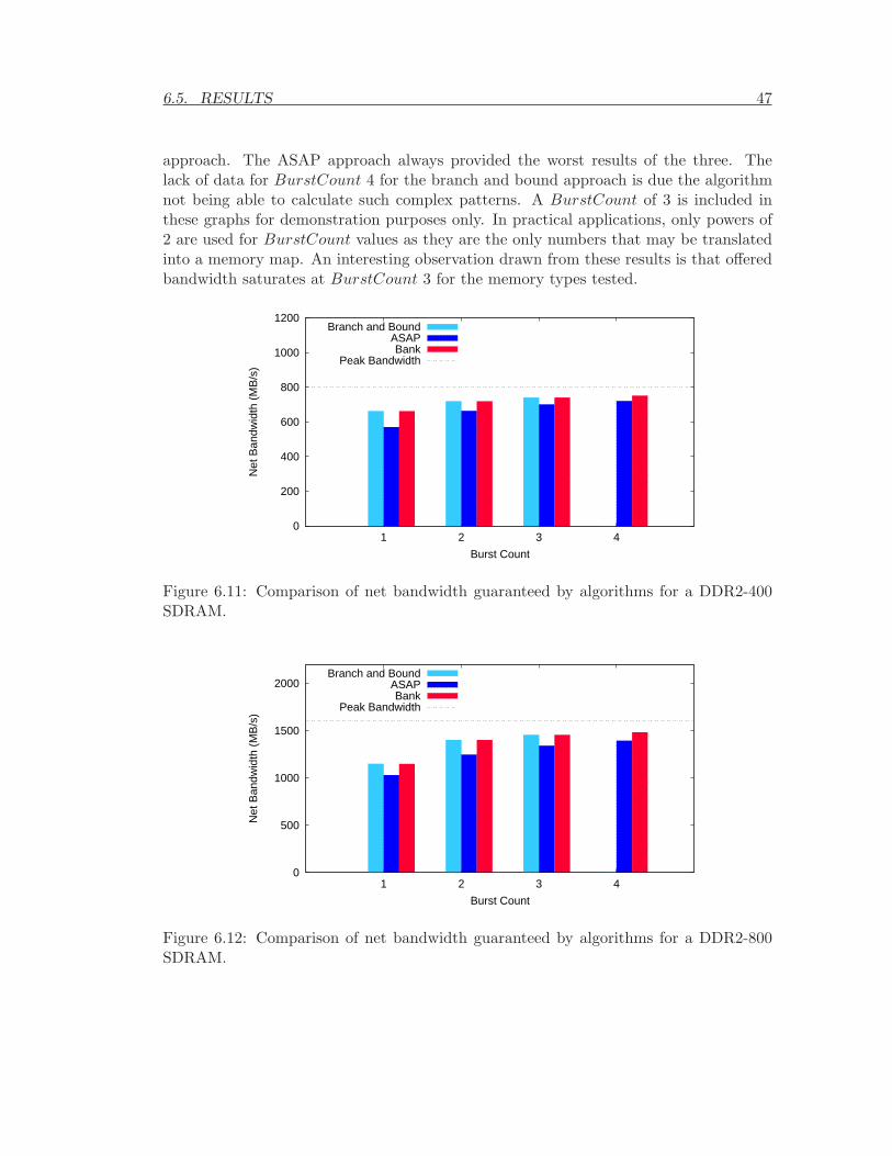
6.5. RESULTS 47
approach. The ASAP approach always provided the worst results of the three. Thelack of data for BurstCount 4 for the branch and bound approach is due the algorithmnot being able to calculate such complex patterns. A BurstCount of 3 is included inthese graphs for demonstration purposes only. In practical applications, only powers of2 are used for BurstCount values as they are the only numbers that may be translatedinto a memory map. An interesting observation drawn from these results is that offeredbandwidth saturates at BurstCount 3 for the memory types tested.
0
200
400
600
800
1000
1200
1 2 3 4
Net
Ban
dwid
th (
MB
/s)
Burst Count
Branch and BoundASAPBank
Peak Bandwidth
Figure 6.11: Comparison of net bandwidth guaranteed by algorithms for a DDR2-400SDRAM.
0
500
1000
1500
2000
1 2 3 4
Net
Ban
dwid
th (
MB
/s)
Burst Count
Branch and BoundASAPBank
Peak Bandwidth
Figure 6.12: Comparison of net bandwidth guaranteed by algorithms for a DDR2-800SDRAM.

48 CHAPTER 6. ALGORITHM APPROACHES
0
500
1000
1500
2000
1 2 3 4
Net
Ban
dwid
th (
MB
/s)
Burst Count
Branch and BoundASAPBank
Peak Bandwidth
Figure 6.13: Comparison of net bandwidth guaranteed by algorithms for a DDR3-800SDRAM.
0
500
1000
1500
2000
2500
3000
3500
4000
1 2 3 4
Net
Ban
dwid
th (
MB
/s)
Burst Count
Branch and BoundASAPBank
Peak Bandwidth
Figure 6.14: Comparison of net bandwidth guaranteed by algorithms for a DDR3-1600SDRAM.

Algorithm Context 7In this section, the overall design flow of the memory controller architecture is examined.Specific attention is given to the integration of the pattern generation algorithm into thePredator configuration flow.
7.1 Tooling Flow Overview
This section provides an overview of the various stages in the offline tool flow. First,the initialization of requestors is considered, followed by a description of the patterngenerator. Lastly, the bandwidth allocator and priority assigner will be discussed.
7.1.1 Requestors
Requestors have their request sizes, latency requirements, and bandwidth requirementsinitialized. The bandwidth requirements require special attention as they are not ini-tialized to the requestor’s specification, but are initialized to a normalized value. Byexamining the pattern granularity and the request size of the requestor, we are able todetermine edata as shown in Equation (3.2). Because we now know which percentageof bandwidth the requestor actually uses, we scale up its requested bandwidth, suchthat the amount it receives meets its requirements. As an example, if a requestor has abandwidth requirement of 200 MB/s, and a request size of 8 bytes, and the pattern setbeing used has a granularity of 16 bytes, then the edata will be 50%. Therefore, we scalethe bandwidth requirement up by a factor of 2, to 400 MB/s. We call this value thenormalized bandwidth requirement. A requestor specification can be seen in Appendix D.
7.1.2 Pattern Generator
The pattern generator is responsible for creating pattern sets. It takes as inputs thefollowing:
• Memory Specification
• BurstCount
The memory specification refers to the timings of the constraints detailed in Ap-pendix A, and an example can be seen in Appendix E. These constraints are verysignificant in determining how the patterns are allowed to be built. As detailed be-low, BurstCount is iterated over, and is therefore needed as an input into the patterngenerator so it knows which pattern to produce.
The outputs of the pattern generator are as follows:
49

50 CHAPTER 7. ALGORITHM CONTEXT
• Read Pattern
• Write Pattern
• Read To Write Switch Pattern
• Write To Read Switch Pattern
• Refresh Pattern
These patterns comprise a pattern set.
7.1.3 Bandwidth Allocator
We consider the case where a credit-controlled static-priority arbiter is used [3]. Thisarbiter’s configuration has two steps: bandwidth allocation and priority assignment.
In the bandwidth reservation mechanism of the arbiter, the bandwidth of the memoryis allocated to the various requestors. The amount of bandwidth requested is approxi-mated by the allocator as closely as possible. However, due to finite precision, discretiza-tion of the bandwidth occurs, which results in the possibility of the allocated bandwidthexceeding the net bandwidth offered by the memory controller. A second issue that isworthy of concern is that the sum of the requested bandwidth of the requestors maysimply be more than the net bandwidth offered by the memory controller. Both of theseissues result in negative non-allocated bandwidth, and are taken into account as shownin the pseudo-code of the algorithm, in Figure 7.1.
7.1.4 Priority Assigner
The priority assignment stage is responsible for finding a priority scheme that allows forall requestors latency requirements to be met. An optimal priority assignment algorithmis used to accomplish this, and it runs in polynomial time [4]. A revision of the latencyequation detailed in Equation (5.15) becomes very useful in this stage.
This equation is needed because it allows us to use a priority assignment algorithmthat is independent of the resource. In essence, the equation is a conversion from actuallatency requirements, to using more abstract requirements, such that the tooling can beignorant of the details of the memory being used.
Equation (7.2) is called the reverse latency equation and its purpose is to find themaximum number of read and write patterns that can interfere before a deadline ismissed in the worst-case. Here, α is defined as the number of interfering patterns, and Θis defined as the maximum latency allowed by a requestor specification, and φ is definedin Equation (5.18).

7.2. INTEGRATION OF PATTERN GENERATOR 51
Θ ≥ TotalLatency(α)
Θ ≥ latency(α) + NumberRefreshes(α)
Θ ≥ latency(α) +
(
latency(α)
φ+ 1
)
∗ tref
Θ ≥ latency(α) +tref ∗ latency(α)
φ+ tref
Θ ≥ latency(α) ∗
(
1 +trefφ
)
+ tref
Θ− tref
1 +trefφ
≥ latency(α) (7.1)
Now, solving for α we get,
α ≤
Θ−tref“
1+tref
φ
”
∗treadif read dominant
Θ−tref“
1+tref
φ
”
∗twrite
if write dominant
Θ−tref
1+trefφ
−3∗twtr
2−tread−trtw
twtr2
+tread
2+
trtw2
+twrite
2
if mix read dominant
Θ−tref
1+trefφ
−3∗trtw
2−twrite−twtr
trtw2
+twrite
2+
twtr2
+tread
2
if mix write dominant
(7.2)
The derivations of these equations can be found in Appendix C.
7.2 Integration of Pattern Generator
Now that the algorithm for use in run time pattern generation has been established, theactual integration into the memory controller flow is explained. Figure 7.1 illustratesthe pseudo-code of the tooling algorithm, and Figure 7.4 shows the architecture of thememory controller.
As we saw in Section 5.6, there is a pattern set for each value of BurstCount. Theproblem for the generator now becomes which BurstCount should be chosen. This isaccomplished by running the pattern generator multiple times with an incrementingBurstCount, and using a new metric that is defined below, to evaluate which generatedpattern set is ideal for a given use case.
We iterate over different values of BurstCount because the pattern generator cannotknow if the pattern set it has created is ideal until bandwidth allocation and priorityassignment have taken place at other values of BurstCount. Therefore, depending on

52 CHAPTER 7. ALGORITHM CONTEXT
BurstCount← 1NonAllocBW ← 0while isNonAllocBWBetter() do
LatencyFlag← 1patternSet← generatePatternSet(memSpec,BurstCount)allocateBandwidth()assignPriorities()for requestor in Requestors do
if requestor.AllocatedLatency > requestor.RequiredLatency thenLatencyFlag← 0 // Latency requirement for requestor not met
end ifend forif LatencyFlag = 0 then
breakend ifBurstCount← 2 ∗BurstCountNonAllocBW ← computeNonAllocBW ()
end whileusePatternSet(patternSet)
Figure 7.1: Pseudo-code of integrated pattern generator.
the result of the output of the allocation and priority assignment, the algorithm mayneed to generate a new pattern at a higher BurstCount.
The reason why the value of BurstCount affects the bandwidth is due to the natureof the patterns. Increasing BurstCount can result in a higher net bandwidth offered bythe pattern because of better bank efficiency. The number of transfer cycles grows bya factor of the BurstCount, while due to the parallelism offered by a bank architectureSDRAM, the length of the pattern typically increases at half that rate. Therefore thebank efficiency increases as shown in Equation (5.7).
However, using a higher BurstCount can also prove detrimental to the net band-width, due to its effect on data efficiency. If we imagine a situation where a requestoronly wishes to read 4 bytes of memory, and a pattern set has an access granularity of 8bytes, we can see that by increasing the BurstCount we increase the access granular-ity even more, which results in a worse data efficiency. As shown in Equation (3.5), adecreasing data efficiency results in lower net bandwidth offered.
Therefore we must iterate over different values of BurstCount in order to find thepattern set that maximizes bank efficiency and data efficiency. In order to do this overdifferent values of BurstCount, we need to establish a loop between the pattern generatorand the flow into which it is set. The flowchart can be seen in Figure 7.3. To demonstratethe relationship between edata and ebank, a plot of a DDR3-1600 SDRAM memory devicehas been created in Figure 7.2. In this graph we see how increasing BurstCount improvesebank at the cost of edata. Also plotted is the non-allocated bandwidth. The goal of theintegrated pattern generator is to find the value of BurstCount that produces the peaknon-allocated bandwidth.
The method that has been implemented is to generate an initial pattern with a

7.2. INTEGRATION OF PATTERN GENERATOR 53
0
0.2
0.4
0.6
0.8
1
1 2 3 4 5 6 7
-1500
-1000
-500
0
500
1000
1500
2000
Effi
cien
cy
Non
-Allo
cate
d B
andw
idth
(M
B/s
)
BurstCount
ebankedata
Non-Allocated BW
Figure 7.2: Trade-off between edata and ebank.
TimingConstraints
BandwidthRequirement
Normalized
NormalizedLatencyRequirement
PatternSet
PatternSet
PatternSet
RequestorSpecificationSpecification
Memory
PriorityAssignmentAllocatorGenerator
Termination condition not met?Save patterns, incrementburst count, and generate thenext patterns
Termination condition met?Stop. Look at completedpatterns to determine whichburst count provides themost non−allocated bandwidth
Pattern STOPBandwidth
Figure 7.3: Flow of integrated pattern generator
BurstCount of 1. If the requestors’ bandwidth requirements are met, then the patternset generated is sent to the service allocation stage, where the bandwidth is discretizedto the various requestors. The patterns are then to the priority assignment stage of theflow.
At the priority assignment stage the arbiter attempts to find a priority scheme forthe requestors such that the latency requirements of no requestor are violated. If thearbiter is able to successfully find an assignment where none of the latency requirementsare violated, then it means that the generator has found a valid pattern set. Then, thenon-allocated bandwidth is computed for the pattern set. If it is less than the valuefound for the previous BurstCount, then the loop is broken. Additionally, if the arbiteris not able to find a priority scheme to fit the pattern set, the loop is broken. Otherwise,the pattern is saved for later consideration, and the loop continues with an incremented

54 CHAPTER 7. ALGORITHM CONTEXT
BurstCount.
The loop termination condition is always reached. The non-allocated bandwidth canonly decrease when edata has become less than 100% for all requestors, as shown byEquation (7.3). As edata must decrease below 100% as the BurstCount rises as shownby Equation (5.10), the loop must be broken.
When the arbiter is unable to find a priority scheme for the pattern set, the loop isbroken for the following reason. A pattern with a higher BurstCount is always longerthan a pattern with a lower BurstCount, which also means that higher BurstCountpatterns take longer to execute. Thus, increasing BurstCount can only exacerbate theproblems an arbiter may have creating a priority assignment. A second terminationcondition is implemented to prevent the BurstCount from becoming so large that therefresh constraint is violated. Once the termination condition has been met, the patternset that has the highest offered non-allocated bandwidth is selected.
In Figure 7.4 we see the architecture of the Predator memory controller. Now thatwe have a proper tool to generate memory pattern sets, we show how the tool is relatedto the architecture. Once the patterns have been generated, they are loaded into thecommand generator. This allows the command generator to know which sequence ofpatterns should be sent to the SDRAM. The priority assignment stage is responsiblefor creating proper priorities for the requestors, and these priorities are loaded into thescheduler. Finally, the bandwidth allocator is responsible for determining how to dividethe available bandwidth for the requestors. This information is used by the rate regulator,which is responsible for enforcing the budgets derived by the bandwidth allocator.
SDRAM back endResource front end
requestor 1
requestor 2
addresslogical
MemoryMap
CommandGenerator
cmdSDRAM
addressphysical
SD
RA
M M
emory
cmd
Req/RespBuffers
Req/RespBuffers
Data B
us
RegulatorRate
Scheduler data
Arbiter
Figure 7.4: Illustration of Predator architecture.
7.3 Non-allocated Bandwidth Calculations
As mentioned above, the criteria for determining whether a given generated pattern setis better than other pattern sets depends on the amount of non-allocated bandwidth. Assuch, it is important to be able to calculate this value.
The first thing that needs to be computed is the net bandwidth, which is comprisedof the product of the efficiencies presented in Section 5.4 and the peak bandwidth,
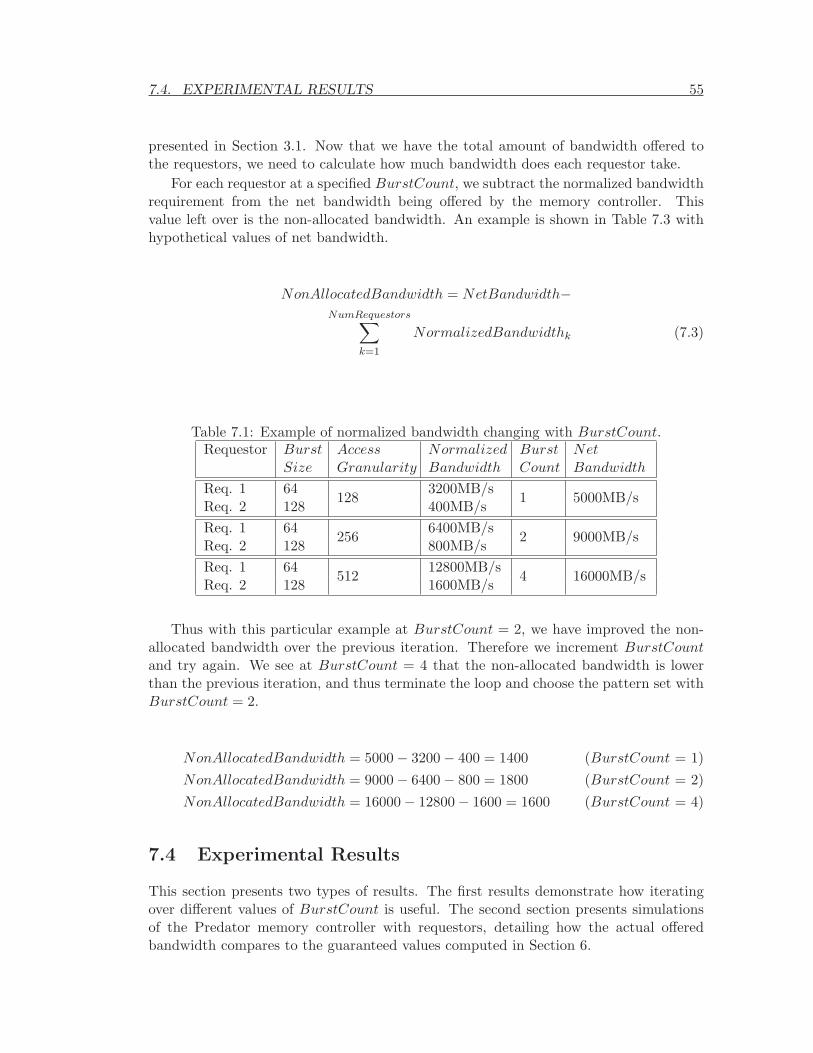
7.4. EXPERIMENTAL RESULTS 55
presented in Section 3.1. Now that we have the total amount of bandwidth offered tothe requestors, we need to calculate how much bandwidth does each requestor take.
For each requestor at a specified BurstCount, we subtract the normalized bandwidthrequirement from the net bandwidth being offered by the memory controller. Thisvalue left over is the non-allocated bandwidth. An example is shown in Table 7.3 withhypothetical values of net bandwidth.
NonAllocatedBandwidth = NetBandwidth−
NumRequestors∑
k=1
NormalizedBandwidthk (7.3)
Table 7.1: Example of normalized bandwidth changing with BurstCount.Requestor Burst
SizeAccessGranularity
NormalizedBandwidth
BurstCount
NetBandwidth
Req. 1 64128
3200MB/s1 5000MB/s
Req. 2 128 400MB/s
Req. 1 64256
6400MB/s2 9000MB/s
Req. 2 128 800MB/s
Req. 1 64512
12800MB/s4 16000MB/s
Req. 2 128 1600MB/s
Thus with this particular example at BurstCount = 2, we have improved the non-allocated bandwidth over the previous iteration. Therefore we increment BurstCountand try again. We see at BurstCount = 4 that the non-allocated bandwidth is lowerthan the previous iteration, and thus terminate the loop and choose the pattern set withBurstCount = 2.
NonAllocatedBandwidth = 5000− 3200− 400 = 1400 (BurstCount = 1)
NonAllocatedBandwidth = 9000− 6400− 800 = 1800 (BurstCount = 2)
NonAllocatedBandwidth = 16000− 12800− 1600 = 1600 (BurstCount = 4)
7.4 Experimental Results
This section presents two types of results. The first results demonstrate how iteratingover different values of BurstCount is useful. The second section presents simulationsof the Predator memory controller with requestors, detailing how the actual offeredbandwidth compares to the guaranteed values computed in Section 6.

56 CHAPTER 7. ALGORITHM CONTEXT
7.4.1 Rates of Satisfaction
The integrated pattern generator iterates over different values of BurstCount to getthe highest rates of latency and bandwidth requirement satisfaction for different usecases. Figures 7.5, 7.6, 7.7, and 7.8 demonstrate the rates of success for meeting a usecase’s bandwidth or latency requirements for fixed BurstCount compared to an iteratingBurstCount.
In each of the following figures, 5000 use cases are used. Each use case has 6 re-questors, and each requestor has randomized requirements based on the following vari-ables. load refers to the percentage of peak bandwidth requested by the requestors.ReqSize is a parameter used to determine the amount of data requested by a requestor.ReqMod is a modifier used in conjunction with ReqSize. The request size of a requestoris determined by randomly selecting a value from 1 to ReqMod, and multiplying it byReqSize. Latency requirements are generated in a similar fashion, with LatReq beinga maximum latency requirement, and LatMod being its modifier. These figures areuseful as they prove that an iterating BurstCount has a higher rate of diverse use caserequirement satisfaction. The values used in the figures are defined in Table 7.2.
Table 7.2: Values of load, request size, and latency requirement.load 82.6%
ReqSize:ReqMod 512:8
LatReq:LatMod 135:100
As seen in Figure 7.5, at a low BurstCount it is difficult to provide enough bandwidthto match the bandwidth requirements of the requestors. Due to the short pattern lengthscreated with a low BurstCount, the priority assigner has more space to work with andthus has an easier task of finding a valid assignment to meet latency requirements. AsBurstCount increases, we see a corresponding increase in bandwidth satisfaction. This isexpected because in the environment that this graph comes from, the request sizes of therequestors are larger than the granularity of the patterns produced for BurstCount 1, 2,and 4. This means that the edata will always be 1, and thus increasing the BurstCountdoes not have a negative effect on bandwidth satisfaction at these values.
Figure 7.6 displays the combined latency and bandwidth satisfaction rate. The com-bined rate of satisfaction is highest with the iterating approach as we predicted in Sec-tion 7, thus verifying that an iterative method provides higher requirement satisfactionover different use cases.
In Figures 7.7 and 7.8, we have decreased ReqSize:ReqMod to 64:8 in order todemonstrate a decrease in bandwidth requirement satisfaction. As seen in Figure 7.7,the bandwidth satisfaction rate drops sharply at BurstCount 4. This occurs because thegranularity of the patterns is now much larger than the request size of the requestors,thus negatively influencing edata as BurstCount increases, and as a result, the bandwidthoffered is reduced.

7.4. EXPERIMENTAL RESULTS 57
0
20
40
60
80
100
120
BC1 BC2 BC4 Iterating
Suc
cess
Rat
e (%
)
Algorithm Type
Bandwidth SatisfiedLatency Satisfied
Figure 7.5: Comparison of fixed BurstCount generator and an iterating generator withlarge request size. The memory specification used is DDR2-400.
0
5
10
15
20
25
30
BC1 BC2 BC4 Iterating
Suc
cess
Rat
e (%
)
Algorithm Type
Latency and Bandwidth Satisfied
Figure 7.6: Comparison of fixed BurstCount generator and an iterating generator withlarge request size. The memory specification used is DDR2-400.
7.4.2 Actual Bandwidth
The results in this section are based on simulations of the Predator memory con-troller with 4 requestors, with a constant backlog of requests. Plotted in Fig-ures 7.9, 7.10, 7.11, and 7.12 are actual measured bandwidth compared against theworst-case bounds guaranteed by the bank scheduling algorithm. In each figure, thesimulation is run twice. In the first simulation, the patterns being executed are forcedto switch from read writes at every opportunity. In the second simulation, switches arenot forced, but allowed to switch at every opportunity. The length of time for all plotsis 16.6 µs. This value was chosen because it is just over the amount of time required toexecute 2 refresh commands. We see at 7.8 µs and at 15.6 µs a small dip in the average

58 CHAPTER 7. ALGORITHM CONTEXT
0
10
20
30
40
50
60
BC1 BC2 BC4 Iterating
Suc
cess
Rat
e (%
)
Algorithm Type
Bandwidth SatisfiedLatency Satisfied
Figure 7.7: Comparison of fixed BurstCount generator and an iterating generator withsmall request size. The memory specification used is DDR2-400.
0
5
10
15
20
25
BC1 BC2 BC4 Iterating
Suc
cess
Rat
e (%
)
Algorithm Type
Latency and Bandwidth Satisfied
Figure 7.8: Comparison of fixed BurstCount generator and an iterating generator withsmall request size. The memory specification used is DDR2-400.
bandwidth due to the refresh pattern executing.As we see in Figure 7.9, the plot of bandwidth when switching is not forced is slightly
higher because the pattern set produced for this memory device is mix dominant. Thismeans that the worst-case scenario in terms of bandwidth offered occurs when there isconstant switching between read and write patterns.
In the remaining figures the forced switch and unforced switch plots are the samebecause the patterns generated for each figure write dominant or mix dominant withswitching patterns of length 0. This implies that the worst-case occurs for forced switch-ing use cases and non-forced switching use cases.

7.4. EXPERIMENTAL RESULTS 59
660
680
700
720
740
760
780
800
0 2 4 6 8 10 12 14 16 18
Net
Ban
dwid
th (
MB
/s)
Time (microseconds)
Actual Bandwidth (Forced Switches)Peak Bandwidth
Worst-Case GuaranteeActual Bandwidth
Figure 7.9: Average bandwidth over time for a DDR2-400 device by simulation.
1100
1200
1300
1400
1500
1600
1700
0 2 4 6 8 10 12 14 16 18
Net
Ban
dwid
th (
MB
/s)
Time (microseconds)
Actual Bandwidth (Forced Switches)Peak Bandwidth
Worst-Case GuaranteeActual Bandwidth
Figure 7.10: Average bandwidth over time for a DDR2-800 device by simulation.

60 CHAPTER 7. ALGORITHM CONTEXT
1000
1100
1200
1300
1400
1500
1600
1700
0 2 4 6 8 10 12 14 16 18
Net
Ban
dwid
th (
MB
/s)
Time (microseconds)
Actual Bandwidth (Forced Switches)Peak Bandwidth
Worst-Case GuaranteeActual Bandwidth
Figure 7.11: Average bandwidth over time for a DDR3-800 device by simulation.
500
1000
1500
2000
2500
3000
0 2 4 6 8 10 12 14 16 18
Net
Ban
dwid
th (
MB
/s)
Time (microseconds)
Actual Bandwidth (Forced Switches)Peak Bandwidth
Worst-Case GuaranteeActual Bandwidth
Figure 7.12: Average bandwidth over time for a DDR3-1600 device by simulation.

Conclusion 8This thesis describes a problem associated with applications being run on real-time sys-tems with hard requirements, namely, the bounding of worst-case latency and bandwidth.It introduces the idea of a hybrid memory controller, Predator, which uses memory pat-terns to interact with an SDRAM device, in order to bound worst-case latency andbandwidth. The problem of creating these memory patterns is described, along with thegoal of this thesis, which is to create a method for producing patterns.
Following this, the thesis describes the architecture and operation of various basiccomponents of the considered platform. These are the SDRAM memory device, andmemory controllers. Current solutions are presented, along with why these solutionsdo not conform to our requests. The Predator memory controller is detailed with moreinformation, and explanations are given on why this controller is suitable.
Basic pattern construction and metrics for evaluating pattern sets are illustrated.The metrics detailed involve memory efficiency, which is an extension of an existingmodel, as well as latency calculations.
Three heuristic-based pattern generation approaches are created. They explore thetrade-offs between run time and net bandwidth offered. Based on experimental results,the bank scheduling algorithm is chosen as it provides a huge decrease in run timecompared to the branch and bound algorithm, while providing much more bandwidththan the ASAP algorithm.
Once the pattern generation algorithm is determined, the generator is integrated intothe design flow of the Predator memory controller. The integration consists of creating aloop between the generator, bandwidth allocator, and priority assigner, such that highestsatisfaction rate of required bandwidth and latency are met. We prove this is the case byrunning the Predator design flow with multiple requestors, and showing that the iteratingBurstCount provides higher satisfaction rates than having a fixed BurstCount.
61

62 CHAPTER 8. CONCLUSION

Future Work 9This section contains ideas for possible future directions of the project.
9.1 3D Stacking
An emerging technology is that of 3D stacking. This technology reduces the cost-per-pinof a package, and therefore allows for some interesting areas of optimization. One theoryto consider would be to have separate buses for reading and writing to a memory device.This could lead to the elimination for the need of switching patterns, and thus increasenet bandwidth offered by mix dominant pattern sets.
A second area of improvement could be in consideration of the memory interface.With reduced cost-per-pin, it could be feasible to widen existing bus widths, or to evenimplement multiple interfaces for a device. These improvements would provide a higherbandwidth to requestors.
9.2 Optimal Pattern Generation
One area for improvement is in the pattern generator. Currently, in the branch andbound algorithm we only search for the shortest access patterns. This idea behind it isthat with shorter access patterns, you increase ebank. However, it has also been shownthat in certain conditions a one or two cycle increase in access pattern length results ina 4 or 5 cycle decrease in the switching patterns. In a case observed experimentally, thepattern set was write dominant, so in fact due to the definition of eswitch the switchingpatterns were irrelevant, thus the shorter access pattern still provided higher bandwidth.But the case remains where the resulting pattern set is mix dominant, in which case theswitching patterns make a difference. Therefore a proposal for making the generatorproduce optimal patterns could be an interesting future direction.
9.3 Low Power Considerations
Currently the generator produces patterns without any consideration for power use. Assuch, interleaving memory map-based patterns are the ideal choice because we are ableto exploit the parallelism of the SDRAM’s bank architecture, and thus provide a highernet bandwidth.
However, this approach also consumes a lot of power as all banks are activated onevery access pattern execution. Activate commands take significantly more power thanthe other SDRAM commands. Therefore, it could be interesting to research how patternconstruction choices could be modified to be aware of power consumption [11].
63

64 CHAPTER 9. FUTURE WORK
9.4 Future SDRAM Iterations
Another area where there may require future improvement is with next generationSDRAM devices. The transition from DDR1 to DDR2 memories saw minor changesin device operation, and the same thing happened again in the transition from DDR2to DDR3. The algorithms detailed above were explicitly designed with those memoriesin mind. It is expected that when DDR4 arrives on the market that in order to fullysupport it some minor revisions must be made to account for new differences in timingconstraints and parameters.

Bibliography
[1] S. Adee. Thanks for the Memories. IEEE Spectrum, 46(5), 2009.
[2] B. Akesson et al. Predator: a predictable SDRAM memory controller. In Proc. CODES+ISSS, 2007.
[3] B. Akesson et al. Real-Time Scheduling Using Credit-Controlled Static-Priority Arbitration. In Proc.RTCSA, Aug. 2008.
[4] N. Audsley. Optimal priority assignment and feasibility of static priority tasks with arbitrary start times.Real-Time Systems, 1991.
[5] S. Dutta et al. Viper: A multiprocessor SOC for advanced set-top box and digital TV systems. IEEE Des.Test. Comput., 2001.
[6] K. Goossens et al. Interconnect and memory organization in SOCs for advanced set-top boxes and TV —Evolution, analysis, and trends. In Interconnect-Centric Design for Advanced SoC and NoC, chapter 15.Kluwer, 2004.
[7] E. Ipek et al. Self-Optimizing Memory Controllers: A Reinforcement Learning Approach. In Intl. Symp.on Computer Architecture (ISCA), 2008.
[8] JEDEC Solid State Technology Association, JEDEC Solid State Technology Association 2004, 2500 WilsonBoulevard, Arlington, VA 22201-3834. DDR3 SDRAM Specification, jesd79-3 proposal edition, Oct 2005.
[9] JEDEC Solid State Technology Association. DDR2 SDRAM Specification, JESD79-2C edition, May 2006.
[10] H. Kopetz and G. Bauer. The time-triggered architecture. Proceedings of the IEEE, 91(1), 2003.
[11] S. Liu et al. A power and temperature aware dram architecture. In DAC ’08: Proceedings of the 45thannual conference on Design automation, 2008.
[12] S. A. McKee. Reflections on the memory wall. In CF ’04: Proceedings of the 1st conference on ComputingFrontiers, 2004.
[13] G. Moore. Progress in digital integrated electronics. In Electron Devices Meeting, volume 21, 1975.
[14] S. Rixner et al. Memory access scheduling. In ISCA ’00: Proceedings of the 27th annual internationalsymposium on Computer architecture, 2000.
[15] J. Shao and B. T. Davis. A burst scheduling access reordering mechanism. In HPCA 13: Symposiumproceedings on High Performance Computer Architecture, 2007.
[16] L. Steffens et al. Real-time analysis for memory access in media processing socs: A practical approach.Proc. ECRTS, 2008.
[17] E. Strooisma. A predictable and composable front-end for system on chip memory controllers. Master’sthesis, Delft University of Technology, May 2008.
[18] L. Woltjer. Optimal DDR controller. Master’s thesis, University of Twente, Jan. 2005.
65

66 BIBLIOGRAPHY

List of relevant DDR timing
constraints and parameters AConstraint Description DDR2-400 Values
(cycles)
tRC Minimum time between successive activate commands to thesame bank
11
tRCD Minimum time between activate and read/write commandson the same bank
3
CL Latency in cycles after a read command until data is avail-able on the bus
3
tWL Latency in cycles after a write command until data is avail-able on the bus
2
tAL Additive latency, used to artificially inflate latency to pro-vide better command bus utilization
0
tRP Minimum time between a precharge command on a bankand a successive activate command
3
tRFC Minimum time between a refresh command and a successiverefresh or activate command
15
tRAS Minimum time after an activate command to a bank untilthat bank is allowed to be precharged
8
tRTP Minimum time between a read and precharge command 2tWR Minimum time after the last data has been written to a bank
until a precharge may be issued3
tFAW Within this time frame at most 4 banks may be activated 8tRRD Minimum time between activates to different banks 2tCCD Used to compute the amount of time needed for a switching
pattern2
tWTR Used to compute the amount of time needed for a switchingpattern
2
BurstSize Number of words produced/consumed per read/write com-mand
Configurable
DataRate Number of words on the data bus per clock cycle 2BurstCount Number of read/write commands per bank per pattern Configurable
67

68 APPENDIX A. LIST OF RELEVANT DDR TIMING CONSTRAINTS AND
PARAMETERS

Glossary BTerm Definition Page
BurstCount Number of read or write commands per bank in amemory pattern
26
BurstSize Number of words per read or write command 10DDR Double Data Rate 7
SDRAM Synchronous Dynamic Random Access Memory 7SoC System-On-Chip 1tread Length of read pattern 26tref Length of refresh pattern 26trtw Length of read to write switching pattern 26
twrite Length of write pattern 26twtr Length of write to read switching patern 26
69

70 APPENDIX B. GLOSSARY
Latency Equation Derivations CFor the case of read dominance,
Θ− tref
1 +trefφ
≥ α ∗ tread
α ≤Θ− tref
(
1 +trefφ
)
∗ tread(C.1)
For the case of write dominance,
Θ− tref
1 +trefφ
≥ α ∗ twrite
α ≤Θ− tref
(
1 +trefφ
)
∗ twrite
(C.2)
For the case of mix read dominance,
Θ− tref
1 +trefφ
≥
⌈
α + 1
2
⌉
∗ twtr +⌈α
2
⌉
∗ tread +⌈α
2
⌉
∗ trtw +⌊α
2
⌋
∗ twrite
Θ− tref
1 +trefφ
≥
(
α + 3
2
)
∗ twtr +
(
α + 2
2
)
∗ tread +
(
α + 2
2
)
∗ trtw +(α
2
)
∗ twrite
Θ− tref
1 +trefφ
≥α ∗ twtr
2+
3 ∗ twtr
2+
α ∗ tread2
+ tread +α ∗ trtw
2+ trtw +
α ∗ twrite
2
Θ− tref
1 +trefφ
−3 ∗ twtr
2− tread − trtw ≥ α ∗
(
twtr
2+
tread2
+trtw2
+twrite
2
)
α ≤
Θ−tref
1+tref
φ
− 3∗twtr
2 − tread − trtw
twtr
2 + tread2 + trtw
2 + twrite
2
(C.3)
71

72 APPENDIX C. LATENCY EQUATION DERIVATIONS
For the case of mix write dominance,
Θ− tref
1 +trefφ
≥
⌈
α + 1
2
⌉
∗ trtw +⌈α
2
⌉
∗ twrite +⌈α
2
⌉
∗ twtr +⌊α
2
⌋
∗ tread
Θ− tref
1 +trefφ
≥
(
α + 3
2
)
∗ trtw +
(
α + 2
2
)
∗ twrite +
(
α + 2
2
)
∗ twtr +(α
2
)
∗ tread
Θ− tref
1 +trefφ
≥α ∗ trtw
2+
3 ∗ trtw2
+α ∗ twrite
2+ twrite +
α ∗ twtr
2+ twtr +
α ∗ tread2
Θ− tref
1 +trefφ
−3 ∗ trtw
2− twrite − twtr ≥ α ∗
(
trtw2
+twrite
2+
twtr
2+
tread2
)
α ≤
Θ−tref
1+tref
φ
− 3∗trtw2 − twrite − twtr
trtw2 + twrite
2 + twtr
2 + tread2
(C.4)

Requestor Specification DThe specification of four requestors are defined below.
<?xml version="1.0" encoding="UTF-8"?>
<!DOCTYPE communication SYSTEM "../../../etc/dtd/communicationgrm.dtd">
<communication>
<application id="Application">
<connection qos="GT" id="0">
<initiator ip="input" port="p1"/>
<target ip="memory_controller" port="p1"/>
<read latency="0" bw="164" burstsize="128"/>
<parameter id="delay" type="bool" value="1"/>
</connection>
<connection qos="GT" id="1">
<initiator ip="filter1" port="p1"/>
<target ip="memory_controller" port="p1"/>
<write latency="0" bw="164" burstsize="128"/>
<parameter id="delay" type="bool" value="1"/>
</connection>
<connection qos="GT" id="2">
<initiator ip="filter1" port="p2"/>
<target ip="memory_controller" port="p1"/>
<read latency="0" bw="164" burstsize="128"/>
<parameter id="delay" type="bool" value="1"/>
</connection>
<connection qos="GT" id="3">
<initiator ip="output" port="p1"/>
<target ip="memory_controller" port="p1"/>
<write latency="0" bw="164" burstsize="128"/>
<parameter id="delay" type="bool" value="1"/>
</connection>
</application>
</communication>
73

74 APPENDIX D. REQUESTOR SPECIFICATION

DDR Memory Specification E<!DOCTYPE architecture SYSTEM "../../../etc/dtd/architecturegrm.dtd">
<architecture id="isss">
...........
...........
<ip id="memory_controller" type="MemoryController">
<port id="p1" type="Target" protocol="MMIO_DTL">
<!-- Memory Specification -->
<parameter id="memoryId" type="string" value="64MB_DDR3-1600_16bit" />
<parameter id="capacity" type="uint" value="65536" />
<parameter id="nbrOfBanks" type="uint" value="4" />
<parameter id="clk" type="uint" value="800" />
<parameter id="dataRate" type="uint" value="2" />
<parameter id="tREFI" type="double" value="7800" />
<parameter id="burstSize" type="uint" value="8" />
<parameter id="wordSize" type="uint" value="2" />
<parameter id="RC" type="uint" value="36" />
<parameter id="RCD" type="uint" value="8" />
<parameter id="CL" type="uint" value="8" />
<parameter id="WL" type="uint" value="7" />
<parameter id="AL" type="uint" value="0" />
<parameter id="RP" type="uint" value="8" />
<parameter id="RFC" type="uint" value="72" />
<parameter id="RAS" type="uint" value="28" />
<parameter id="RTP" type="uint" value="6" />
<parameter id="WR" type="uint" value="12" />
<parameter id="FAW4" type="uint" value="24" />
<parameter id="RRD" type="uint" value="5" />
<parameter id="CCD" type="uint" value="4" />
<parameter id="WTR" type="uint" value="6" />
..........
..........
</port>
</ip>
</architecture>
75