endpoint detection of low open area contact etches from … · contact etches from optical emission...
TRANSCRIPT

AEC/APC 2000
Endpoint Detection of Low Open Area Contact Etches from Optical Emission
Spectroscopy Measurements
Kevin Benson, Verity Instruments, Inc.Francis Celii, Texas Instruments, Inc.
Kenneth C. Harvey, Verity Instruments, Inc.* Jimmy W. Hosch, Verity Instruments, Inc.
* Presenter

AEC/APC 2000
Agenda
• Goals of the project
• Hardware and data collection methods
• Calibration of the analysis algorithm
• Endpoint results on graded % open area contacts
• Conclusion

AEC/APC 2000
Projects Goals
• Demonstrate OES endpoint on low open area contact etch
• Accommodate plasma spectral intensity modulation caused by rotating magnetic fields
• Develop an endpoint detection algorithm that shortens the time and spectroscopy expertise that is required for a new etch process

AEC/APC 2000
Approach
• Use a spectrograph to measure plasma light intensities (200-800 nm)
• Synchronize the data collection with the rotating magnet
• Apply multivariate analysis methods to take full advantage of the wealth of spectral data

AEC/APC 2000
TEL DRM Etcher
PlasmaBottom Electrode
Tomonochromatoror spectrometer
Top Electrode
Collimating/Focusing Optics
~ 13.56 MHz
Gas Feed
PermanentMagnets

AEC/APC 2000
Synchronized Data Collection
SD1024Spectrograph
Hall-Effect Sensor
Control Box
Hall-EffectSensor
RotatingMagnet
EtchChamber
#2“RF-On” Signal canreplace the “Start/Stop”Toggle Switch
EtchChamber
#1
“Start/Stop” Toggle Switch
TELFiberOptic
Lap-Top
TEL Magnet RotationSensor can ReplaceH-E Sensor
Integration Time = 100 msec.28 Spectra/Magnet Rotation
TEL DRM Etcher
AEC/APC 2000
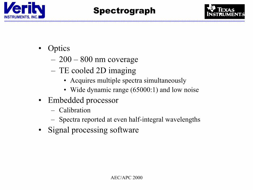
Spectrograph
• Optics– 200 – 800 nm coverage– TE cooled 2D imaging
• Acquires multiple spectra simultaneously• Wide dynamic range (65000:1) and low noise
• Embedded processor– Calibration– Spectra reported at even half-integral wavelengths
• Signal processing software

AEC/APC 2000
Plasma Spectrum
Typical Measured Spectrum

AEC/APC 2000
Plasma Spectrum
Time variation of signal at 325 nm Close up

AEC/APC 2000
Plasma Spectrum
Time variation of signal at 325 nm Variation of spectrum,at Sample 409 and 419
AEC/APC 2000
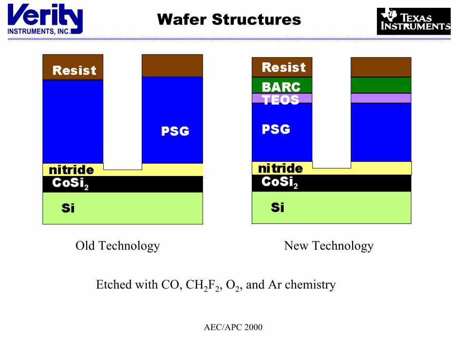
Wafer Structures
Old Technology New Technology
Etched with CO, CH2F2, O2, and Ar chemistry
AEC/APC 2000
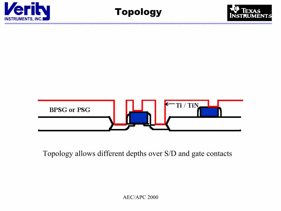
Topology
Topology allows different depths over S/D and gate contacts
AEC/APC 2000
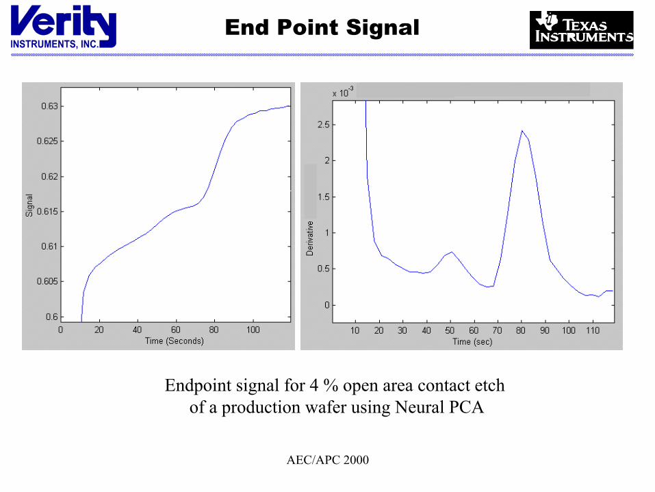
End Point Signal
Endpoint signal for 4 % open area contact etchof a production wafer using Neural PCA
AEC/APC 2000
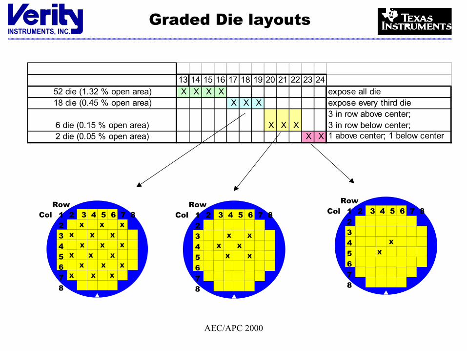
Graded Die layouts
Row12345678
Col 2 3 4 5 6 7 8
X
X
X
X X
X
Row12345678
Col 2 3 4 5 6 7 8
X
X
Row12345678
Col 2 3 4 5 6 7 8
X
X
X
X X
XX
X
XX
X
X
X X
X X X
X
13 14 15 16 17 18 19 20 21 22 23 2452 die (1.32 % open area) X X X X expose all die18 die (0.45 % open area) X X X expose every third die
6 die (0.15 % open area) X X X3 in row above center; 3 in row below center;
2 die (0.05 % open area) X X 1 above center; 1 below center
AEC/APC 2000
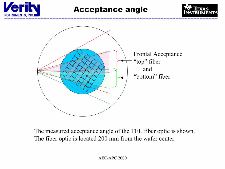
Acceptance angle
The measured acceptance angle of the TEL fiber optic is shown.The fiber optic is located 200 mm from the wafer center.
Frontal Acceptance“top” fiber
and“bottom” fiber
AEC/APC 2000
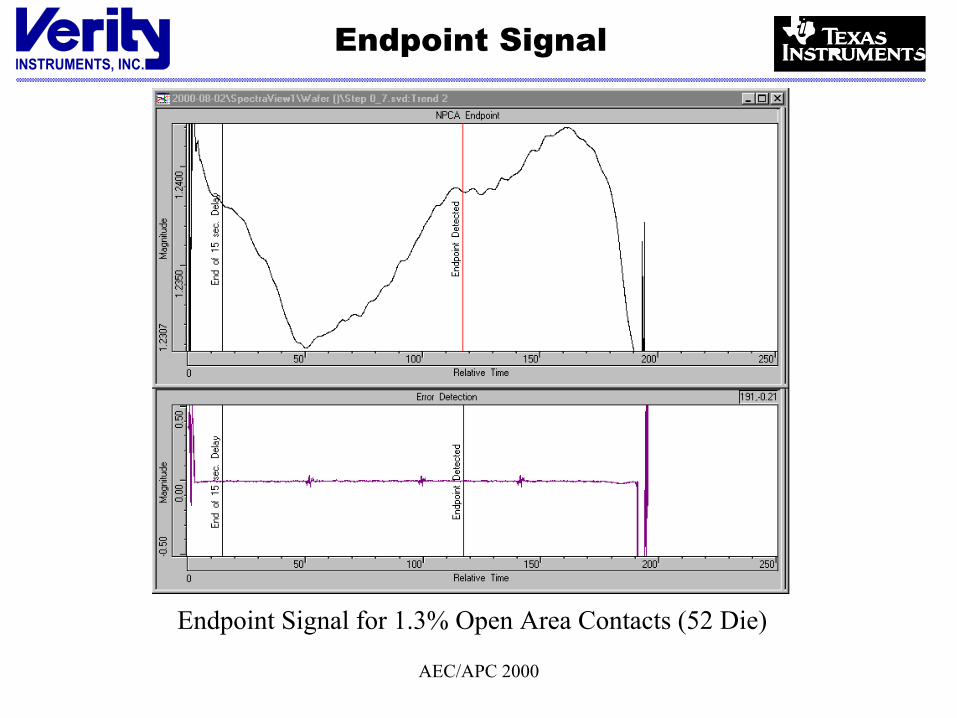
Endpoint Signal
Endpoint Signal for 1.3% Open Area Contacts (52 Die)
AEC/APC 2000
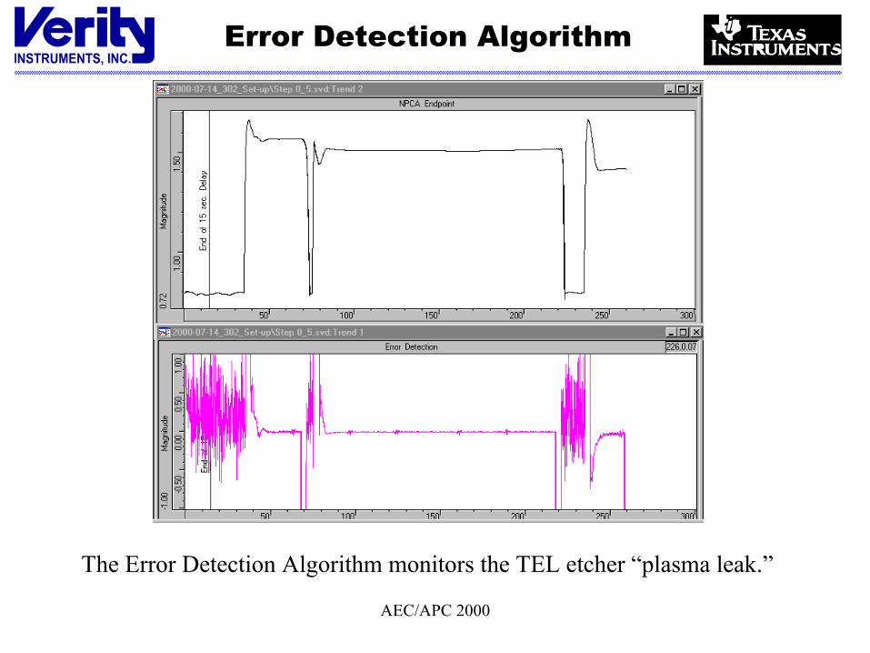
Error Detection Algorithm
The Error Detection Algorithm monitors the TEL etcher “plasma leak.”
AEC/APC 2000
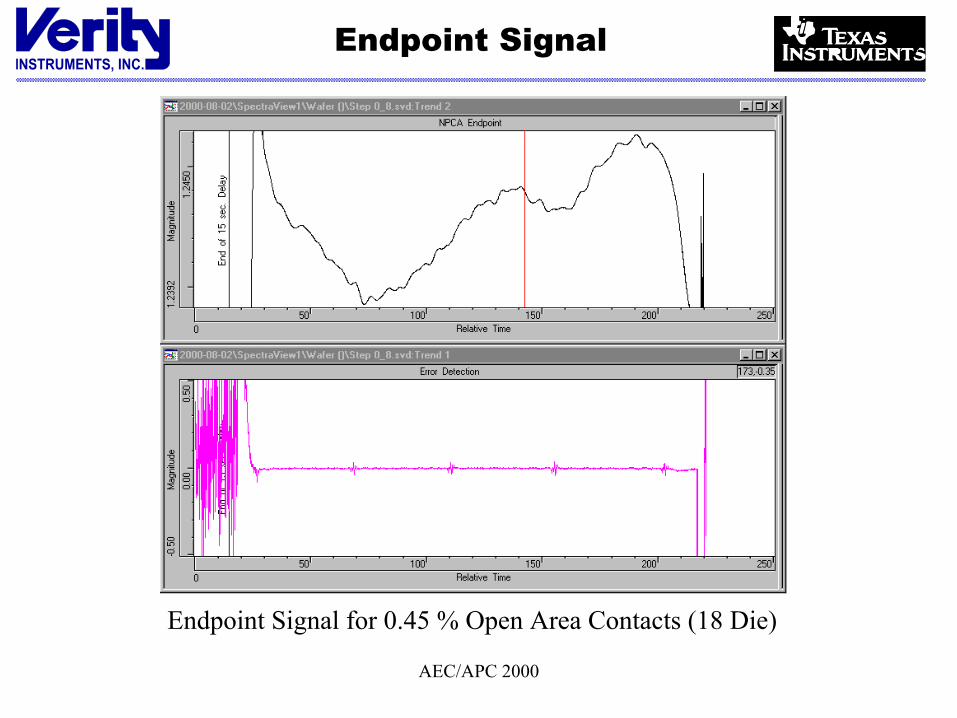
Endpoint Signal
Endpoint Signal for 0.45 % Open Area Contacts (18 Die)

AEC/APC 2000
Endpoint Signal
Endpoint Signal for 0.15 % Open Area Contacts (6 Die)

AEC/APC 2000
Endpoint Signal
Endpoint Signal for 0.05 % Open Area Contacts (2 Die)

AEC/APC 2000
Endpoint Times
Wafer # % Open Area Endpoint (sec.)
13 1.3 124
17 0.4 126
20 0.1 121
23 0.05 124

AEC/APC 2000
Endpoint Trace
Endpoint Trace for 100% Open Area Contacts (blanket wafer)
AEC/APC 2000
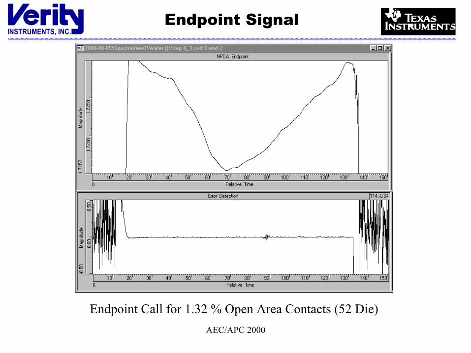
Endpoint Signal
Endpoint Call for 1.32 % Open Area Contacts (52 Die)

AEC/APC 2000
Endpoint Signal
Endpoint Call for 0.45 % Open Area Contacts (18 Die)

AEC/APC 2000
Endpoint Signal
Endpoint Call for 0.15 % Open Area Contacts (6 Die)
AEC/APC 2000
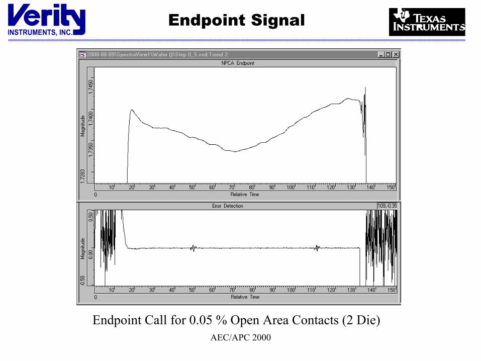
Endpoint Signal
Endpoint Call for 0.05 % Open Area Contacts (2 Die)

AEC/APC 2000
Endpoint Call Times
Wafer # % Open Area Endpoint (sec.)
15 1.3 121
18 0.4 124
21 0.1 122
24 0.05 122

AEC/APC 2000
X-SEM Results
Square contacts Rectangular contacts

AEC/APC 2000
X-SEM Results
Square contacts Rectangular contacts

AEC/APC 2000
Summary
• Contact etch endpoint can be detected well below 0.1 % open area with OES.
• Plasma spectral intensity modulation can be accommodated by synchronizing data collection with magnet rotation.
• Multivariate analysis takes advantage of the wealth of data from the spectrograph to enhance the endpoint signal-to-noise.