esa-estec gstp - analog silicon compiler for mixed...
TRANSCRIPT

ESA-ESTEC GSTP - Analog SiliconCompiler for Mixed-Signal ASICs
Analog Module Generator Software -AMGIE & MONDRIAAN

Final presentation – ESA-ESTEC 7/3/2001 Geert Van der Plas 2
Outlinel Introductionl Objectives of WP1100 & WP1300l AMGIEl Hierarchical Cell Design in AMGIEl Low Power Optimization in AMGIEl Radiation Tolerant Designl Yield Optimizationl Mondriaanl Conclusions

Final presentation – ESA-ESTEC 7/3/2001 Geert Van der Plas 3
Introductionl Software development: WP1100 & WP1300l WP1100: Tool Requirement Analysis
m ASICs/GVdP/WP1 report
l WP1300: Software Implementation & Verificationm Updated AMGIE softwarem Mondriaan toolsetm Software User Manual

Final presentation – ESA-ESTEC 7/3/2001 Geert Van der Plas 4
Objectivesl ASTP4 project: Analog Module Generator (AMG)
m Targeted to OPAMP level circuits :automatic synthesis from specifications to layout
m Both for novice and experienced designers
l Extend and improve Analog Module Generatorl Reorient for expert designers
m High-performance circuits: high-speed A/D converterm Toolbox approach
l Radiation tolerancem CSA-PSA circuit

Final presentation – ESA-ESTEC 7/3/2001 Geert Van der Plas 5
Objectives cont’dl Translate Objectives into Requirementsl Tool Requirement Analysis (ASICs/GVdP/WP1)
m Hierarchical cell design in AMGIEm Low power optimization in AMGIEm Radiation tolerant designm Yield optimizationm Mondriaan

Final presentation – ESA-ESTEC 7/3/2001 Geert Van der Plas 6
Outlinel Introductionl Objectives of WP1100 & WP1300l AMGIEl Hierarchical Cell Design in AMGIEl Low Power Optimization in AMGIEl Radiation Tolerant Designl Yield Optimizationl Mondriaanl Conclusions

Final presentation – ESA-ESTEC 7/3/2001 Geert Van der Plas 7
AMGIE: DefinitionsBehaviour
Specifications
Structure
Sizes & Biasing
TopologySelection
Sizing
LayoutGeneration
+
-
L1=1uIB=10uA
W1=10u
Vout := A(V+ - V-)
Av0 > 60dBGBW > 1 MHz ...
+constraint specifications :
Schematic synthesis
Geometry
W2=12u L2=1uL3=2u
Layout
W3=18u

Final presentation – ESA-ESTEC 7/3/2001 Geert Van der Plas 8
AMGIEl Synthesis of OPAMP level complexity circuitsl Design methodology
m Performance drivenm Hierarchicalm Design stylesnFull customnFixed
l Cell Librarym Custom topologiesm Fixed cellsnManualnSynthesized

Final presentation – ESA-ESTEC 7/3/2001 Geert Van der Plas 9
Outlinel Introductionl Objectives of WP1100 & WP1300l AMGIEl Hierarchical Cell Design in AMGIEl Low Power Optimization in AMGIEl Radiation Tolerant Designl Yield Optimizationl Mondriaanl Conclusions

Final presentation – ESA-ESTEC 7/3/2001 Geert Van der Plas 10
Hierarchical Cell Design in AMGIEl Implementation of stubsl Design Controllerl Sizing & Optimization tool] Specification Translation tool
l Layout tool] Layout Assembly tool

Final presentation – ESA-ESTEC 7/3/2001 Geert Van der Plas 11
AMGIE: Design Flowl Top downl Bottom up
cationVerifi-
cationVerifi-
Specifications at Level i + 1
TopologySelection
Sizing andOptimization
Extraction
LayoutGeneration
Layout at Level i + 1
Specifications at Level i Layout at Level i
Red
esig
n
Level i + 1
Level i

Final presentation – ESA-ESTEC 7/3/2001 Geert Van der Plas 12
Design Controller
Old Design Flow(ASTP4 AMG) New Design Flow
(GSTP AMGIE)

Final presentation – ESA-ESTEC 7/3/2001 Geert Van der Plas 13
Hierarchical Cell Design: Sizing Tooll AMGIE sizing & optimization tool
m Sizes of devicesm Biasing of devices
l Hierarchicalm Sizes of devicesm Biasing of devicesm Specifications of subcells[Specification translation
l S&O toolm Modified data handling

Final presentation – ESA-ESTEC 7/3/2001 Geert Van der Plas 14
Hierarchical Cell Design: Layout Tooll LAYLA [Lampaert ‘99]
m Analog place & routem Direct performance driven, analog constraintsnSymmetrynMatchingnParasitics
m Optimized for typical analog circuitsnOTAnOpampnComparatorn…
Final presentation – ESA-ESTEC 7/3/2001 Geert Van der Plas 15
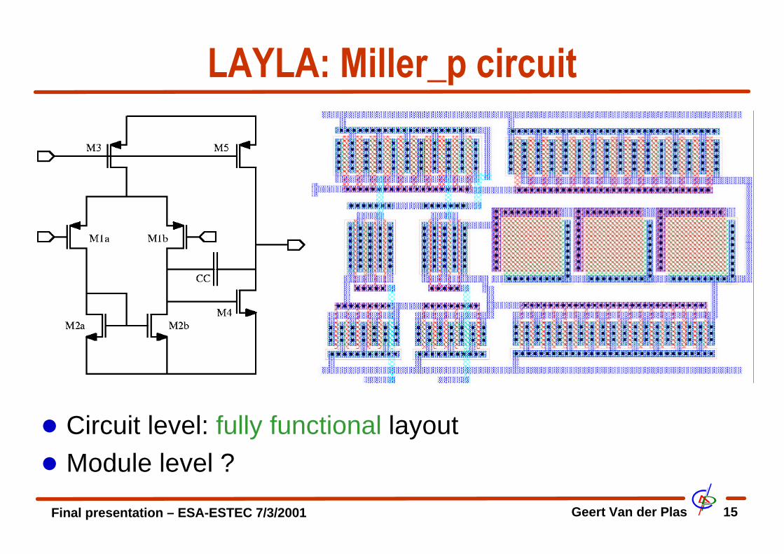
LAYLA: Miller_p circuit
l Circuit level: fully functional layoutl Module level ?

Final presentation – ESA-ESTEC 7/3/2001 Geert Van der Plas 16
Module Placement & Routing

Final presentation – ESA-ESTEC 7/3/2001 Geert Van der Plas 17
Improved LAYLAl External Cellsl Floorplanning with soft cellsl Circuits & Modules:
m OTAsm Comparatorsm CSA, PSAm CSA-PSA Modulem A/D & D/A ?
] Mondriaan

Final presentation – ESA-ESTEC 7/3/2001 Geert Van der Plas 18
Outlinel Introductionl Objectives of WP1100 & WP1300l AMGIEl Hierarchical Cell Design in AMGIEl Low Power Optimization in AMGIEl Radiation Tolerant Designl Yield Optimizationl Mondriaanl Conclusions

Final presentation – ESA-ESTEC 7/3/2001 Geert Van der Plas 19
Low Power Optimization: Probleml Optimization algorithms
m Global: Simulated Annealingm Local: Hooke-Jeeves_ highly constrained problems
l Optimization processm Black boxm Only cost trace is visiblem Final result can be investigatedm How to find good cost function parameters ?

Final presentation – ESA-ESTEC 7/3/2001 Geert Van der Plas 20
Low Power Optimization: SQPl Added gradient based optimization algorithm
m Sequential Quadratic Programming (SQP)m Active constraint set
Buffer

Final presentation – ESA-ESTEC 7/3/2001 Geert Van der Plas 21
Example: Power-Area Tradeoff
Final presentation – ESA-ESTEC 7/3/2001 Geert Van der Plas 22
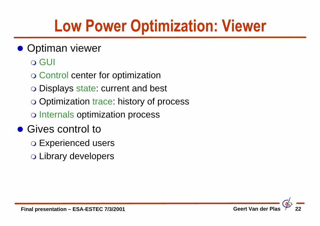
Low Power Optimization: Viewerl Optiman viewer
m GUIm Control center for optimizationm Displays state: current and bestm Optimization trace: history of processm Internals optimization process
l Gives control tom Experienced usersm Library developers

Final presentation – ESA-ESTEC 7/3/2001 Geert Van der Plas 23

Final presentation – ESA-ESTEC 7/3/2001 Geert Van der Plas 24
Outlinel Introductionl Objectives of WP1100 & WP1300l AMGIEl Hierarchical Cell Design in AMGIEl Low Power Optimization in AMGIEl Radiation Tolerant Designl Yield Optimizationl Mondriaanl Conclusions

Final presentation – ESA-ESTEC 7/3/2001 Geert Van der Plas 25
Radiation Tolerant Designl Problem description
M1
P1
P1
M1
P1
n NMOS
VT

Final presentation – ESA-ESTEC 7/3/2001 Geert Van der Plas 26
Radiation Tolerant Designl Counter irradiation effects by design
m Layout measuresm Adapt sizing models: W & L, parasitics
l Verify designm Commercial simulatorm Irradiation parameters

Final presentation – ESA-ESTEC 7/3/2001 Geert Van der Plas 27
Edgeless Device – Gate All Aroundl Avoid the leakage path !
Source
Gate
Drain
?
?
eff
eff
L
W

Final presentation – ESA-ESTEC 7/3/2001 Geert Van der Plas 28
Gate All Around DeviceDrain
Gate
Source
W1
W2
L
x x+dx
=
=
eff
eff
eff
eff
LWW
W
WWL
W
8exp
)ln(
8
1
2
1
2

Final presentation – ESA-ESTEC 7/3/2001 Geert Van der Plas 29
Device Generator
CADENCE
&
LAYLA

Final presentation – ESA-ESTEC 7/3/2001 Geert Van der Plas 30
Radiation Tolerant Design: Sizingl Margins
m VT Shiftsm Leakage currents
l Gate all around devicem Use geometric modelm W & Lm Parasitics: AS, AD, PS, PD, NRS, NRD, …

Final presentation – ESA-ESTEC 7/3/2001 Geert Van der Plas 31
KULeuven PDFE Example
1.1mm
550u
m
Rf CSA Diff INT
GAA

Final presentation – ESA-ESTEC 7/3/2001 Geert Van der Plas 32
Radiation Tolerant Design: Verificationl Verification
m Commercial simulators offer simulation of irradiation effectsm Hspice has been integrated in the verification toolm 2 examples:nNMOS transistornSimulated KULeuven PDFE

Final presentation – ESA-ESTEC 7/3/2001 Geert Van der Plas 33
NMOS Transistor: Subthreshold Slope

Final presentation – ESA-ESTEC 7/3/2001 Geert Van der Plas 34

Final presentation – ESA-ESTEC 7/3/2001 Geert Van der Plas 35
Outlinel Introductionl Objectives of WP1100 & WP1300l AMGIEl Hierarchical Cell Design in AMGIEl Low Power Optimization in AMGIEl Radiation Tolerant Designl Yield Optimizationl Mondriaanl Conclusions

Final presentation – ESA-ESTEC 7/3/2001 Geert Van der Plas 36
Yield: Problem Descriptionl Nominal Designl Manufacturing tolerance
m Inter-dienWafer batchesnDifferent wafers in one batchnModeled through spice parameter 6σ intervals
m Intra-dienSame devices, unequal parametersnMismatch
l Yieldm Some circuits are not within spec
Final presentation – ESA-ESTEC 7/3/2001 Geert Van der Plas 37
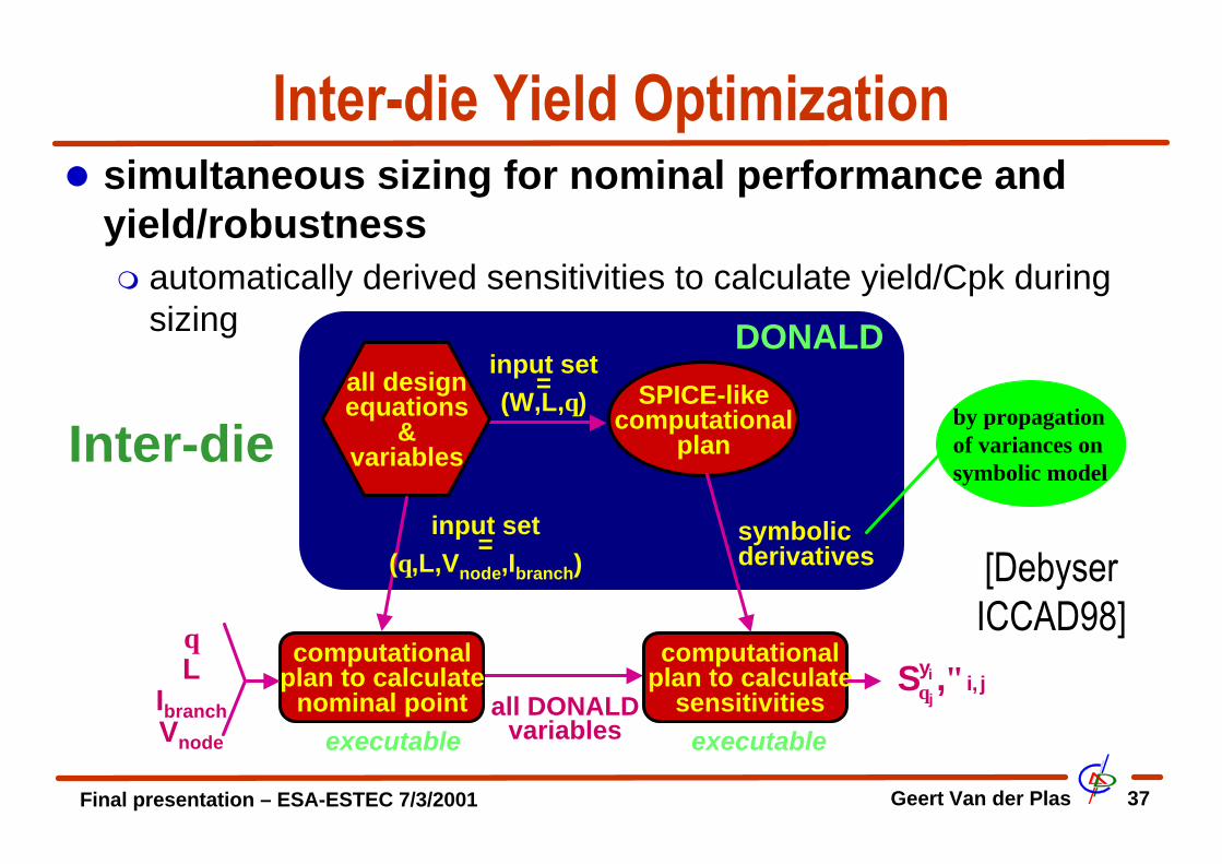
Inter-die Yield Optimizationl simultaneous sizing for nominal performance and
yield/robustnessm automatically derived sensitivities to calculate yield/Cpk during
sizing
computationalplan to calculate
nominal point
all designequations
&variables
SPICE-likecomputational
plan
computationalplan to calculate
sensitivities
input set=
(W,L,θ)
DONALD
input set=
(θ,L,Vnode,Ibranch)symbolicderivatives
all DONALDvariables
θL
IbranchVnode
j,iy ,S i
j∀θ
executable executable
by propagationof variances onsymbolic model
Inter-die
[DebyserICCAD98]

Final presentation – ESA-ESTEC 7/3/2001 Geert Van der Plas 38
Inter-die Yield Optimization: Example
Monte Carlo
mexample : current-buffer OTAn random starting pointnnominal/yield/Cpk optimizationnMonte-Carlo verification
results after optimization
GBW>100MHzAv0>60dB
PM>60degOR>3.0VVoff<5mVItot<3.0mA
16578.060.23.14.82.6
17278.163.63.273.52.6
23.11.680.20.050.140.4
21.41.740.4
0.0580.7
0.56
y yyσ yσyield model
specs
CPU times
Monte Carloyield modeloptimization
2h20’ (300s)10”
2h15’
Μ1a Μ1b
Μ7
Μ6
CL
Μ3b
Μ2bΜ2a
Μ3a
Μ5a
Μ4a
Μ5b
Μ4bVbias1
Vbias2
Vbias3
V+ V- Vout

Final presentation – ESA-ESTEC 7/3/2001 Geert Van der Plas 39
Example: Results
1 2
• 1 : pdf distributions without yield/Cpk(nominal only)
• 2 : pdf distributions with yield/Cpk(nominal + yield)
Final presentation – ESA-ESTEC 7/3/2001 Geert Van der Plas 40
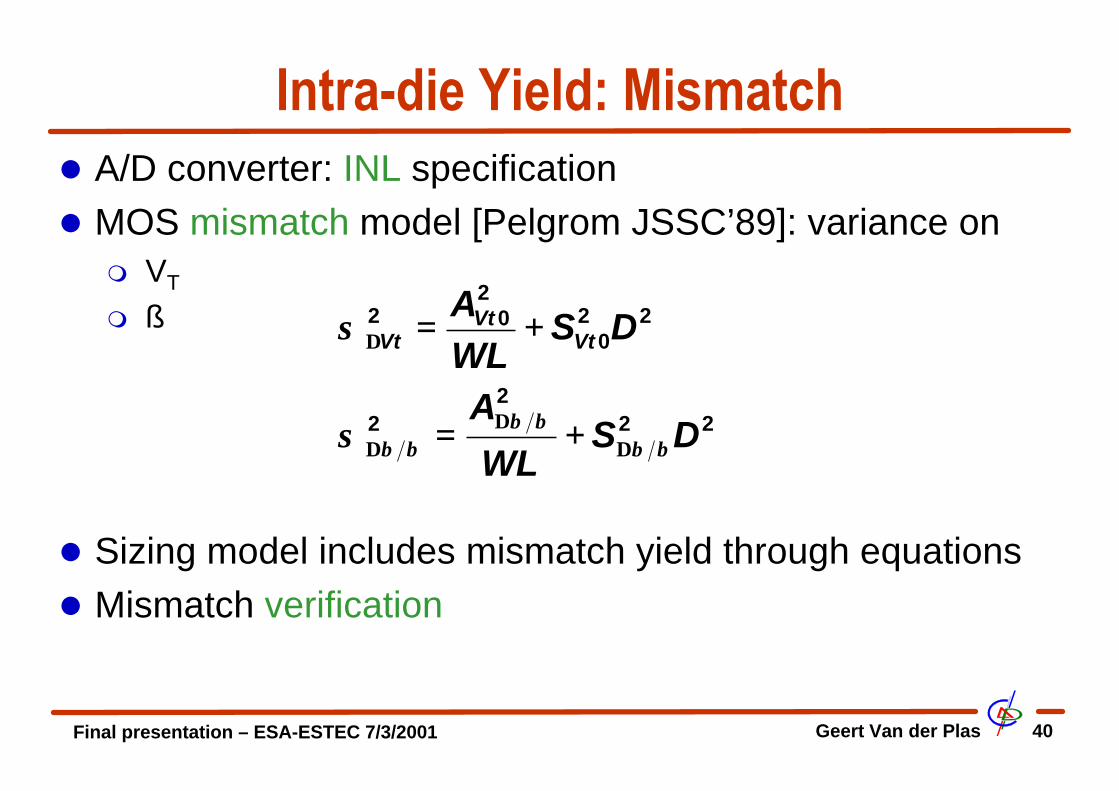
Intra-die Yield: Mismatchl A/D converter: INL specificationl MOS mismatch model [Pelgrom JSSC’89]: variance on
m VT
m ß
l Sizing model includes mismatch yield through equationsl Mismatch verification
222
2
220
202
DSWL
A
DSWLA
VtVt
Vt
ββββ
ββσ
σ
∆∆
∆
∆
+=
+=

Final presentation – ESA-ESTEC 7/3/2001 Geert Van der Plas 41
Mismatch verification: Comparator
vin+ vin-
vout+ vout-
φ1
φ2
φ1
φ1φ1
M4a M4b
M2a M2b
M3a M3b
Mbias
M5a M5b
M1a M1b

Final presentation – ESA-ESTEC 7/3/2001 Geert Van der Plas 42
Transient Simulation
t0
∆Vout
t0
t1t2
output voltage at a fixed time point
[VdPlas ICECS99]

Final presentation – ESA-ESTEC 7/3/2001 Geert Van der Plas 43
Result Monte Carlo Simulation

Final presentation – ESA-ESTEC 7/3/2001 Geert Van der Plas 44
Outlinel Introductionl Objectives of WP1100 & WP1300l AMGIEl Hierarchical Cell Design in AMGIEl Low Power Optimization in AMGIEl Radiation Tolerant Designl Yield Optimizationl Mondriaanl Conclusions

Final presentation – ESA-ESTEC 7/3/2001 Geert Van der Plas 45
Mondriaan: Introductionl Often used analog signal processing architectures:
generation, propagation, multiplication
# output # output # output
# input
1 A B C
1 A B C
1 A B C
1 A B C
# input[VdPlas CICC98]

Final presentation – ESA-ESTEC 7/3/2001 Geert Van der Plas 46
Examples
A/D converter D/A converter

Final presentation – ESA-ESTEC 7/3/2001 Geert Van der Plas 47
Generation of Regular Layout Structuresl Hierarchy
L changes lead to a complete redesign of the cell hierarchyL exceptions difficult to handle
l Stretch & Tile [Neff]☺ extremely fast generationL all connectivity by abutmentL large setup time

Final presentation – ESA-ESTEC 7/3/2001 Geert Van der Plas 48
Mondriaan Featuresl Regular array of cellsl Use abutment for power, biasing, …l Bus & Channel routing for extra connectivity
m Y bus routing connects to cellsm X channel routing connects to Y routing
l Mondriaan Flowl Bus and Tree device generators

Final presentation – ESA-ESTEC 7/3/2001 Geert Van der Plas 49
Mondriaan: Layout Modell Matrix of master cells (master1,master2,...)l Optional column spacer cells (sp1, sp2)
sp1
sp1 master1 sp2
master2
master3
sp1sp1

Final presentation – ESA-ESTEC 7/3/2001 Geert Van der Plas 50
Mondriaan: Layout Modell Symbolic view: X & Y channel routing
contactarea
YX-Y

Final presentation – ESA-ESTEC 7/3/2001 Geert Van der Plas 51
Mondriaan Flow

Final presentation – ESA-ESTEC 7/3/2001 Geert Van der Plas 52
Example: 4-bit Current Source Arrayl 1 current source == 4 MOS transistorsl symmetric placementl Floorplan
1A2A0A3A5A4A
7A6A
9A8A
10A11A12A13A14A--
2B1B0B
0C1C 2C
0D1D2D
== 3B8B7B
12B13B14B
11B9B 10B
--5B 4B6B
3C
12C
14C13C
--
11C
5C 4C6C
8C9C
7C
10C
6D
8D9D
7D3D
12D
14D13D
10D11D
-- 5D4Ddummies
j
jA
jB
jC
jD
dummies
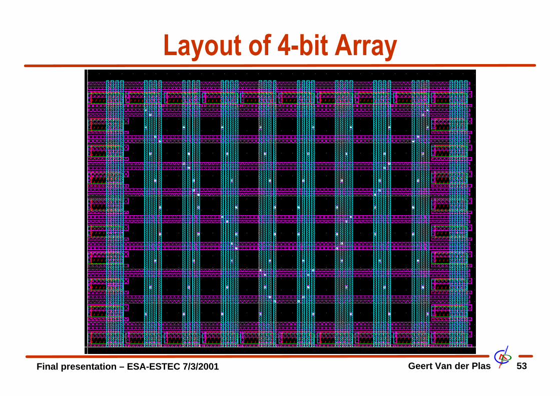
Final presentation – ESA-ESTEC 7/3/2001 Geert Van der Plas 53
Layout of 4-bit Array
Final presentation – ESA-ESTEC 7/3/2001 Geert Van der Plas 54
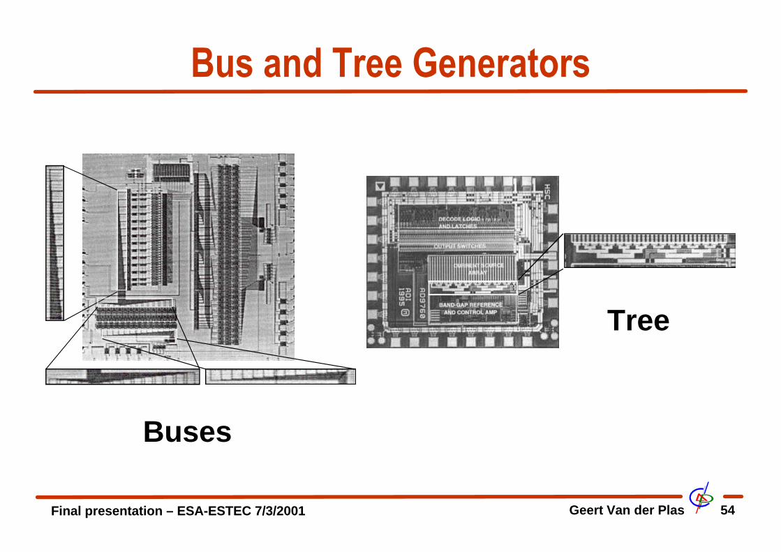
Bus and Tree Generators
Tree
Buses

Final presentation – ESA-ESTEC 7/3/2001 Geert Van der Plas 55
Bus Generatorsl N-to-N connections: 6 typesl Signal distribution, clock distribution, …
(a) (b)
(c)
routing2
via
routing1routing2
via
routing1
(d) (e)
(f)

Final presentation – ESA-ESTEC 7/3/2001 Geert Van der Plas 56
Tree Generatorsl 1-to-N connections: 3 typesl Clock distribution, biasing, power, ground, …
pitchwidth
height
growstep=2startwidth
routing layer1 routing layer2 via layer
pitch width
height
grow-ratio
width pitch
height
pitch2
Final presentation – ESA-ESTEC 7/3/2001 Geert Van der Plas 57
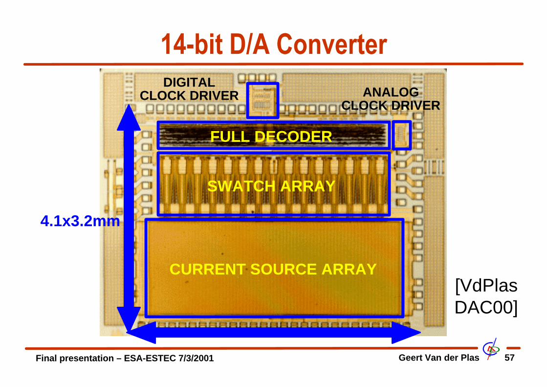
CURRENT SOURCE ARRAY
SWATCH ARRAY
FULL DECODER
DIGITALCLOCK DRIVER ANALOG
CLOCK DRIVER
4.1x3.2mm
14-bit D/A Converter
[VdPlasDAC00]
Final presentation – ESA-ESTEC 7/3/2001 Geert Van der Plas 58
Outlinel Introductionl Objectives of WP1100 & WP1300l AMGIEl Hierarchical Cell Design in AMGIEl Low Power Optimization in AMGIEl Radiation Tolerant Designl Yield Optimizationl Mondriaanl Conclusions

Final presentation – ESA-ESTEC 7/3/2001 Geert Van der Plas 59
Conclusionsl Improved AMGIE
m Hierarchical cell designm Low power optimizationm Yield optimization
l Radiation tolerancem GAAm Verification
l Mondriaanm Layout for A/D converters

Final presentation – ESA-ESTEC 7/3/2001 Geert Van der Plas 60
Publicationsl G. Van der Plas, J. Vandenbussche, G. Gielen and W. Sansen, "Mondriaan: a
Tool for Automated Layout Synthesis of Array-type Analog Blocks", Proc. on theIEEE 1998 Custom Integrated Circuits Conference (CICC), pp. 485-488,California, May 1998.
l G. Debyser, G. Gielen, “Efficient analog circuit synthesis with simultaneous yieldand robustness optimization”, proceedings ACM/IEEE International Conferenceon Computer-Aided Design (ICCAD), pp. 308-311, November 1998.
l G. Van der Plas, J. Vandenbussche, W. Verhaegen, G. Gielen and W.Sansen,"Statistical Behavioral Modeling for A/D Converters", IEEE 1999 InternationalConference on Electronics, Circuits and Systems (ICECS), pp. 1713-1716,Cyprus, September 1999.
l G. Van der Plas, J. Vandenbussche, W. Daems, A. Van Den Bosch, G. Gielen, M.Steyaert, W. Sansen, "Systematic design of a 14-bit 150-MS/s CMOS Current-Steering D/A Converter", in Design Automation Conference (DAC), pp. 452-457,Los Angelos, USA, June 5-9, 2000.