experiences with decapsulation of copper bond wire devices ... · 13.06.2016 · • literature...
TRANSCRIPT

Experiences with Decapsulation of Copper Bond Wire Devices using
Laser Ablation Presented By: Trevor A. Devaney
Presented to: NEPPJune 13, 2016

History- How’d we get here?• Back in 2013 we had a NASA Program subcontractor
using Plastic Encapsulated parts that we were performing DPA for when…..
2
Hey, where’d the wires go???

History- How’d we get here?
3
• Up to that point, we had never seen wires made of anything but Gold or Aluminum at DPA or FA.
• We had traditionally performed Acid Decapsulation by hand and had never really run into too much trouble.
• We had heard some commercial manufacturers were looking at copper wire bonding to save money due to the increases in the Gold price. They are saving less than a tenth of a percent per part……

History- How’d we get here?
4
• How do you decapsulate Copper Wire Bonded Parts??
• We had heard that you don’t rinse the part until decapsulation is complete or else the passivation on the copper wires breaks down and washes away with each rinse cycle. This was successful at the time.
However, this does not expose the lead frame stitch bonds for evaluation. Note also, the copper metallization on the Die surface that had been removedWith the wires previously.

• We also encountered Microcircuits that had nickel plated copper metallized bond pads instead of just aluminum.
5
History- How’d we get here?
New Rule- Always cross-section before Decapsulation to know what you are in for! X-Ray can also give clues- lead frame density is close to copper wire density, whereas gold is higher density.

• Even wire diameter is critical. Smaller wire diameters (< 1.25 mils) do not suffer decapsulation as well.
6
History- How’d we get here?

7
• Immediately following the onset of Copper Wire Bonded Devices, we looked at and procured a Nisene Copper Protect Jet Etcher. That seemed to take the guess work out of the process as far as exposing the die and die bonds, however, it did not expose the stitch bonds at the post. Following Mil-Std-1580B at the time, this was not a requirement for Au wires (No mention of Cu).
• We were becoming aware of new failure modes occurring at the stitch bonds due to moisture ingress.
• Missile and Terrestrial Military users were less than confident in the stitch bonds due to the lack of reliability data provided by the manufacturers.
History- How’d we get here?

88
History- How’d we get here?Here we are… We can expose the die bonds, But now we want to expose the post bonds too.
Unfortunately, jet etching or etching by hand with acids tends to remove the material in the center (over the die) faster than the periphery even with a maximum sized template or mechanically prepped area.
The longer the die area is exposed to the acids while attempting to expose the post bonds (which are often lower than the die plane) the greater the damage to those wires.

9
We had to try something new…
• Literature concerning decapsulation of Copper wire bonds suggested that Laser Ablation of the plastic encapsulation was the way to go.
• The most useful paper was one written by Jake Klein and Lucas Copeland from T.I. in 2010 titled “Decapsulation of Copper Bonded Plastic Encapsulated Integrated Circuits Utilizing Laser Ablation and Mixed Acid Chemistry” which was presented at ITSFA.
• The approach presented was to ablate as much plastic away as possible from the Die and Wires to allow for a fast acid etch of the remaining plastic material.
• However, the laser could not be allowed to hit the die surface or damage could occur.

1010
We had to try something new…• We had a project requiring full exposure of all the
wires from a large quantity of FPGA samples.
• To make it more challenging, there where two heights of bond wires (upper and lower).
• We had to try Laser Ablation- We had EAG in the Bay area use their CLC Laser followed by an acid application and this showed great promise.
• We knew this was the approach to follow and ordered our own unit, an F/A Cube from CLC.

11
Laser Application Video

Laser Ablation Application
• Using an X-ray overlaid on the device image, you determine the size of lead frame and establish the area/grid to ablate.
• Apply Laser in a raster mode and ablate the plastic down to a point just above the top of the ball bonds on the Die (3-8 mils from Die Surface). You will expose the wire loops. Be sure to use a power level and raster speed low enough to remove plastic, but not burn the wires.
12

13
Laser Ablation Application• Use too low a power setting and you start building hillocks in some of
the area ablated. This happens on larger sized ablated areas only.
We tried using the jet etcher first to see how that would do. Notice the hillocks are still there and there is a residue on wires.
Notice the hillocks representing a buildup/deposited residue of thicker material.

14
Laser Ablation Application
• We determined that increasing the power setting helped eliminate the hillock formation. However, the wires exhibited more evidence of heating. You can burn through them or weaken them.
• After several practice parts, we settled on a technique which requires laser ablation in stages. With only one exposure to heated acid on a hot plate.

15
Laser Ablation Application
Stage 1
Ablate entire decap areaincluding the leadframebond area.
Continue ablation until the top of the lower wire loop is exposed. This is very close to the top of the ball bonds.

16
Laser Ablation Application
Detailed view of upper and lower wire loops as exposed by the laser. Note polymerized black plastic on wires.
17
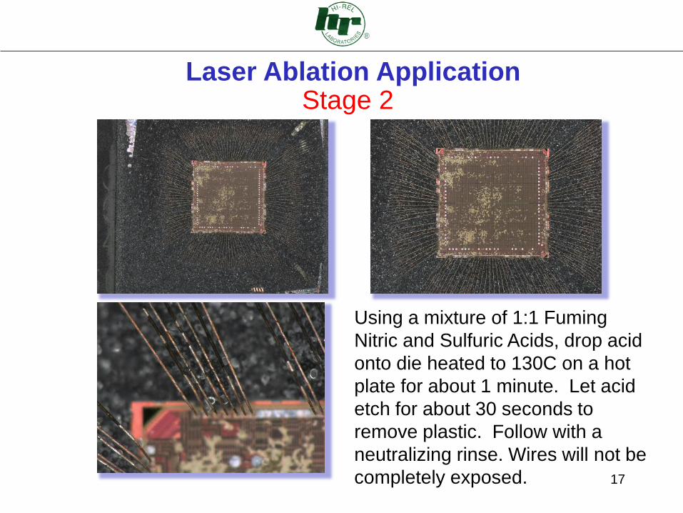
Laser Ablation ApplicationStage 2
Using a mixture of 1:1 Fuming Nitric and Sulfuric Acids, drop acid onto die heated to 130C on a hot plate for about 1 minute. Let acid etch for about 30 seconds to remove plastic. Follow with a neutralizing rinse. Wires will not be completely exposed.

18
Laser Ablation ApplicationStage 3
Ablate the area of the lead frame not previously exposed by acid etch to expose the lead frame bonds.

19
Laser Ablation Application- Lessons Learned
• Larger Copper Wire diameters fair better to acid and laser exposure.
• For the smallest wire diameters (~ 0.8 mil), you get one chance/exposure to acid etch the encapsulant away due to passivation layer removal at each exposure reducing the wire diameter.
• If you get too close to the Die Surface with laser ablation, you will damage the die and melt metallization. Remember glass bead fillers act as a conduit for laser.
• Too much power or too long a dwell time of the laser can overheat and damage/ablate copper bond wires

20
Laser Ablation Application- Lessons Learned
• This technique works great for Gold bond wires!
• Laser Ablation has also turned out to be an excellent way to get into stubborn magnetics and other difficult to depot components.
• Each part decapsulated is different. Settings for one part may or may not be the same for others from the same lot….some variations noted.

21
Mil-Std-1580 Rev. C
• The information gathered from these experiences was input into Requirement 16.5, the Plastic Encapsulated Microcircuit and Semiconductor DPA Procedure of Mil-Std-1580 Rev. C, hopefully out by year end, in an effort to share these techniques with industry.
• Mil-Std-1580C Requirement 16.5 now also addresses copper and silver wires.

Acknowledgements• I wanted to thank Damon Weaser in the lab at Hi-Rel
for all his efforts in preparation of the decapsulated devices discussed.
• I wanted to thank Mike Sampson and Ken LaBel for the opportunity to speak to you today.
22
In Closing“ The problem with doing something right thefirst time is that nobody appreciates howdifficult it was”….. Walt West