f2932 datasheet rev 1 5 4 16 final ec 05.12
TRANSCRIPT
F2932 Datasheet
High Reliability SP2T RF Switch 50 MHz to 8000 MHz
F2932, Rev 1 05/12/2016 1
GENERAL DESCRIPTION
The F2932 is a high reliability, low insertion loss, 50 Ω SP2T absorptive RF switch designed for a multitude of
wireless and other RF applications. This device covers a broad frequency range from 50 MHz to 8000 MHz.
In addition to providing low insertion loss, the F2932
also delivers high linearity and high isolation
performance while providing a 50 Ω termination to the
unused RF input port.
The F2932 uses a single positive supply voltage of 2.7 V to 5.5 V supporting three states using either
3.3 V or 1.8 V control logic.
COMPETITIVE ADVANTAGE
The F2932 provides the following advantages
Insertion Loss = 0.79 dB* RFX to RFC Isolation = 67 dB*
IIP3 = +64 dBm* Active Port Operating Power Handling = 34 dBm
Term Port Operating Power Handling = 27 dBm
Extended Temperature Range = -40°C to 105°C
* 2 GHZ
APPLICATIONS
• Base Station 2G, 3G, 4G
• Portable Wireless
• Repeaters and E911 systems
• Digital Pre-Distortion
• Point to Point Infrastructure
• Public Safety Infrastructure
• WIMAX Receivers and Transmitters
• Military Systems, JTRS radios
• RFID handheld and portable readers
• Test / ATE Equipment
FEATURES
• High Isolation:
o 70 dB @ 1 GHzo 67 dB @ 2 GHz
o 65 dB @ 3 GHzo 66 dB @ 4 GHz
• High Linearity:
o IIP2 of 111 dBm
o IIP3 of 64 dBm @ 2 GHz• Wide Single Positive Supply Voltage Range
• 3.3 V and 1.8 V compatible control logic
• Operating temperature -40 °C to +105 °C
• 4 mm x 4 mm 16 pin QFN package
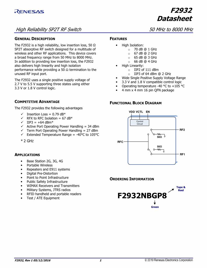
FUNCTIONAL BLOCK DIAGRAM
Control
Circuit
VDD ENVCTL
RFC
RF1
RF2
50Ω
50Ω
ORDERING INFORMATION
F2932NBGP8
Green
Tape & Reel

F2932
High Reliability SP2T RF Switch 2 F2932, Rev 1 05/12/2016
ABSOLUTE MAXIMUM RATINGS
Parameter / Condition Symbol Min Max Unit
VDD to GND VDD -0.3 +6.0 V
VCTL, EN to GND Vlogic -0.3Lower of
3.6, VDD+0.3 V
RF1, RF2, RFC to GND VRF -0.3 +0.3 V
RF Input Power 1
RF1 or RF2 as an input
(Connected to RFC) PRF12 36
dBm
RFC as an input (Connected to RF1 or RF2)
PRFC 36
RFC as an input
(All off state) PRFC_OFF 30
RF1 or RF2 as input
(Terminated states) PRF12_TERM 30
RF1 and RF2 as inputs (All Off State)
PRF12_OFF 30 2
Maximum Junction Temperature TJmax +140 °C
Storage Temperature Range TST -65 +150 °C
Lead Temperature (soldering, 10s) TLEAD +260 °C
ESD Voltage– HBM (Per JESD22-A114) VESDHBM Class 2 (2500V)
ESD Voltage – CDM (Per JESD22-C101) VESDCDM Class C3 (1000V)
Note 1: VDD = 2.7 V to 5.5 V, 50 MHz ≤ FRF ≤ 8000 MHz, Tc= 105 ºC, ZS = ZL = 50 ohms.
Note 2: Each port.
Stresses above those listed above may cause permanent damage to the device. Functional operation of the device at these or any other conditions above those indicated in the operational section of this specification is not implied. Exposure to absolute maximum rating conditions for extended periods may affect device reliability.
PACKAGE THERMAL AND MOISTURE CHARACTERISTICS
θJA (Junction – Ambient) 60 °C/W
θJC (Junction – Case) The Case is defined as the exposed paddle 3.9 °C/W
Moisture Sensitivity Rating (Per J-STD-020) MSL 1
F2932
F2932, Rev 1 05/12/2016 3 High Reliability SP2T RF Switch
F2932 RECOMMENDED OPERATING CONDITIONS
Parameter Symbol Condition Min Typ Max Units
Supply Voltage VDD 2.7 5.5 V
Operating Temp Range TCASE Exposed Paddle Temperature -40 +105 OC
RF Frequency Range FRF 50 8000 MHz
RF Continuous Input CW Power
(Non-Switched) 1
PRF
RFC connected to RF1
or RF22
TC =85 ºC 34
dBm
TC =105 ºC 34
RF1/ RF2 Input, Terminated State3, 4
TC =85 ºC 27
TC =105 ºC 27
RFC Input,
All off State
TC =85 ºC 27
TC =105 ºC 27
RF Continuous
Input Power
(RF Hot Switching CW) 1
PRFSW
RFC Input, switching between RF1 and RF2.
TC =85 ºC 30
dBm
TC =105 ºC 30
RFC Input, switching
into or out of All off State.
TC =85 ºC 27
TC =105 ºC 27
RF1 or RF2 as input,
switched between RFC and Term.
TC =85 ºC 27
TC =105 ºC 27
RF1 and RF2 as inputs,
switching into or out of All off State4.
TC =85 ºC 27
TC =105 ºC 27
RF1/2 Port Impedance ZRFx 50 Ω
RFC Port Impedance ZRFC 50
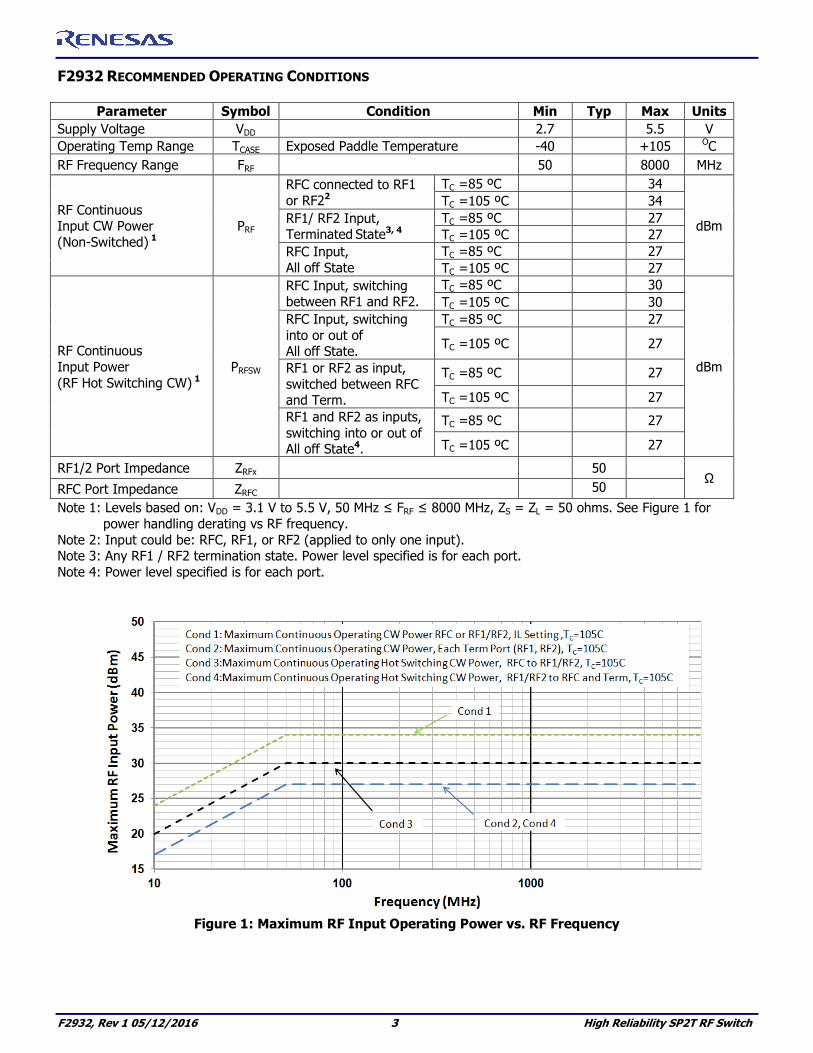
Note 1: Levels based on: VDD = 3.1 V to 5.5 V, 50 MHz ≤ FRF ≤ 8000 MHz, ZS = ZL = 50 ohms. See Figure 1 for
power handling derating vs RF frequency.
Note 2: Input could be: RFC, RF1, or RF2 (applied to only one input). Note 3: Any RF1 / RF2 termination state. Power level specified is for each port.
Note 4: Power level specified is for each port.
Figure 1: Maximum RF Input Operating Power vs. RF Frequency

F2932
High Reliability SP2T RF Switch 4 F2932, Rev 1 05/12/2016
F2932 SPECIFICATION Typical Application Circuit, VDD = 5.0 V, TC = +25 °C, FRF = 2000 MHz, Driven Port = RF1 or RF2, input power = 10 dBm, ZS = ZL = 50 ohms, PCB board trace and connector losses are de-embedded unless otherwise noted.
Parameter Symbol Condition Min Typ Max Units
Logic Input High Threshold VIH 1.1 Lower of (3.6, VDD)
V
Logic Input Low Threshold VIL -0.3 0.6 V
Logic Current IIH, IIL For each control pin -1 +1 µA
DC Current IDD VDD =3.3 V 200 260 1
µA VDD =5.0 V 260 325
Insertion Loss RFC to RF1 / RF2
IL
50 MHz 0.68
dB
1 GHz 0.73
2 GHz 0.79 1.1 3 GHz 0.82
4 GHz 0.93
6 GHz 1.06
8 GHz 1.6
Isolation RFC to RF1 / RF2
ISOC
50 MHz 772 79
dB
1 GHz 68 70
2 GHz 63 67
3 GHz 62 65
4 GHz 60 66
6 GHz 53 63
8 GHz 45
Isolation
RF1 to RF2 ISOX
50 MHz 86
dB
1 GHz 64
2 GHz 58
3 GHz 54
4 GHz 51
6 GHz 45
8 GHz 37
Return Loss
RFC, RF1, RF2 RFRL
50 MHz 25
dB
1 GHz 25
2 GHz 23
3 GHz 24
4 GHz 20
6 GHz 18
8 GHz 14
Return Loss RF1, RF2 Terminated
RFRLTERM
50 MHz 40 dB 1 GHz 31 2 GHz 35 3 GHz 23 4 GHz 17 6 GHz 19 8 GHz 22
Note 1: Items in min/max columns in bold italics are Guaranteed by Test. Note 2: Items in min/max columns that are not bold/italics are Guaranteed by Design Characterization.
F2932
F2932, Rev 1 05/12/2016 5 High Reliability SP2T RF Switch
F2932 SPECIFICATION (CONT.) Typical Application Circuit, VDD = 5.0 V, TC = +25 °C, FRF = 2000 MHz, Driven Port = RF1 or RF2, input power = 10 dBm, ZS = ZL = 50 ohms, PCB board trace and connector losses are de-embedded unless otherwise noted.
Parameter Symbol Condition Min Typ Max Units
Input 1dB Compression3 ICP1dB
50 MHz 33.2
dBm
1 GHz 35.5 2 GHz 36.5 3 GHz 36.1 4 GHz 35.3
Input 0.1dB Compression3 ICP0.1dB
VDD = 5.0 V
50 MHz 30.4
dBm
2 GHz 32.3
3 GHz 32.6
4 GHz 32.2
VDD = 3.1 V
50 MHz 30.1
2 GHz 32.1
3 GHz 32.6
4 GHz 32.1
Input IP2 IIP2
FRF1 = 2000 MHz, FRF2 = 1990 MHz RFIN = RF1 or RF2
PIN = +20 dBm / tone FIP2 =FRF1 + FRF2
111 dBm
Input IP3 IIP3 RF Input = RF1 or RF2 PIN = +15 dBm/tone
∆ F = 1 MHz
50 MHz 58
dBm
1 GHz 64
2 GHz 64
2.5 GHz 63.4
4 GHz 63.6
Non-RF Driven Spurious4 SpurMAX At any RF port when externally terminated into 50 Ω
-114 dBm
Switching Time5 TSW
50% control to 90% RF 210
ns 50% control to 10% RF 115 50% control to RF settled to within
+/- 0.1 dB of I.L. value 225
Maximum Switching Rate6 SWRATE 25 kHz
Maximum Video Feed-through on RF Ports
VIDFT 5 MHz to 1000 MHz Measured with 20 ns risetime,
0 to 3.3 V control pulse 12 mVpp
Note 1: Items in min/max columns in bold italics are Guaranteed by Test. Note 2: Items in min/max columns that are not bold/italics are Guaranteed by Design Characterization.
Note 3: The input 1 dB compression point is a linearity figure of merit. Refer to the Recommended Operating
Conditions section for the specified maximum operating power levels. Note 4: Spurious due to on-chip negative voltage generator. Typical generator fundamental frequency is 5.2 MHz.
Note 5: FRF = 1 GHz. Note 6: Minimum time required between switching of states = 1/ (Maximum Switching Rate).
F2932
High Reliability SP2T RF Switch 6 F2932, Rev 1 05/12/2016
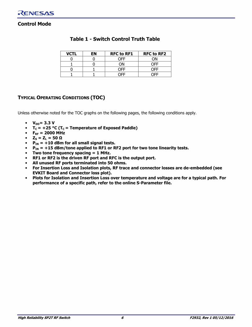
Control Mode
Table 1 - Switch Control Truth Table
VCTL EN RFC to RF1 RFC to RF2
0 0 OFF ON
1 0 ON OFF
0 1 OFF OFF
1 1 OFF OFF
TYPICAL OPERATING CONDITIONS (TOC)
Unless otherwise noted for the TOC graphs on the following pages, the following conditions apply.
• VDD= 3.3 V
• TC = +25 °C (TC = Temperature of Exposed Paddle)
• FRF = 2000 MHz
• ZS = ZL = 50 Ω
• PIN = +10 dBm for all small signal tests.
• PIN = +15 dBm/tone applied to RF1 or RF2 port for two tone linearity tests.
• Two tone frequency spacing = 1 MHz.
• RF1 or RF2 is the driven RF port and RFC is the output port.
• All unused RF ports terminated into 50 ohms.
• For Insertion Loss and Isolation plots, RF trace and connector losses are de-embedded (see
EVKIT Board and Connector loss plot).• Plots for Isolation and Insertion Loss over temperature and voltage are for a typical path. For
performance of a specific path, refer to the online S-Parameter file.

F2932
F2932, Rev 1 05/12/2016 7 High Reliability SP2T RF Switch
TYPICAL OPERATING CONDITIONS (- 1 -)
RF1 to RFC Insertion Loss
RF1 Port Match [On State]
RF1 Port Match [Terminated State]
RF2 to RFC Insertion Loss
RF2 Port Match [On State]
RF2 Port Match [Terminated State]
-2
-1.5
-1
-0.5
0
0 1 2 3 4 5 6 7 8
Ins
ert
ion
Lo
ss
(dB
)
Frequency (GHz)
2.7V, -40C 3.3V, -40C 5.0V, -40C 5.5V, -40C
2.7V, 25C 3.3V, 25C 5.0V, 25C 5.5V, 25C
2.7V, 105C 3.3V, 105C 5.0V, 105C 5.5V, 105C
-40
-35
-30
-25
-20
-15
-10
-5
0
0 1 2 3 4 5 6 7 8
Ma
tch
(dB
)
Frequency (GHz)
2.7V, -40C 3.3V, -40C 5.0V, -40C 5.5V, -40C
2.7V, 25C 3.3V, 25C 5.0V, 25C 5.5V, 25C
2.7V, 105C 3.3V, 105C 5.0V, 105C 5.5V, 105C
-40
-35
-30
-25
-20
-15
-10
-5
0
0 1 2 3 4 5 6 7 8
Ma
tch
(dB
)
Frequency (GHz)
2.7V, -40C 3.3V, -40C 5.0V, -40C 5.5V, -40C
2.7V, 25C 3.3V, 25C 5.0V, 25C 5.5V, 25C
2.7V, 105C 3.3V, 105C 5.0V, 105C 5.5V, 105C

F2932
High Reliability SP2T RF Switch 8 F2932, Rev 1 05/12/2016
TYPICAL OPERATING CONDITIONS (- 2 -)
RFC Port Match [RF1 On State]
RF1 to RFC Isolation [RF2 On State]
RF1 to RF2 Isolation [RF1 On State]
RFC Port Match [RF2 On State]
RF2 to RFC Isolation [RF1 On State]
RF2 to RF1 Isolation [RF2 On State]
-40
-35
-30
-25
-20
-15
-10
-5
0
0 1 2 3 4 5 6 7 8
Ma
tch
(dB
)
Frequency (GHz)
2.7V, -40C 3.3V, -40C 5.0V, -40C 5.5V, -40C
2.7V, 25C 3.3V, 25C 5.0V, 25C 5.5V, 25C
2.7V, 105C 3.3V, 105C 5.0V, 105C 5.5V, 105C
-100
-90
-80
-70
-60
-50
-40
-30
-20
-10
0
0 1 2 3 4 5 6 7 8
Iso
lati
on
(dB
)
Frequency (GHz)
2.7V, -40C 3.3V, -40C 5.0V, -40C 5.5V, -40C
2.7V, 25C 3.3V, 25C 5.0V, 25C 5.5V, 25C
2.7V, 105C 3.3V, 105C 5.0V, 105C 5.5V, 105C
-100
-90
-80
-70
-60
-50
-40
-30
-20
-10
0
0 1 2 3 4 5 6 7 8
Iso
lati
on
(dB
)
Frequency (GHz)
2.7V, -40C 3.3V, -40C 5.0V, -40C 5.5V, -40C
2.7V, 25C 3.3V, 25C 5.0V, 25C 5.5V, 25C
2.7V, 105C 3.3V, 105C 5.0V, 105C 5.5V, 105C
-40
-35
-30
-25
-20
-15
-10
-5
0
0 1 2 3 4 5 6 7 8
Ma
tch
(dB
)
Frequency (GHz)
2.7V, -40C 3.3V, -40C 5.0V, -40C 5.5V, -40C
2.7V, 25C 3.3V, 25C 5.0V, 25C 5.5V, 25C
2.7V, 105C 3.3V, 105C 5.0V, 105C 5.5V, 105C
-100
-90
-80
-70
-60
-50
-40
-30
-20
-10
0
0 1 2 3 4 5 6 7 8
Iso
lati
on
(dB
)
Frequency (GHz)
2.7V, -40C 3.3V, -40C 5.0V, -40C 5.5V, -40C
2.7V, 25C 3.3V, 25C 5.0V, 25C 5.5V, 25C
2.7V, 105C 3.3V, 105C 5.0V, 105C 5.5V, 105C
-100
-90
-80
-70
-60
-50
-40
-30
-20
-10
0
0 1 2 3 4 5 6 7 8
Iso
lati
on
(dB
)
Frequency (GHz)
2.7V, -40C 3.3V, -40C 5.0V, -40C 5.5V, -40C
2.7V, 25C 3.3V, 25C 5.0V, 25C 5.5V, 25C
2.7V, 105C 3.3V, 105C 5.0V, 105C 5.5V, 105C
F2932
F2932, Rev 1 05/12/2016 9 High Reliability SP2T RF Switch
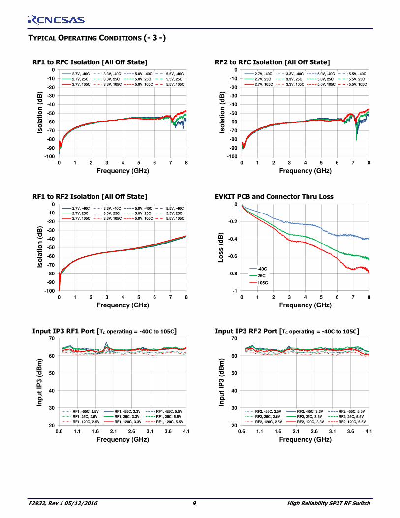
TYPICAL OPERATING CONDITIONS (- 3 -)
RF1 to RFC Isolation [All Off State]
RF1 to RF2 Isolation [All Off State]
Input IP3 RF1 Port [TC operating = -40C to 105C]
RF2 to RFC Isolation [All Off State]
EVKIT PCB and Connector Thru Loss
Input IP3 RF2 Port [TC operating = -40C to 105C]
-100
-90
-80
-70
-60
-50
-40
-30
-20
-10
0
0 1 2 3 4 5 6 7 8
Iso
lati
on
(dB
)
Frequency (GHz)
2.7V, -40C 3.3V, -40C 5.0V, -40C 5.5V, -40C
2.7V, 25C 3.3V, 25C 5.0V, 25C 5.5V, 25C
2.7V, 105C 3.3V, 105C 5.0V, 105C 5.5V, 105C
-100
-90
-80
-70
-60
-50
-40
-30
-20
-10
0
0 1 2 3 4 5 6 7 8
Iso
lati
on
(dB
)
Frequency (GHz)
2.7V, -40C 3.3V, -40C 5.0V, -40C 5.5V, -40C
2.7V, 25C 3.3V, 25C 5.0V, 25C 5.5V, 25C
2.7V, 105C 3.3V, 105C 5.0V, 105C 5.5V, 105C
20
30
40
50
60
70
0.6 1.1 1.6 2.1 2.6 3.1 3.6 4.1
Inp
ut
IP3
(dB
m)
Frequency (GHz)
RF1, -55C, 2.5V RF1, -55C, 3.3V RF1, -55C, 5.5V
RF1, 25C, 2.5V RF1, 25C, 3.3V RF1, 25C, 5.5V
RF1, 120C, 2.5V RF1, 120C, 3.3V RF1, 120C, 5.5V
-100
-90
-80
-70
-60
-50
-40
-30
-20
-10
0
0 1 2 3 4 5 6 7 8
Iso
lati
on
(dB
)
Frequency (GHz)
2.7V, -40C 3.3V, -40C 5.0V, -40C 5.5V, -40C
2.7V, 25C 3.3V, 25C 5.0V, 25C 5.5V, 25C
2.7V, 105C 3.3V, 105C 5.0V, 105C 5.5V, 105C
-1
-0.8
-0.6
-0.4
-0.2
0
0 1 2 3 4 5 6 7 8
Lo
ss
(dB
)
Frequency (GHz)
-40C
25C
105C
20
30
40
50
60
70
0.6 1.1 1.6 2.1 2.6 3.1 3.6 4.1
Inp
ut
IP3
(d
Bm
)
Frequency (GHz)
RF2, -55C, 2.5V RF2, -55C, 3.3V RF2, -55C, 5.5V
RF2, 25C, 2.5V RF2, 25C, 3.3V RF2, 25C, 5.5V
RF2, 120C, 2.5V RF2, 120C, 3.3V RF2, 120C, 5.5V

F2932
High Reliability SP2T RF Switch 10 F2932, Rev 1 05/12/2016
TYPICAL OPERATING CONDITIONS (- 4 -)
Input P1dB [1GHz] [TC operating = -40C to 105C]
-1
-0.9
-0.8
-0.7
-0.6
-0.5
-0.4
-0.3
-0.2
-0.1
0
25 26 27 28 29 30 31 32 33 34 35 36 37 38
Co
mp
res
sio
n (
dB
)
Input Power (dBm)
-55C
25C
125C

F2932
F2932, Rev 1 05/12/2016 11 High Reliability SP2T RF Switch
PACKAGE DRAWING
(4 mm x 4 mm 16-pin QFN), NBG16
Note: The F2932 uses EPAD Option P1 and Lead Option Z1

F2932
High Reliability SP2T RF Switch 12 F2932, Rev 1 05/12/2016
LAND PATTERN DIMENSION

F2932
F2932, Rev 1 05/12/2016 13 High Reliability SP2T RF Switch
PIN DIAGRAM
VDD 1
4
3
2
RFC
GND
GN
D
EN
GN
D
GND
VCTL
E.P.
12
9
10
11
7 865
14
13
15
16
GN
D
RF1
GND
RF2
GN
D
N/C
GN
D
GN
D
50Ω
50Ω
PIN DESCRIPTION
PIN NAME FUNCTION
1 VDD Power Supply. Bypass to GND with capacitors shown in the
Typical Application Circuit as close as possible to pin.
2 VCTL Controls the selected path when EN is low. Is disabled when EN is logic high. See Table 1.
3 RFC RF Common Port. Matched to 50 Ω when one of the 2 RF ports
is selected. If this pin is not 0 V DC, then an external coupling
capacitor must be used.
4, 6, 7, 8, 10,
11, 13, 14, 15,
16
GND Ground. Also, internally connected to the ground paddle. Ground this pin as close to the device as possible.
5 EN
EN as a logic low allows VCTL to control the selected switch
path. With EN set to logic high puts the part in all paths off state and disables the control of VCTL. See Table 1.
9 RF1 RF1 Port. Matched to 50 Ω. If this pin is not 0 V DC, then an
external coupling capacitor must be used.
12 RF2 RF2 Port. Matched to 50 Ω. If this pin is not 0 V DC, then an
external coupling capacitor must be used.
17 — EP
Exposed Pad. Internally connected to GND. Solder this exposed pad to a PCB pad that uses multiple ground vias to provide heat
transfer out of the device and into the PCB ground planes. These
multiple ground vias are also required to achieve the specified RF performance.

F2932
High Reliability SP2T RF Switch 14 F2932, Rev 1 05/12/2016
APPLICATIONS INFORMATION
Default Start-up
There are no internal pull-up or pull-down resistors on the VCTL or EN pins.
Logic Control
Control pins VCTL and EN are used to set the state of the SP2T switch (see Table 1).
Power Supplies
A common VCC power supply should be used for all pins requiring DC power. All supply pins should be bypassed with external capacitors to minimize noise and fast transients. Supply noise can degrade noise figure
and fast transients can trigger ESD clamps and cause them to fail. Supply voltage change or transients should have a slew rate smaller than 1 V / 20 µs. In addition, all control pins should remain at 0 V (+/- 0.3 V) while
the supply voltage ramps or while it returns to zero.
Control Pin Interface
If control signal integrity is a concern and clean signals cannot be guaranteed due to overshoot, undershoot, ringing, etc., the following circuit at the input of each control pin is recommended. This applies to control
pin 2 (VCTL) and pin 5 (EN) as shown below.
1
4
3
2
12
9
10
11
7 865
14
13
15
16
50Ω
50Ω
EN
5k ohm
2pF
VCTL
5k ohm
2pF
F2932
F2932, Rev 1 05/12/2016 15 High Reliability SP2T RF Switch
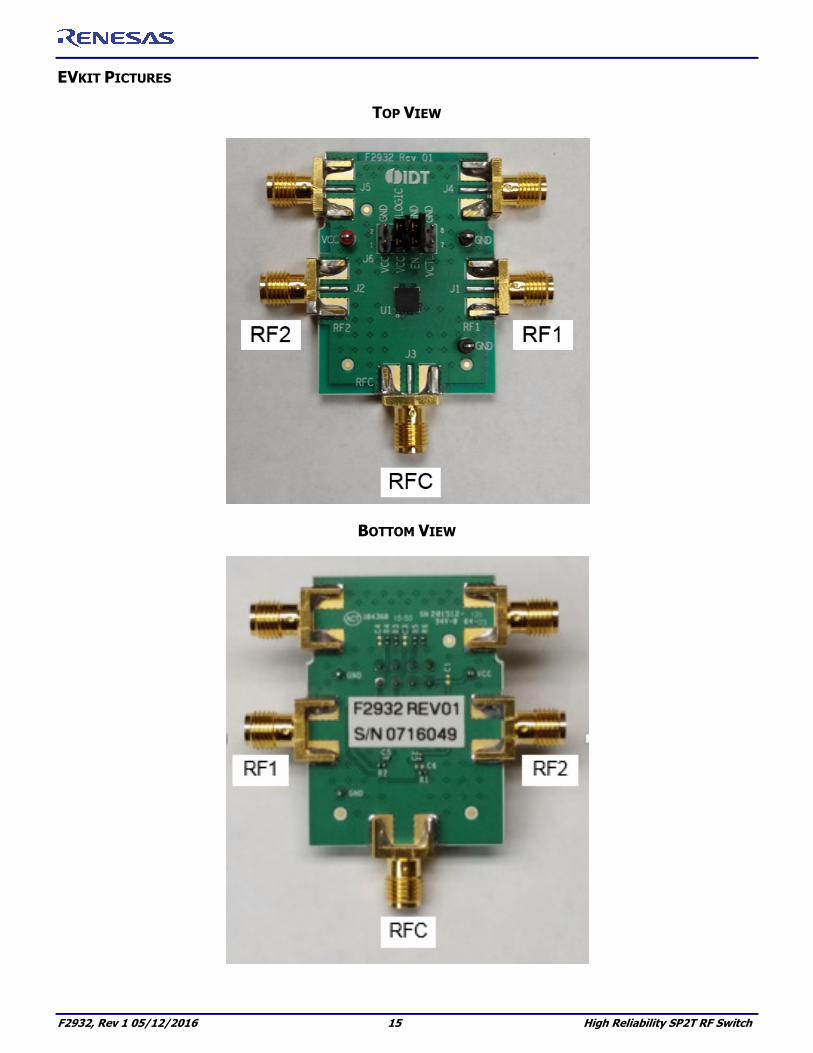
EVKIT PICTURES
TOP VIEW
BOTTOM VIEW
F2932
High Reliability SP2T RF Switch 16 F2932, Rev 1 05/12/2016
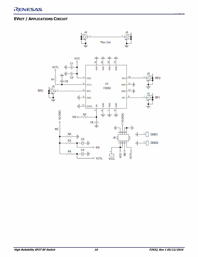
EVKIT / APPLICATIONS CIRCUIT
F2932
F2932, Rev 1 05/12/2016 17 High Reliability SP2T RF Switch
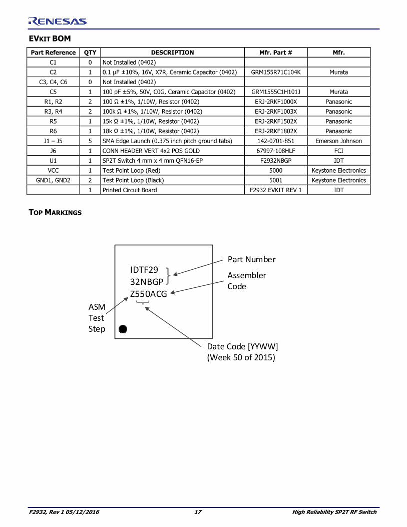
EVKIT BOM
Part Reference QTY DESCRIPTION Mfr. Part # Mfr.
C1 0 Not Installed (0402)
C2 1 0.1 µF ±10%, 16V, X7R, Ceramic Capacitor (0402) GRM155R71C104K Murata
C3, C4, C6 0 Not Installed (0402)
C5 1 100 pF ±5%, 50V, C0G, Ceramic Capacitor (0402) GRM1555C1H101J Murata
R1, R2 2 100 Ω ±1%, 1/10W, Resistor (0402) ERJ-2RKF1000X Panasonic
R3, R4 2 100k Ω ±1%, 1/10W, Resistor (0402) ERJ-2RKF1003X Panasonic
R5 1 15k Ω ±1%, 1/10W, Resistor (0402) ERJ-2RKF1502X Panasonic
R6 1 18k Ω ±1%, 1/10W, Resistor (0402) ERJ-2RKF1802X Panasonic
J1 – J5 5 SMA Edge Launch (0.375 inch pitch ground tabs) 142-0701-851 Emerson Johnson
J6 1 CONN HEADER VERT 4x2 POS GOLD 67997-108HLF FCI
U1 1 SP2T Switch 4 mm x 4 mm QFN16-EP F2932NBGP IDT
VCC 1 Test Point Loop (Red) 5000 Keystone Electronics
GND1, GND2 2 Test Point Loop (Black) 5001 Keystone Electronics
1 Printed Circuit Board F2932 EVKIT REV 1 IDT
TOP MARKINGS
IDTF29
32NBGP
Z550ACG
Part Number
Date Code [YYWW]
(Week 50 of 2015)
ASM
Test
Step
Assembler
Code

F2932
High Reliability SP2T RF Switch 18 F2932, Rev 1 05/12/2016
EVKIT OPERATION
External Supply Setup
Set up a VCC power supply in the voltage range of 2.7 V to 5.5 V and disable the power supply output.
Logic Control Setup
Using the EVKIT to manually set the control logic:
On connector J6 connect a 2-pin shunt from pin 3 (VCC) to pin 4 (VLOGIC). This connection provides the
VCC voltage supply to the Eval Board logic control pull up network. Resistors R5 and R6 form a voltage divider to set the Vhigh level over the 2.7 V to 5.5 V VCC range for manual logic control.
Connector J6 has 2 logic input pins: EN (pin 5) and VCTL (pin 7). See Table 1 for Logic Truth Table. With
the pullup network enabled (as noted above) these pins can be left open to provide a logic high through pull up resistors R3 and R4. To set a logic low for EN and VCTL connect 2-pin shunts on J6 from pin 5
(EN) to pin 6 (GND) and from pin 7 (VCTL) to pin 8 (GND).
Note that when using the on board R5 / R6 voltage divider the current draw from the VCC supply will be
higher by approximately VCC / 33k Ω.
Using external control logic:
Pins 3, 4, 6, and 8 of J6 should have no external connection. External logic controls are applied to J6 pin 5
(EN) and pin 7 (VCTL). See Table 1 for Logic Truth Table.
Turn on Procedure
Setup the supplies and Eval Board as noted in the External Supply Setup and Logic Control Setup
sections above.
Connect the preset disabled VCC power supply to the red VCC loop and ground to GND1 or GND2.
Enable the VCC supply.
Set the desired logic setting using J6 pin 5 (EN) and pin 7 (VCTL) to achieve the desired Table 1 setting.
Note that external control logic should not be applied without VCC being present.
Turn off Procedure
If using external control logic for EN and VCTL then set them to a logic low.
Disable the VCC supply.
F2932
F2932, Rev 1 05/12/2016 19 High Reliability SP2T RF Switch
Revision History Sheet
Rev Date Page Description of Change O 2016-Feb-26 Initial release
1 2016-May-03 1-5, 13, 15 Updates

F2932
High Reliability SP2T RF Switch 20 F2932, Rev 1 05/12/2016
Corporate Headquarters 6024 Silver Creek Valley Road San Jose, CA 95138 USA
Sales 1-800-345-7015 or 408-284-8200 Fax: 408-284-2775 www.idt.com
Tech Support http://www.idt.com/support/technical-support
DISCLAIMER Integrated Device Technology, Inc. (IDT) reserves the right to modify the products and/or specifications described herein at any time, without notice, at IDT’s sole discretion.
Performance specifications and operating parameters of the described products are determined in an independent state and are not guaranteed to perform the same way when installed in customer products. The information contained herein is provided without representation or warranty of any kind, whether express or implied, including, but not limited to, the suitability of IDT’s products for any particular purpose, an implied warranty of merchantability, or non-infringement of the intellectual property rights of others. This document is presented only as a guide and does not convey any
license under intellectual property rights of IDT or any third parties.
IDT’s products are not intended for use in applications involving extreme environmental conditions or in life support systems or similar devices where the failure or malfunction of an IDT product can
be reasonably expected to significantly affect the health or safety of users. Anyone using an IDT product in such a manner does so at their own risk, absent an express, written agreement by IDT.
Integrated Device Technology, IDT and the IDT logo are trademarks or registered trademarks of IDT and its subsidiaries in the United States and other countries. Other trademarks used herein are the property of IDT or their respective third party owners.
Copyright ©2015. Integrated Device Technology, Inc. All rights reserved.

Corporate HeadquartersTOYOSU FORESIA, 3-2-24 Toyosu,Koto-ku, Tokyo 135-0061, Japanwww.renesas.com
Contact InformationFor further information on a product, technology, the most up-to-date version of a document, or your nearest sales office, please visit:www.renesas.com/contact/
TrademarksRenesas and the Renesas logo are trademarks of Renesas Electronics Corporation. All trademarks and registered trademarks are the property of their respective owners.
IMPORTANT NOTICE AND DISCLAIMER
RENESAS ELECTRONICS CORPORATION AND ITS SUBSIDIARIES (“RENESAS”) PROVIDES TECHNICAL SPECIFICATIONS AND RELIABILITY DATA (INCLUDING DATASHEETS), DESIGN RESOURCES (INCLUDING REFERENCE DESIGNS), APPLICATION OR OTHER DESIGN ADVICE, WEB TOOLS, SAFETY INFORMATION, AND OTHER RESOURCES “AS IS” AND WITH ALL FAULTS, AND DISCLAIMS ALL WARRANTIES, EXPRESS OR IMPLIED, INCLUDING, WITHOUT LIMITATION, ANY IMPLIED WARRANTIES OF MERCHANTABILITY, FITNESS FOR A PARTICULAR PURPOSE, OR NON-INFRINGEMENT OF THIRD PARTY INTELLECTUAL PROPERTY RIGHTS.
These resources are intended for developers skilled in the art designing with Renesas products. You are solely responsible for (1) selecting the appropriate products for your application, (2) designing, validating, and testing your application, and (3) ensuring your application meets applicable standards, and any other safety, security, or other requirements. These resources are subject to change without notice. Renesas grants you permission to use these resources only for development of an application that uses Renesas products. Other reproduction or use of these resources is strictly prohibited. No license is granted to any other Renesas intellectual property or to any third party intellectual property. Renesas disclaims responsibility for, and you will fully indemnify Renesas and its representatives against, any claims, damages, costs, losses, or liabilities arising out of your use of these resources. Renesas' products are provided only subject to Renesas' Terms and Conditions of Sale or other applicable terms agreed to in writing. No use of any Renesas resources expands or otherwise alters any applicable warranties or warranty disclaimers for these products.
(Rev.1.0 Mar 2020)
© 2020 Renesas Electronics Corporation. All rights reserved.