igd opregion/software sci/_dsm for skylake processors
TRANSCRIPT

IGD OpRegion/Software SCI/ _DSM for Skylake Processors BIOS Specification September 2016 Revision 0.5


1
You may not use or facilitate the use of this document in connection with any infringement or other legal analysis concerning
Intel products described herein. You agree to grant Intel a non-exclusive, royalty-free license to any patent claim thereafter
drafted which includes subject matter disclosed herein.
No license (express or implied, by estoppel or otherwise) to any intellectual property rights is granted by this document.
Intel technologies’ features and benefits depend on system configuration and may require enabled hardware, software or service
activation. Performance varies depending on system configuration. No computer system can be absolutely secure. Check with
your system manufacturer or retailer or learn more at intel.com.
Intel technologies may require enabled hardware, specific software, or services activation. Check with your system manufacturer
or retailer.
The products described may contain design defects or errors known as errata which may cause the product to deviate from
published specifications. Current characterized errata are available on request.
Intel disclaims all express and implied warranties, including without limitation, the implied warranties of merchantability, fitness
for a particular purpose, and non-infringement, as well as any warranty arising from course of performance, course of dealing, or
usage in trade.
All information provided here is subject to change without notice. Contact your Intel representative to obtain the latest Intel
product specifications and roadmaps.
Copies of documents which have an order number and are referenced in this document may be obtained by calling 1-800-548-
4725 or visit www.intel.com/design/literature.htm.
Intel, Intel Inside, the Intel logo, Intel Inside logo, Intel Core, Intel Atom, Pentium, Celeron, 3D XPoint, Experience What’s
Inside, Experience What’s Inside logo, Intel Unite, Intel vPro, Intel RealSense, Intel SpeedStep, Iris, Optane, Thunderbolt, the
Thunderbolt logo and True Key are trademarks of Intel Corporation in the United States and other countries.
*Other names and brands may be claimed as the property of others.
Copyright © 2016, Intel Corporation.

2
Contents 1 Introduction .................................................................................................... 1
1.1 Terminology ......................................................................................... 2 1.2 Objective ............................................................................................. 3 1.3 Intended Audience ................................................................................ 4 1.4 Scope .................................................................................................. 4 1.5 Reasons for Replacing SMI and INT 10h .................................................... 4 1.6 Reference Documents ............................................................................ 5
2 Overview ........................................................................................................ 6 2.1 OpRegion Types and Definitions .............................................................. 7 2.2 GMCH PCI Config OpRegion .................................................................... 8 2.3 Memory OpRegion ................................................................................. 9
3 OpRegion Memory Layout ............................................................................... 11 3.1 OpRegion Header ................................................................................ 12
3.1.1 Signature (SIGN) ................................................................... 13 3.1.2 Size (SIZE) ........................................................................... 14 3.1.3 OpRegion Version (OVER) ........................................................ 14 3.1.4 System BIOS Version (SVER) ................................................... 15 3.1.5 Video BIOS Version (VVER) ...................................................... 16 3.1.6 Graphics Driver Version (GVER) ................................................ 17 3.1.7 Supported Mailboxes (MBOX) ................................................... 17 3.1.8 Driver Model (DMOD) .............................................................. 18 3.1.9 Platform Configuration (PCON) ................................................. 19 3.1.10 GOP Version (DVER) ............................................................... 21
3.2 Mailbox 1: Public ACPI Methods ............................................................. 21 3.2.1 Driver Ready (DRDY) .............................................................. 23 3.2.2 Notification Status (CSTS) ....................................................... 25 3.2.3 Current Event (CEVT) ............................................................. 27 3.2.4 Supported Display Devices ID List (DIDL) .................................. 28 3.2.5 Currently Attached Display Devices List (CPDL) ........................... 30 3.2.6 Currently Active Display Devices List (CADL) .............................. 32 3.2.7 Next Active Display Devices List (NADL) .................................... 33 3.2.8 ASL Sleep Time-out (ASLP) ...................................................... 35 3.2.9 Toggle Table Index (TIDX) ....................................................... 36 3.2.10 Current Hot Plug Enable Indicator (CHPD) .................................. 37 3.2.11 Current Lid State Indicator (CLID) ............................................ 38 3.2.12 Current Docking State Indicator (CDCK) .................................... 39 3.2.13 Sx State Resume (SXSW) ........................................................ 40 3.2.14 ASL Supported Events (EVTS) .................................................. 41

3
3.2.15 Current OS Notifications (CNOT) ............................................... 42 3.2.16 Driver Status (NRDY) .............................................................. 44
3.3 Mailbox 2: Software SCI Interface ......................................................... 45 3.3.1 Software SCI Entry/Exit Parameters (SCIC) ............................... 46 3.3.2 Additional Parameters (PARM) .................................................. 49 3.3.3 Driver Sleep Timeout (DSLP) ................................................... 49
3.4 Mailbox 3: BIOS to Driver Notification .................................................... 50 3.4.1 Driver Readiness (ARDY) ......................................................... 52 3.4.2 ASLE Interrupt Command (ASLC) ............................................. 53 3.4.3 Technology Enabled Indicator (TCHE) ........................................ 56 3.4.4 Current ALS Illuminance Reading (ALSI) .................................... 58 3.4.5 Backlight Brightness (BCLP) ..................................................... 58 3.4.6 Panel Fitting (PFIT) ................................................................. 59 3.4.7 Current Brightness Level (CBLV) ............................................... 60 3.4.8 Backlight Brightness Level Duty Cycle Mapping Table .................. 61 3.4.9 Current Panel Fitting Mode (CPFM) ............................................ 62 3.4.10 Enabled Panel Fitting Modes (EPFM) .......................................... 63 3.4.11 Panel LUT and Identifier (PLUT) ................................................ 64 3.4.12 PWM Frequency and Minimum Brightness (PFMB) ........................ 66 3.4.13 Color Correction Default Values (CCDV) ..................................... 66 3.4.14 Power Conservation Features (PCFT) ......................................... 67 3.4.15 Supported Rotation Angles (SROT) ........................................... 68 3.4.16 Intel Ultrabook™ Event Register (IUER) ..................................... 69 3.4.17 FDSS .................................................................................... 70 3.4.18 FDSP .................................................................................... 70 3.4.19 STAT .................................................................................... 70
3.5 Mailbox 4: Video BIOS Table (VBT) ........................................................ 71 3.5.1 Video BIOS Table (VBT) Usage ................................................. 71
3.6 Mailbox 5: BIOS to Driver Notification Extension ...................................... 73 3.6.1 Panel Header (PHED) .............................................................. 74 3.6.2 Panel EDID Block (BDDC) ........................................................ 74
4 Software SCI Mechanism ................................................................................ 76 4.1 Software SCI Parameters ..................................................................... 76
4.1.1 Entry: Function Codes ............................................................. 77 4.1.2 Exit: Call Status Results .......................................................... 77
4.2 Software SCI Function Descriptions ........................................................ 78 4.2.1 Get BIOS Data (GBDA)............................................................ 78 4.2.2 Supported Calls ..................................................................... 79 4.2.3 Requested System Callbacks .................................................... 80 4.2.4 Boot Display Preferences ......................................................... 83 4.2.5 Get Panel Details .................................................................... 86 4.2.6 Internal Graphics Settings ....................................................... 88

4
4.2.7 Spread Spectrum Clocks.......................................................... 90 4.2.8 Get AKSV .............................................................................. 91 4.2.9 System BIOS Callbacks ........................................................... 92 4.2.10 Supported Callbacks ............................................................... 93 4.2.11 BIOS Initialization Completion Notification ................................. 96 4.2.12 Pre-Hires Set Mode ................................................................. 96 4.2.13 Post-Hires Set Mode ............................................................... 97 4.2.14 Display Switch ....................................................................... 98 4.2.15 Adapter Power State Notification ............................................. 100 4.2.16 Display Power State Notification .............................................. 101 4.2.17 Set Boot Display Preference .................................................... 102 4.2.18 Set Panel Preference .............................................................. 104 4.2.19 Set Internal Graphics Preference ............................................. 106 4.2.20 Switch to Full-Screen ............................................................. 107 4.2.21 APM Complete ...................................................................... 107 4.2.22 Set Spread Spectrum Clocks ................................................... 108 4.2.23 Post VBE/PM Set Power STATE NOTIFICATION ........................... 109 4.2.24 Set PAVP Data ...................................................................... 110
5 BIOS Writers Guide ....................................................................................... 112 5.1 SCI Hardware Register Reference ......................................................... 112
5.1.1 GMCH SWSCI Register ........................................................... 112 5.1.2 GMCH ASLS Register ............................................................. 114 5.1.3 ICH TSTS1 – TCO1_STS Register ............................................. 114 5.1.4 ASLE – System Display Event Register ..................................... 115 5.1.5 LBB — Legacy Backlight Brightness .......................................... 116
5.2 ACPI Spec Reference .......................................................................... 117 5.2.1 NVS Memory Reference .......................................................... 118 5.2.2 Video Extensions Reference .................................................... 118 5.2.3 Device Attribute Reference ..................................................... 119
5.3 Initialization (POST) Code .................................................................... 120 5.3.1 Create NVS Memory OpRegion ................................................ 121 5.3.2 Initialize IGD Global NVS Area ................................................. 121 5.3.3 Initialize OpRegion ................................................................ 121 5.3.4 Retrieving Video BIOS Build Number ........................................ 122 5.3.5 Retrieving VBT ...................................................................... 122 5.3.6 Invalid VBT .......................................................................... 124 5.3.7 Initialize Hardware State ........................................................ 124
5.4 ASL Software SCI Handler ................................................................... 125 5.5 ASL Functions .................................................................................... 125 5.6 Remove MBI/SMI Functionality ............................................................. 125 5.7 Building ............................................................................................ 126
6 Device Specific Methods “_DSM” ..................................................................... 127

5
6.1 GMCH’s “_DSM” Definition ................................................................... 127 6.1.1 Get BIOS Data Functions Supported “Function #0” ..................... 128 6.1.2 Adapter Power State Notification “Function #1” ......................... 130 6.1.3 Display Power State Notification “Function #2” .......................... 130 6.1.4 System BIOS POST Completion Notification “Function #3” ........... 131 6.1.5 Pre-Hires Set Mode “Function #4” ............................................ 131 6.1.6 Post-Hires Set Mode “Function #5” .......................................... 132 6.1.7 Set Display Device Notification “Function #6” ............................ 132 6.1.8 Set Boot Device Preference “Function #7” ................................. 132 6.1.9 Set Panel Preference “Function #8” .......................................... 133 6.1.10 Full Screen DOS “Function #9” ................................................ 134 6.1.11 APM Complete “Function #10” ................................................. 135 6.1.12 Unplug Plug Audio “Function #11” ........................................... 135 6.1.13 Core Display Clock Change Notification “Function #12” ............... 135 6.1.14 Get Boot Display Preference “Function #13” .............................. 136 6.1.15 Get Panel Detail “Function #14” .............................................. 139 6.1.16 Get Internal Graphics “Function #15” ....................................... 139 6.1.17 Get AKSV “Function #16” ....................................................... 141

6
Figures
Figure 2-1. ASL Methods Diagram ...................................................................... 7 Figure 3-1. VBT Instances and Flow .................................................................. 73 Figure 5-1. Locating VBT and Determining Size ................................................. 123
Tables
Table 2-1. PCI OpRegion Registers ..................................................................... 8 Table 3-1. OpRegion Layout ............................................................................ 11 Table 3-2. OpRegion Header Layout .................................................................. 12 Table 3-3. Header SIGN Field .......................................................................... 13 Table 3-4. Header SIZE Field ........................................................................... 14 Table 3-5. Header OVER Field .......................................................................... 15 Table 3-6. Header SVER Field .......................................................................... 16 Table 3-7. Header VVER Field .......................................................................... 16 Table 3-8. Header GVER Field .......................................................................... 17 Table 3-9. Header MBOX Field ......................................................................... 17 Table 3-10. Header DMOD Field ....................................................................... 19 Table 3-11. Header PCON Field ........................................................................ 19 Table 3-12. Header DVER Field ........................................................................ 21 Table 3-13. OpRegion Mailbox 1 (Public ACPI Methods) Layout ............................. 21 Table 3-14. Mailbox 1 DRDY Field ..................................................................... 24 Table 3-15. Mailbox 1 CSTS Field ..................................................................... 25 Table 3-16. Mailbox 1 CEVT Field ..................................................................... 27 Table 3-17. Mailbox 1 DIDL Field ...................................................................... 28 Table 3-18. Mailbox 1 DIDL Field ACPI ID .......................................................... 29 Table 3-19. Mailbox 1 CPDL Field ..................................................................... 30 Table 3-20. Mailbox 1 CPDL Field ACPI ID .......................................................... 31 Table 3-21. Mailbox 1 CADL Field ..................................................................... 32 Table 3-22. Mailbox 1 CADL Field ACPI ID ......................................................... 32 Table 3-23. Mailbox 1 NADL Field ..................................................................... 33 Table 3-24. Mailbox 1 NADL Field ACPI ID ......................................................... 34 Table 3-25. Mailbox 1 ASLP ............................................................................. 35 Table 3-26. Mailbox 1 TIDX Field ...................................................................... 36 Table 3-27. Mailbox 1 CHPD Field ..................................................................... 37 Table 3-28. Mailbox 1 CLID Field ...................................................................... 38 Table 3-29. Mailbox 1 CDCK Field ..................................................................... 39 Table 3-30. Mailbox 1 SXSW Field .................................................................... 40 Table 3-31. Mailbox 1 EVTS Field ..................................................................... 41 Table 3-32. Mailbox 1 CNOT Field ..................................................................... 43

7
Table 3-33. Mailbox 1 NRDY Field ..................................................................... 44 Table 3-34. OpRegion Mailbox 2 (Software SCI Interface) Layout .......................... 45 Table 3-35. Mailbox 2 SCIC Field (Entry: Graphics Driver writes and ASL reads) ...... 47 Table 3-36. Mailbox 2 SCIC Field (Exit: ASL writes and graphics driver reads) ......... 48 Table 3-37. Mailbox 2 (offset 4/516/204h) PARM Field ........................................ 49 Table 3-38. Mailbox 2 DSLP Field ..................................................................... 50 Table 3-39. OpRegion Mailbox 3 (BIOS to Driver Notification) Layout ..................... 50 Table 3-40. Mailbox 3 ARDY Field ..................................................................... 53 Table 3-41. Mailbox 3 ARLC Field ..................................................................... 53 Table 3-42. Mailbox 3 TCHE Field ..................................................................... 56 Table 3-43. Mailbox 3 ALSI Field ...................................................................... 58 Table 3-44. Mailbox 3 BCLP Field ...................................................................... 58 Table 3-45. Mailbox 3 PFIT Field ....................................................................... 59 Table 3-46. Mailbox 3 CBLV Field ..................................................................... 60 Table 3-47. Mailbox 3 BCLM Table .................................................................... 62 Table 3-48. Mailbox 3 CPFM Table .................................................................... 62 Table 3-49. Mailbox 3 EPFM Field ..................................................................... 63 Table 3-50. Mailbox 3 LUT Header .................................................................... 64 Table 3-51. Panel Identifier (In Byte) ................................................................ 65 Table 3-52. Mailbox 3 PFMB Field ..................................................................... 66 Table 3-53. Mailbox 3 CCDV Field ..................................................................... 67 Table 3-54. Mailbox 3 PCFT Field ...................................................................... 67 Table 3-55. Mailbox 3 SROT Field ..................................................................... 68 Table 3-56. Mailbox 3 IUER Field ...................................................................... 69 Table 3-57. Mailbox 3 FDSS Field ..................................................................... 70 Table 3-58. Mailbox 3 FDSP Field ..................................................................... 70 Table 3-59.. Mailbox 3 STAT Field ..................................................................... 70 Table 3-60. OpRegion Mailbox 4 (Video BIOS Table (VBT)) Layout ........................ 71 Table 3-61. VBT Requirements Summary .......................................................... 72 Table 3-62. OpRegion Mailbox 5 (BIOS to Driver Notification Extension) Layout ...... 74 Table 3-63. Mailbox 3 PHED Field ..................................................................... 74 Table 3-64. Mailbox 3 BDDC Field ..................................................................... 75 Table 4-1. SWSCI Main Function Codes ............................................................. 77 Table 4-2. Function Call Exit Result ................................................................... 77 Table 4-3. GBDA Sub-Functions ....................................................................... 78 Table 4-4. PARM - 0009h Output - Supported Sub-functions ................................. 79 Table 4-5. PARM - 0109h Output - Requested Callback Sub-Functions ................... 81 Table 4-6. PARM - 0409h input – Display Port Device Type Mask ........................... 83 Table 4-7. PARM - 0409h Output - Additional Parameters .................................... 84 Table 4-8. PARM - 0509h Input - Panel Number ................................................. 87 Table 4-9. PARM - 0509h Output - Panel Details ................................................. 88 Table 4-10. DVMT Graphics Memory Size’s Per Version ........................................ 90 Table 4-11. PARM - 0A09h Output - Spread Spectrum Clock Configuration ............. 91 Table 4-12. SBCB Sub-Functions ...................................................................... 92

8
Table 4-13. PARM - 000Dh Output - Supported Callback Functions ........................ 95 Table 4-14. PARM - 030Dh Input - Mode Information .......................................... 96 Table 4-15. PARM - 040Dh Input - Mode Information .......................................... 97 Table 4-16. PARM - 070Dh Input - Power State Data .......................................... 100 Table 4-17. PARM - 110Dh Input - APM Status .................................................. 108 Table 4-18. PARM - 110Dh Output - Lid Status .................................................. 108 Table 5-1. SWSCI Register ............................................................................. 113 Table 5-2. ASLS Register ............................................................................... 114 Table 5-3. ICH TSTS1 Register ........................................................................ 115 Table 5-4. ICH GPEO Register ......................................................................... 115 Table 5-5. ASLE Register ................................................................................ 116 Table 5-6. Video Extension Object Requirements Reference ................................ 118 Table 5-7. Device Attributes Reference ............................................................. 119

9
Revision History
Revision Number
Description Revision Date
0.5 • Initial release September 2016
§


Introduction
1
1 Introduction The Intel graphics software stack is made up of multiple different pieces of software modules including the kernel mode drivers, user mode drivers, CUI (Common User Interface), and video BIOS. The Intel graphics software stack also depends on other platform software modules and data tables like the system BIOS and video BIOS table (VBT) to configure and control the graphics subsystem.
Communication between these pieces of multi-software modules is fairly complex involving different types of interfacing and trigger mechanisms. The interfaces for inter-module driver communications and the user to kernel mode driver communication is dictated by the operating system and hence fairly straight-forward by using DLL exports, function table exports or defining the IOCTLs (I/O Controls).
This BIOS Writers Guide focuses on the next generation communication mechanism between the graphics driver, system BIOS, and ASL code.
The following table provides a consolidated view of the communication mechanisms that were previously (and in some cases are currently) used between graphics driver stack, system BIOS, and video BIOS.
Description Interface/Mechanism
Graphics Driver System BIOS SMI
System BIOS Graphics Driver Driver Interrupt (Intel proprietary)
System BIOS Video BIOS INT 10h
Video BOS System BIOS INT 15h
Graphics Driver Video BIOS INT 10h
Video BIOS Graphics Driver None
With the increasingly complexity of Intel technologies embedded into the microprocessor and platform silicon coupled with the new operating system developments the abovementioned communication paths to system BIOS and video BIOS were posed with new restrictions and limitations, as follows:
1. System Management Interrupts (SMIs) may be restricted on future operating systems.

Introduction
2
2. The INT 10h interface is not possible in many platform configurations and with some new Intel innovations.
3. Glitches may occur during video playback when an SMI is issued (switches processor into SMM for an indeterminate amount of time).
4. SMIs may degrade performance, since ALL CPU threads (in a multi-core/multi-threaded system) may be under-utilized when handling an SMI.
This document provides a single alternate robust and efficient method that complies with ACPI specification by leveraging the ACPI framework.
1.1 Terminology Term Description
ACPI Advanced Configuration and Power Interface
ALS Ambient Light Sensor
ASL ACPI Source Language
ASLS ASL Storage Register
ASLE ASL Event
BCD Binary Coded Decimal - Use the hex nibbles to represent decimal digits. Example: 12 = 12h not 0Ch.
BIA Backlight Image Adaptation
Big Endian Big endian means that the low-order byte of a multi-byte data item in memory is at the highest address, while the high-order byte is at the lowest address.
BIOS Basic Input/Output Service
BMP BIOS Modification Program: Use to update Video BIOS data and features in object code without recompiling.
BOM Build of Materials
C-Spec Component Specification
DDC Display Data Channel: VESA standard used to retrieve EDID data from a monitor.
EFI Extensible Firmware Interface
EFP External Flat Panel
EDID Extended Display Identification Data: Monitor data that describes the monitor characteristics.
GMCH Graphics Memory Controller Hub
IBV Independent BIOS Vendor
IGD Integrated Graphics Device

Introduction
3
Term Description
Intel® DPST Intel® Display Power Savings Technology
LFP Local Flat Panel, normally used on mobile platforms
Little Endian Little endian means that the low-order byte of a multi-byte data item in memory is at the lowest address, while the high-order byte is at the highest address.
lux Lumen per square meter
MBI Modular BIOS Interface
NVS Non Volatile Storage
OEM Original Equipment Manufacturer
OS Operating System
POST Power On Self-Test: Chipset initialization code.
R Read
SDVO Serial Digital Video Out
SCI System Control Interrupt
SMM System Management Mode
SWSCI Software SCI
SSRW Software Scratch Read Write
SMI System Management Interrupt
SMM System Management Mode
VBT Video BIOS Table: This is a customer customizable block of data build with the video BIOS.
W Write
WO Write Once
1.2 Objective The primary objective of this specification is to detail a unified communication transport mechanism that will:
1. Eliminate the INT 10h calls from system BIOS (in SMM mode) and graphics drivers
2. Eliminate the use of SMI from Intel graphics drivers.
This document defines a method for communicating with the system BIOS and system firmware from software within the Operating System, driver in a manner which is independent of implementation. The OpRegion interface provides a known interface to extract selected information from the firmware. By allowing a compatible method to

Introduction
4
extract this information, OpRegion provides enhanced flexibility in customization and configuration of the platform without requiring those changes to be propagated through the rest of the software/firmware stack. Additionally OpRegion provides the assurance that these platform specifics are always retrievable and will travel with the platform regardless of what operating system or software is installed.
1.3 Intended Audience • BIOS Vendors
• OEMs who develop their own BIOS
1.4 Scope The scope of this specification is to detail the use of System Control Interrupt (SCI) as a System Management Interrupt (SMI) replacement and the accompanying ACPI Operation Region as a transport mechanism between Intel’s graphics driver and the system BIOS.
This document describes the communication mechanism (methods and mailboxes) between system BIOS ASL code that pertains to ACPI Video Extensions 1.0b support, Intel private graphics ASL methods, and Intel graphics driver. This mechanism is applicable only for ACPI environments (both system firmware and OS). Support for non-ACPI environments are beyond the scope of this mechanism and document.
This communication mechanism is designed to be the only mechanism required for any communication between the components mentioned here in an ACPI environment.
1.5 Reasons for Replacing SMI and INT 10h SMI handlers are executed in a special System Management Mode of the processor which can asynchronously take over control of the system (without OS intervention or control). Thus, there are some restrictions placed on the length of time that can be spent in SMI without interrupting the natural operation of the operating system. These restrictions are entirely the responsibility of the system BIOS and could impact time-sensitive OS events (i.e., DVD playback, etc.).
Additionally, on multi-processor systems, SMI may impact system performance when all processors attempt to switch to System Management Mode.
The latest reasoning for replacement of SMI is driven by a future OS requirement that restricts the use of SMI as a means to communicate with the system firmware.

Introduction
5
In most legacy configurations, INT 10h has been the choice of communication between the system BIOS and the video BIOS. The video BIOS has traditionally been a 16-bit module and the system BIOS has typically had to switch the processor context into “Real Mode” before requesting any services from the video BIOS. Although this has been the expected process in legacy platforms, modern systems and technologies place restrictions on real mode switching. It has become inevitable to find a solution that avoids these processor context switches.
1.6 Reference Documents Document Document
No./Location
RS-GMCH SMI Interface - Software Interface Specification Revision 1.3 Note
RS – ACPI 3.0 Enhanced _DOD ID’s for Intel Integrated Graphics Software Interface Specification
Note
GMCH SMI Interface - Revision 1.3, Specification Update C Note
Windows* Longhorn Logo Program System and Device Requirements, Version 3.0
78H78Hwww.microsoft.com
Advanced Configuration and Power Interface Specification Revision 3.0b 79H79Hwww.acpi.info
NOTE: Contact Intel representative for the latest document.
§

Overview
6
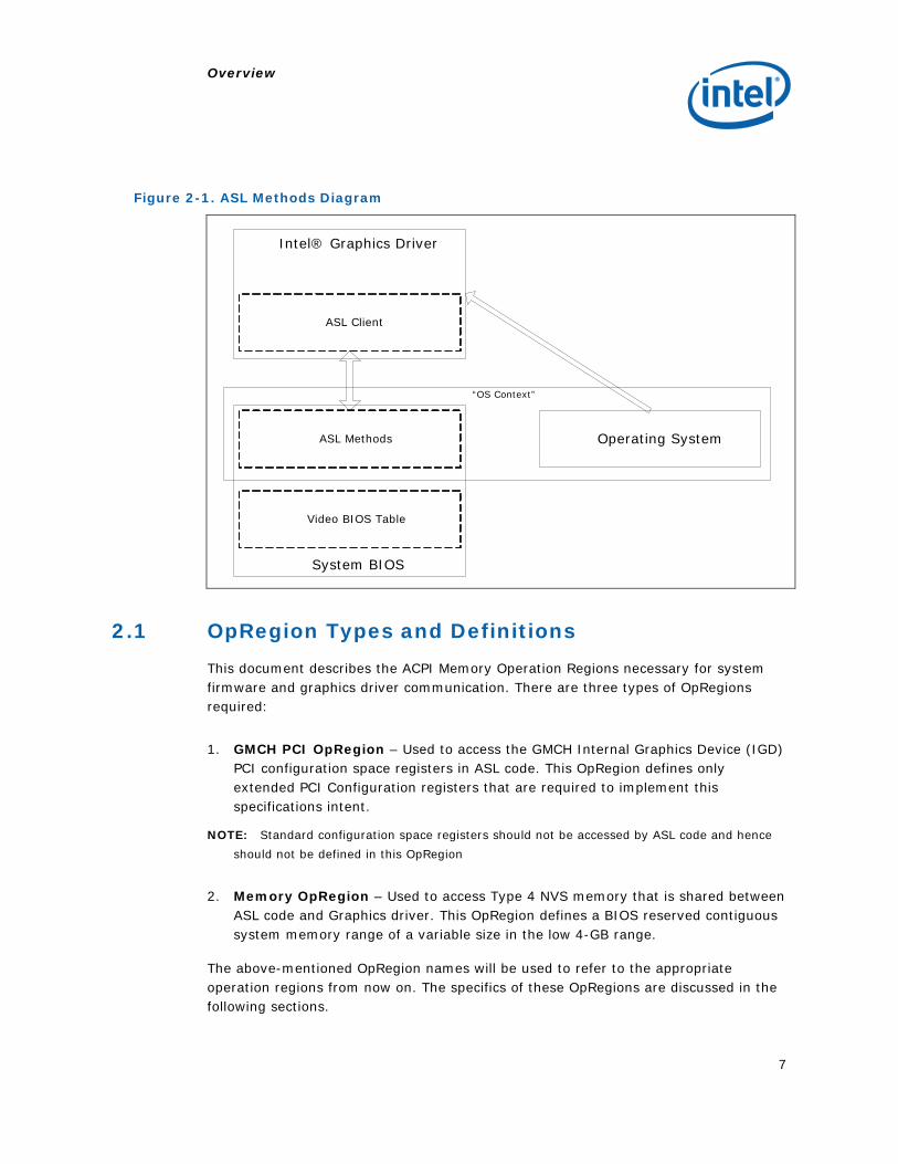
2 Overview The Integrated Graphics Device (IGD) OpRegion/Software SCI mechanism is a shared memory interface where the system BIOS reserves some physical pages in memory and labels them as custom Operation Regions (as defined by Advanced Configuration and Power Interface (ACPI) – Type 4 NVS). An ACPI specification compliant operating system would consider this region as reserved for ACPI framework and hence publishes this to the ACPI aware client drivers. Intel graphics drivers map this NVS memory region into the virtual address space giving all the interfacing software components (i.e., system BIOS, ASL methods, and Intel graphics drivers) access to the same shared memory region. These software components maintain this shared NVS memory region with system states allowing different user system control mechanisms to communicate and work together harmoniously. Intel Video BIOS does not have direct access to this shared memory region, but via interfaces to the system BIOS outside the scope of this document, it has access to the information it needs.
A second mechanism (Software SCI – Software System Control Interrupt) is introduced and detailed in this specification. Where the OpRegion is a passive memory block interface, the Software SCI is a dynamic client and server interface, the calling client being the Graphics drivers, and the server being an SCI handler and functions written in System BIOS ASL code. This new SCI mechanism is replaces the earlier SMI mechanism which was one our objectives listed earlier in Section 1.5. Basically, the Software SCI mechanism is a hardware interrupt that is activated by Intel graphics drivers passing control to an ASL interrupt handler giving platform generic drivers access to platform specific functionality without entering any SMM or other special processor mode.
These two mechanisms together make customer platform-specific functionality, user interfaces, and state data available to customer platform-generic graphics drivers and OS.
The Figure 2-1 depicts that the ASL methods are developed and distributed as part of the system firmware by the OEMs and IBVs but the execution model is in the context of OS solving the issue of wasted CPU cycles (and rendezvous times) in multi-processor environments.
Overview
7
Figure 2-1. ASL Methods Diagram
2.1 OpRegion Types and Definitions This document describes the ACPI Memory Operation Regions necessary for system firmware and graphics driver communication. There are three types of OpRegions required:
1. GMCH PCI OpRegion – Used to access the GMCH Internal Graphics Device (IGD) PCI configuration space registers in ASL code. This OpRegion defines only extended PCI Configuration registers that are required to implement this specifications intent.
NOTE: Standard configuration space registers should not be accessed by ASL code and hence should not be defined in this OpRegion
2. Memory OpRegion – Used to access Type 4 NVS memory that is shared between ASL code and Graphics driver. This OpRegion defines a BIOS reserved contiguous system memory range of a variable size in the low 4-GB range.
The above-mentioned OpRegion names will be used to refer to the appropriate operation regions from now on. The specifics of these OpRegions are discussed in the following sections.
System BIOS
“OS Context”
Intel® Graphics Driver
ASL Client
ASL Methods
Video BIOS Table
Operating System

Overview
8
2.2 GMCH PCI Config OpRegion Name ‘IGDP’
Type Any Access (DWORD preferred)
Offset IGD device ASLS, ASLE, and SWSCI registers minimally or entire extended space (40h-0FFh)
Size 0C0h bytes
Access Type Any Access (DWORD preferred)
Other Characteristics:
• Saved/Restored by graphics driver across power transitions and from S4.
Components Visible to:
• System BIOS, ASL code, and Graphics Driver.
• ACPI Kernel.
Components NOT Visible to:
• Video BIOS (limitation of “Real Mode”).
• All Other components not mentioned above.
When Created:
• System BIOS POST (S5->S0), S4->S0.
• System BIOS MUST initialize ASLS register with Memory OpRegion offset.
The following specific IGD registers are required to be defined specifically following registers in the non-standard space (40h-0FFh offsets):
Table 2-1. PCI OpRegion Registers
IGD PCI Config Space Register Usage GMCH PCI
Space Offset
Size (bits)
ASL Name
GMCH Reg.
Name
Description
GIVD MGGC0.IVD
IGFX Vga Disable
This Bit is used to denote if Device 2 can claim VGA Memory and IO Cycles
050h 16

Overview
9
IGD PCI Config Space Register Usage GMCH PCI
Space Offset
Size (bits)
ASL Name
GMCH Reg.
Name
Description
GUMA MGGC0.GMS
Graphics Mode Select
This field is used to select the amount of Main Memory that is pre-allocated to support the Internal Graphics device in VGA (non-linear) and Native (linear) modes.
050h 16
ASLE System Display Event
PCI interrupt trigger for System BIOS to send a command directly to Graphic driver
0E4h 32
SWSC SWSCI Software SCI GPE/SCI Trigger for Graphics driver to send a command to System BIOS.
0E8h 16
ASLS ASLS ASL Storage SW Scratch Register for System BIOS to pass Memory OpRegion physical address to driver. System BIOS is responsible for initializing this with the Memory OpRegion Offset.
0FCh 32
2.3 Memory OpRegion Name ‘IGDM’ or “IntelGraphicsMem” for OpRegion Header
Type System Memory, Cacheable Type 4 non-reclaimable Firmware Reserved Non-Executable
Offset Anywhere in system memory under 4 GB Note: This is a limitation of the 32-bit ASLS register in PCI configuration space.
Size Determined by System BIOS. Must be contiguous.
Access Type Any Access (DWORD preferred)
Other Characteristics:
• Non-Volatile Storage (NVS)
• Cacheable

Overview
10
• Non-Reclaimable (Type 4), Firmware Reserved
• Non-executable
Components Visible to:
• System BIOS, ASL, and Graphics Driver
• ACPI Kernel
Components NOT Visible to:
• Video BIOS (limitation of “Real Mode”)
• All Other components not mentioned above.
When Created:
• System BIOS POST (S5->S0), S4->S0
• System BIOS must initialize this region with zero’s
Only pertinent graphics data and data contained in this specification will be stored here. (Not for private use.)
§

OpRegion Memory Layout
11
3 OpRegion Memory Layout As explained in the 226H226HOverview chapter, the ACPI-based memory OpRegion is memory that is setup by the system BIOS and then shared between the interfacing software components (i.e., system BIOS, ASL code, and Graphics driver). It is reserved by the system BIOS and is a contiguous system memory range in the low 4-GB memory space.
System BIOS is responsible for indicating support for the OpRegion to the graphics driver. System BIOS indicates support via programming a valid (non-zero) physical address of the allocated Memory OpRegion in the ASLS PCI register. Conversely, a zero entry in the ASLS register indicates System BIOS does not support the OpRegion (i.e., is an older generation product and may support the legacy GMCH SMI method of communication).
The following table and sections in this chapter provides information on the memory OpRegion layout.
Table 3-1. OpRegion Layout
OpRegion Major Blocks Size (Bytes)
Offset (Bytes)
Access
OpRegion Header The OpRegion Header is used to identify a block of memory as the graphics driver OpRegion.
256 0 (0h)
SB = R/W ASL = R GD = R/W
Mailbox 1: Public ACPI Methods Mailbox 1 includes fields that support ACPI specification public method.
256 256 (100h)
SB = R/W ASL = R/W GD = R/W
Mailbox 2: Software SCI Interface Mailbox 2 is an interface to a private ACPI interrupt handler that is invoked by the graphics driver.
256 512 (200h)
SB = R/W ASL = R/W GD = R/W
Mailbox 3: BIOS to Driver Notification Mailbox 3 contains the ASLE driver interrupt mechanism and BIOS to Driver notification fields including power conservation and panel fitting fields.
256 768 (300h)
SB = R/W ASL = R/W GD = R/W
Mailbox 4: VBT The Video BIOS Table (VBT) is a block of customizable data that is originally built into the video BIOS binaries.
6144 (6K)
1024 (400h)
SB = W ASL = N/A GD = R

OpRegion Memory Layout
12
OpRegion Major Blocks Size (Bytes)
Offset (Bytes)
Access
Mailbox 5: BIOS to Driver Notification Extension Mailbox 5 supports BIOS to Driver event notification or data storage for BIOS to Driver data synchronization.
1024 (1K)
7168 (1C00h)
SB = W ASL = N/A GD = R
NOTE: All entries in the OpRegion are DWORD-aligned as far as their physical addresses go except for the internals of the VBT Image block. This means all addresses accessed by system BIOS are DWORD-aligned. The translated virtual address provided by OS to the graphics driver can be at any alignment.
3.1 OpRegion Header The OpRegion Header is always the first contiguous data block and is used to identify a memory address space as the start of the Memory OpRegion. It also contains other information that allows software to discover the memory OpRegion’s version, size, and supported mailboxes which will be needed to support future version of the structure.
Table 3-2. OpRegion Header Layout
OpRegion Header Fields Size (Bytes)
Offset (Bytes)
Access
SIGN OpRegion Signature = “IntelGraphicsMem”
16 0 (0h)
SB = WO ASL = n/a GD = R
SIZE OpRegion Size = 8 KB
4 16 (10h)
SB = WO ASL = n/a GD = R
OVER OpRegion Structure Version = v1.1 r0
4 20 (14h)
SB = WO ASL = n/a GD = R
SVER System BIOS Build Version
32 24 (18h)
SB = WO ASL = n/a GD = R
VVER Video BIOS Build Version
16 56 (38h)
SB = WO ASL = n/a GD = R
GVER Graphics Driver Build Version
16 72 (48h)
SB = R ASL = R GD = WO

OpRegion Memory Layout
13
OpRegion Header Fields Size (Bytes)
Offset (Bytes)
Access
MBOX Supported Mailboxes
4 88 (58h)
SB = WO ASL = n/a GD = R
DMOD Driver Model
4 92 (5Ch)
SB = RO ASL = RO GD = WO
PCON 4 96 (60h)
SB = WO ASL = n/a GD = RO
DVER GOP Version
32 100 (64h)
SB = WO ASL = n/a GD = RO
RM01 Reserved (must be zero)
124 132 (84h)
SB = WO ASL = n/a GD = n/a
The individual header fields are described below.
3.1.1 Signature (SIGN)
The ‘SIGN’ field is a case-sensitive string and is the primary identifier of the memory OpRegion. If the signature field is invalid, graphics driver will stop using OpRegion for any purpose and fail gracefully.
Table 3-3. Header SIGN Field
Offset (Bytes) Size (Bytes) Access
000h 010h SB = W, ASL = N/A, GD = R
Bits [127:0] - OpRegion Signature = “IntelGraphicsMem” These bits are a case-sensitive string and are the primary identifier of the memory OpRegion. If this field is invalid, the graphics driver will stop using OpRegion for any purpose and fail gracefully.
System BIOS Access (WO):
System BIOS writes this field once during its POST (normal boot and resume from hibernate).

OpRegion Memory Layout
14
ASL Code Access (N/A):
ASL code assumes the OpRegion is present and valid as it is part of the implementing system BIOS.
Driver Access (R):
Graphics driver reads this field once during its initialization prior to any other IGD OpRegion access. The intent is to ensure correctness of the Memory OpRegion. The driver validates this field during power resume times as well as a sanity check.
3.1.2 Size (SIZE)
The ‘SIZE’ field contains the size in KB of the entire OpRegion structure (including header). The size field should match the structure definition corresponding to its version indicated via OVER. If the size field is invalid, graphics driver will stop using OpRegion for any purpose and fail gracefully.
Table 3-4. Header SIZE Field
Offset (Bytes) Size (Bytes) Access
010h 004h SB = W, ASL = N/A, GD = R
Bits [31:0] - OpRegion Size = (incl. Header) in KB = 8 KB These bits contain the size in KB of the entire OpRegion structure (including header)
System BIOS Access (WO):
System BIOS writes this field once during its POST (normal boot and resume from hibernate).
ASL Code Access (N/A):
ASL code does not use this field.
Driver Access (R):
Graphics driver reads this field during initialization to get/verify the IGD OpRegion size. The intent is to ensure correctness of the OpRegion. The drivers validate this field during power resume times as well as a sanity check.
3.1.3 OpRegion Version (OVER)
The ‘OVER’ field holds the OpRegion/Software SCI design version and revision numbers.

OpRegion Memory Layout
15
Table 3-5. Header OVER Field
Offset (Bytes) Size (Bytes) Access
014h 004h SB = W, ASL = N/A, GD = R
Bits [31:16] - Major Version Number BCD Integer representing the major version of the OpRegion/SWSCI Interface
Bits [23:0] - Minor Version Number BCD Integer representing the minor version of the OpRegion/SWSCI Interface
Chipset OVER Mailbox 1 Mailbox 2 Mailbox 3 Mailbox 5
Skylake Mobile 3.0 r0 Supported Supported Supported Optional
Skylake Desktop 3.0 r0 Supported Supported Supported Optional
The fields are supported in Version 2.0. Both Driver and BIOS are sticking with version 2.0 currently and even the new fields are supported even 2.0 onwards.
If the Driver or BIOS is having older version, the respective callbacks wouldn’t be set and hence no problem with backward compatibility.
System BIOS Access (WO):
System BIOS writes this field once during its POST (normal boot and resume from hibernate). The system BIOS only needs to support a single version of OpRegion/Software SCI mechanism. The version of the OpRegion/Software SCI mechanism in this document is version 1.1 revision 0.
ASL Code Access (N/A):
ASL code does not use this field.
Driver Access (R):
Graphics driver reads this field once during its initialization. The driver should support all documented versions for backwards compatibility support, but at run-time, support the exact version that System BIOS supports which is indicated via this field. If the version field is invalid, the driver will stop using OpRegion for any purpose and fail gracefully.
3.1.4 System BIOS Version (SVER)
The ‘SVER’ field holds the System BIOS version number for diagnostic purposes.

OpRegion Memory Layout
16
Table 3-6. Header SVER Field
Offset (Bytes) Size (Bytes) Access
018h 020h SB = W, ASL = N/A, GD = R
Bits [255:0] - System BIOS Version System BIOS version is stored as an ASCII string
System BIOS Access (WO):
System BIOS writes this field once during its POST (normal boot and resume from hibernate).
ASL Code Access (N/A):
ASL code does not use this field.
Driver Access (R):
Graphics driver only uses this field for diagnostic purposes and is not used in production software.
3.1.5 Video BIOS Version (VVER)
The ‘VVER’ field holds the Video BIOS version number. This version number is used by Intel CUI control panel application to display the Video BIOS version.
Table 3-7. Header VVER Field
Offset (Bytes) Size (Bytes) Access
038h 010h SB = W, ASL = N/A, GD = R
Bits [127:0] - Video BIOS Build Version Video BIOS version is stored as an ASCII string. This field is filled when IGD is primary or secondary, and the intent is for Intel CUI control panel application to display the Video BIOS version. This could also be used for diagnostic purposes to aid debugging.
System BIOS Access (WO):
System BIOS writes this field once during its POST (normal boot and resume from hibernate). System BIOS obtains the Video BIOS version information as described in Section 5.3.4
ASL Code Access (N/A):
ASL code does not use this field.
OpRegion Memory Layout
17
Driver Access (R):
Graphics driver reads this field upon request from Intel CUI to determine Video BIOS information.
3.1.6 Graphics Driver Version (GVER)
The ‘GVER’ field holds the Graphics driver version number for diagnostic purposes.
Table 3-8. Header GVER Field
Offset (Bytes) Size (Bytes) Access
048h 010h SB = R, ASL = R, GD = W
Bits [127:0] - Graphics Driver Build Version Graphics driver build version is stored as an ASCII string. This field is filled with the version of graphics driver (when IGD is primary or secondary) and the intent is for diagnostic purposes only to aid debugging.
System BIOS Access (R):
System BIOS uses this field for debug purposes only.
Warning: OEMs/IBVs are at their own risk as Intel reserves the right to change the versioning policy and thereby the associated version numbers or revisions.
ASL Code Access (R):
ASL code may read this field to incorporate a workaround for particular driver builds.
Driver Access (WO):
Graphics driver writes this field once during its initialization during normal boot.
3.1.7 Supported Mailboxes (MBOX)
The ‘MBOX’ field identifies what mailboxes are supported.
Table 3-9. Header MBOX Field
Offset (Bytes) Size (Bytes) Access
058h 004h SB = W, ASL = N/A, GD = W

OpRegion Memory Layout
18
Offset (Bytes) Size (Bytes) Access
Bits [31:5] - Reserved Reserved (must be zero)
Bits [4] - Mailbox 5: BIOS to Driver Notification Extension 0 = No support for mailbox and its features 1 = Support for mailbox and its features
Bits [3] - Mailbox 4: VBT 1 = Must be supported
Bits [2] - Mailbox 3: BIOS to Driver Notification 0 = No support for mailbox and its features 1 = Support for mailbox and its features
Bits [1] - Mailbox 2: Software SCI 0 = No support for mailbox and its features 1 = Support for mailbox and its features
Bits [0] - Mailbox 1: Public ACPI Methods 0 = No support for mailbox and its features 1 = Support for mailbox and its features
NOTE: Support for the VBT mailbox is required and therefore does have a mailbox support bit.
System BIOS Access (WO):
System BIOS writes this field once during its POST (normal boot and resume from hibernate).
ASL Code Access (N/A):
Not used by ASL code.
Driver Access(R):
Graphics driver reads at any time to determine mailbox support.
3.1.8 Driver Model (DMOD)
The ‘DMOD’ field indicates the type/model of Graphics Driver currently loaded. Graphics driver will update this field once the driver is successfully loaded. BIOS can read this field to make decision based on the type of Graphics Driver loaded. On driver unload, graphics driver needs to make DMOD = 0 to indicate to the System BIOS that no graphics driver is loaded now.
Note: This field is supported from OpRegion Version (refer to Section 3.1.3) = 2.0 forward.

OpRegion Memory Layout
19
Table 3-10. Header DMOD Field
Offset (Bytes) Size (Bytes) Access
05Ch 004h SB = R, ASL = R, GD = W
Bits [31:0] – Driver Model 00h – Graphics Driver not loaded 01h – XPDM Driver loaded 02h – WDDM Driver loaded All other values are reserved
System BIOS Access (RO):
System BIOS can read this field anytime.
ASL Code Access (RO):
ASL codes can read this field and may take different paths for different driver model when needed.
Driver Access (WO):
Graphics driver writes to this field on driver load/unload.
3.1.9 Platform Configuration (PCON)
This field indicates the Platform Configuration Information. Details of bit definitions are as below. The field is populated by BIOS and Driver reads it.
Table 3-11. Header PCON Field
Offset (Bytes) Size (Bytes) Access
060h 004h SB = W, ASL = N/A GD = R

OpRegion Memory Layout
20
Offset (Bytes) Size (Bytes) Access
Bits [31:9] – Reserved (Must be Zero) Bits[8] – External Gfx Adapter Field valid 0 = External Gfx Adapter field is Not valid 1 = External Gfx Adapter field is valid
Bits[7] – External Gfx Adapter 0 = No External Gfx Adapter 1 = External Gfx Adapter Detected and Available
Bits[6] – ISCT Capability Support Field valid 0 = Platform ISCT Capability Field is Not valid 1 = Platform ISCT Capability Field is valid
Bits[5] – ISCT Support Field 0 = Platform is not ISCT capable 1 = Platform is ISCT capable
Bits[4] – Audio Type Support Field valid 0 = Audio type support field is not valid 1 = Audio type support field is valid
Bits[3:2] – Audio Type Support 0 = No Audio Supported 1 = High Definition Audio Support 2 = Low Power Audio Support 3 = Rsvd
Bits[1] – Platform Connected Standby Capability Support Field valid 0 = Platform Connected Standby Capability field is not valid 1 = Platform Connected Standby Capability field is valid
Bits[0] – Platform Connected Standby Capability Support 0 = Platform is Connected Standby Capable 1 = Platform is not Connected Standby Capable
System BIOS Access (W):
System BIOS writes to this field during boot
ASL Code Access (N/A):
Not used by ASL code.
Driver Access (RO):
Graphics driver will read from this field

OpRegion Memory Layout
21
3.1.10 GOP Version (DVER)
This field is filled with the version of GOP (when IGD is primary or secondary) and the intent is for Intel CUI control panel application to display the GOP version. This could also be used for diagnostic purposes to aid debugging. The version info is filled with character info terminated by a NULL character. Gfx Driver will read through the Link to Memory OpRegion Layout
Table 3-12. Header DVER Field
Offset (Bytes) Size (Bytes) Access
064h 020h SB = W, ASL = N/A GD = R
GOP Build Version = Version (Wide Character string)
System BIOS Access (W):
This field is written once by the System BIOS during its POST (normal boot and resume from hibernate).
ASL Code Access (N/A):
Not used by ASL code.
Driver Access (RO):
Graphics driver reads this field upon request from Intel CUI to determine GOP Version information
3.2 Mailbox 1: Public ACPI Methods This mailbox supports ACPI events that results in Public ASL method execution either in GFX scope or outside of GFX scope with graphics implications (e.g., Docking/ Undocking events). A public method is one that’s documented in the ACPI specification.
Table 3-13. OpRegion Mailbox 1 (Public ACPI Methods) Layout
Mailbox 1 (Public ACPI Methods) Fields Size (Bytes)
Offset (Bytes)
Access
DRDY Driver Readiness
4 0 256
(100h)
SB = R ASL = R GD = W

OpRegion Memory Layout
22
Mailbox 1 (Public ACPI Methods) Fields Size (Bytes)
Offset (Bytes)
Access
CSTS STATUS
4 4 260
(104h)
SB = W ASL = R GD = R/W
CEVT Current Event
4 8 264
(108h)
SB = R/W ASL = R/W GD = R
RM11 Reserved (must be zero)
20 12 268
(10Ch)
SB = WO ASL = n/a GD = n/a
DIDL Supported Display Devices ID List (_DOD)
32 8 DWORDs
32 288
(120h)
SB = R ASL = R GD = R/W
CPDL Currently Attached (or Present) Display Devices List
32 8 DWORDs
64 320
(140h)
SB = R ASL = R GD = R/W
CADL Currently Active Display Devices List (_DCS)
32 8 DWORDs
96 352
(160h)
SB = R ASL = R GD = R/W
NADL Next Active Devices List (_DGS use)
32 8 DWORDs
128 384
(180h)
SB = R/W ASL = R/W GD = R/W
ASLP ASL Sleep Time Out
4 160 416
(1A0h)
SB = R ASL = R GD = W
TIDX Toggle Table Index
4 164 420
(1A4h)
SB = R/W ASL = R/W GD = R
CHPD Current Hot Plug Enable Indicator
4 168 424
(1A8h)
SB = R ASL = R GD = R/W
CLID Current Lid State Indicator
4 172 428
(1ACh)
SB = R/W ASL = R/W GD = R
CDCK Current Docking State Indicator
4 176 432
(1B0h)
SB = R/W ASL = R/W GD = R

OpRegion Memory Layout
23
Mailbox 1 (Public ACPI Methods) Fields Size (Bytes)
Offset (Bytes)
Access
SXSW Request ASL to issue Display Switch notification on Sx State resume
4 180 436
(1B4h)
SB = R/W ASL = R/W GD = W
EVTS Events Supported by ASL (Diagnostic Purposes Only)
4 184 440
(1B8h)
SB = R/W ASL = R/W GD = R
CNOT Current OS Notifications (Diagnostic Purposes Only)
4 188 444
(1BCh)
SB = R/W ASL = R/W GD = R/W
NRDY Reasons for DRDY = 0 or failure conditions in CSTS (Diagnostic Purposes Only)
4 192 448
(1C0h)
SB = R ASL = R GD = W
DID2 Extended Supported Devices ID List (DOD)
28 196 452
(1C4h)
SB = R ASL = R
GD = R/W
CPD2 Ex8tended Attached Display Devices List
28 224 480
(1E0h)
SB = R ASL = R
GD = R/W
RM12 Reserved (must be zero)
4 252 508
(1FCh)
SB = WO ASL = n/a GD = n/a
NOTES: 1. The access level specified in this table for SBIOS & Driver is a suggested guideline only.
No enforcement will be made by the Graphics Driver or the Operating System. 2. Optional fields are labeled as “Diagnostic” and are only for debug/diagnostic purposes.
It is strongly recommended to support them. 3. Offset column: The first number is relative to Mailbox 1, and the second number is
relative to the start of the OpRegion. 4. To simplify access, it may be necessary to identify the individual elements in the
Display Device List fields DIDL, CPDL, CADL, and NADL.
The individual mailbox fields are described below.
3.2.1 Driver Ready (DRDY)
The ‘DRDY’ field indicates whether graphics driver is ready to process ACPI Video Extensions notifications from System BIOS.

OpRegion Memory Layout
24
Table 3-14. Mailbox 1 DRDY Field
Offset (Bytes) Size (Bytes) Access
100h 004h SB = R, ASL = R, GD = W
Bits [31:0] - Driver Readiness These bits indicate whether graphics driver is ready to process ACPI Video Extensions notifications from System BIOS 00000000h = Driver not ready for Video Extensions calls 00000001h = Driver is ready for Video Extensions calls 00000002h – 0FFFFFFFFh = Reserved
System BIOS Access:
Writes/Reads – Not used by system BIOS POST code.
Writes – Only read by system BIOS ASL code.
Reads – System BIOS ASL code reads this field before a) sending any notifications to the driver or b) handling ACPI Video Extensions. If graphics driver is not ready, NRDY may optionally indicate the reason why graphics driver is not ready.
System BIOS ASL code has options if graphics driver is loaded but not ready:
1. Fail the ACPI event processing gracefully without further GFX notifications. Where OS notifications are mandatory, they still need to be issued e.g., Lid event.
2. Sleep/Poll DRDY for driver readiness, Timeout if driver not ready after a specified interval of time
If Graphics driver is not loaded yet but OSPM is ready, System BIOS can fail ACPI Video Extensions gracefully.
Driver Access:
Writes – Graphics driver sets this field after a successful loading, initialization, or resume from sleep states (S3 & S4). Graphics driver resets the field to 00h in cases of entering power management sleep states (S3 & S4). Graphics driver must also use this field to indicate the System BIOS in cases it is not ready to handle the ACPI Video Extensions. Graphics driver is strongly encouraged to provide reason via NRDY.
Reads – Driver does not read this field
Relevant ACPI Methods:
All ACPI Video Extensions methods; See the ACPI Specification, Video Extensions, for details.
Relevant ACPI OS Notifications:

OpRegion Memory Layout
25
All ACPI Video Extensions notifications; See the ACPI specification, Video Extensions, for details.
3.2.2 Notification Status (CSTS)
The ‘CSTS’ field provides a graphics notification progress indicator. This serves as a handshake mechanism between System BIOS ASL code and Graphics driver in order to process a specific graphics notification.
Table 3-15. Mailbox 1 CSTS Field
Offset (Bytes) Size (Bytes) Access
104h 004h SB = W, ASL = R, GD = R/W
Bits [31:0 - Notification Status These bits provide a graphics notification progress indicator. This serves as a handshake mechanism between System BIOS ASL code and Graphics driver in order to process a specific graphics notification. 00000000h = Success (Driver) 00000001h = Failure (Driver) 00000002h = Pending, Transaction (Driver) 00000003h = Dispatched, Transaction (ASL) 00000004h – 0FFFFFFFFh = Reserved
System BIOS Access:
Writes/Reads – Not used by system BIOS POST code.
Writes – System BIOS ASL code can only write a “Dispatched” value to this field. This write should be done prior to any graphics notification issued by System BIOS ASL code and only if the current status is Success or Failure.
Reads – System BIOS ASL code can read this field anytime. System BIOS ASL code sleeps/polls this field for a “Success”/“Failure” status before issuing another notification or exiting the method.
Note: In earlier BIOS reference code, prior to issuing an ACPI notification, ASL code polls CSTS for time “t” when it is set to “Dispatched”, and returns failure on timeout. This could cause all subsequent events to fail if an event is not received or processed by the OS or the driver. It is recommended that the check of CSTS be removed. The second option is to check for CSTS for time “t” when it is set to “Dispatched”, and send another notification on timeout regardless of the CSTS value.

OpRegion Memory Layout
26
Driver Access:
Writes – Graphics driver can initiate writes to this field only if the value is “Dispatched.” Subsequent write values can be “Pending” followed by “Success” or “Failure.” If a failure condition occurs, driver can optionally provide the reason via NRDY.
Reads – Graphics driver can read this field anytime. This field is typically read by the graphics driver on any graphics notification from System BIOS ASL code/OSPM. Driver determines the origin of the Driver call to be ASL if the value read back is “Dispatched.” Driver would then acknowledge receipt of the notification by setting “Pending” status before processing the notification. Upon completion, Driver would either set “Success” or “Failure.” Driver shall not process the notification if ‘CSTS’ is not equal to dispatched (i.e., CSTS != Dispatched).
Relevant ACPI Methods:
All ACPI Video Extensions methods; See the ACPI specification, Video Extensions, for detail8s.
Relevant ACPI OS Notifications:
All ACPI Video Extensions notifications; See the ACPI specification, Video Extensions, for details.

OpRegion Memory Layout
27
3.2.3 Current Event (CEVT)
The intent of the ‘CEVT’ field is to notify the driver of the event and for the driver to apply appropriate persistence if necessary.
Table 3-16. Mailbox 1 CEVT Field
Offset (Bytes) Size (Bytes) Access
108h 004h SB = R/W, ASL = R/W, GD = R
Bits [31:3] - Reserved Must be zero
Bits [2] - Dock/Undock This field indicates if the current ACPI Video Extensions Dock/Undock event trigger is being serviced 0 = No Dock/Undock Event 1 = Dock/Undock Event
Bits [1] - Lid Open/Close This field indicates if the current ACPI Video Extensions Lid Open/Close event trigger is being serviced 0 = No Lid Open/Close Event 1 = Lid Open/Close Event
Bits [0] - Display Switch Hot-Key Press This field indicates if the current ACPI Video Extensions Display Switch Hot-Key Press event trigger is being serviced 0 = No Display Switch Hot-Key Press Event 1 = Display Switch Hot-Key Press Event
NOTE: Only one bit of this field shall be set at any one time.
System BIOS Access:
Writes – System BIOS POST or ASL code can only write one of the event values at a time.
Reads – System BIOS POST or ASL code can read this field anytime if required. The intent is for System BIOS to serialize or block any potential back to back user event triggers.
Note: System BIOS needs to update CEVT only for Notify(VGA,0x80) since this notification is overloaded for multiple ACPI events (hotkey, lid, dock) in Microsoft Windows* XP.
Note: It is not necessary for the System BIOS to clear CEVT after sending the notifications, since the driver only considers the event variable when the status flag is set to “Dispatched”. Furthermore attempting to clear CEVT will likely cause a 750-ms delay in processing.

OpRegion Memory Layout
28
Driver Access:
Writes – Graphics driver cannot write to this field.
Reads – Graphics driver typically reads this field in response to an OS call to switch displays or re-enumerate display devices so that it can apply appropriate persistence.
Relevant ACPI Methods:
All ACPI Video Extensions methods; See the ACPI specification, Video Extensions, for details.
Relevant ACPI OS Notifications:
All ACPI Video Extensions notifications; See the ACPI specification, Video Extensions, for details.
3.2.4 Supported Display Devices ID List (DIDL)
The ‘DIDL’ field indicates what display devices are supported by the platform and therefore enumerable by the graphics driver. A maximum of 8 devices are assumed supportable on a given platform and enumerable by the graphics driver. Graphics driver detects/determines devices during its initialization and prior to the first monitor enumeration call it receives from the OS. System BIOS uses this list (as is) to package a list of IDs and return that list in _DOD method invocation. In the event of _DOD getting invoked by OSPM prior to graphics driver initializing this list (i.e., all IDs are 0), System BIOS _DOD method should return no enumerable connectors to OSPM.
Table 3-17. Mailbox 1 DIDL Field
Bit Fields Description
DWORD [7] ACPI ID 7
DWORD [6] ACPI ID 6
DWORD [5] ACPI ID 5
DWORD [4] ACPI ID 4
DWORD [3] ACPI ID 3
DWORD [2] ACPI ID 2
DWORD [1] ACPI ID 1
DWORD [0] ACPI ID 0

OpRegion Memory Layout
29
Extended DID2
Bit Fields Description
DWORD [14] ACPI ID 14
DWORD [13] ACPI ID 13
DWORD [12] ACPI ID 12
DWORD [11] ACPI ID 11
DWORD [10] ACPI ID 10
DWORD [9] ACPI ID 9
DWORD [8] ACPI ID 8
NOTES: 1. In case of less than 15 IDs, Graphics driver should terminate the list with 0 after the
last ID. 2. The Extended DIDL field is supported from OpRegion Version (refer OVER) = 3.0
onwards.
Driver and BIOS are sticking to 2.0 version itself and hence currently OVER would still be 2.0 where these fields would be working. If the Driver or BIOS is having older version, the respective fields would be 0 and hence no problem with backward compatibility.
Table 3-18. Mailbox 1 DIDL Field ACPI ID
Offset (Bytes) Size (Bytes) Access
120h 020h SB = R, ASL = R, GD = R/W
01C4h 01Ch SB = R, ASL = R, GD = R/W
Bits [31:16] - ACPI ID The ACPI ID details can be found in Section 5.2.2.
System BIOS Access:
Writes – System BIOS POST or ASL code should not write to these fields.
Reads – System BIOS POST or ASL code can read this field anytime if required. The intent is for System BIOS to package this list w/o modification when it’s _DOD method is invoked by OSPM.
Driver Access:
Writes – Graphics driver writes to this field once during its initialization after determining platform supported connectors.

OpRegion Memory Layout
30
Reads – Graphics driver typically can read this field as sanity check during monitor enumeration call from the OS.
Relevant ACPI Methods:
_DOD
Relevant ACPI OS Notifications:
Notify (VGA, 0) – Graphics device enumeration.
Notify (VGA, 0x81) – Some OS implementations cause serious side effects and hence System BIOS implementations are advised to avoid this.
Notify (\_SB.PCI0, 0) – PCI Bus 0 wide enumeration.
3.2.5 Currently Attached Display Devices List (CPDL)
The ‘CPDL’ field indicates what display devices (monitors) are currently connected to the previously enumerated connectors. A maximum of eight monitors are assumed supportable on a given platform and enumerable by the graphics driver. Graphics driver detects/determines monitors at various times in response to different triggers: OS calls, Hot-plug of a monitor, Boot/Resume times etc.
For description on _DOD ID formats, refer to Section 5.2.2
Table 3-19. Mailbox 1 CPDL Field
Bit Fields Description
DWORD [7] ACPI ID 7
DWORD [6] ACPI ID 6
DWORD [5] ACPI ID 5
DWORD [4] ACPI ID 4
DWORD [3] ACPI ID 3
DWORD [2] ACPI ID 2
DWORD [1] ACPI ID 1
DWORD [0] ACPI ID 0

OpRegion Memory Layout
31
Extended CPD (CPD2)
Bit Fields Description
DWORD [14] ACPI ID 14
DWORD [13] ACPI ID 13
DWORD [12] ACPI ID 12
DWORD [11] ACPI ID 11
DWORD [19] ACPI ID 10
DWORD [9] ACPI ID 9
DWORD [8] ACPI ID 8
NOTE: In case of less than 15 IDs, Graphics driver should terminate the list with 0 after the last ID.
Table 3-20. Mailbox 1 CPDL Field ACPI ID
Offset (Bytes) Size (Bytes) Access
140h 020h SB = R ASL = R, GD = R/W
1E0h 01Ch SB = R ASL = R, GD = R/W
Bits [31:16] - ACPI ID The ACPI ID details can be found in Section 5.2.2, Video Extensions Reference.
System BIOS Access:
Writes – System BIOS POST or ASL code should not write to these fields.
Reads – System BIOS POST or ASL code can read this field anytime if required. The intent is for System BIOS to optionally determine what display devices to switch to say for a hot-key display switch press. Usually, this determination is done by graphics driver based on OEM settings via VBT. System BIOS however can override the driver determination.
Driver Access:
Writes – Graphics driver writes to this field on every monitor detection process.
Reads – Graphics driver can read this field to update NADL.
Relevant ACPI Methods:
_DGS – System BIOS can optionally use this field to determine what to return via _DGS

OpRegion Memory Layout
32
Relevant ACPI OS Notifications:
Notify (VGA, 0x80) – Graphics display device switch
NOTE: The Extended CPD (CPD2) field is supported from OpRegion Version (refer OVER) = 3.0 onwards.
Driver and BIOS are sticking to 2.0 version itself and hence currently OVER would still be 2.0 where these fields would be working. If the Driver or BIOS is having older version, the respective fields would be 0 and hence no problem with backward compatibility.
3.2.6 Currently Active Display Devices List (CADL)
The ‘CADL’ field indicates what display devices (monitors) are currently active. A maximum of eight monitors are assumed active on a given platform. The IDs should be the same as the enumerated monitor/connector IDs. Graphics driver determines active monitors during mode set times and during boot.
Table 3-21. Mailbox 1 CADL Field
Bit Fields Description
DWORD [7] ACPI ID 8
DWORD [6] ACPI ID 7
DWORD [5] ACPI ID 6
DWORD [4] ACPI ID 5
DWORD [3] ACPI ID 4
DWORD [2] ACPI ID 3
DWORD [1] ACPI ID 2
DWORD [0] ACPI ID 1
NOTE: In case of less than 8 IDs, Graphics driver should terminate the list with 0 after the last ID.
Table 3-22. Mailbox 1 CADL Field ACPI ID
Offset (Bytes) Size (Bytes) Access
160h 020h SB = R ASL = R, GD = R/W
Bits [31:16] - ACPI ID The ACPI ID details can be found in Section 5.2.2, Video Extensions Reference.

OpRegion Memory Layout
33
System BIOS Access:
Writes – System BIOS POST and ASL code should not write to these fields.
Reads – System BIOS can read this field anytime to support _DCS. Optionally, System BIOS can use this information to determine what display devices to switch to say for a hot-key display switch press. Usually, this determination is done by graphics driver based on OEM settings via VBT. System BIOS however can override the driver determination.
Driver Access:
Writes – Graphics driver writes to this field on every mode set process and during boot.
Reads – Graphics driver can read this field to update NADL.
Relevant ACPI Methods:
_DCS
Relevant ACPI OS Notifications:
Notify (VGA, 0x80) – Graphics display device switch.
3.2.7 Next Active Display Devices List (NADL)
The ‘NADL’ field indicates what display devices (monitors) are to switch to next on a subsequent hot-key or lid event display switch. A maximum of eight monitors are assumed switchable to on a given platform. The IDs should be the same as the enumerated monitor/connector IDs. Graphics driver determines which monitors to switch to based on selected toggle table (1 of 4) indicated via ‘TIDX’ by ASL code.
Graphics driver should update this field after any display changes or hot-plug/unplug. ASL can override the driver selection if ASL maintains the toggle table internally i.e., outside of VBT based toggle tables.
Note: The value in TIDX must be non-zero in order for the driver to update the NADL field.
Table 3-23. Mailbox 1 NADL Field
Bit Fields Description
DWORD [7] ACPI ID 8
DWORD [6] ACPI ID 7
DWORD [5] ACPI ID 6
DWORD [4] ACPI ID 5
DWORD [3] ACPI ID 4
OpRegion Memory Layout
34
Bit Fields Description
DWORD [2] ACPI ID 3
DWORD [1] ACPI ID 2
DWORD [0] ACPI ID 1
Note: In case of less than 8 IDs, Graphics driver should terminate the list with 0 after the last ID.
Table 3-24. Mailbox 1 NADL Field ACPI ID
Offset (Bytes) Size (Bytes) Access
180h 020h SB = R/W ASL = R/W GD = R/W
Bits [31:16] - ACPI ID The ACPI ID details can be found in Section 5.2.2, Video Extensions Reference.
System BIOS Access:
Writes – System BIOS POST or ASL code should write to these fields if it wishes to override the driver determined next device list.
Reads – System BIOS POST or ASL code can read this field anytime to support _DGS. System BIOS can either use this list as is to determine what display devices to switch to say for a hot-key display switch press or override it with its own.
Driver Access:
Writes – Graphics driver writes to this field on every mode set process, any change in attached display devices and during boot/resume.
Reads – Graphics driver can read this field as a sanity check on display switch call from OS.
Relevant ACPI Methods:
_DGS
Relevant ACPI OS Notifications:
Notify (VGA, 0x80) – Graphics display device switch

OpRegion Memory Layout
35
3.2.8 ASL Sleep Time-out (ASLP)
The ‘ASLP’ field indicates suggests maximum sleep/poll time that ASL methods can use while awaiting driver handshaking of event processing. The time (in Milliseconds) is programmed one-time by driver during OpRegion initialization. ASL may use this value to sleep before issuing another graphics notification or proceeding with the rest of the method. ASL SHOULD NOT sleep on ASL notifications entirely consumed by OS (i.e., graphics driver does not receive any calls).
Table 3-25. Mailbox 1 ASLP
Offset (Bytes) Size (Bytes) Access
1A0h 004h SB = R ASL = R GD = W
Bits [31:0] - ASL Sleep Time Out These bits provide the maximum sleep time in milliseconds (Integer decimal). 00000000h = No driver suggestion. ASL code to use internal default. 00000001h - 0FFFFFFFFh = Driver suggested sleep/poll time.
System BIOS Access:
Writes/Reads – System BIOS POST code does not use this field.
Writes – System BIOS ASL code should not write to this field.
Reads – System BIOS ASL can read this field anytime to support sleep in its methods. System BIOS can either use a single sleep instruction for the specified amount of time or break the sleep interval into time slices (recommended) and periodically check for driver status in between.
Note: It is very important for ASL code to not be placed in a sleep mode for long amounts of time between notifications to OSPM; therefore the use of the ASL Sleep Time Out should be limited only to methods where it is absolutely necessary.
Driver Access:
Writes – Graphics driver writes to this field once during boot process.
Reads – Graphics driver should not read this field.
Relevant ACPI Methods:
All methods.
Relevant ACPI OS Notifications:
Notify (VGA, 0x80) – Graphics display device switch.

OpRegion Memory Layout
36
3.2.9 Toggle Table Index (TIDX)
The ‘TIDX’ is the ASL specified Toggle Table index that needs to be used by graphics driver to determine the next display device combination. ASL can dynamically change this value prior to sending to a display switch notification to OS. This is for handling multiple hot-key designs.
Note: The value in TIDX must be non-zero in order for the driver to update the NADL field.
Table 3-26. Mailbox 1 TIDX Field
Offset (Bytes) Size (Bytes) Access
1A4h 004h SB = R/W ASL = R/W GD = R
Bits [31:0] - Toggle Table Index These bits provide the display device toggle table to use when finding the next display device for a display toggle hot key (Integer decimal) 00000000h = Use Toggle Table 1 00000001h = Use Toggle Table 2 00000002h = Use Toggle Table 3 00000003h = Use Toggle Table 4 All other values = Reserved
System BIOS Access:
Writes – System BIOS POST or ASL code writes to this field. System BIOS should send a display switch notification to OS before writing a new value in this field.
Reads – System BIOS POST or ASL code can read this field.
Driver Access:
Writes – Graphics driver should not write into this field.
Reads – Graphics driver reads this field.
Relevant ACPI Methods:
All methods.
Relevant ACPI OS Notifications:
Notify (VGA, 0x80) – Graphics display device switch.

OpRegion Memory Layout
37
3.2.10 Current Hot Plug Enable Indicator (CHPD)
The ‘CHPD’ field indicates if graphics driver currently supports Hot Plug monitor detection i.e., Monitor attachment/detachment causes IGD PCI Interrupt generation. Hot plug support can be disabled and re-enabled dynamically based on operating conditions. To avoid latencies incurred by display enumeration process, ASL code should trigger re-enumeration notification (notify (VGA, 0)) only if Hot-Plug support is disabled.
This Hot Plug Enable Indicator is not a representation state of each and every display device type or encoder in the platform. Rather this is a global flag and the Driver should set this field if at least one display device or encoder in the platform does not support hot-plug feature or have its hot-plug feature disabled.
OS Dependency: System BIOS should trigger re-enumeration notification only for those operating systems that do not support Hot-Plug based re-enumeration for example, Microsoft Windows* 2000 and Windows XP. Re-enumeration trigger logic in System BIOS MUST be disabled for all the Operating Systems supporting Hot-Plug (e.g., Windows* Longhorn and above) but can handle the Hot-Plug disabled scenarios.
Table 3-27. Mailbox 1 CHPD Field
Offset (Bytes) Size (Bytes) Access
1A8h 004h SB = R ASL = R GD = W
Bits [31:0] - Current Hot Plug Enable Indicator These bits indicate if graphics driver currently supports Hot Plug monitor detection i.e., Monitor attachment/detachment causes IGD PCI Interrupt generation. 00000000h = Hot Plug support disabled 00000001h = Hot Plug support enabled 00000002h - 0FFFFFFFFh = Reserved
System BIOS Access:
Writes – System BIOS POST or ASL code should not write into this field.
Reads – System BIOS POST or ASL code can read this field.
Driver Access:
Writes – Graphics driver writes into this field.
Reads – Graphics driver reads this field.
Relevant ACPI Methods:

OpRegion Memory Layout
38
All methods.
Relevant ACPI OS Notifications:
Notify (VGA, 0x0) – Display re-enumeration.
3.2.11 Current Lid State Indicator (CLID)
The ‘CLID’ field indicates whether Lid is currently open or closed. Lid state updates rules:
• Prior to graphics driver load to provide the initial state of the lid to the driver.
• After graphics driver load every time Lid is opened or closed i.e., on a Lid event.
For post graphics driver load scenario, Lid State change also needs to be notified to Graphics driver prior to notify (VGA, 80). While ASLE interrupt would be 1 mechanism, the suggested mechanism is notify (VGA, 0) to perform re-enumeration. This is because graphics driver anyway has to perform a re-enumeration to inform OS of LFP availability/unavailability.
Graphics driver during enumeration also sets up the ‘Next Active Display Devices’ entry accordingly. ASL code should disregard the ‘Current Hot Plug Enable’ indicator in this case.
Also, since GMCH can support 2 LFP devices, Lid states need to be reported at any point of time for each of the LFP devices supported via _DOD. Refer to _DOD ACPI Device ID’s doc for information on how to determine ACPI ID’s for Integrated and External LFP.
Table 3-28. Mailbox 1 CLID Field
Offset (Bytes) Size (Bytes) Access
1ACh 004h SB = R/W ASL = R/W GD = R
Bits [31:2] - Reserved Must be zero
Bits [1:0] - LFP Lid State These bits contain the lid state of an integrated LFP 00 = All LFP lids are closed 01 = Integrated LFP lid is open 10 = External LFP lid is open 11 = Both Integrated LFP and External LFP lid are open

OpRegion Memory Layout
39
System BIOS Access:
Writes – System BIOS POST or ASL code writes this field.
Reads – System BIOS POST or ASL code can read this field.
Driver Access:
Writes – Graphics driver should not write into this field.
Reads – Graphics driver reads this field.
Relevant ACPI Methods:
All methods.
Relevant ACPI OS Notifications:
Notify (VGA, 0x80) - Graphics display switch. Notify (VGA, 0x0) - Display re-enumeration.
3.2.12 Current Docking State Indicator (CDCK)
The ‘CDCK’ field indicates whether mobile laptop is currently docked to the docking station or not.
• Prior to graphics driver load to provide the initial state of the docking information to the driver.
• After graphics driver load every time dock/un-dock event happens.
Table 3-29. Mailbox 1 CDCK Field
Offset (Bytes) Size (Bytes) Access
1B0h 004h SB = R/W ASL = R/W GD = R
Bits [31:0] - Current Docking State Indicator These bits indicate whether the system is currently docked to a docking station or not 00000000h = Mobile system is not docked to Docking Station 00000001h = Mobile system is docked to Docking Station 00000002h - 0FFFFFFFFh = Reserved
System BIOS Access:
Writes – System BIOS POST or ASL code will write into this field.
Reads – System BIOS POST or ASL code can read this field.

OpRegion Memory Layout
40
Driver Access:
Writes – Graphics driver should not write into this field.
Reads – Graphics driver reads this field.
Relevant ACPI Methods:
All methods.
Relevant ACPI OS Notifications:
Notify (VGA, 0x80) - Graphics display switch.
Notify (VGA, 0x00) - Display re-enumeration.
3.2.13 Sx State Resume (SXSW)
The ‘SXSW’ field informs ASL code to issue a Display Switch notification on Sx State resume. Upon a resume from S3/S4 power states, Graphics driver sets DRDY = 1 when it’s ready to process graphic notifications from ASL. Just prior to setting DRDY if graphics driver determines output devices have changed while in low power state, it may additionally require ASL to issue a display switch notification to OS. Graphics driver sets this field as show below, if a display switch is required. ASL is required to issue a display switch notification only if the appropriate value is set. It must also clear this field as a means of acknowledging graphics driver request and to prepare for future Sx transitions.
Table 3-30. Mailbox 1 SXSW Field
Offset (Bytes) Size (Bytes) Access
1B4h 004h SB = R/W ASL = R/W GD = W
Bits [31:0] - Display Switch Notification These bits inform ASL code to issue a Display Switch notification on Sx State resume 00000000h = Don’t issue Display Switch notification 00000001h = Issue Display Switch Notification 00000002h - 0FFFFFFFFh = Reserved
System BIOS Access:
Writes – System BIOS POST or ASL code can write into this field.
Reads – System BIOS POST or ASL code can read this field.

OpRegion Memory Layout
41
Driver Access:
Writes – Graphics driver writes into this field.
Reads – Graphics driver should not read from this field.
Relevant ACPI Methods:
All methods.
3.2.14 ASL Supported Events (EVTS)
The ‘EVTS’ field lists’ supported events in ASL code. This field is for driver informational (Diagnostic) purposes only. The ‘EVTS’ field has identical mapping to ‘CEVT’ field.
Table 3-31. Mailbox 1 EVTS Field
Offset (Bytes) Size (Bytes) Access
1B8h 004h SB = R/W ASL = R/W GD = R
Bits [31:3] - Reserved Must be zero
Bits [2] - Dock/Undock This bit contains information on if the Dock/Undock event bit is supported or not 0 = Event not supported 1 = Event supported
Bits [1] - Lid Open/Close This bit contains information on if the Lid Open/Close event bit is supported or not 0 = Event not supported 1 = Event supported
Bits [0] - Display Switch Hot-Key Press This bit contains information on if the Display Switch Hot-Key Press event bit is supported or not 0 = Event not supported 1 = Event supported
System BIOS Access:
Writes – System BIOS POST or ASL code can write into this field.
Reads – System BIOS POST or ASL code can read this field.

OpRegion Memory Layout
42
Driver Access:
Writes – Graphics driver should not write into this field.
Reads – Graphics driver reads from this field.
Relevant ACPI Methods:
All methods.
3.2.15 Current OS Notifications (CNOT)
The ‘CNOT’ field indicates what OS notification is about to be issued to service the current event. This field is for diagnostic purpose only.

OpRegion Memory Layout
43
Table 3-32. Mailbox 1 CNOT Field
Offset (Bytes) Size (Bytes) Access
1BCh 004h SB = R/W ASL = R/W GD = RW
Bits [31:5] - Reserved Must be zero
Bits [4] - Undocked State This bit contains information on if the Undocked State is about to be issued by the OS to service the current event 0 = No service 1 = Currently servicing this event
Bits [3] - Docked State This bit contains information on if the Docked State is about to be issued by the OS to service the current event 0 = No service 1 = Currently servicing this event
Bits [2] - Lid State This bit contains information on if the Lid State is about to be issued by the OS to service the current event 0 = No service 1 = Currently servicing this event
Bits [1] - Re-enumerate This bit contains information on if the Re-enumerate is about to be issued by the OS to service the current event 0 = No service 1 = Currently servicing this event
Bits [0] - Display Switch This bit contains information on if the Display Switch is about to be issued by the OS to service the current event 0 = No service 1 = Currently servicing this event
NOTE: Only 1 bit can be selected at a time.

OpRegion Memory Layout
44
System BIOS Access:
Writes – System BIOS POST or ASL code can write into this field.
Reads – System BIOS POST or ASL code can read this field.
Driver Access:
Writes – Graphics driver writes into this field.
Reads – Graphics driver reads from this field.
Relevant ACPI Methods:
All methods.
3.2.16 Driver Status (NRDY)
The ‘NRDY’ field indicates a reason for driver NOT ready of OS notification status. The Graphics driver is free to define its own codes except code documented here. This field is for diagnostic purposes only.
Table 3-33. Mailbox 1 NRDY Field
Offset (Bytes) Size (Bytes) Access
1C0h 004h SB = R ASL = R GD = W
Bits [31:0] - Driver Error Status These bits indicate a reason for driver NOT ready of OS notification status 00000000h = Driver Not Initialized 00000001h = Display Switch blocked – Executing 3D Application 00000002h = Display Switch blocked – Overlay Application Active 00000003h = Display Switch blocked – Full-Screen DOS Active 00000004h = In Power Transition 00000005h = Resource In Use (DDC/I2C/GMBUS ) 00000006h = Display Switch blocked – Extended Desktop Active 00000007h = Fatal failure – Registry/internal data structures corrupted 00000008h - 00000100h = Reserved 00000101h - 0FFFFFFFFh = Reserved for graphics driver use
NOTE: It is possible that multiple factors could be contributing for a given failure condition. However, Graphics Driver will be updating this field with the primary reason error code that contributed to the failure.

OpRegion Memory Layout
45
System BIOS Access:
Writes – System BIOS POST or ASL code cannot write into this field.
Reads – System BIOS POST or ASL code can read this field
Driver Access:
Writes – Graphics driver writes into this field.
Reads – Graphics driver reads from this field.
Relevant ACPI Methods:
All methods
3.3 Mailbox 2: Software SCI Interface The Software SCI mailbox differs from the other mailboxes in that instead of passive data storage it contains the software SCI mechanism entry and exit interface parameters. The software SCI mechanism is described in a later chapter (see Chapter 4 “Software SCI”).
The entry and exit parameters are the command, status, and data of private ACPI methods invoked by graphics driver using hardware SCI mechanism.
The format of the software SCI parameters is closely modeled after the legacy GMCH SMI Interface Specification 1.3 (including Update C) is help with the implementation. However, some commands and functions have been removed or updated. An equivalent register to the ERRSTS register is not required since ERRSTS, although defined to be part of SMI calls, is not used.
Table 3-34. OpRegion Mailbox 2 (Software SCI Interface) Layout
Mailbox 2 (Software SCI Interface) Fields
Size
(Bytes)
Offset
(Bytes)
Access
SCIC Software SCI entry and exit parameters
4 0 512
(200h)
SB = n/a ASL = R/W GD = R/W
PARM Software SCI additional parameters
4 4 516
(204h)
SB = n/a ASL = R/W GD = R/W
DSLP Driver Sleep Time Out
4 8 520
SB = W ASL = n/a

OpRegion Memory Layout
46
Mailbox 2 (Software SCI Interface) Fields
Size
(Bytes)
Offset
(Bytes)
Access
(208h) GD = R
RM21 Reserved (must be zero)
240 12 524
(20Ch)
SB = WO ASL = n/a GD = n/a
NOTES: 1. It is the responsibility of graphics driver to clear this mailbox entirely after ASL has
completed servicing a request. 2. Offset column: The first number is relative to Mailbox 2, and the second number is
relative to the start of the OpRegion.
The individual mailbox fields are described below.
3.3.1 Software SCI Entry/Exit Parameters (SCIC)
The ‘SCIC’ data contains the software SCI mechanism main entry function and sub-function code set by the graphics drivers. It also contains the returning function success or fail status as set by ALS code.
Besides the function parameters, the ‘SCIC’ data contains a software SCI active indicator. The graphics driver sets this bit before activating an SCI indicating to other client software that the SCI is in use. In turn, the ASL function clears this bit indicating that the requested function is complete.

OpRegion Memory Layout
47
Table 3-35. Mailbox 2 SCIC Field (Entry: Graphics Driver writes and ASL reads)
Offset (Bytes) Size (Bytes) Access
200h 004h SB = N/A ASL = R/W GD = R/W
Bits [31:16] - Reserved Must be zero
Bits [15:8] - Sub-function Code These bits contain the sub-function codes of a main function category. The sub-function code definition can be found in the Software SCI mechanism description chapter.
Bits [7:5] - Reserved Must be zero
Bits [4:1] - Main Function Code These bits contain the main function codes. Use the sub-function with this value to get a specific function. 0 - 3 = Reserved 4 = Get BIOS Data 5 = Reserved 6 = System BIOS Callbacks 7 - 15 = Reserved
Bits [0] - Software SCI Indicator This bit contains a software SCI issued indicator. The actual SCI trigger is via SWSCI register. Graphics driver simply sets this bit to identify it’s the graphics driver that triggered the SCI to prevent another client from issuing an SCI. After ASL services the request, it must clear this bit.

OpRegion Memory Layout
48
Table 3-36. Mailbox 2 SCIC Field (Exit: ASL writes and graphics driver reads)
Offset (Bytes) Size (Bytes) Access
200h 004h SB = N/A ASL = R/W GD = R/W
Bits [31:16] - Reserved Must be zero
Bits [15:8] - Exit Parameter These bits contain exit parameter where applicable based on function
Bits [7:5] - Exit Result These bits contain the exit results (status) from the function call 000 = Failure: Generic, Unsupported, or Unknown cause 001 = Success: indicates to the client, that the call was successfully completed 010 = Failure: Invalid parameter 011 = Not used 100 = Failure: Critical 101 = Not used 110 = Failure: Non-critical 111 = Not used
Bits [4:1] - Reserved Must be zero
Bits [0] - Software SCI Indicator This bit contains a software SCI serviced indicator. The ASL code clears this bit upon servicing the SCI.
System BIOS Access:
Writes – ASL populates the exit result and exit parameters where applicable. ASL must clear the SWSCI serviced indicator bit [0] when before returning from the SCI.
Reads – ASL reads this field to determine the function, sub-function and SWSCI triggered indicator bit [0].
Driver Access:
Writes – Graphics drivers will populate the function, sub-function and set the SWSCI indicator bit [0] when requesting system information or executing a call-back.
Reads – Graphics drivers will read this field to determine the exit result, exit parameters and to determine the completion of the SCI through the SWSCI serviced bit [0].

OpRegion Memory Layout
49
3.3.2 Additional Parameters (PARM)
The ‘PARM’ data contains the software SCI mechanism additional function parameters. This parameter field can be Input or Output to both components (driver and ASL) – depending on command.
Note: This ‘PARM’ memory location is not to be confused with ‘PARM’ register in legacy SMI implementations.
Table 3-37. Mailbox 2 (offset 4/516/204h) PARM Field
Offset (Bytes) Size (Bytes) Access
204h 004h SB = W ASL = N/A GD = R
Bits [31:0] - Function Parameter These bits hold extra function parameter bit for input or output of a software SCI function call.
3.3.3 Driver Sleep Timeout (DSLP)
This field is written once by the System BIOS during initialization with a time out value of the SCI handler to respond back. Driver has to poll for the response of SCI for the maximum time out period specified by this field. On timeout driver has to consider this as failure and return back the failure status.
Timeout Unit will be in milliseconds.
If BIOS has not populated any value for SCI Timeout, then Driver would use default value of 2ms.
NOTES: 1. If SCI response time out is > 2ms or number of SCIs is > 5 in CS Resume scenario,
then it would cross the limit for SCI execution time budget within graphics response time for CS resume – thus increasing graphics response time, so adhering to Platform Response logo requirements of 300ms may take an impact and Graphics Driver expects these values to be within stipulated limits to get the right Response times.
2. With a higher value for Timeout mentioned, there will be no functional impact for features but the resume time could potentially increase based on the time taken for actual SCI execution time. The increased execution time may impact platform response logo requirements and hence it is advisable to keep the number of SCIs and SCI execution time within boundaries.

OpRegion Memory Layout
50
Table 3-38. Mailbox 2 DSLP Field
Offset (Bytes) Size (Bytes) Access
208h 004h SB = W ASL = N/A GD = R
Bits [31:0] - Driver Sleep Time Out Value These bits hold the driver sleep time out value 00000000h = Driver shall use its internal default timeout value 00000001h - 0FFFFFFFFh = Driver shall use this timeout value
System BIOS Access:
System BIOS writes this value once during initialization (POST).
Driver Access:
Graphics driver reads this value and uses it as the timeout value when polling for SCI call completion.
3.4 Mailbox 3: BIOS to Driver Notification The BIOS to Driver Notification mailbox is intended to support BIOS to Driver event notification or data storage for BIOS to Driver data synchronization purpose.
Table 3-39. OpRegion Mailbox 3 (BIOS to Driver Notification) Layout
Mailbox 3 (Power Conservation) Fields Size
(Bytes)
Offset
(Bytes)
Access
ARDY Driver Readiness
4 0 768
(300h)
SB = R ASL = R GD = W
ASLC ASLE Interrupt Command/Status
4 4 772
(304h)
SB = R/W ASL = R/W GD = R/W
TCHE Technology enabled indicator
4 8 776
(308h)
SB = n/a ASL = R GD = R/W
ALSI Current ALS Illuminance reading (in lux)
4 12 780
(30Ch)
SB = W ASL = W GD = R
BCLP Backlight Brightness Request
4 16 784
(310h)
SB = W ASL = W GD = R

OpRegion Memory Layout
51
Mailbox 3 (Power Conservation) Fields Size
(Bytes)
Offset
(Bytes)
Access
PFIT Panel Fitting Request
4 20 788
(314h)
SB = W ASL = W GD = R
CBLV Current Brightness Level
4 24 792
(318h)
SB = W ASL = R GD = W
BCLM Backlight Brightness Level Duty Cycle Mapping Table
40 28 796
(31Ch)
SB = W ASL = n/a GD = R
CPFM Current Panel Fitting Mode
4 68 836
(344h)
SB = n/a ASL = R GD = W
EPFM Enabled Panel Fitting Modes
4 72 840
(348h)
SB = n/a ASL = R GD = W
PLUT Panel LUT Header
1 76 844
(34Ch)
SB = n/a ASL = RW GD = R
PLUT (continued) Panel Identifier
10 77 845
(34Dh)
SB = n/a ASL = RW GD = R
PLUT (continued) LUT Table of 7x9
63 87 855
(357h)
SB = n/a ASL = RW GD = R
PFMB PWM Frequency and Minimum Brightness
4 150 918
(396h)
SB = n/a ASL = W GD = R
CCDV Color Correction Default Values
4 154 922
(39Ah)
SB = W ASL = n/a GD = R
PCFT Power Conservation Features
4 158 926
(39Eh)
SB = W ASL = n/a GD = R
SROT Supported Rotation Angles
4 162 930
(3A2h)
SB = W ASL = n/a GD = R

OpRegion Memory Layout
52
Mailbox 3 (Power Conservation) Fields Size
(Bytes)
Offset
(Bytes)
Access
IUER Intel Ultrabook™ Event Register
4 166 934
(3A6h)
SB = W ASL = W GD = R
FDSS DSS Buffer address allocated for IFFS feature
8 170 938
(3AAh)
SB = W ASL = W GD = R
FDSP Size of DSS buffer
4 178 946
(3B2h)
SB = W ASL = W GD = R
STAT State Indicator. This field will help in indicating states for various features as they come
4 182 94A
(3B6h)
SB = W ASL = n/a GD = R
RM31 Reserved (must be zero)
69 186 94E
(3BAh)
SB = n/a ASL = n/a GD = n/a
NOTE: Offset column: The first number is relative to Mailbox 3, and the second number is relative to the start of the OpRegion.
3.4.1 Driver Readiness (ARDY)
The ‘ARDY’ field indicates whether graphics driver is ready to process power conservation messages from System BIOS/ASL code. The System BIOS/ASL code shall only activate an ASLE driver interrupt when this field indicates the driver is ready. Graphics driver may not be ready for example, during initialization and resume or at the time of Full-Screen DOS. If optionally given, the reason why graphics driver is not ready is indicated in the ‘NRDY’ field.
System BIOS ASL code has several options if graphics driver is loaded but not ready:
1. Avoid initiating any interrupts/messages that are expected to be handled by the Graphics Driver.
2. Sleep/Poll DRDY for driver readiness, Timeout if driver not ready after a specified interval of time
If Graphics driver is not loaded yet but OSPM is ready, System BIOS can fail ACPI Video Extensions gracefully.
OpRegion Memory Layout
53
Table 3-40. Mailbox 3 ARDY Field
Offset (Bytes) Size (Bytes) Access
300h 004h SB = R, ASL = R, GD = W
Bits [31:16] - Driver Not Ready Reason Reason the driver is not ready 0000h = Driver is not loaded/initialized 0001h – Graphics Adapter in Power Transition. During power transition to/from lower state, the driver will not be able to handle any ASLE interrupt calls. 0002h – Fatal failure – Registry/Internal Data structure corrupted. 0003h – 0FFFFh – Reserved.
Bits [15:1] - Reserved Must be zero
Bits [0] - ARDY (driver ready) bit Indicates the driver readiness to accept ASLE interrupt calls 1 = Ready 0 = Not Ready (see Bits 31:16 for reason)
3.4.2 ASLE Interrupt Command (ASLC)
The ‘ASLC’ field describes the requested functionality associated with an ASLE interrupt. The interrupt initiator shall set this field along with any required fields depending on requested functionality before setting the ASLE interrupt PCI register. ASL code shall only trigger an interrupt if the ‘ARDY’ field indicates the driver is ready. Finally, ASL code polls this field for command completion status from driver.
Table 3-41. Mailbox 3 ARLC Field
Offset (Bytes)
Size (Bytes) Access
304h 004h SB = R, ASL = R, GD = W

OpRegion Memory Layout
54
Bits [31:28] - Reserved Must be zero
Bits [27:26] – ISCT State Change Response Return response for ISCT State change interrupt from Driver
00 = Success, requested functionality completed 01 = Failed, general failure 10-11 = Reserved
Bits [25:24] – Docking Indicator Response Return response from Docking Indicator event interrupt
00 = Success, requested functionality completed 01 = Failed, general failure 10-11 = Reserved
Bits [23:22] – Convertible Indicator Response Return response from Convertible Indicator event interrupt
00 = Success, requested functionality completed 01 = Failed, general failure 10-11 = Reserved
Bits [21:20] – Button Array Response Return response from Button Array event interrupt
00 = Success, requested functionality completed 01 = Failed, general failure 10-11 = Reserved
Bits [19:18] – Indicating Change in Supported Rotation Angles Response Return Response from ASLE interrupt
00 = Success, requested functionality completed 01 = Failed, general failure 10 – 11 = Reserved
Bits [17:16] – PWM Frequency/Minimum Brightness Return Response Return response from ASLE interrupt 00 = Success, requested functionality completed 01 = Failed, general failure 10 - 11 = Reserved
Bits [15:14] - Panel Fitting Return Response Return response from ASLE interrupt 00 = Success, requested functionality completed 01 = Failed, general failure 10 - 11 = Reserved
Bits [13:12] - Set Backlight Brightness Return Response Return response from ASLE interrupt 00 = Success, requested functionality completed 01 = Failed, general failure 10 - 11 = Reserved
Bits [11:10] - Set ALS Illuminance Return Response

OpRegion Memory Layout
55
Return response from ASLE interrupt 00 = Success, requested functionality completed 01 = Failed, general failure 10 - 11 = Reserved
Bits [9] - Reserved Must be zero
Bits [8] – ISCT State Change Indicator Requests Gfx to turn on Display Devices as System has to be moved to S0 mode from current S0-ISCT mode 0 = No Request 1 = ISCT State Change Request
Bits [7] – Docking Indicator Requests a Docking Indicator event be serviced 0 = No request 1 = Docking Indicator event request
Bits [6] – Convertible Indicator Requests a Convertible Indicator event be serviced 0 = No request 1 = Convertible Indicator event request
Bits [5] – Button Array Requests a Button Array event be serviced 0 = No request
1 = Button Array event request Bits [4] – Indicating Change in Supported Rotation Angles Requests a setting of the Supported Rotation angles state (See ‘SORT’ field) 0 = No request or serviced 1 = Change in Supported Rotation Angles Requested
Bits [3] – Set PWM Frequency/Minimum Brightness Requests a setting of the PWM freq/Min brightness state (Refer”PFMB” field) 0 = No request or serviced 1 = Set PWM freq/Min brightness state requested
Bits [2] - Panel Fitting Requests a panel fitted state (see the ‘PFIT’ field) 0 = No request or serviced 1 = Set panel fitting state requested
Bits [1] - Set Backlight Brightness Requests a setting of the backlight brightness level (see the ‘BCLP’ field for levels requested) 0 = No request or serviced 1 = Set backlight brightness requested
Bits [0] - Set ALS Illuminance Requests a setting of the ALS Illuminance level (see the ‘ALSI’ field for levels requested) 0 = No request or serviced 1 = Set backlight brightness requested

OpRegion Memory Layout
56
3.4.3 Technology Enabled Indicator (TCHE)
The ‘TCHE’ field indicates which technologies are enabled (corresponding bit is set). ASL code shall only trigger interrupts if corresponding technology is enabled. The graphics driver will write this field to indicate its capabilities.
Note: The OpRegion fields associated with the defined technologies must be set to valid values. They may be initialized by the system BIOS during POST or by the ASL. The TCHE field, however, should only be written by the graphics driver.
Table 3-42. Mailbox 3 TCHE Field
Offset (Bytes) Size (Bytes) Access
308h 004h SB = N/A, ASL = R, GD =R/W

OpRegion Memory Layout
57
Offset (Bytes) Size (Bytes) Access
Bits [31:9] - Reserved Must be zero
Bits [8] – Driver Support for ISCT 0 = No Support for ISCT in Driver 1 = Support for ISCT in Driver Driver would follow the ISCT path only when BIOS also reports support
Bits [7] – Docking Indicator Support 0 = No docking indicator event support 1 = Docking indicator event is supported This field is populated by Driver to indicate Driver’s support for this feature. Driver has to figure platform support for this via IoRegisterPnPXX call for the known GUID.
Bits [6] – Convertible Indicator Support 0 = No convertible indicator support 1 = Convertible indicator is supported This field is populated by Driver to indicate Driver’s support for this feature. Driver has to figure platform support for this via IoRegisterPnPXX call for the known GUID.
Bits [5] – Button Array Support 0 = No button array support 1 = Button array is supported This field is populated by Driver to indicate Driver’s support for this feature. Driver has to figure platform support for this via IoRegisterPnPXX call for the known GUID.
Bits [4] – Supported Rotation Angles support 0 = No Supported Rotation Angles support 1 = Supported Rotation Angles is supported This bit is populated by BIOS to indicate of Feature support as Driver always supports Rotation as a feature and there is no need for Driver to indicate this feature support to BIOS
Bits [3] – PFMB (PWM Frequency and Minimum Brightness) Technology This bit indicates the PFMB technology is enabled 0 = PFMB technology is not enabled 1 = PFMB Fitting technology is enabled
Bits [2] - Panel Fitting Enable This bit indicates the panel fitting technology is enabled 0 = Panel Fitting technology is not enabled 1 = Panel Fitting technology is enabled
Bits [1] - BLC Enable This bit indicates the BLC technology is enabled 0 = BLC technology is not enabled 1 = BLC technology is enabled
Bits [0] - ALS Enable This bit indicates the ALS technology is enabled 0 = ALS technology is not enabled 1 = ALS technology is enabled

OpRegion Memory Layout
58
3.4.4 Current ALS Illuminance Reading (ALSI)
The ‘ALSI’ field contains the current ALS illuminance reading.
Note: This field shall be set prior to an ASLE interrupt being initiated that requests illuminance to be set.
Table 3-43. Mailbox 3 ALSI Field
Offset (Bytes) Size (Bytes) Access
30Ch 004h SB = W, ASL = W GD = R
Bits [31:0] - Illuminance Reading These bits contain the current ALS illuminance reading (in lux) 00000000h = Current reading is below sensor range, or no value set 00000001h - 0FFFFFFFEh = Current illuminance reading 0FFFFFFFFh = Current reading is above sensor range
3.4.5 Backlight Brightness (BCLP)
The ‘BCLP’ field holds the backlight brightness to be set. Since this field is used by the graphics driver at initialization, power management states, and power policy changes it should be keep current at all times even when ARDY says driver is not ready.
Note: In order to determine the correct value to write to this field, the ASL should read the value in the Current Brightness Level field described below.
Note: After setting this field the ASL code initiates an ASLE interrupt that requests the new backlight be set.
Table 3-44. Mailbox 3 BCLP Field
Offset (Bytes) Size (Bytes) Access
310h 004h SB = W, ASL = W, GD = R

OpRegion Memory Layout
59
Offset (Bytes) Size (Bytes) Access
Bits [31] - Field Valid Bit These bits indicated if the other bits in this field are valid 0 = Not Valid (i.e., other field bits are not valid) 1 = Valid (i.e., other field bits are valid)
Bits [30:0] - Backlight Brightness 00000000h = Indicates minimum brightness (0%) 00000001h - 000000FEh = Current backlight brightness (i.e., Value * 100/255) 000000FFh = Indicates maximum brightness (100%) 00000100h - 07FFFFFFEh = Reserved
3.4.6 Panel Fitting (PFIT)
The ‘PFIT’ field holds the requested panel fitting mode. Panel fitting is the horizontal and vertical stretching or centering of a mode resolution on a local flat panel with a larger resolution. The ASL code writes this field to request a mode change. The graphics driver reads this field to service the request. In order to determine the next available mode, the ASL code should use both the Current Panel Fitting Mode (CPFM) and the Enabled Panel Fitting Mode (EPFM) fields, described below.
Note: This field shall be set prior to an ASLE interrupt being initiated that requests panel fitting to be set.
Table 3-45. Mailbox 3 PFIT Field
Offset (Bytes) Size (Bytes) Access
314h 004h SB = W, ASL = W, GD = R

OpRegion Memory Layout
60
Offset (Bytes) Size (Bytes) Access
Bits [31] - Field Valid Bit These bits indicated if the other bits in this field are valid 0 = Not Valid (i.e., other field bits are not valid) 1 = Valid (i.e., other field bits are valid)
Bits [30:4] - Reserved Must be zero
Bits [3] – Maintain Aspect Ratio (Cannot be set if any other mode is set) Aspect Ratio is maintained 0 = Do not maintain aspect ratio 1 = Maintain aspect ratio
Bits [2] - Graphics Mode Stretching Stretch graphics modes whenever they are set and can be stretched 0 = Do not stretch graphics modes 1 = Stretch graphics modes
Bits [1] - Text Mode Stretching Stretch text modes whenever they are set and can be stretched 0 = Do not stretch text modes 1 = Stretch text modes
Bits [0] - Center (Cannot be set if any other mode is set) Centers a smaller mode resolution within a larger local flat panel resolution 0 = Centering not requested 1 = Center Mode on Panel
Note: While this specification allows for a distinction between text stretched and graphics stretched, currently stretched mode applies to both graphics and text; therefore both the text and graphics mode stretching bits should be set to request stretched mode.
3.4.7 Current Brightness Level (CBLV)
The ‘CBLV’ field holds the current brightness level. System BIOS initializes this field prior to the OS loading. This field is then updated by the graphics driver in response to all backlight changes and is used by the ASL code in determining the value to be written to the backlight brightness (BCLP) field.
Note: No ASLE interrupt is to be triggered in relation to this field. The ASL code should only read from and never write to this field.
Table 3-46. Mailbox 3 CBLV Field
Offset (Bytes) Size (Bytes) Access
318h 004h SB = W, ASL = R, GD = W

OpRegion Memory Layout
61
Offset (Bytes) Size (Bytes) Access
Bits [31] - Field Valid Bit These bits indicated if the other bits in this field are valid 0 = Not Valid (i.e., other field bits are not valid) 1 = Valid (i.e., other field bits are valid)
Bits [30:0] - Current Brightness Level 00000000h = Indicates minimum brightness (0%) 00000001h - 00000063h = Current backlight brightness (percentage) 00000064h = Indicates maximum brightness (100%) 00000065h - 07FFFFFFEh = Reserved
3.4.8 Backlight Brightness Level Duty Cycle Mapping Table
The Backlight Brightness Level Duty Cycle Mapping Table is a static table that maps brightness levels (in percentage) to the desired inverter duty cycles for a specific design. This table is created by the System BIOS during POST and is read by the graphics driver to support brightness level control. Brightness level control is invoked through the OS interface, not through an ASL method. No ASLE interrupt is triggered and no additional ASL code is required. The Backlight Brightness Level Duty Cycle Mapping Table is referenced as ‘BCLM’ in this document.
Mailbox 3 defines the space for a BCLM table as 40 bytes. This allows for a table with a maximum of twenty 16-bit entries. Each entry will consist of a brightness percentage level and a corresponding duty cycle value as described below. OEM initialization of the BCLM table is optional.
The table can be initialized with only the minimum mapping (“0%”), only the maximum mapping (“100%”), only the minimum and maximum mappings, or all the brightness levels desired to be mapped. Entry order does not matter, however a null entry will be interpreted as the end of the table. No termination is required if all twenty available entries are consumed.

OpRegion Memory Layout
62
To support OS-allowed percentage levels which do not have specified duty cycle mappings, the brightness level will be calibrated against the minimum and maximum duty cycles. The minimum duty cycle will default to 0 if a “0%” mapping is not provided. The maximum duty cycle will default to 255 if a “100%” mapping is not provided. If this table is not implemented the mapping for the 0% to 100% brightness levels will be calibrated against the inverter range of 0 to 255.
Note: The BCLM Table is currently used for Windows Vista* backlight brightness level control DDI support only. This field applies to I2C* and PWM inverters only.
Table 3-47. Mailbox 3 BCLM Table
Offset (Bytes) Size (Bytes) Access
31Ch 028h SB = W, ASL = N/A, GD = R
Bit [15] - Field Valid Bit These bits indicated if the other bits in this field are valid 0 = Not Valid (i.e., other field bits are not valid) 1 = Valid (i.e., other field bits are valid)
Bits [14:8] - Brightness Level in Percentage 00h = Indicates minimum brightness (0%) 01h - 63h = Intermediate backlight brightness (percentage) 64h = Indicates maximum brightness (100%) 65h - 07Fh = Reserved
Bits [7:0] – Desired Duty Cycle 00h – 0FFh = Valid values
3.4.9 Current Panel Fitting Mode (CPFM)
The ‘CPFM’ field holds the current panel fitting mode. Panel fitting is the horizontal and vertical stretching or centering of a mode resolution on a local flat panel with a larger resolution. This field is initialized by the graphics driver upon loading and is written by the graphics driver whenever the panel fitting mode changes. It is read by the ASL code to determine what mode is to be requested next in response to a panel fitting hot key event.
Note: For backward compatibility, the ASL code need not reference the CPFM field if the attached panel supports only stretched and centered modes. In this case the ASL code may use the current PFIT value to determine the next mode and toggle between stretched and centered.
Table 3-48. Mailbox 3 CPFM Table
Offset (Bytes) Size (Bytes) Access
344h 004h SB = N/A, ASL = R, GD = W

OpRegion Memory Layout
63
Offset (Bytes) Size (Bytes) Access
Bits [31] - Field Valid Bit These bits indicated if the other bits in this field are valid 0 = Not Valid (i.e., other field bits are not valid) 1 = Valid (i.e., other field bits are valid)
Bits [30:4] - Reserved Must be zero
Bits [3] – Aspect Ratio Mode (Will not be set if any other mode is set) 0 = Current mode is not aspect ratio 1 = Current mode is aspect ratio
Bits [2] – Stretched Graphics Mode 0 = Current mode is not stretched graphics 1 = Current mode is stretch graphics
Bits [1] – Stretched Text Mode 0 = Current mode is not stretched text 1 = Current mode is stretch text
Bits [0] – Centered Mode (Will not be set if any other mode is set) 0 = Current mode is not centered 1 = Current mode is centered
3.4.10 Enabled Panel Fitting Modes (EPFM)
The ‘EPFM’ field indicates which panel fitting modes are enabled. Modes are enabled based on panel capabilities as presented to the graphics driver through the VBT settings. This field is written the graphics driver upon loading. It is read by the ASL code to determine if a mode is available prior to requesting that mode. This is done in response to a panel fitting hot key event.
Note: For backward compatibility, the ASL code need not reference the EPFM field if the attached panel supports only stretched and centered modes. In this case the ASL code may use the current PFIT value to determine the next mode and toggle between stretched and centered.
Table 3-49. Mailbox 3 EPFM Field
Offset (Bytes) Size (Bytes) Access
348h 004h SB = N/A, ASL = R, GD = W

OpRegion Memory Layout
64
Offset (Bytes) Size (Bytes) Access
Bits [31] - Field Valid Bit These bits indicated if the other bits in this field are valid 0 = Not Valid (i.e., other field bits are not valid) 1 = Valid (i.e., other field bits are valid)
Bits [30:4] - Reserved Must be zero
Bits [3] – Aspect Ratio Mode (Will not be set if any other mode is set) 0 = Maintain aspect ratio not enabled 1 = Maintain aspect ratio enabled
Bits [2] - Graphics Mode Stretched 0 = Stretched graphics mode not enabled 1 = Stretched graphics modes enabled
Bits [1] - Text Mode Stretched 0 = Stretched text mode not enabled 1 = Stretched text mode enabled
Bits [0] – Centered Mode 0 = Centering mode not enabled 1 = Center mode enabled
3.4.11 Panel LUT and Identifier (PLUT)
For EDID-less panels, OEM can optionally load the LUT (Look Up Table) for the panel to optimize the color.
For any type of panel, an SBIOS ACPI OpRegion based approach is possible where the SBIOS indicate the LCD panel identifier and the LUT (optionally) via OpRegion Mailbox 3 (Driver to SBIOS communication mailbox). Since the first and last row of LUT will be 0’s and 255’s, one doesn’t need to store them in a mailbox. This translates to 7x9 = 63 bytes of mailbox space. A header will be there for the panel identifier and LUT. This will be followed by the 10 byte panel identifier and an optional LUT of 63 bytes. The panel identifier is of the same format as used by EDID 1.3
Table 3-50. Mailbox 3 LUT Header
Offset (Bytes) Size (Bytes) Access
34Ch 001h SB = N/A, ASL = RW, GD = R

OpRegion Memory Layout
65
Offset (Bytes) Size (Bytes) Access
Bits [7:4] - Reserved Bits [3] – Override registry LUT (if any) 0 = No action 1 = Override LUT data from registry (if any)
Bits [2] - LUT Valid 0 = LUT table is not valid 1 = LUT table is valid
Bits [1] - Override System BIOS Identifier 0 = Ignore the following Panel Identifier 1 = If panel has EDID, driver creates a fake EDID with the provided Panel Identifier and the timing information from actual EDID.
Bits [0] – Use System BIOS Panel Identifier 0 = Ignore the following Panel Identifier 1 = If panel is non-EDID, driver uses the provided Panel Identifier while building the fake EDID.
3.4.11.1 Panel Identifier
10 bytes of Panel Identifier are shown below. Refer to the EDID 1.3 spec for details.
Table 3-51. Panel Identifier (In Byte)
Offset (Bytes) Size (Bytes) Access
34Dh 00Ah SB = N/A, ASL = RW, GD = R
Bytes [9] – Year of Manufacture Bytes [8] – Week of Manufacture Bytes [7:4] – Serial Number Bytes [3:2] – Product ID Bytes [1:0] – Manufacturing ID
3.4.11.2 Panel LUT Table Offset (Bytes) Size (Bytes) Access
357h 03Fh SB = N/A, ASL = RW, GD = R
Panel LUT Table of 7x9 (63 bytes) – Row indicates old gray levels, column indicates new gray levels.

OpRegion Memory Layout
66
3.4.12 PWM Frequency and Minimum Brightness (PFMB)
The ‘PFMB’ field holds the PWM frequency and corresponding minimum brightness to be set. Since this field is used by the graphics driver at boot, runtime, power management states, and power policy changes it should be kept current at all times even when ARDY says driver is not ready.
Note: This field shall be set prior to an ASLE interrupt being initiated that requests PWM Frequency and Minimum Brightness to be set.
Note: This field is supported from OpRegion Version (refer to Section 3.1.3) = 2.0 forward.
Table 3-52. Mailbox 3 PFMB Field
Offset (Bytes) Size (Bytes) Access
396h 004h SB = N/A, ASL = W, GD = R
Bits [31] – PWM Frequency Field Valid Bit These bits indicated bits[30:9] in this field are valid 0 = Not Valid (i.e., other field bits are not valid) 1 = Valid (i.e., other field bits are valid)
Bits [30:9] – PWM Frequency PWM Frequency in Hz
Bits [8] – Minimum Brightness Field Valid Bit These bits indicated bits[7:0] in this field are valid 0 = Not Valid (i.e., other field bits are not valid) 1 = Valid (i.e., other field bits are valid)
Bits [7:0] – Minimum Brightness Minimum Brightness value, 0 to 255 0: Minimum 255: Maximum
3.4.13 Color Correction Default Values (CCDV)
The ‘CCDV’ field holds the Gamma, Brightness and Contrast values that System BIOS wants to apply.
Note: This field is supported from OpRegion Version (refer to Section 3.1.3) = 2.1 forward.
Driver and BIOS are sticking to 2.0 version itself and hence currently OVER would still be 2.0 where these fields would be working. If the Driver or BIOS is having older version, the respective fields would be 0 and hence no problem with backward compatibility.

OpRegion Memory Layout
67
Table 3-53. Mailbox 3 CCDV Field
Offset (Bytes) Size (Bytes) Access
39Ah 004h SB = W, ASL = N/A, GD = R
Bits [31:24] – Reserved Bits [23] Contrast Field Valid These bits indicate whether there is a valid Contrast value specified or not 0 = Contrast value not specified 1 = Contrast value specified Note: If this bit is not set to ‘1’, System BIOS should ignore the Contrast Value at Bits[22:16]
Bits [22:16] – Contrast Value This value contains the actual contrast value. The range of the value is 40 to 100
Bits [15] –Brightness Field Valid These bits indicate whether there is a Brightness Field specified or not 0 = Brightness Field not specified 1 = Brightness Field specified Note: If this bit is not set to ‘1’, System BIOS should ignore the Brightness Field at Bits[14:8]
Bits [14:8] – Brightness Value This value contains the actual brightness value + 60. The range of the value is 0 to 160. (for actual brightness range from -60 to 100)
Bits [7] – Gamma Filed Valid These bits indicate whether there is a Gamma Field specified or not 0 = Gamma Field not specified 1 = Gamma Field specified
Bits [6:0] – Gamma Value This value contains the actual gamma value *10. The range of the value is 10 to 50. (for actual gamma range from 0.1 to 0.5)
3.4.14 Power Conservation Features (PCFT)
The ‘PCFT’ field holds the power conservation related features settings.
Note: This field is supported from OpRegion Version (refer to Section 3.1.3) = 2.0 forward.
Table 3-54. Mailbox 3 PCFT Field
Offset (Bytes) Size (Bytes) Access
39Eh 004h SB = W, ASL = N/A, GD = R

OpRegion Memory Layout
68
Offset (Bytes) Size (Bytes) Access
Bits [31] - Field Valid Bit These bits indicated if the other bits in this field are valid 0 = Not Valid (i.e., other field bits are not valid) 1 = Valid (i.e., other field bits are valid)
Bits [30:1] - Reserved Bits [0] – Cantiga GS45 Operating Mode 0 = Indicates low power mode 1 = Indicates high power mode
3.4.15 Supported Rotation Angles (SROT)
The ‘SROT’ field indicates which Rotation Angles are to be supported in the system.
Note: This field is supported from OpRegion Version (refer to Section 3.1.3) = 3.0 forward.
Driver and BIOS are sticking to 2.0 version itself and hence currently OVER would still be 2.0 where these fields would be working. If the Driver or BIOS is having older version, the respective fields would be 0 and hence no problem with backward compatibility.
Table 3-55. Mailbox 3 SROT Field
Offset (Bytes) Size (Bytes) Access
3A2h 004h SB = W, ASL = N/A, GD = R
Bits [31] - Field Valid Bit These bits indicated if the other bits in this field are valid. Driver to look for other bits only if this bit is set. 0 = Not Valid (i.e., other field bits are not valid) 1 = Valid (i.e., other field bits are valid)
Bits [30:4] – Reserved (Must be zero) Bits[3] – ROTATION 270 0 = 270 degree Rotation is not supported 1 = 270 degree Rotation is supported Bits[2] – ROTATION 180 0 = 180 degree Rotation is not supported 1 = 180 degree Rotation is supported Bits[1] – ROTATION 90 0 = 90 degree Rotation is not supported 1 = 90 degree Rotation is supported Bits [0] – Rotation 0 0 = 0 degree Rotation is not supported 1 = 0 degree Rotation is supported

OpRegion Memory Layout
69
3.4.16 Intel Ultrabook™ Event Register (IUER)
The ‘IUER’ field holds the current status of all the supported Ultrabook™ events.
Note: This field is supported from OpRegion Version (refer to Section 3.1.3) = 2.0 forward.
Table 3-56. Mailbox 3 IUER Field
Offset (Bytes) Size (Bytes) Access
3A6h 004h SB = W, ASL = W, GD = R
Bits [31:8] – Reserved Bits [7] – Docking Indicator status 0 = Docking Indicator is in undocked mode 1 = Docking Indicator is in docked mode
Bits [6] – Convertible Indicator status 0 = Convertible Indicator is in slate mode 1 = Convertible Indicator is in Laptop (clamshell) mode
Bits [5] – Reserved Bits [4] – Rotation Lock Button status 0 = Rotation Lock Button has not been pressed 1 = Rotation Lock Button has been pressed
Bits [3] – Volume Down Button status 0 = Volume Down Button has been released 1 = Volume Down Button has been pressed
Bits [2] – Volume Up Button status 0 = Volume Up Button has released 1 = Volume Up Button has been pressed Bits [1] – Windows Button status 0 = Windows Button has not been pressed 1 = Windows Button has been pressed Bits [0] – Power Button status 0 = Power Button has not been pressed 1 = Power Button has been pressed

OpRegion Memory Layout
70
3.4.17 FDSS
The FDSS field holds the Address of DSS Buffer allocated by BIOS for IFFS Feature. The address field is of 8bytes size. A non zero value here is an indication to Driver here that IFFS feature is supported in the platform and it should ensure Driver works accordingly.
Note: This field is supported from OpRegion Version (refer to Section 3.1.3) = 2.0 forward.
Table 3-57. Mailbox 3 FDSS Field
Offset (Bytes) Size (Bytes) Access
3AAh 008h SB = W, ASL = W, GD = R
Bits [64:0] Address of DSS Buffer
3.4.18 FDSP
The ‘FDSP field holds the size of DSS Buffer allocated.
This field is supported from OpRegion Version (refer to Section 3.1.3) = 2.0 forward.
Table 3-58. Mailbox 3 FDSP Field
Offset (Bytes) Size (Bytes) Access
3B2h 004h SB = W, ASL = W, GD = R
Bits [32:0] Size of DSS Buffer
3.4.19 STAT
The STAT Indicator holds the values of States based on feature.
Table 3-59.. Mailbox 3 STAT Field
Offset (Bytes) Size (Bytes) Access
3B6h 004h SB = W, ASL = W, GD = R

OpRegion Memory Layout
71
Offset (Bytes) Size (Bytes) Access
Bits [32:2] Reserved (Must be zero) Bits [1:0] State Indicator 00 = Normal Resume to S0\ Resume to S0 when ISCT Interrupt comes 01 = S0-ISCT Resume 02/03 = Reserved
3.5 Mailbox 4: Video BIOS Table (VBT) The Video BIOS Table (VBT) is a block of customizable data that is originally built into the video BIOS binaries. This table is updated using an object code editor at a customer’s site before the ROM is burned to the firmware hub. The data in the VBT is used by graphic (i.e., drivers, video BIOS, system BIOS, and ASL) software to activate/deactivate feature or adjust parameter data (e.g., display mode, display timing, etc.).
The VBT is copied to the memory OpRegion to remove the need for any graphics software to use INT 10h or INT 15h services to extract its data which is one of the SCI/OpRegion design goals.
Table 3-60. OpRegion Mailbox 4 (Video BIOS Table (VBT)) Layout
Mailbox 4 (VBT) Fields Size
(Bytes)
Offset
(Bytes)
Access
GVD1 General VBT Data
Size of VBT
0 1024
(400h)
SB = R/WO ASL = n/a GD = R
RM41 Reserved (must be zero)
6144 - Size of VBT
Size of VBT 1024 +
Size of VBT
SB = WO ASL = n/a GD = n/a
NOTE: Holds a maximum of 6 KB of Raw VBT data (not Video BIOS image).
3.5.1 Video BIOS Table (VBT) Usage
The Video BIOS Table (VBT) is a block of customizable “platform specific” data that is originally built into the video BIOS binaries. This table is updated using an object code editor (BMP – BIOS Modification Program) at a customer’s site before the ROM is burned into the firmware hub. The data in the VBT is used by graphic (i.e., drivers, video BIOS, system BIOS, and ASL) software to activate/deactivate feature or adjust

OpRegion Memory Layout
72
parameter data (e.g., display mode timing, display timing, GPIO pin settings, clock timings, etc.).
The VBT is copied to the memory OpRegion to remove the need for any graphics software to use INT 10h or INT 15h services to extract its data which is one of the SCI/OpRegion design goals. It also removes the need to build in the extra VBT binary into the system BIOS binaries saving firmware hub space.
3.5.1.1 Requirements Summary
The following table lists the VBT fetching requirements for System BIOS and Graphics drivers supporting the OpRegion model. For Video BIOS requirements, refer to Video BIOS Architecture specification.
Table 3-61. VBT Requirements Summary
Requirement System BIOS Graphics Driver
VBT Fetch: OpRegion Method
Yes Yes
VBT Fetch: Legacy Method No Yes (for legacy chipsets only)
VBT Fetch: Method Scan/Copy from FWH to VBT Region in OpRegion
Get from VBT Region in OpRegion
VBT Fetch: IGD Primary & Secondary adapter support
Yes Yes
VBT Fetch: Time During System BIOS POST after Video BIOS POST
During Driver Initialization
VBT Fetch: S-state transitions
S5->S0 and S4->S0 (Support scenario where user may discard hibernate data and boot normally)
S5->S0
VBT Region: OpRegion Yes Yes
VBT Region: Accessibility Write once by System BIOS
Read, may update in driver initialization for second adapter support
Communication with Video BIOS
No No
VBT Modification at run-time
No Only during initialization for secondary adapter

OpRegion Memory Layout
73
3.5.1.2 VBT OpRegion Model
A System BIOS supporting the VBT OpRegion model does not need to support any of the previous methods for supplying VBT data to the graphics drivers. Graphics drivers, however, need to support both the OpRegion and legacy methods because driver stacks are unified binaries supporting legacy platforms.
In the OpRegion model, driver retrieves the VBT block using a single method regardless of whether IGD is primary or secondary adapter. This is accomplished by obtaining the VBT block via the Memory VBT region that is set up with the VBT block by System BIOS during its POST.
Figure 3-1. VBT Instances and Flow
3.6 Mailbox 5: BIOS to Driver Notification Extension The BIOS to Driver Notification mailbox is intended to support BIOS to Driver event notification or data storage for BIOS to Driver data synchronization purpose.
Primary or Secondary Adapter
Operating System
Device Driver
Memory OpRegion
Video BIOS VBT
VBT Region
Copy
Operation
Read Operation

OpRegion Memory Layout
74
Table 3-62. OpRegion Mailbox 5 (BIOS to Driver Notification Extension) Layout
Mailbox 5 (BIOS to Driver Notification Extension) Fields
Size
(Bytes)
Offset
(Bytes)
Access
PHED Panel Header
4 0 7168
(1C00h)
SB = R ASL = R GD = W
BDDC Panel EDID (DDC data)
256 4 7172
(1C04h)
SB = R ASL = R GD = R/W
RM51 Reserved (must be zero)
764 132 7428
(1D04h)
SB = n/a ASL = n/a GD = n/a
NOTE: Offset column: The first number is relative to Mailbox 5, and the second number is relative to the start of the OpRegion.
3.6.1 Panel Header (PHED)
The PHED filed indicate whether the Panel EDID data in BDDC field is valid.
Note: This field and the BDDC field are populated for LVDS panel only.
Note: This field is supported from OpRegion Version (refer to Section 3.1.3) = 2.0 forward.
Table 3-63. Mailbox 3 PHED Field
Offset (Bytes) Size (Bytes) Access
1C00h 004h SB = R, ASL = R, GD = W
Bits [31:2] – Reserved Bits [1:0] –PHED Bit These bits indicated 128 bytes or 256 bytes of Panel EDID is valid 0 = Not Valid 1 = 128 bytes Panel EDID Valid 2 = 256 bytes Panel EDID Valid
3.6.2 Panel EDID Block (BDDC)
The BDDC filed contains 256 bytes of Panel EDID data storage. If PHED indicates only 128 bytes are valid, the remaining 128 bytes are reserved.
Note: This field is supported from OpRegion Version (refer to Section 3.1.3) = 2.0 forward.

OpRegion Memory Layout
75
Relevant ACPI Methods:
_DDC can use this field in conjunction with PHED to return EDID for an EDID less panel.
Table 3-64. Mailbox 3 BDDC Field
Offset (Bytes) Size (Bytes) Access
1C04h 0100h SB = R, ASL = R, GD = R/W
Bits [31:2] – Reserved Bits [1:0] –Panel EDID Valid Bit These bits indicated 128 bytes or 256 bytes of Panel EDID (BDDC field) is valid 0 = Not Valid 1 = 128 bytes of Panel EDID Valid 2 = 256 bytes of Panel EDID Valid
§

Software SCI Mechanism
76
4 Software SCI Mechanism Where the OpRegion is a passive memory block mechanism, the Software SCI (System Control Interrupt) is a dynamic interrupt driven client and server mechanism. In this mechanism, the client is the Graphics drivers and the server is the SCI handler and other associated functions written in ASL code and supplied by the System BIOS. Basically, the Software SCI mechanism is a hardware interrupt that is activated by Intel graphics drivers passing control to an ASL interrupt handler giving platform-generic drivers access to platform-specific functionality without entering any SMM or other special processor mode.
The graphics driver uses coded parameters described in the OpRegion Mailbox 2 to indicate desired platform specific ASL functionality. It then triggers an SCI interrupt by setting Bit 0 of the SWSCI register to a 1 (must transition from 0 to 1 - set to 0 state by ASL handler). Finally, it polls SCIC OpRegion data Bit 0 until it returns to a 0 indicating that the service request has completed.
Note: Graphics driver should examine Bit 0 of the SCIC OpRegion data to assure it is a 0 - indicating another client is not already using the mechanism.
The ASL software SCI handler will firstly determine the source of the SCI. After determining the source is a software triggered SCI, it performs the requested function and set exit parameters in the same set of OpRegion data parameters. Before exiting, the ASL handler sets the SCI interrupt (SWSCI Bit 0) to a 0 indicating it has serviced the request.
4.1 Software SCI Parameters The parameter interface was designed to closely mirror the legacy SMI/MBI interface as a convenience to the firmware programmers.
The entry and exit parameters for software SCI mechanism are from the coded use of OpRegion Mailbox 2 data bits in ‘SCIC’ and ‘PARM’. The SCIC field indicated as Entry is used to pass parameters from the client caller to the function service code, and must be filled in with valid parameters prior to triggering the entry into the software SCI handler. The SCIC field marked as Exit is used to pass parameters from the function service code back to the Client Caller.

Software SCI Mechanism
77
4.1.1 Entry: Function Codes
Function codes are broken down into two parts the main function code (SCIC bits [4:1]) and the sub-function code (SCIC bits [14:8]). The following table describes the main function codes. Refer to the main function child section for detail sub-function calls.
Table 4-1. SWSCI Main Function Codes
Bits [4:1] Description System
Requirements Client-Caller Requirements
0-3 Reserved Reserved Reserved
4 Get BIOS Data Some Functions Required Required
5 Reserved Reserved Reserved
6 System BIOS Callbacks Optional
Required if “Requested System Callbacks” indicates implemented
7~15 Reserved Reserved Reserved
4.1.2 Exit: Call Status Results
The following exit result will be set by ASL function before returning back to the client from the SCI handler indicating the success or failure of the interface call. This bit is set to a 0 by the Client, before the Client performs the call. This ensures that the caller clearly understands the return value, and it will be distinguishable from the return value of an incorrect or non-existent SWSCI Handler.
Table 4-2. Function Call Exit Result
Bits [7:5] Value Description
Exit Result
1 Success: indicates to the client, that the call was successfully completed
0 Failure, Generic, Unsupported or Unknown cause
2 Failure, Invalid Parameter
4 Failure, Critical
6 Failure, Non-Critical

Software SCI Mechanism
78
4.2 Software SCI Function Descriptions The following are implemented as private ACPI methods to handle the Software SCI. Note that all these methods are implemented in ASL and will be executing in the AML context at runtime.
Method Description
OPRN OpRegion/Software SCI Interrupt Handler
GBDA Get BIOS Data
SBCB System BIOS Call-Backs
4.2.1 Get BIOS Data (GBDA)
The Get BIOS Data method is made up of a set of functions that fetch data from the system BIOS (e.g., setup options, platform configuration data, etc.).
SCIC Field “Main Function Code” = 0100
SCIC Field “Sub-Functions Code” = as follows:
Table 4-3. GBDA Sub-Functions
Data Index
Data Name Data Output
0 Supported Calls Lists the supported Get BIOS Data sub-functions
1 Requested Callbacks Requested System BIOS Callbacks
2 - 3 Reserved Reserved
4 Boot Display Preferences For example, CRT, DVO-A, DVO-B, or DVO-C
5 Panel Details Returns Panel Details
6 Reserved Reserved
7 Internal Graphics VGA or non-VGA Functions: 1, 2 (Multi-Head or Multi-Device) Graphics Memory Size (DVMT) Core Speed
8 – 9 Reserved Reserved
10 Spread Spectrum Clocks Enable and select spread spectrum clocks
11 Get AKSV Get HDCP AKSV Data (in manufacturing)
NOTE: Other configuration data is available from the VBT data structure.

Software SCI Mechanism
79
4.2.2 Supported Calls
This function can be called to discover which “Get BIOS Data” sub-functions are supported. It may only return success if the return value accurately lists supported sub-functions.
Input:
SCIC: Bits [31:0] = 00000009h
PARM: Bits [31:0] = 0
Output:
SCIC: Bits [31:8] = 0
Bits [7:5] = Result Error Code
Bits [4:0] = 0
PARM: Bits [31:10] = Supported Sub-functions.
Table 4-4. PARM - 0009h Output - Supported Sub-functions
Bits [31:11] - Reserved Reserved (must be zero)
Bits [10] – Get AKSV Get AKSV from HDCP keys in manufacturing mode
Bits [9] - Spread Spectrum Clocks Spread Spectrum Clock information
Bits [8:7] - Reserved Reserved (must be zero)
Bits [6] - Internal Graphics Internal Graphics information
Bits [5] - TV-Standard and Video-Connector TV-Standard and Video-Connector information
Bits [4] - Get Panel Details Get panel detail information
Bits [3] - Get Boot Display Preference Get boot display preference information
Bits [2:1] - Reserved Reserved (must be zero)
Bits [0] - Requested System Callbacks Callback function that the system BIOS is requesting the Graphics driver to make

Software SCI Mechanism
80
NOTE: A returned Bit value of 1 indicates a supported sub-function.
4.2.3 Requested System Callbacks
The graphics driver will read this value to discover which of the optional System BIOS Callbacks should be used. The graphics driver should then make use of the requested callback interface at the appropriate event (refer to Section 4.2.9, System BIOS Callbacks, for details). Note that clients should not make such callbacks on the associated event, if no callback request is indicated herein.
This function is required even if no callbacks are requested. If no callbacks are required, this function would return all zero “0h” indicating no callbacks are requested, and thereafter none of the callbacks will be called.
Input:
SCIC: Bits [31:0] = 00000109h
PARM: Bits [31:0] = 0
Output:
SCIC: Bits [31:8] = 0
Bits [7:5] = Exit Result
Bits [4:0] = 0
PARM: Bits [31:0] = Requested Callback Sub-functions

Software SCI Mechanism
81
Table 4-5. PARM - 0109h Output - Requested Callback Sub-Functions

Software SCI Mechanism
82
Bits [31:23] - Reserved Reserved (must be zero) Bits [22] –Core Display Clock Change Notification Called to program the Audio dividers on Dev3 whenever CD clock changed Bits [21] – Enable Disable Audio Called to enable/ disable Audio Bits [20] – Set PAVP Data Called to set PAVP data
Bits [19] - Post VBE/PM Callback Called after the video BIOS performs VBE power management functions
Bits [18] - Set Spread Spectrum Clocks Call to set the Spread Spectrum Clock Feature
Bits [17] - Suspend/Resume APM Suspend/Resume Completed
Bits [16] - Post Hi-Res to DOS FS Switch to DOS Full-Screen
Bits [15:12] - Reserved Reserved (must be zero)
Bits [11] - Set Internal Graphics Sets the BIOS Setup-option (Non-Volatile) affecting boot-time setup of the Internal Graphics including Pre-Allocated Memory, Legacy-Free, Two-Function Mode
Bits [10] - Set Panel Details Sets the BIOS Setup-option (Non-Volatile) affecting boot-time Panel preference
Bits [9] - Set Boot Display Preference Sets the BIOS Setup-option (Non-Volatile) affecting boot-time Display preference
Bits [8] - Display Power State Called for VESA VBE/PM and is also used for CS Entry and Exit
Bits [7] - Adapter Power State Called for Adapter PCI PM State Transition : Dx to D0 or D0 to Dx
Bits [6] - Set TV Format Set NTSC, PAL, SECAM or Other Setup-option (Non-Volatile)
Bits [5] - Display Switch Called when a Display Switch transition is occurring
Bits [4] - Post-Hires Set Mode Call after setting a new mode
Bits [3] - Pre-Hires Set Mode Call before setting a new mode
Bits [2] - Reserved Reserved (must be zero)
Bits [1] - Initialization Completion Initialization Completion Notification
Bits [0] - Reserved

Software SCI Mechanism
83
Reserved (must be zero)
NOTE: A returned Bit value of 1 indicates a supported sub-function.
4.2.4 Boot Display Preferences
Assuming the GMCH’s Internal Graphics is enabled, this field will indicate which display device will be the Primary Boot Display Device. Only this Display will show the Video BIOS POST and DOS/Windows Boot Screen. Other Display Devices will be unaffected.
Note: The System BIOS setup may offer the end-user selection using other terms such as “CRT”, “Local Flat Panel”, “External Flat-Panel”, “Television”, “External Flat-Panel #2”, and so on. With the exception of the Integrated CRT, or Integrated LVDS, these options typically do not have a fixed relationship to Display-Ports, and are platform-implementation specific. The caller will pass-in the known supported associations in the Display Port Device (i.e., hardware encoder type) Type Mask.
In the case where one Display Port can support multiple Displays (e.g., from a DVI/TV combination Encoder, a.k.a. “Combo Codec”), the Input fields for the “Port Display Device Type” Masks will indicate all of the Display Types supported by the Encoder on the Display Port, on an individual basis.
If a Dual-Display Simultaneous (Twin/Clone) configuration is returned by the System BIOS, the selection of Primary Boot Display Device may be returned via PARM bits [15:13]. The Primary Display is the one from which the simultaneous mode and timings (in the case of Intel® Dual-Display Twin) are derived. This field does not need to be saved, or returned if ability to select a different primary device is not required – in that case a value of zero 0 (use defaults) can be passed.
Input:
SCIC: Bits [31:0] = 00000409h
PARM: Bits [31:0] = Display Port Device Type Mask
Table 4-6. PARM - 0409h input – Display Port Device Type Mask
Bits [31:20] - Reserved Reserved (must be zero)
Bits [19:16] - Port 4 supported Display Device Type Bits [15:12] –Port 3 supported Display Device Type Bits [11: 8] - Port 2 supported Display Device Type Bits [7: 4] - Port 1 supported Display Device Type Bits [3:0] - Port 0 supported Display Device Type

Software SCI Mechanism
84
Device Type Mask Values for each Display Ports
• All Bits = 0 – Unknown • Bit[0] – CRT • Bit[1] – TV • Bit[2] – External Flat Panel • Bit[3] – Internal Flat Panel
Output:
SCIC: Bits [31:9] = 0
Bits [8] = Exit Result
= 0000h, No change, or no override
= 0001h, Modified setting Flag. The new setting policy shall override other configurations (see note 3)
= 0002h - 0FFh, Reserved
Bits [7:5] = Exit Result
Bits [4:0] = 0
PARM: Bits [31:0] = Additional Parameters
Table 4-7. PARM - 0409h Output - Additional Parameters
Bits [31] - Reserved Reserved (must be zero)
Bits [30:16] – Selected Display Port Device Type
Value Details
Bit[18:16] Port-0 Display Device Type
Bit[21:19] Port-1 Display Device Type
Bit[24:22] Port-2 Display Device Type
Bit[27:25] Port-3 Display Device Type
Bit[30:28] Port-4 Display Device Type
Bits [15:13] - Primary Display Device Primary display device 0 = Default. No Change. Selection based on previous configuration. 1-5 = Port 0 - 4 is the Primary Display in Dual Display configurations.
Bits [12:8] - Reserved Reserved (must be zero)

Software SCI Mechanism
85
Bits [7:0] - Boot Display Bus/Device The following bits are the boot display device as set in non-volatile memory: 0 = Automatic (Refer below for details) 1 = Port 0 : Integrated CRT 2 = Port 1 : Port – A \ Integrated LVDS 3 = Port 2 : Port - B 4 = Port 3 : Port - C 5 = [CRT + Port - A] 6 = [CRT + Port - B] 7 = [CRT + Port - C] 8 = [Port – A \ Integrated LVDS \ Port - B] 9 = [Port – A \ Integrated LVDS \ Port - C] 10 = [Port – B + Port - C] 11 - 15 = Reserved for future use 16 = Port 4: Integrated TV \ Port - D 17 = [Integrated TV \ Port - D + CRT] 18 = [Integrated TV \ Port - D + LVDS] 19 = [Integrated TV \ Port - D + Port - B] 20 = [Integrated TV \ Port - D + Port - C] 21 - 255 = Reserved for future use
NOTES: (see following page) 1. If S/DVO-B/C are ganged together, for example to support Dual-Link DVI, then DVO-B
(3) will be indicated. 2. If Integrated LVDS is supported in place of DVO-A, then DVO-A (2) will be indicated. 3. From ILK onwards, Integrated TV, SDVO and Dual-Link ports are removed. In their
place, PortB, PortC and PortD have been introduced. Here PortB and PortC can be configured to either of DP\HDMI\DVI, PortD can also be configured as DP\HDMI\DVI, but this port can be configured for embedded DP as well but currently that is not supported. Similarly, PortA will replace DVO-A and is associated with embedded DP device. This is how mappings go: DVO-A – Display PortA (From ILK onwards) SDVOB – Display PortB SDVOC – Display PortC Integrated TV - Display PortD (ILK onwards) Another point to be remembered is Integrated LVDS and embedded DP cannot coexist together, so in all the combinations involving LVDS we show a \eDP as well. For Cantiga, Integrated TV is supported and PortD is absent and PortA for eDP is absent, except for these, all the info mentioned in this point above is applicable for Cantiga also.
4. The flag may be set if a configuration is changed and the system policy is that the new setting must override any other stored settings e.g., set via User Interface. The system

Software SCI Mechanism
86
BIOS shall clear this flag if the System Callback: Set Boot Display Preference is subsequently used to store a preference.
Automatic Display Device Selection
When the Automatic Option is selected, using Boot Display Type 0, then the actual Boot Display is determined based on the attached displays according to the following order:
• Internal Flat-Panel
o If LFP Encoder (e.g., LVDS LCD, or All-In-One Desktop TMDS LCD) is present
o And LCD Lid is not closed (Notebook LCD)
• CRT
o If VGA CRT present and attached
• External Flat Panel
o If EFP Encoder (e.g., TMDS DVI) is present
o And EFP Display is attached
• TV
o If TV Encoder is present
o And TV is attached
4.2.5 Get Panel Details
Assuming GMCH Internal Graphics is enabled this will indicates if Flat Panel Scaling (e.g., using the VCH) will be enabled, and which panel is used, from a list of known available panel types. It is assumed that the parameters for all of these known panel types are already coded in the Video BIOS or VBT. This information indicates which one is actually installed.
This function is optional, and is required only for platforms with an internal flat-panel (e.g., Mobile Notebooks or All-In-One Desktops). The function should return an Exit Result 0 (Failure, Unsupported) if the platform does not support this option.
Input:
SCIC: Bits [31:0] = 00000509h
PARM: Bits [31:0] = Panel Number

Software SCI Mechanism
87
Table 4-8. PARM - 0509h Input - Panel Number
Bits [31:4] - Reserved Reserved (must be zero)
Bits [3:0] - Panel Number These bits contain the sequential index of Panel, starting at 0 and counting upwards from the first integrated Internal Flat-Panel Display Encoder present, and then from the first external Display Encoder (e.g., S/DVO-B then S/DVO-C) which supports Internal Flat-Panels. 0h - 0Fh = Panel number
Output:
SCIC: Bits [31:9] = 0
Bits [8] = Exit Result
= 0000h, No change, or No Override
= 0001h, Modified setting Flag or the new setting policy shall override other configuration settings (see note)
= 0002h - 0FFh, Reserved for Future Use.
Bits [7:5] = Exit Result
Bits [4:0] = 0
PARM: Bits [31:0] = Panel Details
Software SCI Mechanism
88
Table 4-9. PARM - 0509h Output - Panel Details
Bits [31:23] - Reserved Reserved (must be zero)
Bits [22:20] - Backlight Image Adaptation (BIA) Control Bits contain the backlight image adaptation control user setting from CMOS 000 = VBT Default 001 = BIA Disabled (BLC may still be enabled) 010 - 110 = BIA Enabled at Aggressiveness Level [1 - 5]
Bits [19:18] - Backlight Control (BLC) Support Bits contain the backlight control support user setting from CMOS 00 = VBT Default 01 = BLC & BIA Disabled 02 = BLC Enabled
Bits [17] - Reserved Bits [16] - Lid State Bits contain the current panel lid state 0 = Lid Open 1 = Lid Closed
Bits [15:8] - Panel Type Bits contain the panel type user setting from CMOS 00h = Not Valid, use default Panel Type & Timings from VBT 01h - 0Fh = Panel Number
Bits [7:0] - Panel Scaling Bits contain the panel scaling user setting from CMOS 00h = On: Auto 01h = On: Force Scaling 02h = Off 03h = Maintain Aspect Ratio
NOTE: The flag may be set if a configuration is changed and the system policy is that the new setting must override any other stored settings e.g., set via User Interface. The system BIOS shall clear this flag if the “System Callback: Set Panel Preference,” is subsequently used to store a preference.
4.2.6 Internal Graphics Settings
Assuming GMCH Internal Graphics is enabled (meaning Device 2 is present) this field will return current configuration information.
Note: The Speed setting may differ from the value fused into the product; typically it will be less than originally intended setting.
Input:

Software SCI Mechanism
89
SCIC: Bits [15:0] = Set to 0709h
PARM: Bits [31:0] = 0 (Client caller must initialize to Zero before call)
Output:
SCIC: Bits [31:9] = 0
Bits [8] = 0000h, No change, or no override
= 0001h, Modified setting Flag (The new setting policy shall override other configurations (see note))
= 0002h-0FFh, Reserved for Future Use.
Bits [7:5] = Exit Result
Bits [4:0] = 0
PARM: Bits [31:0] = Actual GMCH Configuration
Bit Fields Value
Bits [31:21] – Current Graphics Core Speed (in MHz)
When multiple speeds are supported by the GMCH this field will be the “Core-Clock High” Speed
Bits [20:13] – DVMT Graphics Memory Size
See DVMT Graphics Memory Sizes Per Version Table Below
Bits [12:11] – DVMT Version 00 – DVMT 2.0 01 – DVMT 3.0 10 – DVMT 4.0 11 – DVMT 5.0
Bits [10:5] – Reserved Reserved for future use
Bits [4] – GMCH S3 State 0 = D3-Cold (default) 1 = D3-Hot
Bits [3] – SR/ RD RAM Local memory Self Refresh
0 – Not Supported 1 – Self Refresh supported in power state S3, D3-Cold
Bits [2] – Memory Type 0 – Pre-Allocated Memory 1 – Local Memory
Bits [1] – FN, Device 2 should use 1 or 2 Functions
0 = 1 Function (Single or Multi-Head) 1 = 2 Functions (Multi-Function)
Bits [0] – GMCH VGA Mode 0 = Non-VGA 1 = VGA

Software SCI Mechanism
90
Table 4-10. DVMT Graphics Memory Size’s Per Version
DVMT Version
Gfx Memory B
Bits[13:16]
Gfx Memory A
Bits[17:20]
Combo-Mode Memory Type
2.0 or 3.0
0 = 0 MB 1 = 32 MB 2 = 64 MB 4 = 128 MB
0 = 0 MB 1 = 32 MB 2 = 64 MB 4 = 128 MB 7 = 224 MB
YES (Valid only
when Bits[20:13] =
22h)
Gfx Memory A – DVMT Memory
Gfx Memory B – Fixed Memory
4.0 0 = N/A 1 = 128 MB 2 = 256 MB
0 = N/A 1 = 128 MB 2 = 256 MB
3 = 384 MB DVMT Max
NO Gfx Memory A – DVMT Memory
Gfx Memory B – Fixed Memory
5.0 0 = Reserved 0 = N/A 1 = 128 MB 2 = 256 MB
3 = DVMT Max
NA Gfx Memory A – Total Gfx Memory
As system and graphics memory usage differ by application, OEMs have flexibility to choose the graphics memory allocation based on their own requirements. For overall performance, Intel recommends setting based on system memory size.
Note: Refer to the Intel® HD Graphics – Dynamic Video Memory Technology (DVMT) 5.0 White Paper (IBP# 444997) for more details.
Note: DVMT 5.0 is supported from OpRegion Version (refer to Section 3.1.3) = 2.1 onwards
4.2.7 Spread Spectrum Clocks
Assuming GMCH Internal Graphics is enabled (meaning Device#2 is present) this field will return additional configuration information regarding the preferred SSC setting.
Input:
SCIC: Bits [15:0] = Set to 0A09h
PARM: Bits [31:0] = 0 (Client caller must initialize to zero before call)
Output:
SCIC: Bits [31:8] = 0
Bits [7:5] = Exit Result

Software SCI Mechanism
91
Bits [4:0] = 0
PARM: Bits [31:0] = Spread Spectrum Clock Configuration
Table 4-11. PARM - 0A09h Output - Spread Spectrum Clock Configuration
Bits [31:3] - Reserved Must be zero
Bits [2:1] – SSC Frequency 0 = Auto Configuration. Use VBT or Default Settings 1 = SSC Clock1 2 = SSC Clock2 3 = SSC Clock3
Bits [0] - SSC Enabled 0 = SSC Disabled 1 = SSC enabled
4.2.8 Get AKSV
This function gets AKSV from System BIOS. In manufacturing mode, System BIOS should provide AKSV when driver invokes this SCI call. In production mode, System BIOS should write all 0s as the output to this SCI call.
Note: This function is needed only for Cantiga/Eaglelake. Not required for Iron Lake.
Note: This field is supported from OpRegion Version (refer to Section 3.1.3) = 2.0 onwards.
Input:
SCIC: Bits [15:0] = Set to 0B09h
PARM: Bits [31:0] = 0 (Client caller must initialize to zero before call)
Output:
SCIC: Bits [31:8] = 0
Bits [15:8] = Fifth byte of AKSV (Manufacturing mode)
= 0 (Production mode)
Bits [7:5] = Exit Result
Bits [4:0] = 0
PARM: Bits [31:0] = First four bytes of AKSV (Manufacturing mode)

Software SCI Mechanism
92
= 0 (Production mode)
4.2.9 System BIOS Callbacks
The system BIOS callback sub-functions are optional and provided solely for ensuring robustness of the system by enhancing co-operation between System BIOS and Drivers (Note: Some System BIOS callbacks are mandatory based on the feature and must not to be removed). Software shall use the Get BIOS Data function Requested System BIOS Callbacks to determine which of these interfaces is required to be called, and must not call interfaces that are not specifically requested by the System BIOS.
It is not necessary for all clients to make the callback - the drivers will own this task. If VGA is disabled, or set to Non-VGA mode, then it is assumed the Driver will perform the Callbacks. If not implemented this function should return error: Failure, indicating it is not supported.
SCIC Field “Main Function Code” = 0110
SCIC Field “Sub-Functions Code” = as follows:
Table 4-12. SBCB Sub-Functions
Callback Name Description Note
0 Supported Callbacks
Returns a bit-mask identifying which callbacks are supported
Mandatory
1 BIOS Post Completion
POST Completion Notification
2 Reserved Reserved
3 Pre-Hires Set Mode
Call before setting a new mode
4 Post-Hires Set Mode
Call after setting a new mode
5 Display Switch Called when a Display Switch transition is occurring
6 Reserved Reserved
7 Adapter Power State
Called for Adapter PCI PM State Transition : Dx to D0 or D0 to Dx
Mandatory
8 Display Power State
Called for VESA VBE/PM and is also used for CS Entry and Exit
Mandatory
9 Set Boot Display
Sets the BIOS Setup-option (Non-Volatile) affecting boot-time Display preference

Software SCI Mechanism
93
Callback Name Description Note
10 Set Panel Details
Sets the BIOS Setup-option (Non-Volatile) affecting boot-time Panel preference
11 Set Internal Graphics
Sets the BIOS Setup-option (Non-Volatile) affecting boot-time setup of the Internal Graphics including Pre-Allocated Memory, Legacy-Free, Two-Function Mode
12~15 Reserved Reserved
16 Post Hi-Res to DOS FS
Switch to DOS Full-Screen
17 Suspend/Resume
APM Suspend/Resume Completed
18 Set Spread Spectrum Clocks
Call to set the Spread Spectrum Clock Feature
19 Post VBE/PM Callback
Called after the video BIOS performs VBE power management functions
20 Set PAVP Data Sets PAVP data
21 Enable Disable Audio
Enables or disables the azalia audio device based on the supplied parameter and then informs the OS to enumerate the device stack.
Mandatory
22 Core Display Clock Change
This function should be called whenever the Core Display Clock is being changed.
NOTE: Some System BIOS callbacks are mandatory based on the feature and must not to be removed.
4.2.10 Supported Callbacks
This function can be called to discover which callbacks are supported. This does not mean the callback is requested – clients should use the GetBIOSData Requested System Callbacks function to discover that information. Note that this function is itself new and may return an error code if unimplemented, e.g., on an older platform. This function shall only return success if the return value accurately lists supported callbacks.
Input:
SCIC: Bits [31:0] = 0000000Dh
PARM: Bits [31:0] = 0

Software SCI Mechanism
94
Output:
SCIC: Bits [31:8] = 0
Bits [7:5] = Exit Result
Bits [4:0] = 0
PARM: Bits [31:0] = Supported Callback Functions

Software SCI Mechanism
95
Table 4-13. PARM - 000Dh Output - Supported Callback Functions
Bits [31:19] - Reserved Reserved
Bits [18] –Core Display Clock Change Notification Called to program the Audio dividers on Dev3 whenever CD clock changed
Bits [17] – Enable Disable Audio Called to enable/ Disable audio
Bits [16] – Set PAVP Data Called to set PAVP data
Bits [15] - Post VBE/PM Callback Called after the video BIOS performs VBE power management functions
Bits [14] - Set Spread Spectrum Clocks Call to set the Spread Spectrum Clock Feature
Bits [13] - Suspend/Resume APM Suspend/Resume Completed
Bits [12] - Post Hi-Res to DOS FS Switch to DOS Full-Screen
Bits [11] - Reserved Reserved (must be zero)
Bits [10] - Set Internal Graphics Sets the BIOS Setup-option (Non-Volatile) affecting boot-time setup of the Internal Graphics including Pre-Allocated Memory, Legacy-Free, Two-Function Mode
Bits [9] - Set Panel Details Sets the BIOS Setup-option (Non-Volatile) affecting boot-time Panel preference
Bits [8] - Set Boot Display Sets the BIOS Setup-option (Non-Volatile) affecting boot-time Display preference
Bits [7] - Display Power State Called for VESA* VBE/PM and is also used for CS Entry and Exit
Bits [6] - Adapter Power State Called for Adapter PCI PM State Transition : Dx to D0 or D0 to Dx
Bits [5] - Reserved Reserved (must be zero)
Bits [4] - Display Switch Called when a Display Switch transition is occurring
Bits [3] - Post-Hires Set Mode Call after setting a new mode
Bits [2] - Pre-Hires Set Mode Call before setting a new mode
Bits [1] - Reserved Reserved (must be zero)
Bits [0] – BIOS Initialization Completion Notification Initialization Completion Notification
NOTE: Bit is True indicates callback is supported.

Software SCI Mechanism
96
4.2.11 BIOS Initialization Completion Notification
This callback function should be called after Video BIOS has completed its POST or after the performing _PS0 method or Display Driver initializes the display adapter.
Input:
SCIC: Bits [31:0] = 0000010Dh
PARM: Bits [31:0] = 0 (Client caller must initialize to Zero before call)
Output:
SCIC: Bits [31:8] = 0
Bits [7:5] = Exit Result
Bits [4:0] = 0
PARM: Bits [31:0] = 0
4.2.12 Pre-Hires Set Mode
This callback function should be called before setting a Hi-Resolution Mode.
Input:
SCIC: Bits [31:0] = 0000030Dh
PARM: Bits [31:0] = Mode Information
Table 4-14. PARM - 030Dh Input - Mode Information
Bits [31:30] - Rotation Angle These bits give the clockwise rotation of the display 0 = 0º 1 = 90º 2 = 180º 3 = 270º
Bits [29:16] - Reserved Reserved (must be zero)
Bits [15:0] - Mode Number New mode number about to be set

Software SCI Mechanism
97
Output:
SCIC: Bits [31:8] = 0
Bits [7:5] = Exit Result
Bits [4:0] = 0
PARM: Bits [31:0] = 0
4.2.13 Post-Hires Set Mode
This callback function should be called after setting a Hi-Resolution Mode.
Input:
SCIC: Bits [31:0] = 0000040Dh
PARM: Bits [31:0] = Mode Information
Table 4-15. PARM - 040Dh Input - Mode Information
Bits [31:30] - Rotation Angle These bits give the clockwise rotation of the display 0 = 0º 1 = 90º 2 = 180º 3 = 270º
Bits [29:16] - Reserved Reserved (must be zero)
Bits [15:0] - Mode Number Mode number just set
Output:
SCIC: Bits [31:8] = 0
Bits [7:5] = Exit Result
Bits [4:0] = 0
PARM: Bits [31:0] = 0
Software SCI Mechanism
98
4.2.14 Display Switch
This function call is informational only; no action is required to be taken by the System BIOS. If implementation requires, this function will be called after switching output display devices - the purpose being to inform System BIOS of any changes, in case certain display-related hardware configurations on the platform require additional System BIOS activation/deactivation. The function should return an Exit Result “2” (Failure, Invalid Parameter) if invalid settings are used.
The information is a 2x2 matrix of connection state for Display Pipes versus Output Ports – one byte for each Pipe, and eight bits within each byte for the Ports. Note that multiple Ports may be connected to a Pipe. Which Pipe is primary is indicated with Bit 7, this applies only to scenario when one of the pipes supports VGA DOS Full-Screen (not true when another adapter is the VGA).
The high order word defines which type of Display Device is attached to each of the Display Ports. In the case where one Display Port can support multiple Displays (e.g., from a DVI/TV combination Encoder, a.k.a. “Combo Codec”), the Display Device Type will indicate which of one the sub-functions of the Combo Encoder Port will be actively displaying
Note: It is not possible for two sub-functions with different timings to be active on one Port at the same time e.g., progressive-scan DVI, and interlaced TV cannot share the same display timings.
Input:
SCIC: Bits [31:0] = 0000050Dh
PARM: Bits [31:0] = Switch Display Matrix
Bit Fields Value
Bits [31] = Reserved Reserved for future use, must be zero
Bits [30:16] = Attached Display Device Type (3 bits for each port)
Bits [30:28] = Port 4 active display device type
0 – CRT 1 – TV 2 – External Flat Panel 3 – Internal Flat-Panel 4~7 – Reserved for future use
Bits [27:25] = Port 3 active display device type
Bits [24:22] = Port 2 active display device type
Bits [21:19] = Port 1 active display device type

Software SCI Mechanism
99
Bit Fields Value
Bits [18:16] = Port 0 active display device type
Bits [15:8] – Pipe-B Connection State Bit 0 = Port 0 : Integrated CRT (if applicable) Bit 1 = Port 1 : DVO-A, or Integrated LVDS (if applicable) Bit 2 = Port 2 : S/DVO-B, or S/DVO-B/C (e.g., Dual-Link DVI) Bit 3 = Port 3 : S/DVO-C Bit 4 = Port 4 : Integrated TV (if applicable) Bit 5:6 = Reserved. Must be zero Bit 7 = Primary Display (VGA)
Bits [7:0] – Pipe-A Connection State Bit 0 = Port 0 : Integrated CRT Bit 1 = Port 1 : DVO-A, or Integrated LVDS (if applicable) Bit 2 = Port 2 : S/DVO-B, or S/DVO-B/C (e.g., Dual-Link DVI) Bit 3 = Port 3 : S/DVO-C Bit 4 = Port 4 : Integrated TV (if applicable) Bit 5:6 = Reserved. Must be zero Bit 7 = Primary Display (VGA)20 – [Integrated TV + DVOC] 21 ~ – Reserved for future use
Output:
SCIC: Bits [31:8] = 0
Bits [7:5] = Exit Result
Bits [4:0] = 0
PARM: Bits [31:0] = 0
Note: Certain combinations may or may not be applicable on different chipsets, consult your Intel representative for more details.

Software SCI Mechanism
100
4.2.15 Adapter Power State Notification
Should be called before the Adapter (implies child devices & displays are already in a lower power state) is about to be placed in a lower Power State (D0 -> Dx), and after the Adapter is placed in a higher Power State (e.g., (Dx -> D0) e.g., by APM/ACPI).
Input:
SCIC: Bits [31:0] = 0000070Dh
PARM: Bits [31:0] = Power State Data
Table 4-16. PARM - 070Dh Input - Power State Data
31 8 7 0
Reserved Power State
Bits [31:8] - Reserved Reserved (must be zero)
Bits [7:0] - Power State Power state that is about to be set 00h = D0 01h = D1 02h = D2 04h = D3 (Cold/Hot) 08h = D4 (Hibernate Notification)
Output:
SCIC: Bits [31:8] = 0
Bits [7:5] = Exit Result
Bits [4:0] = 0
PARM: Bits [31:0] = 0
Note: When configured for Multi-Function Adapter this function is to be called before any Adapter-Functions goes to a lower state and after all Adapter-Functions go to a higher state.
Note: If a lid or a dock event causes a resume from S3 it is possible that the BIOS gets this notification before adapter is powered on (i.e., driver has updated DRDY=”Driver is ready”). If driver is not ready when System BIOS gets the lid or dock notification, System BIOS can’t issue Notify (VGA,0x80). For such cases, System BIOS will save the fact that a lid or a dock event needs further processing after the driver is ready. It can do this by saving the lid or the dock event state in some global ACPI space. When the adapter is powered on, graphics driver issues an SCI call for Adapter Power State Notification (with Power State = D0). In servicing this notification, System BIOS checks for the potential pending lid/dock event and DRDY. If

Software SCI Mechanism
101
both the conditions are true, BIOS sets CEVT to indicate lid or dock event and issues Notify (VGA,0x80) notification.
4.2.16 Display Power State Notification
Should be called before the Display (not adapter or child device) is about to be placed in a lower Power State (D0 -> Dx), and after the Display is placed in a higher Power State (e.g., Dx -> D0) e.g., by VESA VBE/PM DPMS, or by APM/ACPI. Display Power State Notification is also used for CS Entry and Exit.
Input:
SCIC: Bits [31:0] = 0000080Dh
PARM: Bits [31:0] = Power State Data
Bit Fields Value
Bits [31] = Reserved Reserved for future use, must be zero
Bits [30:16] = Port Display Device Type (3 bits for each port)
Bits [30:28] = Port 4 display device type 0 – CRT 1 – TV 2 – External Flat Panel 3 – Internal Flat-Panel 4~7 – Reserved for future use
Bits [27:25] = Port 3 display device type
Bits [24:22] = Port 2 display device type
Bits [21:19] = Port 1 display device type
Bits [18:16] = Port 0 display device type
Bits [15:8] – Power State 00h = On 01h = Standby 02h = Suspend 04h = Off 08h = Reduced On
Bits [7:0] – Display Controller Unit 00h = Port 0 : Integrated CRT 01h = Port 1 : DVO-A or Integrated LVDS 02h = Port 2 : Port - B 04h = Port 3 : Port - C 08h = Port 4 : Integrated TV \ Port - D
Output:
SCIC: Bits [31:8] = 0
Bits [7:5] = Exit Result

Software SCI Mechanism
102
Bits [4:0] = 0
PARM: Bits [31:0] = 0
Note: From ILK onwards, Integrated TV, SDVO and Dual-Link ports are removed. In their place, PortB, PortC and PortD have been introduced. Here PortB and PortC can be configured to either of DP\HDMI\DVI, PortD can also be configured as DP\HDMI\DVI, but this port can be configured for embedded DP as well but currently that is not supported. Similarly, PortA will replace DVO-A and is associated with embedded DP device. This is how mappings go: DVO-A – Display PortA (From ILK onwards) SDVOB – Display PortB SDVOC – Display PortC Integrated TV - Display PortD (From ILK onwards) Another point to be remembered is Integrated LVDS and embedded DP cannot coexist together, so in all the combinations involving LVDS we show a \eDP as well. For Cantiga, Integrated TV is supported and PortD is absent and PortA for eDP is absent, except for these, all the info mentioned in this point above is applicable for Cantiga also.
4.2.17 Set Boot Display Preference
This function sets the Boot Display Output Device (Monitor) preference in the platform’s Non-Volatile storage (e.g., CMOS RTC) - wherever the System BIOS stores its boot-time setup options. Note that the currently attached displays may be passed in the upper byte of the Parameters lower-word, this is informational purposes only. The function should return an Exit Result “2” (Failure, Invalid Parameter) if invalid parameters settings are used (e.g., an invalid display option).
Note: The System BIOS setup may offer the end-user selection using other terms such as “Local Flat Panel,” “Digital Flat Panel,” or “TV.” These options do not have a fixed relationship to DVO-Ports, and are platform implementation specific – the additional information in the upper bits will indicate which Display Device Type is actually being selected.
Input:
SCIC: Bits [31:0] = 0000090Dh
PARM: Bits [31:0]
Bit Fields Value
Bits [31] = Extended Desktop Configuration
0 = Single Display or Dual-Display Twin/Clone 1 = Dual-Display Extended Desktop
Bits [30:16] = Selected Display Port Device Type (3 bits for each port)
Bits [30:28] = Port 4 type 0 – CRT

Software SCI Mechanism
103
Bit Fields Value
Bits [27:25] = Port 3 type 1 – TV 2 – External Flat Panel 3 – Internal Flat-Panel 4~7 – Reserved for future use
Bits [24:22] = Port 2 type
Bits [21:19] = Port 1 type
Bits [18:16] = Port 0 type
Bits [15:13] = Primary Display Device 0 = Default, or not a Dual Display configuration 1~5 = Port 0 ~ 4 is the Primary Display in Dual Display configurations
Bits [12:8] – Attached Display Mask (may be combined for multiple displays)
{all Bits = 0} = None/Unknown Bit 8 - Port 0 : Integrated CRT Bit 9 - Port 1 : DVO-A or Integrated LVDS Bit 10 - Port 2 : S/DVO-B or S/DVO-B/C (See Note I) Bit 11 - Port 3 : S/DVO-C Bit 12 – Port 4 : Integrated TV
Bits [7:0] – Boot Display Bus/Device 00h = Automatic 01h = Port 0 Integrated CRT 02h = Port 1 Port – A \ Integrated LVDS 03h = Port 2 Port - B 04h = Port 3 Port - C
05h = [Port – A / Integrated LVDS + Port - B] 06h = [CRT + Port - B] 07h = [CRT + Port – C]
08h = [Port – A / Integrated LVDS + Port -B] 09h = [Port – A / Integrated LVDS + Port –B] 0Ah = [Port – B + Port - C] 10h = Port 4 [Integrated TV \ Port - D] 11h = [Integrated TV \ Port – D + CRT] 12h = [Integrated TV \ Port - D + LVDS] 13h = [Integrated TV \ Port – D + Port - B] 14h = [Integrated TV \ Port – D + Port - C] 15h ~ Reserved for future use
Output:
SCIC: Bits [31:8] = 0
Bits [7:5] = Exit Result
Bits [4:0] = 0

Software SCI Mechanism
104
PARM: Bits [31:0] = 0
Note: If Dual-Link Mode is used then S/DVO-B will be indicated
From ILK onwards, Integrated TV, SDVO and Dual-Link ports are removed. In their place, PortB, PortC and PortD have been introduced. Here PortB and PortC can be configured to either of DP\HDMI\DVI, PortD can also be configured as DP\HDMI\DVI, but this port can be configured for embedded DP as well but currently that is not supported. Similarly, PortA will replace DVO-A and is associated with embedded DP device. This is how mappings go: DVO-A – Display PortA (ILK onwards) SDVOB – Display PortB SDVOC – Display PortC Integrated TV - Display PortD (ILK onwards) Another point to be remembered is Integrated LVDS and embedded DP cannot coexist together, so in all the combinations involving LVDS we show a \eDP as well. For Cantiga, Integrated TV is supported and PortD is absent and PortA for eDP is absent, except for these, all the info mentioned in this point above is applicable for Cantiga also.
4.2.18 Set Panel Preference
This function sets the Flat Panel Scaling preference in the platform’s non-volatile storage (e.g., CMOS RTC) - wherever the System BIOS stores its boot-time setup options.
This function is optional, and is required only for platforms with an internal flat-panel (e.g., Mobile Notebooks or All-In-One Desktops). The function should return an Exit Result 0 (Failure, Unsupported) if not supported on the platform.
Input:
SCIC: Bits [31:0] = 00000A0Dh
PARM: Bits [31:0]

Software SCI Mechanism
105
Bit Fields Value
Bits [31:28] – Internal Panel number The sequential index of Internal Panel, starting at 0 and counting upwards from the first integrated Internal Flat-Panel Display Encoder present, and then from the first external Display Encoder (e.g., S/DVO-B then S/DVO-C) which supports Internal Flat-Panels
Bits [27:23] – Reserved Reserved for future use, must be zero
Bits [22:20] – Backlight Image Adaptation (BIA) Control0 – VBT Default
1 – BIA Disabled (BLC may still be enabled) 2~6 – BIA Enabled at Aggressiveness Level [1~5] 7~ – Reserved for future use
Bits [19:18] – Backlight Control (BLC) Support
0 – VBT Default 1 – BLC & BIA Disabled 2 – BLC Enabled
Bits [17:16] – Reserved Reserved for future use, must be zero
Bits [15:8] – Panel Type 0 – No update – does not change existing preferred Panel Type (in VBT) 1 ~ 16 – Panel Number
Bits [7:0] – Panel Scaling 0 – On: Auto 1 – On: Force Scaling 2 – Off 3 – Maintain Aspect Ratio
Output:
SCIC: Bits [31:8] = 0
Bits [7:5] = Exit Result
Bits [4:0] = 0
PARM: Bits [31:0] = 0

Software SCI Mechanism
106
4.2.19 Set Internal Graphics Preference
This function will set the preferred configuration in the platform’s Non-Volatile storage (e.g., CMOS RTC) - wherever the System BIOS stores its boot-time setup options. Where the speed is supplied this Speed setting may differ from the value fused into the product; and may be limited to a maximum or set to a value less than originally intended setting. The function should return an Exit Result “2” (Failure, Invalid Parameter) if invalid parameter settings are used.
Input:
SCIC: Bits [31:0] = 00000B0Dh
PARM: Bits [31:0] = Actual GMCH Configuration
Bit Fields Value
Bits [31:21] – Preferred Graphics Core Speed (in MHz)
0 = No change Valid selections may include: 100 (064h), 166 (0A6h), 266 (10Ah), 300 (12Ch) … etc this field will be the “Core-Clock High” Speed
Bits [20:13] – DVMT Graphics Memory Size
See Table 4-10. DVMT Graphics Memory Size’s Per Version and refer to Intel® HD Graphics – DVMT 5.0 white paper (IBP# 444997)
Bits [12:11] – DVMT Version 00 – DVMT 2.0 01 – DVMT 3.0 10 – DVMT 4.0 11 – DVMT 5.0
Bits [10:3] – Reserved Reserved for future use
Bits [1] – FN, Device 2 should use 1 or 2 Functions
0 = 1 Function (Single or Multi-Head) 1 = 2 Functions (Multi-Function)
Bits [0] – GMCH VGA Mode 0 = Non-VGA 1 = VGA
Output:
SCIC: Bits [31:8] = 0
Bits [7:5] = Exit Result
Bits [4:0] = 0
PARM: Bits [31:0] = 0

Software SCI Mechanism
107
4.2.20 Switch to Full-Screen
This function is provided to override the Display Selection when entering DOS Full-Screen. This call is made after the switch has completed.
This SCI notification is optional only if the platform does not support Hi-Res to Full Screen mode transition, or vice-versa. Otherwise, the System BIOS should implement both these functions 100Dh and 30D/40Dh (Pre-Hires Set Mode/Post-Hires Set Mode).
Input:
SCIC: Bits [31:0] = 0000100Dh
PARM: Bits [31:0]
Bit Fields Value
Bits [31:8] – Reserved Reserved for future use, must be zero
Bits [7:0] – Switch 0 – Switched to DOS Full-Screen 1 – Switched to Native Hi-Res 2~ – Reserved
Output:
SCIC: Bits [31:8] = 0
Bits [7:5] = Exit Result
Bits [4:0] = 0
PARM: Bits [31:0] = 0
4.2.21 APM Complete
This function is optional, and is only provided, for example, on platforms that wish to get a callback message when Suspend/Resume is completed by the Graphics Driver.
Input:
SCIC: Bits [31:0] = 0000110Dh
PARM: Bits [31:0] = APM Status

Software SCI Mechanism
108
Table 4-17. PARM - 110Dh Input - APM Status
31 8 7 0
Reserved APM Status
Bits [31:8] - Reserved Reserved (must be zero)
Bits [7:0] - APM Status Status of power management functionality 00h = APM Resume Complete 01h = APM Suspend Complete 02h-0FFh = Reserved
Output:
SCIC: Bits [31:8] = 0
Bits [7:5] = Exit Result
Bits [4:0] = 0
PARM: Bits [31:0] = LID Status
Table 4-18. PARM - 110Dh Output - Lid Status
31 10 9 8 7 0
Reserved 9 Reserved
Bits [31:9] - Reserved Reserved (must be zero)
Bits [8] - Lid Status This bit reflects the current state of the lid 0 = Lid Open 1 = Lid Closed Note: Lid State should always be “Open” for Eaglelake.
Bits [7:0] - Reserved Reserved (must be zero)
4.2.22 Set Spread Spectrum Clocks
Assuming GMCH Internal Graphics is enabled (meaning Device 2 is present) this function will set the configuration of the SSC setting.
Input:

Software SCI Mechanism
109
SCIC: Bits [31:0] = 0000120Dh
PARM: Bits [31:0] = Spread Spectrum Clock Configuration
Bit Fields Value
Bits [31:3] – Reserved Reserved for future use, must be zero
Bits [2:1] – SSC Frequency 0 – Auto Configuration. Use VBT or Default Settings 1 – SSC-Clock1 2 – SSC-Clock2 3 – SSC-Clock3
Bits [0] – SSC Enabled 0 – SSC Disabled 1 – SSC Enabled
Output:
SCIC: Bits [31:8] = 0
Bits [7:5] = Exit Result
Bits [4:0] = 0
PARM: Bits [31:0] = 0
4.2.23 Post VBE/PM Set Power STATE NOTIFICATION
This function is provided to allow for callback to the System BIOS after the Video BIOS has performed a VESA* VBE/PM Power Management call. This function will not be called within ACPI Power Management environment.

Software SCI Mechanism
110
Input:
SCIC: Bits [31:0] = 0000130Dh
PARM: Bits [31:0]
Output:
SCIC: Bits [31:8] = 0
Bits [7:5] = Exit Result
Bits [4:0] = 0
PARM: Bits [31:0] = 0
4.2.24 Set PAVP Data
This function sets the PAVP Mode and PAVP stolen memory size.
Note: This field is supported from OpRegion Version(refer OVER) = 2.0 onwards.
Input:
SCIC: Bits [31:0] = 0000140Dh
PARM: Bits [31:0]
Bit Fields Value
Bits [31:8] – Reserved Reserved for future use, must be zero
Bits [7:0] – Post VBE/PM Callback 0 – On 1 – Standby 2 – Suspend 4 – Off
Bit Fields Value
Reserved for future use, must be zero
Bits [4:2] – PAVP Stolen Memory Size
00h = 0 MB Stolen Memory 01h = 96 MB Stolen Memory 02h – 07h = Reserved, must be zero
Bits [1:0] – PAVP Mode 00h = PAVP Light mode 01h = PAVP HI mode

Software SCI Mechanism
111
Output:
SCIC: Bits [31:8] = 0
Bits [7:5] = Exit Result
Bits [4:0] = 0
PARM: Bits [31:0] = 0
SWSCI Mailbox, PARM offset – Don’t care.
Note: This field is supported from OpRegion Version(refer OVER) = 2.1 onwards.
Driver and BIOS are sticking to 2.0 version itself and hence currently OVER would still be 2.0 where these fields would be working. If the Driver or BIOS is having older version, the respective fields would be 0 and hence no problem with backward compatibility.
§
02-07h = Reserved, must be zero.

BIOS Writers Guide
112
5 BIOS Writers Guide The BIOS Writers Guide portion of this document is designed to guide in the development of system BIOS code in order to implement the IGD OpRegion/Software SCI graphics driver to system BIOS interface described within this document.
This guide gives a high level view of what needs to be done to implement the described functionality within this specification. Detailed implementation can be obtained from the OpRegion/Software SCI reference code and its BIOS Integration Guide.
5.1 SCI Hardware Register Reference This chapter is a convenient reference to the hardware registers with extra information added for the SCI/OpRegion design. This register information can be found in and does not override the chipset EDS.
5.1.1 GMCH SWSCI Register
GMCH Software SCI (SWSCI) PCI Register
Bus/Dev/Function/Type 0/2/0/PCI
Address Offset E8-E9h
Default Value 0000h
Access RWO; RW
Size 16 bits
This register serves 2 hardware purposes:
1. Support selection of SMI or SCI event source (SMISCISEL - Bit 15)
2. SCI Event trigger (GSSCIE - Bit 0).
To generate a SW SCI event, System BIOS programs Bit 15 (SMISCISEL) to 1. This is typically programmed once (assuming SMIs are never triggered) in POST. On a subsequent 0 to 1 transition in Bit 0 of this register (caused by a software write operation), GMCH sends a single SCI message down to ICH. ICH will set the DMISCI bit in its TCO1_STS register and TCOSCI_STS bit in its GPE0 register upon receiving this message from DMI. The corresponding SCI event handler in BIOS is to be defined as a _Lxx method, indicating level trigger to the operating system.

BIOS Writers Guide
113
Once Bit 0 is written as 1, software (i.e., ALS code) must write a 0 to this bit to clear it, and all other write transitions (1->0, 0->0, 1->1) or if Bit 15 is 0 will not cause GMCH to send SCI message to DMI link.
Table 5-1. SWSCI Register
Bits [15] - SMI or SCI Event Select (SMISCISEL) Access = RWO, Default value = 0b 0 = SMI (default) 1 = SCI
Bits [14:1] - Software Scratch Bits (SCISB) These software scratch bits are not used by hardware Access = RW, Default value = 0000000000000b
Bits [0] - GMCH Software SCI Event (GSSCIE) If SCI event is selected (SMISCISEL = 1), on a 0 to 1 transition of this bit, GMCH will send a SCI message via DMI link to ICH Access = RW, Default value = 0b Software must write a 0 to clear this bit
The system BIOS initializes Bit 15 to a 1 (activating SCI interrupts) in POST and leaves the other bits at their zero default values.
Note: Bit 15 must be set prior to transferring control to an ACPI operating system so SCI operation can be used. It is as an indicator that they platform supports SCI functionality.
Bits [14:1] are not used by software SCI mechanism.
The SWSCI handler must also clear Bit 0 after it has serviced a call. This will be an indication to the driver which triggered the SCI that the function call has completed and the output status is valid.

BIOS Writers Guide
114
5.1.2 GMCH ASLS Register
GMCH ASL Storage (ASLS) PCI Register
Bus/Dev/Function/Type: 0/2/0/PCI
Address Offset: FC-0FFh
Default Value: 00000000h
Access: R/W
Size: 32 bits
This register is a software scratch register and is not used by hardware other than to hold the state software has set.
Table 5-2. ASLS Register
Bits [31:0] - Software Scratch Bits These software scratch bits are not used by hardware Access = RWO, Default value = 00000000h
The system BIOS places the memory offset of the OpRegion in this register which is used by the other interfacing software components.
5.1.3 ICH TSTS1 – TCO1_STS Register
ICH TSTS1 – TCO1_STS Register
Address Offset: 464h (TCOBASE (ACPIBASE (400h) + 60h) + 04h)
Default Value: 0000h
Access: R/W
Size: 16 bits
This register is a status register for hardware interrupts.

BIOS Writers Guide
115
Table 5-3. ICH TSTS1 Register
Bits [15:10] - ? Not used in software SCI implementation
Bits [9] - MCHSCI_STS: This bit is set to 1 if the MCH sends a DMI special cycle message indicating that it wants to cause an SCI. The software must read the MCH to find out why it wanted the SCI. Software must write a 1 back to this bit to clear it. Access = R/W, Default value = 0b
Bits [8:0] - ? Not used in software SCI implementation
The system BIOS ASL software SCI handler must clear this bit before returning to calling client.
ICH GPE0_STS – General Purpose Event 0 Register
ICH GPE0_STS – General Purpose Event 0 Register
Address Offset: PMBASE + 28h
Default Value: 00000000h
Access: R/W
Size: 32 bits
Table 5-4. ICH GPEO Register
Bits [15:7] - ? Not used in software SCI implementation
Bits [6] - TCOSCI_STS: This bit will be set to 1 by hardware when the TCO logic or Thermal Sensor logic causes an SCI. This bit can be reset by writing a one to this bit position. Access = R/W, Default value = 0b
Bits [5:0] - ? Not used in software SCI implementation
This bit does not need to set or reset by software, but it causes the ACPI _L06 method to be activated. The bit is set when GMCH SWSCI register Bit 0 is set and cleared when ICH TCO1_STS register is cleared.
5.1.4 ASLE – System Display Event Register
Note: Use this register to trigger ASLE interrupts with chipsets after the Crestline chipset.

BIOS Writers Guide
116
This register causes an interrupt that is serviced by the Graphics driver. It is used by the system BIOS/ASL code to notify the driver of an important event or to complete a user’s request.
Bus/Dev/Function/Type: 0/2/0/PCI
Address Offset: 0E4-0E7h
Default Value: 00000000h
Access: R/W
Size: 32 bits
The exact use of these bytes including whether they are addressed as bytes, words, or as a dword, is not pre-determined by hardware but subject to change by driver and System BIOS teams (acting in unison).
Table 5-5. ASLE Register
Bits [31:24] - ASLE Scratch Trigger3: When written, this scratch byte triggers an interrupt when IEF Bit 0 is enabled and IMR Bit 0 is unmasked. If written as part of a 16-bit or 32-bit write, only one interrupt is generated in common. Access = R/W, Default value = 00h
Bits [23:16] - ASLE Scratch Trigger2: When written, this scratch byte triggers an interrupt when IEF Bit 0 is enabled and IMR Bit 0 is unmasked. If written as part of a 16-bit or 32-bit write, only one interrupt is generated in common. Access = R/W, Default value = 00h
Bits [15:8] - ASLE Scratch Trigger 1: When written, this scratch byte triggers an interrupt when IEF Bit 0 is enabled and IMR Bit 0 is unmasked. If written as part of a 16-bit or 32-bit write, only one interrupt is generated in common. Access = R/W, Default value = 00h
Bits [7:0] - ASLE Scratch Trigger 0: When written, this scratch byte triggers an interrupt when IEF Bit 0 is enabled and IMR Bit 0 is unmasked. If written as part of a 16-bit or 32-bit write, only one interrupt is generated in common. Access = R/W, Default value = 00h
5.1.5 LBB — Legacy Backlight Brightness
Note: Use this register to trigger ASLE interrupts with the Cantiga chipset. This register is not applicable to Iron Lake.

BIOS Writers Guide
117
This register causes an interrupt that is serviced by the Graphics driver. It is used by the system BIOS/ASL code to notify the driver of an important event or to complete a user’s request.
Bus/Dev/Function/Type 0/2/0/PCI
Address Offset 0F4-0F7h
Default Value 00000000h
Access R/W
Size 32 bits
This register can be accessed by Byte, Word, or DWord PCI config cycles. A write to this register will cause the Backlight Event (Display B Interrupt) if enabled.
Bit Access Default Value
Description
31:24 R/W 00h Not used by IGD OpRegion
23:16 R/W 00h Not used by IGD OpRegion
15:8 R/W 00h LBPC Scratch Trigger1: When written, this scratch byte triggers an interrupt when LBEE is enabled in Pipe A or B Status register and the Display A or B Event is enabled in IER and unmasked in IMR etc. If written as part of a 16-bit or 32-bit write, only one interrupt is generated in common.
7:0 R/W 00h Not used by IGD OpRegion
5.2 ACPI Spec Reference This chapter is a convenient reference to parts of the ACPI spec that are used within this document.
Note: The data in this section and child sections is for convenience only and shall never override the contents of any ACPI spec.
The official ACPI spec is located on line at http://www.acpi.info/. As of this writing the current revision of the ACPI specification is 3.0b.

BIOS Writers Guide
118
5.2.1 NVS Memory Reference
The following description of NVS memory is located in Section 15.3.2 (BIOS Initialization of Memory) of the ACPI 3.0b spec.
ACPI Non-Volatile-Sleeping Memory (NVS): Memory identified by the BIOS as being reserved by the BIOS for its use. OSPM is required to tag this memory as cacheable, and to save and restore its image before entering an S4 state. Except as directed by control methods, OSPM is not allowed to use this physical memory. OSPM will call the _PTS control method some time before entering a sleeping state, to allow the platform’s AML code to update this memory image before entering the sleeping state. After the system awakes from an S4 state, OSPM will restore this memory area and call the _WAK control method to enable the BIOS to reclaim its memory image.
5.2.2 Video Extensions Reference
The following reference can be found in Section B.1 (Introduction) of the ACPI 3.0b spec.
This section of the ACPI spec describes a number of specialized ACPI methods to support motherboard graphics devices.
Systems containing a built-in display adapter are required to implement the ACPI Extensions for Display Adapters.
Table 5-6. Video Extension Object Requirements Reference
Method Description
_DOS Enable/Disable output switching Required if system supports display switching or LCD brightness levels
_DOD Enumerate all devices attached to display adapter
Required if integrated controller supports output switching
_ROM Get ROM Data Required if ROM image is stored in proprietary format
_GPD Get POST Device Required if _VPO is implemented
_SPD Set POST Device Required if _VPO is implemented
_VPO Video POST Options Required if system supports changing post VGA device
_ADR Return the unique ID for this device Required
_BCL Query list of brightness control levels supported
Required if embedded LCD supports brightness control
_BCM Set the brightness level Required if _BCL is implemented

BIOS Writers Guide
119
Method Description
_BQC Return current brightness level Required if _BCL is implemented
_DDC Return the EDID for this device Required if embedded LCD does not support return of EDID via standard interface
_DCS Return status of output device Required if the system supports display switching (via hotkey)
_DGS Query graphics state Required if the system supports display switching (via hotkey
_DSS Device state set Required if the system supports display switching (via hotkey)
5.2.3 Device Attribute Reference
The following table can be found in Section B.4.2 (_DOD (Enumerate All Devices Attached to the Display Adapter)) of the ACPI 3.0b spec.
Table 5-7. Device Attributes Reference
Bits Definition
31 Device ID Scheme 1 – Uses the bit-field definitions above (bits 15:0) 0 – Other scheme, contact the Video Chip Vendor
30:21 Reserved (must be zero)
20:18 For VGA multiple-head devices, this specifies head or pipe ID e.g., for Dual-Pipe*, Dual-Display*, Duo-View*, TwinView*, Triple-View* … etc, beginning with 0 for head 0 or single-head device and increasing for each additional head.
17 Non-VGA output device whose power is related to the VGA device. This can be used when specifying devices like TV Tuner, DVD decoder, Video Capture … etc.
16 BIOS can detect the device
15:0 Device ID. The device ID must match the ID’s specified by Video Chip Vendors. They must also be unique under VGA namespace.
Bit 15:12
Chipset Vendor Specific
Bit 11:8 Display Type Describes the specific type of Display Technology in use. 0 – Other 1 – VGA* CRT or VESA* Compatible Analog Monitor 2 – TV/HDTV or other Analog-Video Monitor 3 – External Digital Monitor (See Note 1.) 4 – Internal/Integrated Digital Flat Panel (See Note 2.) 5~15 – Reserved for future use

BIOS Writers Guide
120
Bits Definition
Bit 7:4 Display Port Attachment This field differentiates displays of the same type attached at different points of one adapter. The zero-based number scheme is specific to each Video Chip Vendors’ implementation.
Bit 3:0 Display Index A zero-based instance of the Display, when multiple displays of the same type are attached, regardless of where it is associated. Starting from the first adapter and its first display of the type on the first integrated internal device and then incrementing per device-function according to its relative port number.
NOTE: This definition is for reference only and shall not override what is documented in the ACPI spec.
5.3 Initialization (POST) Code This section addresses the initialization of the IGD memory OpRegion and software SCI mechanism.
System BIOS, during its POST, is responsible for allocating, initializing and reporting the OpRegions. System BIOS is also responsible for providing the physical address of the Memory OpRegion. The following steps and related diagrams illustrate the initialization sequence for the various OpRegions.
Note: The initialization code must be called after Video BIOS POST. This is because Intel video BIOS POST may update parts of the VBT.
1. Create an ACPI NVS memory OpRegion (refer Section 5.3.1).
a. Get the size of the NVS memory OpRegion to be allocated.
b. Reserve a contiguous memory space and label it as an ACPI custom Operation Region.
c. Zero initialize the entire NVS memory OpRegion.
2. Add data variables to the IGD Global NVS Area and initialize those variables.
3. Initialize NVS memory OpRegion (refer Section 5.3.2).
a. Initialize OpRegion header.
b. Initialize OpRegion Mailbox 1.
c. Initialize OpRegion Mailbox 3.
d. Copy the entire VBT contents to the VBT mailbox.
4. Initialize hardware state (refer Section 5.3.7).
a. Set ASLS register to the starting physical address of Memory OpRegion.

BIOS Writers Guide
121
b. Set SWSCI register Bit 15 to activate SCI interrupts.
5.3.1 Create NVS Memory OpRegion
The NVS memory OpRegion is shared memory reserved by the system BIOS and labeled as custom Operation Regions (as defined by ACPI). An ACPI compliant Operating System would consider this region as reserved for ACPI framework and hence publishes this to the ACPI aware client drivers.
Note: The allocation of the NVS memory OpRegion must be under 4 GB. This is a limitation of the 32-bit ASLS register in PCI configuration space.
1. Get the size of the NVS memory OpRegion to be allocated.
This is 1 KB (size of header and mailboxes 1-3) plus the size of the VBT mailbox. To keep things simple, the VBT mailbox is defined to be a constant 7 KB. Therefore, the entire memory OpRegion size is 8 KB (2000h).
2. Reserve a contiguous memory space and label it as an ACPI custom Operation Region via E820h descriptor.
3. Zero initialize the entire NVS memory OpRegion.
5.3.2 Initialize IGD Global NVS Area
The Global NVS Area is a buffer that is used to share data between System BIOS and ASL code. The OpRegion and the Software SCI mechanism will need several pieces of data at initialization time and run time. Much of this data comes for NV memory like CMOS or NV flash, and will be resaved to NV memory when the system shuts down allowing for graphic driver persistence functionality.
1. Add data variables to the IGD Global NVS Area and initialize those variables.
5.3.3 Initialize OpRegion
Initialize the NVS OpRegion described in Chapter 3, OpRegion.
1. Initialize OpRegion header.
Load valid values for fields where system BIOS access equal “W”, “WO”, “R/W”, or “R/WO”.
2. Initialize OpRegion Mailbox 1.
BIOS Writers Guide
122
Load valid initial values for fields where system BIOS access equal “W”, “WO”, “R/W”, or “R/WO”.
Note: Mailbox 1 is not used on most desktop platforms, but may be used if needed.
Note: Mailbox 2 does not need any system BIOS initialization.
3. Initialize OpRegion Mailbox 3.
Load valid initial values for fields where system BIOS access equal “W”, “WO”, “R/W”, or “R/WO”.
Note: Mailbox 3 is not used on most desktop platforms, but may be used if needed.
4. Copy the entire VBT contents (including VBT header) from the video BIOS image into the VBT Mailbox.
The following sections help with how to retrieve the VBT and how to handle an invalid VBT.
5.3.4 Retrieving Video BIOS Build Number
The following instructions describe how the system BIOS retrieves the video BIOS build number from the video BIOS image.
1. Find the start of the Intel’s video BIOS image.
2. Determine the location of the VBT by reading a word (little endian format) at offset 1Ah of the video BIOS binary image. This word (VBT Location) is equal to the offset of the start of the VBT block from the start of the video BIOS image.
3. The Video BIOS build number is a 4-byte ASCII string located at VBT offset + 4Fh.
5.3.5 Retrieving VBT
The following instructions describe how the system BIOS retrieves the VBT block from the video BIOS and then makes its data available to the graphic drivers via the memory OpRegion VBT Mailbox.
1. Start after video BIOS POST has completed. This is because Intel video BIOS POST may update parts of the VBT.
2. If Intel graphics is primary adapter, the Video BIOS image will be located at its normal OPROM location of 0C0000h. If Intel graphics is secondary adapter, uncompress the Intel video BIOS binary image to a disposable memory block. The

BIOS Writers Guide
123
option ROM signature is AA55h (little endian - 055h at 0C0000h and 0AAh at 0C0000h).
3. Determine the location of the VBT by reading a word (little endian format) at offset 1Ah of the video BIOS binary image. This word (VBT Location) is equal to the offset of the start of the VBT block from the start of the video BIOS image.
4. Determine the size of the VBT block by reading a word (little endian format) at VBT Location + offset 18h.
5. Copy the entire VBT block from the video BIOS image to Mailbox 4 of the OpRegion.
The following flow diagram depicts the process of locating the VBT and determining its size. The values in the figure are examples only.
Figure 5-1.Locating VBT and Determining Size
System Memory POST
during memory OpRegion Initialization
Uncompress VBIOS binary image to physical memory
VBT Location = VBIOS Image [Offset 1Ah] (2-Byte Value)
VBT Size (in Bytes) = VBIOS Image [VBT Location +18h] (2-
Byte Value)
Copy VBT from VBIOS Image to Memory OpRegion [Rvbt]
Continue System BIOS POST
0AB0h Offset 1Ah: VBT Location (2-Bytes)
Uncompressed Video BIOS
VBT
06FBh Offset 18h: VBT Size (2-Bytes)
00h
1Ah
0AB0h
0AC8h
11ABh

BIOS Writers Guide
124
NOTE: The values provided at offset 1Ah and at [VBT Location + 18h] are examples only. The system BIOS is responsible for calculating offsets and sizes of the VBT within the uncompressed video BIOS image.
5.3.6 Invalid VBT
Even though the VBT is defined as mandatory in the Memory OpRegion, the failure could be because of corruption or invalid VBT header. The impact of unavailability of VBT will be handled differently between Desktop and Mobile platforms as explained below:
Desktop:
Graphics Driver uses the default values for the features and parameters otherwise customized through VBT. This could result in the graphics sub-system behavior different than that of the OEM customized platform behavior.
Mobile:
As some mobile platforms are totally dependent on the VBT for driving the Local Flat Panels, depending on the current configuration and attached display devices, it may either be unloaded or switch to a different display device with an error log generated. In cases possible, like for example an EDID based LFP, the graphics driver may handle it like a desktop system as explained above.
The VBT over-ride through INF will still happen if the driver default values are assumed.
5.3.7 Initialize Hardware State
To help, a convenient reference to the hardware registers used by the software SCI design is located in Section 5.1, SCI Hardware Register Reference.
1. Set ASLS register to the OpRegion physical memory address.
A value of zero in the ASLS register indicates to client software that the memory OpRegion is not supported.
2. Set SWSCI register Bit 15 to a 1 to activate SCI interrupts.
Setting SWSCI Bit 15 to a 1 activates SCI interrupts and deactivates SMI interrupts. This bit also signals the client software that the SCI communication method is supported.

BIOS Writers Guide
125
5.4 ASL Software SCI Handler This section addresses the software SCI handler in ASL code. Upon getting control, the SCI handler performs the following tasks.
1. Decodes the OpRegion Software SCI mailbox (Mailbox 2) to determine the requested function.
2. Call the requested function.
3. Move the functions output parameters to the Software SCI mailbox.
4. Clear SCIC (from software SCI mailbox) Bit 0 to a 0. This signals to the calling client (i.e., graphics driver) that the function is complete and the output parameters are valid.
5. Clear SWSCI (GMCH PCI register) Bit 0 to a 0. This prepares for the next software SCI call but does not really do anything else. Note that it does not automatically clear the pending interrupt in the ICH chipset.
6. Clear the pending interrupt in Bit 9 of the ICH TSTS1 – TCO1_STS register.
With the ASL code written, it must be included in with the other system ASL code. Since the OpRegion/ Software SCI code is for interfacing specifically for the graphics drivers, this code should be included with the other Intel graphics driver ASL code. For use with Intel ASL sample code, add an include statement before the last “}” in the IntelGfx.asl file.
5.5 ASL Functions This section addresses the ASL functions that implement the software SCI functions listed in Section 4.2. Upon getting control, the ASL functions perform the following tasks.
1. Implement the Get BIOS Data Area functions in ASL code. These functions perform the requested Get BIOS Data Area functionality and return output parameters to the software SCI handler.
2. Implement the System BIOS Call Back functions in ASL code. These functions perform the requested System BIOS Call Back functionality and return output parameters to the software SCI handler.
5.6 Remove MBI/SMI Functionality The OpRegion/Software SCI mechanisms replace the older MBI/SMI mechanisms. Therefore, it is recommended to remove the MBI/SMI functionality in order to save FWH space.

BIOS Writers Guide
126
1. Remove MBI/SMI code to save FWH space if not going to be used. See MBI/SMI specs and sample code to determine how to remove this functionality.
2. Add a function to switch between the two implementations if going to support both mechanisms.
3. All that would need to be done is to flip Bit 15 of the SWSCI register.
5.7 Building Intel recommends putting the OpRegion/Software SCI sample code in a child directory to ACPI code directory (e.g., \Acpi\GfxSci) because it is not general ACPI code as described in the ACPI spec but uses ACPI functionality.
1. Assemble the initialization assembly code and put output binaries alongside the ACPI binaries.
§

Device Specific Methods “_DSM”
127
6 Device Specific Methods “_DSM” Where the OpRegion is a passive memory block mechanism, the ACPI “_DSM” is an interface between client and server mechanism. In the “_DSM” mechanism, the client is the Graphics drivers and the server is the ACPI “_DSM” and other associated functions written in ASL code and supplied by the System BIOS. Basically, the ACPI “_DSM” mechanism is a software interface that is activated by Intel graphics drivers passing control to an ASL interrupt handler giving platform-generic drivers access to platform-specific functionality.
The “_DSM” ACPI object is a control method that enables devices to provide device specific control functions that are consumed by the device driver.
6.1 GMCH’s “_DSM” Definition The following IGD Driver structure is same as the structure, which will be used for _DSM Call.
typedef struct _ACPI_EVAL_GENERIC_DSM_ARGS { IN GUID *pArg0; // Type: buffer field: GUID IN ULONG Arg1; // Type: Integer field: Rev ID IN ULONG Arg2; // Type: Integer field: Function index IN PVOID pArg3; // Type: Package field: input arguments optional IN ULONG ulArg3Size; // size of Arg3 package OUT PVOID pAcpiOutputArgument; // required - caller provides storage, caller knows structure he expects IN OUT PULONG pAcpiOutputSize; // two way field, caller tells size of pAcpiOutputArgument, method fills actual size of buffer copied } ACPI_EVAL_GENERIC_DSM_ARGS, *PACPI_EVAL_GENERIC_DSM_ARGS;
Arguments:
Arg0: UUID = 3E5B41C6-EB1D-4260-9D15-C71FBADAE414
Arg1: Revision ID = 1
Arg2: Function Index = Supported Functions

Device Specific Methods “_DSM”
128
Arg3: Additional Inputs/Package Parameters Bits [31:0] input as to BIOS which is passed as 32 bit DWORD by Driver
6.1.1 Get BIOS Data Functions Supported “Function #0”
This function can be called to discover which “_DSM” Functions are supported. It may only return success if the return value accurately lists supported Functions.
Input Arguments:
Arg2: Function Index = 0
Arg3: Input Parameters = 0
Output Argument:
pArg: Output Argument Point = Supported Functions.

Device Specific Methods “_DSM”
129
Bits [31:17] - Reserved Reserved
Bits [16] –Get AKSV Get AKSV from HDCP keys in manufacturing mode
Bits [15] – Gets Internal Graphics Gets Internal Graphics Configuration
Bits [14] – Get Panel Details Gets the BIOS Setup-option (Non-Volatile) affecting boot-time Panel preference Bits [13] – Get Boot Display Preference Set Boot Display Preference information
Bits [12] – Core Display Clock Change Notification Called to program the Audio dividers on Dev3 whenever CD clock changed Bits [11] – Unplug Plug Audio Unplug and plug Audio Bits [10] – APM Complete APM Suspend/Resume Completed Bits [9] – Full Screen DOS Switch to DOS Full-Screen Bits [8] – Set Panel Preference Sets the BIOS Setup-option (Non-Volatile) affecting boot-time Panel preference Bits [7] – Set Boot Device Preference Set boot device preference information
Bits [6] – Set Display Device Notification Call is informational only Bits [5] - Post-Hires Set Mode Call after setting a new mode Bits [4] - Pre-Hires Set Mode Call before setting a new mode
Bits [3] – System BIOS POST Completion Notification Called to system BIOS POST completion notification Bits [2] – Display Power State Notification Called for VESA* VBE/PM and is also used for CS Entry and Exit Bits [1] – Adapter Power State Notification Called for Adapter PCI PM State Transition : Dx to D0 or D0 to Dx Bits [0] – Get BIOS Data Functions Supported Called to discover which “_DSM” functions are supported.

Device Specific Methods “_DSM”
130
6.1.2 Adapter Power State Notification “Function #1”
Should be called before the Adapter (implies child devices & displays are already in a lower power state) is about to be placed in a lower Power State (D0 -> Dx), and after the Adapter is placed in a higher Power State (e.g., (Dx -> D0) e.g., by APM/ACPI).
Input Arguments:
Arg2: Function Index = 1
Arg3: Input Parameters = Power State Data
Bit Fields Value
Bits [31:8] - Reserved Reserved for future use, must be zero
Bits [7:0] - Power State Power state that is about to be set 00h = D0 01h = D1 02h = D2 04h = D3 (Cold/Hot) 08h = D4 (Hibernate Notification)
Output Argument:
pArg: Output Argument Point = 1 (Success)
6.1.3 Display Power State Notification “Function #2”
Should be called before the Display (not adapter or child device) is about to be placed in a lower Power State (D0 -> Dx), and after the Display is placed in a higher Power State (e.g., Dx -> D0) e.g., by VESA VBE/PM DPMS, or by APM/ACPI. Display Power State Notification is also used for CS Entry and Exit.
Input Arguments:
Arg2: Function Index = 2
Arg3: Input Parameters = Power State Data
Bit Fields Value
Bits [31] = Reserved Reserved for future use, must be zero
Bits [30:16] = Port Display Device Type (3 bits for each port)
Bits [30:28] = Port 4 display device type 0 – CRT 1 – TV Bits [27:25] = Port 3 display device type

Device Specific Methods “_DSM”
131
Bit Fields Value
Bits [24:22] = Port 2 display device type 2 – External Flat Panel 3 – Internal Flat-Panel 4~7 – Reserved for future use
Bits [21:19] = Port 1 display device type
Bits [18:16] = Port 0 display device type
Bits [15:8] – Power State 00h = On 01h = Standby 02h = Suspend 04h = Off 08h = Reduced On
Bits [7:0] – Display Controller Unit 00h = Port 0 : Integrated CRT 01h = Port 1 : DVO-A or Integrated LVDS 02h = Port 2 : Port - B 04h = Port 3 : Port - C 08h = Port 4 : Integrated TV \ Port - D
Output Argument:
pArg: Output Argument Point = 1 (Success)
6.1.4 System BIOS POST Completion Notification “Function #3”
This callback function should be called after Video BIOS has completed its POST or after the performing _PS0 method or Display Driver initializes the display adapter.
Input Arguments:
Arg2: Function Index = 3
Arg3: Input Parameters = 0 (Client caller must initialize to Zero before call)
Output Argument:
pArg: Output Argument Point = 1 (Success)
6.1.5 Pre-Hires Set Mode “Function #4”
This callback function should be called before setting a Hi-Resolution Mode.
Input Arguments:

Device Specific Methods “_DSM”
132
Arg2: Function Index = 3
Arg3: Input Parameters = T.B.D
Output Argument:
pArg: Output Argument Point = 1 (Success)
6.1.6 Post-Hires Set Mode “Function #5”
This callback function should be called after setting a Hi-Resolution Mode.
Input Arguments:
Arg2: Function Index = 5
Arg3: Input Parameters = T.B.D
Output Argument:
pArg: Output Argument Point = 1 (Success)
6.1.7 Set Display Device Notification “Function #6”
This function call is informational only; no action is required to be taken by the System BIOS.
Input Arguments:
Arg2: Function Index = 6
Arg3: Input Parameters = T.B.D
Output Argument:
pArg: Output Argument Point = 1 (Success)
6.1.8 Set Boot Device Preference “Function #7”
This function sets the Boot Device (Monitor) preference in the platform’s Non-Volatile storage (e.g., CMOS RTC) - wherever the System BIOS stores its boot-time setup options.

Device Specific Methods “_DSM”
133
Input Arguments:
Arg2: Function Index = 7
Arg3: Input Parameters = Set Boot Device Preference
Bit Fields Value
Bits [31] = Extended Desktop Configuration
T.B.D
Bits [30:16] = Selected Display Port Device Type (3 bits for each port)
Bits [30:28] = Port 4 type T.B.D
Bits [27:25] = Port 3 type
Bits [24:22] = Port 2 type
Bits [21:19] = Port 1 type
Bits [18:16] = Port 0 type
Bits [15:13] = Primary Display Device 0 = Default, or not a Dual Display configuration 1~5 = Port 0 ~ 4 is the Primary Display in Dual Display configurations
Bits [12:8] – Attached Display Mask T.B.D
Bits [7:0] – Boot Display Port T.B.D
Output Argument:
pArg: Output Argument Point = 1 (Success)
6.1.9 Set Panel Preference “Function #8”
This function sets the Flat Panel Scaling preference in the platform’s non-volatile storage (e.g., CMOS RTC) - wherever the System BIOS stores its boot-time setup options.
This function is optional, and is required only for platforms with an internal flat-panel (e.g., Mobile Notebooks or All-In-One Desktops). The function should return an Exit Result 0 (Failure, Unsupported) if not supported on the platform.
Input Arguments:
Arg2: Function Index = 8
Arg3: Input Parameters = Set Panel Preference

Device Specific Methods “_DSM”
134
Bit Fields Value
Bits [31:28] – Internal Panel number The sequential index of Internal Panel, starting at 0 and counting upwards from the first integrated Internal Flat-Panel Display Encoder present, and then from the first external Display Encoder (e.g., S/DVO-B then S/DVO-C) which supports Internal Flat-Panels
Bits [27:23] – Reserved Reserved for future use, must be zero
Bits [22:20] – Backlight Image Adaptation (BIA) Control0 – VBT Default
1 – BIA Disabled (BLC may still be enabled) 2~6 – BIA Enabled at Aggressiveness Level [1~5] 7~ – Reserved for future use
Bits [19:18] – Backlight Control (BLC) Support
0 – VBT Default 1 – BLC & BIA Disabled 2 – BLC Enabled
Bits [17:16] – Reserved Reserved for future use, must be zero
Bits [15:8] – Panel Type 0 – No update – does not change existing preferred Panel Type (in VBT) 1 ~ 16 – Panel Number
Bits [7:0] – Panel Scaling 0 – On: Auto 1 – On: Force Scaling 2 – Off 3 – Maintain Aspect Ratio
Output Argument:
pArg: Output Argument Point = 1 (Success)
6.1.10 Full Screen DOS “Function #9”
This function is provided to override the Display Selection when entering DOS Full-Screen. This call is made after the switch has completed.
Input Arguments:
Arg2: Function Index = 9
Arg3: Input Parameters = T.B.D
Output Argument:
pArg: Output Argument Point = 1 (Success)

Device Specific Methods “_DSM”
135
6.1.11 APM Complete “Function #10”
This function is optional, and is only provided, for example, on platforms that wish to get a callback message when Suspend/Resume is completed by the Graphics Driver.
Input Arguments:
Arg2: Function Index = 10
Arg3: Input Parameters = APM Status
Bit Fields Value
Bits [31:8] - Reserved Reserved for future use, must be zero
Bits [7:0] - APM Status
Status of power management functionality 00h = APM Resume Complete 01h = APM Suspend Complete 02h-0FFh = Reserved
Output Argument:
pArg: Output Argument Point = LID Status
Bit Fields Value
Bits [31:8] - Reserved Reserved for future use, must be zero
Bits [8] - Lid Status This bit reflects the current state of the lid 0 = Lid Open 1 = Lid Closed
Bits [7:0] - Reserved Reserved for future use, must be zero
6.1.12 Unplug Plug Audio “Function #11”
Not supported for Skylake platform
6.1.13 Core Display Clock Change Notification “Function #12”
Not supported for Skylake platform

Device Specific Methods “_DSM”
136
6.1.14 Get Boot Display Preference “Function #13”
Assuming the GMCH’s Internal Graphics is enabled, this field will indicate which display device will be the Primary Boot Display Device. Only this Display will show the Video BIOS POST and DOS/Windows Boot Screen. Other Display Devices will be unaffected.
Note: The System BIOS setup may offer the end-user selection using other terms such as “CRT”, “Local Flat Panel”, “External Flat-Panel”, “Television”, “External Flat-Panel #2”, and so on. With the exception of the Integrated CRT, or Integrated LVDS, these options typically do not have a fixed relationship to Display-Ports, and are platform-implementation specific. The caller will pass-in the known supported associations in the Display Port Device (i.e., hardware encoder type) Type Mask.
In the case where one Display Port can support multiple Displays (e.g., from a DVI/TV combination Encoder, a.k.a. “Combo Codec”), the Input fields for the “Port Display Device Type” Masks will indicate all of the Display Types supported by the Encoder on the Display Port, on an individual basis.
If a Dual-Display Simultaneous (Twin/Clone) configuration is returned by the System BIOS, the selection of Primary Boot Display Device may be returned via PARM bits [15:13]. The Primary Display is the one from which the simultaneous mode and timings (in the case of Intel® Dual-Display Twin) are derived. This field does not need to be saved, or returned if ability to select a different primary device is not required – in that case a value of zero 0 (use defaults) can be passed.
Input Arguments:
Arg2: Function Index = 13
Arg3: Input Parameters = Display Port Device Type Mask
Bit Fields Value
Bits [31:20] - Reserved Reserved for future use, must be zero
Bits [19:16] - Port 4 supported Display Device Type
Device Type Mask Values for Display Ports All Bits = 0 – Unknown Bit[0] – CRT Bit[1] – TV Bit[2] – External Flat Panel Bit[3] – Internal Flat Panel
Bits [15:12] - Port 3 supported Display Device Type
Bits [11:8] - Port 2 supported Display Device Type
Bits [7:4] - Port 1 supported Display Device Type
Bits [3:0] - Port 0 supported Display Device Type
Output Argument:

Device Specific Methods “_DSM”
137
pArg: Output Argument Point = Additional Parameters
Bit Fields Value
Bits [31] - Reserved Reserved for future use, must be zero
Bits [30:16] - Selected Display Port Device Type
Bit[18:16]: Port-0 Display Device Type Bit[21:19]: Port-1 Display Device Type Bit[24:22]: Port-2 Display Device Type Bit[27:25]: Port-3 Display Device Type Bit[30:28]: Port-4 Display Device Type
Bits [15:13] - Primary Display Device
Primary display device 0 = Default. No Change. Selection based on previous configuration. 1-5 = Port 0 - 4 is the Primary Display in Dual Display configurations.
Bits [12:8] - Reserve Reserved for future use, must be zero
Bits [7:0] - Boot Display Bus/Device
The following bits are the boot display device as set in non-volatile memory: 0 = Automatic (Refer below for details) 1 = Port 0 : Integrated CRT 2 = Port 1 : Port – A \ Integrated LVDS 3 = Port 2 : Port - B 4 = Port 3 : Port - C 5 = [CRT + Port - A] 6 = [CRT + Port - B] 7 = [CRT + Port - C] 8 = [Port – A \ Integrated LVDS \ Port - B] 9 = [Port – A \ Integrated LVDS \ Port - C] 10 = [Port – B + Port - C] 11 - 15 = Reserved for future use 16 = Port 4: Integrated TV \ Port - D 17 = [Integrated TV \ Port - D + CRT] 18 = [Integrated TV \ Port - D + LVDS] 19 = [Integrated TV \ Port - D + Port - B] 20 = [Integrated TV \ Port - D + Port - C] 21 - 255 = Reserved for future use
NOTES: (Refer following page) 1. If S/DVO-B/C are ganged together, for example to support Dual-Link DVI, then DVO-B
(3) will be indicated. 2. If Integrated LVDS is supported in place of DVO-A, then DVO-A (2) will be indicated. 3. From ILK onwards, Integrated TV, SDVO and Dual-Link ports are removed. In their
place, PortB, PortC and PortD have been introduced. Here PortB and PortC can be configured to either of DP\HDMI\DVI, PortD can also be configured as DP\HDMI\DVI,

Device Specific Methods “_DSM”
138
but this port can be configured for embedded DP as well but currently that is not supported. Similarly, PortA will replace DVO-A and is associated with embedded DP device. This is how mappings go: DVO-A – Display PortA (From ILK onwards) SDVOB – Display PortB SDVOC – Display PortC Integrated TV - Display PortD (ILK onwards) Another point to be remembered is Integrated LVDS and embedded DP cannot coexist together, so in all the combinations involving LVDS we show a \eDP as well. For Cantiga, Integrated TV is supported and PortD is absent and PortA for eDP is absent, except for these, all the info mentioned in this point above is applicable for Cantiga also.
4. The flag may be set if a configuration is changed and the system policy is that the new setting must override any other stored settings e.g., set via User Interface. The system BIOS shall clear this flag if the System Callback: Set Boot Display Preference is subsequently used to store a preference.
Automatic Display Device Selection
When the Automatic Option is selected, using Boot Display Type 0, then the actual Boot Display is determined based on the attached displays according to the following order:
• Internal Flat-Panel
o If LFP Encoder (e.g., LVDS LCD, or All-In-One Desktop TMDS LCD) is present
o And LCD Lid is not closed (Notebook LCD)
• CRT
o If VGA CRT present and attached
• External Flat Panel
o If EFP Encoder (e.g., TMDS DVI) is present
o And EFP Display is attached
• TV
o If TV Encoder is present
o And TV is attached

Device Specific Methods “_DSM”
139
6.1.15 Get Panel Detail “Function #14”
This function gets the Flat Panel Scaling from the platform’s non-volatile storage.
Input Arguments:
Arg2: Function Index = 14
Arg3: Input Parameters = 0
Output Argument:
pArg: Output Argument Point = Panel Detail
Bit Fields Value
Bits [31:23] – Reserved Reserved for future use, must be zero
Bits [22:20] – Backlight Image Adaptation (BIA) Control
000 = VBT Default 001 = BIA Disabled (BLC may still be enabled) 010 - 110 = BIA Enabled at Aggressiveness Level [1 - 5]
Bits [19:18] – Backlight Control (BLC) Support
0 – VBT Default 1 – BLC & BIA Disabled 2 – BLC Enabled
Bits [17] – Reserved Reserved for future use, must be zero
Bits [16] - Lid State 0 = Lid Open 1 = Lid Closed
Bits [15:8] – Panel Type 00h = Not Valid, use default Panel Type & Timings from VBT 01h - 0Fh = Panel Number
Bits [7:0] – Panel Scaling 0 – On: Auto 1 – On: Force Scaling 2 – Off 3 – Maintain Aspect Ratio
6.1.16 Get Internal Graphics “Function #15”
Get Internal Graphics Configuration.
Input Arguments:
Arg2: Function Index = 15
Arg3: Input Parameters = 0

Device Specific Methods “_DSM”
140
Output Argument:
pArg: Output Argument Point = Actual GMCH Configuration
Bit Fields Value
Bits [31:21] – Current Graphics Core Speed (in MHz)
When multiple speeds are supported by the GMCH this field will be the “Core-Clock High” Speed
Bits [20:13] – DVMT Graphics Memory Size
See DVMT Graphics Memory Sizes Per Version Table Below
Bits [12:11] – DVMT Version 00 – DVMT 2.0 01 – DVMT 3.0 10 – DVMT 4.0 11 – DVMT 5.0
Bits [10:5] – Reserved Reserved for future use
Bits [4] – GMCH S3 State 0 = D3-Cold (default) 1 = D3-Hot
Bits [3] – SR/ RD RAM Local memory Self Refresh
0 – Not Supported 1 – Self Refresh supported in power state S3, D3-Cold
Bits [2] – Memory Type 0 – Pre-Allocated Memory 1 – Local Memory
Bits [1] – FN, Device 2 should use 1 or 2 Functions
0 = 1 Function (Single or Multi-Head) 1 = 2 Functions (Multi-Function)
Bits [0] – GMCH VGA Mode 0 = Non-VGA 1 = VGA
DVMT Version
Gfx Memory B
Bits[13:16]
Gfx Memory A
Bits[17:20]
Combo-Mode Memory Type
2.0 or 3.0
0 = 0 MB 1 = 32 MB 2 = 64 MB 4 = 128 MB
0 = 0 MB 1 = 32 MB 2 = 64 MB 4 = 128 MB 7 = 224 MB
YES (Valid only
when Bits[20:13] =
22h)
Gfx Memory A – DVMT Memory
Gfx Memory B – Fixed Memory
4.0 0 = N/A 1 = 128 MB 2 = 256 MB
0 = N/A 1 = 128 MB 2 = 256 MB
3 = 384 MB DVMT Max
NO Gfx Memory A – DVMT Memory
Gfx Memory B – Fixed Memory

Device Specific Methods “_DSM”
141
DVMT Version
Gfx Memory B
Bits[13:16]
Gfx Memory A
Bits[17:20]
Combo-Mode Memory Type
5.0 0 = Reserved 0 = N/A 1 = 128 MB 2 = 256 MB
3 = DVMT Max
NA Gfx Memory A – Total Gfx Memory
6.1.17 Get AKSV “Function #16”
This function gets AKSV from System BIOS. In manufacturing mode, System BIOS should provide AKSV when driver invokes this _DSM.
Input Arguments:
Arg2: Function Index = 16
Arg3: Input Parameters = 0
Output Argument:
pArg: Output Argument Point = 5 bytes AKSV
§