inbar tivon celine lee lab tas: max li, blanca hernandez
TRANSCRIPT

Inbar Tivon Celine Lee
Lab TAs: Max Li, Blanca Hernandez-Uribe Instructor: Thomas Farmer
ESE 215 - Introduction to Circuit Theory December 11, 2017
Final Project: Audio Filter with Power Supply

Introduction
The purpose of this lab was to design, build, and test an inexpensive audio docking
station which would filter music based on its frequency. The content was separated into treble,
7.9kHz to 9.9KHz, and bass, 150Hz to 350Hz. In addition to the filters, the docking station
included an AC/DC power supply that converted 120VRMS to approximately +/- 15 V. In order to
achieve this aim, we had to familiarize ourselves with an infinite gain bandpass op-amp, and
Bode diagrams. These concepts were combined with the use of a transformer, a rectifier, filters,
and a voltage regulator to create the final product.
Background
The final project was broken into three parts: a power supply subsystem, a filter
subsystem, and an optional amplifier subsystem.
The first component was a power supply which took in an input AC voltage of 120VRMS
at 60Hz. It converted this input into two regulated DC outputs of approximately positive and
negative 15 volts. Each output had an LED as an indicator that the outputs were on. This power
supply was used to power the later-built filters. This component allowed our project to be able to
work anywhere without the need for the DC Triple power supply. We built this component by
rectifying the output of a center-tap transformer, and using a smoothing filter to make the signal
DC. To find the proper values for the most effective smoothing filter, we followed hand
calculations specified in section 1 of the lab report, and simulated the result on CircuitLab before
building the physical supply and testing the result on the oscilloscope.
Besides the power supply, a filter subsystem was built to take in an unamplified audio
signal, such as music, with a voltage range of 0-300 mVRMS and a frequency range of
20Hz-20kHz. This system used infinite gain bandpass op-amps to separate the signal to produce
two output channels. One channel was treble, outputting music only in a high frequency range of
7.9kHz-9.9kHz. The second channel was bass, outputting music only within a low frequency
range of 150Hz-350Hz. To find the proper values to fit this bandpass range, we followed hand
calculations specified in section 2, making slight modifications after simulation in CircuitLab, in
order to account for errors associated with cascading filters. After a few iterations of
Final Project Page 1 of 42 Inbar Tivon, Celine Lee

calculations, we found the proper values, that we used in the final project. This system was
initially powered by the DC Triple Supply for testing before being supplied by the power supply
subsystem.
The optional amplifiers would have taken the two separate outputs of the treble and bass
filters and amplified those signals at a center frequency of ¼ Watt. The amplifiers’ loads were
the speakers, each with impedance of 8 ohms. With such a low impedance, maximum voltage
transfer would be required from the filters. To achieve ¼ Watts, a transistor amplifier, such as a
MOSFET or BJT, would have to be designed. Our final design did not include this system.
The testing devices used in this lab are as follows:
● Oscilloscope: (Agilent Technologies, MSO7034B)
● Waveform generator: (Agilent Technologies, 33521A)
● Multimeter: (Agilent Technologies, HP34401A)
● Triple output power supply: (Agilent Technologies, E3631A)
Part 1: The Power Supply
Pre-building hand calculations:
The first part of our power supply was a transformer, which consists of two inductors.
The transformer converts an input voltage into a secondary voltage based on its turn ratio. The
turn ratio of our transformer was calculated with the following equations:
= V sV p = Ns
Np √ LsLp
Where P stands for primary coil, S stands for secondary coil, V is for voltage, N is for number of
turns, and L is for inductance. The primary voltage of our transformer was 120V while the
secondary voltage was 23V. That is, the voltage and turn ratio was 120:23, which when reduced
is 5.22:1 by using the top to bottom wires. The power ratio of an ideal transformer is 1:1 where
no power is lost to the transformer core. Based on this ratio, the expected output of our
transformer when inputting 120VRMS was 23VRMS split in half for the top and bottom wires. That
is the final expected outputs was 11.5VRMS, or approximately 16V.
Final Project Page 2 of 42 Inbar Tivon, Celine Lee

We used four 1N4004 diodes to build a bridge rectifier. A bridge rectifier, or full-wave
rectifier, was chosen to replicate both the positive and the negative half cycles of the input
waveform. The forward-bias voltage across the diodes are approximately 0.93V, so givenV F
that our expected waveform input is about 16Vp, the drop after the two diodes should
approximate to ~14.15Vp.
The purpose of the smoothing filter is to take the rectified input, and turn it into a
relatively steady DC output. To do so, we want to maximize the amount of time taken toτ dn
“come down” from the peak, and minimize the amount of time taken to reach the peak. Thisτ up
up-and-down is the cause of “ripple voltage.” We accomplish this by placing a capacitor in
parallel with the load, and calculating a capacitor value that minimizes ripple voltage. We
noticed that using a larger cap value made larger, and thus the signal smoother, but aCτ dn = RL
larger capacitor value caused the current running through the circuit to be too high, so we found
an optimized value at 220 . Finding this capacitor value relies partially on the values used inFμ
our voltage regulator. RL varies by load, so the larger the load, the smoother the filter. To make
the most effective power supply, we work with the lowest RL value expected: 200 .Ω
The voltage regulator involves two components: a series resistor, and a parallel 15-volt
zener diode to pull the output to 15 volts. The zener diode has a resistance of , and using a6Ω1
resistance of 47 for the series resistor, we end up with the following calculation for ripple:Ω
.33msT rect = 1f requency = 1
120 = 8
|| R 4.8ΩRz L = 200+1616 200* = 1
− .166VV R = R Cs
[V −1.86−V ]Ts1 z rect *(R || R )z L
R +(R || R )s z L= 47 220 10* * −6
[16−1.86−15]8.33 10* −3
* 14.847+14.8 = 0
Ripple fraction = .55%V z
(V /2)r = 150.166/2 = 0
The ripple voltage represents a relative variation of about 0.55%, which is well within the
desired range.
To calculate power budget, we assume that our filter consumes a maximum of 50mA (25mA per
op amp). We do not have an amplifier, so we do not need current for that. The power supply
provides 15V, and according to Ohm’s law, our filter appears like a thevenin equivalent of
Final Project Page 3 of 42 Inbar Tivon, Celine Lee
. Power , so we need to account for a power budget00Ω15V50mA = 3 I 5V 0mA .75W= V = 1 * 5 = 0
of 0.75W.
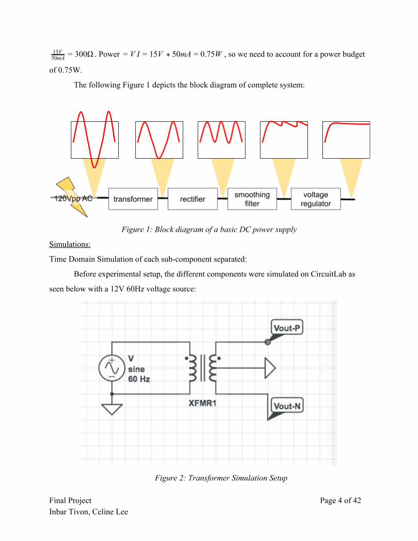
The following Figure 1 depicts the block diagram of complete system:
Figure 1: Block diagram of a basic DC power supply
Simulations:
Time Domain Simulation of each sub-component separated:
Before experimental setup, the different components were simulated on CircuitLab as
seen below with a 12V 60Hz voltage source:
Figure 2: Transformer Simulation Setup
Final Project Page 4 of 42 Inbar Tivon, Celine Lee

Figure 3: Transformer Simulation
Figure 3 plotted the time domain output of the wall voltage and nodes Vout-P and
Vout-N, as shown in Figure 2 above. The wall voltage peaked at 120VRMS, Vout-P peaked at
positive 16.2V, or ~11.5VRMS, and Vout-N peaked at the opposite -16.2V. By grounding the
center tap, Vout-P and Vout-N became 180 out of phase.°
Figure 4: Rectifier Simulation Setup
Final Project Page 5 of 42 Inbar Tivon, Celine Lee

Figure 5: Rectifier Simulation
Figure 6: Smoothing filter Simulation Setup
Final Project Page 6 of 42 Inbar Tivon, Celine Lee
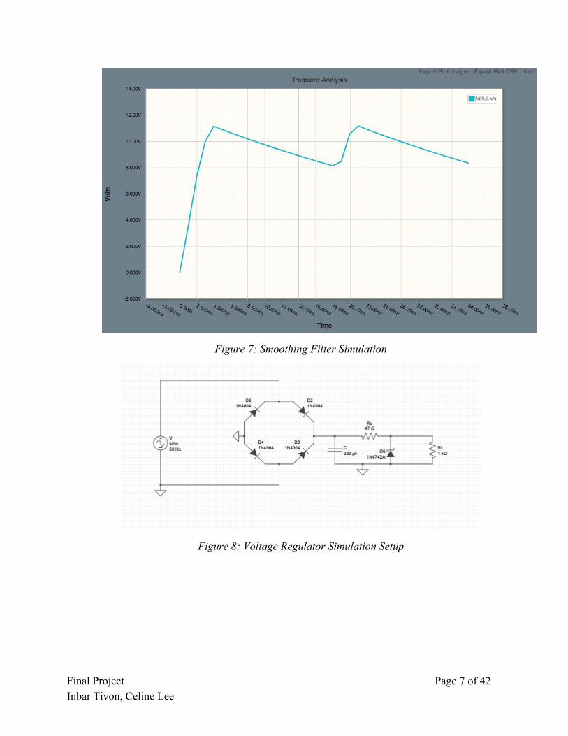
Figure 7: Smoothing Filter Simulation
Figure 8: Voltage Regulator Simulation Setup
Final Project Page 7 of 42 Inbar Tivon, Celine Lee

Figure 9: Voltage Regulator Simulation
Time Domain simulation of entire power supply:
Figure 10: Schematic of Entire Power Supply
Final Project Page 8 of 42 Inbar Tivon, Celine Lee

Figure 11: Simulation of Power Supply Showing Each Stage’s Positive Output
Figure 12: Simulation of power supply showing 15V open circuit voltage
Final Project Page 9 of 42 Inbar Tivon, Celine Lee
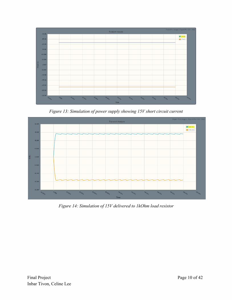
Figure 13: Simulation of power supply showing 15V short circuit current
Figure 14: Simulation of 15V delivered to 1kOhm load resistor
Final Project Page 10 of 42 Inbar Tivon, Celine Lee

Figure 15: Simulation showing 15V delivered to a load equal to equivalent resistance of other
subsystems (200 Ohm)
**We could not find the right zener diode in CircuitLab, so the ripples on the simulation are not
quite what came through on the oscilloscope.
Setup:
We used an oscilloscope to examine our power supply output. After plugging the
transformer in to the wall outlet, we used BNC-to-grabber cables to probe the power supply, and
examined the waveform on the oscilloscope. We used an oscilloscope rather than a multimeter
because we wanted to see how output changes over time. For example, we could use the
oscilloscope to see the output waveform fluctuate after the bridge rectifier. Then even with our
DC output, we could use the oscilloscope to examine the ripple voltage. The oscilloscope allows
us to look at the peak-to-peak voltage of our output response, otherwise known as Vr, our ripple
voltage. By dividing the ripple voltage by the average output, we can get the ripple fraction to
qualify how effective our smoothing filter and voltage regulators are. Each sub-component of the
power supply is verified by measuring the output on the oscilloscope. We expect the output to be
as specified in figure 1.
Final Project Page 11 of 42 Inbar Tivon, Celine Lee

Experimental Procedure:
All testing of the power supply was done by examining output on the oscilloscope. We
probed at the following locations on Figure 16:
Figure 16: Probing locations on the power supply
We probed at points A to examine output after the transformer, points B to examine rectified
output, and points C to examine our desired DC output. On the oscilloscope, we used the
measuring options to look at peak-to-peak voltage at each stage. For points A, we expect the
voltage to be a sine wave with magnitude 16V. At points B, we expect the outputs to be rectified
sine waves, with a voltage drop to have magnitude of about 14.15V. Each rectified “wave”
should either be all positive values, or all negative values. At points C, the output should be a
relatively steady DC voltage, with minimal ripple voltage.
Final Project Page 12 of 42 Inbar Tivon, Celine Lee

Experimental results:
At point A (after transformer):
Figure 17: Transformed waveform.
The peak-to-peak voltage is about 33.6V, which is appropriate for our ~16V amplitude wave
desired after the transformer.
At point B (after rectifier):
Figure 18: Rectified input
Final Project Page 13 of 42 Inbar Tivon, Celine Lee
We can see that the rectified input has a peak-to-peak voltage of 16.14V, slightly less than half
of the non-rectified input’s peak-to-peak.
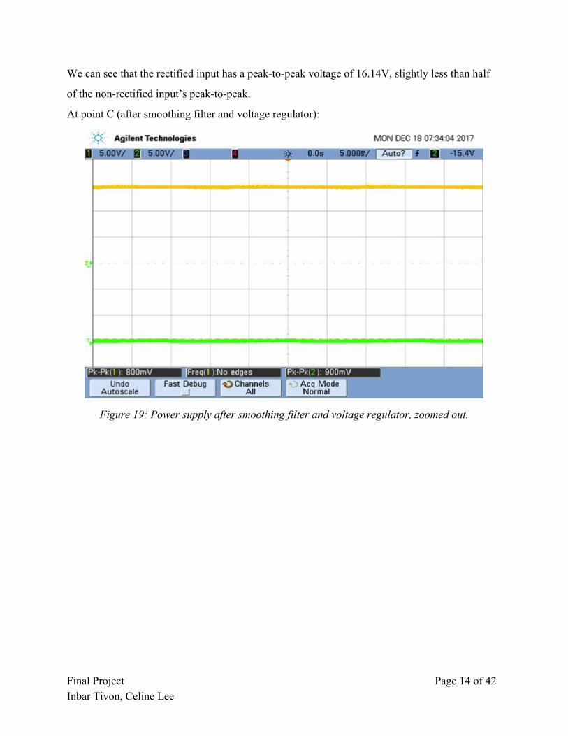
At point C (after smoothing filter and voltage regulator):
Figure 19: Power supply after smoothing filter and voltage regulator, zoomed out.
Final Project Page 14 of 42 Inbar Tivon, Celine Lee
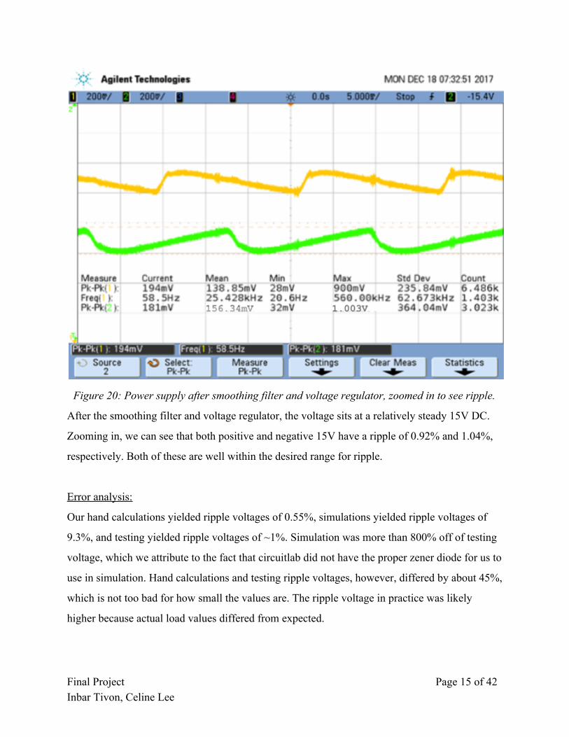
Figure 20: Power supply after smoothing filter and voltage regulator, zoomed in to see ripple.
After the smoothing filter and voltage regulator, the voltage sits at a relatively steady 15V DC.
Zooming in, we can see that both positive and negative 15V have a ripple of 0.92% and 1.04%,
respectively. Both of these are well within the desired range for ripple.
Error analysis:
Our hand calculations yielded ripple voltages of 0.55%, simulations yielded ripple voltages of
9.3%, and testing yielded ripple voltages of ~1%. Simulation was more than 800% off of testing
voltage, which we attribute to the fact that circuitlab did not have the proper zener diode for us to
use in simulation. Hand calculations and testing ripple voltages, however, differed by about 45%,
which is not too bad for how small the values are. The ripple voltage in practice was likely
higher because actual load values differed from expected.
Final Project Page 15 of 42 Inbar Tivon, Celine Lee

Section Conclusion:
Our resulting power supply output was a reliably steady constant voltage. The higher the load
resistance value, the steadier the voltage, which was something we needed to account for when
making the supply. At first, we found capacitor and resistor values that worked perfectly with a
load resistance of 2 , but as soon as we reduced load to 1 or 200 , the ripple became tooΩk Ωk Ω
large. Once we accounted for the lowest reasonable load resistance, we got our final working
power supply. The only other change we made while building the power supply was our zener
diode, which we did not realize until after the first round of testing, was a 5V zener. When it
began to get much too toasty, we replaced it with the 15V zener given to us.
Part 2: Filter Component
Pre-lab hand calculations:
We used the multiple feedback passband filter as our model for both our treble and bass filters.
Figure 21: Multiple Feedback Passband Filter Model
Transfer function hand calculations:
Let A = voltage across R1B; B = V n; s = j ω
R1A
A−V i + 1/jωC1
A−V OUT + AR1B
+ A−B1/jωC2
= 0
B−A1/jωC2
+ R2
B−V OUT = 0
; V p = V n B = 0
Final Project Page 16 of 42 Inbar Tivon, Celine Lee
( ωC ωC ) (− ωC )A 1R1A
+ j 1 + 1R1B
+ j 2 + B j 2 = V iR1A
+ V OUT1/jωC1
BjωC jωC )( )A = ( 2 + V iR1A
+ V OUT 1R R1A 1B
R +R +R R jω(C +C )1B 1A 1A 1B 1 2
C ( )( ) C ( )(sC V )− s 2R R1A 1B
R +R +R R s(C +C )1B 1A 1A 1B 1 2
V iR1A
= R2
V OUT + s 2R R1A 1B
R +R +R R s(C +C )1B 1A 1A 1B 1 2 1 OUT
)( )V iV OUT
= ( 1R2
+ sC sC R R2 1 1A 1BR +R +R R s(C +C )1B 1A 1A 1B 1 2 −sC R2 1B
R +R +R R s(C +C )1B 1A 1A 1B 1 2
= R (−sC R )2 2 1B
R +R +R R s(C +C )+R (s C C R R )1B 1A 1A 1B 1 2 22
2 1 1A 1B
V i
V OUT = −s(R C R )2 2 1Bs (R C C R R )+s(R R (C +C ))+(R +R )2
2 2 1 1A 1B 1A 1B 1 2 1B 1A
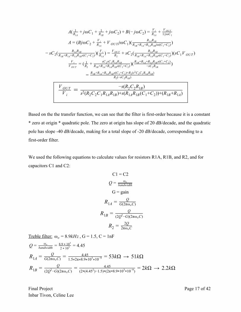
Based on the the transfer function, we can see that the filter is first-order because it is a constant
* zero at origin * quadratic pole. The zero at origin has slope of 20 dB/decade, and the quadratic
pole has slope -40 dB/decade, making for a total slope of -20 dB/decade, corresponding to a
first-order filter.
We used the following equations to calculate values for resistors R1A, R1B, and R2, and for
capacitors C1 and C2:
C1 = C2
Q = ωobandwidth
G = gain
R1A = QG(2πω C)o
R1B = Q(2Q −G)(2πω C)2
o
R2 = 2Q2πω Co
Treble filter: , G = 1.5, C = 1nF.9kHzωo = 8
.45Q = ωobandwidth =
2 10* 38.9 10* 3
= 4
→ 3kΩR1A = QG(2πω C)o
= 4.451.5 2π 8.9 10 10* * *
3*
−9 = 5 1kΩ 5
→ kΩR1B = Q(2Q −G)(2πω C)2
o= 4.45
(2 (4.45 )−1.5) (2π 8.9 10 10 )* 2 * * * 3* −9 = 2 .2kΩ 2
Final Project Page 17 of 42 Inbar Tivon, Celine Lee

→ 59kΩR2 = 2Q2πω Co
= 2 4.45*2π 8.9 10 10* *
3*
−9 = 1 60kΩ 1
Bass filter: , G = 1.5*, C = 0.22 F**50Hzωo = 2 μ
.25Q = ωobandwidth = 200
250 = 1
.8kΩR1A = QG(2πω C)o
= 1.251.5 2π 250 0.22 10* * * *
−6 = 1
.3kΩR1B = Q(2Q −G)(2πω C)2
o= 1.25
(2 (1.25 )−1.5) (2π 250 0.22 10 )* 2 * * * * −6 = 3
.2kΩR2 = 2Q2πω Co
= 2 1.25*2π 250 0.22 10* * *
−6 = 8
We chose a gain of 1.5 because we wanted any minor static produced during the filtering process
to be masked by the increase in volume. Also, since a bandpass filter tends to push the gain
down, we wanted to artificially raise the gain to “make up” for the loss. The capacitance values
were chosen after some hand calculation trial-and-error because it yielded the best resistor values
available in Detkin lab.
The expected input of these filters are waveforms of various frequencies, and the output should
be the waveforms either attenuated, if it is outside the bandwidth, or with the appropriate gain, if
within the bandwidth. The output load is the speaker.Ω8
We require a DC supply of 15V to rail our op-amps. We also need a maximum of about 25mA
current to run each op-amp. Power is current times voltage, so we need to budget 15V * 50mA =
0.75W of power.
Pre-lab simulation:
To create the filters, we use a TL071 op-amp, the specified resistors, and two audio jacks:
one for input, and one for output. The 15-volt DC voltage delivered to the Op-Amp rails are
provided by our power supply, detailed in section 1 of the lab report.
Final Project Page 18 of 42 Inbar Tivon, Celine Lee

Figure 22: Schematic for Treble Filter
Figure 23: Treble Bode Plot with Center Frequency Label
Final Project Page 19 of 42 Inbar Tivon, Celine Lee

Figure 24: Treble Bode plot with low cut-off labeled
Figure 25: Treble Bode with high cut-off labeled
Final Project Page 20 of 42 Inbar Tivon, Celine Lee

Figure 26: Treble Bode plot for phase
Slope, and thus roll-off rate, of bode plot is -20dB/decade, so it is a first-order filter.
Figure 27: Schematic for Bass filter
Final Project Page 21 of 42 Inbar Tivon, Celine Lee

Figure 28: Bass Bode plot with center frequency labeled
Figure 29: Bass Bode plot with low cut-off labeled
Final Project Page 22 of 42 Inbar Tivon, Celine Lee

Figure 30:Bass Bode with high cut-off labeled
Figure 31: Treble Bode plot for phase
Slope, and thus roll-off rate, of bode plot is -20dB/decade, so it is a first-order filter.
Input/output impedance of each subcomponent shown:
The impedance of each resistor is simply its resistance in Ohms. The impedance of each
capacitor is 1/jwC Ohms.
Time domain simulation at center frequencies:
Final Project Page 23 of 42 Inbar Tivon, Celine Lee

Figure 32: Time Domain Simulation of input/output Treble at center frequency (8.8kHz)
Figure 33: Time Domain Simulation of input/output Bass at center frequency (237Hz)
Final Project Page 24 of 42 Inbar Tivon, Celine Lee

Time domain simulations at cutoff frequencies:
Figure 34: Time Domain Simulation of input/output Treble at low corner frequency (7.58kHz)
Figure 35: Time Domain Simulation of input/output Treble at high corner frequency 9.89kHz)
Final Project Page 25 of 42 Inbar Tivon, Celine Lee
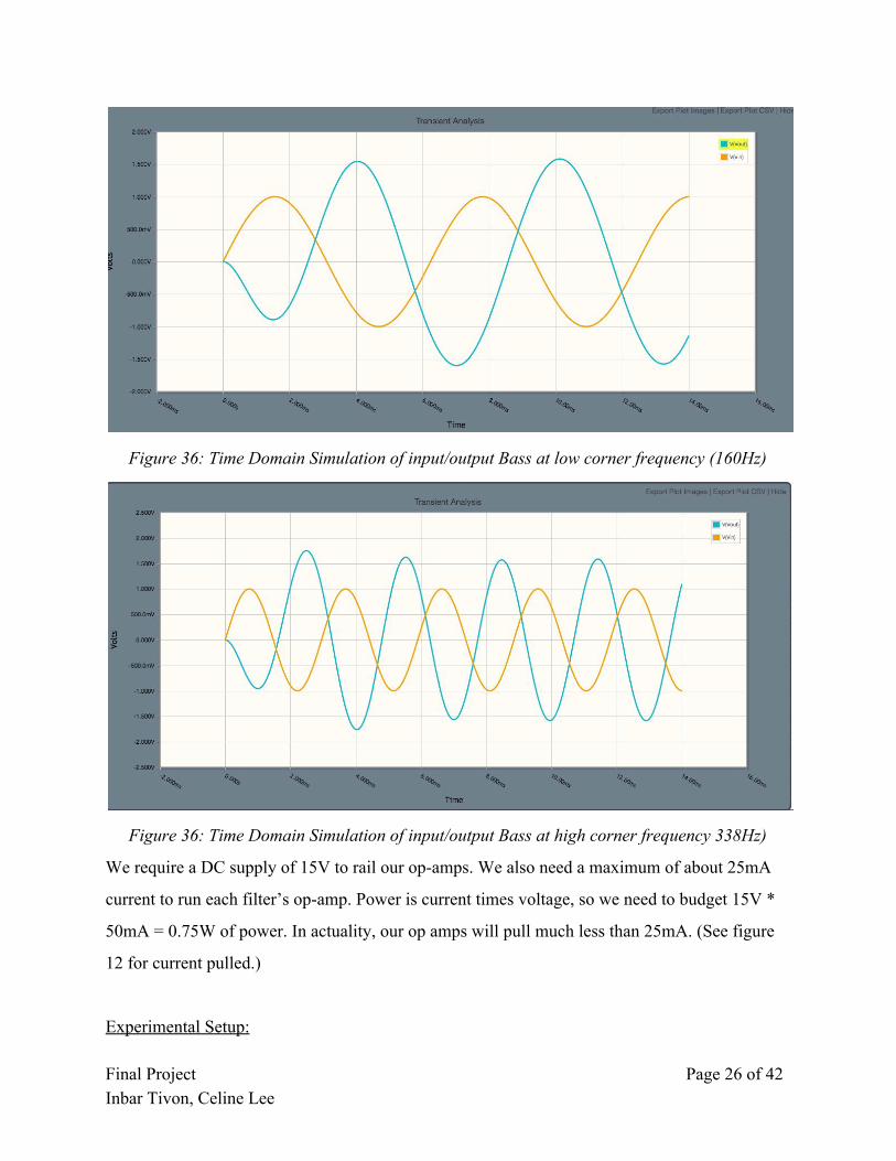
Figure 36: Time Domain Simulation of input/output Bass at low corner frequency (160Hz)
Figure 36: Time Domain Simulation of input/output Bass at high corner frequency 338Hz)
We require a DC supply of 15V to rail our op-amps. We also need a maximum of about 25mA
current to run each filter’s op-amp. Power is current times voltage, so we need to budget 15V *
50mA = 0.75W of power. In actuality, our op amps will pull much less than 25mA. (See figure
12 for current pulled.)
Experimental Setup:
Final Project Page 26 of 42 Inbar Tivon, Celine Lee

We use an oscilloscope and a waveform generator to test our filter. On the waveform, we
set a sine wave at 300mV, then examine the output on the oscilloscope at various set frequencies.
We want to use an oscilloscope rather than a multimeter because it allows us to observe
frequency response, which would be too difficult to gauge on a multimeter. Observe the
schematic below for how we connected our circuit to the waveform generator and oscilloscope:
To test the treble filter, we set the frequency to 6kHz (below the cutoff), 7.9kHz (lower
cutoff), 8.9kHz (middle of range), 9.9kHz (upper cutoff), and 11kHz (above the cutoff). To test
the bass filter, we set the frequency to 100Hz (below the cutoff), 150Hz (lower cutoff), 250Hz
(middle of range), 350Hz (upper cutoff), and 400Hz (above the cutoff). At or between the
cutoffs, we should get a voltage within max voltage and max voltage divided by . Below and√2
above the cutoffs, we should get an output less than max voltage divided by .√2
Experimental Procedure
In testing the filter, we generated a waveform, twiddled the frequency until we hit a max
amplitude, and declared that frequency the center frequency. Then to find the corner frequencies,
we took the max amplitude and divided by . Then again, we twiddled the frequency again√2
until we got two different frequencies, one less than and one greater than the center frequency,
that gave gain equal to the max amplitude divided by .√2
From the power supply, we require a DC supply of 15V to rail our op-amps. We also
need a maximum of 50mA current to run the two op-amps. Power is current times voltage, so we
need to budget 15V * 50mA = 0.75W of power.
Final Project Page 27 of 42 Inbar Tivon, Celine Lee

Final Project Page 28 of 42 Inbar Tivon, Celine Lee

Experimental results
Treble:
Figure 37: Time domain output at Treble center frequency 8.89kHz
Final Project Page 29 of 42 Inbar Tivon, Celine Lee

Figure 38: Time domain output at Treble high cutoff frequency 10.99kHz
Final Project Page 30 of 42 Inbar Tivon, Celine Lee

Figure 39: Time domain output at Treble low cutoff frequency 7.91kHz
Bass:
Figure 40: Time domain output at Bass center frequency 249 Hz
Final Project Page 31 of 42 Inbar Tivon, Celine Lee

Figure 41: Time domain output at Bass low cutoff frequency 149.7Hz
Figure 42: Time domain output at Bass high cutoff frequency 350Hz
Final Project Page 32 of 42 Inbar Tivon, Celine Lee

Notice that the cutoff frequencies have peak-to-peak value of approximately the center frequency
peak-to-peak value divided by .√2
.08VV center = 2
.4VV cutof f = √22.08 = 1
The cutoff frequencies of 7.91kHz and 10.99kHz have the cutoff peak-to-peak voltage. Figures
37 through 42 show the difference in magnitude for various frequencies.
Figure 40: Phase difference between Treble input and output waveforms.
Final Project Page 33 of 42 Inbar Tivon, Celine Lee

Figure 40: Phase difference between Bass input and output waveforms.
Figure 41a: Bode plot of magnitude on oscilloscope: Treble.
Final Project Page 34 of 42 Inbar Tivon, Celine Lee

Figure 41b: Bode plot of magnitude on oscilloscope: Bass.
Error analysis
Table 1: Treble Filter Error Analysis
Hand Calc Simulation Measurement % diff btw hand and meas.
% diff btw sim. and meas.
Low cut off 7.9kHz 7.58kHz 7.91kHz 0.13% 4.17%
High cut off 9.9kHz 9.89kHz 10.99kHz 9.92% 10.01%
Center freq 8.9kHz 8.8kHz 8.89kHz 0.11% 1.01%
Bandwidth 2kHz 2.31kHz 3.08kHz 35.06% 25%
Q 4.45 3.81 2.88 54.51% 32.29%
The largest error was the percent difference in bandwidth of the Treble filter which
affected the Quality factor. Since our filter was first-order, the slightest change in resistor or
capacitor values had a great effect on the bandpass range. There was also an unaccounted-for
resistance of the audio jack block that may have altered the bandpass. Although the low cutoff
was spot-on, and the high cutoff is only 1kHz off, which is not too bad since treble takes in the
Final Project Page 35 of 42 Inbar Tivon, Celine Lee

higher-frequency audio signals anyway, this practically small deviation resulted in a large
percent difference.
Table 2: Bass Filter Error Analysis
Hand Calc Simulation Measurement % diff btw hand and meas.
% diff btw sim. and meas.
Low cut off 150Hz 160.3Hz 149.7Hz 0.20% 7.08%
High cut off 350Hz 338.8Hz 350Hz 0% 3.20%
Center freq 250Hz 237.1Hz 249Hz 0.40% 4.78%
Bandwidth 200Hz 178.5Hz 200.3Hz 0.15% 10.88%
Q 1.25 1.33 1.24Hz 0.81% 7.26%
As for the Bass filter, the actual measured values were a lot closer to expected compared
to the simulated values, which caused the 10.88% difference between them. This can be
attributed to element natural variance.
Section conclusion
Though percent difference between simulation and measured were fairly significant, our
resulting filters are reliable because they do filter the proper general range of frequencies.
Especially for bass, which was more selective, our filter exceeded expectations. For treble, the
lower cutoff frequency was spot-on, which is excellent. The higher cutoff frequency was 1kHz
higher than expected, which is unfortunate, but at least it is the higher cutoff for a range that
generally encompasses high frequencies anyway. While designing the filters, we actually started
with a cascading low-pass, high-pass filter, but since we were using first-order filters, the
resulting bandpass was much too wide. As a result, we instead switched to an infinite gain
multiple feedback filter, which used just one op-amp, which fixed the issue of bandpass
widening. Ultimately, we succeeded in our goal of designing a power supply, treble filter, and
bass filter.
Part 3: Final Integration
Final Project Page 36 of 42 Inbar Tivon, Celine Lee

Hand calculations
Our power supply can deliver up to We require a DC supply of 15V to rail our op-amps.
We also need about 25mA current per op-amp. Power is current times voltage, so for two
op-amps, we need to budget 15V * 50mA = 0.75W of power. The power supply can deliver up to
50mA, and each filter requires up to 25mA. 50mA = 25mA + 25mA. KCL is maintained.
Pre-lab simulation:
Figure 42: Simulation showing all components properly connected
Figure 43: Time Domain Simulation of Treble at center frequency (8.8kHz)
Final Project Page 37 of 42 Inbar Tivon, Celine Lee
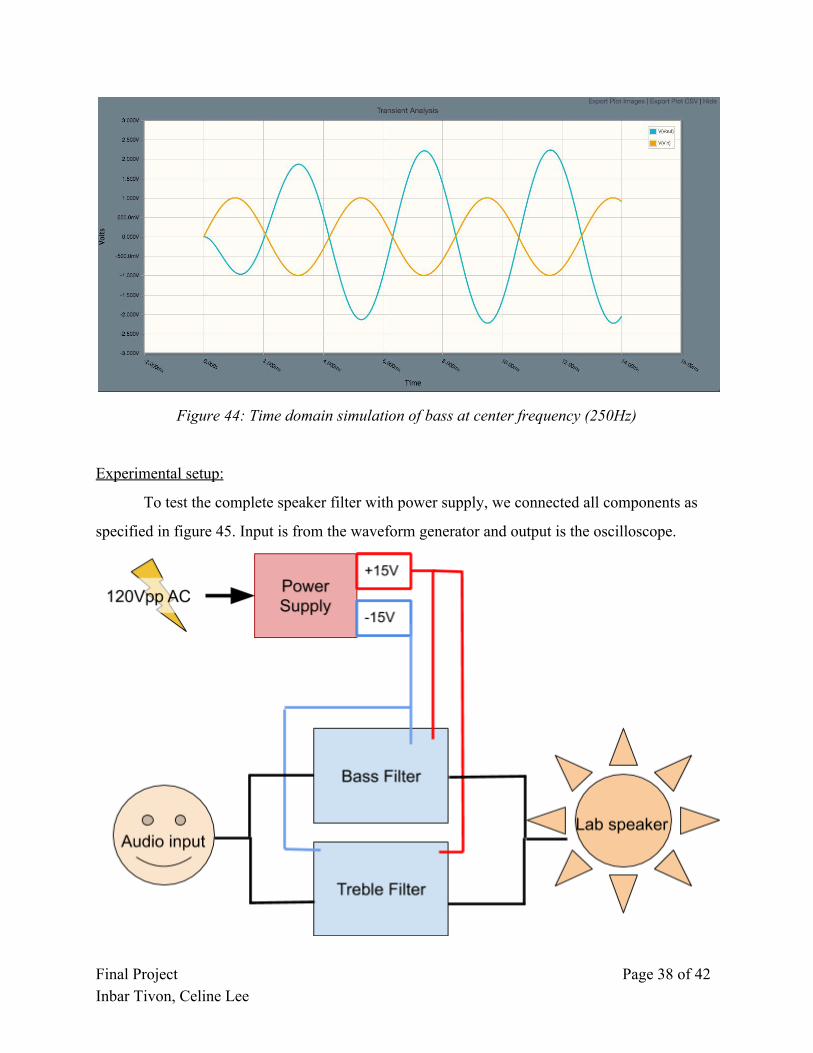
Figure 44: Time domain simulation of bass at center frequency (250Hz)
Experimental setup:
To test the complete speaker filter with power supply, we connected all components as
specified in figure 45. Input is from the waveform generator and output is the oscilloscope.
Final Project Page 38 of 42 Inbar Tivon, Celine Lee

Figure 45: Complete connected project, with power supply powering the op-amps.
We used the oscilloscope and waveform generator to test our filters. To test the treble
filter, we set the frequency on the waveform generator to 6kHz (below the cutoff), 7.9kHz (lower
cutoff), 8.9kHz (middle of range), 9.9kHz (upper cutoff), and 11kHz (above the cutoff). To test
the bass filter, we set the frequency to 100Hz (below the cutoff), 150Hz (lower cutoff), 250Hz
(middle of range), 350Hz (upper cutoff), and 400Hz (above the cutoff). At or between the
cutoffs, we should get a voltage within max voltage and max voltage divided by . Below and√2
above the cutoffs, we should get an output less than max voltage divided by .√2
We verified the output responses by using the measure function on the oscilloscope,
moving frequencies around until we achieved the desired voltage value.
Experimental Procedure
Before attaching the entire project together, we first tested the power supply under
various load resistances, to make sure that it would function properly, before connecting it to our
filters. Then we used the digital multimeter to ensure that amount of voltage being delivered by
the power supply to the filters is 15V. To test the filter itself, we used a triple output power
supply to power the rails, and examined output in response to various inputs on the oscilloscope
(as detailed in section 2).
Once we knew that both of these worked independently, we put the pieces together and
repeated the same testing procedure: make sure that the voltage being delivered from the power
supply to the rails were indeed +15V and -15V, and test filter response to various input
waveforms.
Experimental results
The final system composed of a power supply, two filters, and an extraneous LED
volume bar. See below:
Final Project Page 39 of 42 Inbar Tivon, Celine Lee

The power supply delivered 15V DC to the filter by scaling down and regulating voltage from a
wall outlet. The filters used the 15V DC to rail op-amps, which used in conjunction with our
particular arrangement of capacitors and resistors, created a bandpass filter. An audio jack
connects from an audio source to the filters, and another audio jack connects from the filter
output to the lab speakers.
Our simulated bandwidth for treble were [7.9kHz, 10.99kHz], and for bass were [150Hz,
350Hz]. Our measured bandwidths, however, were [7.9kHz, 9.9kHz] for treble and [160.3Hz,
338.8Hz] for bass. This is a 34% difference for treble, and 13% difference for bass.
Final Project Page 40 of 42 Inbar Tivon, Celine Lee

Figure 46: Complete build of final system
Error analysis
The 34% and 13% differences are fairly significant error percentages, and can be
attributed to a couple factors. For starters, we built first-order filters, so bandpass range was more
sensitive to minor differences in such values as resistance and capacitance. Another reason is that
we used an audio jack block to take input and give output, so there is unaccounted-for resistance
in that component that may affect the measured bandpass. Lastly, though the percent differences
are fairly large, we can point out that for bass, the measured bandpass is actually more selective
than the simulated, so this is not too bad of a difference. For the treble, the low cutoff is spot-on,
and the high cutoff is only 1kHz off, which is not too bad since treble takes in the
higher-frequency audio signals anyway.
Final conclusion:
Our final project worked beautifully. The filters successfully isolated treble and bass
frequencies from audio input and gave it a gain for the output. The power supply successfully
delivered 15V DC power with minute ripple voltage. Even the extra LED bar successfully
showed volume fluctuation.
The biggest difference between measurement and simulation for filters was in our treble
filter, at the high cutoff, with a 34% percent difference, as discussed in the error analysis of this
Final Project Page 41 of 42 Inbar Tivon, Celine Lee

section. The biggest difference overall, however, is ripple voltage between our measured and
simulated power supply, because CircuitLab did not have the zener diode we wanted. To account
for these differences, next time we could build a second-order filter to make the filter more
selective, thus narrowing the bandwidth.
From this project, we have learned that the best way to approach electrical engineering
projects is to start out with hand calculations and understanding simulations. Then, once we have
a clear picture of how to approach the task, start building the project component-by-component.
Since some relatively-unpredictable factors will change our output anyway, factor them in while
building and make modifications as necessary. Another lesson learned is that when playing with
potentially large amp values, always double-check calculations and simulations so that you do
not blow too many fuses or capacitors.
Final Project Page 42 of 42 Inbar Tivon, Celine Lee