influence of stencil design and...
TRANSCRIPT

W. Stęplewski, G. Kozioł, J. Borecki
73
1) Tele and Radio Research Institute, Centre of Advanced Technology, Ratuszowa 11, 03-450 Warszawa, Poland, e-mail: [email protected]* Praca prezentowana na XXXII International Conference of IMAPS - CPMP IEEE, Poland, Pułtusk, 21-24.09.2008
PL ISSN 0209-0058 MATERIAŁY ELEKTRONICZNE T. 37 - 2009 NR 1
INFLUENCE OF STENCIL DESIGN AND PARAMETERS OF PRINTING PROCESS ON LEAD-FREE PASTE
TRANSFER EFFICIENCY*
Wojciech Stęplewski1, Grażyna Kozioł1, Janusz Borecki1
Stencil design and stencil forming technique as well as parameters of solder paste printing process have an important influence on the volume and shape of solder paste deposited on the PCB pads and on the quality of solder joints. These factors become more crucial for fine pitch devices soldered in lead-free process. In the paper the results of experimental trials including selection of printing parameters, stencil materials and stencil forming technique as well as influence of different shapes of stencil apertures on transfer efficiency are discussed. The volume and shape of printed solder paste were measured and monitoring using microscopes and 3D inspection system.
Keywords: stencil, solder paste, 3D inspection, fine pitch device
1. INTRODUCTION
Screen printing of solder paste is a dominant process in surface mount techno-logy (SMT). Printing process of tin-lead solder paste is enough well-known and described in many sources. The conviction that implementation of lead-free soldering does not require essential modification in printing process prevailed until now. The recent results of research indicate that two factors such as use of lead-free soldering materials and fine pitch devices cause that printing process becomes one of the most crucial operation in lead-free SMT.

Influence of stencil design and parameters of printing process...
74
In the solder paste printing process, defects typically are caused by poor alignment between the substrate and stencil, incorrect material selection (substrate, paste type and stencil design) or variations in the amount of paste deposited [1].
The stencil thickness, stencil material and stencil forming technique as well as size and shape of stencil apertures are fundamental factors which influence on the quality of printing process and reliability of solder joints. Higher melting tempera-tures, worse wettability of lead-free solders, smaller dimensions of pads and smaller distance between components are the main reason that optimization of these factors plays the crucial role in assembly of fine pitch devices and creation of high quality solder joints.
Many industrial and research centers make the investigations on the selection of shapes and dimensions of apertures for lead-free soldering of fine pitch devices. However, the results of these investigations are often contradictory. Many of these elaborations should be examined in “real-life” large scale production. Usually chan-ging of shape and apertures dimensions is made in order to minimize of soldering defects such as formation of solder balls under component (the characteristic defect for R/C components), tombstoning, solder bridges, solder deficiencies, and excessive quantity of voids (BGA, CSP components) [2, 3].
2. BASIC PARAMETERS OF STENCIL DESIGN AND PRINTING PROCESS
Volume of solder paste transfered through stencil aperture is characterized by the geometrical parameters, such as aspect ratio, area ratio and transfer efficiency.
Aspect Ratio – The aspect ratio is the ratio of the aperture opening to the stencil thickness (eq. 1). For chemically etched stencils, this ratio should be greater than 1.5, for laser cut stencils it should be greater than 1.2 and for electroformed stencils which has the best solder paste release characteristics this ratio should be greater than 1.1. Anything less than these recommended ratios can cause the solder paste stick excessively to the walls of the aperture during release as the retaining force of the paste in the aperture will be stronger than the force pulling the paste out of the aperture [1, 4].
NADASPECT RATIOT
=
where: DNA – narrowest aperture dimension, T – stencil thickness.
Area Ratio – It is the relation between the surface of the aperture and the inside surface of the aperture walls (eq. 2). The major different with aspect ratio is that the area ratio is more suitable for shapes such as circles. Since solder paste has a certain
(1)

W. Stęplewski, G. Kozioł, J. Borecki
75
adhesion force, it will stick to the walls of the aperture and to the pad. Area ratio ≥0.66 is considered acceptable [1, 4-6].
P
W
AAREA RATIOA
=
where: AP – pad area, AW – wall area
Area ratio factor has the biggest single impact on transfer efficiency and repe-atability of the solder paste deposit.
Transfer Efficiency – The percentage of solder paste of the theoretical volume of the aperture that is transferred onto the pad (eq. 3, Fig. 1) [1, 4, 5, 7].
%D
A
VTransfer Efficiency (%) TE 100V
= = ×
where: VA – volume aperture (theoretical volume), VD – volume deposit (actual or predicted volume).
Fig. 1. Transfer of solder paste onto pad. Rys. 1. Przeniesienie pasty lutowniczej na pola lutownicze płytki drukowanej.
Transfer efficiency is the basic factor which determines correctness of solder paste printing. The principle of Release & Volumetric Repeatability is based on the relation between area ratio, transfer efficiency and standard deviation. The higher value of relative area ratio gives the higher the relative transfer efficiency and also the lower absolute standard deviation of the paste deposit (Fig. 2) [7, 8].
Printing parameters have a crucial influence on volume and shape of solder paste deposit. The optimal value of printing parameters determines the maximum of transfer efficiency and the best shape of deposited solder paste.
(2)
(3)

Influence of stencil design and parameters of printing process...
76
In the paper the results of selection of the printing parameters (print speed, squ-eegee pressure and separation speed), stencil materials and stencil forming technique as well as influence of different shape of stencil aperture on transfer efficiency are discussed.
In the investigation were used the following stencils: stainless steel (SST) and polyimide stencils made by laser, stainless steel stencils made by etching, and nickel stencils made by electroforming. The thickness of stencils was about: 100 µm – for steel and nickel stencils and 125 µm – for polyimide ones. Printing of solder paste was done on the screen-printing machine MPM AccuFlex.
The following printing parameters were used:1. Print speed (speed of squeegee moving) - 20, 50 and 70 mm/s;2. Squeegee pressure (expressed in kilos for the squeegee length of 0.3 m) - 3, 5
and 7 kg;3. Separation speed (the speed at which the board separates from the stencil) - 1,
5 and 7 mm/s.
3. QUALITY CONTROL OF PASTE DEPOSIT
Automatic three-dimensional control system was applied for assessment of solder paste deposit quality.
The machine VisionMaster AP212 makes possibilities of quantitative and qu-alitative assessment of solder paste deposits. It enables quick statistic analysis of received results and verification of printing parameters for different stencil designs. Additionally, the microscopic control and X-ray inspection were carried out. Based
Fig. 2. The area ratio factor impact on transfer efficiency of the solder paste through the stencil apertures.Rys. 2. Zależność efektywności uwalniania pasty oraz odchylenia standardowego od współ-czynnika area ratio.

W. Stęplewski, G. Kozioł, J. Borecki
77
on the results obtained using these control methods we try to describe the influence of stencil aperture shapes and printing parameters on transfer efficiency of solder paste.
Stencil apertures clogging (Fig. 3) was also observed. This factor can cause the inaccuracy of solder paste printing and can be a source of failures after soldering process.
Fig. 3. Stencil apertures clogging.Rys. 3. Pozostawanie pasty w oknach szablonu.
4. INFLUENCE OF STENCIL MATERIALS AND STENCIL FORMING TECHNIQUE
The experimental trials were performed in fractional mode. In summary, nine combinations (experimental trials) with all variables were done. For each combination the five repetitions were carried out for four types of stencils. The stencils apertures have the same shape and size as the pad for the components. In all tests a lead free solder paste based on the SAC 305 alloy, powder type 4 (20-38 µm grains) and flux ROL1 was used.
During the tests it was noticed that the stencils made with nickel electroformed technology gave the best results in fine pitch devices assembly. Laser cut stainless steel stencil had comparable utilize properties. For these two types of stencils the best transfer efficiency was obtained (Figs. 4-6). Presented average results were

Influence of stencil design and parameters of printing process...
78
obtained with printing parameters: print speed – 20 mm/s, squeegee pressure – 5 kg and separation speed – 3 mm/s.
Fig. 4. The average transfer efficiency, 0201 component.Rys. 4. Średnia efektywność trnasferu pasty, podzespół 0201.
Fig. 5. The average transfer efficiency, CSP132T.5 component.Rys. 5. Średnia efektywność trnasferu pasty, podzespół CSP132T.5.
Fig. 6 The average transfer efficiency, BGA46T.75 component.Rys. 5. Średnia efektywność trnasferu pasty, podzespół BGA46T.75.

W. Stęplewski, G. Kozioł, J. Borecki
79
The worst results were obtained in case of polyimide stencil. But this stencil has larger thickness. By this way it has the lowest value of area ratio. This causes more possibility to stencil apertures clogging.
5. SELECTION OF PRINTING PARAMETERS
The printing parameters should guarantee the proper filling of apertures during movement of squeegee and easy separation of solder paste from stencil apertures walls. During experimental trials it was observed that the low value of squeegee pressure (3 kg) causes remaining of thin film of solder paste on top surface of stencil. In case of big apertures it can cause too large volume of solder paste deposit on pad. But in case of small apertures (for fine pitch devices) it is possible that significant part of solder paste volume remains in stencil aperture. In effect the insufficient volume of solder paste is deposited on the pad (Fig. 7). The high value of squeegee pressure (7 kg) and the high speed of squeegee movement (70 mm/s) cause the scooping of solder paste from stencil aperture and in effect irregular thickness of solder paste deposits (Fig. 8).
Fig. 7. The deficiency of solder paste on one pad.Rys. 7. Deficyt pasty na jednym z pól lutow-niczych.
Fig. 8. The irregular deposition of solder paste on pads.Rys. 8. Nierównomierne rozmieszczenie pa-sty na polach lutowniczych
As the result of investigations the values of printing process parameters were chosen: the speed of squeegee 50 mm/s, the pressure of squeegee 5 kg, the speed of separation 1 mm/s.
6. DESIGN OF APERTURES
In the first part of investigations the stencil apertures which correspond with shape and size of PCB’s pads were designed for the fine pitch devices like 0201,

Influence of stencil design and parameters of printing process...
80
CSP132T.5C-DC145, BGA46T.75C-DC24 [9]. The area ratio for selected apertures (for fine pitch devices) is shown in Tab. 1.
Table. 1. The area ratio of stencil apertures for fine pitch devices chosen in first step of investigations [9].Tabela 1. Wartości parametru area ratio określonego równaniem (2) dla szablonów o grubości 100 µm i 125 µ.
Fine pitch deviceArea ratio of stencil apertures for
thickness of stencil
100 µm 125 µmR0201 0.750 0.591CSP132T.5 0.775 0.610BGA46T.75 0.750 0.591
At this point it should be noticed that the area ratio parameter with acceptable value (≥ 0.66) is achieved only for 100 µm stencil. Nowadays the designed PCBs have the electronic components with very diverse dimensions. Additionally, they are placed with greater density. By this reason stencils thickness and the shape of apertures must be individually elaborate for every kind of components including fine pitch electronic devices. The main part of presented investigations was focused on selection of optimal stencil apertures shape which allows achieving the best transfer efficiency.
The influence of different stencil aperture shapes in 100 µm stainless steel stencil made by laser technique was investigated. On the base of the literature [5, 10-12] and own experiences the several variants of apertures shape were elaborated, which are shown in Figs. 9-13.
Fig. 9. The apertures for pads for components 0201 and BGA46T.75C-DC24 (variant A) and CSP132T.5C-DC145 (variant A1).Rys. 9. Okna szablonu dla pól lutowniczych pod podzespoły 0201, BGA46T.75C-DC24 (wariant A) oraz CSP132T.5C-DC145 (wariant A1).
W. Stęplewski, G. Kozioł, J. Borecki
81
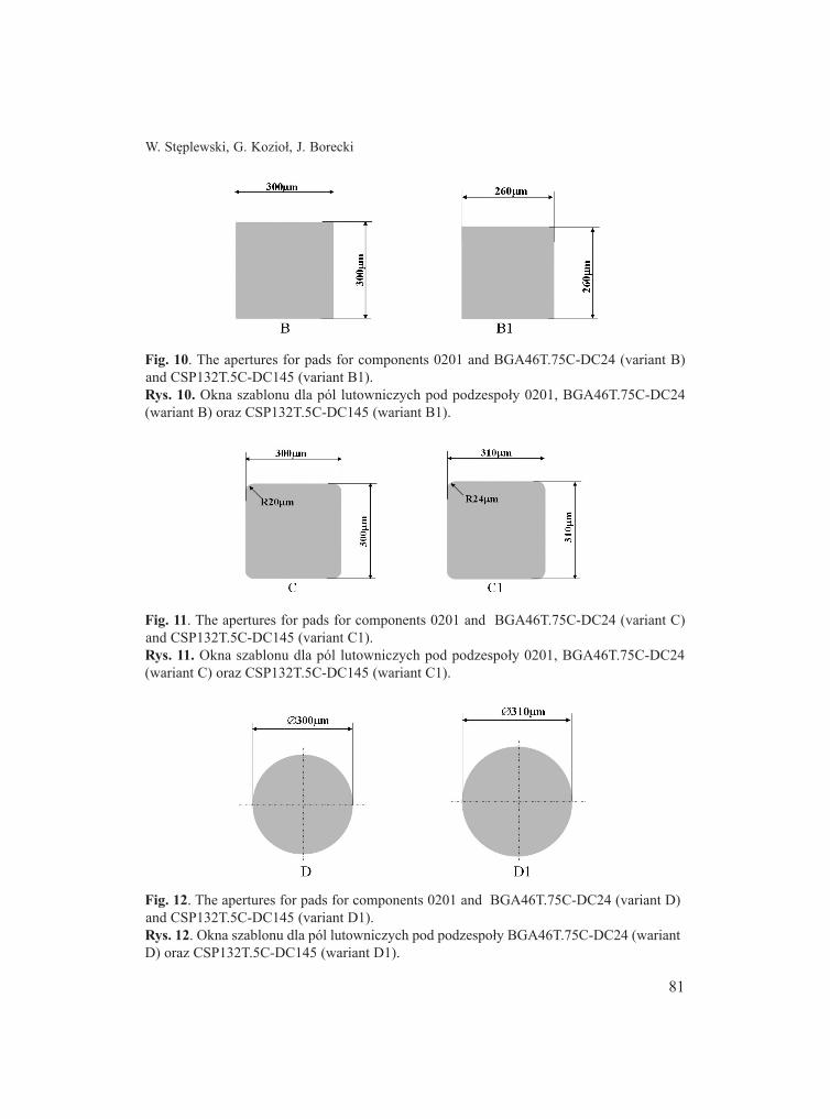
Fig. 10. The apertures for pads for components 0201 and BGA46T.75C-DC24 (variant B) and CSP132T.5C-DC145 (variant B1).Rys. 10. Okna szablonu dla pól lutowniczych pod podzespoły 0201, BGA46T.75C-DC24 (wariant B) oraz CSP132T.5C-DC145 (wariant B1).
Fig. 11. The apertures for pads for components 0201 and BGA46T.75C-DC24 (variant C) and CSP132T.5C-DC145 (variant C1).Rys. 11. Okna szablonu dla pól lutowniczych pod podzespoły 0201, BGA46T.75C-DC24 (wariant C) oraz CSP132T.5C-DC145 (wariant C1).
Fig. 12. The apertures for pads for components 0201 and BGA46T.75C-DC24 (variant D) and CSP132T.5C-DC145 (variant D1).Rys. 12. Okna szablonu dla pól lutowniczych pod podzespoły BGA46T.75C-DC24 (wariant D) oraz CSP132T.5C-DC145 (wariant D1).

Influence of stencil design and parameters of printing process...
82
The printing process was carried out with previous selected parameters (print speed 50 mm/s, squeegee pressure 5 kg, separation speed 1 mm/s). Lead-free solder paste based on the SAC 305 alloy, powder type 4 and flux ROL1 was used.
The results of printing process using different shapes of stencil apertures are shown in Figs. 14-16. In the diagrams the transfer efficiency is presented.
Fig. 13. The apertures for pads for components 0201 (variant E–„home”, F–“inverted home”, G–“D-shape”).Rys. 13. Okna szablonu dla pól lutowniczych pod podzespoły 0201 (wariant E – „home”, F – “inverted home”, G – “D-shape”).
Fig. 14. The average solder paste transfer efficiency, component 0201. Rys. 14. Średnia efektywność transferu pasty, podzespół 0201.

W. Stęplewski, G. Kozioł, J. Borecki
83
The best results are obtained in case of apertures with rounded corners (variant A, A1- Fig. 9; and variant C, C1 – Fig. 11). Transfer efficiency is distinctly better than in the case of other shapes. The worst results of solder paste printing process were obtained for apertures called as „home”, „inverted home” and „D - shape” (Fig. 13). For these shapes very strong adhesion of solder paste to aperture walls was observed. It was caused by the wedging of solder paste grains in sharp corners of the apertures. It can allow concluding that the use of apertures with sharp corners (≤ 90 °) is unfavourable in screen printing process for fine pitch devices.
The visual microscopic observations also show the very good quality of solder paste deposits with use square apertures with rounded corners. Paste mound deposits (for aperture shapes signed by A, A1, C, C1) had smooth walls and planar surface on the top. It confirms that the best results of screen printing process for fine pitch
Fig. 15. The average solder paste transfer efficiency, component CSP132T.5. Rys. 15. Średnia efektywność transferu pasty, podzespół CSP132T.5.
Fig. 16. The average solder paste transfer efficiency, component BGA46T.75.Rys. 16. Średnia efektywność transferu pasty, podzespół BGA46T.75.

Influence of stencil design and parameters of printing process...
84
devices can be achieved in case of stencil apertures designed with rounded corners. It thus arise from that the radius of the rounding of the aperture corner is higher than the radius of solder paste grains.
Oblong apertures are the particular case of apertures with rounded corners. This shape of aperture is recommended in screen printing process for multi-leads integrated circuits.
7. CONCLUSIONS
For lead-free assembly of fine pitch devices the formation of acceptable and repeatable solder paste deposits first of all depends on two group of factors. First group includes stencil material, stencil forming technique and stencil thickness. Fundamental factors of second group are size and shape of stencil apertures.
In our investigation the appreciation of correctness of solder paste printing based on experimental trials of different kinds of stencils and on analyses of solder paste transfer efficiency.
For the stencils with apertures having the same shape and size as the pads on the boards it was noticed that stencil made with nickel by electroforming technique gave the best results. Laser cut stainless steel stencil had comparable utilizable properties. Obtained an average transfer efficiency was as follows: 95% on pads for CSP, 79% on pads for 0201 and 84% on pads for BGA components for nickel stencil and 89% on pads for CSP, 82% on pads for 0201 and 80% on pads for BGA components for steel stencil.
The better transfer efficiency was stated for stainless steel stencil when apertures have rounded corners: nearly and over 100% on pads for 0201 and CSP and about 95% on pads for BGA components. The design of stencil aperture with rounded corners improves printing paste and should be used for small pads.
The result of trials indicates that the stencils made with nickel electroformed technology and apertures with rounded corners are needed for achieving optimal transfer of solder paste in fine pitch devices assembly.
REFERENCES
[1] Belmonte J., Boyes B., Johnson A.: SMT step by step. Step 4: Printing, SMT, April, (2005), 50-53
[2] Chrys Shea: Optimizing stencil design for lead-free SMT processing, Proceedings of the SMTA International Conference, Chicago, 2004

W. Stęplewski, G. Kozioł, J. Borecki
85
[3] WangM., Geiger D., Nakajima K., Shangguan D., Ho C.: Investigation 0201 printing issues and stencil design, Circuits Assembly, May (2003), 30-33
[4] Cookson Electronics Assembly Materials “Stencil Technology. TERMS, TIPS & TER-MINOLOGY”, Reference Bulletin, August 2003
[5] Cookson Standard Stencil Design, “Stencil Design Guidelines”, http://alpha.cooksone-lectronics.com/products/stencils/design.asp
[6] Bukat K., Hackiewicz H.: Lutowanie bezołowiowe, Wydaw. Btc, Warszawa 2007[7] Cookson Electronics Assembly Materials, Cookson Standards for Stencil Design. THE
POWER BEHIND THE PROCESS”, Reference Bulletin, August 2003[8] Shea Ch., Van Velthoven V., Tripp R.: Reducing variation in outsourced SMT manu-
facturing through the use of intelligent stencil systems, Cookson Electronics Assembly Material, 2003
[9] Stęplewski W., Kozioł G.: Stencil design for lead-free reflow process, Proceedings of ISSE (2007), 164-167
[10] Weldon T.: Optimised SMT stencil printing, Global SMT & Packing, April (2004), 24-28
[11] Shea Ch., Pandher R. S.: Stencil design for lead-free SMT assembly, Proceedings of the SMTA International Conference, Chicago, Illinois, 2004
[12] Arra M., Geiger D., Shangguan D., Sjoberg J.: Assembling fine pitch CSP packages, On Board Technology, September (2004), 38-41
WPŁYW PROJEKTOWANIA SZABLONU I PARAMETRÓW DRUKOWANIA NA EFEKTYWNOŚĆ TRANSFERU PASTY W LUTOWANIU BEZOŁOWIOWYM
Projektowanie i technika wykonania szablonu oraz parametry drukowania pasty lutowniczej mają istotny wpływ na objętość i kształt nadrukowanych „cegiełek” pasty lutowniczej i jakość połączenia lutowanego. Czynniki te stają się jeszcze bardziej krytyczne w przypadku podzespołów ultraminiaturowych w procesie lutowania bezołowiowego. W artykule przedstawiono rezultaty prób eksperymen-talnych obejmujących selekcję parametrów drukowania, różne materiały użyte na szablony i techniki ich wykonania oraz wpływ różnych kształtów okien w szablonie na efektywność transferu pasty. Pomiaru objętości i kształtu „cegiełek” drukowanej pasty dokonywano za pomocą mikroskopów (stereoskopowy, metalograficzny) oraz urządzenia do automatycznej trójwymiarowej inspekcji wizyjnej.
Słowa kluczowe: szablon, pasta lutownicza, inspekcja 3D, podzespół ultraminiatu-rowy