introduction to photonic integrated circuits
TRANSCRIPT

Microphotonic Devices Group
Introduction to Photonic Integrated Circuits
Min-Hsiung Shih(施閔雄)
Research Center for Applied Sciences (RCAS)&
Taiwan International Graduated Program (TIGP)Academia Sinica, Taiwan
May 9, 2008

Microphotonic Devices Group
Optical communication and photonic integrated circuits
Property of light
Elements for optical communication system1) Lasers and amplifiers2) Waveguides and fibers3) Modulators4) Multiplexer and Demultiplexer elements5) Photodectors
Photonic crystal waveguide and bending structures
Outlines

Microphotonic Devices Group
Speed Limitation of Electrical Communications

Microphotonic Devices Group
Optical Communication System
Typical DWDM (Dense Wavelength Division Multiplexing) system

Microphotonic Devices Group
Elements for Photonic Integrated Circuits
Microphotonic Devices Group
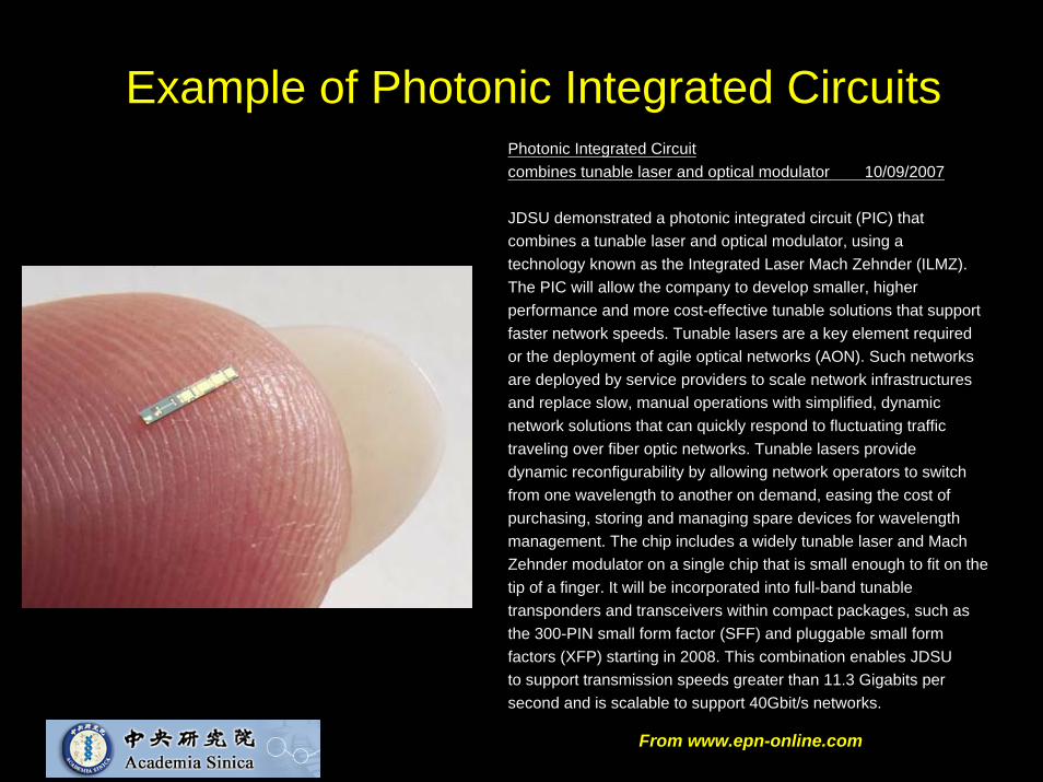
Example of Photonic Integrated CircuitsPhotonic Integrated Circuitcombines tunable laser and optical modulator 10/09/2007
JDSU demonstrated a photonic integrated circuit (PIC) thatcombines a tunable laser and optical modulator, using a technology known as the Integrated Laser Mach Zehnder (ILMZ).The PIC will allow the company to develop smaller, higher performance and more cost-effective tunable solutions that supportfaster network speeds. Tunable lasers are a key element requiredor the deployment of agile optical networks (AON). Such networksare deployed by service providers to scale network infrastructuresand replace slow, manual operations with simplified, dynamicnetwork solutions that can quickly respond to fluctuating traffic traveling over fiber optic networks. Tunable lasers providedynamic reconfigurability by allowing network operators to switchfrom one wavelength to another on demand, easing the cost ofpurchasing, storing and managing spare devices for wavelengthmanagement. The chip includes a widely tunable laser and MachZehnder modulator on a single chip that is small enough to fit on thetip of a finger. It will be incorporated into full-band tunabletransponders and transceivers within compact packages, such asthe 300-PIN small form factor (SFF) and pluggable small formfactors (XFP) starting in 2008. This combination enables JDSU to support transmission speeds greater than 11.3 Gigabits persecond and is scalable to support 40Gbit/s networks.
From www.epn-online.com
Microphotonic Devices Group
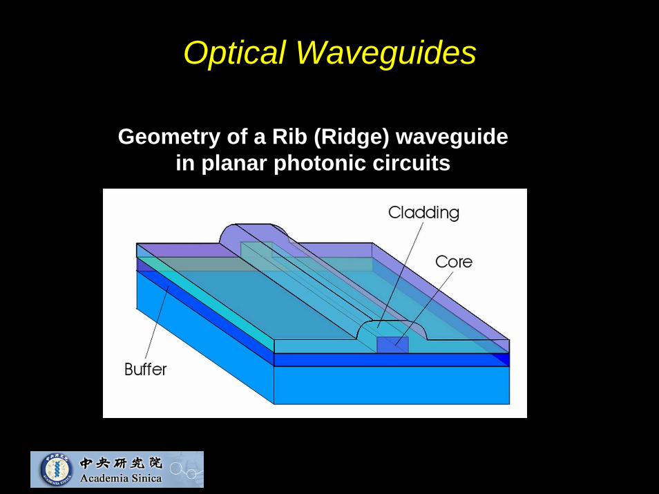
Optical Waveguides
Geometry of a Rib (Ridge) waveguide in planar photonic circuits

Microphotonic Devices Group
Types of Optical Waveguides
• SEM image of a dielectric rib (ridge) waveguide
• The calculated mode profile
n2
n1
n3

Microphotonic Devices Group
Optical Fiber
• High index core surround by lower index cladding
• The numerical aperture NA
0
2/122
sin
)(
nNA
nnNA claddingcore
=
−=
α

Microphotonic Devices Group
Semiconductor Lasers
Edge-emitting laser
VCSEL
DFB laser
Si Raman laser

Microphotonic Devices Group
Optical Amplifiers - EDFA• Erbium doped fiber
amplifier (EDFA)• Advantages
1. Cover wide wavelength range
2. Large total output power (> 1000 mW)
3. Large dynamic power range
• Disadvantages1. Not linear over the
working range2. Total power keep
constant for channels

Microphotonic Devices Group
Optical Amplifiers - SOA
• Semiconductor optical amplifier (SOA)
• Advantages1. For larger range of
wavelength
2. Easy to integrate to other elements
• Disadvantages1. Lower output power(5-
10 mW)
2. Crosstalk influences

Microphotonic Devices Group
Different Types of Optical Modulators
E-O Modulator Resonant Microdisk
Mach-ZehnderStructure
Size Large Compact
> 10 GHz
Vπ High Low Low
High
Larger
Speed > 10 GHz ~ 1 GHz
Cost Low Low

Microphotonic Devices Group
Demultiplexer Elements
Prism•Not used in DWDM system

Microphotonic Devices Group
Demultiplexer Elements
Diffraction Grating• Reflection light is not
homogeneous
• Not used in DWDM system
Microphotonic Devices Group
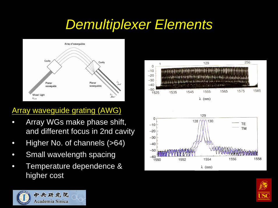
Demultiplexer Elements
Array waveguide grating (AWG)• Array WGs make phase shift,
and different focus in 2nd cavity• Higher No. of channels (>64)• Small wavelength spacing• Temperature dependence &
higher cost
λ (nm)
λ (nm)

Microphotonic Devices Group
Multiplexer Elements
• Optical couplers1. Simple, low cost
2. High insertion loss
3. Never be a DeMUX

Microphotonic Devices Group
Multiplexer Elements
Cascaded Mach- Zehnders
• Easy integrated
• Can be used for MUX/DeMUX

Microphotonic Devices Group
Photodectectors in Photonic Circuits
Transfer optical signals to electrical signals
The opposite way to lasers

Microphotonic Devices Group
Photodectectors in Photonic Circuits
Spectral response of different detector materials For fiber communication (~λ=1300-1550nm), InGaAs and Ge are prefer materials for photodetectors

Microphotonic Devices Group
End……

Microphotonic Devices Group
Photonic Crystal Devices for Photonic Integrated
Circuits
Min-Hsiung Shih(施閔雄)
Research Center for Applied Sciences (RCAS)&
Taiwan International Graduated Program (TIGP)Academia Sinica, Taiwan
May 16, 2008

Microphotonic Devices Group
Elements for Photonic Integrated Circuits

Microphotonic Devices Group
Building Blocks for Photonic Integrated Circuits with 2D Photonic Crystals
Laser / Light Source Waveguide / Bend Modulator
Photodetector
λ1, λ2, λ3 …
λ4, λ5, λ6 …

Microphotonic Devices Group
Photonic Crystal Defect Laser Cavity
• Micro-Disk Lasers
• Photonic Crystal D3 Membrane Cavity
• Continuous-Wave (CW) Operation Photonic Crystal Laser Cavity under

Microphotonic Devices Group
III-V Gain Materials for Semiconductor Lasers

Microphotonic Devices Group
Micro-Disk Laser Cavity
~ 5 μm
SEM image of a micro-disk laser from angle view4 InGaAsP
QWs enbeded
240 nm

Microphotonic Devices Group
Micro-Disk Laser CavityWhispering-gallery resonant modes
of a micro-disk
1st order mode 2nd order mode

Microphotonic Devices Group
Micro-Disk Laser Cavity
Lasing spectrum
1.40 1.45 1.50 1.55 1.60 1.65 1.70
0.0
20.0p
40.0p
60.0p
80.0p
100.0p
120.0p200712QW12 MD1_a6incident power = 6 mWduty cycle 1.5 % pulsed width 30 nsOSA res 1 nm
Mon
itor V
alue
(W)
Wavelength (μm)
1.35 1.40 1.45 1.50 1.55 1.60 1.650.0
1.0x10⁻¹¹
2.0x10⁻¹¹
3.0x10⁻¹¹
4.0x10⁻¹¹
5.0x10⁻¹¹
6.0x10⁻¹¹
7.0x10⁻¹¹
8.0x10⁻¹¹
Δλ=108nm
Mon
itor V
alue
(W)
Wavelength (μm)
PL from 200712QW 12incident power = 6 mW
λ=1555nm72.94 pW
PL spectrumGain peak ~ 1550 nm

Microphotonic Devices Group
0.0
0.1
0.2
0.3
0.4
0.5
0.6
0.7
In-Plane Propagation DirectionΓΚΜ
Nor
mal
ized
Fre
quen
cy (a
/λ0)
Γ
Membrane Photonic Crystal Defect Laser Cavity
Band Gap
Two dimensional triangular photonic crystal suspended membrane with r/a = 0.3, d/a=0.6 and dielectric constant ε=11.56
3D Band diagram of the photonic crystal membrane from finite-difference time-domain (FDTD) method
Microphotonic Devices Group
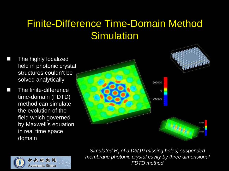
Finite-Difference Time-Domain Method Simulation
The highly localized field in photonic crystal structures couldn’t be solved analytically
The finite-difference time-domain (FDTD) method can simulate the evolution of the field which governed by Maxwell’s equation in real time space domain
Simulated Hz of a D3(19 missing holes) suspended membrane photonic crystal cavity by three dimensional
FDTD method

Microphotonic Devices Group
Quality Factor (Q) of CavityThe decay of energy in a cavity is expressed in term of the quality factor or Q.
Different notations1)1) Theoretical def. Theoretical def.
2)2) Experimental data in frequency domainExperimental data in frequency domain
3)3) Photon life time, Photon life time, ττpp
)()(2
noscillatioofcycleainlostenergyresonanceatcavitytheinstoredenergyQ π
=
2/1
0
ωωΔ
=Q
0ωτ Q
p =
Microphotonic Devices Group
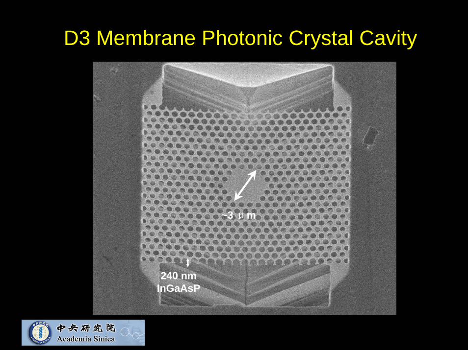
D3 Membrane Photonic Crystal Cavity
~3 μm
240 nm InGaAsP

Microphotonic Devices Group
Lasing Data from D3 Membrane Photonic Crystal Cavity
The lasing spectrum (red) of a suspended membrane D3 photonic crystal laser cavity.
The resonance peaks of the spectrum match well in the predicted normalized frequency which have higher quality (Q) factors and inside the high gain region.
0.32 0.33 0.34 0.35 0.36 0.37 0.38 0.39
0.01
0.1
1
0.31 0.32 0.33 0.34 0.35 0.36 0.37 0.38 0.39100
1000
10000
Res
onan
ce M
ode
Qua
lity
Fac
tor
Normalized Frequency (a/λ 0)
12/15/2002 offseted -0.025 in normalized frequency

Microphotonic Devices Group
Suspended Membrane and Sapphire-Bonded Structure
Sapphire substrate, n= 1.7
InGaAsP layer
Air-dielectric-air structure has better confinement for the localized fields
The structure only laseunder pulse width conditions
Air-dielectric-sapphire structure has less confinement for the localized fields
This structure can lase under continuous wave (CW) conditions
Thermal conductivityAir : 2.5x10⁻⁵ W/cm·K and Sapphire : 5x10⁻¹ W/cm·K

Microphotonic Devices Group
Quality Factor (Q) of Sapphire-Bonded Photonic Crystal Cavity
0.24 0.26 0.28 0.30 0.32 0.340
2,000
4,000
6,000
8,000
10,000
12,000
14,000
Qua
lity
Fact
or
a/λ
(a)
0.28 0.30 0.32 0.34 0.36 0.380
2,000
4,000
6,000
8,000
10,000
12,000
14,000
a/λ
(b)
D3 on Sapphire D3 on Air
0.24 0.26 0.28 0.30 0.32 0.340
2,000
4,000
6,000
8,000
10,000
12,000
14,000
a/λ0
D4 on Sapphire
0.24 0.26 0.28 0.30 0.32 0.340
2,000
4,000
6,000
8,000
10,000
12,000
14,000
a/λ0
D4 on Sapphire
(c)
D4
D3

Microphotonic Devices Group
Continuous Wave (CW) Operation of Sapphire-Bonded Photonic Crystal
Cavities
3.2 μm
SEM image of D4 sapphire-bonded cavity from angle view
1.57 1.58
-30
-20
-10
0
Out
put p
ower
(dB
)
Wavelength (μm)
0.0 0.5 1.0 1.5 2.0 2.50.0
0.2
0.4
0.6
0.8
1.0
Out
put P
ower
(a.u
.)
CW incident pumped power (mW)

Microphotonic Devices Group
Side-Mode Suppression Ratio (SMSR) of Sapphire-Bonded PhC Cavities
1.50 1.55 1.6010-12
10-11
10-10
10-9
10-8
(a)CW Condition
Inte
nsity
(a.u
.)
Wavelength (μm)
30 dB
1.50 1.55 1.6010-12
10-11
10-10 (b)
13 dB
Inte
nsity
(a.u
.)
Wavelength (μm)
Pulse Condition 8/800 ns
In fiber communication or CATV system, SMSR > 25 dB is considered a single mode light source.
Microphotonic Devices Group
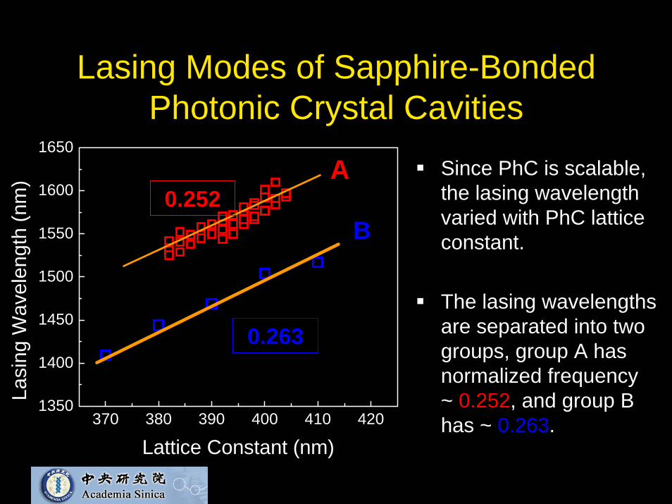
Lasing Modes of Sapphire-Bonded Photonic Crystal Cavities
Since PhC is scalable, the lasing wavelength varied with PhC lattice constant.
The lasing wavelengths are separated into two groups, group A has normalized frequency ~ 0.252, and group B has ~ 0.263.370 380 390 400 410 420
1350
1400
1450
1500
1550
1600
1650
B
Lasi
ng W
avel
engt
h (n
m)
Lattice Constant (nm)
A0.252
0.263

Microphotonic Devices Group
Comparison of Lasing Spectrum and 3D-FDTD Calculation
Mode B lasing spectrum (red curve)from a PhC laser under CW pumping condition.3D FDTD Calculated quality factor (Q) spectrum (orange) in normalized frequency axis.The shift between two spectra is about 1 %.
0.24 0.25 0.26 0.27 0.28
10-11
10-10
10-9
10-8
0.24 0.25 0.26 0.27 0.28102
103
104
Normalized Frequency (a/λ)
B
AIntensity (a.u.)
Qua
lity
Fact
or (Q
)
Microphotonic Devices Group
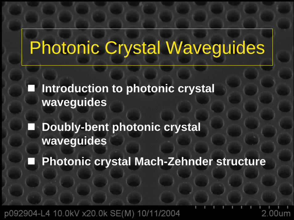
Photonic Crystal Waveguides
Introduction to photonic crystal waveguides
Doubly-bent photonic crystal waveguides
Photonic crystal Mach-Zehnder structure

Microphotonic Devices Group
Introduction to Photonic Crystal Waveguide
Band Gap
ΓK
0.0 0.2 0.4 0.6 0.8 1.00.0
0.1
0.2
0.3
0.4
Nor
mal
ized
Fre
quen
cy (a
/λ0)
In-Plane Propagation Constant β (x π/a)
0.0
0.1
0.2
0.3
0.4
0.5
0.6
0.7
In-Plane Propagation DirectionΓΚΜ
Nor
mal
ized
Fre
quen
cy (a
/λ0)
Γ

Microphotonic Devices Group
Types of Photonic Crystal Waveguides
Suspended Membrane
Oxide Substrate
Deeply Etched

Microphotonic Devices Group
Loss in Photonic Crystal Waveguides from FDTD
• The out-of-plane radiation loss of the waveguide is generally large for modes in the radiation light cone.
• Low loss transmission for suspended membrane and oxidized lower claddingstructures occurs at the vicinity of the Brillouinzone boundary.
projection of sapphire light cone
projection of air light cone
0.0 0.2 0.4 0.6 0.8 1.0
0.1
1
10
100
1000
10000
Thin Oxide Thick Oxide
Vert
ical
Rad
iatio
n Lo
ss (c
m-1)
In-plane Wave Vector β (π/a)
Deep Undercut Shallow Undercut
Deeply-Etched
3.0 μm
1.0 μm
From Wan Kuang, MPDG, USC

Microphotonic Devices Group
InGaAsP Membrane Photonic Crystal Waveguides
Suspended Membrane
InGaAsP
InP scarified layer
InP substrate

Microphotonic Devices Group
Fabrication of Photonic Crystal Membrane Waveguides
InP Substrate
InGaAsP 240 nm
SiNx layer 50 nm
PMMA 100 nm
E-Beam lithography
RIE CF4 Etching ECR etching
with CH4/H2/Ar HCl wet etching
at 0ºC
Remove all masks
lapping & cleaving

Microphotonic Devices Group
SEM Images of InGaAsP Membrane Photonic Crystal Waveguides
10 μm
10-15 periods

Microphotonic Devices Group
Transmission Through Straight Photonic Crystal Waveguides
Bandstructure and measured transmission of suspended membrane photonic crystal waveguide

Microphotonic Devices Group
Group Index of Propagated Mode in Photonic Crystal Waveguides
0.0 0.2 0.4 0.6 0.8 1.00.0
0.1
0.2
0.3
0.4
Nor
mal
ized
Fre
quen
cy (a
/λ0)
In-Plane Propagation Constant β (x π/a)
gg n
c=
∂∂
=βων
0.265 0.270 0.275 0.280 0.285 0.290 0.295 0.3000
10
20
30
40
50
60
1st band
2nd band
Gro
up in
dex
ng
Normalized Frequency
Group Indices of two guided bands

Microphotonic Devices Group
1480 1500 1520 1540 1560
4
6
8
10
Gro
up In
dex
Wavelength (nm)
r/a=0.30 r/a=0.33
0 5 10 15 20
Group Index
Spe
ctra
l Am
plitu
de
ng = 5.14
Comparison of the Predicted and Observed
Group Indices of Photonic Crystal Waveguides
Lng2
2λλ =Δ
Fabry-Perot oscillation period
Group indices of defect waveguide modes obtained from bandstructure
a= 420 nm, r/a = 0.315, Length = 292 μm

Microphotonic Devices Group
Fabry-Perot Oscillations from Doubly Bent Photonic Crystal Waveguides
LBend= 42.42 μm
31.92 μm
21.42 μm
Fabry-PerotRBend
RBend
Reflection from the two bends will lead to Fabry-Perot oscillations with a period that should be inversely proportional to LBend

Microphotonic Devices Group
1400 1450 1500 1550 16000.0
0.1
0.2
0.3
0.4
0.5
0.6
Tran
smis
sion
(a.u
.)
Wavelength (nm)
Theoretical Prediction of Transmission Through Photonic Crystal Waveguides by Finite Element
MethodCalculated Transmission
Straight waveguide
Bent waveguide
r/a = 0.3
74 nm

Microphotonic Devices Group
1460 1480 1500 1520 1540 1560 15800.0
0.2
0.4
0.6
0.8
1.0
Tran
smis
sion
(a.u
.)
Wavelength (nm)
Comparison of Transmission Measurement and Simulation
• Fabry-Perot oscillations were observed in measured transmission.
• The oscillation from the bent section can be identified by the period.
Measured result
r/a~0.31
Simulated result r/a=0.30

Microphotonic Devices Group
1480 1490 1500 1510 1520
Tran
smis
sion
( a.
u.)
Wavelength ( nm )
1500 1510 1520 1530 1540
Tran
smis
sion
( a.
u.)
Wavelength ( nm )
1500 1510 1520 1530 1540
Tran
smis
sion
( a.
u.)
Wavelength ( nm )
Reflectance Extracted from Measured Spectra
lengthLratiovalleytopeakK
KKR
LdB
::
1011 10
−−−
⎟⎟⎠
⎞⎜⎜⎝
⎛
+−
=⎟⎠⎞
⎜⎝⎛ α
Error-bars represent the range of αdBfrom 2 to 20 dB/mm.
LBend = 21.21 μm
1480 1490 1500 1510 1520
Tran
smis
sion
( a.
u.)
Wavelength ( nm )
LBend = 42.42 μm
1480 1500 1520 1540 1560
Tran
smis
sion
( a.
u.)
Wavelength ( nm )1500 1510 1520 1530 1540 1550
0.0
0.1
0.2
0.3
Wavelength ( nm )
Mea
sure
d R
efle
ctan
ce (a
.u.)

Microphotonic Devices Group
1520 1530 1540 15500.0
0.2
0.4
0.6
0.8
Wavelength ( nm )
Sim
ulat
ed R
efle
ctan
ce (a
.u.)
1520 1530 1540 15500.0
0.1
0.2
0.3
Wavelength ( nm )
Mea
sure
d R
efle
ctan
ce (a
.u.)
Simulated Reflectance
r/a > r/a ~ 0.3 r/a=0.30
Measured Reflectance
Comparison of Measured and Simulated Reflectance

Microphotonic Devices Group
Fabricate asymmetric Mach-Zehnder interferometers and characterize the transmission as a function of wavelength.
The Fourier transform of the transmission spectrum will contain information about the propagation coefficient of the photonic crystal waveguide mode.
The Basic Idea of Mach-ZehnderStructure

Microphotonic Devices Group
Photonic Crystal Mach-Zehnder
Structures in InP
InGaAsP/InP Membrane Structure

Microphotonic Devices Group
Mach-Zehnder Transmission Data
Wavelength (nm)
1550 1560 1570 1580 1590 1600 1610 1620
1550 1560 1570 1580 1590 1600 1610 1620
1550 1560 1570 1580 1590 1600 1610 1620
Inte
nsity
Inte
nsity
Inte
nsity
162015801560 1600
symmetric structure
path lengthdifference
75 μm
path lengthdifference121 μm
expect transmittedintensity to
contain oscillations that
go ascos(βΔL),
andβ= β(ng)

Microphotonic Devices Group
The Group Index of Photonic Crystal Waveguide
Three- Dimensional Finite Element Calculation

Microphotonic Devices Group
Fourier Transform of Transmission Spectra
Symmetric Mach-Zehnder
0 2000 4000 6000 8000 10000
No Dominant signals form the measured transmission

Microphotonic Devices Group
Mach-Zehnderwith Path Length Difference of 75 μm
Fourier Transform of Transmission Spectra
0 2000 4000 6000 8000 10000
502 μm Interference between two branches with a propagation index of 6.7

Microphotonic Devices Group
Fourier Transform of Transmission Spectra
Mach-Zehnderwith Path Length Difference of 121 μm
0 2000 4000 6000 8000 10000
637 μm
2230 μm
Interference between thetwo branches with a propagation index of 5.3
Fabry-Perot mode propagatingthrough the substrate

Microphotonic Devices Group
SummaryPhotonic crystal device, can be engineered by Photonic crystal device, can be engineered by changing the geometry, is a excellent candidate for changing the geometry, is a excellent candidate for dense photonic integrated circuits.dense photonic integrated circuits.
Photonic crystal defect laser cavities were obtained Photonic crystal defect laser cavities were obtained from from InGaAsPInGaAsP membrane.membrane.
Smallest continuousSmallest continuous--wave (CW) photonic crystal wave (CW) photonic crystal laser cavities was achieved on the sapphire laser cavities was achieved on the sapphire substrate.substrate.
Photonic crystal waveguides and its MachPhotonic crystal waveguides and its Mach--ZehnderZehnderstructure are demonstrated.structure are demonstrated.

Microphotonic Devices Group
Thank You
Microphotonic Devices Group
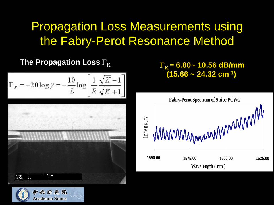
Propagation Loss Measurements using the Fabry-Perot Resonance Method
ΓK = 6.80~ 10.56 dB/mm (15.66 ~ 24.32 cm-1)
Fabry-Perot Spectrum of Stripe PCWG
1550.00 1575.00 1600.00 1625.00Wavelength ( nm )
Inte
nsi
ty
The Propagation Loss ΓK

Microphotonic Devices Group
Characterization Setup