investigation of silicon pin- detector for laser pulse
TRANSCRIPT
Department of Science and Technology Institutionen för teknik och naturvetenskap Linköpings Universitet Linköpings Universitet SE-601 74 Norrköping, Sweden 601 74 Norrköping
Examensarbete LITH-ITN-ED-EX--04/020--SE
Investigation of silicon pin-detector for laser pulse detection
Sam Chau
2004-05-19

LITH-ITN-ED-EX--04/020--SE
Investigation of silicon pin-detector for laser pulse detection
Examensarbete utfört i Elektronikdesign vid Linköpings Tekniska Högskola, Campus Norrköping
Sam Chau
Handledare: Mikael Lindgren, Berndt Samuelsson Examinator: Sayan Mukherjee
Norrköping 2004-05-19
Rapporttyp Report category Examensarbete B-uppsats C-uppsats D-uppsats _ ________________
Språk Language Svenska/Swedish Engelska/English _ ________________
Titel Undersökning av kisel pin-detektor för laser puls detektering Title Investigation of silicon pin-detector for laser pulse detection Författare Sam Chau Author
Sammanfattning Abstract This report has been written at SAAB Bofors Dynamics (SBD) AB in Gothenburg at the department of optronic systems. In military observation operations, a target to hit is chosen by illumination of a laser designator. From the targetpoint laser radiation is reflected on a detector that helps identify the target. The detector is a semiconductor PIN-type that has been investigated in a laboratory environment together with a specially designed laser source. The detector is a photodiode and using purchased components, circuits for both the photodiode and the laserdiode has been designed and fabricated. The bandwidth of the op-amp should be about 30 MHz, in the experiments a bandwidth of 42 MHz was used. Initially the feedback network, which consists of a 5.6 pF capacitor in parallel with a 1-kΩ resistor determined the bandwidth. To avoid the op-amp saturate under strong illuminated laser radiation the feedback network will use a 56-pF capacitor and a 100-Ω resistor respectively. The laser should be pulsed with 10-20 ns width, 10 Hz repetition frequency, about 800 nm wavelength and a maximum output power of 80 mW. To avoid electrical reflection signals at measurement equipment connections, the laser circuit includes a resistor of about 50 Ω, that together with the resistance in the laserdiode forms the right termination that eliminate the reflection signals. The wire-wound type of resistor shall be avoided in this application and instead a surface mounted type was beneficial with much lower inductance. The detector showed a linear behaviour up to 40-mW optical power. Further investigation was hindered by the breakdown of the laserdiodes. The function generator limits the tests to achieve 80 mW in light power. In different experiments the responsivity of the photodiode is different from the nominal value, however it would have required more time to investigate the causes.
ISBN _____________________________________________________ ISRN LITH-ITN-ED-EX--04/020--SE _________________________________________________________________ Serietitel och serienummer ISSN Title of series, numbering ___________________________________
Nyckelord Keyword Laserdiode, photodiode, silicon pin-detector, operational amplifier, responsivity, differential efficiency, bandwidth, feedback network
Datum Date 2004-05-19
URL för elektronisk version http://www.ep.liu.se/exjobb/itn/2004/ed/020/
Avdelning, Institution Division, Department Institutionen för teknik och naturvetenskap Department of Science and Technology
Abstract This report has been written at SAAB Bofors Dynamics (SBD) AB in Gothenburg at the department of optronic systems. In military observation operations, a target to hit is chosen by illumination of a laser designator. From the targetpoint laser radiation is reflected on a detector that helps identify the target. The detector is a semiconductor PIN-type that has been investigated in a laboratory environment together with a specially designed laser source. The detector is a photodiode and using purchased components, circuits for both the photodiode and the laserdiode has been designed and fabricated. The bandwidth of the op-amp should be about 30 MHz, in the experiments a bandwidth of 42 MHz was used. Initially the feedback network, which consists of a 5.6 pF capacitor in parallel with a 1-kΩ resistor determined the bandwidth. To avoid the op-amp saturate under strong illuminated laser radiation the feedback network will use a 56-pF capacitor and a 100-Ω resistor respectively. The laser should be pulsed with 10-20 ns width, 10 Hz repetition frequency, about 800 nm wavelength and a maximum output power of 80 mW. To avoid electrical reflection signals at measurement equipment connections, the laser circuit includes a resistor of about 50 Ω, that together with the resistance in the laserdiode forms the right termination that eliminate the reflection signals. The wire-wound type of resistor shall be avoided in this application and instead a surface mounted type was beneficial with much lower inductance. The detector showed a linear behaviour up to 40-mW optical power. Further investigation was hindered by the breakdown of the laserdiodes. The function generator limits the tests to achieve 80 mW in light power. In different experiments the responsivity of the photodiode is different from the nominal value, however it would have required more time to investigate the causes.

Preface It has been a pleasure to work at the company SAAB Bofors Dynamics AB in Gothenburg. I have been received with kind treatment among fellow workers and really appreciate the opportunity to write this thesis work at the company, and also make possible to finish my education. I honestly want to give sincere thanks to my supervisors Mikael Lindgren and Berndt Samuelsson for their help ing hands during the whole work and for their patience with me. Thank you guys, who let me join the floor ball game that brightens up one’s daily life in the work! Thanks to my examiner Sayan Mukherjee and the opponent Henrik Linderbäck who give me good advices to improve the report. Last but not least, thanks to my brother Jan with his wife Lian and also their lovely daughter Julia for letting me stay with them. Gothenburg, April 2004 Sam Chau

Table of contents
1 INTRODUCTION..........................................................................................................................................................1 1.1 BACKGROUND........................................................................................................................................................... 1 1.2 AIM............................................................................................................................................................................. 1 1.3 LIMITATIONS ............................................................................................................................................................. 2 1.4 METHOD..................................................................................................................................................................... 2
2 EQUIPMENT..................................................................................................................................................................3
3 THEORY..........................................................................................................................................................................4 3.1 OPERATIONAL AMPLIFIER....................................................................................................................................... 4
3.1.1 Simple op-amp structure................................................................................................................................5 3.1.2 Feedback (Describe with voltage amplifier)..............................................................................................6 3.1.3 Non-linear limits.............................................................................................................................................8 3.1.4 The full-power bandwidth.............................................................................................................................9
3.2 ENERGY BAND......................................................................................................................................................... 10 3.2.1 P-N Junction..................................................................................................................................................10 3.2.2 Photodetector................................................................................................................................................11 3.2.3 PIN-diode (PIN)............................................................................................................................................12 3.2.4 Photovoltaic and photoconductive modes................................................................................................12 3.2.5 Laser diode (LD)...........................................................................................................................................13
4 SYSTEM DESCRIPTION.........................................................................................................................................15 4.1 RECEIVER................................................................................................................................................................. 15 4.2 TRANSMITTER......................................................................................................................................................... 17
5 IMPLEMENTATION .................................................................................................................................................19 5.1 DETERMINE THE BANDWIDTH OF THE OP -AMP THEORETICALLY..................................................................... 19 5.2 INVESTIGATE THE BANDW IDTH OF THE OP -AMP PRACTICALLY....................................................................... 23 5.3 DESIGN OF THE LD-CIRCUIT ................................................................................................................................. 27 5.4 RESPONSIVITY......................................................................................................................................................... 30
6 RESULTS .......................................................................................................................................................................32 6.1 THE LD WITH 635-NM WAVELENGTH.................................................................................................................. 32 6.2 THE LD WITH 785-NM WAVELENGTH.................................................................................................................. 34
6.2.1 Saturation of the op-amp .............................................................................................................................35 6.2.2 Wire-wound type resistor ............................................................................................................................38 6.2.3 Metal film type resistor................................................................................................................................39 6.2.4 Widening of the pulse...................................................................................................................................41
7 DISCUSSION................................................................................................................................................................43
8 FUTURE WORK AND IMPROVEMENTS ........................................................................................................45
9 REFERENCES .............................................................................................................................................................47
APPENDIX A.........................................................................................................................................................................48
APPENDIX B .........................................................................................................................................................................49
APPENDIX C.........................................................................................................................................................................51
APPENDIX D.........................................................................................................................................................................53
Tables of figures Figure 1. The bomb identifies the reflected radiation and hit the identified target.............................................. 1 Figure 2. A simple op-amp structure. .......................................................................................................................... 5 Figure 3. An op-amp in differential mode. ................................................................................................................. 6 Figure 4. An op-amp in common mode....................................................................................................................... 6 Figure 5. The 3 dB gain error. ....................................................................................................................................... 7 Figure 6. The summing-point constraint and current flow direction...................................................................... 8 Figure 7. Slew rate exceeds into nonlinearly.............................................................................................................. 9 Figure 8. Electrons leave holes behind...................................................................................................................... 10 Figure 9. Electrons and holes movement between a p-n junction......................................................................... 11 Figure 10. The photodiode reproduces the basic diode curve in the photoconductive and photovoltaic mode............................................................................................................................................................................................ 13 Figure 11. a) Stimulated emission; b) positive optical feedback; c) pumping to create population inversion............................................................................................................................................................................................ 14 Figure 12. Source transformation where voltage generator equivalent to current generator by Thévenin and Norton theorem. .............................................................................................................................................................. 16 Figure 13. The light-current curve shows their thresholdpoint............................................................................. 18 Figure 14. Maximally flat bandwidth over 30 MHz. .............................................................................................. 19 Figure 15. Compensation capacitance plots versus feedback resistance. ............................................................ 20 Figure 16. Schematic over decoupling capacitors. .................................................................................................. 21 Figure 17. Schematic with the PD and the op-amp circuit..................................................................................... 21 Figure 18. Schematic with the function generator connected................................................................................ 23 Figure 19. Bandwidth measurement, Cd 15 pF and Cf 2.2 pF. ............................................................................. 25 Figure 20. Bandwidth measurement, Cd 15 pF and Cf 4.7 pF. ............................................................................. 25 Figure 21. Bandwidth measurement, Cd 15 pF and Cf 5.6 pF. ............................................................................. 25 Figure 22. Bandwidth measurement, Cd 15 pF and Cf 6.8 pF. ............................................................................. 25 Figure 23. Bandwidth measurement, Cd 15 pF and Cf 8.2 pF. ............................................................................. 25 Figure 24. Bandwidth measurement, Cd 15 pF and Cf 12 pF............................................................................... 25 Figure 25. Bandwidth measurement, Cd 15 pF and Cf 15 pF............................................................................... 25 Figure 26. Bandwidth measurement, Cd 15 pF and Cf 22 pF. .............................................................................. 25 Figure 27. Bandwidth measurement, Cd 18 pF and Cf 2.2 pF. ............................................................................. 26 Figure 28. Bandwidth measurement, Cd 18 pF and Cf 4.7 pF. ............................................................................. 26 Figure 29. Bandwidth measurement, Cd 18 pF and Cf 5.6 pF. ............................................................................. 26 Figure 30. Bandwidth measurement, Cd 18 pF and Cf 6.8 pF. ............................................................................. 26 Figure 31. Bandwidth measurement, Cd 18 pF and Cf 8.2 pF. ............................................................................. 26 Figure 32. Bandwidth measurement, Cd 18 pF and Cf 12 pF............................................................................... 26 Figure 33. Bandwidth measurement, Cd 18 pF and Cf 15 pF............................................................................... 26 Figure 34. Bandwidth measurement, Cd 18 pF and Cf 22 pF............................................................................... 26 Figure 35. First edition proposal circuit for LD. ...................................................................................................... 27 Figure 36. The upper curve shows a typical reflection signal. .............................................................................. 28 Figure 37. Unload signal from the function generator............................................................................................ 28 Figure 38. Different signals among from function generator and at Rld.............................................................. 29 Figure 39. The solution for adapted termination to avoid reflection signals. ..................................................... 29 Figure 40. Typically characteristic of responsivity for 635 nm and 785 nm wavelength on this PD............. 32 Figure 41. Output power detects of both the powermeter and the PD................................................................. 33 Figure 42. The differential efficiency for 635-nm wavelength LD. ..................................................................... 33 Figure 43. The responsivity is about 0.18 A/W for the 635-nm wavelength LD............................................... 34 Figure 44. The dc bias is higher than 30 mA............................................................................................................ 35 Figure 45. The Differential Efficiency for 785 nm is 1.06 W/A........................................................................... 35 Figure 46. Maximum output at the function generator and the op-amp saturates.............................................. 36 Figure 47. The saturation curve on output at op-amp............................................................................................. 36 Figure 48. After changing the feedback values, the maximum input from the function generator................. 37 Figure 49. After changing the feedback values, the maximum voltage output from the op-amp. .................. 37 Figure 50. The responsivity with wire-wound type resistor at 22 Ω .................................................................... 39 Figure 51. The responsivity with wire-wound type resistor at 47 Ω .................................................................... 39 Figure 52. Metal film resistor 22.5 Ω at the LD reaches about 41 mW............................................................... 40 Figure 53. Metal film resistor 49 Ω at the LD reaches about 26 mW.................................................................. 41 Figure 54. 100 ns pulse width from function generator.......................................................................................... 42 Figure 55. The diffusion current is the part of the tail in the curve. ..................................................................... 42
1
1 Introduction This report has been written at SAAB Bofors Dynamics (SBD) AB in Gothenburg at the department of optronic systems. The company works within the defence industry in military products. Therefore some performance figures for this thesis work have not been possible to include, but there is no obstacle for the reader who wants to follow in the process of this work.
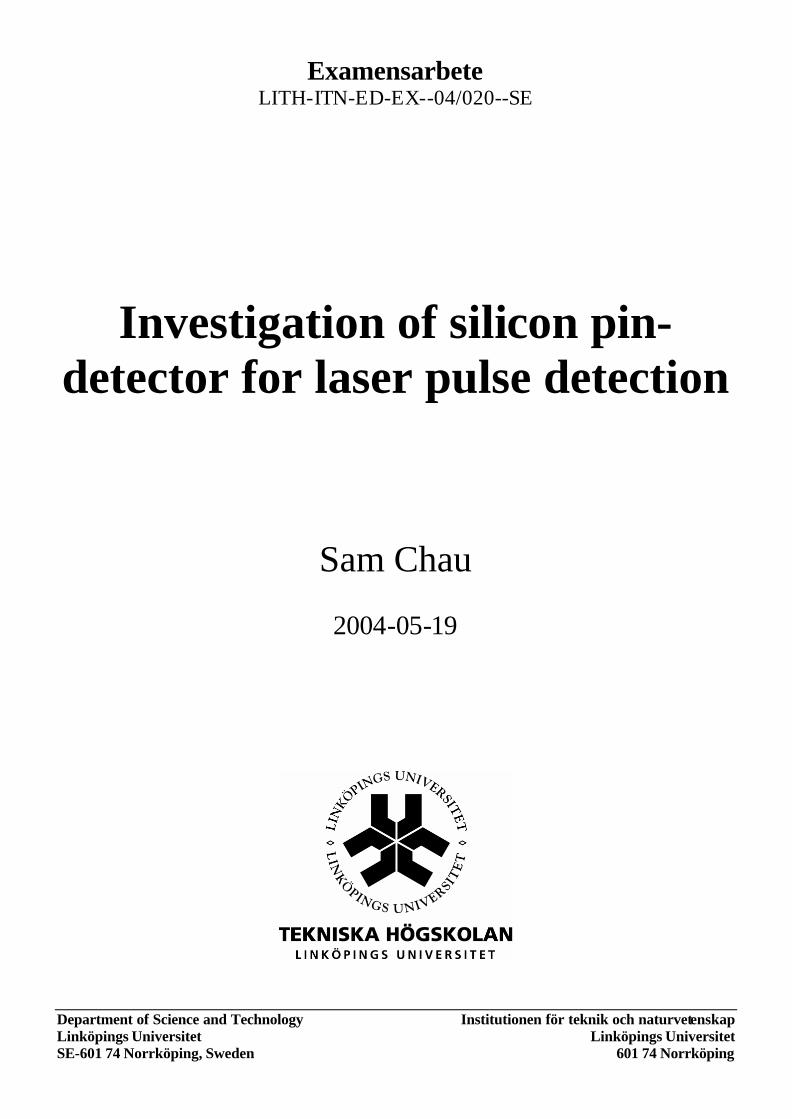
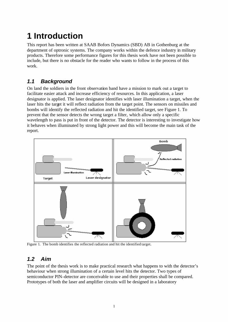
1.1 Background On land the soldiers in the front observation band have a mission to mark out a target to facilitate easier attack and increase efficiency of resources. In this application, a laser designator is applied. The laser designator identifies with laser illumination a target, when the laser hits the target it will reflect radiation from the target point. The sensors on missiles and bombs will identify the reflected radiation and hit the identified target, see Figure 1. To prevent that the sensor detects the wrong target a filter, which allow only a specific wavelength to pass is put in front of the detector. The detector is interesting to investigate how it behaves when illuminated by strong light power and this will become the main task of the report.
Figure 1. The bomb identifies the reflected radiation and hit the identified target.
1.2 Aim The point of the thesis work is to make practical research what happens to with the detector’s behaviour when strong illumination of a certain level hits the detector. Two types of semiconductor PIN-detector are conceivable to use and their properties shall be compared. Prototypes of both the laser and amplifier circuits will be designed in a laboratory

2
environment. In the amplifier circuit for the detector there is a suspicion that the amplifier will reach a saturated state. A design solution for this purpose is desired.
1.3 Limitations To be able to work with the detector in a laboratory environment, the wavelength of the laser diode was chosen to 800 nm, 10-20 ns pulse width, 10 Hz repetition frequency and power level at least 80 mW peak power. The pulse width and repetition frequency are general values in this application. Some limitations have to be set, inorder to not allow this thesis work to be too large. Some experiments should be investigated as far as time allows, e.g. detector’s properties in a higher temperature environment and testing other types of detector in comparison. A simulation program in Matlab about what bandwidth should be used was done already before this thesis work started. There is a relation between bandwidth and time constant that affects the voltage loss output at the amplifier. The limit for the time constant should be at least 5 ns, which makes total losses about 20%, from light hitting the detector into amplifier voltage output. A higher value on time constant means more loss in the electrical output signal. The limit of bandwidth should therefore be larger than 30 MHz. The loss is considered acceptable, judging from previous experience. In addition, it is only a model for the system, therefore percentual values are not very exact. Noise will arise during experiments from components, connection points and cables but it is not always possible to eliminate this noise. Noise that is not affecting the experiments in reasonable level is considered acceptable.
1.4 Method In the beginning of the work it is important to learn about how the oscilloscope is working because the whole work involves measurements from the photodetector, which deals with pulsed signals. The circuits of both the silicon-detector and the laserdiode consist of analogue electronics devices that have been designed by purchasing and assembling individual components. To make sure that protection and connection to ground works, these circuits have been assembled into metalboxes. Enclosing the circuits in metalboxes makes them less sensitive than without metalbox and has the advantage to shield from signals, which arise from external sources and in the air. A large amount of measured values have been collected and many curves have been plotted in this work. There is no necessity to use any advanced programme for this purpose, it is enough to use the programme Excel. Further, if many repetitions of the same measurement procedure shall be made the software program Labview can be applied.
3
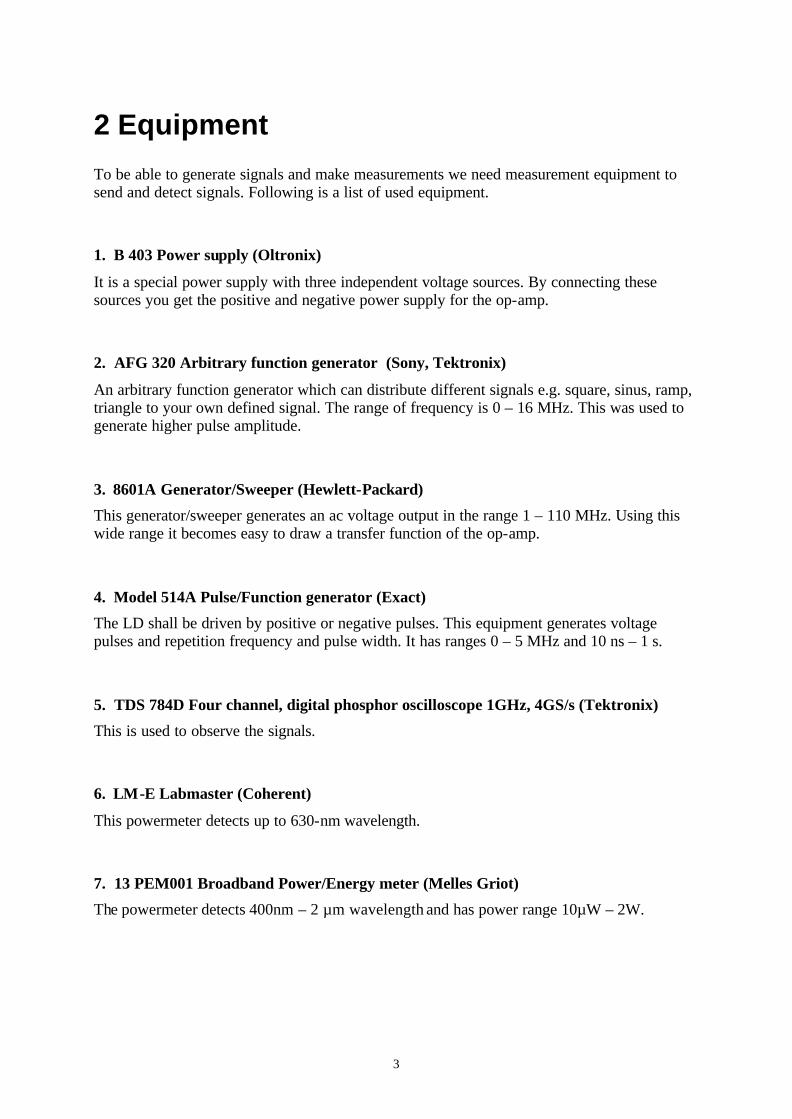
2 Equipment To be able to generate signals and make measurements we need measurement equipment to send and detect signals. Following is a list of used equipment.
1. B 403 Power supply (Oltronix)
It is a special power supply with three independent voltage sources. By connecting these sources you get the positive and negative power supply for the op-amp.
2. AFG 320 Arbitrary function generator (Sony, Tektronix)
An arbitrary function generator which can distribute different signals e.g. square, sinus, ramp, triangle to your own defined signal. The range of frequency is 0 – 16 MHz. This was used to generate higher pulse amplitude.
3. 8601A Generator/Sweeper (Hewlett-Packard)
This generator/sweeper generates an ac voltage output in the range 1 – 110 MHz. Using this wide range it becomes easy to draw a transfer function of the op-amp.
4. Model 514A Pulse/Function generator (Exact)
The LD shall be driven by positive or negative pulses. This equipment generates voltage pulses and repetition frequency and pulse width. It has ranges 0 – 5 MHz and 10 ns – 1 s.
5. TDS 784D Four channel, digital phosphor oscilloscope 1GHz, 4GS/s (Tektronix)
This is used to observe the signals.
6. LM-E Labmaster (Coherent)
This powermeter detects up to 630-nm wavelength.
7. 13 PEM001 Broadband Power/Energy meter (Melles Griot)
The powermeter detects 400nm – 2 µm wavelength and has power range 10µW – 2W.
4
3 Theory In this chapter, the fundamental components will be pointed out and described in greater detail. There are two main blocks, a sender and a receiver. The two blocks consists mainly of amplifier, photodetector, and laserdiode. The readers with good knowledge about these devices need not continue in this chapter.
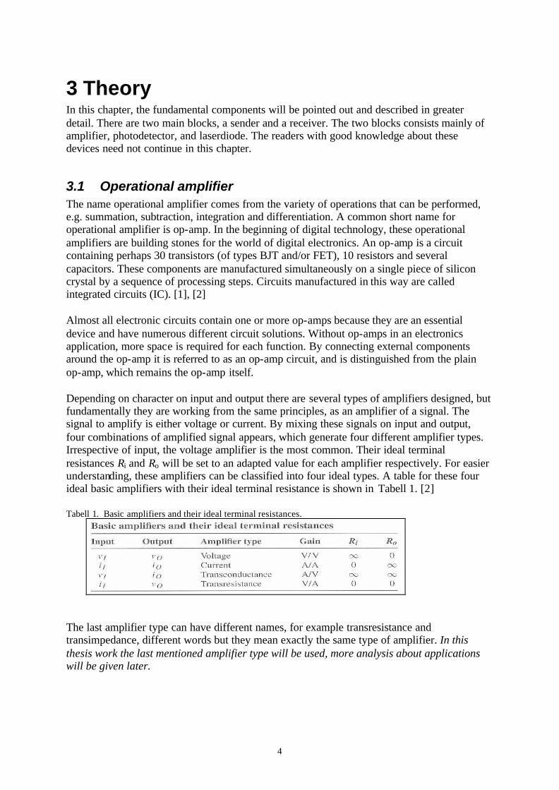
3.1 Operational amplifier The name operational amplifier comes from the variety of operations that can be performed, e.g. summation, subtraction, integration and differentiation. A common short name for operational amplifier is op-amp. In the beginning of digital technology, these operational amplifiers are building stones for the world of digital electronics. An op-amp is a circuit containing perhaps 30 transistors (of types BJT and/or FET), 10 resistors and several capacitors. These components are manufactured simultaneously on a single piece of silicon crystal by a sequence of processing steps. Circuits manufactured in this way are called integrated circuits (IC). [1], [2] Almost all electronic circuits contain one or more op-amps because they are an essential device and have numerous different circuit solutions. Without op-amps in an electronics application, more space is required for each function. By connecting external components around the op-amp it is referred to as an op-amp circuit, and is distinguished from the plain op-amp, which remains the op-amp itself. Depending on character on input and output there are several types of amplifiers designed, but fundamentally they are working from the same principles, as an amplifier of a signal. The signal to amplify is either voltage or current. By mixing these signals on input and output, four combinations of amplified signal appears, which generate four different amplifier types. Irrespective of input, the voltage amplifier is the most common. Their ideal terminal resistances Ri and Ro will be set to an adapted value for each amplifier respectively. For easier understanding, these amplifiers can be classified into four ideal types. A table for these four ideal basic amplifiers with their ideal terminal resistance is shown in Tabell 1. [2] Tabell 1. Basic amplifiers and their ideal terminal resistances.
The last amplifier type can have different names, for example transresistance and transimpedance, different words but they mean exactly the same type of amplifier. In this thesis work the last mentioned amplifier type will be used, more analysis about applications will be given later.

5
An op-amp can sometimes be treated as an ideal type, take for example an op-amp where the input impedance is very small (compared to the source) and the output impedance is very small (compared to the load), this is an approximate ideal transimpedance amplifier. [1], [2]
3.1.1 Simple op-amp structure In a real structure of the op-amp, it contains differential amplifiers (diff-amp), current mirrors and an emitter follower finally. The first mentioned is always included in an op-amp. Their purpose is to amplify the signal on the input in differential mode. Figure 2 shows how a very simple op-amp can be designed. The first couple of transistors build a differential amplifier with input in the bases and output on the collector side. A voltage difference will appear between the outputs in the first transistor couple and the ratio between the output voltage difference and the input voltage difference is called the gain. The gain will be further increased by the second transistor couple.
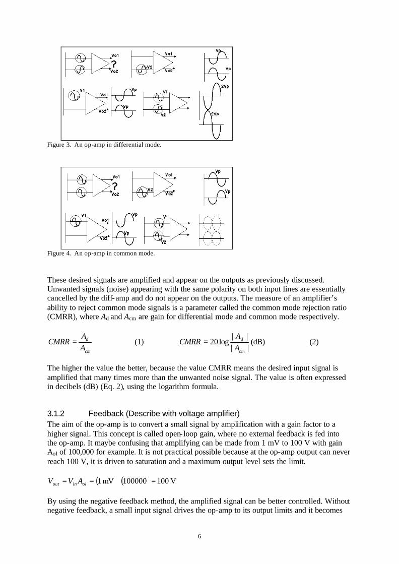
Figure 2. A simple op-amp structure. One of the most important behaviour that occurs in diff-amps is the common mode condition. If the distance from detector to amplifier is long or the amplifier is situated near a 50 Hz power cable, that may induce noise which enter as common mode disturbance. The diff-amp will amplify the desired signal but reject the noise signal because it is common mode. Two examples are shown in Figure 3 and Figure 4 about the differential mode and the common mode. [3]
6
Figure 3. An op-amp in differential mode.
Figure 4. An op-amp in common mode. These desired signals are amplified and appear on the outputs as previously discussed. Unwanted signals (noise) appearing with the same polarity on both input lines are essentially cancelled by the diff-amp and do not appear on the outputs. The measure of an amplifier’s ability to reject common mode signals is a parameter called the common mode rejection ratio (CMRR), where Ad and Acm are gain for differential mode and common mode respectively.
cm
d
AA
CMRR = (1) (dB) ||||
log20cm
d
AA
CMRR = (2)
The higher the value the better, because the value CMRR means the desired input signal is amplified that many times more than the unwanted noise signal. The value is often expressed in decibels (dB) (Eq. 2), using the logarithm formula.
3.1.2 Feedback (Describe with voltage amplifier) The aim of the op-amp is to convert a small signal by amplification with a gain factor to a higher signal. This concept is called open- loop gain, where no external feedback is fed into the op-amp. It maybe confusing that amplifying can be made from 1 mV to 100 V with gain Aol of 100,000 for example. It is not practical possible because at the op-amp output can never reach 100 V, it is driven to saturation and a maximum output level sets the limit.
( ) ( ) V 100100000mV 1 =⋅== olinout AVV By using the negative feedback method, the amplified signal can be better controlled. Without negative feedback, a small input signal drives the op-amp to its output limits and it becomes
7
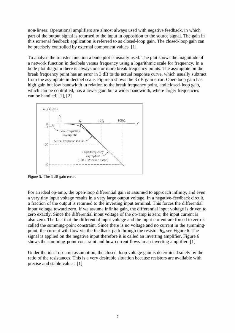
non- linear. Operational amplifiers are almost always used with negative feedback, in which part of the output signal is returned to the input in opposition to the source signal. The gain in this external feedback application is referred to as closed-loop gain. The closed-loop gain can be precisely controlled by external component values. [1] To analyse the transfer function a bode plot is usually used. The plot shows the magnitude of a network function in decibels versus frequency using a logarithmic scale for frequency. In a bode plot diagram there is always one or more break frequency points. The asymptote on the break frequency point has an error in 3 dB to the actual response curve, which usually subtract from the asymptote in decibel scale. Figure 5 shows the 3 dB gain error. Open-loop gain has high gain but low bandwidth in relation to the break frequency point, and closed- loop gain, which can be controlled, has a lower gain but a wider bandwidth, where larger frequencies can be handled. [1], [2]
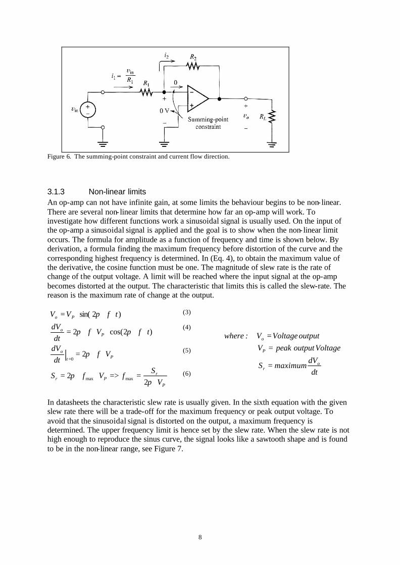
Figure 5. The 3 dB gain error. For an ideal op-amp, the open- loop differential gain is assumed to approach infinity, and even a very tiny input voltage results in a very large output voltage. In a negative-feedback circuit, a fraction of the output is returned to the inverting input terminal. This forces the differential input voltage toward zero. If we assume infinite gain, the differential input voltage is driven to zero exactly. Since the differential input voltage of the op-amp is zero, the input current is also zero. The fact that the differential input voltage and the input current are forced to zero is called the summing-point constraint. Since there is no voltage and no current in the summing-point, the current will flow via the feedback path through the resistor R2, see Figure 6. The signal is applied on the negative input therefore it is called an inverting amplifier. Figure 6 shows the summing-point constraint and how current flows in an inverting amplifier. [1] Under the ideal op-amp assumption, the closed- loop voltage gain is determined solely by the ratio of the resistances. This is a very desirable situation because resistors are available with precise and stable values. [1]
8
Figure 6. The summing-point constraint and current flow direction.
3.1.3 Non-linear limits An op-amp can not have infinite gain, at some limits the behaviour begins to be non- linear. There are several non- linear limits that determine how far an op-amp will work. To investigate how different functions work a sinusoidal signal is usually used. On the input of the op-amp a sinusoidal signal is applied and the goal is to show when the non- linear limit occurs. The formula for amplitude as a function of frequency and time is shown below. By derivation, a formula finding the maximum frequency before distortion of the curve and the corresponding highest frequency is determined. In (Eq. 4), to obtain the maximum value of the derivative, the cosine function must be one. The magnitude of slew rate is the rate of change of the output voltage. A limit will be reached where the input signal at the op-amp becomes distorted at the output. The characteristic that limits this is called the slew-rate. The reason is the maximum rate of change at the output.
P
rPr
Pt
o
Po
Po
VS
fVfS
Vfdt
dV
tfVfdt
dV
tfVV
⋅==>⋅⋅=
⋅⋅=
⋅⋅⋅⋅⋅=
⋅⋅⋅=
=
ππ
π
ππ
π
22
2
)2cos(2
)2sin(
maxmax
0|
dtdV
maximum S
Voltage output peakV output VoltageV :where
or
P
o
=
==
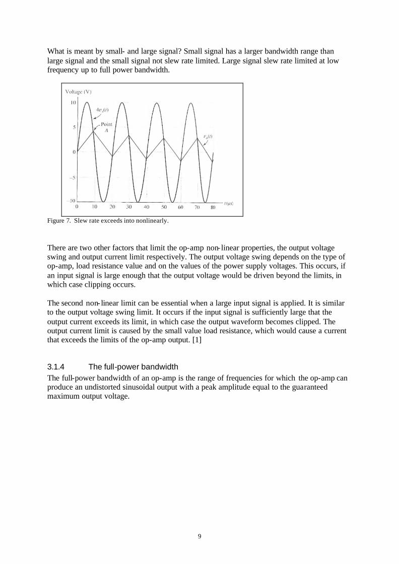
In datasheets the characteristic slew rate is usually given. In the sixth equation with the given slew rate there will be a trade-off for the maximum frequency or peak output voltage. To avoid that the sinusoidal signal is distorted on the output, a maximum frequency is determined. The upper frequency limit is hence set by the slew rate. When the slew rate is not high enough to reproduce the sinus curve, the signal looks like a sawtooth shape and is found to be in the non-linear range, see Figure 7.
(3) (4) (5) (6)
9
What is meant by small- and large signal? Small signal has a larger bandwidth range than large signal and the small signal not slew rate limited. Large signal slew rate limited at low frequency up to full power bandwidth.
Figure 7. Slew rate exceeds into nonlinearly. There are two other factors that limit the op-amp non- linear properties, the output voltage swing and output current limit respectively. The output voltage swing depends on the type of op-amp, load resistance value and on the values of the power supply voltages. This occurs, if an input signal is large enough that the output voltage would be driven beyond the limits, in which case clipping occurs. The second non- linear limit can be essential when a large input signal is applied. It is similar to the output voltage swing limit. It occurs if the input signal is sufficiently large that the output current exceeds its limit, in which case the output waveform becomes clipped. The output current limit is caused by the small value load resistance, which would cause a current that exceeds the limits of the op-amp output. [1]
3.1.4 The full-power bandwidth The full-power bandwidth of an op-amp is the range of frequencies for which the op-amp can produce an undistorted sinusoidal output with a peak amplitude equal to the guaranteed maximum output voltage.
10
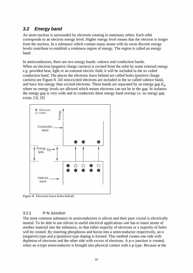
3.2 Energy band An atom nucleus is surrounded by electrons rotating in stationary orbits. Each orbit corresponds to an electron energy level. Higher energy level means that the electron is longer from the nucleus. In a substance which contain many atoms with its owns discrete energy levels contribute to establish a continuos region of energy. The region is called an energy band. In semiconductors, there are two energy bands: valence and conduction bands. When an electron (negative charge carriers) is excited from the orbit by some external energy e.g. provided heat, light or an external electric field, it will be included in the so called conduction band. The places the electrons leave behind are called holes (positive charge carriers) see Figure 8. All non-excited electrons are included in the so called valence band, and have less energy than excited electrons. These bands are separated by an energy gap Eg, where no energy levels are allowed which means electrons can not be in the gap. In isolators the energy gap is very wide and in conductors these energy band overlap i.e. no energy gap exists. [3], [9]
Figure 8. Electrons leave holes behind.
3.2.1 P-N Junction The most common substance in semiconductors is silicon and their pure crystal is electrically neutral. To be able to use silicon in useful electrical applications one has to insert atoms of another material into the substance, so that either majority of electrons or a majority of holes will be created. By inserting phosphorus and boron into a semiconductor respectively, an n (negative) type and p (positive) type doping is formed. This method creates one side with depletion of electrons and the other side with excess of electrons. A p-n junction is created, when an n-type semiconductor is brought into physical contact with a p-type. Because at the
11
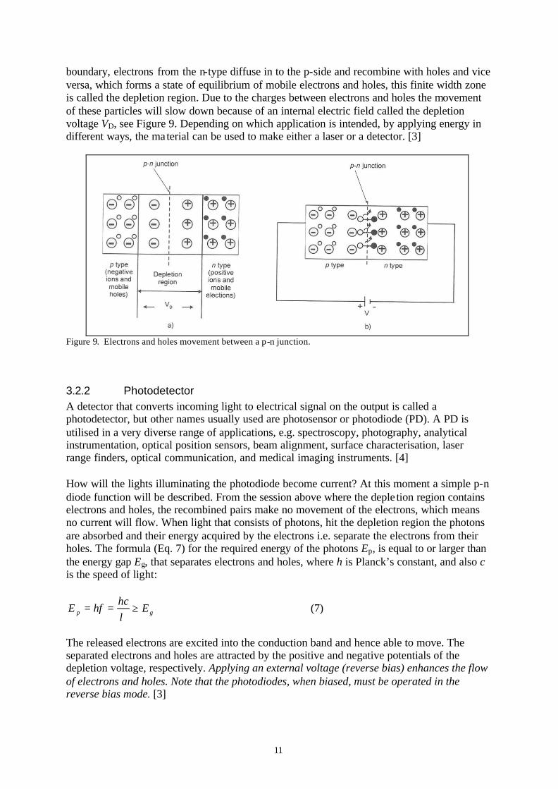
boundary, electrons from the n-type diffuse in to the p-side and recombine with holes and vice versa, which forms a state of equilibrium of mobile electrons and holes, this finite width zone is called the depletion region. Due to the charges between electrons and holes the movement of these particles will slow down because of an internal electric field called the depletion voltage VD, see Figure 9. Depending on which application is intended, by applying energy in different ways, the material can be used to make either a laser or a detector. [3]
Figure 9. Electrons and holes movement between a p-n junction.
3.2.2 Photodetector A detector that converts incoming light to electrical signal on the output is called a photodetector, but other names usually used are photosensor or photodiode (PD). A PD is utilised in a very diverse range of applications, e.g. spectroscopy, photography, analytical instrumentation, optical position sensors, beam alignment, surface characterisation, laser range finders, optical communication, and medical imaging instruments. [4] How will the lights illuminating the photodiode become current? At this moment a simple p-n diode function will be described. From the session above where the deple tion region contains electrons and holes, the recombined pairs make no movement of the electrons, which means no current will flow. When light that consists of photons, hit the depletion region the photons are absorbed and their energy acquired by the electrons i.e. separate the electrons from their holes. The formula (Eq. 7) for the required energy of the photons Ep, is equal to or larger than the energy gap Eg, that separates electrons and holes, where h is Planck’s constant, and also c is the speed of light:
gp Ehc
hfE ≥==λ
(7)
The released electrons are excited into the conduction band and hence able to move. The separated electrons and holes are attracted by the positive and negative potentials of the depletion voltage, respectively. Applying an external voltage (reverse bias) enhances the flow of electrons and holes. Note that the photodiodes, when biased, must be operated in the reverse bias mode. [3]
12
3.2.3 PIN-diode (PIN) The p-n PD has pretty limited application possibilities. There is a trade-off at the p-n PD between power and bandwidth efficiencies. Increasing the bandwidth efficiency of a p-n PD requires a wide depletion region and it is necessary to increase the reverse bias, because this voltage determines the width of the depletion region. The voltage can not be chosen arbitrarily. A wider depletion region leads to higher voltage requirements and is not comfortable since the PD is an electronic device with low-voltage supply. There are two types that improve the basic PD’s response, the avalanche photodiode (APD) and the positive- intrinsic-negative photodiode (PIN PD). The last mentioned PD has a lightly doped intrinsic layer sandwiched between thin P and N regions. The word intrinsic means “natural, undoped”. The thickness of the layer determines the depletion region in the PD, which solves the problem with increased power to achieve a wider depletion region in p-n PD. The APD is adapted for low-light conditions and high-speed requirements, having higher quantum efficiency, i.e. the magnitude of current output is larger than for a PIN PD. But the APD requires a high reverse bias and control of this bias presents significant practical difficulties. [3], [5], [6], [7]
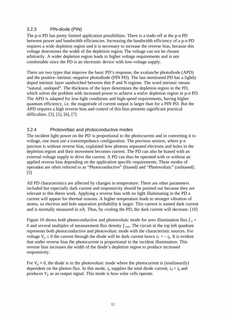
3.2.4 Photovoltaic and photoconductive modes The incident light power on the PD is proportional to the photocurrent and in converting it to voltage, one must use a transimpedance configuration. The previous session, where p-n junction is without reverse bias, explained how photons separated electrons and holes in the depletion region and their movement becomes current. The PD can also be biased with an external voltage supply to drive the current. A PD can thus be operated with or without an applied reverse bias depending on the application specific requirements. These modes of operation are often referred to as “Photoconductive” (biased) and “Photovoltaic” (unbiased). [5] All PD characteristics are affected by changes in temperature. There are other parameters included but especially dark current and responsivity should be pointed out because they are relevant to this thesis work. Applying a reverse bias with no light illuminating in the PD a current will appear for thermal reasons. A higher temperature leads to stronger vibration of atoms, so electron and hole separation probability is larger. This current is named dark current and is normally measured in nA. Thus, by cooling the PD, the dark current will decrease. [10] Figure 10 shows both photoconductive and photovoltaic mode for zero illumination flux φe = 0 and several multiples of measurement flux density φem. The circuit in the top left quadrant represents both photoconductive and photovoltaic mode with the characteristic sources. For voltage Vp ≤ 0 the current through the diode will be dark current hence iT = - ip. It is evident that under reverse bias the photocurrent is proportional to the incident illumination. This reverse bias increases the width of the diode’s depletion region to produce increased responsivity. For Vp ≈ 0, the diode is in the photovoltaic mode where the photocurrent is (nonlinearily) dependent on the photon flux. In this mode, ip supplies the total diode current, id = ip and produces Vp as an output signal. This mode is how solar cells operate.
13
Figure 10. The photodiode reproduces the basic diode curve in the photoconductive and photovoltaic mode.
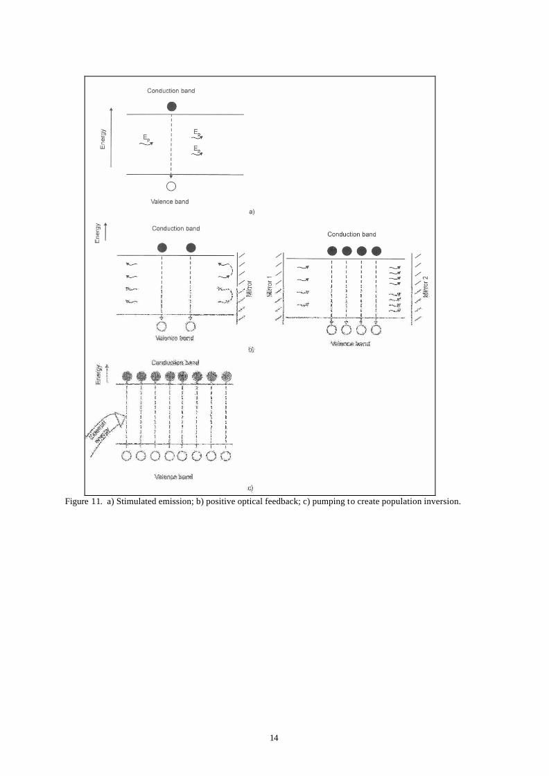
3.2.5 Laser diode (LD) The word laser is an acronym for light amplification by stimulated emission of radiation. A retrospect on the part of energy bands is in place first. Excited electrons from the conduction band fall, without any external inducement, to the valence band, which results in emission of spontaneous radiation. The properties of the spontaneous radiation are wide spectral width, low intensity, poor directivity and incoherence, this is what occurs in an LED (light emitting diode). Silicon can not be used because it does not have direct bandgap, but this is not treated here. In contrast to spontaneous radiation, stimulated radiation has narrow spectral bandwidth, high intensity (power), a high degree of directivity, and coherence. In a laser emission of stimulated radiation occurs. It means photon hits an excited electron and interacts with the electron, that transition generates a new photon see Figure 11. The induced emission stimulated by an external photon, bears the name stimulated radiation. In short ends of the LD, there are two mirrors, whose purpose is to contain the new photons by reflected between the mirrors, which further works as external photons to create new photons. This process continues infinitely during what is called positive optical feedback and the number of stimulated photons raises rapidly, see Figure 11. To drive an LD, external electrical energy “pumps” numerous electrons to an excited state, to a level that is two or three levels above the ground state. This situation is called population inversion, see Figure 11. The external energy is injected by means of a forward current. (For comparison, to make an LED emit 1 mW of output power requires up to 150 mA of forward current; a laserdiode can radiate 1 mW at 10 mA.) [3] The mirror at one end of the laser is “half-silvered,” meaning it reflects some light and lets some light through. The light that makes it through is the emitted laser light.
14
Figure 11. a) Stimulated emission; b) positive optical feedback; c) pumping to create population inversion.
15
4 System description This chapter deals with how different systems work and which devices are used including their properties. Furthermore, preparing with this information makes it easier to read the implementation chapter, thus helps the reader to get a feeling about the aim of this work. Knowledge from previous theory sessions will make the reader more familiar with the system descriptions. The thesis work as a system contains two parts, the first is the Receiver, with the PD including the op-amp circuit and the second is the Transmitter, with the LD-circuit system. To make each system work well independently is important, because that leads to advantages in easier changes for benchtest, saving time by avoiding fault searching, saving sensitive components and simplifying when the parts are put together to form the whole system. Each system is enclosed in metalboxes and holes have been drilled for mounting external connectors. The metalbox’s main property is protecting the very sensitive devices as PD and LD from electro-static discharge (ESD) and being able to mount connectors. Several advantages using metalbox are that the ground connection eliminates noise, more stable mounting on the test bench and easier change between different positions, connection using different connectors and avoiding undesired vo ltage peaks caused by the user.
4.1 Receiver The op-amp is the heart in this system. It has been chosen based on high-speed, low noise level and FET type transistors. The FET type is better and more stable than the BJT type but it is a little more expensive. There is a trade-off between cost and performance. The purchased demoboard is unpopulated and allows design of own circuitry. The PD will be mounted on the demoboard together with surface mounted components. Desirable properties of the surface mounted components are, small size, low drive voltage, low temperature drift and best of all, the properties of electric disturbance is no too high in comparison with hole mounted components. Before the PD is mounted, the characteristics of the Receiver have to be designed using the resistor and capacitor. It is easier to simulate the op-amp circuit to determine bandwidth determining the correct component values and also saving the PDs. Two variants of PD shall be tested to detect the required wavelength. The first has a peak responsivity at about 970 nm wavelength and the second has a peak responsivity at above 1000 nm wavelength. The area where the PD is sensitive to incident light is called the active area and has a size of 2.54 mm in circumference.
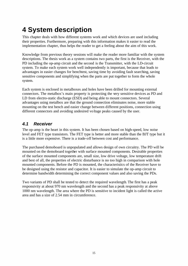
16
As discussed in Section 3.2.4, the PD shall always be used with reversed bias i.e. negative voltage applied to the anode and positive voltage to the cathode. In the characteristic of an ideal PD, there is a current generator in parallel with a capacitor and a resistor. The current generator represents the photocurrent. By using a pulse generator instead of the current generator, the experiment can be made without using PD. The source transformation is made by using Thévenin and Norton equivalent circuit analysis theorem, which is shown in Figure 12. [2]
Figure 12. Source transformation where voltage generator equivalent to current generator by Thévenin and Norton theorem.
17
4.2 Transmitter There are two types of LD used in this work the first with 635 nm and the second with 785-nm wavelength. A resistor replaced the LD in the phase of building up the system because a LD device is very sensitive and can easily break. LD II typically has 785-nm wavelength, but it has a range of wavelength between 775 – 800 nm, which is dependent on the temperature. LD I has an output power of 5 mW, which is a cheaper low-power variant used for testing before the high-power LD II is mounted. The LD is driven by dc current and in addition pulses with negative polarity that is generated by a function generator. The typically values for both the LD I and the LD II can be seen in Table 2. Table 2. The typically values for both LD.
Parameter LD I LD IILight output, Po (CW) 5 mW 80 mWThreshold current 40 mA 30 mAOperating current 55 mA 100 mAOperating voltage 2,2 V 2 VLasing wavelength 635 nm 785 nmDifferential Efficiency 0,3 mW/mA 1 mW/mA
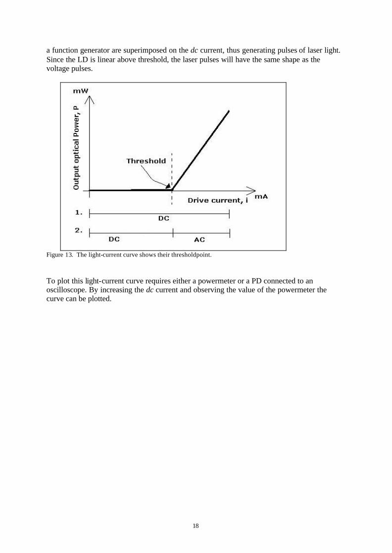
The transmitter contains an external dc circuit, based on a Laser Diode Constant Current Driver (LDCCD) that is mounted on a laboratory card and with various hole mounted components. It is called hybrid circuit when a circuit board is soldered to another circuit board. The external dc circuit supplies constant current to the LD and can be modified in different ways. One used feature is that the LDCCD provided a disable pin that allows the user to turn the LD output on or off without turning the unit’s power supply off. The advantage of this is the elimination of turn-on/turn-off transients produced by the power supply. The LD’s anode is connected to ground for added protection against ESD, which requires the LDCCD to use a negative power supply to “pull” current from the ground-referenced laser anode. For thermal management the LD is mounted in a laser case connected to the LD’s anode. [9] Several connectors and controls have been assembled in the LD box. Among these are, an external current control potentiometer which can softly turning up the current to the LD, two BNC connectors for input from function generator and output to the LD, and also connectors for digital voltmeter (DVM). On the DVM the LD current can be read, using a scale factor of 0.1 mA/mV. Increasing the dc current slowly, first the phase of spontaneous emission occurs until a threshold where stimulated emission appears. Here the LD begins to illuminate more strongly and works as a laser. In Figure 13, line 1 shows that after the thresholdpoint the output power increases proportional to the drive current. The curve is called the light-current curve and above the thresholdpoint the LD behaves linearily. Finding the thresholdpoint with high accuracy can be difficult, one method is to connect a PD to an oscilloscope in the ac mode. A small pulsed signal is superimposed on the dc drive current. When the drive current is turned up to around threshold level and the LD beam hits the photodiode, a pulse signal is seen on the oscilloscope, registered from the PD. The dc bias current is increased until the pulse signal no longer increases. The dc current is then at the threshold point. In order to create short laser pulses, the LD is driven by a dc current equal to the thresholdpoint. Short voltage pulses from
18
a function generator are superimposed on the dc current, thus generating pulses of laser light. Since the LD is linear above threshold, the laser pulses will have the same shape as the voltage pulses.
Figure 13. The light-current curve shows their thresholdpoint. To plot this light-current curve requires either a powermeter or a PD connected to an oscilloscope. By increasing the dc current and observing the value of the powermeter the curve can be plotted.
19
5 Implementation A demoboard in the form of an unpopulated printed circuit board (PCB) was used for the Receiver. Using unpopulated board several circuit solutions have been tested. All details and how the formulas are used may not always be possible to show, but in this chapter the circuit solutions are basically explained and determination of component values is shown. This section treats the implementation of the Receiver and Transmitter, connection between them and the systemintegration i.e. how it works with real components.
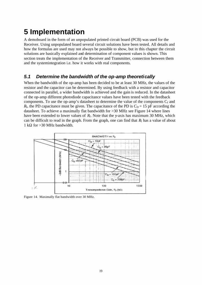
5.1 Determine the bandwidth of the op-amp theoretically When the bandwidth of the op-amp has been decided to be at least 30 MHz, the values of the resistor and the capacitor can be determined. By using feedback with a resistor and capacitor connected in parallel, a wider bandwidth is achieved and the gain is reduced. In the datasheet of the op-amp different photodiode capacitance values have been tested with the feedback components. To use the op-amp’s datasheet to determine the value of the components Cf and Rf, the PD capacitance must be given. The capacitance of the PD is CD = 15 pF according the datasheet. To achieve a maximally flat bandwidth for >30 MHz see Figure 14 where lines have been extended to lower values of Rf. Note that the y-axis has maximum 30 MHz, which can be difficult to read in the graph. From the graph, one can find that Rf has a value of about 1 kΩ for >30 MHz bandwidth.
Figure 14. Maximally flat bandwidth over 30 MHz.
20
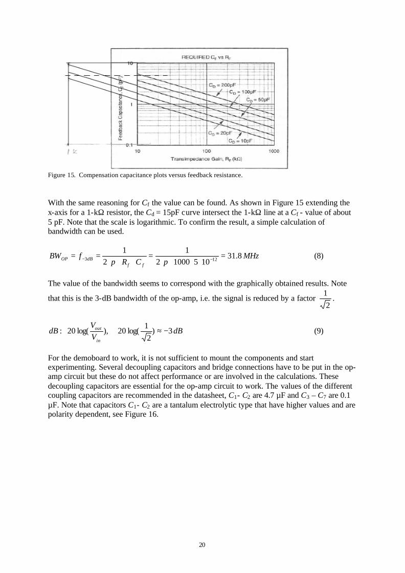
Figure 15. Compensation capacitance plots versus feedback resistance. With the same reasoning for Cf the value can be found. As shown in Figure 15 extending the x-axis for a 1-kΩ resistor, the Cd = 15pF curve intersect the 1-kΩ line at a Cf - value of about 5 pF. Note that the scale is logarithmic. To confirm the result, a simple calculation of bandwidth can be used.
MHzCR
fBWff
dBOP 8.3110510002
12
1123 =
⋅⋅⋅⋅=
⋅⋅⋅== −− ππ
(8)
The value of the bandwidth seems to correspond with the graphically obtained results. Note
that this is the 3-dB bandwidth of the op-amp, i.e. the signal is reduced by a factor 2
1.
dBVV
dBin
out 3)2
1log( 20 ),log( 02 : −≈ (9)
For the demoboard to work, it is not sufficient to mount the components and start experimenting. Several decoupling capacitors and bridge connections have to be put in the op-amp circuit but these do not affect performance or are involved in the calculations. These decoupling capacitors are essential for the op-amp circuit to work. The values of the different coupling capacitors are recommended in the datasheet, C1- C2 are 4.7 µF and C3 – C7 are 0.1 µF. Note that capacitors C1- C2 are a tantalum electrolytic type that have higher values and are polarity dependent, see Figure 16.
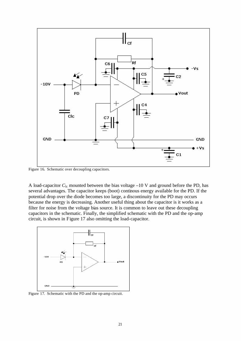
21
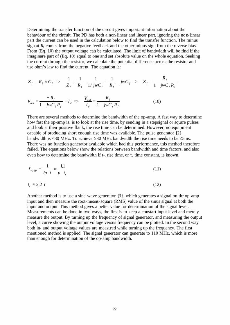
Figure 16. Schematic over decoupling capacitors. A load-capacitor Clc mounted between the bias voltage –10 V and ground before the PD, has several advantages. The capacitor keeps (boot) continous energy available for the PD. If the potential drop over the diode becomes too large, a discontinuity for the PD may occurs because the energy is decreasing. Another useful thing about the capacitor is it works as a filter for noise from the voltage bias source. It is common to leave out these decoupling capacitors in the schematic. Finally, the simplified schematic with the PD and the op-amp circuit, is shown in Figure 17 also omitting the load-capacitor.
Figure 17. Schematic with the PD and the op-amp circuit.
22
Determining the transfer function of the circuit gives important information about the behaviour of the circuit. The PD has both a non- linear and linear part, ignoring the non- linear part the current can be used in the calculation below to find the transfer function. The minus sign at Rf comes from the negative feedback and the other minus sign from the reverse bias. From (Eq. 10) the output voltage can be calculated. The limit of bandwidth will be find if the imaginare part of (Eq. 10) equal to one and set absolute value on the whole equation. Seeking the current through the resistor, we calculate the potential difference across the resistor and use ohm’s law to find the current. The equation is:
ff
fff
fffffff RCj
RZCj
RCjRZCRZ
ωω
ω +==>+=+==>=
1
1/1
111 //
1
1 ff
f
d
outd
ff
fout RCj
R
IV
IRCj
RV
ωω +==>−⋅
+
−= (10)
There are several methods to determine the bandwidth of the op-amp. A fast way to determine how fast the op-amp is, is to look at the rise time, by sending in a stepsignal or square pulses and look at their positive flank, the rise time can be determined. However, no equipment capable of producing short enough rise time was available. The pulse generator 2 bandwidth is <30 MHz. To achieve ≥30 MHz bandwidth the rise time needs to be ≤5 ns. There was no function generator available which had this performance, this method therefore failed. The equations below show the relations between bandwidth and time factors, and also even how to determine the bandwidth if tr, rise time, or τ, time constant, is known.
r3
1,12
1t
f dB ⋅≈
⋅=− πτπ
(11)
τ⋅≈ 2,2rt (12)
Another method is to use a sine-wave generator 3, which generates a signal on the op-amp input and then measure the root-means-square (RMS) value of the sinus signal at both the input and output. This method gives a better value for determination of the signal level. Measurements can be done in two ways, the first is to keep a constant input level and merely measure the output. By turning up the frequency of signal generator, and measuring the output level, a curve showing the output voltage versus frequency can be plotted. In the second way both in- and output voltage values are measured while turning up the frequency. The first mentioned method is applied. The signal generator can generate to 110 MHz, which is more than enough for determination of the op-amp bandwidth.
23
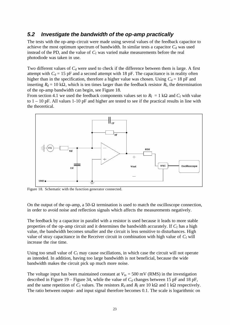
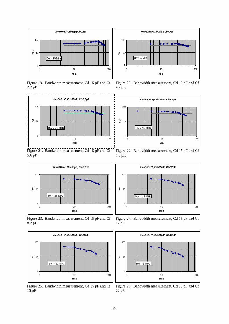
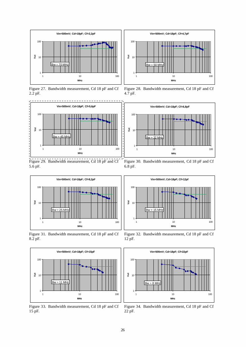
5.2 Investigate the bandwidth of the op-amp practically The tests with the op-amp-circuit were made using several values of the feedback capacitor to achieve the most optimum spectrum of bandwidth. In similar tests a capacitor Cd was used instead of the PD, and the value of Cf was varied make measurements before the real photodiode was taken in use. Two different values of Cd were used to check if the difference between them is large. A first attempt with Cd = 15 pF and a second attempt with 18 pF. The capacitance is in reality often higher than in the specification, therefore a higher value was chosen. Using Cd = 18 pF and inserting Rd = 10 kΩ, which is ten times larger than the feedback resistor Rf, the determination of the op-amp bandwidth can begin, see Figure 18. From section 4.1 we used the feedback components values set to Rf = 1 kΩ and Cf with value to 1 – 10 pF. All values 1-10 pF and higher are tested to see if the practical results in line with the theoretical.
Figure 18. Schematic with the function generator connected. On the output of the op-amp, a 50-Ω termination is used to match the oscilloscope connection, in order to avoid noise and reflection signals which affects the measurements negatively. The feedback by a capacitor in parallel with a resistor is used because it leads to more stable properties of the op-amp circuit and it determines the bandwidth accurately. If Cf has a high value, the bandwidth becomes smaller and the circuit is less sensitive to disturbances. High value of stray capacitance in the Receiver circuit in combination with high value of Cf will increase the rise time. Using too small value of Cf may cause oscillations, in which case the circuit will not operate as intended. In addition, having too large bandwidth is not beneficial, because the wide bandwidth makes the circuit pick up much more noise. The voltage input has been maintained constant at Vin = 500 mV (RMS) in the investigation described in Figure 19 – Figure 34, while the value of Cd changes between 15 pF and 18 pF, and the same repetition of Cf values. The resistors Rd and Rf are 10 kΩ and 1 kΩ respectively. The ratio between output- and input signal therefore becomes 0.1. The scale is logarithmic on
24
both axes. The horizontal lines in Figure 19 – Figure 34 marks out the level at –3 dB of the
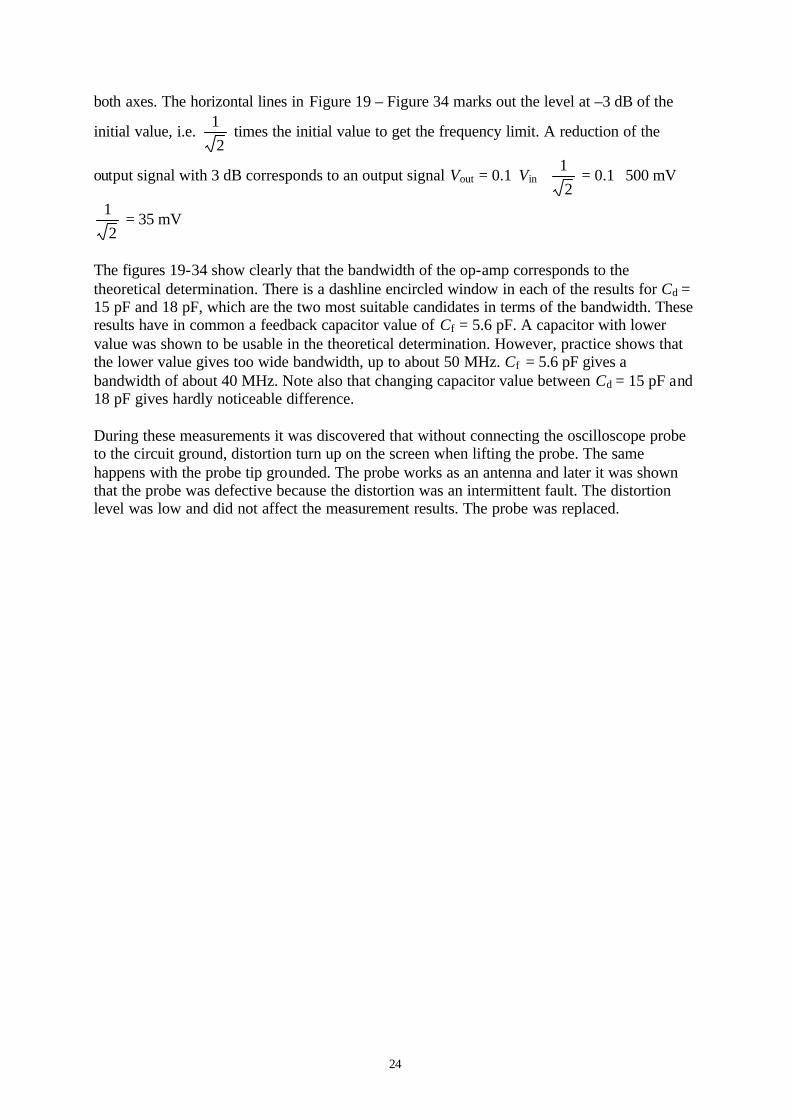
initial value, i.e. 2
1 times the initial value to get the frequency limit. A reduction of the
output signal with 3 dB corresponds to an output signal Vout = 0.1⋅ Vin ⋅ 2
1 = 0.1 ⋅ 500 mV ⋅
21
= 35 mV
The figures 19-34 show clearly that the bandwidth of the op-amp corresponds to the theoretical determination. There is a dashline encircled window in each of the results for Cd = 15 pF and 18 pF, which are the two most suitable candidates in terms of the bandwidth. These results have in common a feedback capacitor value of Cf = 5.6 pF. A capacitor with lower value was shown to be usable in the theoretical determination. However, practice shows that the lower value gives too wide bandwidth, up to about 50 MHz. Cf = 5.6 pF gives a bandwidth of about 40 MHz. Note also that changing capacitor value between Cd = 15 pF and 18 pF gives hardly noticeable difference. During these measurements it was discovered that without connecting the oscilloscope probe to the circuit ground, distortion turn up on the screen when lifting the probe. The same happens with the probe tip grounded. The probe works as an antenna and later it was shown that the probe was defective because the distortion was an intermittent fault. The distortion level was low and did not affect the measurement results. The probe was replaced.
25
Vin=500mV; Cd=15pf; Cf=2,2pF
1
10
100
1 10 100
MHz
Vu
t
Bw = 70 MHz
Vin=500mV; Cd=15pF; Cf=4,7pF
1
10
100
1 10 100
MHz
Vu
t
Bw = 50 MHz
Figure 19. Bandwidth measurement, Cd 15 pF and Cf 2.2 pF.
Figure 20. Bandwidth measurement, Cd 15 pF and Cf 4.7 pF.
Vin=500mV; Cd=15pF; Cf=5,6pF
1
10
100
1 10 100
MHz
Vu
t
Bw = 42 MHz
Vin=500mV; Cd=15pF; Cf=6,8pF
1
10
100
1 10 100
MHz
Vu
t
Bw = 32 MHz
Figure 21. Bandwidth measurement, Cd 15 pF and Cf 5.6 pF.
Figure 22. Bandwidth measurement, Cd 15 pF and Cf 6.8 pF.
Vin=500mV; Cd=15pF; Cf=8,2pF
1
10
100
1 10 100
MHz
Vu
t
Bw = 25 MHz
Vin=500mV; Cd=15pF; Cf=12pF
1
10
100
1 10 100
MHz
Vu
t
Bw = 15 MHz
Figure 23. Bandwidth measurement, Cd 15 pF and Cf 8.2 pF.
Figure 24. Bandwidth measurement, Cd 15 pF and Cf 12 pF.
Vin=500mV; Cd=15pF; Cf=15pF
1
10
100
1 10 100
MHz
Vu
t
Bw = 11 MHz
Vin=500mV; Cd=15pF; Cf=22pF
1
10
100
1 10 100
MHz
Vu
t
Bw = 8 MHz
Figure 25. Bandwidth measurement, Cd 15 pF and Cf 15 pF.
Figure 26. Bandwidth measurement, Cd 15 pF and Cf 22 pF.
26
Vin=500mV; Cd=18pF; Cf=2,2pF
1
10
100
1 10 100
MHz
Vu
t
Bw = 70 MHz
Vin=500mV; Cd=18pF; Cf=4,7pF
1
10
100
1 10 100
MHz
Vu
t
Bw = 50 MHz
Figure 27. Bandwidth measurement, Cd 18 pF and Cf 2.2 pF.
Figure 28. Bandwidth measurement, Cd 18 pF and Cf 4.7 pF.
Vin=500mV; Cd=18pF; Cf=5,6pF
1
10
100
1 10 100
MHz
Vu
t
Bw = 45 MHz
Vin=500mV; Cd=18pF; Cf=6,8pF
1
10
100
1 10 100
MHz
Vu
t
Bw = 32 MHz
Figure 29. Bandwidth measurement, Cd 18 pF and Cf 5.6 pF.
Figure 30. Bandwidth measurement, Cd 18 pF and Cf 6.8 pF.
Vin=500mV; Cd=18pF; Cf=8,2pF
1
10
100
1 10 100
MHz
Vu
t
Bw = 25 MHz
Vin=500mV; Cd=18pF; Cf=12pf
1
10
100
1 10 100
MHz
Vu
t
Bw = 15 MHz
Figure 31. Bandwidth measurement, Cd 18 pF and Cf 8.2 pF.
Figure 32. Bandwidth measurement, Cd 18 pF and Cf 12 pF.
Vin=500mV; Cd=18pF; Cf=15pF
1
10
100
1 10 100
MHz
Vu
t
Bw = 11 MHz
Vin=500mV; Cd=18pF; Cf=22pF
1
10
100
1 10 100
MHz
Vu
t
Bw = 8 MHz
Figure 33. Bandwidth measurement, Cd 18 pF and Cf 15 pF.
Figure 34. Bandwidth measurement, Cd 18 pF and Cf 22 pF.
27
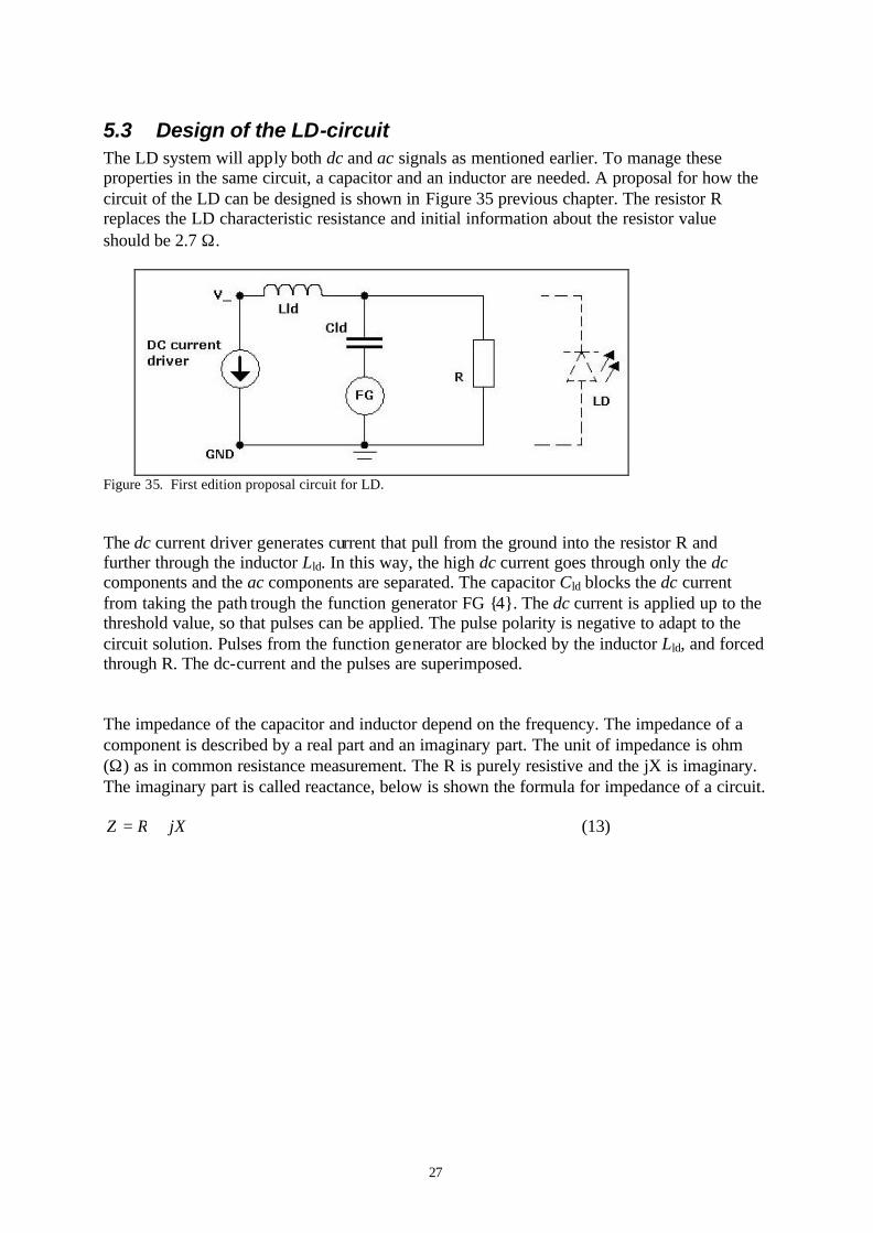
5.3 Design of the LD-circuit The LD system will apply both dc and ac signals as mentioned earlier. To manage these properties in the same circuit, a capacitor and an inductor are needed. A proposal for how the circuit of the LD can be designed is shown in Figure 35 previous chapter. The resistor R replaces the LD characteristic resistance and initial information about the resistor value should be 2.7 Ω.
Figure 35. First edition proposal circuit for LD. The dc current driver generates current that pull from the ground into the resistor R and further through the inductor Lld. In this way, the high dc current goes through only the dc components and the ac components are separated. The capacitor Cld blocks the dc current from taking the path trough the function generator FG 4. The dc current is applied up to the threshold value, so that pulses can be applied. The pulse polarity is negative to adapt to the circuit solution. Pulses from the function generator are blocked by the inductor Lld, and forced through R. The dc-current and the pulses are superimposed. The impedance of the capacitor and inductor depend on the frequency. The impedance of a component is described by a real part and an imaginary part. The unit of impedance is ohm (Ω) as in common resistance measurement. The R is purely resistive and the jX is imaginary. The imaginary part is called reactance, below is shown the formula for impedance of a circuit.
jXRZ += (13)
28
For these components the real part R is negligible The equations for these imaginary parts are as follows:
Capacitor: =>=Cj
jX C ω1
fCC
ZC πω 211
== (14)
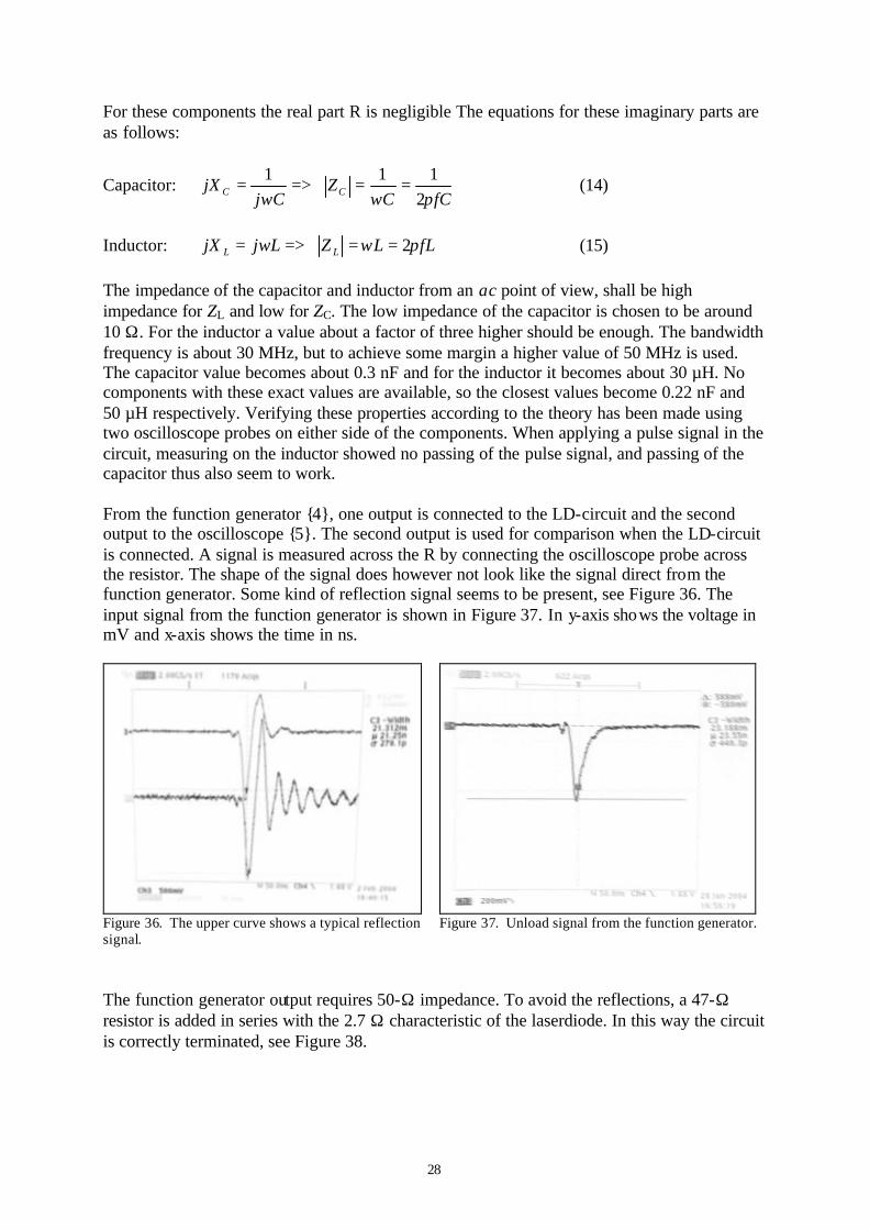
Inductor: =>= LjjX L ω fLLZ L πω 2== (15) The impedance of the capacitor and inductor from an ac point of view, shall be high impedance for ZL and low for ZC. The low impedance of the capacitor is chosen to be around 10 Ω. For the inductor a value about a factor of three higher should be enough. The bandwidth frequency is about 30 MHz, but to achieve some margin a higher value of 50 MHz is used. The capacitor value becomes about 0.3 nF and for the inductor it becomes about 30 µH. No components with these exact values are available, so the closest values become 0.22 nF and 50 µH respectively. Verifying these properties according to the theory has been made using two oscilloscope probes on either side of the components. When applying a pulse signal in the circuit, measuring on the inductor showed no passing of the pulse signal, and passing of the capacitor thus also seem to work. From the function generator 4, one output is connected to the LD-circuit and the second output to the oscilloscope 5. The second output is used for comparison when the LD-circuit is connected. A signal is measured across the R by connecting the oscilloscope probe across the resistor. The shape of the signal does however not look like the signal direct from the function generator. Some kind of reflection signal seems to be present, see Figure 36. The input signal from the function generator is shown in Figure 37. In y-axis shows the voltage in mV and x-axis shows the time in ns.
Figure 36. The upper curve shows a typical reflection signal.
Figure 37. Unload signal from the function generator.
The function generator output requires 50-Ω impedance. To avoid the reflections, a 47-Ω resistor is added in series with the 2.7 Ω characteristic of the laserdiode. In this way the circuit is correctly terminated, see Figure 38.
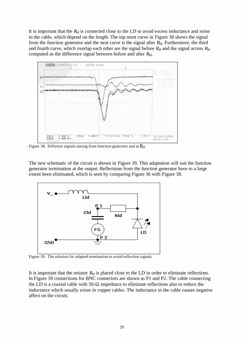
29
It is important that the Rld is connected close to the LD to avoid excess inductance and noise in the cable, which depend on the length. The top most curve in Figure 38 shows the signal from the function generator and the next curve is the signal after Rld. Furthermore, the third and fourth curve, which overlap each other are the signal before Rld and the signal across Rld computed as the difference signal between before and after Rld.
Figure 38. Different signals among from function generator and at Rld. The new schematic of the circuit is shown in Figure 39. This adaptation will suit the function generator termination at the output. Reflections from the function generator have to a large extent been eliminated, which is seen by comparing Figure 36 with Figure 38.
Figure 39. The solution for adapted termination to avoid reflection signals. It is important that the resistor Rld is placed close to the LD in order to eliminate reflections. In Figure 39 connections for BNC connectors are shown as P1 and P2. The cable connecting the LD is a coaxial cable with 50-Ω impedance to eliminate reflections also to reduce the inductance which usually exists in copper cables. The inductance in the cable causes negative affect on the circuit.
30
5.4 Responsivity Both the Transmitter and Receiver have now been designed, now in this section the main task of this project will be described, the measurement of PD, responsivity. The goal is to describe the behaviour of the entire system, from incident light into the PD to the voltage signal out. The responsivity is a measure of the effectiveness of the conversion of light power into electrical current. The definition of the responsivity of a silicon photodiode is the ratio of the photocurrent IP to the incident light power P at a given wavelength. Furthermore, these properties depend on temperature and applied reverse bias. However, see measurements the temperature is not taken into account because the laboratory environment provided a stable temperature interval so the effect is negligible. [4]
PI
R P=λ (16)
λRRP
IRP
VWVainceiver F
PFout ⋅=⋅
==)/( g Re (17)
Equation 17 describes the Receiver gain and how to find the responsivity Rλ, where RF is the feedback resistor and Vout is the voltage output of the amplifier. Before a measurement of the PD responsivity can be made, focusing of the LD radiation must be done. The LD is driven above threshold by dc current and a dc signal is registered on the Receiver. Furthermore, the LD is mounted in a fixture which can move in the two lateral dimensions. By moving the LD laterally one can verify that the illumination is in the active area or outside the PD. The focusing will be easy to do. When the beam pattern becomes approximately the same size as the PD, it will not look like a circle. Instead, it has more the shape of oval geometric figure with a sharp middle line. The distance between the detector and the LD does not matter because it does not affect the light-power. These stepwise instructions on how to compute the responsivity begin with the Transmitter and continue with the Receiver. LD This method uses an optical powermeter in dc mode. Apply the LD dc current from zero to maximum value that the LD is capable of and simultaneously plot a curve of registered output light power as a function of the dc current, read off on the DVM. The part near the threshold where the pulsing occur, on the LD light-current curve is the most interesting. Keep reference to zero at the threshold and step dc-current to the maximum value, thus obtaining a new axis scale with zero at the threshold. Draw a new light-current curve that only contains the gradient-line with the same power axis towards the new current axis. Compute the gradient of the light-current curve. The coefficient has no special name. In datasheets it is usually called differential efficiency. The differential efficiency = dPo/dIop (W/A) shows the effectiveness of the input current conversion to light power. A comparison between the received result and the nominal value i.e. the value in the datasheet will show if the result is reasonable. Measurements using the Receiver do not need a powermeter, instead the function generator and an oscilloscope is used. In this part we will use the differential efficiency measured previously, to compute the output power from the Transmitter. The linearity of the gradient
31
assures that the light output follows the shape of the input voltage pulse. The goal is to obtain a responsivity value of the PD near to the nominal value. PD The function generator generates negative pulses with 20-30 ns pulse width and 10 Hz repetition frequency achieve an exact value is impossible due to the function generator adjustment. Adjusting the pulse amplitude at the function generator, the measurements of voltage in (Vin) over the resistor Rld and the output voltage (Vout) from the amplifier will be registered. By using ohm’s law i.e. divide Vin on the Rld value, the pulse current is obtained. The next step is to calculate the optical power by using the differential efficiency coefficiency determined previously. Multiplying it with the previously calculated current, the optical pulse peak power is found. This method has to be used because the powermeter can not register the short pulse. Finally plot a curve showing the output voltage as a function of the incident optical-power. The gradient is the responsivity of the PD. These steps have been repeated numerous times to test different values of components and other adjustments. The temperature can be considered constant at room temperature. The LD has been driven for long periods of time and has reached a higher equilibrium temperature. In the next chapter the results will be shown.
32
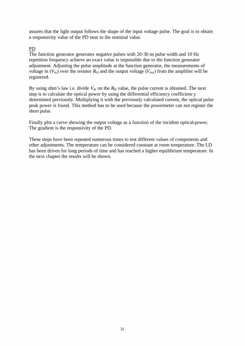
6 Results Two laserdiodes will be used in the experiments. The LD with lower output power is used first to get a feeling for what the pulses and curves look like. The methods have been described in section 4.4, which makes it easier to follow the coming results and comments. The behaviour of the PD is investigated in this section, by plotting curves that show the linearity of the behaviour. In this section many curves will appear. Two photodiodes were intended to be tested. However due to unknown reasons it was not possible to do that, more about this in the text. The tested PD is of the type Planar Diffused Silicon PD, PIN-5D manufactured by UDT, and a peak responsivity wavelength, λP of 970 nm i.e. a typically value of 0.65 A/W at 970-nm wavelength, as in Figure 40. The responsivity at 635 nm and 785 nm wavelength corresponding to the LD wavelengths, can be found in Figure 40, to be 0.4 A/W at 635 nm and 0.58 A/W at 785 nm.
Figure 40. Typically characteristic of responsivity for 635 nm and 785 nm wavelength on this PD.
6.1 The LD with 635-nm wavelength In the beginning, the Transmitter beam was tightly focused to a small dot on the PD. Focusing the optical power to such a small area can make a mark in the PD and the optical power is not smoothly distributed over the active area, which can lead to the measurement errors. Changing the dot to a spot, which almost fills up the active area is better for measurements. The colour of the beam is red and the maximum output power level is 5 mW. Some component values need to bear in mind before presenting the result curves. In section 5.3, the R is set to about 2.7 Ω believed to be the LD characteristic resistance. To adapt this to the oscilloscope input, the resistor Rld was set to 47 Ω and during measurement, two probes were applied across Rld. The termination of the oscilloscope is 50 Ω. In the Receiver, see Figure 16, the component values Cf = 5.6 pF and Rf = 1 kΩ was used in the beginning, note that this will change later.
33
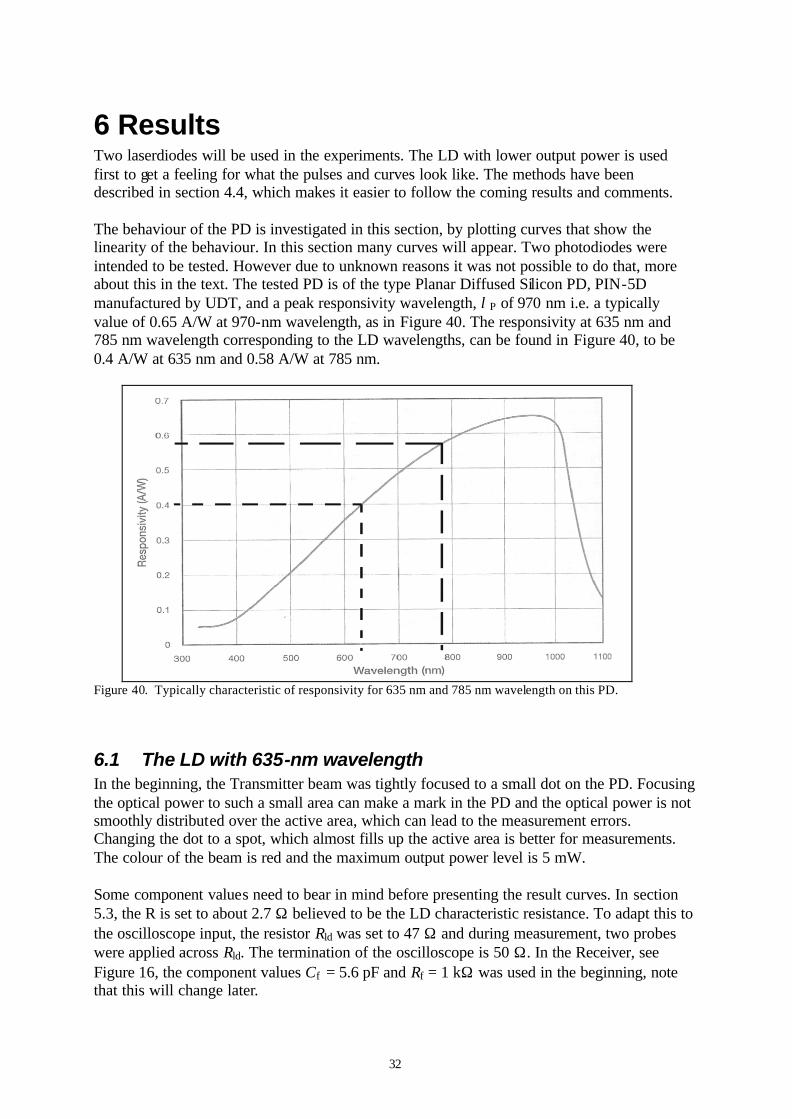
Applying the dc current in the Transmitter, a current-to-power curve is plotted by detecting the optical power with the powermeter 6 and also the PD, see Figure 41. It shows how well the Receiver follows the powermeter, and that the Receiver is working as expected.
635 nm, Output Power vs Current (light-current curve), DC
0
0,5
1
1,5
2
2,5
3
3,5
4
4,5
0 3 6 9 12 15 18 21 24 27 30 33
Current, mA
Out
put
Pow
er, m
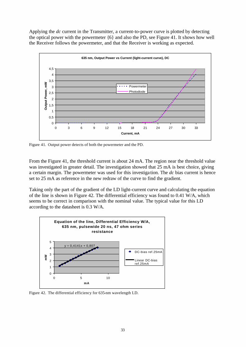
W
Powermeter
Photodiode
Figure 41. Output power detects of both the powermeter and the PD. From the Figure 41, the threshold current is about 24 mA. The region near the threshold value was investigated in greater detail. The investigation showed that 25 mA is best choice, giving a certain margin. The powermeter was used for this investiga tion. The dc bias current is hence set to 25 mA as reference in the new redraw of the curve to find the gradient. Taking only the part of the gradient of the LD light-current curve and calculating the equation of the line is shown in Figure 42. The differential efficiency was found to 0.41 W/A, which seems to be correct in comparison with the nominal value. The typical value for this LD according to the datasheet is 0.3 W/A.
Equation of the line, Differential Efficiency W/A, 635 nm, pulsewide 20 ns, 47 ohm series
resistance
y = 0,4141x + 0,807
0
1
2
3
4
5
0 5 10
mA
mW
DC-bias ref.25mA
Linear DC-biasref.25mA
Figure 42. The differential efficiency for 635-nm wavelength LD.
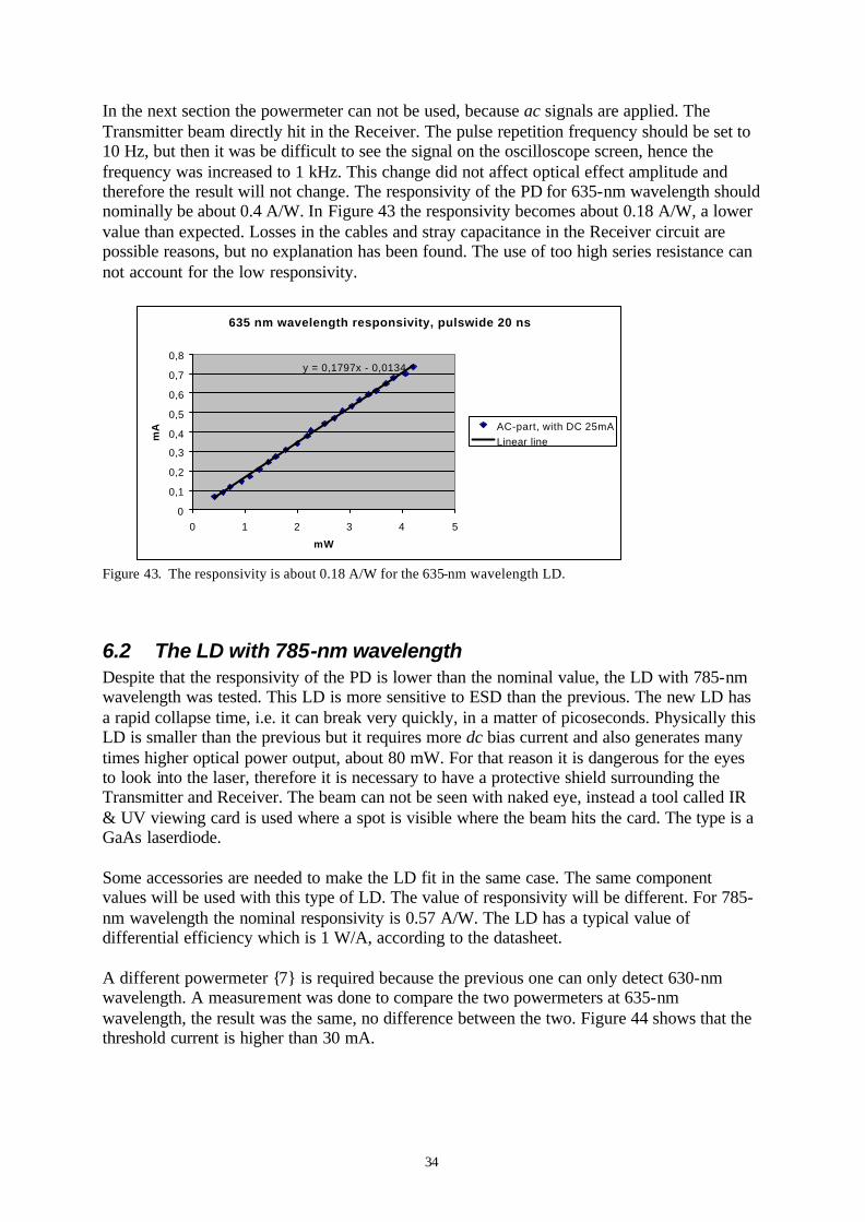
34
In the next section the powermeter can not be used, because ac signals are applied. The Transmitter beam directly hit in the Receiver. The pulse repetition frequency should be set to 10 Hz, but then it was be difficult to see the signal on the oscilloscope screen, hence the frequency was increased to 1 kHz. This change did not affect optical effect amplitude and therefore the result will not change. The responsivity of the PD for 635-nm wavelength should nominally be about 0.4 A/W. In Figure 43 the responsivity becomes about 0.18 A/W, a lower value than expected. Losses in the cables and stray capacitance in the Receiver circuit are possible reasons, but no explanation has been found. The use of too high series resistance can not account for the low responsivity.
635 nm wavelength responsivity, pulswide 20 ns
y = 0,1797x - 0,0134
0
0,1
0,2
0,3
0,4
0,5
0,6
0,7
0,8
0 1 2 3 4 5
mW
mA AC-part, with DC 25mA
Linear line
Figure 43. The responsivity is about 0.18 A/W for the 635-nm wavelength LD.
6.2 The LD with 785-nm wavelength Despite that the responsivity of the PD is lower than the nominal value, the LD with 785-nm wavelength was tested. This LD is more sensitive to ESD than the previous. The new LD has a rapid collapse time, i.e. it can break very quickly, in a matter of picoseconds. Physically this LD is smaller than the previous but it requires more dc bias current and also generates many times higher optical power output, about 80 mW. For that reason it is dangerous for the eyes to look into the laser, therefore it is necessary to have a protective shield surrounding the Transmitter and Receiver. The beam can not be seen with naked eye, instead a tool called IR & UV viewing card is used where a spot is visible where the beam hits the card. The type is a GaAs laserdiode. Some accessories are needed to make the LD fit in the same case. The same component values will be used with this type of LD. The value of responsivity will be different. For 785-nm wavelength the nominal responsivity is 0.57 A/W. The LD has a typical value of differential efficiency which is 1 W/A, according to the datasheet. A different powermeter 7 is required because the previous one can only detect 630-nm wavelength. A measurement was done to compare the two powermeters at 635-nm wavelength, the result was the same, no difference between the two. Figure 44 shows that the threshold current is higher than 30 mA.
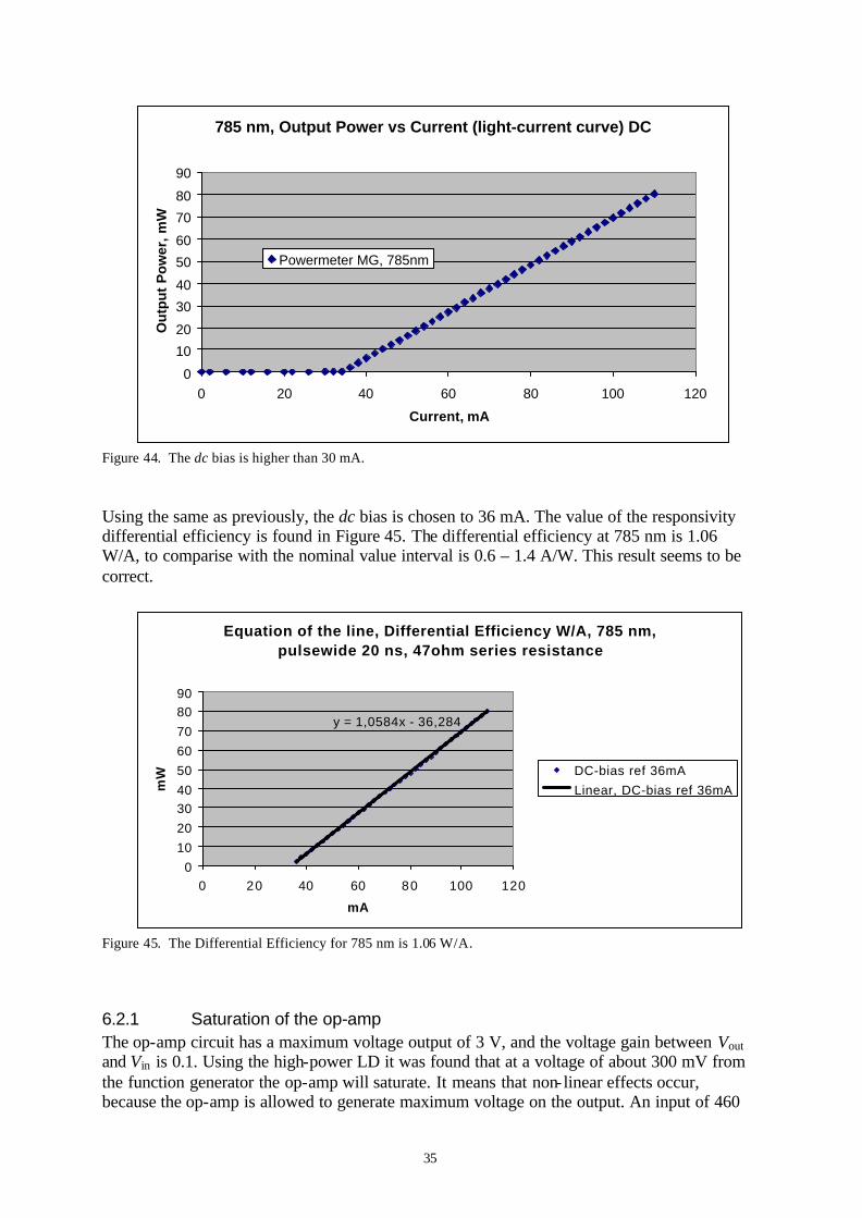
35
785 nm, Output Power vs Current (light-current curve) DC
0
10
20
30
40
50
60
70
80
90
0 20 40 60 80 100 120
Current, mA
Ou
tpu
t P
ow
er, m
W
Powermeter MG, 785nm
Figure 44. The dc bias is higher than 30 mA. Using the same as previously, the dc bias is chosen to 36 mA. The value of the responsivity differential efficiency is found in Figure 45. The differential efficiency at 785 nm is 1.06 W/A, to comparise with the nominal value interval is 0.6 – 1.4 A/W. This result seems to be correct.
Equation of the line, Differential Efficiency W/A, 785 nm, pulsewide 20 ns, 47ohm series resistance
y = 1,0584x - 36,284
0102030405060708090
0 20 40 60 80 100 120
mA
mW DC-bias ref 36mA
Linear, DC-bias ref 36mA
Figure 45. The Differential Efficiency for 785 nm is 1.06 W/A.
6.2.1 Saturation of the op-amp The op-amp circuit has a maximum voltage output of 3 V, and the voltage gain between Vout and Vin is 0.1. Using the high-power LD it was found that at a voltage of about 300 mV from the function generator the op-amp will saturate. It means that non- linear effects occur, because the op-amp is allowed to generate maximum voltage on the output. An input of 460
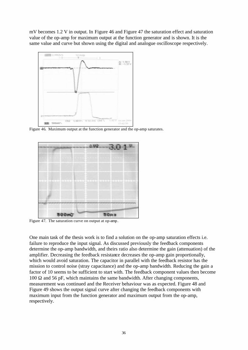
36
mV becomes 1.2 V in output. In Figure 46 and Figure 47 the saturation effect and saturation value of the op-amp for maximum output at the function generator and is shown. It is the same value and curve but shown using the digital and analogue oscilloscope respectively.
Figure 46. Maximum output at the function generator and the op-amp saturates.
Figure 47. The saturation curve on output at op-amp. One main task of the thesis work is to find a solution on the op-amp saturation effects i.e. failure to reproduce the input signal. As discussed previously the feedback components determine the op-amp bandwidth, and theirs ratio also determine the gain (attenuation) of the amplifier. Decreasing the feedback resistance decreases the op-amp gain proportionally, which would avoid saturation. The capacitor in parallel with the feedback resistor has the mission to control noise (stray capacitance) and the op-amp bandwidth. Reducing the gain a factor of 10 seems to be sufficient to start with. The feedback component values then become 100 Ω and 56 pF, which maintains the same bandwidth. After changing components, measurement was continued and the Receiver behaviour was as expected. Figure 48 and Figure 49 shows the output signal curve after changing the feedback components with maximum input from the function generator and maximum output from the op-amp, respectively.
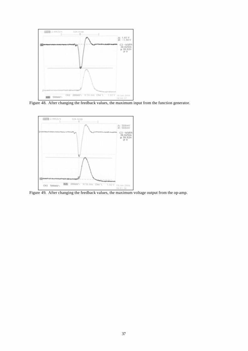
37
Figure 48. After changing the feedback values, the maximum input from the function generator.
Figure 49. After changing the feedback values, the maximum voltage output from the op-amp.
38
6.2.2 Wire-wound type resistor Calculations show that, the power does not reach 80 mW. The maximum attainable output power is 29 mW. One idea to overcome this is to reduce the Rld value to half and check if the output voltage increases to double of its. Table 3 shows the input voltage and the output voltage for two different values of the resistance Rld. Table 3. Voltage over Rld with two different values, show on output voltage.
Vin (mV) Vout, Rld = 22ohm (mV) Vout, Rld = 47ohm (mV)100 34 51150 76 86,5200 107 115,5250 138 133300 164 165350 189 193400 226 222450 261 255500 292 286
The test shows that the function generator cannot achieve higher output voltage. To achieve higher optical power the series resistance can be decreased. First, a resistor of less than half the resistance, 22 Ω, is used and the result generates questions because the output level does not differ as much twice. A closer investigation about the resistor type is made because of a suspicion that it may be important. The resistor used is a wire-wound type, which has bad high-frequency properties. Other resistor types are made of massive carbon or metal film. The best type for high frequencies is the surface mount type because the small size does not induce so much inductance. The inductance creates disturbance, which can be difficult to control so it is important to decrease the inductance as much as possible. The strange phenomena observed can most likely be explained by the use of the wire-wound type resistor. Another possible explanation can be the cable length, longer cables have more inductance. Below in Figure 50 and Figure 51 is shown the responsivity for different values on the wire-wound type resistor. In one case the outputpower is close to 60 mW and the behaviour seems quite linear but the properties may be unstable because of the resistor type. This is one of the reasons not to continue on this track.
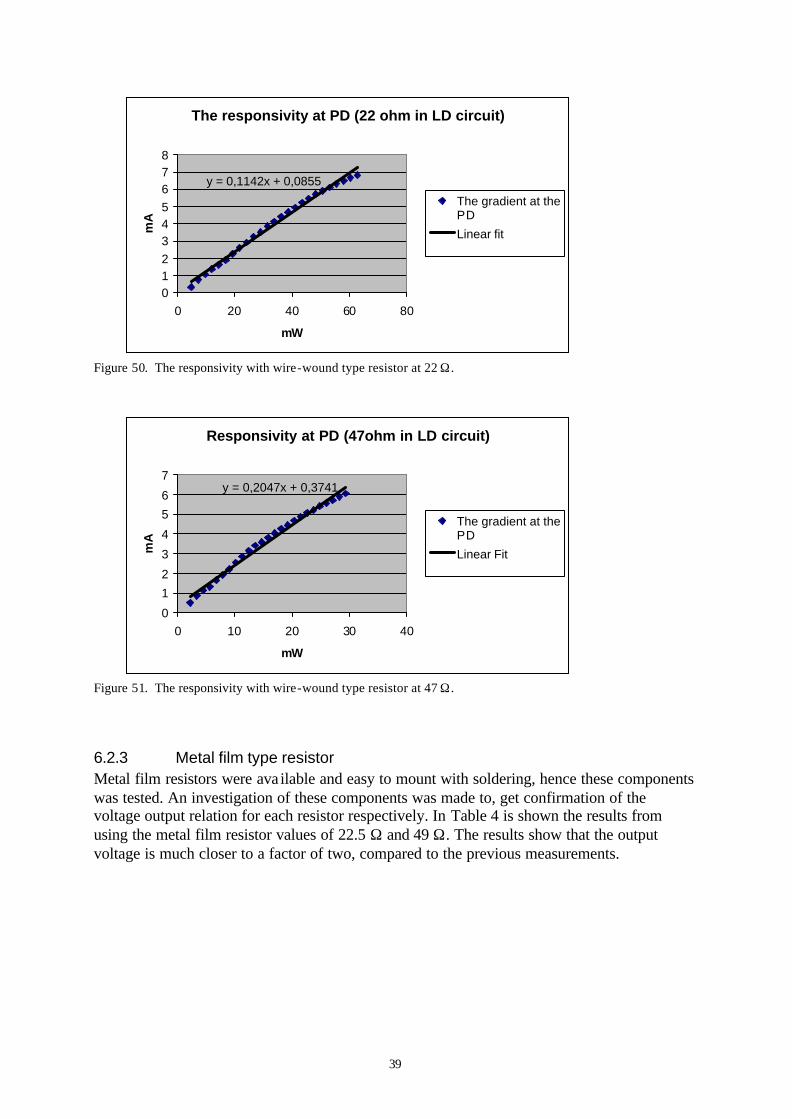
39
The responsivity at PD (22 ohm in LD circuit)
y = 0,1142x + 0,0855
012345678
0 20 40 60 80
mW
mA
The gradient at thePD
Linear fit
Figure 50. The responsivity with wire-wound type resistor at 22 Ω .
Responsivity at PD (47ohm in LD circuit)
y = 0,2047x + 0,3741
0
1
2
3
4
5
6
7
0 10 20 30 40
mW
mA
The gradient at thePD
Linear Fit
Figure 51. The responsivity with wire-wound type resistor at 47 Ω .
6.2.3 Metal film type resistor Metal film resistors were ava ilable and easy to mount with soldering, hence these components was tested. An investigation of these components was made to, get confirmation of the voltage output relation for each resistor respectively. In Table 4 is shown the results from using the metal film resistor values of 22.5 Ω and 49 Ω. The results show that the output voltage is much closer to a factor of two, compared to the previous measurements.
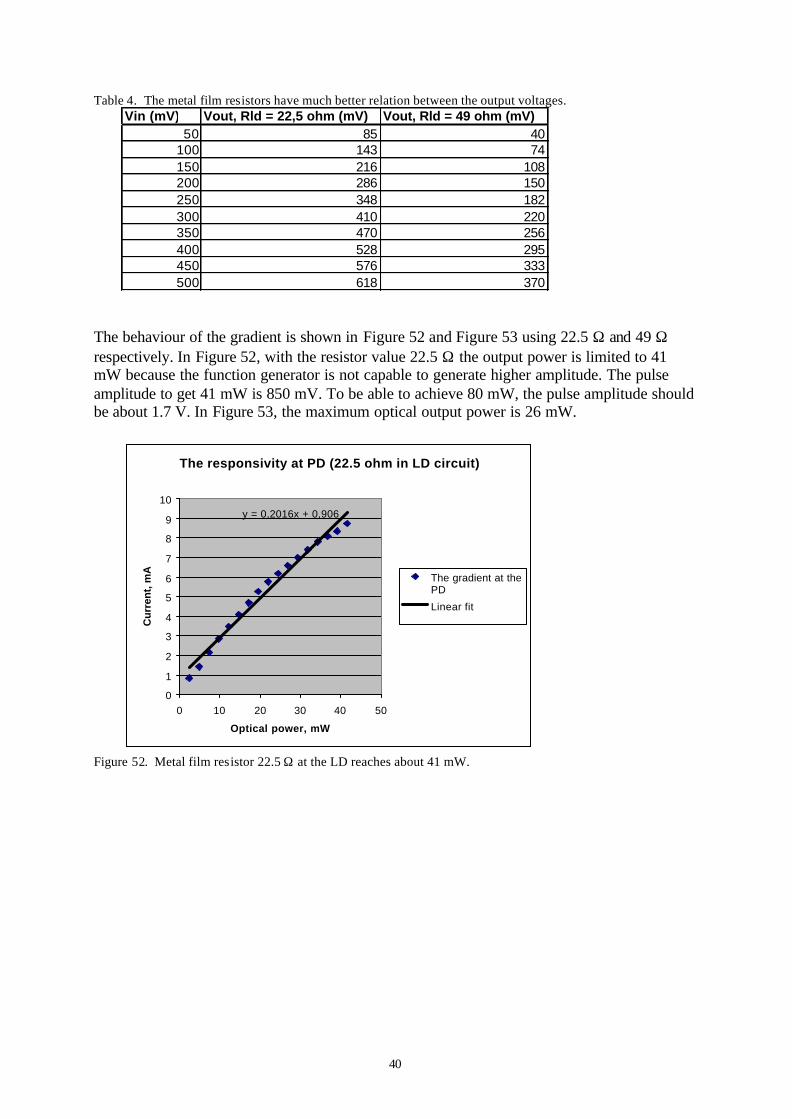
40
Table 4. The metal film resistors have much better relation between the output voltages.
Vin (mV) Vout, Rld = 22,5 ohm (mV) Vout, Rld = 49 ohm (mV)50 85 40
100 143 74150 216 108200 286 150250 348 182300 410 220350 470 256400 528 295450 576 333500 618 370
The behaviour of the gradient is shown in Figure 52 and Figure 53 using 22.5 Ω and 49 Ω respectively. In Figure 52, with the resistor value 22.5 Ω the output power is limited to 41 mW because the function generator is not capable to generate higher amplitude. The pulse amplitude to get 41 mW is 850 mV. To be able to achieve 80 mW, the pulse amplitude should be about 1.7 V. In Figure 53, the maximum optical output power is 26 mW.
The responsivity at PD (22.5 ohm in LD circuit)
y = 0,2016x + 0,906
0
1
2
3
4
5
6
7
8
9
10
0 10 20 30 40 50
Optical power, mW
Cur
rent
, mA
The gradient at thePD
Linear fit
Figure 52. Metal film resistor 22.5 Ω at the LD reaches about 41 mW.
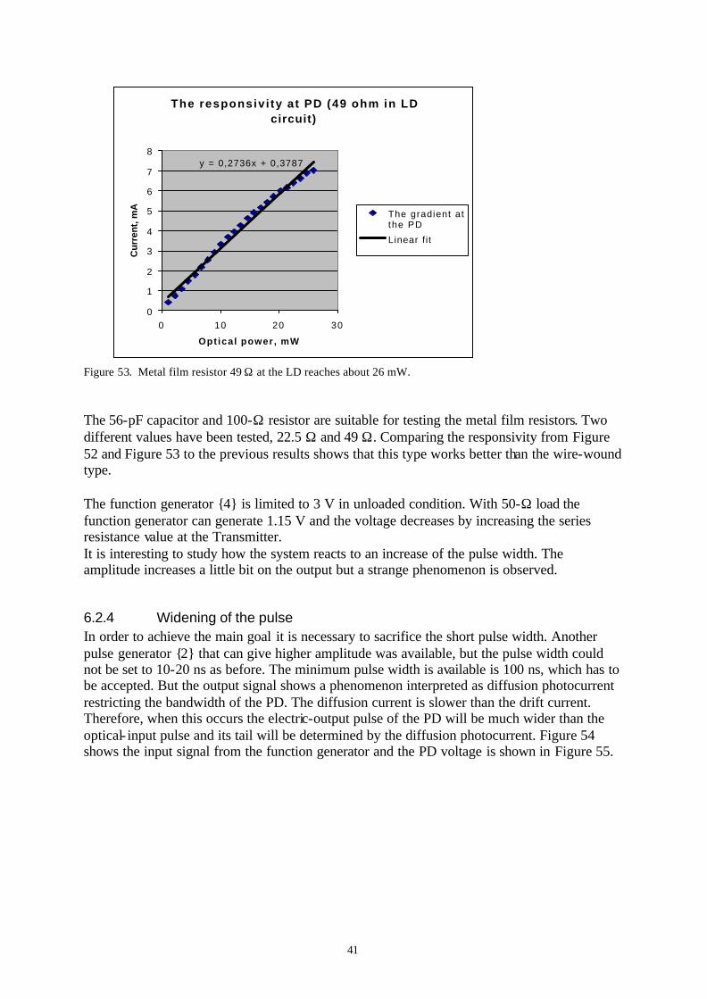
41
The responsivi ty at PD (49 ohm in LD circuit)
y = 0,2736x + 0,3787
0
1
2
3
4
5
6
7
8
0 10 20 30
Optical power, mW
Cur
rent
, mA
The gradient atthe PD
Linear fit
Figure 53. Metal film resistor 49 Ω at the LD reaches about 26 mW. The 56-pF capacitor and 100-Ω resistor are suitable for testing the metal film resistors. Two different values have been tested, 22.5 Ω and 49 Ω. Comparing the responsivity from Figure 52 and Figure 53 to the previous results shows that this type works better than the wire-wound type. The function generator 4 is limited to 3 V in unloaded condition. With 50-Ω load the function generator can generate 1.15 V and the voltage decreases by increasing the series resistance value at the Transmitter. It is interesting to study how the system reacts to an increase of the pulse width. The amplitude increases a little bit on the output but a strange phenomenon is observed.
6.2.4 Widening of the pulse In order to achieve the main goal it is necessary to sacrifice the short pulse width. Another pulse generator 2 that can give higher amplitude was available, but the pulse width could not be set to 10-20 ns as before. The minimum pulse width is available is 100 ns, which has to be accepted. But the output signal shows a phenomenon interpreted as diffusion photocurrent restricting the bandwidth of the PD. The diffusion current is slower than the drift current. Therefore, when this occurs the electric-output pulse of the PD will be much wider than the optical- input pulse and its tail will be determined by the diffusion photocurrent. Figure 54 shows the input signal from the function generator and the PD voltage is shown in Figure 55.
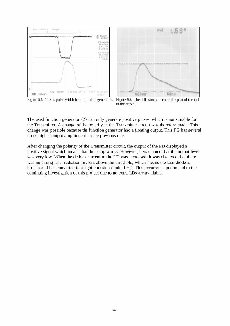
42
Figure 54. 100 ns pulse width from function generator. Figure 55. The diffusion current is the part of the tail
in the curve. The used function generator 2 can only generate positive pulses, which is not suitable for the Transmitter. A change of the polarity in the Transmitter circuit was therefore made. This change was possible because the function generator had a floating output. This FG has several times higher output amplitude than the previous one. After changing the polarity of the Transmitter circuit, the output of the PD displayed a positive signal which means that the setup works. However, it was noted that the output level was very low. When the dc bias current to the LD was increased, it was observed that there was no strong laser radiation present above the threshold, which means the laserdiode is broken and has converted to a light emission diode, LED. This occurrence put an end to the continuing investigation of this project due to no extra LDs are available.
43
7 Discussion From Figures 19-34, the bandwidth and different components values can be determined. Practical measurements showed that the bandwidth is determined by the feedback capacitor to a larger value than expected. The PD characteristic capacitance affects the feedback capacitor value. In bandwidth determination experiments the value of Cd changes between 15 pF and 18 pF and tests are repeated with different values of Cf. The resistors Rd and Rf are 10 Ω and 1 kΩ respectively. The values of the feedback components are settled to 5.6 pF in parallel with 1 kΩ that the bandwidth becomes about 45 MHz. With a lower value on the feedback capacitor, the bandwidth becomes too high. According to the datasheet of the op-amp it will saturate 3 V, which was proven in practice with the high power LD. The solution to avoid saturation is to change the feedback values to 10 times lower gain on the output while keeping the ratio between the capacitor and resistor constant. Furthermore, the op-amp does not saturate after these changes, which is an advantage for the following simulations. The design of the Transmitter was successful in permitting the use of both dc and ac current. The inductor and capacitor values were chosen with the ac frequency in mind. The functions that were designed into the Transmitter to conduct the ac and dc currents along different paths worked well. The basic model of the Transmitter introduced distortion and was redesigned with a loop to eliminate of the reflection signals. By adapting the correct of 50 Ω at the oscilloscope connectors the reflection signals could be controlled. The resistors of wire-wound type could not be used due to the high inductance, which depend on frequency and temperature, that causing non- linear behaviour in comparison with different values at the resistors of the op-amp’s voltage output. Using metal film or metal oxided hole mounted types instead, measurements show a more linear behaviour. Towards the end of the test, a surface-mount resistor was successfully mounted near the LD, which without doubt had the best properties of the three tested resistor types. The maximum optical power achieved, of the possible 80 mW of the LD, is about 40 mW. The curve behaves certainly linear. What will happen with the behaviour of the PD at higher power is difficult to say, based on these measurements. The pulse amplitude was limited and dependent on the load, for the first used function generator. This affected the experiments negatively but it had the advantage that a short pulse width was achievable, which the second function generator did not have. The second function generator generated higher amplitude but could only produce positive pulses, which meant the polarity connections on the Transmitter had to be changed. The change of polarity seems to be working since the PD gives a response on the oscilloscope screen. The response resembles the previous curve shape and it is a certain indication that this method can be used. However, at this moment when all instruments are prepared for testing at higher power, the LD fails and behaves as an LED. It is the sign of a broken laser diode. Totally two laser diodes have been broken. The first one broke at an earlier moment because the power supply to the Transmitter was not disconnected over a weekend, which may have caused a voltage spike through the LD. The new function generator’s higher amplitude may have broken the second LD, if the amplitude has been turned up too high. It could also have been caused by other causes, e.g. loose connections, but this has not been investigated and

44
will not be further discussed. To order new laser diodes takes several months, therefore further experiments can not be done.
45
8 Future work and improvements Although the new function generator has a minimum pulse width of 100 ns it is interesting to use it to investigate the behaviour of the PD. Another method is to further reduce the value of the LD series resistor to achieve 80 mW, but the reflection signals will dominate and it can be difficult to interpret the results. Measurements using the surface mounted resistor is one of the other things which ought to be tested. There is a better method to test the Transmitter, by replacing the LD with a resistor after every change. Arbitrary values can be achieved and above all many LDs will be saved from destruction, for example by unexpected peak voltages. The differential efficiency of the LD is temperature dependent, so it would be advantageous to control the temperature of the LD. Towards the end of the work a surface mounted resistor was successfully soldered close to the LD, but at this time the LD had ceased to work. It would be very interesting to compare different resistor types to see the difference. Another type of PD was available for measurements but because of the mishap with the LD the adventure ended. It would have been interesting to compare the two PDs and evaluate the difference in detection properties. The environment, primarily higher temperatures, can affect the behaviour of the PD and it was one of the goals in this investigation but for obvious reasons this can not be achieved. The most important observation has not been mentioned so much, which is the responsivity of the PD. Regardless of the value of the LD series resistor, with correct focusing and direction, all radiation should fall on the PD. With respect to the previous factors, the responsivity value should be the same for different optical power levels. Furthermore, the measured value of responsivity is lower than in the specification. Since the responsivity is temperature dependent, the temperature of the PD could be monitored or stablized in order to achieve more accurate results. The equation (Eq. 10) with the transfer function is for the ideal transimpedance amplifier, which suggests that the frequency response is strictly due to the feedback network. To be able, to investigate the instability properties e.g. oscillations in the circuit, the components characteristics should be modeled by using for example an ideal current source in parallel with its equivalent resistance and capacitance. This transfer function is more comprehensive than the previous one and the noise gain of this configuration determines the stability of the circuit. The reason for this is that any noise signal, no matter how small, can trigger an unstable circuit into oscillation. This is a suggestion for further work if one comes into contact with the oscillation problems. [11] If a choice of PD is available there are several advantages by choosing a smaller size of PD. The junction capacitance in the PD should be as low as possible because it affects not only the bandwidth but also the noise as well. [12] The PD active area should be as small as possible so that the junction capacitance is small and the junction resistance is high. This will allow a higher signal-to-noise ratio i.e. the noise is reduced and a higher signal is allowed. If a large area is needed, this can be supplied by using optical gain (lens, mirror, etc.). Optical “gain” is essentially noise-free. [12]

46
In the earlier session going from a short pulse to a wider pulse of 100 ns the shape resembles a square pulse and on the output curve a “tail” is observed, caused by the slower diffusion current. By using higher reverse bias the junction capacitance will reduced and also eliminate or reduce the slow fall time of the diffusion “tail”.

47
9 References Literature references 1. Sergio Franco, Design with operational amplifiers and analog integrated circuits, Third edition The McGraw-Hill Companies, 2002 ISBN: 0-07-112173-0 2. Allan R. Hambley, Electrical engineering, principles and applications second edition Prentice-Hall inc, 2001 ISBN: 0-131-061070-4 3. Djafar K. Mynbaev & Lowell L. Scheiner, Fiber-Optic Communications Technology Prentice-Hall inc, 2001 ISBN: 0-13-962069-9 4. Thomas L. Floyd, Basic operational amplifiers and linear integrated circuits Macmillan Publishing Company, 1994 ISBN: 0-02-338641-X 5. UDT Sensors, Inc 2003 Optoelectronic Components Catalog An OSI Systems Company 6. Jerald Graeme, Photodiode amplifiers OP AMP SOLUTIONS McGraw-Hill, 1995 ISBN: 0-07-024247-X 7. Robert Tell, Torbjö rn Andersson, Per Andersson, Fiberoptisk kommunikationsteknik – kopmponenter och
vågutbredning, Studentlitteratur 1990, Andra upplagan, ISBN: 91-44-26202-7 8. Handbook, Thorlabs Model LD1255 Laser Diode Constant Current Driver Website references 9. http://www.isk.kth.se/kursinfo/6b2344/diod/diod.doc 2004-03-17 10. http://www.biox.kth.se/kjellinternet/Bildfystenta.02.del1.1.PDF 2004-03-17 11. http://manuales.elo.utfsm.cl/datasheet/burr-brown/PDFFILES/AP-NOTES/AB-050.pdf 2004-03-17 12. http://www.ai.mit.edu/people/leinad/PHOTOS/275/photodiode-amplifiers-burr-brown-notes.pdf 2004-03-17
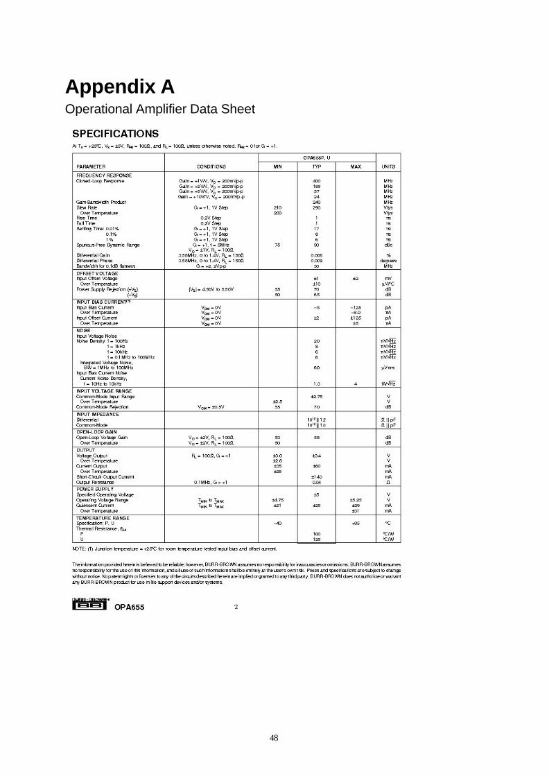
48
Appendix A Operational Amplifier Data Sheet
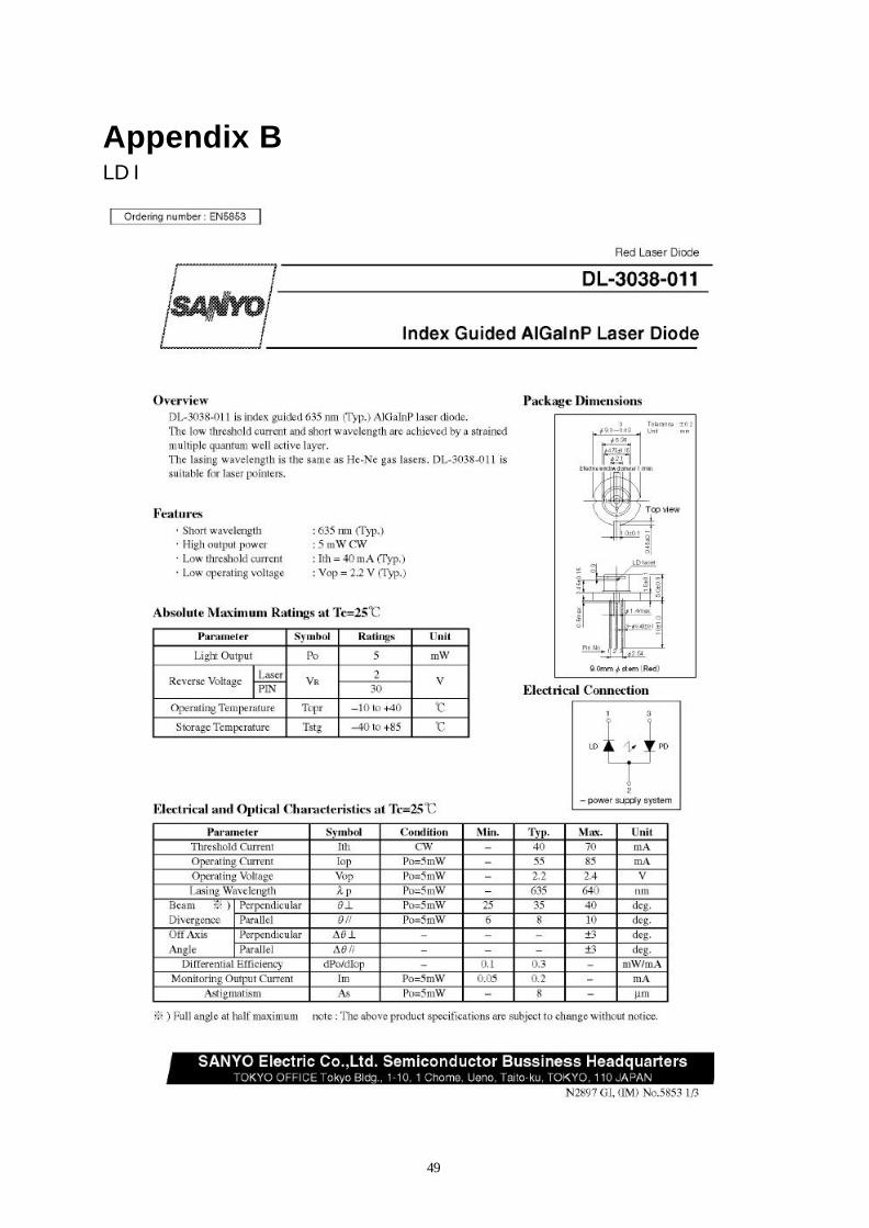
49
Appendix B LD I
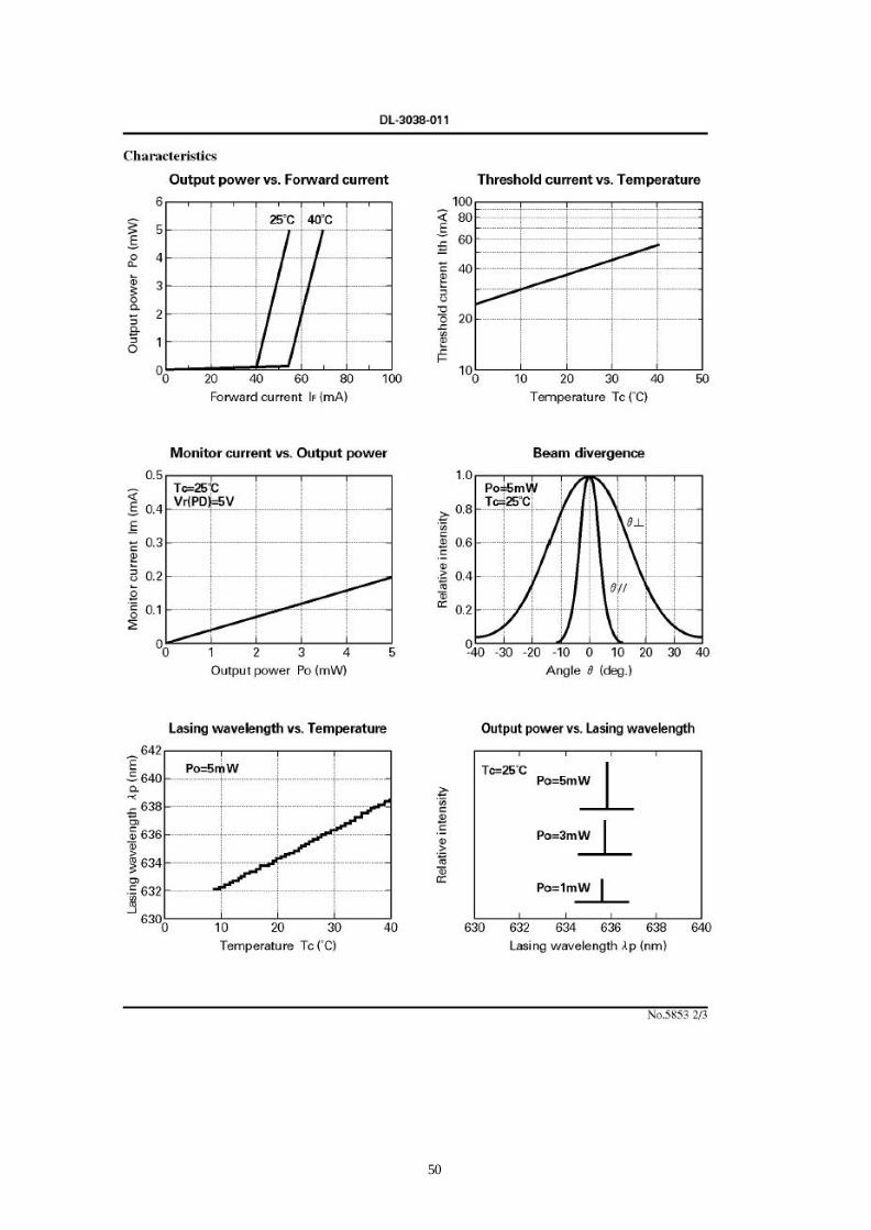
50
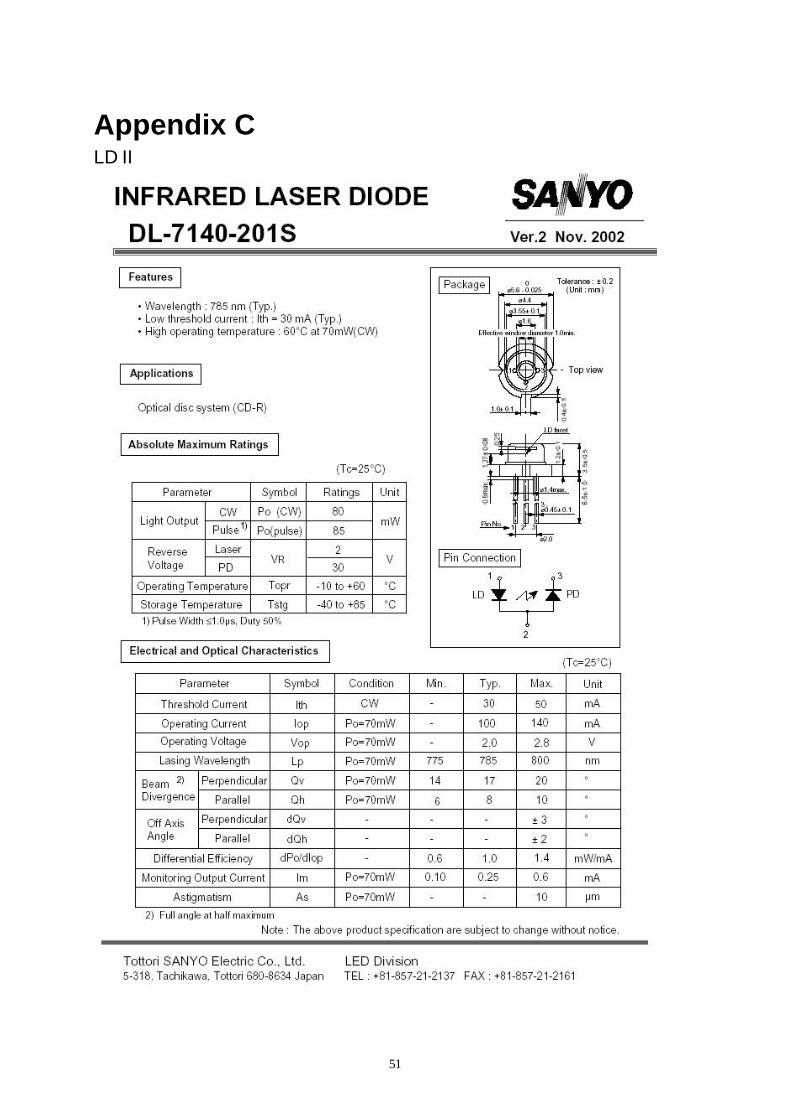
51
Appendix C LD II
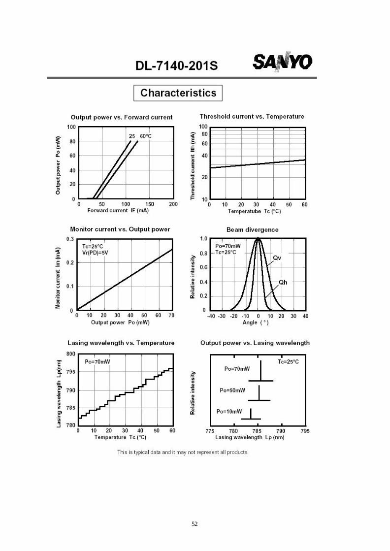
52
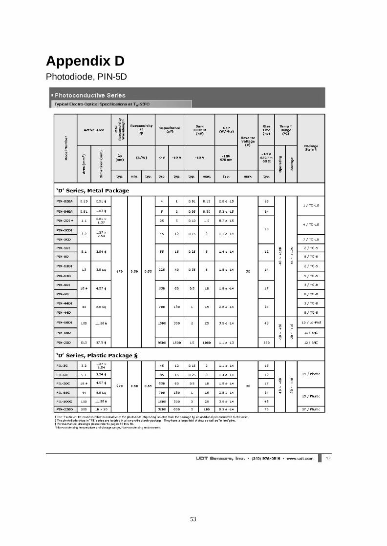
53
Appendix D Photodiode, PIN-5D