semiconductor detector systems - school of physicsdjpeake/spieler_semiconductor_det… · 1.3 pulse...
TRANSCRIPT

Semiconductor DetectorSystems
Helmuth SpielerPhysics Division, Lawrence Berkeley National Laboratory
1
3Great Clarendon Street, Oxford OX2 6DP
Oxford University Press is a department of the University of Oxford.
It furthers the University’s objective of excellence in research, scholarship,
and education by publishing worldwide in
Oxford New York
Auckland Cape Town Dar es Salaam Hong Kong Karachi
Kuala Lumpur Madrid Melbourne Mexico City Nairobi
New Delhi Shanghai Taipei Toronto
With offices in
Argentina Austria Brazil Chile Czech Republic France Greece
Guatemala Hungary Italy Japan Poland Portugal Singapore
South Korea Switzerland Thailand Turkey Ukraine Vietnam
Oxford is a registered trade mark of Oxford University Press
in the UK and in certain other countries
Published in the United States
by Oxford University Press Inc., New York
© Oxford University Press 2005
The moral rights of the author have been asserted
Database right Oxford University Press (maker)
First published 2005
All rights reserved. No part of this publication may be reproduced,
stored in a retrieval system, or transmitted, in any form or by any means,
without the prior permission in writing of Oxford University Press,
or as expressly permitted by law, or under terms agreed with the appropriate
reprographics rights organization. Enquiries concerning reproduction
outside the scope of the above should be sent to the Rights Department,
Oxford University Press, at the address above
You must not circulate this book in any other binding or cover
and you must impose this same condition on any acquirer
British Library Cataloguing in Publication Data
Data available
Library of Congress Cataloging in Publication Data
Data available
Typeset by
Printed in Great Britain
on acid-free paper by
Biddles Ltd., King’s Lynn
ISBN 0–19–852784–5 978–0–19–852784–8
1 3 5 7 9 10 8 6 4 2

ACKNOWLEDGEMENTS
This book is the result of countless interactions with friends, colleagues, and col-laborators too numerous to list individually. However, some bear more respon-sibility than others. Through persistant questioning over the past two decades,Bob Ely and Carl Haber prompted me to rethink and develop significant por-tions of the material presented here. Unfortunately, the responsibility for anymistakes or inaccuracies is mine.
At Lawrence Berkeley National Laboratory my work is supported by the Di-rector, Office of Science, Office of High Energy and Nuclear Physics, of the U.S.Department of Energy under Contract No. DE-AC03-76SF00098, but a project-driven environment with inadequate budgets is hardly conducive to probing be-yond what is absolutely necessary for detector design and construction. As aresult, the lengthy process of understanding the physics and technology of semi-conductor sensors and electronics, developing (and discarding) concepts, andfinally the preparation of this book were very much a night-time and weekendeffort. Foremost, I thank my wife Sigrid for wholeheartedly supporting this effortand understanding my faraway gazes at the breakfast and dinner table.
Helmuth Spieler
Pinole, CaliforniaJuly, 2005
viii
1
DETECTOR SYSTEMS OVERVIEW
All semiconductor detector systems include the same basic functions. The signalfrom each sensor or sensor channel in a detector array must be amplified andprocessed for storage and analysis. Some functions are clearly associated withindividual circuit blocks, but frequently circuit blocks perform multiple functions.
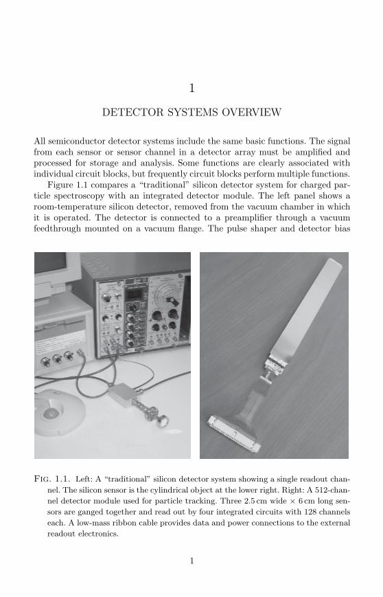
Figure 1.1 compares a “traditional” silicon detector system for charged par-ticle spectroscopy with an integrated detector module. The left panel shows aroom-temperature silicon detector, removed from the vacuum chamber in whichit is operated. The detector is connected to a preamplifier through a vacuumfeedthrough mounted on a vacuum flange. The pulse shaper and detector bias
Fig. 1.1. Left: A “traditional” silicon detector system showing a single readout chan-
nel. The silicon sensor is the cylindrical object at the lower right. Right: A 512-chan-
nel detector module used for particle tracking. Three 2.5 cm wide × 6 cm long sen-
sors are ganged together and read out by four integrated circuits with 128 channels
each. A low-mass ribbon cable provides data and power connections to the external
readout electronics.
1
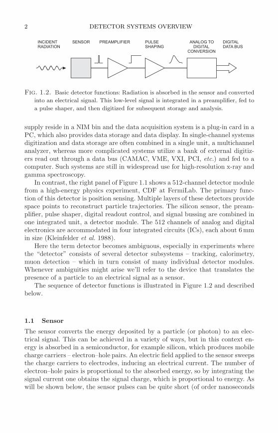
2 DETECTOR SYSTEMS OVERVIEW
INCIDENT
RADIATION
SENSOR PREAMPLIFIER PULSE
SHAPING
ANALOG TO
DIGITAL
CONVERSION
DIGITAL
DATA BUS
Fig. 1.2. Basic detector functions: Radiation is absorbed in the sensor and converted
into an electrical signal. This low-level signal is integrated in a preamplifier, fed to
a pulse shaper, and then digitized for subsequent storage and analysis.
supply reside in a NIM bin and the data acquisition system is a plug-in card in aPC, which also provides data storage and data display. In single-channel systemsdigitization and data storage are often combined in a single unit, a multichannelanalyzer, whereas more complicated systems utilize a bank of external digitiz-ers read out through a data bus (CAMAC, VME, VXI, PCI, etc.) and fed to acomputer. Such systems are still in widespread use for high-resolution x-ray andgamma spectroscopy.
In contrast, the right panel of Figure 1.1 shows a 512-channel detector modulefrom a high-energy physics experiment, CDF at FermiLab. The primary func-tion of this detector is position sensing. Multiple layers of these detectors providespace points to reconstruct particle trajectories. The silicon sensor, the pream-plifier, pulse shaper, digital readout control, and signal bussing are combined inone integrated unit, a detector module. The 512 channels of analog and digitalelectronics are accommodated in four integrated circuits (ICs), each about 6mmin size (Kleinfelder et al. 1988).
Here the term detector becomes ambiguous, especially in experiments wherethe “detector” consists of several detector subsystems – tracking, calorimetry,muon detection – which in turn consist of many individual detector modules.Whenever ambiguities might arise we’ll refer to the device that translates thepresence of a particle to an electrical signal as a sensor.
The sequence of detector functions is illustrated in Figure 1.2 and describedbelow.
1.1 Sensor
The sensor converts the energy deposited by a particle (or photon) to an elec-trical signal. This can be achieved in a variety of ways, but in this context en-ergy is absorbed in a semiconductor, for example silicon, which produces mobilecharge carriers – electron–hole pairs. An electric field applied to the sensor sweepsthe charge carriers to electrodes, inducing an electrical current. The number ofelectron–hole pairs is proportional to the absorbed energy, so by integrating thesignal current one obtains the signal charge, which is proportional to energy. Aswill be shown below, the sensor pulses can be quite short (of order nanoseconds
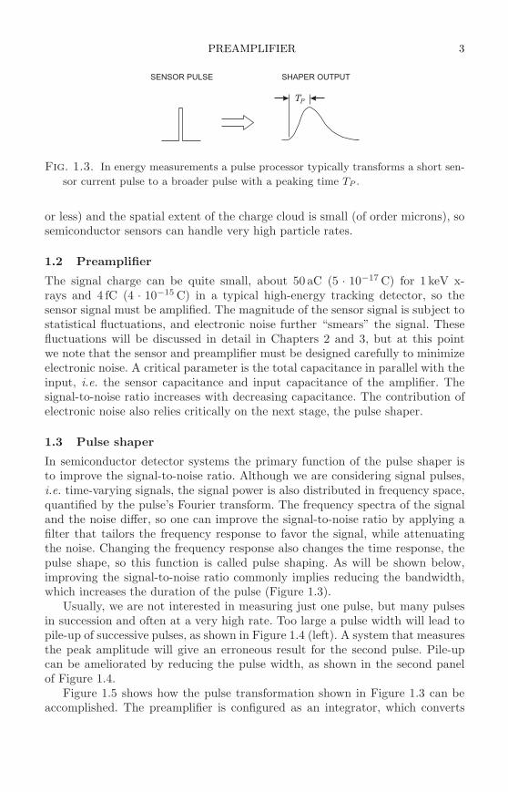
PREAMPLIFIER 3
TP
SENSOR PULSE SHAPER OUTPUT
Fig. 1.3. In energy measurements a pulse processor typically transforms a short sen-
sor current pulse to a broader pulse with a peaking time TP .
or less) and the spatial extent of the charge cloud is small (of order microns), sosemiconductor sensors can handle very high particle rates.
1.2 Preamplifier
The signal charge can be quite small, about 50 aC (5 · 10−17 C) for 1 keV x-rays and 4 fC (4 · 10−15 C) in a typical high-energy tracking detector, so thesensor signal must be amplified. The magnitude of the sensor signal is subject tostatistical fluctuations, and electronic noise further “smears” the signal. Thesefluctuations will be discussed in detail in Chapters 2 and 3, but at this pointwe note that the sensor and preamplifier must be designed carefully to minimizeelectronic noise. A critical parameter is the total capacitance in parallel with theinput, i.e. the sensor capacitance and input capacitance of the amplifier. Thesignal-to-noise ratio increases with decreasing capacitance. The contribution ofelectronic noise also relies critically on the next stage, the pulse shaper.
1.3 Pulse shaper
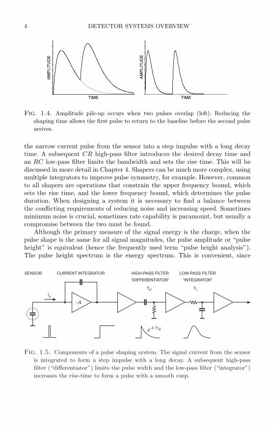
In semiconductor detector systems the primary function of the pulse shaper isto improve the signal-to-noise ratio. Although we are considering signal pulses,i.e. time-varying signals, the signal power is also distributed in frequency space,quantified by the pulse’s Fourier transform. The frequency spectra of the signaland the noise differ, so one can improve the signal-to-noise ratio by applying afilter that tailors the frequency response to favor the signal, while attenuatingthe noise. Changing the frequency response also changes the time response, thepulse shape, so this function is called pulse shaping. As will be shown below,improving the signal-to-noise ratio commonly implies reducing the bandwidth,which increases the duration of the pulse (Figure 1.3).
Usually, we are not interested in measuring just one pulse, but many pulsesin succession and often at a very high rate. Too large a pulse width will lead topile-up of successive pulses, as shown in Figure 1.4 (left). A system that measuresthe peak amplitude will give an erroneous result for the second pulse. Pile-upcan be ameliorated by reducing the pulse width, as shown in the second panelof Figure 1.4.
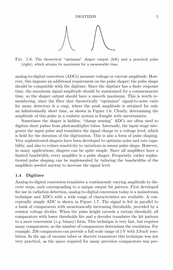
Figure 1.5 shows how the pulse transformation shown in Figure 1.3 can beaccomplished. The preamplifier is configured as an integrator, which converts
4 DETECTOR SYSTEMS OVERVIEW
TIME
AMPLITUDE
TIME
AMPLITUDE
Fig. 1.4. Amplitude pile-up occurs when two pulses overlap (left). Reducing the
shaping time allows the first pulse to return to the baseline before the second pulse
arrives.
the narrow current pulse from the sensor into a step impulse with a long decaytime. A subsequent CR high-pass filter introduces the desired decay time andan RC low-pass filter limits the bandwidth and sets the rise time. This will bediscussed in more detail in Chapter 4. Shapers can be much more complex, usingmultiple integrators to improve pulse symmetry, for example. However, commonto all shapers are operations that constrain the upper frequency bound, whichsets the rise time, and the lower frequency bound, which determines the pulseduration. When designing a system it is necessary to find a balance betweenthe conflicting requirements of reducing noise and increasing speed. Sometimesminimum noise is crucial, sometimes rate capability is paramount, but usually acompromise between the two must be found.
Although the primary measure of the signal energy is the charge, when thepulse shape is the same for all signal magnitudes, the pulse amplitude or “pulseheight” is equivalent (hence the frequently used term “pulse height analysis”).The pulse height spectrum is the energy spectrum. This is convenient, since
d i
HIGH-PASS FILTERCURRENT INTEGRATOR
“DIFFERENTIATOR” “INTEGRATOR”
LOW-PASS FILTER
e-t /d
is
A
SENSOR
Fig. 1.5. Components of a pulse shaping system. The signal current from the sensor
is integrated to form a step impulse with a long decay. A subsequent high-pass
filter (“differentiator”) limits the pulse width and the low-pass filter (“integrator”)
increases the rise-time to form a pulse with a smooth cusp.
DIGITIZER 5
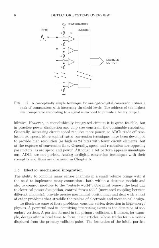
Fig. 1.6. The theoretical “optimum” shaper output (left) and a practical pulse
(right), which attains its maximum for a measurable time.
analog-to-digital converters (ADCs) measure voltage or current amplitude. How-ever, this imposes an additional requirement on the pulse shaper; the pulse shapeshould be compatible with the digitizer. Since the digitizer has a finite responsetime, the maximum signal amplitude should be maintained for a commensuratetime, so the shaper output should have a smooth maximum. This is worth re-membering, since the filter that theoretically “optimizes” signal-to-noise ratiofor many detectors is a cusp, where the peak amplitude is attained for onlyan infinitesimally short time, as shown in Figure 1.6. Clearly, determining theamplitude of this pulse in a realistic system is fraught with uncertainties.
Sometimes the shaper is hidden; “charge sensing” ADCs are often used todigitize short pulses from photomultiplier tubes. Internally, the input stage inte-grates the input pulse and translates the signal charge to a voltage level, whichis held for the duration of the digitization. This is also a form of pulse shaping.Very sophisticated shapers have been developed to optimize noise and rate capa-bility, and also to reduce sensitivity to variations in sensor pulse shape. However,in many applications, shapers can be quite simple. Since all amplifiers have alimited bandwidth, every amplifier is a pulse shaper. Frequently, rather sophis-ticated pulse shaping can be implemented by tailoring the bandwidths of theamplifiers needed anyway to increase the signal level.
1.4 Digitizer
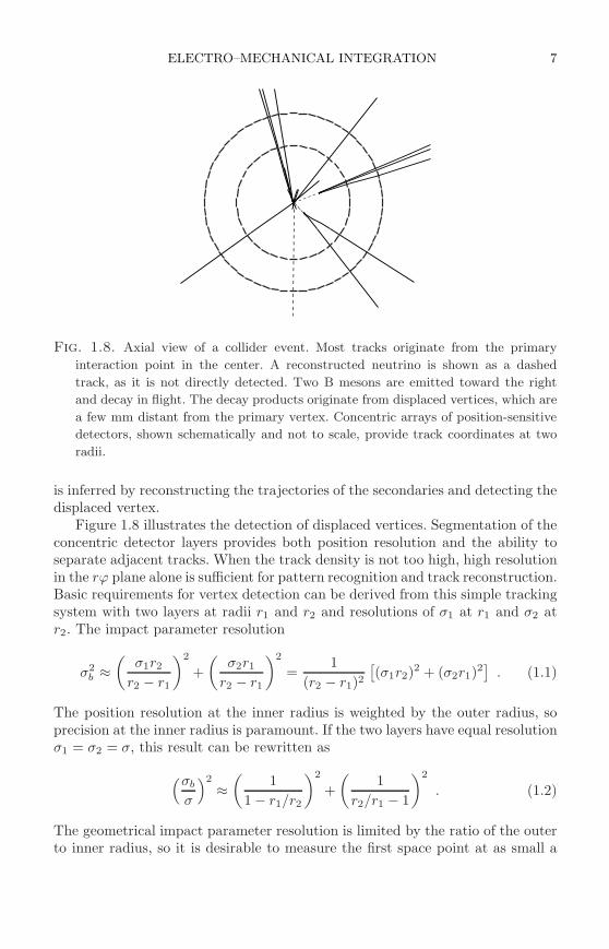
Analog-to-digital conversion translates a continuously varying amplitude to dis-crete steps, each corresponding to a unique output bit pattern. First developedfor use in radiation detection, analog-to-digital conversion today is a mainstreamtechnique and ADCs with a wide range of characteristics are available. A con-ceptually simple ADC is shown in Figure 1.7. The signal is fed in parallel toa bank of comparators with monotonically increasing thresholds, provided by aresistor voltage divider. When the pulse height exceeds a certain threshold, allcomparators with lower thresholds fire and a decoder translates the hit patternto a more convenient (e.g. binary) form. This technique is very fast, but requiresmany comparators, as the number of comparators determines the resolution. Forexample, 256 comparators can provide a full scale range of 1 V with 3.9mV reso-lution. In the age of vacuum tubes or discrete transistors this technique was notvery practical, as the space required for many precision comparators was pro-
6 DETECTOR SYSTEMS OVERVIEW
Vref
R
R
R
R
R
DIGITIZED
OUTPUT
COMPARATORS
ENCODERINPUT
Fig. 1.7. A conceptually simple technique for analog-to-digital conversion utilizes a
bank of comparators with increasing threshold levels. The address of the highest
level comparator responding to a signal is encoded to provide a binary output.
hibitive. However, in monolithically integrated circuits it is quite feasible, butin practice power dissipation and chip size constrain the obtainable resolution.Generally, increasing circuit speed requires more power, so ADCs trade off reso-lution vs. speed. More sophisticated conversion techniques have been developedto provide high resolution (as high as 24 bits) with fewer circuit elements, butat the expense of conversion time. Generally, speed and resolution are opposingparameters, as are speed and power. Although a bit pattern appears unambigu-ous, ADCs are not perfect. Analog-to-digital conversion techniques with theirstrengths and flaws are discussed in Chapter 5.
1.5 Electro–mechanical integration
The ability to combine many sensor channels in a small volume brings with itthe need to implement many connections, both within a detector module andalso to connect modules to the “outside world”. One must remove the heat dueto electrical power dissipation, control “cross-talk” (unwanted coupling betweendifferent channels), provide precise mechanical positioning, and deal with a hostof other problems that straddle the realms of electronic and mechanical design.
To illustrate some of these problems, consider vertex detection in high-energyphysics. A powerful tool in identifying interesting events is the detection of sec-ondary vertices. A particle formed in the primary collision, a B meson, for exam-ple, decays after a brief time to form new particles, whose tracks form a vertexdisplaced from the primary collision point. The formation of the initial particle
ELECTRO–MECHANICAL INTEGRATION 7
Fig. 1.8. Axial view of a collider event. Most tracks originate from the primary
interaction point in the center. A reconstructed neutrino is shown as a dashed
track, as it is not directly detected. Two B mesons are emitted toward the right
and decay in flight. The decay products originate from displaced vertices, which are
a few mm distant from the primary vertex. Concentric arrays of position-sensitive
detectors, shown schematically and not to scale, provide track coordinates at two
radii.
is inferred by reconstructing the trajectories of the secondaries and detecting thedisplaced vertex.
Figure 1.8 illustrates the detection of displaced vertices. Segmentation of theconcentric detector layers provides both position resolution and the ability toseparate adjacent tracks. When the track density is not too high, high resolutionin the rϕ plane alone is sufficient for pattern recognition and track reconstruction.Basic requirements for vertex detection can be derived from this simple trackingsystem with two layers at radii r1 and r2 and resolutions of σ1 at r1 and σ2 atr2. The impact parameter resolution
σ2b ≈
(
σ1r2
r2 − r1
)2
+
(
σ2r1
r2 − r1
)2
=1
(r2 − r1)2[
(σ1r2)2 + (σ2r1)
2]
. (1.1)
The position resolution at the inner radius is weighted by the outer radius, soprecision at the inner radius is paramount. If the two layers have equal resolutionσ1 = σ2 = σ, this result can be rewritten as
(σb
σ
)2
≈(
1
1 − r1/r2
)2
+
(
1
r2/r1 − 1
)2
. (1.2)
The geometrical impact parameter resolution is limited by the ratio of the outerto inner radius, so it is desirable to measure the first space point at as small a
8 DETECTOR SYSTEMS OVERVIEW
radius as possible. The obtainable impact parameter resolution improves rapidlyfrom σb/σ = 7.8 at r2/r1 = 1.2 to σb/σ = 2.2 at r2/r1 = 2 and attains values <1.3 at r2/r1 > 5. For σ = 10 µm and r2/r1 = 2, σb ≈ 20µm. Thus, the inner layerrequires a high-resolution detector, which also implies a high-density electronicreadout with associated cabling and cooling, mounted on a precision supportstructure. All of this adds material, which imposes an additional constraint.
The obtainable vertex resolution is affected by angular deflection due to mul-tiple scattering from material in the detector volume. The scattering angle
Θrms =0.0136[GeV/c]
p⊥
√
x
X0
[
1 + 0.038 · ln(
x
X0
)]
, (1.3)
where p⊥ is the particle momentum, x the thickness of the material, and X0
the radiation length (see Particle Data Group 2004 for a concise summary). Asnoted above, the position resolution at inner radii is critical, so it is important tominimize material close to the interaction. Typically, the first layer of materialis the beam pipe.
Consider a Be beam pipe of x = 1 mm thickness and R = 5cm radius. Theradiation length of Be is X0 = 35.3 cm, so x/X0 = 2.8·10−3 and at p⊥ = 1GeV/cthe scattering angle Θrms = 0.56mrad. This corresponds to σbΘrms = 28 µm,which in this example would dominate the obtainable resolution. Clearly, anymaterial between the interaction and the measurement point should be mini-mized and the first measurement should be at as small a radius as possible. Thisexercise shows how experimental requirements drive the first detector layers tosmall radii, which increases the particle flux (hits per unit area) and radiationdamage.
The need to reduce material imposes severe constraints on the sensor andelectronics, the support structures, and the power dissipation, which determinesthe material in the cooling systems and power cabling. Since large-scale arrayscombine both analog and digital functions in the detector module, special tech-niques must be applied to reduce pickup from digital switching without utilizingmassive shielding. Similar constraints apply in other applications, x-ray imagers,for example, where Compton scattering blurs the image.
Subsequent chapters will provide detailed discussions of the relevant physicsand design parameters. In the spirit of a “road map” the remainder of thischapter summarizes the key aspects of semiconductor detector systems.
1.6 Sensor structures I
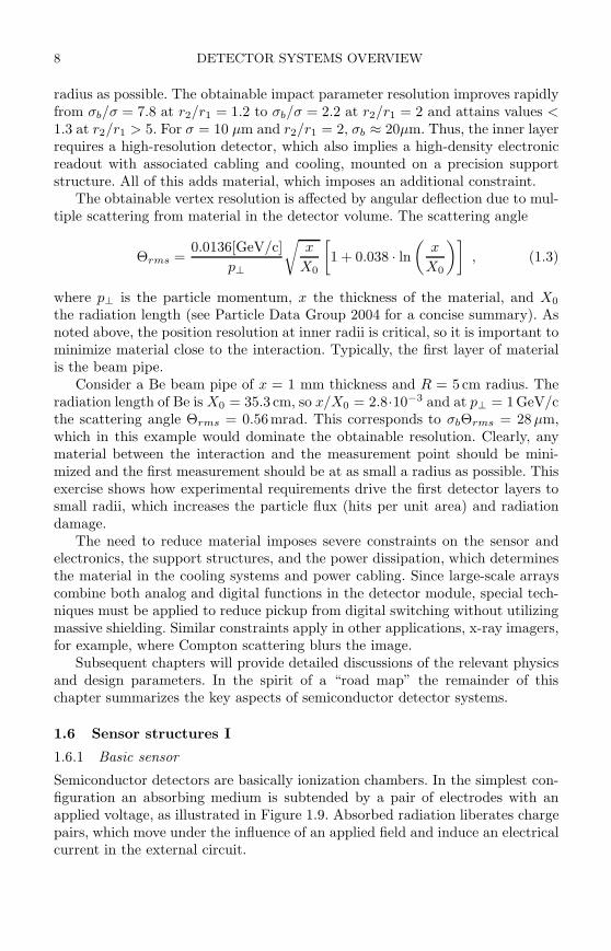
1.6.1 Basic sensor
Semiconductor detectors are basically ionization chambers. In the simplest con-figuration an absorbing medium is subtended by a pair of electrodes with anapplied voltage, as illustrated in Figure 1.9. Absorbed radiation liberates chargepairs, which move under the influence of an applied field and induce an electricalcurrent in the external circuit.
SENSOR STRUCTURES I 9
Vbias
i
i
sig
sig
Fig. 1.9. Charge collection in a simple ionization chamber.
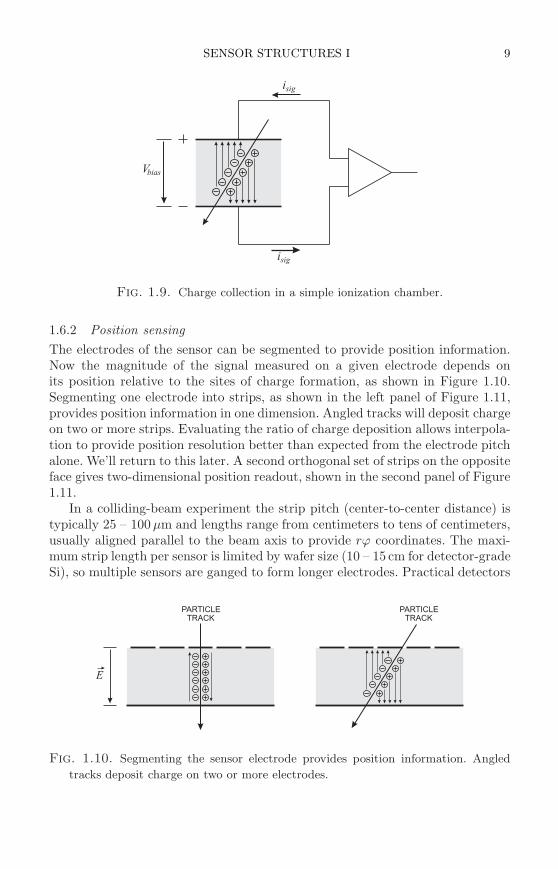
1.6.2 Position sensing
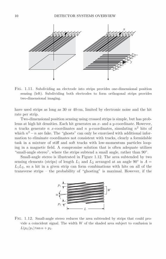
The electrodes of the sensor can be segmented to provide position information.Now the magnitude of the signal measured on a given electrode depends onits position relative to the sites of charge formation, as shown in Figure 1.10.Segmenting one electrode into strips, as shown in the left panel of Figure 1.11,provides position information in one dimension. Angled tracks will deposit chargeon two or more strips. Evaluating the ratio of charge deposition allows interpola-tion to provide position resolution better than expected from the electrode pitchalone. We’ll return to this later. A second orthogonal set of strips on the oppositeface gives two-dimensional position readout, shown in the second panel of Figure1.11.
In a colliding-beam experiment the strip pitch (center-to-center distance) istypically 25 – 100 µm and lengths range from centimeters to tens of centimeters,usually aligned parallel to the beam axis to provide rϕ coordinates. The maxi-mum strip length per sensor is limited by wafer size (10 – 15 cm for detector-gradeSi), so multiple sensors are ganged to form longer electrodes. Practical detectors
PARTICLE
TRACK
E
PARTICLE
TRACK
Fig. 1.10. Segmenting the sensor electrode provides position information. Angled
tracks deposit charge on two or more electrodes.
10 DETECTOR SYSTEMS OVERVIEW
y
x
Fig. 1.11. Subdividing an electrode into strips provides one-dimensional position
sensing (left). Subdividing both electrodes to form orthogonal strips provides
two-dimensional imaging.
have used strips as long as 30 or 40 cm, limited by electronic noise and the hitrate per strip.
Two-dimensional position sensing using crossed strips is simple, but has prob-lems at high hit densities. Each hit generates an x- and a y-coordinate. However,n tracks generate n x-coordinates and n y-coordinates, simulating n2 hits ofwhich n2 −n are fake. The “ghosts” can only be exorcised with additional infor-mation to eliminate coordinates not consistent with tracks, clearly a formidabletask in a mixture of stiff and soft tracks with low-momentum particles loop-ing in a magnetic field. A compromise solution that is often adequate utilizes“small-angle stereo”, where the strips subtend a small angle, rather than 90.
Small-angle stereo is illustrated in Figure 1.12. The area subtended by twosensing elements (strips) of length L1 and L2 arranged at an angle 90 is A =L1L2, so a hit in a given strip can form combinations with hits on all of thetransverse strips – the probability of “ghosting” is maximal. However, if the
L
p1
p2
W
Fig. 1.12. Small-angle stereo reduces the area subtended by strips that could pro-
vide a coincident signal. The width W of the shaded area subject to confusion is
L(p2/p1) tanα + p2.
SENSOR STRUCTURES I 11
angle α subtended by the two strip arrays is small (and their lengths L areapproximately equal), the capture area
A ≈ L2 p2
p1tan α + Lp2 . (1.4)
Consider a given horizontal strip struck by a particle. To determine the longitu-dinal coordinate, all angled strips that cross the primary strip must be checkedand every hit that deposits charge on these strips adds a coordinate that mustbe considered in conjunction with the coordinate defined by the horizontal strip.Since each strip captures charge from a width equal to the strip pitch, the exactwidth of the capture area is an integer multiple of the strip pitch. The probabilityof multiple hits within the acceptance area, and hence the number of “ghosts”, isreduced as α is made smaller, but at the expense of resolution in the longitudinalcoordinate.
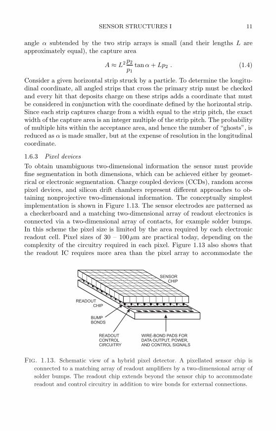
1.6.3 Pixel devices
To obtain unambiguous two-dimensional information the sensor must providefine segmentation in both dimensions, which can be achieved either by geomet-rical or electronic segmentation. Charge coupled devices (CCDs), random accesspixel devices, and silicon drift chambers represent different approaches to ob-taining nonprojective two-dimensional information. The conceptually simplestimplementation is shown in Figure 1.13. The sensor electrodes are patterned asa checkerboard and a matching two-dimensional array of readout electronics isconnected via a two-dimensional array of contacts, for example solder bumps.In this scheme the pixel size is limited by the area required by each electronicreadout cell. Pixel sizes of 30 – 100µm are practical today, depending on thecomplexity of the circuitry required in each pixel. Figure 1.13 also shows thatthe readout IC requires more area than the pixel array to accommodate the
READOUT
CHIP
SENSOR
CHIP
BUMP
BONDS
READOUT
CONTROL
CIRCUITRY
WIRE-BOND PADS FOR
DATA OUTPUT, POWER,
AND CONTROL SIGNALS
Fig. 1.13. Schematic view of a hybrid pixel detector. A pixellated sensor chip is
connected to a matching array of readout amplifiers by a two-dimensional array of
solder bumps. The readout chip extends beyond the sensor chip to accommodate
readout and control circuitry in addition to wire bonds for external connections.
12 DETECTOR SYSTEMS OVERVIEW
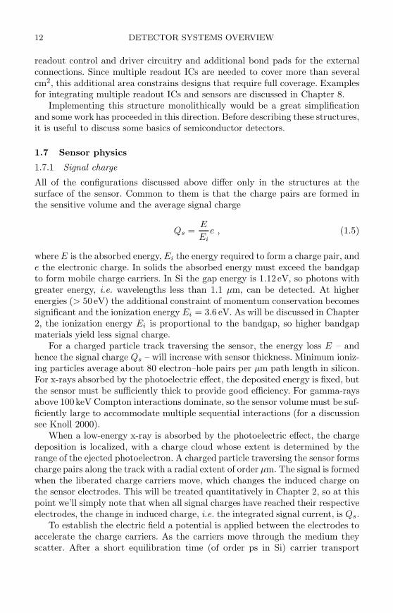
readout control and driver circuitry and additional bond pads for the externalconnections. Since multiple readout ICs are needed to cover more than severalcm2, this additional area constrains designs that require full coverage. Examplesfor integrating multiple readout ICs and sensors are discussed in Chapter 8.
Implementing this structure monolithically would be a great simplificationand some work has proceeded in this direction. Before describing these structures,it is useful to discuss some basics of semiconductor detectors.
1.7 Sensor physics
1.7.1 Signal charge
All of the configurations discussed above differ only in the structures at thesurface of the sensor. Common to them is that the charge pairs are formed inthe sensitive volume and the average signal charge
Qs =E
Eie , (1.5)
where E is the absorbed energy, Ei the energy required to form a charge pair, ande the electronic charge. In solids the absorbed energy must exceed the bandgapto form mobile charge carriers. In Si the gap energy is 1.12 eV, so photons withgreater energy, i.e. wavelengths less than 1.1 µm, can be detected. At higherenergies (> 50 eV) the additional constraint of momentum conservation becomessignificant and the ionization energy Ei = 3.6 eV. As will be discussed in Chapter2, the ionization energy Ei is proportional to the bandgap, so higher bandgapmaterials yield less signal charge.
For a charged particle track traversing the sensor, the energy loss E – andhence the signal charge Qs – will increase with sensor thickness. Minimum ioniz-ing particles average about 80 electron–hole pairs per µm path length in silicon.For x-rays absorbed by the photoelectric effect, the deposited energy is fixed, butthe sensor must be sufficiently thick to provide good efficiency. For gamma-raysabove 100keV Compton interactions dominate, so the sensor volume must be suf-ficiently large to accommodate multiple sequential interactions (for a discussionsee Knoll 2000).
When a low-energy x-ray is absorbed by the photoelectric effect, the chargedeposition is localized, with a charge cloud whose extent is determined by therange of the ejected photoelectron. A charged particle traversing the sensor formscharge pairs along the track with a radial extent of order µm. The signal is formedwhen the liberated charge carriers move, which changes the induced charge onthe sensor electrodes. This will be treated quantitatively in Chapter 2, so at thispoint we’ll simply note that when all signal charges have reached their respectiveelectrodes, the change in induced charge, i.e. the integrated signal current, is Qs.
To establish the electric field a potential is applied between the electrodes toaccelerate the charge carriers. As the carriers move through the medium theyscatter. After a short equilibration time (of order ps in Si) carrier transport
SENSOR PHYSICS 13
becomes nonballistic and the velocity does not depend on the duration of ac-celeration, but only on the magnitude of the local electric field (see Sze 1981).Thus, the velocity of carriers at position x depends only on the local electric fieldE(x), regardless of where they originated and how long they have moved. Thecarrier velocity
v(x) = µE(x) , (1.6)
where µ is the mobility. For example, in Si the mobility is 1350 V/cm · s2 forelectrons and 450 V/cm · s2 for holes. As an estimate to set the scale, applying30V across a 300 µm thick absorber yields an average field of 103 V/cm, so thevelocity of electrons is about 1.4 · 106 cm/s and it will take about 20ns for anelectron to traverse the detector thickness. A hole takes three times as long.
1.7.2 Sensor volume
To establish a high field with a small quiescent current, the conductivity of theabsorber must be low. Signal currents are typically of order µA, so if in the aboveexample the quiescent current is to be small compared to the signal current, theresistance between the electrodes should be ≫ 30MΩ. In an ideal solid the re-sistivity depends exponentially on the bandgap. Increasing the bandgap reducesthe signal charge, so the range of suitable materials is limited. Diamond is anexcellent insulator, but the ionization energy Ei is about 6 eV and the range ofavailable thickness is limited. In semiconductors the ionization energy is smaller,2.9 eV in Ge and 3.6 eV in Si. Si material can be grown with resistivities of order104 Ω cm, which is too low; a 300 µm thick sensor with 1 cm2 area would have aresistance of 300 Ω, so 30V would lead to a current flow of 100mA and a powerdissipation of 3W. On the other hand, high-quality single crystals of Si and Gecan be grown economically with suitably large volumes, so to mitigate the effectof resistivity one resorts to reverse-biased diode structures.
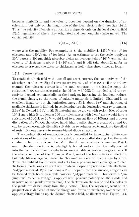
The conductivity of semiconductors is controlled by introducing dilute con-centrations of impurities into the crystal, a process called doping. Let the semi-conductor be of atomic number Z. If the dopant is of atomic number Z + 1,one of the shell electrons is only lightly bound and can be thermally excitedinto the conduction band, so electrons are available as mobile charge carriers. Ifthe atomic number of the dopant is Z − 1, one of the bonds lacks an electron,but only little energy is needed to “borrow” an electron from a nearby atom.Thus, the unfilled bond moves and acts like a positive mobile charge, a “hole”.To form a diode, one can start with material doped to provide mobile electrons,“n-type” material. By introducing a Z −1 dopant from the surface, a region canbe formed with holes as mobile carriers, “p-type” material. This forms a “pn-junction”. When a voltage is applied with positive polarity on the n-side andnegative on the p-side (reverse bias), the electrons on the n-side and the holes onthe p-side are drawn away from the junction. Thus, the region adjacent to thepn-junction is depleted of mobile charge and forms an insulator, over which theapplied voltage builds up the desired electric field, as illustrated in Figure 1.14.
14 DETECTOR SYSTEMS OVERVIEW
p n
V
Fig. 1.14. Adjoining regions of p- and n-type doping form a pn-junction (top). The
charge of the mobile electrons and holes (circled) is balanced by the charge of the
atomic cores, so charge neutrality is maintained. When an external potential is
applied with positive polarity on the n-side and negative polarity on the p-side
(bottom), the mobile charges are drawn away from the junction. This leaves a net
space charge from the atomic cores, which builds up a linear electric field in the
junction. This is treated analytically in Chapter 2.
Note that even in the absence of an externally applied voltage, thermal diffu-sion forms a depletion region. As electrons and holes diffuse from their originalhost atoms, a space charge region is formed and the resulting field limits theextent of thermal diffusion. As a result, every pn-junction starts off with a non-zero depletion width and a potential difference between the p- and n-sides, the“built-in” potential Vbi.
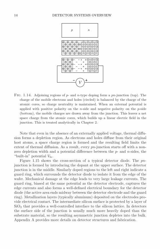
Figure 1.15 shows the cross-section of a typical detector diode. The pn-junction is formed by introducing the dopant at the upper surface. The detectorjunction is in the middle. Similarly doped regions to the left and right indicate aguard ring, which surrounds the detector diode to isolate it from the edge of thewafer. Mechanical damage at the edge leads to very large leakage currents. Theguard ring, biased at the same potential as the detector electrode, captures theedge currents and also forms a well-defined electrical boundary for the detectordiode (the active area ends midway between the detector electrode and the guardring). Metallization layers (typically aluminum) deposited on the electrodes pro-vide electrical contact. The intermediate silicon surface is protected by a layer ofSiO2 that provides a well-controlled interface to the silicon lattice. In detectorsthe surface side of the junction is usually much more heavily doped than thesubstrate material, so the resulting asymmetric junction depletes into the bulk.Appendix A provides more details on detector structures and fabrication.
SENSOR PHYSICS 15
300 m
~ 1 m
~ 1 m
GUARD RING
OHMIC CONTACT
JUNCTION CONTACTOXIDE
n BULK p DOPING+
Fig. 1.15. Detector diodes are usually asymmetric, with a highly doped layer at the
surface and a lightly doped bulk. With reverse bias the junction depletes into the
bulk. SiO2 layers protect the silicon surface and a guard ring isolates the diode from
the edges of the chip.
A reverse bias voltage Vb yields the depletion width
wd =
√
2ε(Vb + Vbi)
Ne, (1.7)
where N is the dopant concentration in the bulk and ε the dielectric constant(11.9ε0 for Si). The “built-in” junction potential Vbi in detector diodes is typicallyabout 0.5V. When the depletion width is less then the silicon thickness, the diodeis “partially depleted”. When wd extends to the back contact the diode is “fullydepleted”.
The depleted junction volume is free of mobile charge and thus forms a ca-pacitor, bounded by the conducting p- and n-type semiconductor on each side.The capacitance
C = εA
wd= A
√
εeN
2(Vb + Vbi). (1.8)
For bias voltages Vb ≫ Vbi
C ∝ 1√Vb
. (1.9)
In technical unitsC
A=
ε
wd≈ 1
[
pF
cm
]
1
W. (1.10)
A Si diode with 100 µm thickness has a capacitance of about 1 pF/mm2. This ap-plies to a detector whose electrodes are large compared to the depletion thickness.In strip and pixel detectors the fringing capacitance to neighboring electrodesusually dominates. The interstrip capacitance depends on the ratio of electrode
16 DETECTOR SYSTEMS OVERVIEW
width w to strip pitch p. For typical geometries the interstrip capacitance Cs percm length l follows the relationship (Demaria et al. 2000)
Cs
l=
(
0.03 + 1.62w + 20µm
p
)[
pF
cm
]
. (1.11)
Typically, the interstrip capacitance is about 1 pF/cm. The backplane capaci-tance
Cb ≈ εε0pl
w. (1.12)
Since the adjacent strips confine the fringing field lines to the interstrip bound-aries, the strip appears as an electrode with a width equal to the strip pitch.Corrections apply at large strip widths (Barberis et al. 1994).
Ideally, reverse bias removes all mobile carriers from the junction volume, sono current can flow. However, thermal excitation can promote electrons acrossthe bandgap, so a current flows even in the absence of radiation, hence theterm “dark current”. The probability of electrons surmounting the bandgap isincreased strongly by the presence of impurities in the lattice, as they introduceintermediate energy states in the gap that serve as “stepping stones”. As derivedin Appendix F the reverse bias current depends exponentially on temperatureT ,
IR ∝ T 2 exp
(
− Eg
2kT
)
, (1.13)
where Eg is the bandgap energy and k the Boltzmann constant, so cooling thedetector can reduce leakage substantially. The ratio of leakage currents at tem-peratures T1 and T2
IR(T2)
IR(T1)=
(
T2
T1
)2
exp
[
−Eg
2k
(
T1 − T2
T1T2
)]
. (1.14)
In Si (Eg =1.12 eV) this yields a ten-fold reduction in leakage current when thetemperature is lowered by 14 C from room temperature.
1.7.3 Charge collection
How quickly electrons and holes are swept from the depletion region is deter-mined by the electric field. To simplify the following equations we’ll set V ≡Vb + Vbi. At low reverse bias the field in the depletion region initially has atriangular profile
|E(x)| =eN
ε(wd − x) =
√
2Ne
εV ·
(
1 − x
wd
)
≡ Emax ·(
1 − x
wd
)
(1.15)
up to the voltage where the depletion width wd equals the thickness of the bulkd, corresponding to the depletion voltage
SENSOR PHYSICS 17
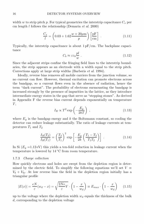
V< V V> Vd d
w d d
E
E
Emax
max
min
x x
E E
Fig. 1.16. Electric field distributions in a partially depleted detector (left) and a
detector operated with overbias (right).
Vd =Ned2
2ε. (1.16)
Increasing the bias voltage V beyond this point (“overbias”, often called “overde-pletion”) increases the field uniformly and evens out the field profile
|E(x)| =2Vd
d
(
1 − x
d
)
+V − Vd
d. (1.17)
Then the maximum field is (V + Vd)/d and the minimum field (V − Vd)/d.Figure 1.16 illustrates the electric field distributions in partial depletion andwith overbias.
When radiation forms electron–hole pairs, they drift under the influence ofthe field with a velocity v = µE. The time required for a carrier to traverse thefull detector thickness, the collection time, is
tc =d2
2µVlog
(
V + Vd + 2Vbi
V − Vd
)
, (1.18)
where the collection time for electrons or holes is obtained by using the appro-priate mobility. At full depletion or beyond, the collection time can be estimatedby using the average field E = V/d, so
tc ≈ d
v=
d
µE=
d2
µV(1.19)
and charge collection can be sped up by increasing the bias voltage. In partialdepletion, however, the collection time is independent of bias voltage and de-termined by the doping concentration alone, as d2/V remains constant. This isdiscussed in Chapter 2.
18 DETECTOR SYSTEMS OVERVIEW
In practice the dopant concentration N of silicon wafers is expressed as theresistivity of the material ρ = (eµN)−1, as this is readily measurable. Using thisparameter and introducing technical units yields the depletion voltage
Vdn = 4
[
Ω · cm(µm)2
]
· d2
ρn− Vbi (1.20)
for n-type material and
Vdp = 11
[
Ω · cm(µm)2
]
· d2
ρp− Vbi (1.21)
for p-type material. The resistivity of silicon suitable for tracking detectors (ormore precisely, the highest resistivity available economically) is 5 – 10 kΩ cm.Note that in 10 kΩ cm n-type Si the built-in voltage by itself depletes 45µmof material. Detector wafers are typically 300µm thick. Hence, the depletionvoltage in n-type material is 35 – 70V for the resistivity range given above.Assuming 6 kΩcm material (Vd = 60V) and an operating voltage of 90V, thecollection times for electrons and holes are 8 ns and 27ns, respectively. Electroncollection times tend to be somewhat longer then given by eqn 1.15 since theelectron mobility decreases at fields > 103 V/cm (see Chapter 2 and Sze 1981)and eventually the drift velocity saturates at 107 cm/s. At saturation velocity thecollection time is 10ps/µm. In partial depletion, as noted above, the collectiontime is independent of voltage and depends on resistivity alone. For electronsthe collection time constant
τcn = ρε = 1.05[ ns
k Ω · cm]
· ρ . (1.22)
To increase the depletion width or speed up the charge collection one canincrease the voltage, but ultimately this is limited by the onset of avalanching.At sufficiently high fields (greater than about 105 V/cm in Si) electrons acquireenough energy between collisions that secondary electrons are ejected. At evenhigher fields holes can eject secondary electrons, which in turn can eject newsecondaries, and a self-sustaining charge avalanche forms (see Chapter 2). Thisphenomenon is called “breakdown” and can cause permanent damage to the sen-sor. In practice avalanching often occurs at voltages much lower than predictedby eqn 1.17, since high fields can build up at the relatively sharp edges of thedoping distribution or electrode structures. When controlled, charge avalanchingcan be used to increase the signal charge, as discussed in Chapter 2. In detect-ing visible light, the primary signal charge is quite small, so this technique ismost often applied in photodiodes to provide internal gain and bring the signalabove the electronic noise level (avalanche photodiodes or APDs). APDs mustbe designed carefully to prevent breakdown and also to reduce additional signalfluctuations introduced by the avalanche process. Bias voltage and temperatureboth affect the gain strongly, so they must be kept stable.
SENSOR PHYSICS 19
1.7.4 Energy resolution
The minimum detectable signal and the precision of the amplitude measurementare limited by fluctuations. The signal formed in the sensor fluctuates, even for afixed energy absorption. Generally, sensors convert absorbed energy into signalquanta. In a scintillation detector absorbed energy is converted into a number ofscintillation photons. In an ionization chamber energy is converted into a numberof charge pairs (electrons and ions in gases or electrons and holes in solids). Theabsorbed energy divided by the excitation energy yields the average number ofsignal quanta
N =E
Ei. (1.23)
This number fluctuates statistically, so the relative resolution
∆E
E=
∆N
N=
√FN
N=
√
FEi
E. (1.24)
The resolution improves with the square root of energy. F is the Fano factor,which comes about because multiple excitation mechanisms can come into playand reduce the overall statistical spread. For example, in a semiconductor ab-sorbed energy forms electron–hole pairs, but also excites lattice vibrations –quantized as phonons – whose excitation energy is much smaller (meV vs. eV).Thus, many more excitations are involved than apparent from the charge sig-nal alone and this reduces the statistical fluctuations of the charge signal. Forexample, in Si the Fano factor is 0.1. The Fano factor is explained in Chapter 2.
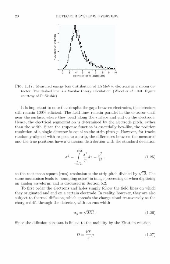
In most applications, the intrinsic energy resolution of semiconductor sensorsis so good that external contributions determine the overall fluctuations. How-ever, for low-energy x-rays signal charge fluctuations are significant, whereas ingamma-ray detectors electronic noise tends to determine the obtainable energyresolution. For minimum ionizing charged particles, it is the statistics of energyloss. Since the energy deposited by minimum ionizing particles varies accordingto a Landau–Vavilov distribution (Figure 1.17) with σQ/Qs ≈ 0.2 in 300 µmof Si, the inherent energy resolution of the detector is negligible. Nevertheless,electronic noise is still important in determining the minimum detectable signal,i.e. the detection efficiency.
1.7.5 Position resolution
The position resolution of the detector is determined to first order by the elec-trode geometry. The size and shape of the electrodes is limited by the size of awafer, on the one hand (10 or 15 cm diameter for detector grade material), andthe resolution capability of IC fabrication technology on the the other (∼ 1 µm).In practice the lower bound is set by the readout electronics, which in the small-est dimension tend to require 20 – 50 µm overall width. Most commonly, sensorsfor tracking applications have strip electrodes. The strips are usually 8 – 12µmwide, placed on a pitch of 25 – 50 µm, and 6 – 12 cm long. Frequently, multiplesensor wafers are ganged to form longer electrodes.
20 DETECTOR SYSTEMS OVERVIEW
32 4 5 6 7 8 9 10
DEPOSITED CHARGE (fC)
NU
MB
ER
OF
EV
EN
TS
Fig. 1.17. Measured energy loss distribution of 1.5 MeV/c electrons in a silicon de-
tector. The dashed line is a Vavilov theory calculation. (Wood et al. 1991. Figure
courtesy of P. Skubic)
It is important to note that despite the gaps between electrodes, the detectorsstill remain 100% efficient. The field lines remain parallel in the detector untilnear the surface, where they bend along the surface and end on the electrode.Hence, the electrical segmentation is determined by the electrode pitch, ratherthan the width. Since the response function is essentially box-like, the positionresolution of a single detector is equal to the strip pitch p. However, for tracksrandomly aligned with respect to a strip, the differences between the measuredand the true positions have a Gaussian distribution with the standard deviation
σ2 =
p/2∫
−p/2
x2
pdx =
p2
12, (1.25)
so the root mean square (rms) resolution is the strip pitch divided by√
12. Thesame mechanism leads to “sampling noise” in image processing or when digitizingan analog waveform, and is discussed in Section 5.2.
To first order the electrons and holes simply follow the field lines on whichthey originated and end on a certain electrode. In reality, however, they are alsosubject to thermal diffusion, which spreads the charge cloud transversely as thecharges drift through the detector, with an rms width
σy =√
2Dt . (1.26)
Since the diffusion constant is linked to the mobility by the Einstein relation
D =kT
eµ (1.27)
SENSOR PHYSICS 21
-15 -10 -5 5 10 15 [ m]
TRANSVERSE DIFFUSION
PARTICLE TRACK
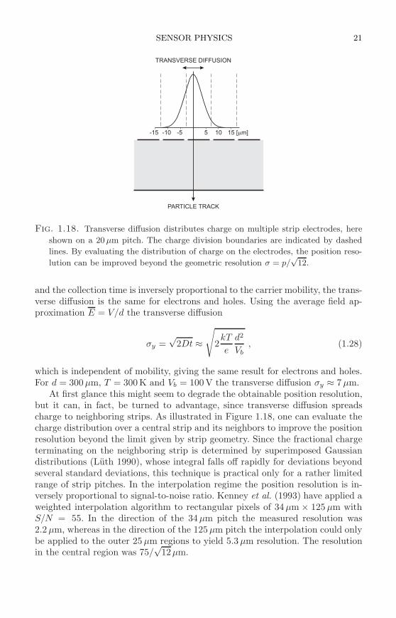
Fig. 1.18. Transverse diffusion distributes charge on multiple strip electrodes, here
shown on a 20 µm pitch. The charge division boundaries are indicated by dashed
lines. By evaluating the distribution of charge on the electrodes, the position reso-
lution can be improved beyond the geometric resolution σ = p/√
12.
and the collection time is inversely proportional to the carrier mobility, the trans-verse diffusion is the same for electrons and holes. Using the average field ap-proximation E = V/d the transverse diffusion
σy =√
2Dt ≈√
2kT
e
d2
Vb, (1.28)
which is independent of mobility, giving the same result for electrons and holes.For d = 300 µm, T = 300 K and Vb = 100 V the transverse diffusion σy ≈ 7 µm.
At first glance this might seem to degrade the obtainable position resolution,but it can, in fact, be turned to advantage, since transverse diffusion spreadscharge to neighboring strips. As illustrated in Figure 1.18, one can evaluate thecharge distribution over a central strip and its neighbors to improve the positionresolution beyond the limit given by strip geometry. Since the fractional chargeterminating on the neighboring strip is determined by superimposed Gaussiandistributions (Luth 1990), whose integral falls off rapidly for deviations beyondseveral standard deviations, this technique is practical only for a rather limitedrange of strip pitches. In the interpolation regime the position resolution is in-versely proportional to signal-to-noise ratio. Kenney et al. (1993) have applied aweighted interpolation algorithm to rectangular pixels of 34µm × 125 µm withS/N = 55. In the direction of the 34 µm pitch the measured resolution was2.2 µm, whereas in the direction of the 125 µm pitch the interpolation could onlybe applied to the outer 25 µm regions to yield 5.3 µm resolution. The resolutionin the central region was 75/
√12µm.
22 DETECTOR SYSTEMS OVERVIEW
PARTICLE
TRACK
E
-V
C C C C
CC C C
ss ss ss ss
bb b b
R R R R
Fig. 1.19. Intermediate “floating” electrodes can be used to reduce the effective read-
out pitch (left). The equivalent circuit (right) shows how the signal current induced
on the “floating” electrodes is transferred to the readout amplifiers through the
intermediate capacitive dividers formed by the strip-to-strip capacitance Css and
the backplane capacitance Cb.
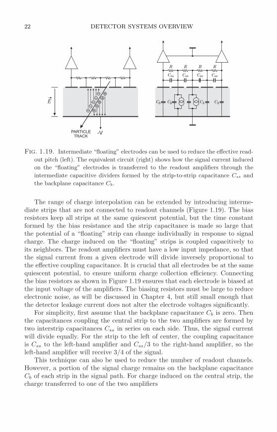
The range of charge interpolation can be extended by introducing interme-diate strips that are not connected to readout channels (Figure 1.19). The biasresistors keep all strips at the same quiescent potential, but the time constantformed by the bias resistance and the strip capacitance is made so large thatthe potential of a “floating” strip can change individually in response to signalcharge. The charge induced on the “floating” strips is coupled capacitively toits neighbors. The readout amplifiers must have a low input impedance, so thatthe signal current from a given electrode will divide inversely proportional tothe effective coupling capacitance. It is crucial that all electrodes be at the samequiescent potential, to ensure uniform charge collection efficiency. Connectingthe bias resistors as shown in Figure 1.19 ensures that each electrode is biased atthe input voltage of the amplifiers. The biasing resistors must be large to reduceelectronic noise, as will be discussed in Chapter 4, but still small enough thatthe detector leakage current does not alter the electrode voltages significantly.
For simplicity, first assume that the backplane capacitance Cb is zero. Thenthe capacitances coupling the central strip to the two amplifiers are formed bytwo interstrip capacitances Css in series on each side. Thus, the signal currentwill divide equally. For the strip to the left of center, the coupling capacitanceis Css to the left-hand amplifier and Css/3 to the right-hand amplifier, so theleft-hand amplifier will receive 3/4 of the signal.
This technique can also be used to reduce the number of readout channels.However, a portion of the signal charge remains on the backplane capacitanceCb of each strip in the signal path. For charge induced on the central strip, thecharge transferred to one of the two amplifiers
SENSOR PHYSICS 23
0.001 0.01 0.1 1 10 100 1000PHOTON ENERGY (MeV)
0.001
0.01
0.1
1
10
100
1000
10000
ABSORPTIO
NCOEFFICIENT(cm
-1)
RAYLEIGH
COMPTON
PHOTOELECTRIC
PAIR
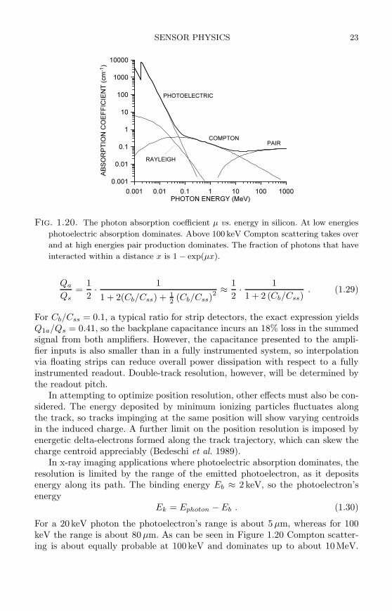
Fig. 1.20. The photon absorption coefficient µ vs. energy in silicon. At low energies
photoelectric absorption dominates. Above 100 keV Compton scattering takes over
and at high energies pair production dominates. The fraction of photons that have
interacted within a distance x is 1 − exp(µx).
Qa
Qs=
1
2· 1
1 + 2(Cb/Css) + 12 (Cb/Css)
2 ≈ 1
2· 1
1 + 2 (Cb/Css). (1.29)
For Cb/Css = 0.1, a typical ratio for strip detectors, the exact expression yieldsQ1a/Qs = 0.41, so the backplane capacitance incurs an 18% loss in the summedsignal from both amplifiers. However, the capacitance presented to the ampli-fier inputs is also smaller than in a fully instrumented system, so interpolationvia floating strips can reduce overall power dissipation with respect to a fullyinstrumented readout. Double-track resolution, however, will be determined bythe readout pitch.
In attempting to optimize position resolution, other effects must also be con-sidered. The energy deposited by minimum ionizing particles fluctuates alongthe track, so tracks impinging at the same position will show varying centroidsin the induced charge. A further limit on the position resolution is imposed byenergetic delta-electrons formed along the track trajectory, which can skew thecharge centroid appreciably (Bedeschi et al. 1989).
In x-ray imaging applications where photoelectric absorption dominates, theresolution is limited by the range of the emitted photoelectron, as it depositsenergy along its path. The binding energy Eb ≈ 2 keV, so the photoelectron’senergy
Ek = Ephoton − Eb . (1.30)
For a 20 keV photon the photoelectron’s range is about 5 µm, whereas for 100keV the range is about 80 µm. As can be seen in Figure 1.20 Compton scatter-ing is about equally probable at 100keV and dominates up to about 10MeV.
24 DETECTOR SYSTEMS OVERVIEW
However, given the maximum practical silicon detector thickness of several mmreasonable efficiency only obtains to 30 or 40 keV. Materials with higher atomicnumber are necessary for higher energies. Alternative materials are discussedbriefly in Chapter 2. At high energies pair production can be used to determinethe direction of gamma rays by detecting the emitted electrons and positrons ina silicon strip tracker (Chapter 8).
1.8 Sensor structures II – monolithic pixel devices
In the early years of large-scale semiconductor detectors the monolithic inte-gration of large scale sensors with electronics was viewed as the “holy grail”.Clearly, it is an appealing concept to have a 6 × 6 cm2 detector tile that com-bines a strip detector and 1200 channels of readout electronics with only thepower and data readout as external connections. The problem was perceived atthe time to be the incompatibility between IC and detector fabrication processes(see Appendix A). Development of an IC-compatible detector process allowedthe monolithic integration of high-quality electronics and full depletion siliconsensors without degrading sensor performance (Holland and Spieler 1990), subse-quently extended to full CMOS circuitry (Holland 1992). Nevertheless, a simpleyield estimate shows that this isn’t practical. In the conventional scheme read-ing out ∼ 1200 channels with a 50 µm readout pitch requires 10 ICs with 128channels each. These devices are complex, so their yield is not 100%. Even whenassuming 90% functional yield per 128-channel array, the probability of ten adja-cent arrays on the wafer being functional is prohibitively small. The integrationtechniques are applicable, however, to simpler circuitry and have been utilized inmonolithic pixel detectors (Snoeys et al. 1992). The oldest and most widespreadwafer-scale monolithic imaging device is the charge coupled device.
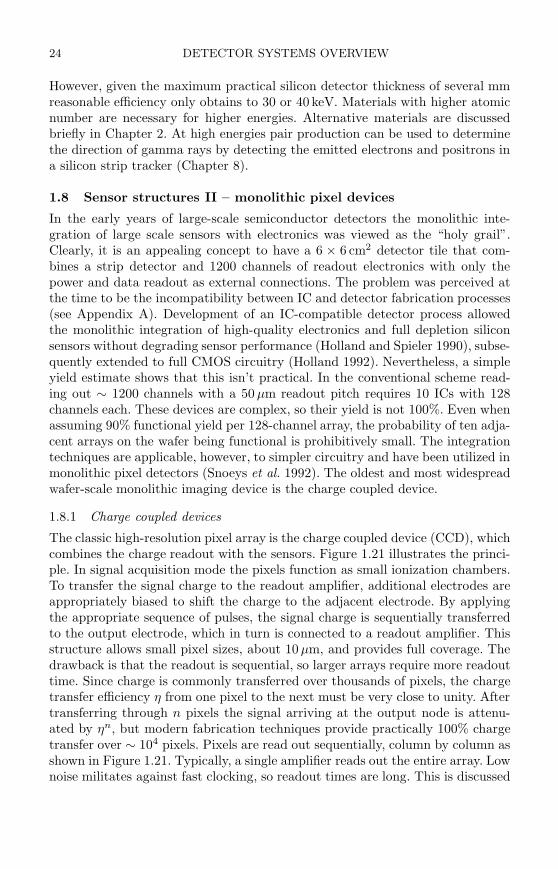
1.8.1 Charge coupled devices
The classic high-resolution pixel array is the charge coupled device (CCD), whichcombines the charge readout with the sensors. Figure 1.21 illustrates the princi-ple. In signal acquisition mode the pixels function as small ionization chambers.To transfer the signal charge to the readout amplifier, additional electrodes areappropriately biased to shift the charge to the adjacent electrode. By applyingthe appropriate sequence of pulses, the signal charge is sequentially transferredto the output electrode, which in turn is connected to a readout amplifier. Thisstructure allows small pixel sizes, about 10µm, and provides full coverage. Thedrawback is that the readout is sequential, so larger arrays require more readouttime. Since charge is commonly transferred over thousands of pixels, the chargetransfer efficiency η from one pixel to the next must be very close to unity. Aftertransferring through n pixels the signal arriving at the output node is attenu-ated by ηn, but modern fabrication techniques provide practically 100% chargetransfer over ∼ 104 pixels. Pixels are read out sequentially, column by column asshown in Figure 1.21. Typically, a single amplifier reads out the entire array. Lownoise militates against fast clocking, so readout times are long. This is discussed
SENSOR STRUCTURES II – MONOLITHIC PIXEL DEVICES 25
PARTICLE
TRACK
T1
T2
T3
T4
T6
T5
T1 T2 T3 T4 T5 T6 t
V
SERIAL OUTPUT REGISTER
PIXEL
ARRAY
OUTPUT
AMPLIFIER
Fig. 1.21. Upper right: schematic cross-sectional view of a CCD. Voltages are applied
to the electrodes according to the timing diagram at the upper left. The potential
sequence shifts the charge from the track to the right. Three electrodes comprise one
pixel, but all charge from the track subtended by the pixel is drawn to the pixel’s
left-most electrode. Six clock periods shift the charge to the neighboring pixel.
The pixels are read out sequentially (bottom left). Charge is transferred down the
column and then horizontally. The charge is deposited on a storage capacitor and
transferred to the readout line by the output amplifier.
in Chapter 4. Large arrays are commercially available; the SLD detector (Abeet al. 1997) used 16 × 80mm2 devices with 20 µm pixels. The sensitive depthwas 20 µm, so minimum ionizing particles yielded a broad charge distributionpeaking at about 1200 e. Electronic noise was 100 e. The thin depletion depthreduces the signal, but limits transverse diffusion and provides excellent positionresolution. The readout rate was 5MHz and four readout amplifiers were usedto speed up the readout. CCDs are in widespread use, but high-energy physicsand x-ray detection require specialized devices.
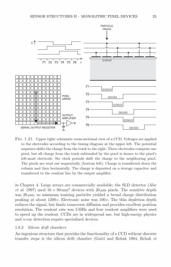
1.8.2 Silicon drift chambers
An ingenious structure that provides the functionality of a CCD without discretetransfer steps is the silicon drift chamber (Gatti and Rehak 1984, Rehak et
26 DETECTOR SYSTEMS OVERVIEW
TRACK
n
p
p
p+
+
+
V
V +V
0 VV
V
1
1 2
Fig. 1.22. Principle of a silicon drift chamber. The n-type bulk is depleted from
both surfaces by a series of p+ electrodes, biased to provide a positive potential
gradient along the center axis of the detector. Holes drift to the p electrodes, whereas
electrons are transported parallel to the surface and then attracted to the collection
electrode, where the signal is read out.
al. 1985). In this device a potential trough is established in the bulk, so thatthe signal charge is collected in the trough and then drifts towards the readoutelectrode (Figure 1.22). The position is derived from the time it takes for a signalcharge to move to the output, so the detector requires a time reference. When apulsed accelerator or pulsed x-ray tube is used, the start time is readily available.With random rates, as with radioactive sources, the time reference must bederived from the sensor. This will be discussed in Chapters 3 and 4. Althoughoriginally proposed as a position-sensing device, the Si drift chamber’s otheruseful application is energy spectroscopy. Since this structure collects chargefrom a large area onto a small collection electrode, the capacitance presented tothe readout amplifier is small (order 10 – 100 fF), so the electronic noise can bevery low. This can be exploited in x-ray detection and in photodiodes. Variousdrift detector topologies are described by Lutz (1999).
1.8.3 Monolithic active pixel sensors
Neither CCDs nor silicon drift devices can be fabricated using standard IC fabri-cation processes. The doping levels required for diode depletion widths of 100µmor more are much lower than used in commercial integrated circuits. The pro-cess complexity and yield requirements of the readout electronics needed formost application dictate the use of industry-standard fabrication processes. Incontrast to detectors, where the entire thickness of the silicon wafer is utilizedfor charge collection, integrated electronics utilize only a thin layer, of order µm,at the surface of the silicon. The remainder of the typically 500µm thick waferprovides mechanical support, but also serves to capture deleterious impurities,through gettering processes described in Appendix A. IC substrate material –typically grown by the Czochralski method – has both crystalline defects andimpurities, whereas detector grade material utilizes float-zone material, which is
SENSOR STRUCTURES II – MONOLITHIC PIXEL DEVICES 27
ELECTRONIC
S
SENSOR
METALLIZATION
p EPI
p BULK
n
+
VISIBLE LIGHT
p EPI (~1-10 m)µ
n WELL (~1 m)µ
p BULK
(300 - 500 m)µ
p-WELL WITH CIRCUITRY
+
TRACK
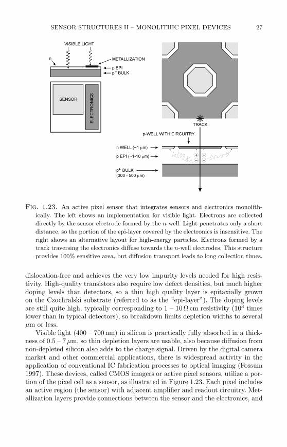
Fig. 1.23. An active pixel sensor that integrates sensors and electronics monolith-
ically. The left shows an implementation for visible light. Electrons are collected
directly by the sensor electrode formed by the n-well. Light penetrates only a short
distance, so the portion of the epi-layer covered by the electronics is insensitive. The
right shows an alternative layout for high-energy particles. Electrons formed by a
track traversing the electronics diffuse towards the n-well electrodes. This structure
provides 100% sensitive area, but diffusion transport leads to long collection times.
dislocation-free and achieves the very low impurity levels needed for high resis-tivity. High-quality transistors also require low defect densities, but much higherdoping levels than detectors, so a thin high quality layer is epitaxially grownon the Czochralski substrate (referred to as the “epi-layer”). The doping levelsare still quite high, typically corresponding to 1 – 10 Ω cm resistivity (103 timeslower than in typical detectors), so breakdown limits depletion widths to severalµm or less.
Visible light (400 – 700nm) in silicon is practically fully absorbed in a thick-ness of 0.5 – 7 µm, so thin depletion layers are usable, also because diffusion fromnon-depleted silicon also adds to the charge signal. Driven by the digital cameramarket and other commercial applications, there is widespread activity in theapplication of conventional IC fabrication processes to optical imaging (Fossum1997). These devices, called CMOS imagers or active pixel sensors, utilize a por-tion of the pixel cell as a sensor, as illustrated in Figure 1.23. Each pixel includesan active region (the sensor) with adjacent amplifier and readout circuitry. Met-allization layers provide connections between the sensor and the electronics, and
28 DETECTOR SYSTEMS OVERVIEW
between the components in the electronics cell. Light impinging on the sensoris detected, but is blocked by the metallization. Typical “fill factors”, the ratioof light-sensitive area to pixel area, are 20 – 30%, but this can be improved assmaller feature sizes shrink the electronics.
High-energy particles, on the other hand, traverse both the metallization andthe transistors, so devices have been developed that seek to utilize the epi-layerin the entire pixel as the sensor region, as shown in the right panel of Figure 1.23(Deptuch et al. 2003, Turchetta et al. 2003, Kleinfelder et al. 2004). Since thedepletion layers are thin, this device relies on diffusion for a substantial portionof the recovered charge. Thus, the recovered signal charge is much smaller thanin fully depleted detectors, about 1000 e compared to 22 000 e for a 300 µm thicksensor. Diffusion is channeled laterally by the potential well formed in the epi-layer, as it is lightly doped with respect to the substrate and the p-wells thataccommodate the electronics. Since the pixel capacitance is small, electronicnoise levels can also be low.
However, relying on diffusion increases the collection time to about 100ns,which can still provide the time resolution required at high-luminosity colliders,but radiation damage will degrade the carrier lifetime (see Appendix F) to order1 – 10ns after a relatively short time at high luminosity and the small radii wherepixel detectors are needed. Incomplete charge collection also limits the usabilityof these devices in applications that require good energy resolution, e.g. x-rayspectroscopy, although they may be acceptable for counting measurements.
The conceptually simplest form of an active pixel array is a matrix of tran-sistors. During image acquisition all transistors are inactive and signal chargeis stored on their input capacitance. Control electrodes are bussed by row andoutputs by column. During readout each transistor is addressed individually byselecting the appropriate row and all columns read out simultaneously. Thisstructure has been implemented by monolithically integrating the transistors(called DEPFETs) in a high-resistivity substrate (Kemmer and Lutz 1987). Thisarrangement allows the readout of individual pixels, but unlike more complexactive pixel devices can’t signal which pixels to read out. When reading out fullimage frames the performance of this structure is comparable to a CCD with afully parallel readout. Understanding the limits of this technique requires someadditional background, so we’ll return to it in Chapter 8.
Some active pixel designs replicate the fully sequential readout used forCCDs. This is a good match to digital photography, where every pixel carries in-formation. The electronic circuitry in each pixel cell is quite simple and readoutcan be slow, so the circuitry does not occupy much area. Slow readout appliedto charged particle detection also allows simple circuitry and facilitates low elec-tronic noise. However, in sparse data environments with high event rates, suchas high luminosity hadron colliders, “smart pixels” that signal the presence of ahit and then allow the selective readout of struck pixels sorted by time stamp arenecessary. This requires both fast response, to allow time stamping, and localthreshold discrimination, buffering, and readout logic. This drives up circuit com-
ELECTRONICS 29
plexity substantially, so the “real estate” occupied by the electronics increases,both in the pixel and in the common control and readout circuitry. This willbe illustrated in Chapter 8. Comparison of various technologies requires carefulscrutiny that the adopted architecture and circuit design match the intendedpurpose and not some simpler situation.
1.9 Electronics
Electronics are a key component of all modern detector systems. Although ex-periments and their associated electronics can take very different forms, the samebasic principles of the electronic readout and the optimization of signal-to-noiseratio apply to all.
The purpose of pulse processing and analysis systems is to
1. Acquire an electrical signal from the sensor. Typically this is a short currentpulse.
2. Tailor the time response of the system to optimize
(a) the minimum detectable signal (detect hit/no hit),(b) energy measurement,
(c) event rate,
(d) time of arrival (timing measurement),
(e) insensitivity to sensor pulse shape,
or some combination of the above.
3. Digitize the signal and store for subsequent analysis.
Position-sensitive detectors utilize the presence of a hit, amplitude measure-ment, or timing, so these detectors pose the same set of requirements. Generally,these properties cannot be optimized simultaneously, so compromises are neces-sary.
In addition to these primary functions of an electronic readout system, otherconsiderations can be equally or even more important, for example radiationresistance, low power (portable systems, large detector arrays, satellite systems),robustness, and – last, but not least – cost.
1.10 Detection limits and resolution
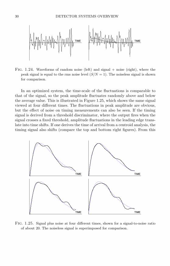
In addition to signal fluctuations originating in the sensor, the minimum detec-tion limit and energy resolution are subject to fluctuations introduced by theelectronics. The gain can be controlled very precisely, but electronic noise in-troduces baseline fluctuations, which are superimposed on the signal and alterthe peak amplitude. Figure 1.24 (left) shows a typical noise waveform. Both theamplitude and time distributions are random.
When superimposed on a signal, the noise alters both the amplitude andtime dependence. Figure 1.24 (right) shows the noise waveform superimposed ona small signal. As can be seen, the noise level determines the minimum signalwhose presence can be discerned.
30 DETECTOR SYSTEMS OVERVIEW
TIME TIME
Fig. 1.24. Waveforms of random noise (left) and signal + noise (right), where the
peak signal is equal to the rms noise level (S/N = 1). The noiseless signal is shown
for comparison.
In an optimized system, the time-scale of the fluctuations is comparable tothat of the signal, so the peak amplitude fluctuates randomly above and belowthe average value. This is illustrated in Figure 1.25, which shows the same signalviewed at four different times. The fluctuations in peak amplitude are obvious,but the effect of noise on timing measurements can also be seen. If the timingsignal is derived from a threshold discriminator, where the output fires when thesignal crosses a fixed threshold, amplitude fluctuations in the leading edge trans-late into time shifts. If one derives the time of arrival from a centroid analysis, thetiming signal also shifts (compare the top and bottom right figures). From this
TIME TIME
TIME TIME
Fig. 1.25. Signal plus noise at four different times, shown for a signal-to-noise ratio
of about 20. The noiseless signal is superimposed for comparison.
DETECTION LIMITS AND RESOLUTION 31
0
0.5
1
Qs/Q
n
NORMALIZEDCOUNTRATE
Qn
FWHM= 2.35 Qn
0.78
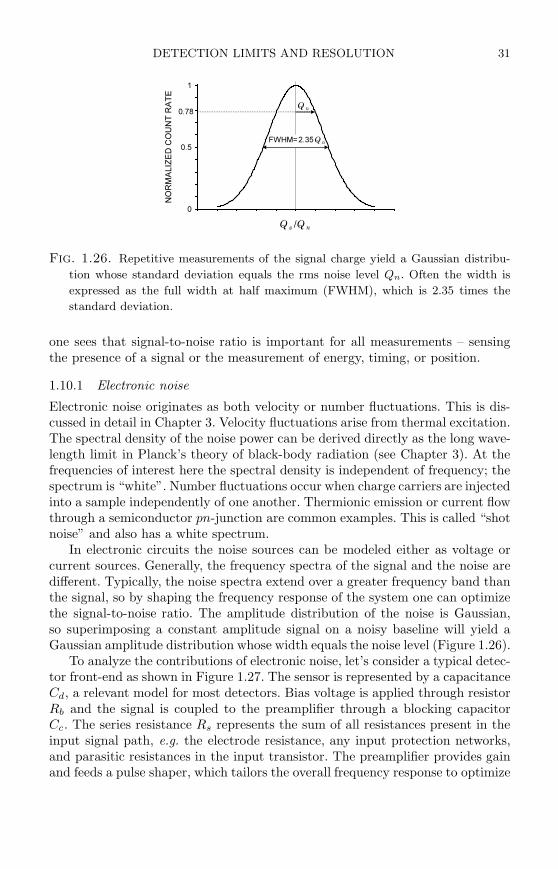
Fig. 1.26. Repetitive measurements of the signal charge yield a Gaussian distribu-
tion whose standard deviation equals the rms noise level Qn. Often the width is
expressed as the full width at half maximum (FWHM), which is 2.35 times the
standard deviation.
one sees that signal-to-noise ratio is important for all measurements – sensingthe presence of a signal or the measurement of energy, timing, or position.
1.10.1 Electronic noise
Electronic noise originates as both velocity or number fluctuations. This is dis-cussed in detail in Chapter 3. Velocity fluctuations arise from thermal excitation.The spectral density of the noise power can be derived directly as the long wave-length limit in Planck’s theory of black-body radiation (see Chapter 3). At thefrequencies of interest here the spectral density is independent of frequency; thespectrum is “white”. Number fluctuations occur when charge carriers are injectedinto a sample independently of one another. Thermionic emission or current flowthrough a semiconductor pn-junction are common examples. This is called “shotnoise” and also has a white spectrum.
In electronic circuits the noise sources can be modeled either as voltage orcurrent sources. Generally, the frequency spectra of the signal and the noise aredifferent. Typically, the noise spectra extend over a greater frequency band thanthe signal, so by shaping the frequency response of the system one can optimizethe signal-to-noise ratio. The amplitude distribution of the noise is Gaussian,so superimposing a constant amplitude signal on a noisy baseline will yield aGaussian amplitude distribution whose width equals the noise level (Figure 1.26).
To analyze the contributions of electronic noise, let’s consider a typical detec-tor front-end as shown in Figure 1.27. The sensor is represented by a capacitanceCd, a relevant model for most detectors. Bias voltage is applied through resistorRb and the signal is coupled to the preamplifier through a blocking capacitorCc. The series resistance Rs represents the sum of all resistances present in theinput signal path, e.g. the electrode resistance, any input protection networks,and parasitic resistances in the input transistor. The preamplifier provides gainand feeds a pulse shaper, which tailors the overall frequency response to optimize
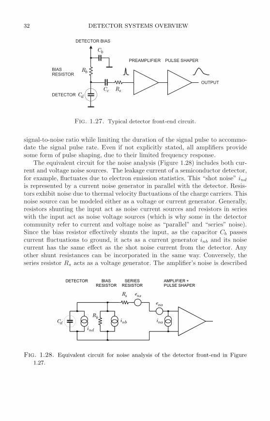
32 DETECTOR SYSTEMS OVERVIEW
OUTPUT
DETECTOR
BIAS
RESISTOR
Rb
Cc Rs
Cb
Cd
DETECTOR BIAS
PULSE SHAPERPREAMPLIFIER
Fig. 1.27. Typical detector front-end circuit.
signal-to-noise ratio while limiting the duration of the signal pulse to accommo-date the signal pulse rate. Even if not explicitly stated, all amplifiers providesome form of pulse shaping, due to their limited frequency response.
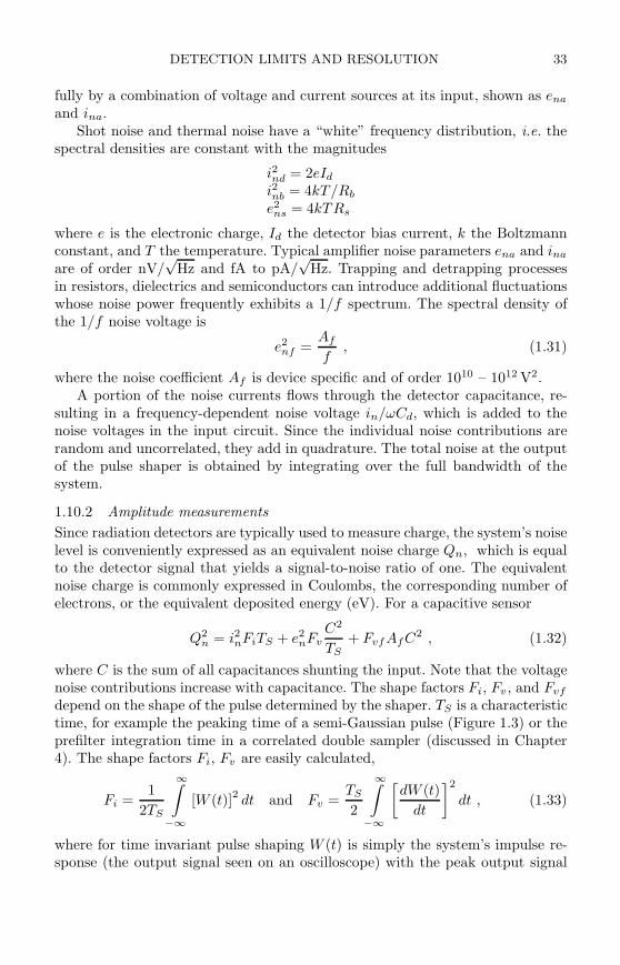
The equivalent circuit for the noise analysis (Figure 1.28) includes both cur-rent and voltage noise sources. The leakage current of a semiconductor detector,for example, fluctuates due to electron emission statistics. This “shot noise” ind
is represented by a current noise generator in parallel with the detector. Resis-tors exhibit noise due to thermal velocity fluctuations of the charge carriers. Thisnoise source can be modeled either as a voltage or current generator. Generally,resistors shunting the input act as noise current sources and resistors in serieswith the input act as noise voltage sources (which is why some in the detectorcommunity refer to current and voltage noise as “parallel” and “series” noise).Since the bias resistor effectively shunts the input, as the capacitor Cb passescurrent fluctuations to ground, it acts as a current generator inb and its noisecurrent has the same effect as the shot noise current from the detector. Anyother shunt resistances can be incorporated in the same way. Conversely, theseries resistor Rs acts as a voltage generator. The amplifier’s noise is described
DETECTOR
Cd
BIAS
RESISTOR
SERIES
RESISTOR
AMPLIFIER +
PULSE SHAPER
Rb
Rs
i
i i
e
e
nd
nb na
ns
na
Fig. 1.28. Equivalent circuit for noise analysis of the detector front-end in Figure
1.27.
DETECTION LIMITS AND RESOLUTION 33
fully by a combination of voltage and current sources at its input, shown as ena
and ina.Shot noise and thermal noise have a “white” frequency distribution, i.e. the
spectral densities are constant with the magnitudes
i2nd = 2eId
i2nb = 4kT/Rb
e2ns = 4kTRs
where e is the electronic charge, Id the detector bias current, k the Boltzmannconstant, and T the temperature. Typical amplifier noise parameters ena and ina
are of order nV/√
Hz and fA to pA/√
Hz. Trapping and detrapping processesin resistors, dielectrics and semiconductors can introduce additional fluctuationswhose noise power frequently exhibits a 1/f spectrum. The spectral density ofthe 1/f noise voltage is
e2nf =
Af
f, (1.31)
where the noise coefficient Af is device specific and of order 1010 – 1012 V2.A portion of the noise currents flows through the detector capacitance, re-
sulting in a frequency-dependent noise voltage in/ωCd, which is added to thenoise voltages in the input circuit. Since the individual noise contributions arerandom and uncorrelated, they add in quadrature. The total noise at the outputof the pulse shaper is obtained by integrating over the full bandwidth of thesystem.
1.10.2 Amplitude measurements
Since radiation detectors are typically used to measure charge, the system’s noiselevel is conveniently expressed as an equivalent noise charge Qn, which is equalto the detector signal that yields a signal-to-noise ratio of one. The equivalentnoise charge is commonly expressed in Coulombs, the corresponding number ofelectrons, or the equivalent deposited energy (eV). For a capacitive sensor
Q2n = i2nFiTS + e2
nFvC2
TS+ Fvf AfC2 , (1.32)
where C is the sum of all capacitances shunting the input. Note that the voltagenoise contributions increase with capacitance. The shape factors Fi, Fv , and Fvf
depend on the shape of the pulse determined by the shaper. TS is a characteristictime, for example the peaking time of a semi-Gaussian pulse (Figure 1.3) or theprefilter integration time in a correlated double sampler (discussed in Chapter4). The shape factors Fi, Fv are easily calculated,
Fi =1
2TS
∞∫
−∞
[W (t)]2 dt and Fv =TS
2
∞∫
−∞
[
dW (t)
dt
]2
dt , (1.33)
where for time invariant pulse shaping W (t) is simply the system’s impulse re-sponse (the output signal seen on an oscilloscope) with the peak output signal
34 DETECTOR SYSTEMS OVERVIEW
0.01 0.1 1 10 100
SHAPING TIME (µs)
102
103
104
EQUIVALENTNOISECHARGE(e)
CURRENT NOISE VOLTAGE NOISE
TOTAL
1/f NOISE
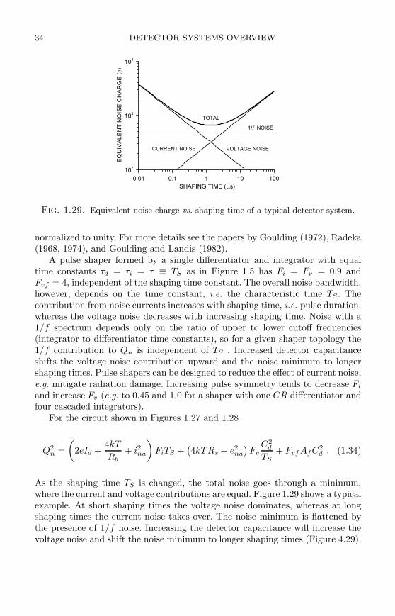
Fig. 1.29. Equivalent noise charge vs. shaping time of a typical detector system.
normalized to unity. For more details see the papers by Goulding (1972), Radeka(1968, 1974), and Goulding and Landis (1982).
A pulse shaper formed by a single differentiator and integrator with equaltime constants τd = τi = τ ≡ TS as in Figure 1.5 has Fi = Fv = 0.9 andFvf = 4, independent of the shaping time constant. The overall noise bandwidth,however, depends on the time constant, i.e. the characteristic time TS . Thecontribution from noise currents increases with shaping time, i.e. pulse duration,whereas the voltage noise decreases with increasing shaping time. Noise with a1/f spectrum depends only on the ratio of upper to lower cutoff frequencies(integrator to differentiator time constants), so for a given shaper topology the1/f contribution to Qn is independent of TS . Increased detector capacitanceshifts the voltage noise contribution upward and the noise minimum to longershaping times. Pulse shapers can be designed to reduce the effect of current noise,e.g. mitigate radiation damage. Increasing pulse symmetry tends to decrease Fi
and increase Fv (e.g. to 0.45 and 1.0 for a shaper with one CR differentiator andfour cascaded integrators).
For the circuit shown in Figures 1.27 and 1.28
Q2n =
(
2eId +4kT
Rb+ i2na
)
FiTS +(
4kTRs + e2na
)
FvC2
d
TS+ Fvf AfC2
d . (1.34)
As the shaping time TS is changed, the total noise goes through a minimum,where the current and voltage contributions are equal. Figure 1.29 shows a typicalexample. At short shaping times the voltage noise dominates, whereas at longshaping times the current noise takes over. The noise minimum is flattened bythe presence of 1/f noise. Increasing the detector capacitance will increase thevoltage noise and shift the noise minimum to longer shaping times (Figure 4.29).
DETECTION LIMITS AND RESOLUTION 35
For quick estimates one can use the following equation, which assumes a fieldeffect transistor (FET) amplifier (negligible ina) and a simple CR-RC shaperwith time constants τ (equal to the peaking time).
Q2n = 12
[
e2
nA · ns
]
Idτ + 6 · 105
[
e2 kΩ
ns
]
τ
Rb+ 3.6 · 104
[
e2 ns
(pF)2(nV)
2/Hz
]
e2n
C2
τ
For a given amplifier (i.e. en), noise is improved by reducing the detector ca-pacitance and leakage current, judiciously selecting all resistances in the inputcircuit, and choosing the optimum shaping time constant.
The noise parameters of the amplifier depend primarily on the input device.Chapter 6 treats this in detail. In field effect transistors the noise current contri-bution is very small, so reducing the detector leakage current and increasing thebias resistance will allow long shaping times with correspondingly lower noise.In bipolar transistors the base current sets a lower bound on the noise current,so these devices are best at short shaping times. In special cases where the noiseof a transistor scales with geometry, i.e. decreasing noise voltage with increasinginput capacitance, the lowest noise is obtained when the input capacitance of thetransistor is equal to the detector capacitance, albeit at the expense of powerdissipation. Capacitive matching is useful with FETs, but not bipolar transis-tors, as discussed in Chapter 6. In bipolar transistors the minimum obtainablenoise is independent of shaping time, but only at the optimum collector currentIC , which does depend on shaping time:
Q2n,min = 4kT
C√βDC
√
FiFv at IC =kT
eC√
βDC
√
Fv
Fi
1
TS, (1.35)
where βDC is the direct current gain. For a CR-RC shaper and βDC = 100,
Qn,min ≈ 250
[
e√pF
]
·√
C at IC = 260
[
µA · ns
pF
]
· C
TS. (1.36)
Practical noise levels range from < 1 e for CCDs at long shaping times to≈ 104 e in high-capacitance liquid argon calorimeters. Silicon strip detectors typ-ically operate at ≈ 103 e, whereas pixel detectors with fast readout can providenoise of order 100 e.
1.10.3 Timing measurements
In timing measurements the slope-to-noise ratio must be optimized, rather thanthe signal-to-noise ratio alone, so the rise time tr of the pulse is important. The“jitter” σt of the timing distribution
σt =σn
(dS/dt)ST
≈ trS/N
, (1.37)
where σn is the rms noise and the derivative of the signal dS/dt is evaluatedat the trigger level ST . To increase dS/dt without incurring excessive noise the
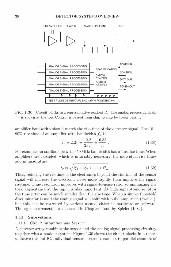
36 DETECTOR SYSTEMS OVERVIEW
PREAMPLIFIER SHAPER ANALOG PIPELINE ADC
ANALOG SIGNAL PROCESSING
ANALOG SIGNAL PROCESSING
ANALOG SIGNAL PROCESSING
ANALOG SIGNAL PROCESSING
ANALOG SIGNAL PROCESSING
TEST PULSE GENERATOR, DACs, R/ W POINTERS, etc.
SPARSIFICATION
DIGITAL
CONTROL
OUTPUT
DRIVERS
TOKEN IN
CONTROL
DATA OUT
TOKEN OUT
Fig. 1.30. Circuit blocks in a representative readout IC. The analog processing chain
is shown at the top. Control is passed from chip to chip by token passing.
amplifier bandwidth should match the rise-time of the detector signal. The 10 –90% rise time of an amplifier with bandwidth fu is
tr = 2.2τ =2.2
2πfu=
0.35
fu. (1.38)
For example, an oscilloscope with 350MHz bandwidth has a 1ns rise time. Whenamplifiers are cascaded, which is invariably necessary, the individual rise timesadd in quadrature
tr ≈√
t2r1 + t2r2 + . . . + t2rn . (1.39)
Thus, reducing the risetime of the electronics beyond the risetime of the sensorsignal will increase the electronic noise more rapidly than improve the signalrisetime. Time resolution improves with signal-to-noise ratio, so minimizing thetotal capacitance at the input is also important. At high signal-to-noise ratiosthe time jitter can be much smaller than the rise time. When a simple thresholddiscriminator is used the timing signal will shift with pulse amplitude (“walk”),but this can be corrected by various means, either in hardware or software.Timing measurements are discussed in Chapter 4 and by Spieler (1982).
1.11 Subsystems
1.11.1 Circuit integration and bussing
A detector array combines the sensor and the analog signal processing circuitrytogether with a readout system. Figure 1.30 shows the circuit blocks in a repre-sentative readout IC. Individual sensor electrodes connect to parallel channels of
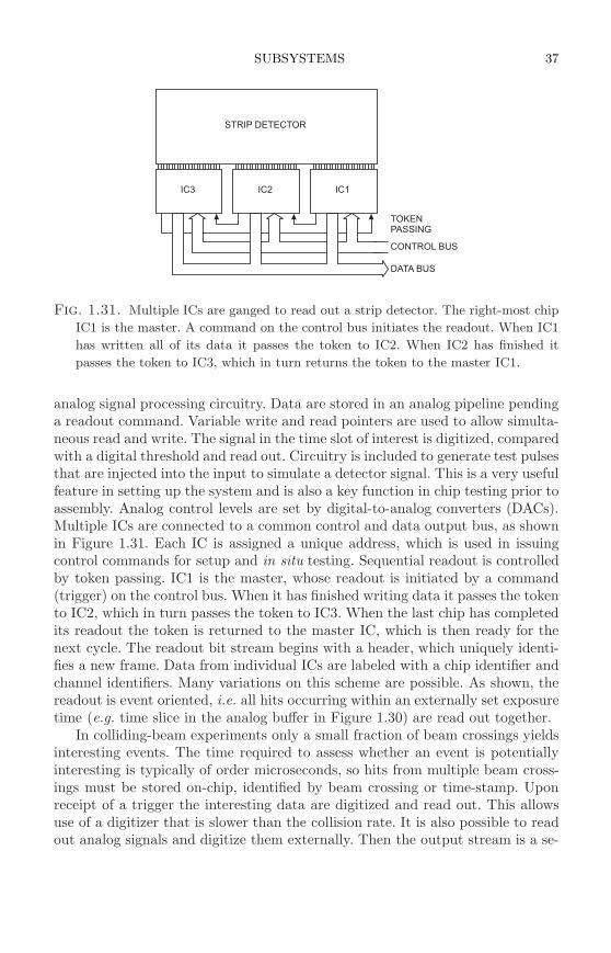
SUBSYSTEMS 37
CONTROL BUS
DATA BUS
TOKEN
PASSING
STRIP DETECTOR
IC3 IC2 IC1
Fig. 1.31. Multiple ICs are ganged to read out a strip detector. The right-most chip
IC1 is the master. A command on the control bus initiates the readout. When IC1
has written all of its data it passes the token to IC2. When IC2 has finished it
passes the token to IC3, which in turn returns the token to the master IC1.
analog signal processing circuitry. Data are stored in an analog pipeline pendinga readout command. Variable write and read pointers are used to allow simulta-neous read and write. The signal in the time slot of interest is digitized, comparedwith a digital threshold and read out. Circuitry is included to generate test pulsesthat are injected into the input to simulate a detector signal. This is a very usefulfeature in setting up the system and is also a key function in chip testing prior toassembly. Analog control levels are set by digital-to-analog converters (DACs).Multiple ICs are connected to a common control and data output bus, as shownin Figure 1.31. Each IC is assigned a unique address, which is used in issuingcontrol commands for setup and in situ testing. Sequential readout is controlledby token passing. IC1 is the master, whose readout is initiated by a command(trigger) on the control bus. When it has finished writing data it passes the tokento IC2, which in turn passes the token to IC3. When the last chip has completedits readout the token is returned to the master IC, which is then ready for thenext cycle. The readout bit stream begins with a header, which uniquely identi-fies a new frame. Data from individual ICs are labeled with a chip identifier andchannel identifiers. Many variations on this scheme are possible. As shown, thereadout is event oriented, i.e. all hits occurring within an externally set exposuretime (e.g. time slice in the analog buffer in Figure 1.30) are read out together.
In colliding-beam experiments only a small fraction of beam crossings yieldsinteresting events. The time required to assess whether an event is potentiallyinteresting is typically of order microseconds, so hits from multiple beam cross-ings must be stored on-chip, identified by beam crossing or time-stamp. Uponreceipt of a trigger the interesting data are digitized and read out. This allowsuse of a digitizer that is slower than the collision rate. It is also possible to readout analog signals and digitize them externally. Then the output stream is a se-
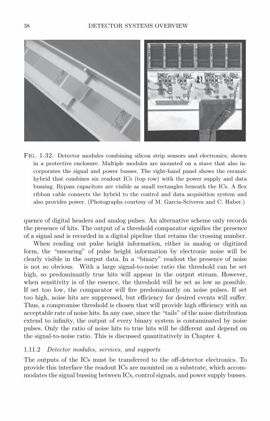
38 DETECTOR SYSTEMS OVERVIEW
Fig. 1.32. Detector modules combining silicon strip sensors and electronics, shown
in a protective enclosure. Multiple modules are mounted on a stave that also in-
corporates the signal and power busses. The right-hand panel shows the ceramic
hybrid that combines six readout ICs (top row) with the power supply and data
bussing. Bypass capacitors are visible as small rectangles beneath the ICs. A flex
ribbon cable connects the hybrid to the control and data acquisition system and
also provides power. (Photographs courtesy of M. Garcia-Sciveres and C. Haber.)
quence of digital headers and analog pulses. An alternative scheme only recordsthe presence of hits. The output of a threshold comparator signifies the presenceof a signal and is recorded in a digital pipeline that retains the crossing number.
When reading out pulse height information, either in analog or digitizedform, the “smearing” of pulse height information by electronic noise will beclearly visible in the output data. In a “binary” readout the presence of noiseis not so obvious. With a large signal-to-noise ratio the threshold can be sethigh, so predominantly true hits will appear in the output stream. However,when sensitivity is of the essence, the threshold will be set as low as possible.If set too low, the comparator will fire predominantly on noise pulses. If settoo high, noise hits are suppressed, but efficiency for desired events will suffer.Thus, a compromise threshold is chosen that will provide high efficiency with anacceptable rate of noise hits. In any case, since the “tails” of the noise distributionextend to infinity, the output of every binary system is contaminated by noisepulses. Only the ratio of noise hits to true hits will be different and depend onthe signal-to-noise ratio. This is discussed quantitatively in Chapter 4.
1.11.2 Detector modules, services, and supports
The outputs of the ICs must be transferred to the off-detector electronics. Toprovide this interface the readout ICs are mounted on a substrate, which accom-modates the signal bussing between ICs, control signals, and power supply busses.
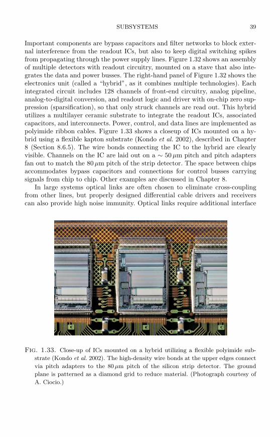
SUBSYSTEMS 39
Important components are bypass capacitors and filter networks to block exter-nal interference from the readout ICs, but also to keep digital switching spikesfrom propagating through the power supply lines. Figure 1.32 shows an assemblyof multiple detectors with readout circuitry, mounted on a stave that also inte-grates the data and power busses. The right-hand panel of Figure 1.32 shows theelectronics unit (called a “hybrid”, as it combines multiple technologies). Eachintegrated circuit includes 128 channels of front-end circuitry, analog pipeline,analog-to-digital conversion, and readout logic and driver with on-chip zero sup-pression (sparsification), so that only struck channels are read out. This hybridutilizes a multilayer ceramic substrate to integrate the readout ICs, associatedcapacitors, and interconnects. Power, control, and data lines are implemented aspolyimide ribbon cables. Figure 1.33 shows a closeup of ICs mounted on a hy-brid using a flexible kapton substrate (Kondo et al. 2002), described in Chapter8 (Section 8.6.5). The wire bonds connecting the IC to the hybrid are clearlyvisible. Channels on the IC are laid out on a ∼ 50 µm pitch and pitch adaptersfan out to match the 80 µm pitch of the strip detector. The space between chipsaccommodates bypass capacitors and connections for control busses carryingsignals from chip to chip. Other examples are discussed in Chapter 8.
In large systems optical links are often chosen to eliminate cross-couplingfrom other lines, but properly designed differential cable drivers and receiverscan also provide high noise immunity. Optical links require additional interface
Fig. 1.33. Close-up of ICs mounted on a hybrid utilizing a flexible polyimide sub-
strate (Kondo et al. 2002). The high-density wire bonds at the upper edges connect
via pitch adapters to the 80 µm pitch of the silicon strip detector. The ground
plane is patterned as a diamond grid to reduce material. (Photograph courtesy of
A. Ciocio.)
40 DETECTOR SYSTEMS OVERVIEW
ICs, as silicon is not well-suited for optical emitters. In some designs all driversare accommodated on the detector module, whereas in others multiple detectormodules interface through a common driver module.
1.11.3 Data acquisition
Signals are bussed from the detector modules to a readout module, which in-cludes data buffering. Depending on the complexity of the systems, several al-ternatives exist for interfacing to the data acquisition computer. Small systemscan interface directly via a plug-in card in a PC. In large systems VME or PCIbus interfaces are frequently used. In the past the nuclear instrumentation com-munity designed interfaces such as CAMAC or FastBus, but now the availabilityof suitable standard industry interfaces has displaced these community-specificinterfaces. The interface modules that accept the data from the detector moduleand transfer it to the computer data acquisition bus are usually custom designedand typically contain buffer memory, FPGA-based logic, and local processorsto preprocess the data. Digital interfacing utilizes standard techniques knownto many engineers and scientists, so it will not be covered in this book. For anoverview of data acquisition systems in high-energy physics see Butler (2003).
1.12 Further reading
The following chapters go into detail on the topics laid out in this introduction,but emphasize aspects relevant to large scale semiconductor systems. Books byG. Knoll (2000) and C. Grupen (1996) provide excellent general introductions toradiation detection and techniques. S.M. Sze (1981) gives a concise description ofsemiconductor physics and a comprehensive treatment of semiconductor devices.The following chapters and appendices include references to more specializedtexts.
References
Abe, K. et al. (1997). Design and performance of the SLD vertex detector: a307 Mpixel tracking system. Nucl. Instrum. and Meth. A400 (1997) 287–343
Barberis, E. et al. (1994). Capacitances in silicon microstrip detectors. Nucl.Instr. and Meth. A342 (1994) 90–95
Bedeschi, F. et al. (1989). CDF silicon detector prototype test beam results.IEEE Trans. Nucl Sci. NS-36 (1989) 35–39
Butler, J. (2003). Triggering and data acquisition general considerations, inInstrumentation in Elementary Particle Physics, AIP Conf. Proc. 674 (2003)101–129
Demaria, N. et al. (2000). New results on silicon microstrip detectors of CMStracker. Nucl. Instr. and Meth. A447 (2000) 142–150
Deptuch, G. et al. 2003. Development of monolithic active pixel sensors forcharged particle tracking. Nucl. Instr. and Meth. A511 (2003) 240–249
Fossum, E.R. (1997). CMOS image sensors: electronic camera on a chip. IEEE.Trans. Electron Dev. ED-44/10 (1997) 1689–1698
REFERENCES 41
Gatti, E. and Rehak, P. (1984). Semiconductor drift chamber – an applicationof a novel charge transport scheme. Nucl. Instr. and Meth. 225 (1984) 608–614
Goulding, F.S. (1972). Pulse shaping in low-noise nuclear amplifiers: a physicalapproach to noise analysis. Nucl. Instr. and Meth. 100 (1972) 493–504
Goulding, F.S. and Landis, D.A. (1982). Signal processing for semiconductordetectors. IEEE Trans. Nucl. Sci. NS-29/3 (1982) 1125–1141
Grupen, C. (1996). Particle Detectors. Cambridge University Press, Cambridge.ISBN 0-521-55216-8, QC787.G6G78
Holland, S. and Spieler, H. (1990). A monolithically integrated detector–pre-amplifier on high-resistivity silicon. IEEE Trans. Nucl. Sci. NS-37 (1990)463–468
Holland, S. (1992). Properties of CMOS Devices and circuits fabricated on high-resistivity, detector-grade Silicon. IEEE Trans. Nucl. Sci. NS-39/4 (1992)809–813
Kemmer, J. and Lutz, G. (1987). New detector concepts. Nucl. Instr. and Meth.A253 (1987) 365–377
Kenney, C. et al. (1993). Performance of a monolithic pixel detector. Nucl. Phys.B (Proc. Suppl.) 32 (1993) 460 and First test beam results from a monolithicsilicon pixel detector. Nucl. Instrum. and Meth. A326 (1993) 144–149
Kleinfelder, S.A. et al. (1988). A flexible 128 channel silicon strip detector in-strumentation integrated circuit with sparse data readout. IEEE Trans. Nucl.Sci. NS-35 (1988) 171–175
Kleinfelder, S.A. et al. (2004). Novel integrated CMOS sensor circuits. IEEETrans. Nucl. Sci. NS-51/5 (2004) 2328–2336
Knoll, G.F. (2000). Radiation Detection and Measurement(3rd edn). Wiley, NewYork, ISBN 0-471-07338-5, QC787.C6K56 1999
Kondo, T. et al. (2002). Construction and performance of the ATLAS siliconmicrostrip barrel modules. Nucl. Instr. and Meth. A485 (2002) 27–42
Luth, V. (1990). Spatial Resolution of Silicon Detectors. SLAC BaBar Note #549-7-90
Lutz, G. (1999). Semiconductor Radiation Detectors. Springer Verlag, Berlin,1999. ISBN 3-5406-4859-3
Particle Data Group (2004). Review of Particle Physics. Phys. Lett. B592(2004) 1–1109 and at http://pdg.lbl.gov
Radeka, V. (1968). Optimum signal-processing for pulse-amplitude spectrom-etry in the presence of high-rate effects and noise. IEEE Trans. Nucl. Sci.NS-15/3 (1968) 455–470
Radeka, V. (1974). Signal, noise and resolution in position-sensitive detectors.IEEE Trans. Nucl. Sci. NS-21 (1974) 51–64
Rehak, P. et al. (1985). Semiconductor drift chambers for position and energymeasurements. Nucl. Instrum. and Meth. A235 (1985) 224–234
Snoeys, W. et al. (1992). A new integrated pixel detector for high energyphysics. IEEE Trans. Nucl. Sci. 39 (1992) 1263–1269
42 DETECTOR SYSTEMS OVERVIEW
Spieler, H. (1982). Fast timing methods for semiconductor detectors. IEEETrans. Nucl. Sci. NS-29 (1982) 1142–1158
Sze, S.M. (1981). Physics of Semiconductor Devices(2nd edn). Wiley, New York1981. ISBN 0-471-05661-8, TK7871.85.S988
Turchetta, R. et al. (2003). Monolithic active pixel sensors (MAPS) in a VLSICMOS technology. Nucl. Instr. and Meth. A501 (2003) 251–259
Wood, M.L. et al. (1991). Charge correlation measurements of double-sideddirect-coupled silicon microstripe detectors. Supercollider 3 (J. Nonte, ed).Proc. 3rd Annual International Industrial Symposium on the Super Collider,Atlanta, Georgia, Mar 13–15, 1991. pp. 903–926. Plenum Press, New York.ISBN 0-3064-4037-7, QC787.P7.I57
PREFACE
When semiconductor detectors were introduced in the 1960s, their primary usewas in energy spectroscopy. By virtue of their dramatically improved energy res-olution they revolutionized gamma ray and charged particle spectroscopy. Detec-tor systems typically consisted of a single sensor, often cooled to liquid nitrogentemperature, and a bin filled with electronics, highly optimized for energy res-olution and count-rate capability. In the early 1980s a new development began,which would bring about a second revolution. Instead of emphasizing energy res-olution, these system exploited the micron-scale patterning capabilities of semi-conductor technology to form detectors with many electrodes as position-sensingdevices. Efficient readout of these detectors required high-density front-end elec-tronics. Detector systems now consisted of a highly segmented sensor, typicallywith strip electrodes on a 50 – 100 µm pitch, combined as a unit with an ar-ray of custom integrated circuits, often with 128 channels of readout electronicsper chip. These systems required a radically different design approach from pre-vious semiconductor detector systems. Rather than emphasizing primarily oneor two performance parameters, energy resolution and count-rate performance,these systems needed to fulfill many conflicting requirements, i.e. low noise, lowpower and minimum material. Later – in systems for high-luminosity colliders –additional demands on fast timing and radiation resistance had to be met.
So different were these requirements from the established paradigm, that con-ventional wisdom among the experts held these systems to be impractical, if notimpossible. Today, highly integrated semiconductor detector systems with tensof thousands of channels are routine and new detectors are under constructioncovering hundreds of square meters with millions of channels. Although advancesin technology – especially in integrated circuit density – have played a major rolein bringing this about, this development required more than the magic of moderntechnology. These systems are bounded by rather fundamental constraints, whichwere already well-understood in the 1970s. The challenge was to take a fresh lookat these constraints and develop new architectures that balanced experimentaldemands with practical technology.
The goal of this book is to show how this balance comes about, so it em-phasizes both sensors and electronics as a system. It is written primarily forphysicists who devise new detectors and bring them into operation, so I includebasic discussions of amplifiers, circuits, and electronic noise that are familiar toengineers, but not covered in a typical physics curriculum. The choice of top-ics and the organization of the book resulted from courses I have taught in thePhysics Department of the University of California at Berkeley and from numer-ous short courses on detectors and signal processing on six continents, rangingfrom the undergraduate to the faculty level. Much of the material was developed
v
vi PREFACE
in my attempts to educate my collaborators and the reviewers of funding propos-als. The exposition of topics results from many interactions with students, whoon occasion have made abundantly clear to me what doesn’t work. This has ledto a “cyclical” approach, where I return to topics for more detailed discussionsand reiterate explanations in different contexts. This does lead to some redun-dancy, but also allows chapters to be read individually, although they do buildon one another.
Since new detectors will be always be stretching the envelope, it is importantto understand the basic principles underlying the technology to see how far onecan push, so I emphasize physical principles and how they are applied. Althoughthe big picture is important, details are crucial, so in important areas I go intosome detail, especially in the sections on noise, signal processing and devices.What I don’t do, is delve deeply into the intricacies of detector technology andcircuit design. Engineers have developed very powerful analysis techniques andtechnological tools that are essential for a working design. Fortunately, knowl-edge of sensor and IC fabrication details, complex frequency space, and Laplacetransforms is not needed to understand the key principles of the systems and thengo to the experts with the right questions. This is not a cookbook. Technologyprogresses continually, so specific examples are included to illustrate concepts,rather than prescriptions for designs. I emphasize the key mechanisms and theirinterplay, with the goal of helping readers focus the analysis of their own de-signs, as the usual curricula tend to teach how to calculate, rather than what tocalculate.
The foundations provided by a good undergraduate physics education shouldbe sufficient to follow the discussions in this book. The book is designed to beself-contained. Key elements are derived, to make clear their origins and limits.Some of the derivations can be found readily in the more specialized literature,but I’ve included them since it allows me to emphasize those aspects that areimportant for this specific application, for example in the diode equation andthe treatment of the bipolar transistor. Whenever the derivations would disruptthe main thread of the discussion, I’ve moved them to the appendices. For thosewho are not familiar with equivalent circuits or with complex notation to describephase shifts, brief tutorial descriptions are also included as appendices.
Chapter 1 gives an overview and summarizes key aspects of semiconductordetector arrays to provide context for the subsequent more detailed discussions.It can also serve as an executive summary for those who wish to appear knowl-edgeable without going to the trouble of understanding too much. Chapters 2and 3 cover signal formation and electronic noise and lead to Chapter 4, whichdiscusses signal processing and optimization of signal-to-noise ratio. Chapter 5discusses digitization techniques, including their flaws, which provides some keyinsights needed for a brief introduction to digital signal processing. Up to thispoint the discussions are largely technology-independent, i.e. these principlescan be applied to either old or new technology and remain valid as technologyprogresses. Technology limits enter into Chapter 6, Transistors and Amplifiers,
PREFACE vii
which discusses how technology affects the device parameters that are critical indetector systems. This gives insight into practical noise limits and also providesthe basis for Chapter 7, which discusses radiation effects and mitigation tech-niques. This area shows clearly how degradation of individual device propertiescan be mitigated by system architecture and appropriate choice of system pa-rameters. Chapter 8 selects some specific detector designs to illustrate conflictsand trade-offs, and shows how different solutions address the same goals. Thischapter also includes some comments on design and assembly techniques, reli-ability issues, and testing. In closing, Chapter 9 turns to what is probably themost important problem, why things don’t work. Although not exhaustive, itdiscusses many of the interference sources and design flaws that cause systemsto perform more poorly than expected, or even be unusable. This is a complextopic, rife with simple recipes, which tend to be wrong.
In the past two decades semiconductor detector arrays have come a longway. We have encountered many difficulties that were not foreseen, but silicontechnology is mature and highly developed, so the power of the technology hasalways provided the flexibility to find solutions. Although the next generationof detector arrays is still under construction, future accelerator upgrades nowunder discussion will tax detector capabilities even more. Furthermore, we seedevelopments coming full circle. After being driven by tracking applications inhigh-energy physics, we now see increasing interest in applying array technologyto x-ray spectroscopy for astrophysics, materials science, and medical imaging.Even though the requirements are daunting and solutions not always obvious,we can be assured that semiconductor detector arrays will be key componentsin frontier experiments for years to come.
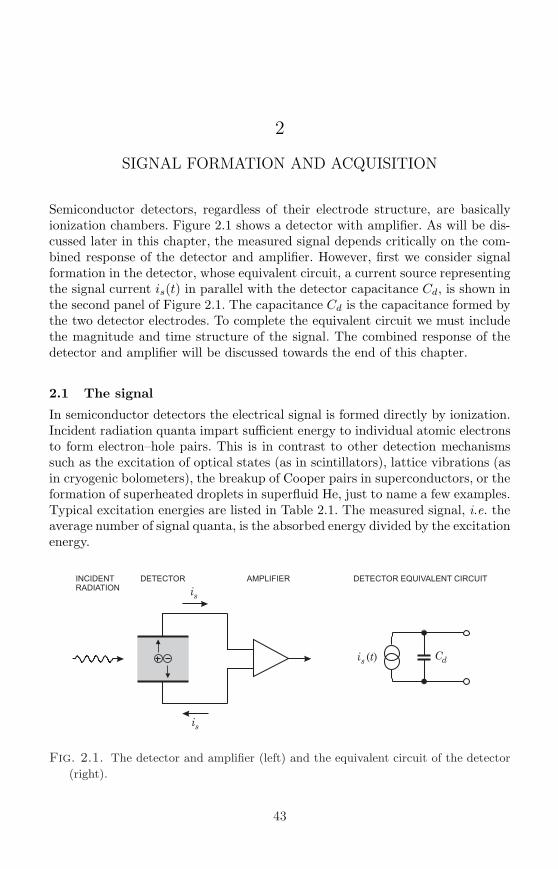
2
SIGNAL FORMATION AND ACQUISITION
Semiconductor detectors, regardless of their electrode structure, are basicallyionization chambers. Figure 2.1 shows a detector with amplifier. As will be dis-cussed later in this chapter, the measured signal depends critically on the com-bined response of the detector and amplifier. However, first we consider signalformation in the detector, whose equivalent circuit, a current source representingthe signal current is(t) in parallel with the detector capacitance Cd, is shown inthe second panel of Figure 2.1. The capacitance Cd is the capacitance formed bythe two detector electrodes. To complete the equivalent circuit we must includethe magnitude and time structure of the signal. The combined response of thedetector and amplifier will be discussed towards the end of this chapter.
2.1 The signal
In semiconductor detectors the electrical signal is formed directly by ionization.Incident radiation quanta impart sufficient energy to individual atomic electronsto form electron–hole pairs. This is in contrast to other detection mechanismssuch as the excitation of optical states (as in scintillators), lattice vibrations (asin cryogenic bolometers), the breakup of Cooper pairs in superconductors, or theformation of superheated droplets in superfluid He, just to name a few examples.Typical excitation energies are listed in Table 2.1. The measured signal, i.e. theaverage number of signal quanta, is the absorbed energy divided by the excitationenergy.
AMPLIFIERDETECTOR DETECTOR EQUIVALENT CIRCUIT
i
i
s
s
Ci ds
INCIDENT
RADIATION
( )t
Fig. 2.1. The detector and amplifier (left) and the equivalent circuit of the detector
(right).
43
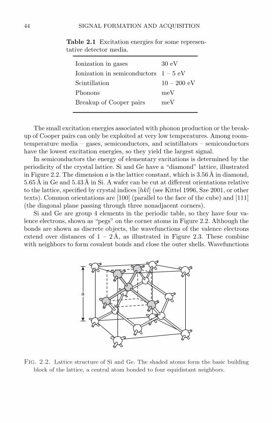
44 SIGNAL FORMATION AND ACQUISITION
Table 2.1 Excitation energies for some represen-tative detector media.
Ionization in gases 30 eV
Ionization in semiconductors 1 – 5 eV
Scintillation 10 – 200 eV
Phonons meV
Breakup of Cooper pairs meV
The small excitation energies associated with phonon production or the break-up of Cooper pairs can only be exploited at very low temperatures. Among room-temperature media – gases, semiconductors, and scintillators – semiconductorshave the lowest excitation energies, so they yield the largest signal.
In semiconductors the energy of elementary excitations is determined by theperiodicity of the crystal lattice. Si and Ge have a “diamond” lattice, illustratedin Figure 2.2. The dimension a is the lattice constant, which is 3.56 A in diamond,5.65 A in Ge and 5.43 A in Si. A wafer can be cut at different orientations relativeto the lattice, specified by crystal indices [hkl] (see Kittel 1996, Sze 2001, or othertexts). Common orientations are [100] (parallel to the face of the cube) and [111](the diagonal plane passing through three nonadjacent corners).
Si and Ge are group 4 elements in the periodic table, so they have four va-lence electrons, shown as “pegs” on the corner atoms in Figure 2.2. Although thebonds are shown as discrete objects, the wavefunctions of the valence electronsextend over distances of 1 – 2 A, as illustrated in Figure 2.3. These combinewith neighbors to form covalent bonds and close the outer shells. Wavefunctions
a
Fig. 2.2. Lattice structure of Si and Ge. The shaded atoms form the basic building
block of the lattice, a central atom bonded to four equidistant neighbors.
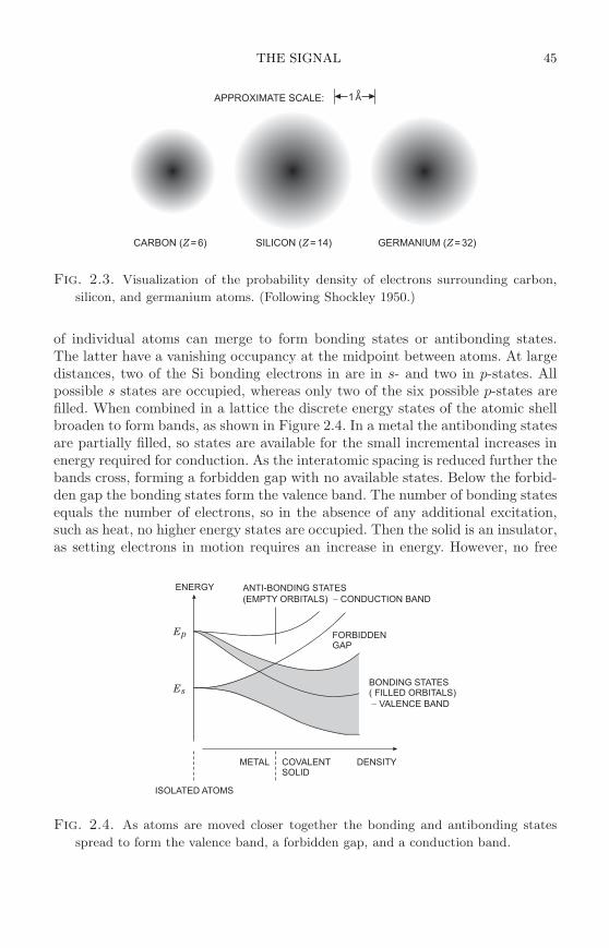
THE SIGNAL 45
CARBON ( =6)Z SILICON ( =14)Z GERMANIUM ( =32)Z
1 AAPPROXIMATE SCALE:
Fig. 2.3. Visualization of the probability density of electrons surrounding carbon,
silicon, and germanium atoms. (Following Shockley 1950.)
of individual atoms can merge to form bonding states or antibonding states.The latter have a vanishing occupancy at the midpoint between atoms. At largedistances, two of the Si bonding electrons in are in s- and two in p-states. Allpossible s states are occupied, whereas only two of the six possible p-states arefilled. When combined in a lattice the discrete energy states of the atomic shellbroaden to form bands, as shown in Figure 2.4. In a metal the antibonding statesare partially filled, so states are available for the small incremental increases inenergy required for conduction. As the interatomic spacing is reduced further thebands cross, forming a forbidden gap with no available states. Below the forbid-den gap the bonding states form the valence band. The number of bonding statesequals the number of electrons, so in the absence of any additional excitation,such as heat, no higher energy states are occupied. Then the solid is an insulator,as setting electrons in motion requires an increase in energy. However, no free
E
E
p
s
ENERGY
FORBIDDENGAP
ANTI-BONDING STATES
(EMPTY ORBITALS) CONDUCTION BAND
BONDING STATES( FILLED ORBITALS)
VALENCE BAND
DENSITY
ISOLATED ATOMS
METAL COVALENTSOLID
Fig. 2.4. As atoms are moved closer together the bonding and antibonding states
spread to form the valence band, a forbidden gap, and a conduction band.
46 SIGNAL FORMATION AND ACQUISITION
DISTANCEDENSITY OF STATES
EN
ER
GY
EN
ER
GY
CONDUCTION BAND CONDUCTION BAND
VALENCE BAND VALENCE BAND
CORE ELECTRONS
FORBIDDEN GAP
FORBIDDEN GAP
Fig. 2.5. Density of states (energy levels per unit volume) and band structure. Al-
though the band structure is commonly shown in simplified form, as in the right–
hand panel, the density of states within the band varies greatly with energy (left).
(Following Shockley 1950.)
states are available in the valence band. This requires promoting electrons acrossthe forbidden gap to the empty orbitals above, so this set of states is called theconduction band.
Each atom in the lattice contributes its quantum states to each band, sothat the number of quantum states in the band is equal to the number of statesfrom which the band was formed, i.e. at least one for each atom in the lattice.Since the density of atoms in Si is 5.0 · 1022 cm−3, many states can be available.Although they comprise energy levels originally associated with individual atoms,the bands are extended states, i.e. the state contributed by an individual atomextends throughout the crystal.
Si
Si
Si
Si
Si
Si
Si
SiSILICON ATOM WITH FOUR
VALENCE ELECTRONS
SYMBOLIC PLANE VIEW USING
LINES TO REPRESENT BONDS
SILICON “CORES” WITH ELECTRON
“CLOUDS” SHOWING VALENCE PAIR BONDS
Fig. 2.6. Bonds in a diamond lattice shown schematically. (Following Shockley 1950.)
THE SIGNAL 47
Si SiSi Si
Si SiSi Si
Si SiSi Si
Si SiSi Si
Si SiSi Si
Si Si
Si Si
Si Si
Si Si
Si Si
Si Si
Si Si
Si Si
NET MOTION
OF ELECTRON
NET MOTION
OF HOLE
INCIDENT PHOTON BREAKS BOND
MOTION OF
REPLACEMENT
ELECTRONS
ELECTRIC FIELD
Fig. 2.7. An incident particle can break a bond, promoting an electron into the
conduction band, so it can move freely. The vacant bond with positive net charge can
also move by successively “borrowing” electrons from neighboring bonds. (Following
Shockley 1950.)
The density of states is not uniform; it depends on energy, as shown in the leftside of Figure 2.5. In space, the bands extend uniformly throughout the crystal,as shown in the right side of Figure 2.5. Typical widths of the forbidden bandare 0.7 eV in Ge, 1.1 eV in Si, 1.4 eV in GaAs and 5.5 eV in diamond.
Figure 2.6 shows the bonds in a diamond lattice schematically. At 0K allelectrons occupy bonding states, completely filling the valence band and, as notedabove, no electrical conduction is possible, as no states are available withoutimparting the substantial energy to surmount the bandgap.
However, if energy is imparted to a bond by incident radiation, for examplea photon, the bond can be broken. This excites an electron into the conductionband and leaves back a vacant state in the valence band, a “hole”, as illustratedin Figure 2.7. The electron can move freely in its extended state in the conductionband. However, although the hole appears in the valence band, it can also move,albeit by an indirect mechanism. Since the vacant state is completely equivalentto those contributed other atoms, the hole can be filled by an electron from anearby atom, thereby moving to another position.
The motion of the electron and hole can be directed by an electric field. Holescan be treated as positive charge carriers just like the electrons, although theytend to move more slowly as hole transport involves sequential transition proba-bilities (the wavefunction overlap of the hole and its replacement electron). Thus,the absorbing volume acts as an ionization chamber. The minimum detectablequantum of energy is set by the bandgap. Larger absorbed energies can promotemultiple electrons into the conduction band, yielding a correspondingly largersignal.
Although it is intuitively obvious that a discrete energy deposition can excitean electron from the valence into the conduction band, it is not so obvious what
48 SIGNAL FORMATION AND ACQUISITION
the effect of thermal excitation is. After all, at room temperature, thermal energyis about 1/40eV, which is much smaller than the bandgap.
In a pure semiconductor electrons in the conduction band can only originatethrough thermal excitation from the valence band, so the concentration of elec-trons and holes must be equal. Since electrons are fermions, the probability ofoccupying an energy state is given by the Fermi–Dirac distribution
fe(E) =1
e(E−EF )/kT + 1, (2.1)
where EF is the Fermi level (equal to the chemical potential in thermodynamics).The probability of a hole state not being occupied, i.e. a valence state beingempty, is
fh(E) = 1 − fe(E) =1
e(EF −E)/kT + 1, (2.2)
so equal concentrations of electrons and holes place the Fermi level in the middleof the bandgap EF = Eg/2, the “intrinsic” level. In silicon the bandgap energyEg = 1.12 eV. For a thermal energy of 26 meV the probability of an electronoccupying a state in the conduction band is 4.4 · 10−10. Nevertheless, becauseof the high density of states, the intrinsic carrier concentration ni = 1.45 · 1010
cm−3, corresponding to a resistivity of about 3 · 105 Ω cm.From this we see what distinguishes insulators from semiconductors. At 0K
semiconductors are insulators, but at higher temperatures they have substantialconductivity, depending on the magnitude of the bandgap. Insulators have suf-ficiently large bandgaps so that the concentration of carriers in the conductionband is negligible at all temperatures of interest.
In a radiation sensor, thermal excitation leads to a continuous current flow,from which the presence of any radiation signal must be distinguished. Further-more, as was shown in Chapter 1, random fluctuations in the quiescent currentflow limit the precision with which the background can be measured, which alsosets a minimum signal threshold. A large bandgap greatly reduces the thermallyexcited current, but reduces the number of charge pairs due to the desired signal.Conversely, a small bandgap increases the signal, but leads to an exponential in-crease in background current. Furthermore, in applications that require timinginformation or high pulse rates the signal charge should be swept rapidly fromthe sensitive volume, so it is important to establish a high electric field. Thus, theconductivity of the sensor material must be low, to allow application of an appro-priate voltage without excessive current flow. As a result, the range of bandgapssuitable for practical radiation sensors is quite limited. These considerations aresummarized in Table 2.2.
2.2 Detector sensitivity
2.2.1 Low energy quanta (E ≈ Eg)
The ionization energy in solids is proportional to the bandgap, so the bandgapsets the minimum detection threshold. At incident energies below the gap energy,
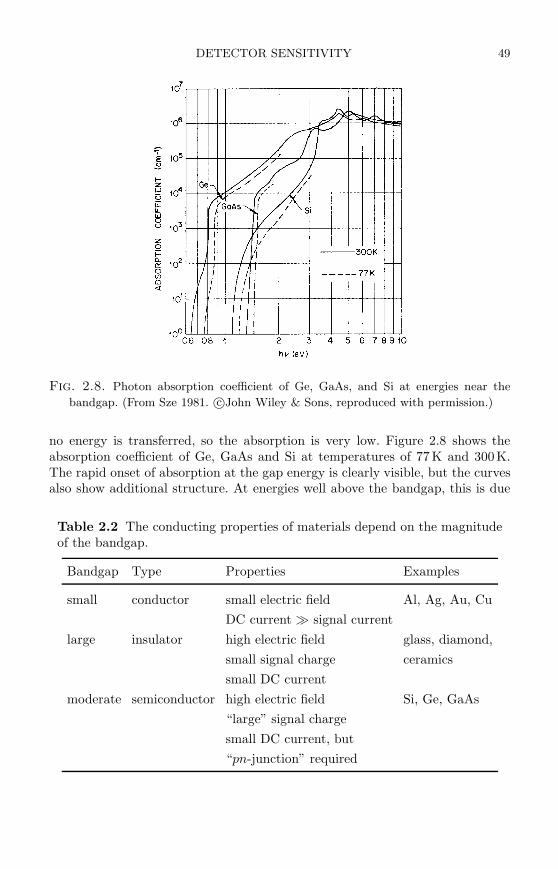
DETECTOR SENSITIVITY 49
Fig. 2.8. Photon absorption coefficient of Ge, GaAs, and Si at energies near the
bandgap. (From Sze 1981. c©John Wiley & Sons, reproduced with permission.)
no energy is transferred, so the absorption is very low. Figure 2.8 shows theabsorption coefficient of Ge, GaAs and Si at temperatures of 77K and 300K.The rapid onset of absorption at the gap energy is clearly visible, but the curvesalso show additional structure. At energies well above the bandgap, this is due
Table 2.2 The conducting properties of materials depend on the magnitudeof the bandgap.
Bandgap Type Properties Examples
small conductor small electric field Al, Ag, Au, Cu
DC current ≫ signal current
large insulator high electric field glass, diamond,
small signal charge ceramics
small DC current
moderate semiconductor high electric field Si, Ge, GaAs
“large” signal charge
small DC current, but
“pn-junction” required
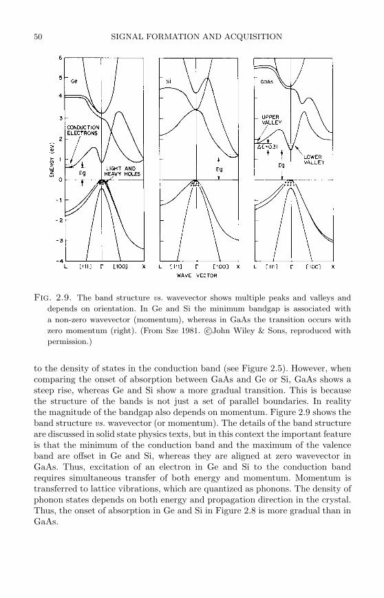
50 SIGNAL FORMATION AND ACQUISITION
Fig. 2.9. The band structure vs. wavevector shows multiple peaks and valleys and
depends on orientation. In Ge and Si the minimum bandgap is associated with
a non-zero wavevector (momentum), whereas in GaAs the transition occurs with
zero momentum (right). (From Sze 1981. c©John Wiley & Sons, reproduced with
permission.)
to the density of states in the conduction band (see Figure 2.5). However, whencomparing the onset of absorption between GaAs and Ge or Si, GaAs shows asteep rise, whereas Ge and Si show a more gradual transition. This is becausethe structure of the bands is not just a set of parallel boundaries. In realitythe magnitude of the bandgap also depends on momentum. Figure 2.9 shows theband structure vs. wavevector (or momentum). The details of the band structureare discussed in solid state physics texts, but in this context the important featureis that the minimum of the conduction band and the maximum of the valenceband are offset in Ge and Si, whereas they are aligned at zero wavevector inGaAs. Thus, excitation of an electron in Ge and Si to the conduction bandrequires simultaneous transfer of both energy and momentum. Momentum istransferred to lattice vibrations, which are quantized as phonons. The density ofphonon states depends on both energy and propagation direction in the crystal.Thus, the onset of absorption in Ge and Si in Figure 2.8 is more gradual than inGaAs.
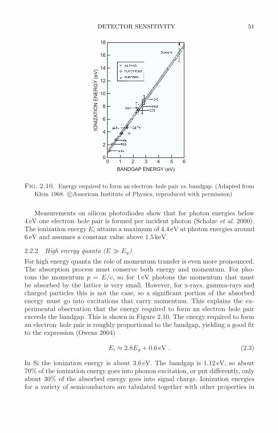
DETECTOR SENSITIVITY 51
2
0
4
6
8
18
16
14
12
10
10 2 3 4 5 6
BANDGAP ENERGY (eV)
ION
IZA
TIO
NE
NE
RG
Y(e
V)
Fig. 2.10. Energy required to form an electron–hole pair vs. bandgap. (Adapted from
Klein 1968. c©American Institute of Physics, reproduced with permission)
Measurements on silicon photodiodes show that for photon energies below4 eV one electron–hole pair is formed per incident photon (Scholze et al. 2000).The ionization energy Ei attains a maximum of 4.4 eV at photon energies around6 eV and assumes a constant value above 1.5 keV.
2.2.2 High energy quanta (E ≫ Eg)
For high energy quanta the role of momentum transfer is even more pronounced.The absorption process must conserve both energy and momentum. For pho-tons the momentum p = E/c, so for 1 eV photons the momentum that mustbe absorbed by the lattice is very small. However, for x-rays, gamma-rays andcharged particles this is not the case, so a significant portion of the absorbedenergy must go into excitations that carry momentum. This explains the ex-perimental observation that the energy required to form an electron–hole pairexceeds the bandgap. This is shown in Figure 2.10. The energy required to forman electron–hole pair is roughly proportional to the bandgap, yielding a good fitto the expression (Owens 2004)
Ei ≈ 2.8Eg + 0.6 eV . (2.3)
In Si the ionization energy is about 3.6 eV. The bandgap is 1.12 eV, so about70% of the ionization energy goes into phonon excitation, or put differently, onlyabout 30% of the absorbed energy goes into signal charge. Ionization energiesfor a variety of semiconductors are tabulated together with other properties in
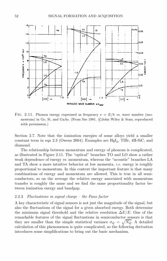
52 SIGNAL FORMATION AND ACQUISITION
Fig. 2.11. Phonon energy expressed as frequency ν = E/h vs. wave number (mo-
mentum) in Ge, Si, and GaAs. (From Sze 1981. c©John Wiley & Sons, reproduced
with permission.)
Section 2.7. Note that the ionization energies of some alloys yield a smallerconstant term in eqn 2.3 (Owens 2004). Examples are HgI2, TlBr, 4H-SiC, anddiamond.
The relationship between momentum and energy of phonons is complicated,as illustrated in Figure 2.11. The “optical” branches TO and LO show a ratherweak dependence of energy vs. momentum, whereas the “acoustic” branches LAand TA show a more intuitive behavior at low momenta, i.e. energy is roughlyproportional to momentum. In this context the important feature is that manycombinations of energy and momentum are allowed. This is true in all semi-conductors, so on the average the relative energy associated with momentumtransfer is roughly the same and we find the same proportionality factor be-tween ionization energy and bandgap.
2.2.3 Fluctuations in signal charge – the Fano factor
A key characteristic of signal sensors is not just the magnitude of the signal, butalso the fluctuations of the signal for a given absorbed energy. Both determinethe minimum signal threshold and the relative resolution ∆E/E. One of theremarkable features of the signal fluctuations in semiconductor sensors is thatthey are smaller than the simple statistical variance σQ =
√
NQ. A detailedcalculation of this phenomenon is quite complicated, so the following derivationintroduces some simplifications to bring out the basic mechanism.
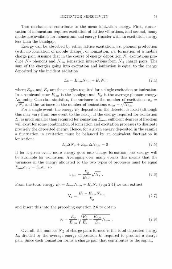
DETECTOR SENSITIVITY 53
Two mechanisms contribute to the mean ionization energy. First, conser-vation of momentum requires excitation of lattice vibrations, and second, manymodes are available for momentum and energy transfer with an excitation energyless than the bandgap.
Energy can be absorbed by either lattice excitation, i.e. phonon production(with no formation of mobile charge), or ionization, i.e. formation of a mobilecharge pair. Assume that in the course of energy deposition Nx excitations pro-duce NP phonons and Nion ionization interactions form NQ charge pairs. Thesum of the energies going into excitation and ionization is equal to the energydeposited by the incident radiation
E0 = EionNion + ExNx , (2.4)
where Eion and Ex are the energies required for a single excitation or ionization.In a semiconductor Eion is the bandgap and Ex is the average phonon energy.Assuming Gaussian statistics, the variance in the number of excitations σx =√
Nx and the variance in the number of ionizations σion =√
Nion.For a single event, the energy E0 deposited in the detector is fixed (although
this may vary from one event to the next). If the energy required for excitationEx is much smaller than required for ionization Eion, sufficient degrees of freedomwill exist for some combination of ionization and excitation processes to dissipateprecisely the deposited energy. Hence, for a given energy deposited in the samplea fluctuation in excitation must be balanced by an equivalent fluctuation inionization:
Ex∆Nx + Eion∆Nion = 0 . (2.5)
If for a given event more energy goes into charge formation, less energy willbe available for excitation. Averaging over many events this means that thevariances in the energy allocated to the two types of processes must be equalEionσion = Exσx, so
σion =Ex
Eion
√
Nx . (2.6)
From the total energy E0 = EionNion + ExNx (eqn 2.4) we can extract
Nx =E0 − EionNion
Ex(2.7)
and insert this into the preceding equation 2.6 to obtain
σi =Ex
Eion
√
E0
Ex− Eion
ExNion . (2.8)
Overall, the number NQ of charge pairs formed is the total deposited energyE0 divided by the average energy deposition Ei required to produce a chargepair. Since each ionization forms a charge pair that contributes to the signal,
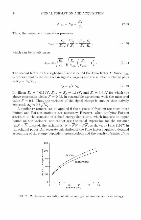
54 SIGNAL FORMATION AND ACQUISITION
Nion = NQ =E0
Ei. (2.9)
Thus, the variance in ionization processes
σion =Ex
Eion
√
E0
Ex− Eion
Ex
E0
Ei, (2.10)
which can be rewritten as
σion =
√
E0
Ei·√
Ex
Eion
(
Ei
Eion− 1
)
. (2.11)
The second factor on the right-hand side is called the Fano factor F . Since σion
is proportional to the variance in signal charge Q and the number of charge pairsis NQ = E0/Ei ,
σQ =√
FNQ . (2.12)
In silicon Ex = 0.037 eV, Eion = Eg = 1.1 eV, and Ei = 3.6 eV for which theabove expression yields F = 0.08, in reasonable agreement with the measuredvalue F = 0.1. Thus, the variance of the signal charge is smaller than naivelyexpected, σQ ≈ 0.3
√
NQ.A similar treatment can be applied if the degrees of freedom are much more
limited and Poisson statistics are necessary. However, when applying Poissonstatistics to the situation of a fixed energy deposition, which imposes an upperbound on the variance, one cannot use the usual expression for the variance
varN = N . Instead, the variance is (N − N)2 = FN , as shown by Fano (1947) inthe original paper. An accurate calculation of the Fano factor requires a detailedaccounting of the energy dependent cross sections and the density of states of the
0 5 10 15 20 25ENERGY (keV)
0
50
100
150
200
250
RESOLUTIO
N(eVFWHM)
SILICON
GERMANIUM
Fig. 2.12. Intrinsic resolution of silicon and germanium detectors vs. energy.
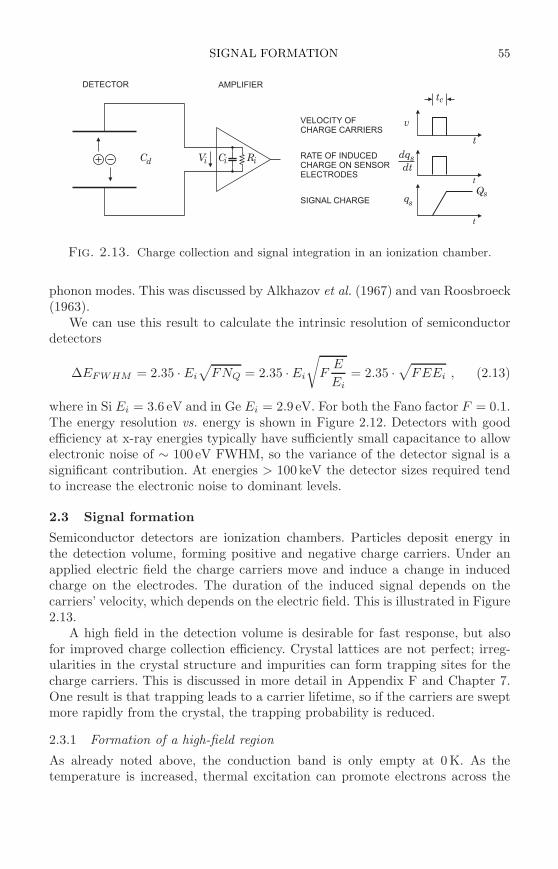
SIGNAL FORMATION 55
R
DETECTOR
CVC iid i
v
q
t
dq
Qs
c
s
s
t
t
t
dt
VELOCITY OF
CHARGE CARRIERS
RATE OF INDUCED
CHARGE ON SENSOR
ELECTRODES
SIGNAL CHARGE
AMPLIFIER
Fig. 2.13. Charge collection and signal integration in an ionization chamber.
phonon modes. This was discussed by Alkhazov et al. (1967) and van Roosbroeck(1963).
We can use this result to calculate the intrinsic resolution of semiconductordetectors
∆EFWHM = 2.35 · Ei
√
FNQ = 2.35 · Ei
√
FE
Ei= 2.35 ·
√
FEEi , (2.13)
where in Si Ei = 3.6 eV and in Ge Ei = 2.9 eV. For both the Fano factor F = 0.1.The energy resolution vs. energy is shown in Figure 2.12. Detectors with goodefficiency at x-ray energies typically have sufficiently small capacitance to allowelectronic noise of ∼ 100 eV FWHM, so the variance of the detector signal is asignificant contribution. At energies > 100 keV the detector sizes required tendto increase the electronic noise to dominant levels.
2.3 Signal formation
Semiconductor detectors are ionization chambers. Particles deposit energy inthe detection volume, forming positive and negative charge carriers. Under anapplied electric field the charge carriers move and induce a change in inducedcharge on the electrodes. The duration of the induced signal depends on thecarriers’ velocity, which depends on the electric field. This is illustrated in Figure2.13.
A high field in the detection volume is desirable for fast response, but alsofor improved charge collection efficiency. Crystal lattices are not perfect; irreg-ularities in the crystal structure and impurities can form trapping sites for thecharge carriers. This is discussed in more detail in Appendix F and Chapter 7.One result is that trapping leads to a carrier lifetime, so if the carriers are sweptmore rapidly from the crystal, the trapping probability is reduced.
2.3.1 Formation of a high-field region
As already noted above, the conduction band is only empty at 0 K. As thetemperature is increased, thermal excitation can promote electrons across the
56 SIGNAL FORMATION AND ACQUISITION
bandgap into the conduction band. In pure Si the carrier concentration is ∼1010 cm−3 at 300K, corresponding to a resistivity ρ ≈ 400 kΩ cm. Since the Silattice includes 5 · 1022 atoms/cm3, many states are available in the conductionband to allow carrier motion. In reality, crystal imperfections and minute impu-rity concentrations limit Si carrier concentrations to ∼ 1011 cm−3 at 300K, cor-responding to a resistivity ρ ≈ 40 kΩ cm. In practice, resistivities up to 20 kΩ cmare available, with mass production ranging from 5 to 10 kΩ cm.
As already noted in Chapter 1, these resistivities are too low for use in asimple crystal detector. However, a high-field region with low leakage current canbe established by using a reverse-biased pn-junction. The key to this technologyis the deliberate introduction of impurities to control the conductivity. Thisprocess is called doping.
2.3.2 Doping
The conductivity of semiconductors can be controlled by introducing specialimpurities. Required concentrations are in the range 1012 – 1018 cm−3, wherethe former is typical in radiation detectors. In semiconductors the conductivitycan be provided by either electrons (n-type) or holes (p-type).
2.3.2.1 n-type doping Replacing a silicon atom (group 4 in the periodic table,i.e. four valence electrons) by an atom with five valence electrons (e.g. P, As, Sb)leaves one valence electron without a partner (Figure 2.14). Since the impuritycontributes an excess electron to the lattice, it is called a donor.
The donor electron cannot be accommodated in the valence band, but it islightly bound to the impurity atom. As illustrated in Figure 2.15 the wavefunc-tion of the dopant atom extends over many neighbors, so one can, at least as anapproximation, utilize lattice properties such as the dielectric constant. Thus,the Coulomb force that binds the electron to the donor atom is reduced by the
SiSi
SiSi
SiSi
SiSi
SiSi
Si
Si
Si
P
Si
Si
Si
Si
ELECTRIC FIELD
PHOSPHORUS ATOM WITH
NET POSITIVE CHARGE
NUCLEUS WITH
CHARGE +5
EXCESS ELECTRON FROM PHOSPHORUS ATOM
Fig. 2.14. Introducing a group 5 impurity (e.g. P or As) introduces a lightly bound
electron that can move freely under the influence of an electric field. (Following
Shockley 1950.)
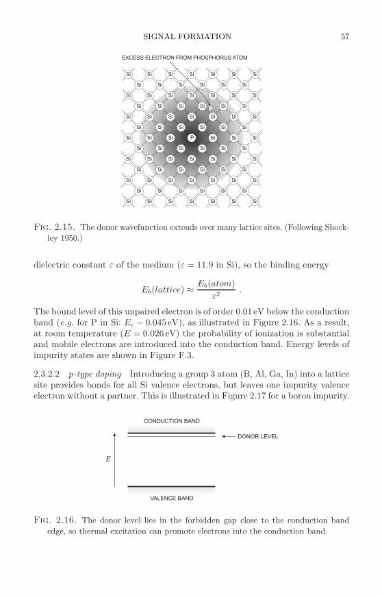
SIGNAL FORMATION 57
Si
Si
Si
Si
Si
Si
Si
Si
Si
Si
Si
Si
Si
Si
Si
Si
Si
Si
Si
Si
Si
Si
Si
Si
Si
Si
Si
Si
Si
Si
Si
Si
Si
Si
Si
Si
Si
Si
Si
Si
Si
Si
Si
Si
Si
Si
Si
Si
Si
Si
Si
Si
Si
Si
Si
Si
Si
Si
Si
Si
Si
Si
Si
Si
Si
Si
Si
Si
Si
Si
Si
Si
Si
Si
Si
Si
Si
Si
Si
Si
Si
Si
Si
Si
P
EXCESS ELECTRON FROM PHOSPHORUS ATOM
Fig. 2.15. The donor wavefunction extends over many lattice sites. (Following Shock-
ley 1950.)
dielectric constant ε of the medium (ε = 11.9 in Si), so the binding energy
Eb(lattice) ≈ Eb(atom)
ε2.
The bound level of this unpaired electron is of order 0.01 eV below the conductionband (e.g. for P in Si: Ec − 0.045 eV), as illustrated in Figure 2.16. As a result,at room temperature (E = 0.026 eV) the probability of ionization is substantialand mobile electrons are introduced into the conduction band. Energy levels ofimpurity states are shown in Figure F.3.
2.3.2.2 p-type doping Introducing a group 3 atom (B, Al, Ga, In) into a latticesite provides bonds for all Si valence electrons, but leaves one impurity valenceelectron without a partner. This is illustrated in Figure 2.17 for a boron impurity.
CONDUCTION BAND
VALENCE BAND
DONOR LEVEL
E
Fig. 2.16. The donor level lies in the forbidden gap close to the conduction band
edge, so thermal excitation can promote electrons into the conduction band.
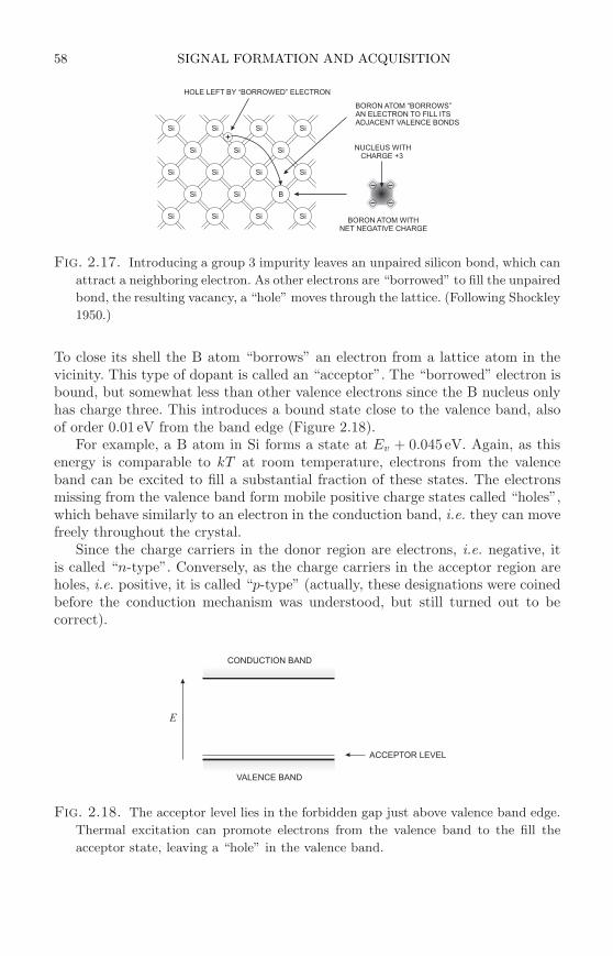
58 SIGNAL FORMATION AND ACQUISITION
SiSi
SiSi
SiSi
SiSi
SiSi
Si
Si
Si
B
Si
Si
Si
SiBORON ATOM WITH
NET NEGATIVE CHARGE
NUCLEUS WITH
CHARGE +3
HOLE LEFT BY “BORROWED” ELECTRON
BORON ATOM “BORROWS”
AN ELECTRON TO FILL ITS
ADJACENT VALENCE BONDS
Fig. 2.17. Introducing a group 3 impurity leaves an unpaired silicon bond, which can
attract a neighboring electron. As other electrons are “borrowed” to fill the unpaired
bond, the resulting vacancy, a “hole” moves through the lattice. (Following Shockley
1950.)
To close its shell the B atom “borrows” an electron from a lattice atom in thevicinity. This type of dopant is called an “acceptor”. The “borrowed” electron isbound, but somewhat less than other valence electrons since the B nucleus onlyhas charge three. This introduces a bound state close to the valence band, alsoof order 0.01 eV from the band edge (Figure 2.18).
For example, a B atom in Si forms a state at Ev + 0.045 eV. Again, as thisenergy is comparable to kT at room temperature, electrons from the valenceband can be excited to fill a substantial fraction of these states. The electronsmissing from the valence band form mobile positive charge states called “holes”,which behave similarly to an electron in the conduction band, i.e. they can movefreely throughout the crystal.
Since the charge carriers in the donor region are electrons, i.e. negative, itis called “n-type”. Conversely, as the charge carriers in the acceptor region areholes, i.e. positive, it is called “p-type” (actually, these designations were coinedbefore the conduction mechanism was understood, but still turned out to becorrect).
CONDUCTION BAND
VALENCE BAND
ACCEPTOR LEVEL
E
Fig. 2.18. The acceptor level lies in the forbidden gap just above valence band edge.
Thermal excitation can promote electrons from the valence band to the fill the
acceptor state, leaving a “hole” in the valence band.
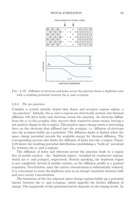
SIGNAL FORMATION 59
Fig. 2.19. Diffusion of electrons and holes across the junction forms a depletion zone
with a resulting potential between the p- and n-regions.
2.3.3 The pn-junction
Consider a crystal suitably doped that donor and acceptor regions adjoin, a“pn-junction”. Initially, the p- and n-regions are electrically neutral, but thermaldiffusion will drive holes and electrons across the junction. As electrons diffusefrom the n- to the p-region, they uncover their respective donor atoms, leaving anet positive charge in the n-region. This positive space charge exerts a restrainingforce on the electrons that diffused into the p-region, i.e. diffusion of electronsinto the p-region builds up a potential. The diffusion depth is limited when thespace charge potential exceeds the available energy for thermal diffusion. Thecorresponding process also limits the diffusion of holes into the n-region. Figure2.19 shows the resulting potential distribution establishing a “built-in” potentialVbi between the p- and n-regions.
The diffusion of holes and electrons across the junction leads to a regionfree of mobile carriers – the “depletion region”, bounded by conductive regions,which are n- and p-doped, respectively. Strictly speaking, the depletion regionis not completely devoid of mobile carriers, as the diffusion profile is a gradualtransition. Nevertheless, since the carrier concentration is substantially reduced,it is convenient to treat the depletion zone as an abrupt transition between bulkand zero carrier concentration.
The formation of the two adjacent space charge regions builds up a potentialbarrier between the n- and p-regions, which impedes the further diffusion ofcharge. The magnitude of this potential barrier depends on the doping levels. As
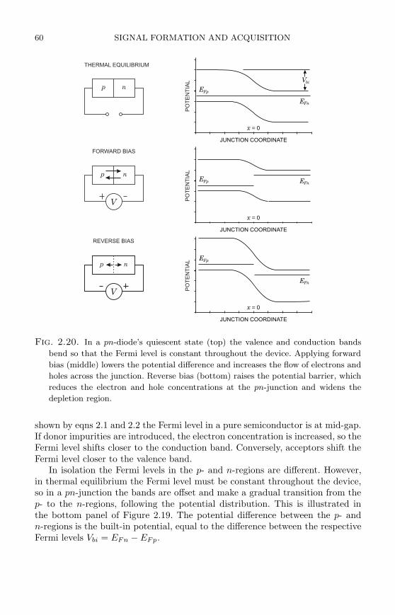
60 SIGNAL FORMATION AND ACQUISITION
p
p
p
n
n
n
V
V
THERMAL EQUILIBRIUM
FORWARD BIAS
REVERSE BIAS
JUNCTION COORDINATE
JUNCTION COORDINATE
JUNCTION COORDINATE
x = 0
x = 0
x = 0
E
E
E
Fp
Fp
Fp
E
E
E
Fn
Fn
Fn
Vbi
PO
TE
NT
IAL
PO
TE
NT
IAL
PO
TE
NT
IAL
Fig. 2.20. In a pn-diode’s quiescent state (top) the valence and conduction bands
bend so that the Fermi level is constant throughout the device. Applying forward
bias (middle) lowers the potential difference and increases the flow of electrons and
holes across the junction. Reverse bias (bottom) raises the potential barrier, which
reduces the electron and hole concentrations at the pn-junction and widens the
depletion region.
shown by eqns 2.1 and 2.2 the Fermi level in a pure semiconductor is at mid-gap.If donor impurities are introduced, the electron concentration is increased, so theFermi level shifts closer to the conduction band. Conversely, acceptors shift theFermi level closer to the valence band.
In isolation the Fermi levels in the p- and n-regions are different. However,in thermal equilibrium the Fermi level must be constant throughout the device,so in a pn-junction the bands are offset and make a gradual transition from thep- to the n-regions, following the potential distribution. This is illustrated inthe bottom panel of Figure 2.19. The potential difference between the p- andn-regions is the built-in potential, equal to the difference between the respectiveFermi levels Vbi = EFn − EFp.
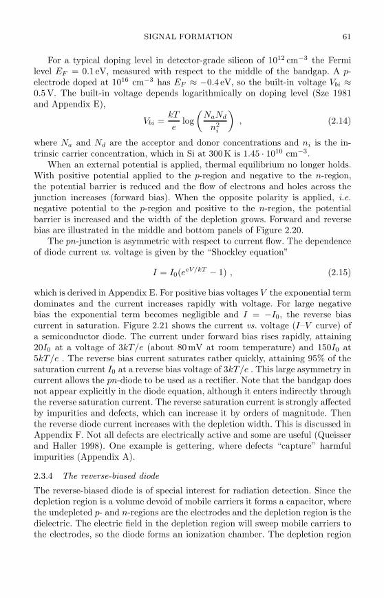
SIGNAL FORMATION 61
For a typical doping level in detector-grade silicon of 1012 cm−3 the Fermilevel EF = 0.1 eV, measured with respect to the middle of the bandgap. A p-electrode doped at 1016 cm−3 has EF ≈ −0.4 eV, so the built-in voltage Vbi ≈0.5V. The built-in voltage depends logarithmically on doping level (Sze 1981and Appendix E),
Vbi =kT
elog
(
NaNd
n2i
)
, (2.14)
where Na and Nd are the acceptor and donor concentrations and ni is the in-trinsic carrier concentration, which in Si at 300K is 1.45 · 1010 cm−3.
When an external potential is applied, thermal equilibrium no longer holds.With positive potential applied to the p-region and negative to the n-region,the potential barrier is reduced and the flow of electrons and holes across thejunction increases (forward bias). When the opposite polarity is applied, i.e.negative potential to the p-region and positive to the n-region, the potentialbarrier is increased and the width of the depletion grows. Forward and reversebias are illustrated in the middle and bottom panels of Figure 2.20.
The pn-junction is asymmetric with respect to current flow. The dependenceof diode current vs. voltage is given by the “Shockley equation”
I = I0(eeV/kT − 1) , (2.15)
which is derived in Appendix E. For positive bias voltages V the exponential termdominates and the current increases rapidly with voltage. For large negativebias the exponential term becomes negligible and I = −I0, the reverse biascurrent in saturation. Figure 2.21 shows the current vs. voltage (I–V curve) ofa semiconductor diode. The current under forward bias rises rapidly, attaining20I0 at a voltage of 3kT/e (about 80mV at room temperature) and 150I0 at5kT/e . The reverse bias current saturates rather quickly, attaining 95% of thesaturation current I0 at a reverse bias voltage of 3kT/e . This large asymmetry incurrent allows the pn-diode to be used as a rectifier. Note that the bandgap doesnot appear explicitly in the diode equation, although it enters indirectly throughthe reverse saturation current. The reverse saturation current is strongly affectedby impurities and defects, which can increase it by orders of magnitude. Thenthe reverse diode current increases with the depletion width. This is discussed inAppendix F. Not all defects are electrically active and some are useful (Queisserand Haller 1998). One example is gettering, where defects “capture” harmfulimpurities (Appendix A).
2.3.4 The reverse-biased diode
The reverse-biased diode is of special interest for radiation detection. Since thedepletion region is a volume devoid of mobile carriers it forms a capacitor, wherethe undepleted p- and n-regions are the electrodes and the depletion region is thedielectric. The electric field in the depletion region will sweep mobile carriers tothe electrodes, so the diode forms an ionization chamber. The depletion region
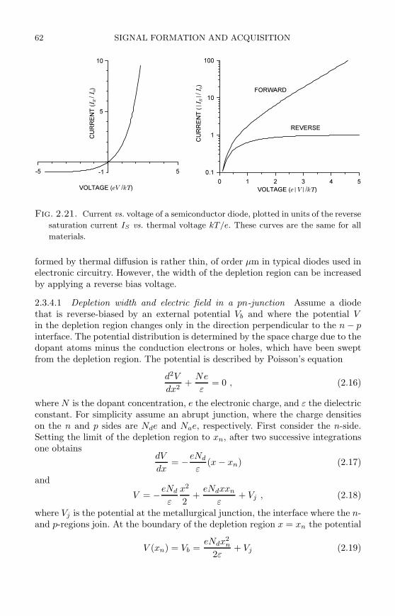
62 SIGNAL FORMATION AND ACQUISITION
-5 5
VOLTAGE (eV /kT)
CURRENT(I
R/I0)
0 1 2 3 4 5
VOLTAGE (e|V|/kT)
0.1
1
10
100
CURRENT(|IR|/I0)
10
5
-1
FORWARD
REVERSE
Fig. 2.21. Current vs. voltage of a semiconductor diode, plotted in units of the reverse
saturation current IS vs. thermal voltage kT/e. These curves are the same for all
materials.
formed by thermal diffusion is rather thin, of order µm in typical diodes used inelectronic circuitry. However, the width of the depletion region can be increasedby applying a reverse bias voltage.
2.3.4.1 Depletion width and electric field in a pn-junction Assume a diodethat is reverse-biased by an external potential Vb and where the potential Vin the depletion region changes only in the direction perpendicular to the n − pinterface. The potential distribution is determined by the space charge due to thedopant atoms minus the conduction electrons or holes, which have been sweptfrom the depletion region. The potential is described by Poisson’s equation
d2V
dx2+
Ne
ε= 0 , (2.16)
where N is the dopant concentration, e the electronic charge, and ε the dielectricconstant. For simplicity assume an abrupt junction, where the charge densitieson the n and p sides are Nde and Nae, respectively. First consider the n-side.Setting the limit of the depletion region to xn, after two successive integrationsone obtains
dV
dx= −eNd
ε(x − xn) (2.17)
and
V = −eNd
ε
x2
2+
eNdxxn
ε+ Vj , (2.18)
where Vj is the potential at the metallurgical junction, the interface where the n-and p-regions join. At the boundary of the depletion region x = xn the potential
V (xn) = Vb =eNdx
2n
2ε+ Vj (2.19)
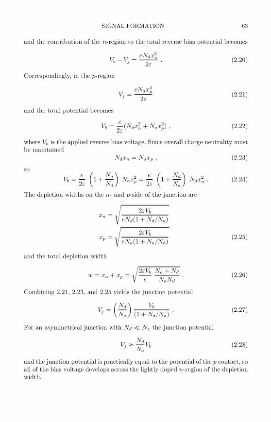
SIGNAL FORMATION 63
and the contribution of the n-region to the total reverse bias potential becomes
Vb − Vj =eNdx
2n
2ε. (2.20)
Correspondingly, in the p-region
Vj =eNax2
p
2ε(2.21)
and the total potential becomes
Vb =e
2ε(Ndx
2n + Nax2
p) , (2.22)
where Vb is the applied reverse bias voltage. Since overall charge neutrality mustbe maintained
Ndxn = Naxp , (2.23)
so
Vb =e
2ε
(
1 +Na
Nd
)
Nax2p =
e
2ε
(
1 +Nd
Na
)
Ndx2n . (2.24)
The depletion widths on the n- and p-side of the junction are
xn =
√
2εVb
eNd(1 + Nd/Na)
xp =
√
2εVb
eNa(1 + Na/Nd)(2.25)
and the total depletion width
w = xn + xp =
√
2εVb
e
Na + Nd
NaNd. (2.26)
Combining 2.21, 2.23, and 2.25 yields the junction potential
Vj =
(
Nd
Na
)
Vb
(1 + Nd/Na). (2.27)
For an asymmetrical junction with Nd ≪ Na the junction potential
Vj ≈ Nd
NaVb (2.28)
and the junction potential is practically equal to the potential of the p contact, soall of the bias voltage develops across the lightly doped n-region of the depletionwidth.

64 SIGNAL FORMATION AND ACQUISITION
300 m
~ 1 m
~ 1 m
GUARD RING
OHMIC CONTACT
JUNCTION CONTACTOXIDE
n Si BULK n DOPINGp DOPING ++
Fig. 2.22. Detector diodes are commonly formed by introducing a highly doped sur-
face layer into a lightly doped bulk. The depletion zone then extends into the bulk.
Metallization layers (black) provide electrical contacts to the doped p+ and n+
layers that form the junction and the back electrode (ohmic contact).
The depletion width increases with the square root of the reverse bias volt-age, so increasing the bias voltage will increase the sensitive volume and reducethe capacitance. For a charged particle traversing the detector this increases thesignal charge and reduces the electronic noise, so it is very beneficial. However,the maximum voltage one can apply is limited. At fields > 105 V/cm electronsacquire sufficient energy to form secondary electron–hole pairs, ultimately lead-ing to a destructive avalanche, called “breakdown”. This is discussed in moredetail in Section 2.8. Given this limit, the width of the depletion region can beincreased by reducing the dopant concentration. Ultimately, this is limited bythe minimum residual impurity levels in the crystal. In practice, lightly dopedsemiconductors include both donor and acceptor impurities and the net dopingis Nd − Na.
As already noted in Chapter 1, detector diodes are usually asymmetricallydoped, as shown in Figure 2.22. The starting material (bulk) is lightly dopedand the junction is formed by diffusing or ion-implanting a highly doped p+
layer into the n-type bulk. The depletion region then extends predominantlyinto the lightly doped bulk. The back contact is a highly doped layer of the sametype as the bulk, forming a nonrectifying “ohmic” contact.
In addition to the basic diode, Figure 2.22 shows a guard ring, which isolatesthe wafer edge (saw cut) from the active region. The guard ring is biased atthe same potential as the adjacent electrode, so the boundary of the detector’ssensitive volume is midway between the detector electrode and the guard ring. Inthe gap between the detector electrode and the guard ring it is critical to providea neutral interface at the silicon surface to prevent formation of a conductivepath, as discussed in Chapter 6. This is best accomplished by oxide passivation(SiO2, Appendix A).
When as discussed above Na ≫ Nd, the depletion region extends predomi-nantly into the n- side and the total depletion width is
w ≈ xn =
√
2εVb
eNd. (2.29)
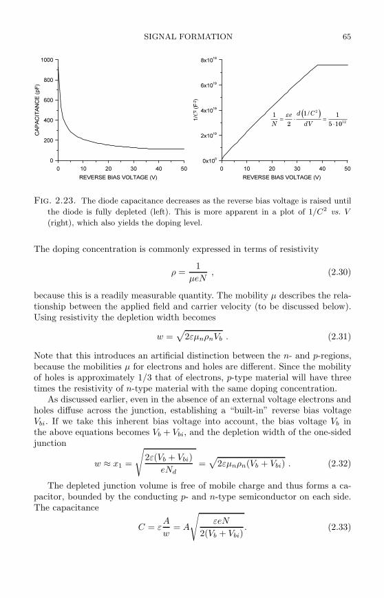
SIGNAL FORMATION 65
0 10 20 30 40 50
REVERSE BIAS VOLTAGE (V)
0
200
400
600
800
1000
CAPACITANCE(pF)
0 10 20 30 40 50
REVERSE BIAS VOLTAGE (V)
0x100
2x10¹⁹
4x10¹⁹
6x10¹⁹
8x10¹⁹
1/C
2(F
-2)
( )2
12
1 /1 1
2 5 10
d Ce
N dV
ε
= ⋅ =
⋅
Fig. 2.23. The diode capacitance decreases as the reverse bias voltage is raised until
the diode is fully depleted (left). This is more apparent in a plot of 1/C2 vs. V
(right), which also yields the doping level.
The doping concentration is commonly expressed in terms of resistivity
ρ =1
µeN, (2.30)
because this is a readily measurable quantity. The mobility µ describes the rela-tionship between the applied field and carrier velocity (to be discussed below).Using resistivity the depletion width becomes
w =√
2εµnρnVb . (2.31)
Note that this introduces an artificial distinction between the n- and p-regions,because the mobilities µ for electrons and holes are different. Since the mobilityof holes is approximately 1/3 that of electrons, p-type material will have threetimes the resistivity of n-type material with the same doping concentration.
As discussed earlier, even in the absence of an external voltage electrons andholes diffuse across the junction, establishing a “built-in” reverse bias voltageVbi. If we take this inherent bias voltage into account, the bias voltage Vb inthe above equations becomes Vb + Vbi, and the depletion width of the one-sidedjunction
w ≈ x1 =
√
2ε(Vb + Vbi)
eNd=√
2εµnρn(Vb + Vbi) . (2.32)
The depleted junction volume is free of mobile charge and thus forms a ca-pacitor, bounded by the conducting p- and n-type semiconductor on each side.The capacitance
C = εA
w= A
√
εeN
2(Vb + Vbi). (2.33)
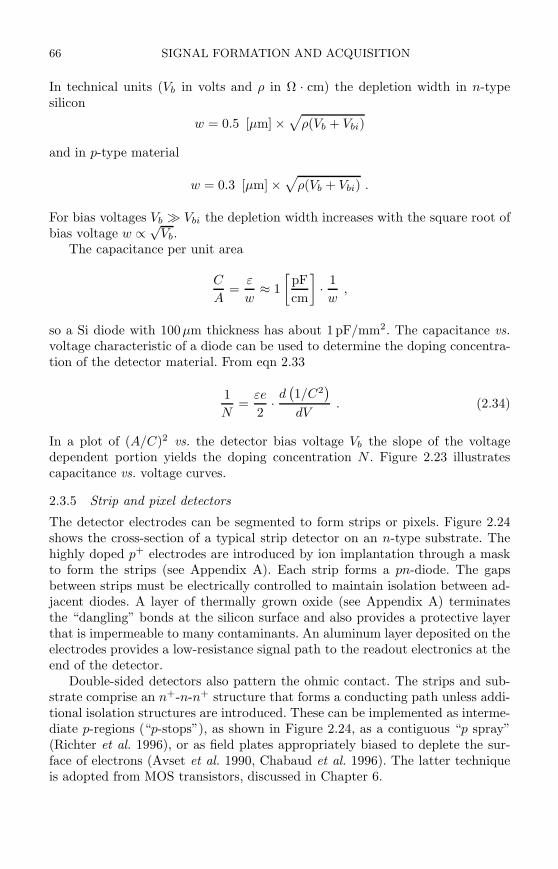
66 SIGNAL FORMATION AND ACQUISITION
In technical units (Vb in volts and ρ in Ω · cm) the depletion width in n-typesilicon
w = 0.5 [µm] ×√
ρ(Vb + Vbi)
and in p-type material
w = 0.3 [µm] ×√
ρ(Vb + Vbi) .
For bias voltages Vb ≫ Vbi the depletion width increases with the square root ofbias voltage w ∝ √
Vb.The capacitance per unit area
C
A=
ε
w≈ 1
[
pF
cm
]
· 1
w,
so a Si diode with 100µm thickness has about 1 pF/mm2. The capacitance vs.voltage characteristic of a diode can be used to determine the doping concentra-tion of the detector material. From eqn 2.33
1
N=
εe
2· d(
1/C2)
dV. (2.34)
In a plot of (A/C)2 vs. the detector bias voltage Vb the slope of the voltagedependent portion yields the doping concentration N . Figure 2.23 illustratescapacitance vs. voltage curves.
2.3.5 Strip and pixel detectors
The detector electrodes can be segmented to form strips or pixels. Figure 2.24shows the cross-section of a typical strip detector on an n-type substrate. Thehighly doped p+ electrodes are introduced by ion implantation through a maskto form the strips (see Appendix A). Each strip forms a pn-diode. The gapsbetween strips must be electrically controlled to maintain isolation between ad-jacent diodes. A layer of thermally grown oxide (see Appendix A) terminatesthe “dangling” bonds at the silicon surface and also provides a protective layerthat is impermeable to many contaminants. An aluminum layer deposited on theelectrodes provides a low-resistance signal path to the readout electronics at theend of the detector.
Double-sided detectors also pattern the ohmic contact. The strips and sub-strate comprise an n+-n-n+ structure that forms a conducting path unless addi-tional isolation structures are introduced. These can be implemented as interme-diate p-regions (“p-stops”), as shown in Figure 2.24, as a contiguous “p spray”(Richter et al. 1996), or as field plates appropriately biased to deplete the sur-face of electrons (Avset et al. 1990, Chabaud et al. 1996). The latter techniqueis adopted from MOS transistors, discussed in Chapter 6.
CHARGE COLLECTION 67
p n-on- STRIPS n n-on- STRIPS
p-STRIP n-STRIP
n-SILICON n-SILICON
Al CONTACT STRIP INTERMEDIATE STRIPp-
PSG
SiO SURFACE
PASSIVATION
OHMIC CONTACT
2
Fig. 2.24. Cross-section of the electrode structure in strip detectors. The left shows
the junction side of a single-sided detector. In double-sided detectors the electrodes
on the ohmic side require additional isolation structures, for example an intermedi-
ate p-region as shown at the right. A layer of phosphosilicate glass (PSG) protects
the structure.
2.4 Charge collection
Carrier transport can proceed through diffusion or drift. Diffusion is driven bya concentration gradient. Thermal energy causes carriers to move in randomdirections, but in the presence of a concentration gradient they collide morefrequently in the direction of higher concentration, so the net motion is in theopposite direction. The concentration profile spreads out with time forming aGaussian distribution with the variance
σ =√
Dt , (2.35)
where D is a material-dependent diffusion constant.In the presence of an electric field, the carriers move parallel to the field
(drift). However, the velocity does not depend on the time during which thecharge carrier is accelerated, as in normal ballistic motion, since the charge carrieralso interacts with the crystal lattice, exciting lattice vibrations (phonons). Thecharacteristic times for phonon excitation are much smaller than the transporttimes, so the carrier is always in equilibrium with the lattice and the velocity isonly a function of the electric field
v = µE , (2.36)
where µ is the mobility. The mobility is linked to the diffusion constant throughthe Einstein relation
µ =e
kTD . (2.37)
68 SIGNAL FORMATION AND ACQUISITION
V< V V>Vd d
w d d
E
E
Emax
max
min
x x
E E
Fig. 2.25. Electric field in a reverse-biased diode in partial depletion (left) and with
overbias (right)
Electrons and holes have different mobilities, 1350 and 450 cm2/Vs in Si, re-spectively (Beadle, Tsai, and Plummer 1984). Thus, in a field of 103 V/cm theelectron velocity is 1.35 · 106 cm/s. For comparison, the thermal velocity of anelectron in Si at room temperature is about 107 cm/s, so the carrier motion isthe superposition of a substantial random thermal motion and the drift due tothe electric field.
Radiation absorbed in the detector’s sensitive region forms mobile electronsand holes, which move under the influence of the electric field. Although electronsand holes move in opposite directions, their contribution to the signal currentis of the same polarity since they have opposite charge. The time required for acharge carrier to traverse the sensitive volume is called the collection time.
Using the depletion width eqn 2.25 one can rewrite eqn 2.17 for the electricfield
E(x) =2(Vb + Vbi)
w
( x
w− 1)
. (2.38)
The detector bulk is completely depleted of mobile charge when the depletionwidth equals the thickness of the detector W = d. This occurs at the externallyapplied depletion voltage
Vd =eNdw
2
2ε− Vbi . (2.39)
The field drops linearly from its maximum value at the junction to zero at theopposite contact. Increasing the bias voltage beyond this value adds a uniformfield due to the voltage beyond depletion, yielding a distribution
E(x) =2Vdi
d
(
1 − x
d
)
+Vb − Vdi
d, (2.40)
where Vdi ≡ Vd + Vbi has been defined as the internal depletion voltage. Figure2.25 shows the field distribution in partial depletion and with overbias.
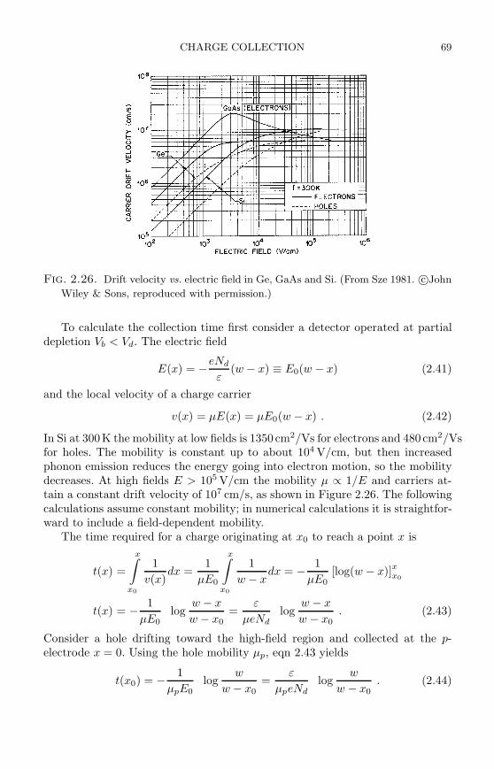
CHARGE COLLECTION 69
Fig. 2.26. Drift velocity vs. electric field in Ge, GaAs and Si. (From Sze 1981. c©John
Wiley & Sons, reproduced with permission.)
To calculate the collection time first consider a detector operated at partialdepletion Vb < Vd. The electric field
E(x) = −eNd
ε(w − x) ≡ E0(w − x) (2.41)
and the local velocity of a charge carrier
v(x) = µE(x) = µE0(w − x) . (2.42)
In Si at 300K the mobility at low fields is 1350 cm2/Vs for electrons and 480 cm2/Vsfor holes. The mobility is constant up to about 104 V/cm, but then increasedphonon emission reduces the energy going into electron motion, so the mobilitydecreases. At high fields E > 105 V/cm the mobility µ ∝ 1/E and carriers at-tain a constant drift velocity of 107 cm/s, as shown in Figure 2.26. The followingcalculations assume constant mobility; in numerical calculations it is straightfor-ward to include a field-dependent mobility.
The time required for a charge originating at x0 to reach a point x is
t(x) =
x∫
x0
1
v(x)dx =
1
µE0
x∫
x0
1
w − xdx = − 1
µE0[log(w − x)]
xx0
t(x) = − 1
µE0log
w − x
w − x0=
ε
µeNdlog
w − x
w − x0. (2.43)
Consider a hole drifting toward the high-field region and collected at the p-electrode x = 0. Using the hole mobility µp, eqn 2.43 yields
t(x0) = − 1
µpE0log
w
w − x0=
ε
µpeNdlog
w
w − x0. (2.44)
70 SIGNAL FORMATION AND ACQUISITION
If we define a characteristic collection time
τp ≡ ε
µpeNd, (2.45)
then
t(x0) = τp logw
w − x0. (2.46)
For example, t(x0 = 0.5w) = 0.7τp and t(x0 = 0.95w) = 3.0τp.For the electrons drifting toward the low-field electrode x = w, eqn 2.43
does not yield a solution. However, it can be rewritten to yield the position as afunction of time
x(t) = w − (w − x0) e−t/ τn , (2.47)
where τn has been defined analogously to τp. For a charge originating at themetallurgical junction x0 = 0 and drifting toward x = w
x(t) = w(1 − e−t/ τn) . (2.48)
In this simple picture, a charge carrier drifting toward the low-field regionis never collected (in reality this is accomplished by diffusion), although after atime t = 3τn the carrier will have traversed 95% of the detector. Note that in apartially depleted detector the collection time constants τn and τp are indepen-dent of the applied bias voltage (and depletion thickness), but determined onlyby the doping concentration of the bulk material and the carrier mobility. τn isnumerically equal to the dielectric relaxation time of the n-type bulk
τ = ρε = εSi ε0 ρ = 1.05[ ns
kΩ · cm]
ρ ,
so the resistivity gives a quick estimate of the collection time. In n-type silicon of10 kΩ cm resistivity τn = 10.5ns and τp = 31.5ns, so collection times are about30 and 90ns, respectively.
The collection time can be reduced by operating the detector at bias voltagesexceeding the depletion voltage (overbias, often referred to as “overdepletion”).The field distribution was given in eqn 2.40, which can be rewritten as
E(x) = E0
(
1 − x
d
)
+ E1 . (2.49)
This yields a collection time
t(x) =
x∫
x0
1
v(x)dx =
1
µ
x∫
x0
1
E0
(
1 − x
d
)
+ E1
dx = − d
µE0
[
log(
E0 + E1 − E0x
d
)]x
x0
TIME DEPENDENCE OF THE SIGNAL CURRENT 71
t(x) =d
µE0log
E0 + E1 − E0x
d
E0 + E1 − E0x0
d
. (2.50)
For holes originating at x0 = w and drifting to the p-electrode x = 0
tcp =d
µpE0log
(
1 +E0
E1
)
. (2.51)
The corresponding result obtains for electrons originating at x0 = 0 and driftingto the n-electrode x = w
tcn =d
µnE0log
(
1 +E0
E1
)
. (2.52)
For large overbias E1 ≫ E0,
log
(
1 +E0
E1
)
≈ E0
E1(2.53)
and
tcp =d
µpE1, (2.54)
as expected for a uniform field.Rewritten in terms of voltages, eqns 2.52 and 2.53 become
tcp =d2
2µpVdilog
(
Vb + Vdi
Vb − Vdi
)
(2.55)
and
tcn =d2
2µnVdilog
(
Vb + Vdi
Vb − Vdi
)
, (2.56)
where Vdi ≡ Vd + Vbi .For example, consider a sensor made of n-type silicon with 10kΩ cm resistivity
and a thickness of 300µm. The depletion voltage is 30V. When operated attwice the depletion voltage Vb = 60V (i.e. E0 = 2 ·103 and E1 = 103 V/cm), thecollection times are 12ns for electrons and 36ns for holes. These are substantiallysmaller than in the partially depleted device, where collection times are 30ns forelectrons and 90ns for holes.
2.5 Time dependence of the signal current
As illustrated in Figure 2.27, charge moving in the sensitive volume of the sensorgives rise to a signal current, as indicated in the accompanying equivalent circuit.At this point we need to determine is(t). When does the signal current begin?When the charge reaches the electrode or when the charge begins to move?
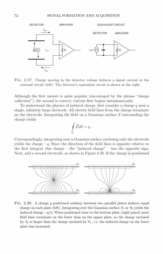
72 SIGNAL FORMATION AND ACQUISITION
Cd
AMPLIFIER
i
i
sig
sig
i (t)s RR ii
DETECTOR
DETECTOR AMPLIFIER EQUIVALENT CIRCUIT
Fig. 2.27. Charge moving in the detector volume induces a signal current in the
external circuit (left). The detector’s equivalent circuit is shown at the right.
Although the first answer is quite popular (encouraged by the phrase “chargecollection”), the second is correct; current flow begins instantaneously.
To understand the physics of induced charge, first consider a charge q near asingle, infinitely large electrode. All electric field lines from the charge terminateon the electrode. Integrating the field on a Gaussian surface S surrounding thecharge yields
∮
S
Eda = q .
Correspondingly, integrating over a Gaussian surface enclosing only the electrodeyields the charge −q. Since the direction of the field lines is opposite relative tothe first integral, this charge – the “induced charge” – has the opposite sign.Next, add a second electrode, as shown in Figure 2.28. If the charge is positioned
S
S
1
2
S
S
1
2
Fig. 2.28. A charge q positioned midway between two parallel plates induces equal
charge on each plate (left). Integrating over the Gaussian surface S1 or S2 yields the
induced charge −q/2. When positioned close to the bottom plate (right panel) more
field lines terminate on the lower than on the upper plate, so the charge enclosed
by S2 is larger than the charge enclosed by S1, i.e. the induced charge on the lower
plate has increased.
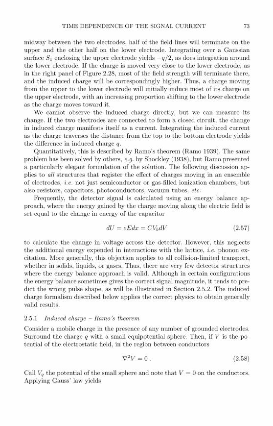
TIME DEPENDENCE OF THE SIGNAL CURRENT 73
midway between the two electrodes, half of the field lines will terminate on theupper and the other half on the lower electrode. Integrating over a Gaussiansurface S1 enclosing the upper electrode yields −q/2, as does integration aroundthe lower electrode. If the charge is moved very close to the lower electrode, asin the right panel of Figure 2.28, most of the field strength will terminate there,and the induced charge will be correspondingly higher. Thus, a charge movingfrom the upper to the lower electrode will initially induce most of its charge onthe upper electrode, with an increasing proportion shifting to the lower electrodeas the charge moves toward it.
We cannot observe the induced charge directly, but we can measure itschange. If the two electrodes are connected to form a closed circuit, the changein induced charge manifests itself as a current. Integrating the induced currentas the charge traverses the distance from the top to the bottom electrode yieldsthe difference in induced charge q.
Quantitatively, this is described by Ramo’s theorem (Ramo 1939). The sameproblem has been solved by others, e.g. by Shockley (1938), but Ramo presenteda particularly elegant formulation of the solution. The following discussion ap-plies to all structures that register the effect of charges moving in an ensembleof electrodes, i.e. not just semiconductor or gas-filled ionization chambers, butalso resistors, capacitors, photoconductors, vacuum tubes, etc.
Frequently, the detector signal is calculated using an energy balance ap-proach, where the energy gained by the charge moving along the electric field isset equal to the change in energy of the capacitor
dU = eEdx = CVbdV (2.57)
to calculate the change in voltage across the detector. However, this neglectsthe additional energy expended in interactions with the lattice, i.e. phonon ex-citation. More generally, this objection applies to all collision-limited transport,whether in solids, liquids, or gases. Thus, there are very few detector structureswhere the energy balance approach is valid. Although in certain configurationsthe energy balance sometimes gives the correct signal magnitude, it tends to pre-dict the wrong pulse shape, as will be illustrated in Section 2.5.2. The inducedcharge formalism described below applies the correct physics to obtain generallyvalid results.
2.5.1 Induced charge – Ramo’s theorem
Consider a mobile charge in the presence of any number of grounded electrodes.Surround the charge q with a small equipotential sphere. Then, if V is the po-tential of the electrostatic field, in the region between conductors
∇2V = 0 . (2.58)
Call Vq the potential of the small sphere and note that V = 0 on the conductors.Applying Gauss’ law yields

74 SIGNAL FORMATION AND ACQUISITION
∫
sphere′ssurface
∂V
∂nds = 4πq . (2.59)
Next, consider the charge removed and one conductor A raised to unit potential.Call the potential V1, so that
∇2V1 = 0 (2.60)
in the space between the conductors, including the site where the charge wassituated. Call the new potential at this point Vq1. Green’s theorem states that
∫
volumebetweenboundaries
(V1∇2V − V ∇2V1)dv = −∫
boundarysurfaces
[
V1∂V
∂n− V
∂V1
∂n
]
ds . (2.61)
Choose the volume to be bounded by the conductors and the tiny sphere. Thenthe left-hand side is 0 and the right-hand side may be divided into three integrals:
1. Over the surfaces of all conductors except A. This integral is 0 since onthese surfaces V = V1 = 0.
2. Over the surface of A. As V1 = 1 and V = 0 this reduces to
−∫
surfaceA
∂V
∂nds
3. Over the surface of the sphere.
−Vq1
∫
sphere′ssurface
∂V
∂nds + Vq
∫
sphere′ssurface
∂V1
∂nds
The second integral is zero by Gauss’ law, since in this case the charge is removed.Combining these three integrals yields
0 = −∫
surfaceA
∂V
∂nds − Vq1
∫
sphere′ssurface
∂V
∂nds = 4πQA − 4πqVq1 (2.62)
orQA = qVq1 . (2.63)
If the charge q moves in direction x, the current on electrode A is
iA =dQA
dt= q
dVq1
dt= q
(
∂Vq1
∂x
dx
dt
)
. (2.64)
Since the charge’s velocity
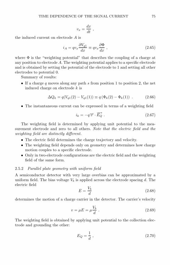
TIME DEPENDENCE OF THE SIGNAL CURRENT 75
vx =dx
dt,
the induced current on electrode A is
iA = qvx∂Vq1
dx≡ qvx
∂Φ
dx, (2.65)
where Φ is the “weighting potential” that describes the coupling of a charge atany position to electrode A. The weighting potential applies to a specific electrodeand is obtained by setting the potential of the electrode to 1 and setting all otherelectrodes to potential 0.
Summary of results:
• If a charge q moves along any path s from position 1 to position 2, the netinduced charge on electrode k is
∆Qk = q(Vq1(2) − Vq1(1)) ≡ q (Φk(2) − Φk(1)) . (2.66)
• The instantaneous current can be expressed in terms of a weighting field
ik = −q−→v · −→EQ . (2.67)
The weighting field is determined by applying unit potential to the mea-surement electrode and zero to all others. Note that the electric field and theweighting field are distinctly different.
• The electric field determines the charge trajectory and velocity.
• The weighting field depends only on geometry and determines how chargemotion couples to a specific electrode.
• Only in two-electrode configurations are the electric field and the weightingfield of the same form.
2.5.2 Parallel plate geometry with uniform field
A semiconductor detector with very large overbias can be approximated by auniform field. The bias voltage Vb is applied across the electrode spacing d. Theelectric field
E =Vb
d(2.68)
determines the motion of a charge carrier in the detector. The carrier’s velocity
v = µE = µVb
d. (2.69)
The weighting field is obtained by applying unit potential to the collection elec-trode and grounding the other:
EQ =1
d, (2.70)
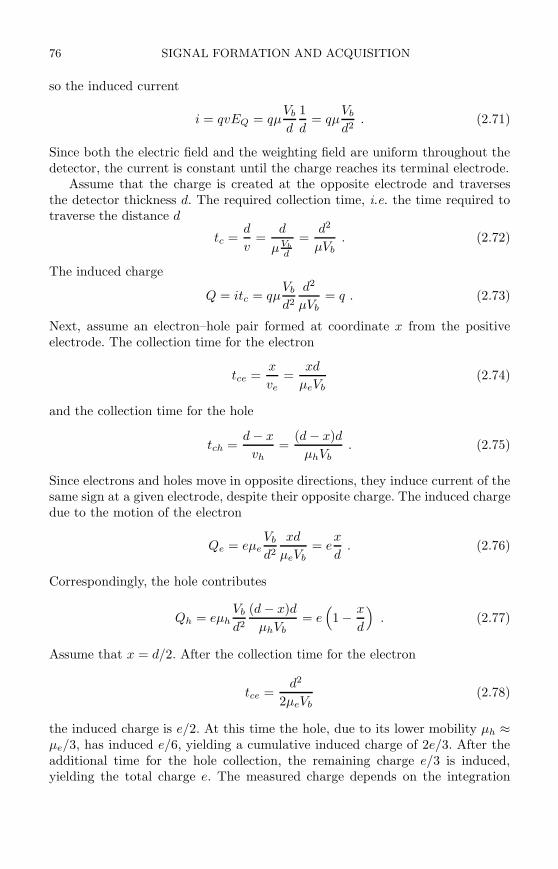
76 SIGNAL FORMATION AND ACQUISITION
so the induced current
i = qvEQ = qµVb
d
1
d= qµ
Vb
d2. (2.71)
Since both the electric field and the weighting field are uniform throughout thedetector, the current is constant until the charge reaches its terminal electrode.
Assume that the charge is created at the opposite electrode and traversesthe detector thickness d. The required collection time, i.e. the time required totraverse the distance d
tc =d
v=
d
µVb
d
=d2
µVb. (2.72)
The induced charge
Q = itc = qµVb
d2
d2
µVb= q . (2.73)
Next, assume an electron–hole pair formed at coordinate x from the positiveelectrode. The collection time for the electron
tce =x
ve=
xd
µeVb(2.74)
and the collection time for the hole
tch =d − x
vh=
(d − x)d
µhVb. (2.75)
Since electrons and holes move in opposite directions, they induce current of thesame sign at a given electrode, despite their opposite charge. The induced chargedue to the motion of the electron
Qe = eµeVb
d2
xd
µeVb= e
x
d. (2.76)
Correspondingly, the hole contributes
Qh = eµhVb
d2
(d − x)d
µhVb= e
(
1− x
d
)
. (2.77)
Assume that x = d/2. After the collection time for the electron
tce =d2
2µeVb(2.78)
the induced charge is e/2. At this time the hole, due to its lower mobility µh ≈µe/3, has induced e/6, yielding a cumulative induced charge of 2e/3. After theadditional time for the hole collection, the remaining charge e/3 is induced,yielding the total charge e. The measured charge depends on the integration
TIME DEPENDENCE OF THE SIGNAL CURRENT 77
time. Integration times larger than the collection time of all charge carriers yieldthe full charge. A shorter integration time yields a fractional charge.
Equation 2.76 illustrates the difference between the induced charge and theerroneous energy balance approach, which predicts the incremental signal chargedQ = e dV/V instead of dQ = e dx/d. Superficially, it appears that the energybalance gives a different result because the potential distribution in a parallelplate semiconductor detector is not linear due to space charge. However, asdiscussed by Cavalleri et al. (1972) the validity of Ramo’s theorem is not affectedby the presence of space charge. Fundamentally, the discrepancy arises becausewe are not dealing with ballistic transport and the energy balance approachinvokes a conservation law without considering the total energy of the system.
In the parallel plate configuration electrons and holes contribute equally tothe currents on both electrodes and the instantaneous current at any time isthe same on both electrodes, although of opposite sign. The continuity equation(Kirchhoff’s law) must be satisfied:
∑
k
ik = 0 . (2.79)
With only two electrodes, i1 = −i2 and the currents observed on the n and pelectrodes differ only in their polarity. In the presence of multiple electrodes theinstantaneous current from one electrode must balance the sum of the currentsfrom the others, so all signal currents can be different. This is the situation instrip detectors.
Fig. 2.29. Weighting potential for a 300 µm thick strip detector with strips on a
pitch of 50 µm. The central strip is at unit potential and the others at zero. Only
50 µm of depth are shown.
78 SIGNAL FORMATION AND ACQUISITION
2.5.3 Double-sided strip detector
The detector has strip electrodes on both faces. The strip pitch is assumed to besmall compared to the thickness. The electric field is similar to a parallel-plategeometry, except in the immediate vicinity of the strips. The signal weightingpotential, however is very different, as shown in Figure 2.29.
Figure 2.30 shows cuts through the weighting potential and the weightingfield along the center of the signal strip (left) and the neighbor strip (right).Consider an electron–hole pair qn, qp originating at a point x0 on the center-lineof a strip. The motion of the electron towards the n-electrode at coordinate xn
is equivalent to the motion of a hole in the opposite direction to the p-electrodeat xp. The total induced charge on electrode k after the charges have traversedthe detector is
0 50 100 150 200 250 300
DEPTH IN DETECTOR (µm)
0
0.2
0.4
0.6
0.8
1
WEIG
HTING
POTENTIAL
SIGNAL STRIP
0 50 100 150 200 250 300
DEPTH IN DETECTOR (µm)
0
0.04
0.08
0.12
0.16
WEIG
HTING
POTENTIAL
NEIGHBOR STRIP
0 50 100 150 200 250 300
DEPTH IN DETECTOR (µm)
-0.06
-0.04
-0.02
0
WEIG
HTING
FIELD SIGNAL STRIP
0 50 100 150 200 250 300
DEPTH IN DETECTOR (µm)
-0.004
0
0.004
0.008
0.012
0.016
WEIG
HTING
FIELD NEIGHBOR STRIP
Fig. 2.30. Cuts of the weighting field through the center of a strip electrode and
through the neighboring electrode. Along the axis of a measurement electrode the
weighting field is monotonic, so the signal charge increases as the carrier approaches
the electrode. The weighting field through the neighbor electrode changes sign at
about 40 µm depth, so the induced current inverts and the signal on this strip
integrates to zero.

TIME DEPENDENCE OF THE SIGNAL CURRENT 79
Qk = qp[ΦQk(xp) − ΦQk(x0)] + qn[ΦQk(xn) − ΦQk(x0)] . (2.80)
Since the hole charge qp = e and qn = −e,
Qk = e[ΦQk(xp) − ΦQk(x0)] − e[ΦQk(xn) − ΦQk(x0)] . (2.81)
If the signal is measured on the p-electrode, collecting the holes,
Qk = e[ΦQk(xp) − ΦQk(xn)] . (2.82)
Then ΦQk(xp) = 1, ΦQk(xn) = 0, and Qk = e. If, however, the charge is collectedon the neighboring strip k+1, then ΦQk+1(xp) = 0, ΦQk+1(xn) = 0, and Qk+1 =0.
In general, if a moving charge does not terminate on the measurement elec-trode, signal current will be induced, but the current changes sign and integratesto zero. This is illustrated in Figure 2.31. The plots of the weighting field in Fig-ure 2.30 show that the induced current on both the signal and neighbor strips isstrongly peaked near the strip. However, the weighting field of the neighbor stripchanges sign at about 40µm distance from the strip electrode, so the inducedcharge initially builds up as a carrier drifts 260µm from the far side and thenrapidly reduces to zero as the carrier reaches the signal strip.
Fig. 2.31. The weighting field in a strip detector. The measurement electrode is
the right-most strip. The induced current is shown for a charge terminating on
the measurement electrode (right) and the neighbor electrode (left), showing the
change in polarity. (From Radeka 1988. c©Annual Reviews www.annualreviews.org,
reprinted with permission)
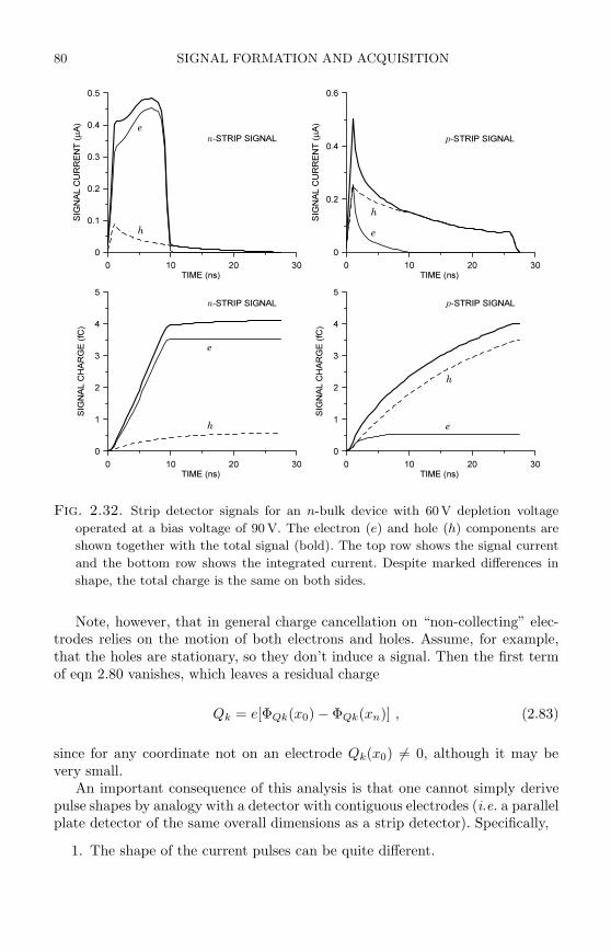
80 SIGNAL FORMATION AND ACQUISITION
0 10 20 30TIME (ns)
0
0.1
0.2
0.3
0.4
0.5
SIG
NALCURRENT(µA)
0 10 20 30TIME (ns)
0
0.2
0.4
0.6
SIG
NALCURRENT(µA)
0 10 20 30TIME (ns)
0
1
2
3
4
5
SIG
NALCHARGE(fC)
0 10 20 30TIME (ns)
0
1
2
3
4
5
SIG
NALCHARGE(fC)
n-STRIP SIGNAL p-STRIP SIGNAL
n-STRIP SIGNAL p-STRIP SIGNAL
e
h e
h
e
eh
h
Fig. 2.32. Strip detector signals for an n-bulk device with 60 V depletion voltage
operated at a bias voltage of 90 V. The electron (e) and hole (h) components are
shown together with the total signal (bold). The top row shows the signal current
and the bottom row shows the integrated current. Despite marked differences in
shape, the total charge is the same on both sides.
Note, however, that in general charge cancellation on “non-collecting” elec-trodes relies on the motion of both electrons and holes. Assume, for example,that the holes are stationary, so they don’t induce a signal. Then the first termof eqn 2.80 vanishes, which leaves a residual charge
Qk = e[ΦQk(x0) − ΦQk(xn)] , (2.83)
since for any coordinate not on an electrode Qk(x0) = 0, although it may bevery small.
An important consequence of this analysis is that one cannot simply derivepulse shapes by analogy with a detector with contiguous electrodes (i.e. a parallelplate detector of the same overall dimensions as a strip detector). Specifically,
1. The shape of the current pulses can be quite different.
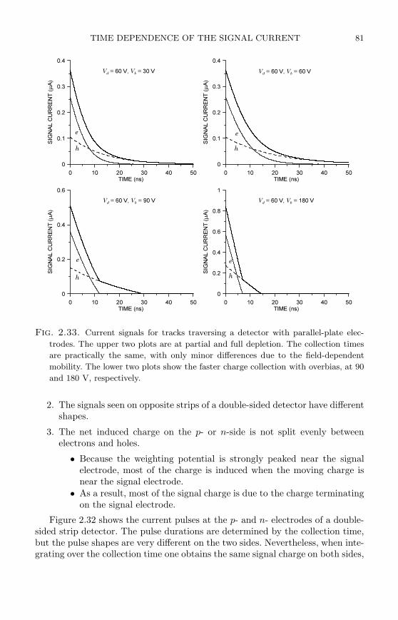
TIME DEPENDENCE OF THE SIGNAL CURRENT 81
0 10 20 30 40 50TIME (ns)
0
0.1
0.2
0.3
0.4
SIG
NALCURRENT(µA)
0 10 20 30 40 50TIME (ns)
0
0.1
0.2
0.3
0.4
SIG
NALCURRENT(µA)
0 10 20 30 40 50TIME (ns)
0
0.2
0.4
0.6
SIG
NALCURRENT(µA)
0 10 20 30 40 50TIME (ns)
0
0.2
0.4
0.6
0.8
1
SIG
NALCURRENT(µA)
Vd
= 60 V, Vb
= 30 V Vd
= 60 V, Vb
= 60 V
Vd
= 60 V, Vb
= 90 V Vd
= 60 V, Vb
= 180 V
e
h
e
h
e e
h h
Fig. 2.33. Current signals for tracks traversing a detector with parallel-plate elec-
trodes. The upper two plots are at partial and full depletion. The collection times
are practically the same, with only minor differences due to the field-dependent
mobility. The lower two plots show the faster charge collection with overbias, at 90
and 180 V, respectively.
2. The signals seen on opposite strips of a double-sided detector have differentshapes.
3. The net induced charge on the p- or n-side is not split evenly betweenelectrons and holes.
• Because the weighting potential is strongly peaked near the signalelectrode, most of the charge is induced when the moving charge isnear the signal electrode.
• As a result, most of the signal charge is due to the charge terminatingon the signal electrode.
Figure 2.32 shows the current pulses at the p- and n- electrodes of a double-sided strip detector. The pulse durations are determined by the collection time,but the pulse shapes are very different on the two sides. Nevertheless, when inte-grating over the collection time one obtains the same signal charge on both sides,
82 SIGNAL FORMATION AND ACQUISITION
as also shown in Figure 2.32. Since the weighting function is so strongly peakednear the strip electrodes, nearly all of the signal charge on the n-side is dueto electrons and on the p-side due to holes. For comparison, Figure 2.33 showsthe signal currents of a detector with a simple parallel-plate electrode structureand the same depletion voltage. The pulse shapes are strikingly different fromthose shown for a strip detector. At partial and full depletion the pulse shapesare practically unchanged, except for minor differences due to the field depen-dent mobility. The speed-up in charge collection with overbias is also apparent.Overbias also removes the drawn-out “tails” due to the vanishing field as carriersapproach the ohmic electrode. For the same depletion and bias voltages the pulsedurations are the same as in strip detectors, but the shapes of the current differgreatly because of the different weighting field.
2.6 Charge collection in the presence of trapping
Practical semiconductor crystals suffer from imperfections introduced duringcrystal growth, during device fabrication, or by radiation damage. Defects inthe crystal such as impurity atoms, vacancies, and structural irregularities (e.g.dislocations) introduce states into the crystal that can trap charge.
Extremely minute trap concentrations lead to significant effects. As a carrierdrifts, superimposed is an isotropic random motion due to its much higher ther-mal velocity. As the particle “scans” the crystal the probability of encounteringa trap is proportional to the elapsed time. As a consequence, charge trapping ischaracterized by a carrier lifetime τ , the time a charge carrier can “survive” ina crystal before trapping or recombination with a hole. This is discussed quan-titatively in Appendix F.
Trapping removes mobile charge available for signal formation. Dependingon the nature of the trap, thermal excitation or the externally applied field canrelease the carrier from the trap, leading to delayed charge collection.
Given a lifetime τ , a packet of charge Q0 will decay so that as a function oftime the remaining charge
Q(t) = Q0e−t/τ . (2.84)
In an electric field the charge drifts with a velocity v = µE. The time requiredto traverse a distance x
t =x
v=
x
µE(2.85)
after which the remaining charge
Q(x) = Q0e−x/µEτ ≡ Q0e
−x/L . (2.86)
Since the drift length L is proportional to the mobility–lifetime product, µτ isoften used as a figure of merit.
Assume a detector with a simple parallel-plate geometry. For a charge travers-ing the increment dx of the detector thickness d, the induced signal charge
SEMICONDUCTOR DETECTOR MATERIALS 83
dQs = Q(x)dx
d, (2.87)
so the total induced charge
Qs =1
d
d∫
0
Q(x)dx =1
d
d∫
0
Q0e−x/Ldx
Qs = Q0L
d
(
1 − e−d/L)
. (2.88)
If the thickness of the detector is much greater than the drift length d ≫ L, themeasured fraction of the signal charge
Qs
Q0≈ L
d. (2.89)
For > 95% charge yield the detector thickness must be greater than 3L.The µτ product differs for electrons and holes, so the two contributions mustbe evaluated separately. For a charge deposition at coordinate x0 the inducedcharge is given by
Qs
Qo=
Le
d
[
1 − exp
(
d − xo
Le
)]
+Lh
d
[
1 − exp
(
xo
Lh
)]
, (2.90)
where Le = (µτ)eE and Lh = (µτ)hE. This expression is often referred to as theHecht equation (Hecht 1932).
In high quality silicon detectors τ ≈ 10 ms. Since the electron mobility µe =1350 V/cm · s2, the drift length at a field E = 104 V/cm is about 104 cm. Inamorphous silicon (short lifetime, low mobility) typical drift lengths are of order10 µm. In high quality deposited diamond layers drift lengths are in the range ofhundreds of µm.
In tracking devices where particles traverse the detector the charge loss re-duces the average signal. In x-ray or gamma spectroscopy charge loss smears thesignal distribution to lower energies. Even small amounts of trapping can lead tosignificant low energy tails that adversely affect the ability to separate adjacentlines.
2.7 Semiconductor detector materials
The most commonly used solid state detector materials are silicon and germa-nium. Both materials provide excellent energy resolution and large volume singlecrystals with good electric properties can be grown. Germanium detectors withseveral hundred cm3 volume are common and carrier lifetimes are ample toprovide excellent charge collection efficiency. Germanium crystals can be grownwith extremely high purity (Haller, Hansen, and Goulding 1981), so large vol-umes can be depleted with fields well below breakdown levels. Silicon dominates
84 SIGNAL FORMATION AND ACQUISITION
in charged particle and x-ray spectroscopy. In high-resolution x-ray detectors itmust be cooled to minimize the shot noise contribution of the reverse bias cur-rent. Furthermore, photoelectric absorption limits its use to energies less thanabout 100 keV. The higher atomic number of germanium extends the energyrange to 10MeV or so. The lower bandgap of Ge (0.66 eV vs. 1.12 eV for Si)increases the signal charge yield, but greatly increases the reverse bias current,so Ge detectors are typically operated at liquid nitrogen temperature (77K).Silicon has a high-quality and robust native oxide that – when properly grown –provides a well-controlled interface to the underlying silicon, while protecting thebulk from environmental contamination. This property of silicon is unique amongsemiconductors and it is a key ingredient in high-density integrated circuits andfinely patterned detectors.
Nevertheless, many applications would benefit from a better combination ofbandgap and absorption. For example, materials with absorption similar to Gebut with a larger bandgap would allow room temperature operation of high-resolution gamma-ray detectors. Because of the exponential dependence of re-verse bias current on temperature, even small increases make a big difference.Conversely, a material with the bandgap of silicon, but with higher atomic num-ber would extend absorption efficiency to higher energies. GaAs for example,has a slightly larger bandgap but much higher stopping power than Si, so de-tectors can cover a larger energy range with good resolution (for example seeOwens 1999). GaAs has suffered from poor lifetimes, as the commonly used“semi-insulating” material owes its high resistivity to the presence of mid-gapstates. High purity GaAs has shown better results (Owens 1999). Many interest-ing materials are not available as single crystals of sufficient size. Furthermore,direct bandgap materials tend to be more susceptible to recombination.
In high-energy physics radiation damage is the main driver in the searchfor new materials. Cost is sometimes cited, but in the total cost of a detectorsystem, the cost of raw silicon material is minor and perceived cost benefits insensor material are easily outweighed by increased electronic requirements. Forexample, the use of amorphous silicon was promoted with the argument thatas a disordered material it is not susceptible to displacement damage. However,the charge yield is so low that the required electronic power dissipation increasessubstantially to maintain an adequate signal-to-noise ratio for minimum ionizingparticles. Crystalline silicon must be irradiated well beyond fluences of 1015 cm−2
before its characteristics degrade to the level of amorphous silicon. The advantageof crystalline material is that it provides much superior performance over themajor part of its operational lifetime. This does not mean that amorphous siliconis useless; it has been successfully applied in certain x-ray imaging applicationswhere charge yield and electronic noise are less important.
Unfortunately, the ideal detector material does not exist, as desirable qual-ities are often at odds. For example, increasing charge yield requires a smallerbandgap, which increases the reverse bias current. Another consideration is thedielectric constant, which affects the capacitance and thus the electronic noise.
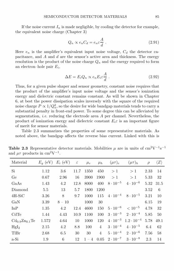
SEMICONDUCTOR DETECTOR MATERIALS 85
If the noise current In is made negligible, by cooling the detector for example,the equivalent noise charge (Chapter 3)
Qn ∝ enCd = enεA
d. (2.91)
Here en is the amplifier’s equivalent input noise voltage, Cd the detector ca-pacitance, and A and d are the sensor’s active area and thickness. The energyresolution is the product of the noise charge Qn and the energy required to forman electron–hole pair Ei,
∆E = EiQn ∝ enEiεA
d. (2.92)
Thus, for a given pulse shaper and sensor geometry, constant noise requires thatthe product of the amplifier’s input noise voltage and the sensor’s ionizationenergy and dielectric constant remains constant. As will be shown in Chapter6, at best the power dissipation scales inversely with the square of the requirednoise charge P ∝ 1/Q2
n, so the desire for wide bandgap materials tends to carry asubstantial penalty in front-end power. To some degree this can be alleviated bysegmentation, i.e. reducing the electrode area A per channel. Nevertheless, theproduct of ionization energy and dielectric constant Eiε is an important figureof merit for sensor materials.
Table 2.3 summarizes the properties of some representative materials. Asnoted above, the bandgap affects the reverse bias current. Linked with this is
Table 2.3 Representative detector materials. Mobilities µ are in units of cm2V−1s−1
and µτ products in cm2V−1.
Material Eg (eV) Ei (eV) ε µe µh (µτ)e (µτ)h ρ 〈Z〉
Si 1.12 3.6 11.7 1350 450 > 1 > 1 2.33 14
Ge 0.67 2.96 16 3900 1900 > 1 > 1 5.33 32
GaAs 1.43 4.2 12.8 8000 400 8 · 10−5 4 · 10−6 5.32 31.5
Diamond 5.5 13 5.7 1800 1200 3.52 6
4H-SiC 3.26 8 9.7 1000 115 4 · 10−4 8 · 10−5 3.21 10
GaN 3.39 8 – 10 1000 30 6.15 19
InP 1.35 4.2 12.4 4600 150 5 · 10−6 < 10−5 4.78 32
CdTe 1.44 4.43 10.9 1100 100 3 · 10−3 2 · 10−4 5.85 50
Cd0.9Zn0.1Te 1.572 4.64 10 1000 120 4 · 10−3 1.2 · 10−4 5.78 49.1
HgI2 2.15 4.2 8.8 100 4 3 · 10−4 4 · 10−5 6.4 62
TlBr 2.68 6.5 30 30 4 5 · 10−4 2 · 10−6 7.56 58
a-Si 1.9 6 12 1 – 4 0.05 2 · 10−7 3 · 10−8 2.3 14
86 SIGNAL FORMATION AND ACQUISITION
the ionization energy Ei, which sets the charge yield. The electronic noise is setby both the reverse bias current and the detector capacitance, which dependson the dielectric constant ε. The electron and hole mobilities µe and µh de-termine the collection time, whereas the mobility–lifetime products (µτ)e and(µτ)h indicate the maximum useful detector thickness. The density gives the en-ergy loss for minimum ionizing particles in high energy particle tracking and theatomic number is key in setting the absorption in x-ray and gamma detection.The data for diamond and amorphous silicon are for films deposited by chemicalvapor deposition, so the material is polycrystalline with properties strongly de-pendent on the growth conditions. Papers on diamond detectors quote a “chargecollection distance”, which specifies how far electrons and holes are separatedbefore recombination. A typical value for high-quality films is 200 µm at a fieldof 104 V/cm (Edwards 2004). The size of the microcrystals in diamond becomesvisible in precision measurements of the position resolution (Lari 2005).
For more details on materials for x-ray spectroscopy see Owens (2004). Moll(2003) and the RD50 website give information on radiation resistance. Com-pound semiconductors are of great interest in this context, as they allow thebandgap to be tuned by changing the composition (“bandgap engineering”). Forexample, in ZnTe the bandgap Eg = 2 eV and in CdTe it is 1.5 eV. Varying thecomposition x of Cd(1−x)ZnxTe changes the bandgap between the two extremes.Empirically it has been found that (Olega 1985)
Eg(x) = 1.510 + 0.606x + 0.139x2 eV . (2.93)
In compound semiconductors the hole mobility tends to be much smaller thanfor electrons. If the integration time of the electronics is tailored to the electroncollection time, the hole contribution may be negligible, so on the average onlyhalf the signal charge is available. For charged particles traversing the detectorthe signal will be the same, but for photons the induced electron signal willdepend on where the photon was absorbed. As shown in Section 2.5.3 the chargeinduced on small-pitch strip or pixel electrodes is preferentially due to the carriertype collected on the respective electrode. Furthermore, the charge induced onnon-collecting electrodes only integrates to zero after both carrier types havereached their respective electrodes. This can be exploited in coplanar strip arraysto mitigate the effect of incomplete hole collection. By ganging every other stripand subtracting the signals from the two sets the net electron signal is measured(Luke 1994, 1995, Amman and Luke 1999).
Work on alternative materials to complement Si and Ge has been pursued fordecades. Progress has been made and new materials have been applied in nicheareas. Clearly, many properties play together and developments in materialsgrowth technology can change the picture significantly.
2.8 Photodiodes
Photodiodes differ from charged particle and x-ray detectors in the very smallabsorption depth of visible light. As the photon energies are close to the bandgap,
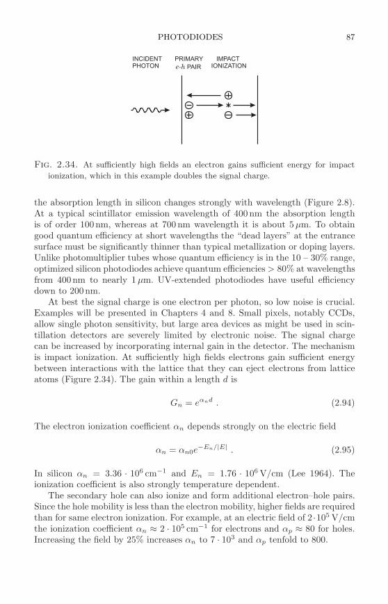
PHOTODIODES 87
PRIMARY
PAIRe-h
IMPACT
IONIZATION
INCIDENT
PHOTON
Fig. 2.34. At sufficiently high fields an electron gains sufficient energy for impact
ionization, which in this example doubles the signal charge.
the absorption length in silicon changes strongly with wavelength (Figure 2.8).At a typical scintillator emission wavelength of 400nm the absorption lengthis of order 100nm, whereas at 700nm wavelength it is about 5 µm. To obtaingood quantum efficiency at short wavelengths the “dead layers” at the entrancesurface must be significantly thinner than typical metallization or doping layers.Unlike photomultiplier tubes whose quantum efficiency is in the 10 – 30% range,optimized silicon photodiodes achieve quantum efficiencies > 80% at wavelengthsfrom 400nm to nearly 1 µm. UV-extended photodiodes have useful efficiencydown to 200nm.
At best the signal charge is one electron per photon, so low noise is crucial.Examples will be presented in Chapters 4 and 8. Small pixels, notably CCDs,allow single photon sensitivity, but large area devices as might be used in scin-tillation detectors are severely limited by electronic noise. The signal chargecan be increased by incorporating internal gain in the detector. The mechanismis impact ionization. At sufficiently high fields electrons gain sufficient energybetween interactions with the lattice that they can eject electrons from latticeatoms (Figure 2.34). The gain within a length d is
Gn = eαnd . (2.94)
The electron ionization coefficient αn depends strongly on the electric field
αn = αn0e−En/|E| . (2.95)
In silicon αn = 3.36 · 106 cm−1 and En = 1.76 · 106 V/cm (Lee 1964). Theionization coefficient is also strongly temperature dependent.
The secondary hole can also ionize and form additional electron–hole pairs.Since the hole mobility is less than the electron mobility, higher fields are requiredthan for same electron ionization. For example, at an electric field of 2 ·105 V/cmthe ionization coefficient αn ≈ 2 · 105 cm−1 for electrons and αp ≈ 80 for holes.Increasing the field by 25% increases αn to 7 · 103 and αp tenfold to 800.
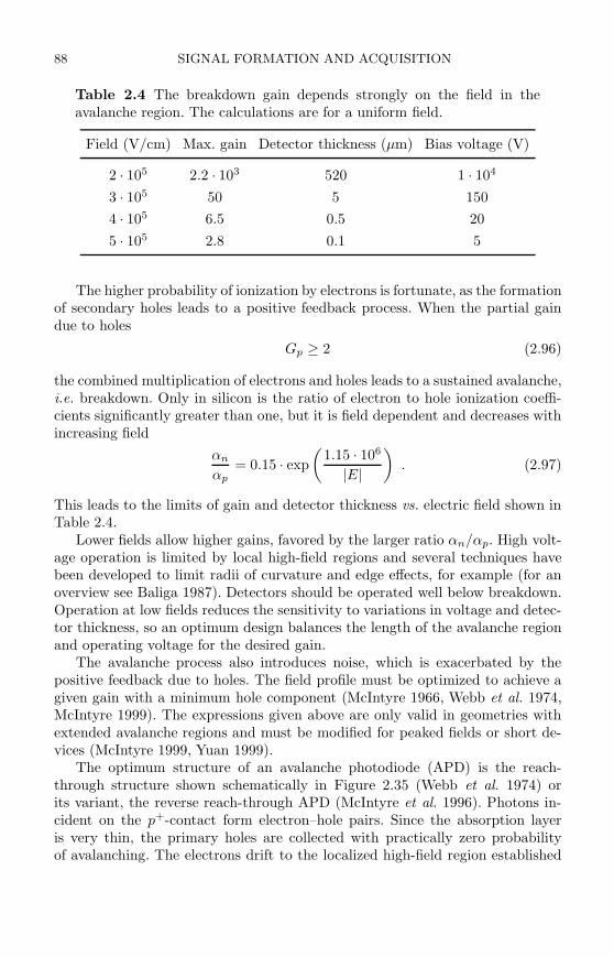
88 SIGNAL FORMATION AND ACQUISITION
Table 2.4 The breakdown gain depends strongly on the field in theavalanche region. The calculations are for a uniform field.
Field (V/cm) Max. gain Detector thickness (µm) Bias voltage (V)
2 · 105 2.2 · 103 520 1 · 104
3 · 105 50 5 150
4 · 105 6.5 0.5 20
5 · 105 2.8 0.1 5
The higher probability of ionization by electrons is fortunate, as the formationof secondary holes leads to a positive feedback process. When the partial gaindue to holes
Gp ≥ 2 (2.96)
the combined multiplication of electrons and holes leads to a sustained avalanche,i.e. breakdown. Only in silicon is the ratio of electron to hole ionization coeffi-cients significantly greater than one, but it is field dependent and decreases withincreasing field
αn
αp= 0.15 · exp
(
1.15 · 106
|E|
)
. (2.97)
This leads to the limits of gain and detector thickness vs. electric field shown inTable 2.4.
Lower fields allow higher gains, favored by the larger ratio αn/αp. High volt-age operation is limited by local high-field regions and several techniques havebeen developed to limit radii of curvature and edge effects, for example (for anoverview see Baliga 1987). Detectors should be operated well below breakdown.Operation at low fields reduces the sensitivity to variations in voltage and detec-tor thickness, so an optimum design balances the length of the avalanche regionand operating voltage for the desired gain.
The avalanche process also introduces noise, which is exacerbated by thepositive feedback due to holes. The field profile must be optimized to achieve agiven gain with a minimum hole component (McIntyre 1966, Webb et al. 1974,McIntyre 1999). The expressions given above are only valid in geometries withextended avalanche regions and must be modified for peaked fields or short de-vices (McIntyre 1999, Yuan 1999).
The optimum structure of an avalanche photodiode (APD) is the reach-through structure shown schematically in Figure 2.35 (Webb et al. 1974) orits variant, the reverse reach-through APD (McIntyre et al. 1996). Photons in-cident on the p+-contact form electron–hole pairs. Since the absorption layeris very thin, the primary holes are collected with practically zero probabilityof avalanching. The electrons drift to the localized high-field region established
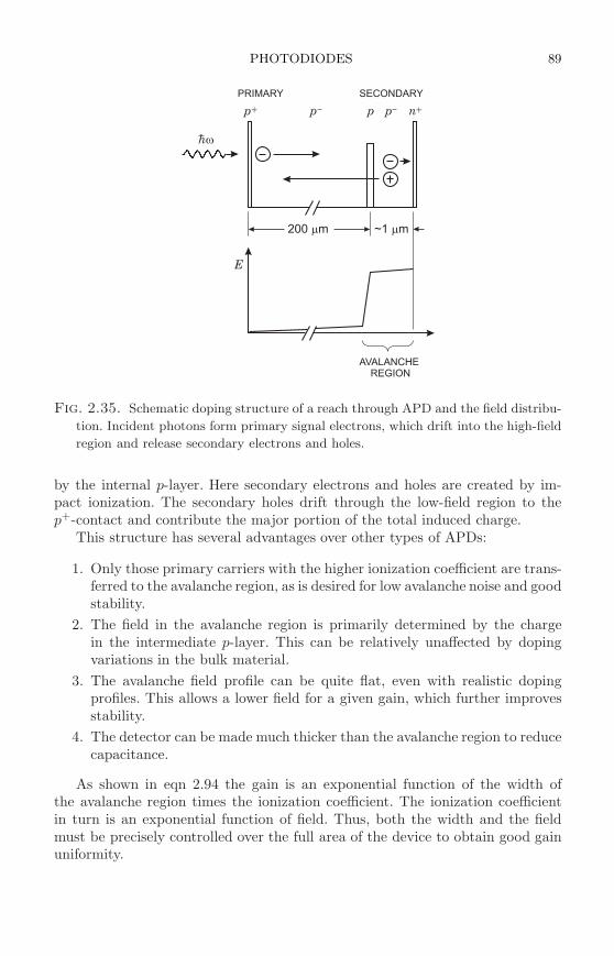
PHOTODIODES 89
200 m ~1 m
p pp p n+ +
E
AVALANCHE
REGION
PRIMARY SECONDARY
h
Fig. 2.35. Schematic doping structure of a reach through APD and the field distribu-
tion. Incident photons form primary signal electrons, which drift into the high-field
region and release secondary electrons and holes.
by the internal p-layer. Here secondary electrons and holes are created by im-pact ionization. The secondary holes drift through the low-field region to thep+-contact and contribute the major portion of the total induced charge.
This structure has several advantages over other types of APDs:
1. Only those primary carriers with the higher ionization coefficient are trans-ferred to the avalanche region, as is desired for low avalanche noise and goodstability.
2. The field in the avalanche region is primarily determined by the chargein the intermediate p-layer. This can be relatively unaffected by dopingvariations in the bulk material.
3. The avalanche field profile can be quite flat, even with realistic dopingprofiles. This allows a lower field for a given gain, which further improvesstability.
4. The detector can be made much thicker than the avalanche region to reducecapacitance.
As shown in eqn 2.94 the gain is an exponential function of the width ofthe avalanche region times the ionization coefficient. The ionization coefficientin turn is an exponential function of field. Thus, both the width and the fieldmust be precisely controlled over the full area of the device to obtain good gainuniformity.
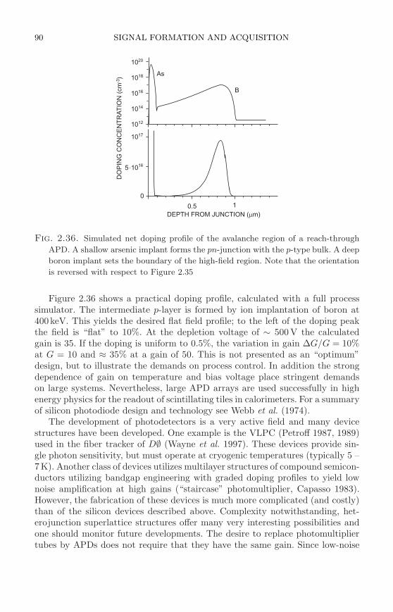
90 SIGNAL FORMATION AND ACQUISITION
10
10
10
10
10
10
17
16
14
12
16
18
20
0
105
0.5 1
DEPTH FROM JUNCTION ( m)
DO
PIN
GC
ON
CE
NT
RA
TIO
N(c
m)
-3
As
B
Fig. 2.36. Simulated net doping profile of the avalanche region of a reach-through
APD. A shallow arsenic implant forms the pn-junction with the p-type bulk. A deep
boron implant sets the boundary of the high-field region. Note that the orientation
is reversed with respect to Figure 2.35
Figure 2.36 shows a practical doping profile, calculated with a full processsimulator. The intermediate p-layer is formed by ion implantation of boron at400keV. This yields the desired flat field profile; to the left of the doping peakthe field is “flat” to 10%. At the depletion voltage of ∼ 500 V the calculatedgain is 35. If the doping is uniform to 0.5%, the variation in gain ∆G/G = 10%at G = 10 and ≈ 35% at a gain of 50. This is not presented as an “optimum”design, but to illustrate the demands on process control. In addition the strongdependence of gain on temperature and bias voltage place stringent demandson large systems. Nevertheless, large APD arrays are used successfully in highenergy physics for the readout of scintillating tiles in calorimeters. For a summaryof silicon photodiode design and technology see Webb et al. (1974).
The development of photodetectors is a very active field and many devicestructures have been developed. One example is the VLPC (Petroff 1987, 1989)used in the fiber tracker of D∅ (Wayne et al. 1997). These devices provide sin-gle photon sensitivity, but must operate at cryogenic temperatures (typically 5 –7K). Another class of devices utilizes multilayer structures of compound semicon-ductors utilizing bandgap engineering with graded doping profiles to yield lownoise amplification at high gains (“staircase” photomultiplier, Capasso 1983).However, the fabrication of these devices is much more complicated (and costly)than of the silicon devices described above. Complexity notwithstanding, het-erojunction superlattice structures offer many very interesting possibilities andone should monitor future developments. The desire to replace photomultipliertubes by APDs does not require that they have the same gain. Since low-noise
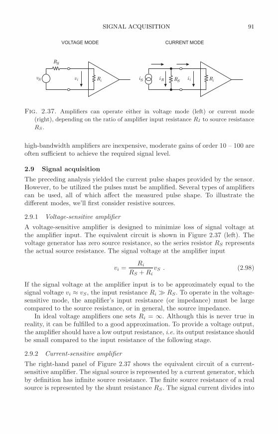
SIGNAL ACQUISITION 91
R Ri iiS iS iR
VOLTAGE MODE CURRENT MODE
R
Rv v
S
iS i
Fig. 2.37. Amplifiers can operate either in voltage mode (left) or current mode
(right), depending on the ratio of amplifier input resistance RI to source resistance
RS .
high-bandwidth amplifiers are inexpensive, moderate gains of order 10 – 100 areoften sufficient to achieve the required signal level.
2.9 Signal acquisition
The preceding analysis yielded the current pulse shapes provided by the sensor.However, to be utilized the pulses must be amplified. Several types of amplifierscan be used, all of which affect the measured pulse shape. To illustrate thedifferent modes, we’ll first consider resistive sources.
2.9.1 Voltage-sensitive amplifier
A voltage-sensitive amplifier is designed to minimize loss of signal voltage atthe amplifier input. The equivalent circuit is shown in Figure 2.37 (left). Thevoltage generator has zero source resistance, so the series resistor RS representsthe actual source resistance. The signal voltage at the amplifier input
vi =Ri
RS + RivS . (2.98)
If the signal voltage at the amplifier input is to be approximately equal to thesignal voltage vi ≈ vS , the input resistance Ri ≫ RS . To operate in the voltage-sensitive mode, the amplifier’s input resistance (or impedance) must be largecompared to the source resistance, or in general, the source impedance.
In ideal voltage amplifiers one sets Ri = ∞. Although this is never true inreality, it can be fulfilled to a good approximation. To provide a voltage output,the amplifier should have a low output resistance, i.e. its output resistance shouldbe small compared to the input resistance of the following stage.
2.9.2 Current-sensitive amplifier
The right-hand panel of Figure 2.37 shows the equivalent circuit of a current-sensitive amplifier. The signal source is represented by a current generator, whichby definition has infinite source resistance. The finite source resistance of a realsource is represented by the shunt resistance RS . The signal current divides into
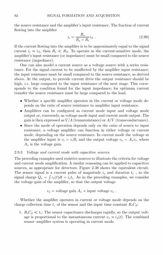
92 SIGNAL FORMATION AND ACQUISITION
the source resistance and the amplifier’s input resistance. The fraction of currentflowing into the amplifier
ii =Rs
Rs + RiiS . (2.99)
If the current flowing into the amplifier is to be approximately equal to the signalcurrent ii ≈ iS , then Ri ≪ RS . To operate in the current-sensitive mode, theamplifier’s input resistance (or impedance) must be small compared to the sourceresistance (impedance).
One can also model a current source as a voltage source with a series resis-tance. For the signal current to be unaffected by the amplifier input resistance,the input resistance must be small compared to the source resistance, as derivedabove. At the output, to provide current drive the output resistance should behigh, i.e. large compared to the input resistance of the next stage. This corre-sponds to the condition found for the input impedance; for optimum currenttransfer the source resistance must be large compared to the load.
• Whether a specific amplifier operates in the current or voltage mode de-pends on the ratio of source resistance to amplifier input resistance.
• Amplifiers can be configured as current mode input and voltage modeoutput or, conversely, as voltage mode input and current mode output. Thegain is then expressed as V/A (transresistance) or A/V (transconductance).
• Since the mode of operation depends only on the ratio of source to inputresistance, a voltage amplifier can function in either voltage or currentmode, depending on the source resistance. In current mode the voltage atthe amplifier input is vi = iiRi and the output voltage vo = Avvi, whereAv is the voltage gain.
2.9.3 Voltage and current mode with capacitive sources
The preceding examples used resistive sources to illustrate the criteria for voltageand current mode amplification. A similar reasoning can be applied to capacitivesources, as appropriate for detectors. Figure 2.38 shows the equivalent circuit.The sensor signal is a current pulse of magnitude is and duration tc , so thesignal charge Qs =
∫
is(t)dt = istc. As in the preceding examples, we considerthe voltage gain of the amplifier, so that the output voltage
vo = voltage gain Av × input voltage vs .
Whether the amplifier operates in current or voltage mode depends on thecharge collection time tc of the sensor and the input time constant RiCd:
1. RiCd ≪ tc: The sensor capacitance discharges rapidly, so the output volt-age is proportional to the instantaneous current vo ∝ is(t). The combinedsensor–amplifier system is operating in current mode.
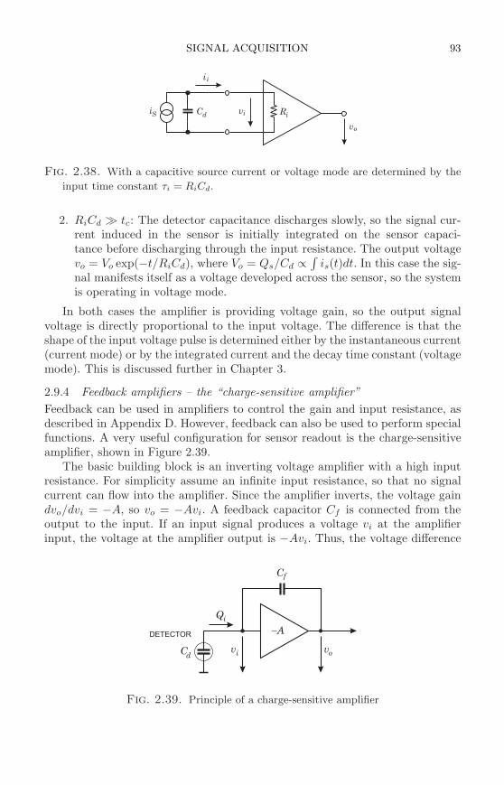
SIGNAL ACQUISITION 93
C Ri v
v
i
d iS i
o
i
Fig. 2.38. With a capacitive source current or voltage mode are determined by the
input time constant τi = RiCd.
2. RiCd ≫ tc: The detector capacitance discharges slowly, so the signal cur-rent induced in the sensor is initially integrated on the sensor capaci-tance before discharging through the input resistance. The output voltagevo = Vo exp(−t/RiCd), where Vo = Qs/Cd ∝
∫
is(t)dt. In this case the sig-nal manifests itself as a voltage developed across the sensor, so the systemis operating in voltage mode.
In both cases the amplifier is providing voltage gain, so the output signalvoltage is directly proportional to the input voltage. The difference is that theshape of the input voltage pulse is determined either by the instantaneous current(current mode) or by the integrated current and the decay time constant (voltagemode). This is discussed further in Chapter 3.
2.9.4 Feedback amplifiers – the “charge-sensitive amplifier”
Feedback can be used in amplifiers to control the gain and input resistance, asdescribed in Appendix D. However, feedback can also be used to perform specialfunctions. A very useful configuration for sensor readout is the charge-sensitiveamplifier, shown in Figure 2.39.
The basic building block is an inverting voltage amplifier with a high inputresistance. For simplicity assume an infinite input resistance, so that no signalcurrent can flow into the amplifier. Since the amplifier inverts, the voltage gaindvo/dvi = −A, so vo = −Avi. A feedback capacitor Cf is connected from theoutput to the input. If an input signal produces a voltage vi at the amplifierinput, the voltage at the amplifier output is −Avi. Thus, the voltage difference
v
Q
C
C vi
i
f
d o
ADETECTOR
Fig. 2.39. Principle of a charge-sensitive amplifier
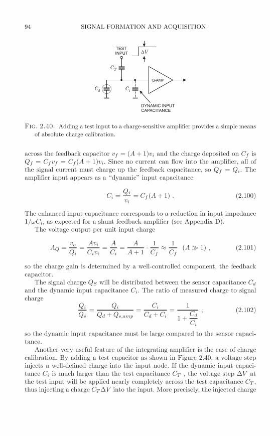
94 SIGNAL FORMATION AND ACQUISITION
C
C
Ci
T
d
Q-AMP
VTEST
INPUT
DYNAMIC INPUT
CAPACITANCE
Fig. 2.40. Adding a test input to a charge-sensitive amplifier provides a simple means
of absolute charge calibration.
across the feedback capacitor vf = (A + 1)vi and the charge deposited on Cf isQf = Cfvf = Cf (A + 1)vi. Since no current can flow into the amplifier, all ofthe signal current must charge up the feedback capacitance, so Qf = Qi. Theamplifier input appears as a “dynamic” input capacitance
Ci =Qi
vi= Cf (A + 1) . (2.100)
The enhanced input capacitance corresponds to a reduction in input impedance1/ωCi, as expected for a shunt feedback amplifier (see Appendix D).
The voltage output per unit input charge
AQ =vo
Qi=
Avi
Civi=
A
Ci=
A
A + 1· 1
Cf≈ 1
Cf(A ≫ 1) , (2.101)
so the charge gain is determined by a well-controlled component, the feedbackcapacitor.
The signal charge QS will be distributed between the sensor capacitance Cd
and the dynamic input capacitance Ci. The ratio of measured charge to signalcharge
Qi
Qs=
Qi
Qd + Qs,amp=
Ci
Cd + Ci=
1
1 +Cd
Ci
, (2.102)
so the dynamic input capacitance must be large compared to the sensor capaci-tance.
Another very useful feature of the integrating amplifier is the ease of chargecalibration. By adding a test capacitor as shown in Figure 2.40, a voltage stepinjects a well-defined charge into the input node. If the dynamic input capaci-tance Ci is much larger than the test capacitance CT , the voltage step ∆V atthe test input will be applied nearly completely across the test capacitance CT ,thus injecting a charge CT ∆V into the input. More precisely, the injected charge
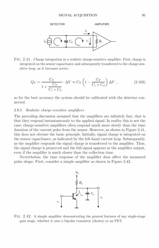
SIGNAL ACQUISITION 95
DETECTOR
C R
AMPLIFIER
i v
i
s id
i
i
Fig. 2.41. Charge integration in a realistic charge-sensitive amplifier. First, charge is
integrated on the sensor capacitance and subsequently transferred to the charge-sen-
sitive loop, as it becomes active.
QT =CT
1 +CT
Ci + Cd
· ∆V ≈ CT
(
1 − CT
Ci + Cd
)
∆V , (2.103)
so for the best accuracy the system should be calibrated with the detector con-nected.
2.9.5 Realistic charge-sensitive amplifiers
The preceding discussion assumed that the amplifiers are infinitely fast, that isthat they respond instantaneously to the applied signal. In reality this is not thecase; charge-sensitive amplifiers often respond much more slowly than the timeduration of the current pulse from the sensor. However, as shown in Figure 2.41,this does not obviate the basic principle. Initially, signal charge is integrated onthe sensor capacitance, as indicated by the left-hand current loop. Subsequently,as the amplifier responds the signal charge is transferred to the amplifier. Thus,the signal charge is preserved and the full signal appears at the amplifier output,even if the amplifier is much slower than the collection time.
Nevertheless, the time response of the amplifier does affect the measuredpulse shape. First, consider a simple amplifier as shown in Figure 2.42.
V+
v
i C
R
v
i
oo
L
o
Fig. 2.42. A simple amplifier demonstrating the general features of any single-stage
gain stage, whether it uses a bipolar transistor (shown) or an FET.
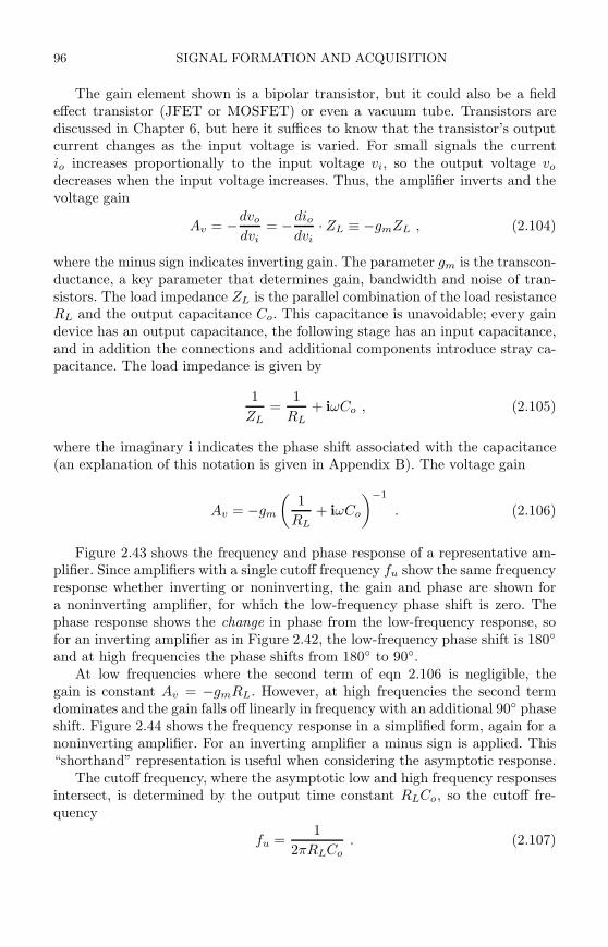
96 SIGNAL FORMATION AND ACQUISITION
The gain element shown is a bipolar transistor, but it could also be a fieldeffect transistor (JFET or MOSFET) or even a vacuum tube. Transistors arediscussed in Chapter 6, but here it suffices to know that the transistor’s outputcurrent changes as the input voltage is varied. For small signals the currentio increases proportionally to the input voltage vi, so the output voltage vo
decreases when the input voltage increases. Thus, the amplifier inverts and thevoltage gain
Av = −dvo
dvi= −dio
dvi· ZL ≡ −gmZL , (2.104)
where the minus sign indicates inverting gain. The parameter gm is the transcon-ductance, a key parameter that determines gain, bandwidth and noise of tran-sistors. The load impedance ZL is the parallel combination of the load resistanceRL and the output capacitance Co. This capacitance is unavoidable; every gaindevice has an output capacitance, the following stage has an input capacitance,and in addition the connections and additional components introduce stray ca-pacitance. The load impedance is given by
1
ZL=
1
RL+ iωCo , (2.105)
where the imaginary i indicates the phase shift associated with the capacitance(an explanation of this notation is given in Appendix B). The voltage gain
Av = −gm
(
1
RL+ iωCo
)−1
. (2.106)
Figure 2.43 shows the frequency and phase response of a representative am-plifier. Since amplifiers with a single cutoff frequency fu show the same frequencyresponse whether inverting or noninverting, the gain and phase are shown fora noninverting amplifier, for which the low-frequency phase shift is zero. Thephase response shows the change in phase from the low-frequency response, sofor an inverting amplifier as in Figure 2.42, the low-frequency phase shift is 180
and at high frequencies the phase shifts from 180 to 90.At low frequencies where the second term of eqn 2.106 is negligible, the
gain is constant Av = −gmRL. However, at high frequencies the second termdominates and the gain falls off linearly in frequency with an additional 90 phaseshift. Figure 2.44 shows the frequency response in a simplified form, again for anoninverting amplifier. For an inverting amplifier a minus sign is applied. This“shorthand” representation is useful when considering the asymptotic response.
The cutoff frequency, where the asymptotic low and high frequency responsesintersect, is determined by the output time constant RLCo, so the cutoff fre-quency
fu =1
2πRLCo. (2.107)
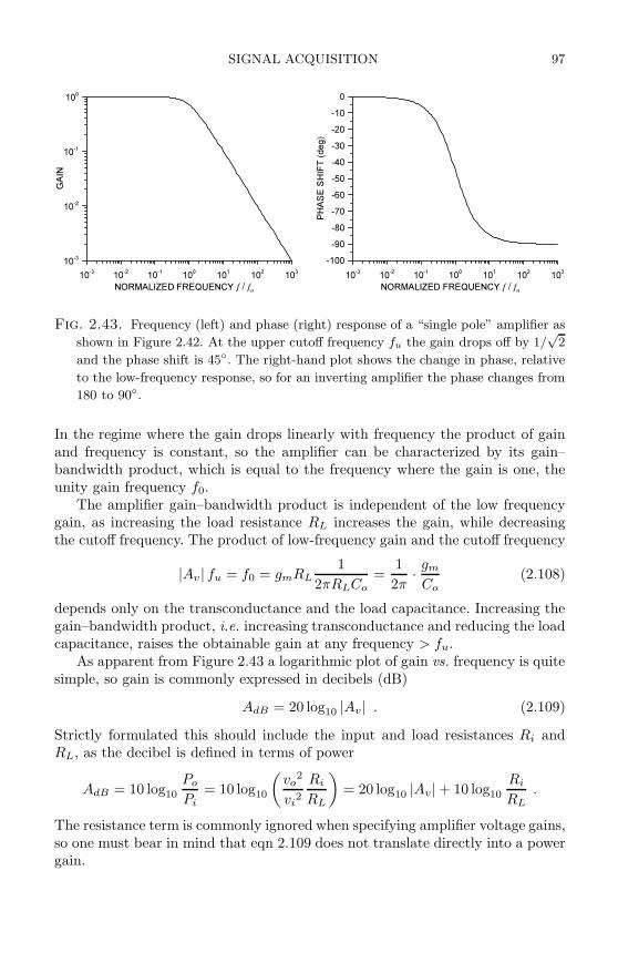
SIGNAL ACQUISITION 97
10-3
10-2
10-1
100
101
102
103
NORMALIZED FREQUENCY f / fu
10-3
10-2
10-1
100
GAIN
10-3
10-2
10-1
100
101
102
103
NORMALIZED FREQUENCY f / fu
-100
-90
-80
-70
-60
-50
-40
-30
-20
-10
0
PHASESHIFT(deg)
Fig. 2.43. Frequency (left) and phase (right) response of a “single pole” amplifier as
shown in Figure 2.42. At the upper cutoff frequency fu the gain drops off by 1/√
2
and the phase shift is 45. The right-hand plot shows the change in phase, relative
to the low-frequency response, so for an inverting amplifier the phase changes from
180 to 90.
In the regime where the gain drops linearly with frequency the product of gainand frequency is constant, so the amplifier can be characterized by its gain–bandwidth product, which is equal to the frequency where the gain is one, theunity gain frequency f0.
The amplifier gain–bandwidth product is independent of the low frequencygain, as increasing the load resistance RL increases the gain, while decreasingthe cutoff frequency. The product of low-frequency gain and the cutoff frequency
|Av | fu = f0 = gmRL1
2πRLCo=
1
2π· gm
Co(2.108)
depends only on the transconductance and the load capacitance. Increasing thegain–bandwidth product, i.e. increasing transconductance and reducing the loadcapacitance, raises the obtainable gain at any frequency > fu.
As apparent from Figure 2.43 a logarithmic plot of gain vs. frequency is quitesimple, so gain is commonly expressed in decibels (dB)
AdB = 20 log10 |Av | . (2.109)
Strictly formulated this should include the input and load resistances Ri andRL, as the decibel is defined in terms of power
AdB = 10 log10
Po
Pi= 10 log10
(
vo2
vi2
Ri
RL
)
= 20 log10 |Av| + 10 log10
Ri
RL.
The resistance term is commonly ignored when specifying amplifier voltage gains,so one must bear in mind that eqn 2.109 does not translate directly into a powergain.
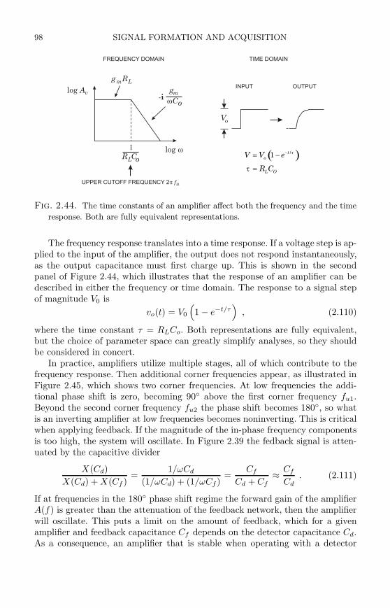
98 SIGNAL FORMATION AND ACQUISITION
log A
log
v
g R
R
g
1
m L
L
m-i
C
C
o
o
UPPER CUTOFF FREQUENCY 2 fu
Vo
FREQUENCY DOMAIN TIME DOMAIN
INPUT OUTPUT
/1 t
o
L O
V V e
R C
Fig. 2.44. The time constants of an amplifier affect both the frequency and the time
response. Both are fully equivalent representations.
The frequency response translates into a time response. If a voltage step is ap-plied to the input of the amplifier, the output does not respond instantaneously,as the output capacitance must first charge up. This is shown in the secondpanel of Figure 2.44, which illustrates that the response of an amplifier can bedescribed in either the frequency or time domain. The response to a signal stepof magnitude V0 is
vo(t) = V0
(
1 − e−t/τ)
, (2.110)
where the time constant τ = RLCo. Both representations are fully equivalent,but the choice of parameter space can greatly simplify analyses, so they shouldbe considered in concert.
In practice, amplifiers utilize multiple stages, all of which contribute to thefrequency response. Then additional corner frequencies appear, as illustrated inFigure 2.45, which shows two corner frequencies. At low frequencies the addi-tional phase shift is zero, becoming 90 above the first corner frequency fu1.Beyond the second corner frequency fu2 the phase shift becomes 180, so whatis an inverting amplifier at low frequencies becomes noninverting. This is criticalwhen applying feedback. If the magnitude of the in-phase frequency componentsis too high, the system will oscillate. In Figure 2.39 the fedback signal is atten-uated by the capacitive divider
X(Cd)
X(Cd) + X(Cf )=
1/ωCd
(1/ωCd) + (1/ωCf )=
Cf
Cd + Cf≈ Cf
Cd. (2.111)
If at frequencies in the 180 phase shift regime the forward gain of the amplifierA(f) is greater than the attenuation of the feedback network, then the amplifierwill oscillate. This puts a limit on the amount of feedback, which for a givenamplifier and feedback capacitance Cf depends on the detector capacitance Cd.As a consequence, an amplifier that is stable when operating with a detector
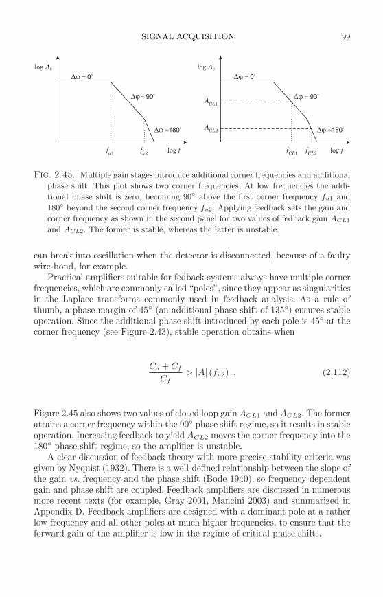
SIGNAL ACQUISITION 99
log A log Av v
u1 CL1
CL2
CL1
u2 CL2
0o 0
o
90o 90
o
180o 180
o
f f
A
A
f flog f log f
Fig. 2.45. Multiple gain stages introduce additional corner frequencies and additional
phase shift. This plot shows two corner frequencies. At low frequencies the addi-
tional phase shift is zero, becoming 90 above the first corner frequency fu1 and
180 beyond the second corner frequency fu2. Applying feedback sets the gain and
corner frequency as shown in the second panel for two values of fedback gain ACL1
and ACL2. The former is stable, whereas the latter is unstable.
can break into oscillation when the detector is disconnected, because of a faultywire-bond, for example.
Practical amplifiers suitable for fedback systems always have multiple cornerfrequencies, which are commonly called “poles”, since they appear as singularitiesin the Laplace transforms commonly used in feedback analysis. As a rule ofthumb, a phase margin of 45 (an additional phase shift of 135) ensures stableoperation. Since the additional phase shift introduced by each pole is 45 at thecorner frequency (see Figure 2.43), stable operation obtains when
Cd + Cf
Cf> |A| (fu2) . (2.112)
Figure 2.45 also shows two values of closed loop gain ACL1 and ACL2. The formerattains a corner frequency within the 90 phase shift regime, so it results in stableoperation. Increasing feedback to yield ACL2 moves the corner frequency into the180 phase shift regime, so the amplifier is unstable.
A clear discussion of feedback theory with more precise stability criteria wasgiven by Nyquist (1932). There is a well-defined relationship between the slope ofthe gain vs. frequency and the phase shift (Bode 1940), so frequency-dependentgain and phase shift are coupled. Feedback amplifiers are discussed in numerousmore recent texts (for example, Gray 2001, Mancini 2003) and summarized inAppendix D. Feedback amplifiers are designed with a dominant pole at a ratherlow frequency and all other poles at much higher frequencies, to ensure that theforward gain of the amplifier is low in the regime of critical phase shifts.
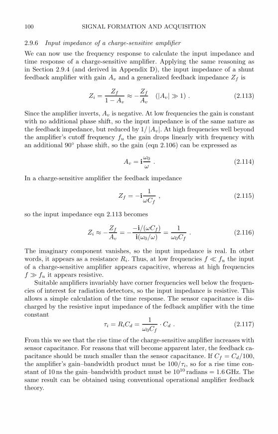
100 SIGNAL FORMATION AND ACQUISITION
2.9.6 Input impedance of a charge-sensitive amplifier
We can now use the frequency response to calculate the input impedance andtime response of a charge-sensitive amplifier. Applying the same reasoning asin Section 2.9.4 (and derived in Appendix D), the input impedance of a shuntfeedback amplifier with gain Av and a generalized feedback impedance Zf is
Zi =Zf
1 − Av≈ −Zf
Av(|Av | ≫ 1) . (2.113)
Since the amplifier inverts, Av is negative. At low frequencies the gain is constantwith no additional phase shift, so the input impedance is of the same nature asthe feedback impedance, but reduced by 1/ |Av|. At high frequencies well beyondthe amplifier’s cutoff frequency fu the gain drops linearly with frequency withan additional 90 phase shift, so the gain (eqn 2.106) can be expressed as
Av = iω0
ω. (2.114)
In a charge-sensitive amplifier the feedback impedance
Zf = −i1
ωCf, (2.115)
so the input impedance eqn 2.113 becomes
Zi ≈ −Zf
Av= −−i/(ωCf )
i(ω0/ω)=
1
ω0Cf. (2.116)
The imaginary component vanishes, so the input impedance is real. In otherwords, it appears as a resistance Ri. Thus, at low frequencies f ≪ fu the inputof a charge-sensitive amplifier appears capacitive, whereas at high frequenciesf ≫ fu it appears resistive.
Suitable amplifiers invariably have corner frequencies well below the frequen-cies of interest for radiation detectors, so the input impedance is resistive. Thisallows a simple calculation of the time response. The sensor capacitance is dis-charged by the resistive input impedance of the fedback amplifier with the timeconstant
τi = RiCd =1
ω0Cf· Cd . (2.117)
From this we see that the rise time of the charge-sensitive amplifier increases withsensor capacitance. For reasons that will become apparent later, the feedback ca-pacitance should be much smaller than the sensor capacitance. If Cf = Cd/100,the amplifier’s gain–bandwidth product must be 100/τi, so for a rise time con-stant of 10 ns the gain–bandwidth product must be 1010 radians = 1.6GHz. Thesame result can be obtained using conventional operational amplifier feedbacktheory.
SIGNAL ACQUISITION 101
C C C C
C C C C C
ss ss ss ss
b b b b b
STRIP
DETECTOR
Fig. 2.46. To preserve the position resolution of strip detectors the readout amplifiers
must have a low input impedance to prevent spreading of signal charge to the
neighboring electrodes.
In acquiring the signal the ohmic input impedance at high frequencies andthe dynamic input capacitance at low frequencies play complementary roles. Ina simple approximation the charge transferred to the amplifier
Q(t) ≈ Qs
1 +Cd
Ci
(
1 − e−t/τi
)
. (2.118)
The input time constant τi = RiCd determines how quickly charge is trans-ferred from the detector and the dynamic input capacitance Ci determines whatfraction of the signal charge Qs can be acquired.
The mechanism of reducing the input impedance through shunt feedbackleads to the concept of the “virtual ground”. If the gain is infinite, the inputimpedance is zero. Although very high gains (of order 105 – 106) are achiev-able in the kHz range, at the frequencies relevant for detector signals the gainis much smaller. The input impedance of typical charge-sensitive amplifiers instrip detector systems is of order kΩ. Fast amplifiers designed to optimize powerdissipation achieve input impedances of 100 – 500Ω (Kipnis 1994). None of thesequalify as a “virtual ground”, so this concept should be applied with caution.
Apart from determining the signal rise time, the input impedance is criti-cal in position-sensitive detectors. Figure 2.46 illustrates a silicon-strip sensorread out by a bank of amplifiers. Each strip electrode has a capacitance Cb tothe backplane and a fringing capacitance Css to the neighboring strips. If theamplifier has an infinite input impedance, charge induced on one strip will ca-pacitively couple to the neighbors and the signal will be distributed over manystrips (determined by Css/Cb ). If, on the other hand, the input impedance of theamplifier is low compared to interstrip impedance, practically all of the chargewill flow into the amplifier and the neighbors will show only a small signal. Therelevant frequencies are set by the peaking time TP of the pulse shaper.
102 SIGNAL FORMATION AND ACQUISITION
For strip pitches that are much smaller than the bulk thickness the capac-itance is dominated by the fringing capacitance to the neighboring strips Css.Typically, the fringing capacitance is 1 – 2pF/cm for strip pitches of 25 – 100µmon Si. The backplane capacitance Cb is typically 20% of the strip-to-strip capac-itance. If the real part of the amplifier’s input impedance is Ri, cross-couplingwill be negligible at times greater than 2 to 3 times RiCss and if Ci ≫ Css.
References
Alkhazov, G.D. et al. (1967). Ionization fluctuations and resolution of ionizationchambers and semiconductor detectors. Nucl. Instr. and Meth. 48 (1967) 1–12
Amman, M. and Luke, P.N. (1999). Optimization criteria for coplanar-grid de-tectors. IEEE Trans. Nucl. Sci. NS-46/3 205–212
Avset, B.S. et al. (1990). A new microstrip detector with double-sided readout.IEEE Trans. Nucl. Sci. 37/3 (1990) 1153–1161
Baliga, B. Jayant (1987). Modern Power Devices. Chapter 3. Wiley, New York.ISBN 0-471-81986-7, TK7881.15.B35
Beadle, W.C. , Tsai, J.C.C., and Plummer, R.D. (1984). Quick Reference Man-ual for Silicon Integrated Circuit Technology. Wiley-Interscience, New York,ISBN 0-471-81588-8, TK7874.Q38 1984
Bode, H.W. (1940). Relations between attenuation and phase in feedback am-plifier design. Bell System Tech. Journal 19 (1940) 421–454
Cavalleri, G. et al. (1971). Extension of Ramo’s theorem to induced charge insemiconductor detectors. Nucl. Instr. and Meth. 92 (1971) 137–140
Chabaud, V. et al. (1996). The DELPHI silicon strip microvertex detector withdouble sided readout. Nucl. Instr. and Meth. A368 (1996) 314–332
Conradi, J. (1972). The distribution of gains in uniformly multiplying ava-lanche photodiodes: experimental. IEEE Trans. Electron Dev. ED-19/6 (1972)713–718
Edwards, A.J. et al. (2004). Radiation monitoring with diamond sensors inBaBar. IEEE Trans. Nucl. Sci. NS51/4 (2004) 1808–1811
Fano, U. (1947). Ionization yield of radiations. II. The fluctuations of the num-ber of ions. Phys. Rev. 72 (1947) 26–29
Gray, Paul R. et al. (2001). Analysis and Design of Analog Integrated Circuits.(4th edn). Wiley, New York, ISBN 0-471-32168-0
Haller, E.E., Hansen, W.L., and Goulding, F.S. (1981). Physics of ultra-puregermanium. Advances in Physics 30(1) (1981) 93–138
Hecht, K. (1932). Zum Mechanismus des lichtelektrischen Primarstroms in iso-lierenden Kristallen. Z. Physik 77 (1932) 235–245
Kittel, C. (1996). Introduction to Solid State Physics. Wiley, New York, ISBN0-471-11181-3, QC176.K5 1996.
Klein, C.A. (1968). Bandgap dependence and related features of radiation ion-ization energies in semiconductors. J. Applied Physics 39 (1968) 2029–2038
REFERENCES 103
Lari, T. et al. (2005). Characterization and modeling of non-uniform charge col-lection in CVD diamond pixel detectors. Nucl. Instr. and Meth. A537 (2005)581–593
Lee, C.A. et al. (1964) Ionization rates of holes and electrons in silicon. Phys.Rev. 134/3A (1964) A761–A773
Luke, P.N. (1994). Single-polarity charge sensing in ionization detectors usingcoplanar electrodes. Appl. Phys. Lett. 65 (1994) 2884–2886
Luke, P.N. (1995). Unipolar charge sensing with coplanar electrodes – Appli-cation to Semiconductor Detectors. IEEE Trans. Nucl. Sci. NS-42/4 (1995)207–213
Mancini, R. (2003). Op Amps for Everyone (2nd edn), Newnes, Amsterdam,ISBN 0-750-67701-5
McIntyre, R.J. (1966). Multiplication noise in uniform avalanche diodes. IEEETrans. Electron Dev. ED-13/1 (1966) 164–168
McIntyre, R.J. (1966). The distribution of gains in uniformly multiplying ava-lanche photodiodes: theory. IEEE Trans. Electron Dev. ED-19/6 (1972) 703–713
McIntyre, R.J. et al. (1996). A short-wavelength selective reach-through ava-lanche photodiode. IEEE Trans. Nucl. Sci. NS-43/3 (1996) 1341–1346
McIntyre, R.J. (1999). A new look at impact ionization – Part I: A theoryof gain, noise, breakdown probability, and frequency response. IEEE Trans.Electron Dev. ED-46/8 (1999) 1623–1631
Nyquist, H. (1932). Regeneration theory. Bell System Tech. Journal 11 (1932)126–147
Owens, A. et al.(1999). Synchrotron characterization of deep depletion epitaxialGaAs detectors. J. Appl. Phys. 86 (1999) 4341–4347
Owens, A. and Peacock, A. (2004). Compound semiconductor radiation detec-tors. Nucl. Instr. and Meth. A531 (2004) 18–37
Petroff, M.D. et al. (1987). Detection of individual 0.4 – 28µm wavelengthphotons via impurity-impact ionization in a solid-state photomultiplier. Appl.Phys. Lett. 51 (1987) 406–408
Petroff, M.D. and Stapelbroek, M.G. (1989). Photon-counting solid-state pho-tomultiplier. Nucl. Instr. and Meth. NS-36/1 (1989) 158–162
Queisser, H.J. and Haller, E.E. (1998). Defects in semiconductors: some fatal,some vital. Science 281 (1998) 945–950
Radeka, V. (1988). Low noise techniques in detectors. Ann. Rev. Nucl. Part.Sci. 38(1988) 217–277
Ramo, S. (1939). Currents induced by electron motion. Proc. IRE 27 (1939)584–585
Richter, R.H. et al. (1996). Strip detector design for ATLAS and HERA-Busing two-dimensional device simulation. Nucl. Instr. and Meth. A377 (1996)412–421
104 SIGNAL FORMATION AND ACQUISITION
Scholze, F. et al. (2000). Determination of the electron–hole pair creation energyfor semiconductors from the spectral responsivity of photodiodes. Nucl. Instr.and Meth. A439 (2000) 208–215
Shockley, W. (1938). Currents to conductors induced by a moving point charge.J. Appl. Phys. 9 (1938) 635–636
Shockley, W. (1950). Electrons and Holes in Semiconductors. van Nostrand,Princeton
Sze, S.M. (1981). Physics of Semiconductor Devices (2nd edn). Wiley, NewYork. ISBN 0-471-05661-8, TK7871.85.S988
Sze, S.M. (2001). Semiconductor Devices – Physics and Technology (2nd edn).Wiley, New York. ISBN 0-471-33372-7, TK7871.85.S9883
van Roosbroeck, W. (1963). Theory of the yield and Fano factor of electron–hole pairs generated in semiconductors by high-energy particles. Phys. Rev.139 (1963) A1702
Wayne, M.R. et al. (1997). Visible light photon counters and the D∅ scintillatingfiber tracker. Nucl. Instr. and Meth. A387 (1997) 278–281
Webb, P.P., McIntyre, R.J. and Conradi, J. (1972). Properties of avalanchephotodiodes. RCA Review 25 (1974) 234–278
Yuan, P. et al. (1999). A new Look at impact ionization – Part II: Gain andnoise in short avalanche photodiodes. IEEE Trans. Electron Dev. ED-46/8(1999) 1623–1631

CONTENTS
1 Detector systems overview 11.1 Sensor 21.2 Preamplifier 31.3 Pulse shaper 31.4 Digitizer 51.5 Electro–mechanical integration 61.6 Sensor structures I 8
1.6.1 Basic sensor 81.6.2 Position sensing 91.6.3 Pixel devices 11
1.7 Sensor physics 121.7.1 Signal charge 121.7.2 Sensor volume 131.7.3 Charge collection 161.7.4 Energy resolution 191.7.5 Position resolution 19
1.8 Sensor structures II – monolithic pixel devices 241.8.1 Charge coupled devices 241.8.2 Silicon drift chambers 251.8.3 Monolithic active pixel sensors 26
1.9 Electronics 291.10 Detection limits and resolution 29
1.10.1 Electronic noise 311.10.2 Amplitude measurements 331.10.3 Timing measurements 35
1.11 Subsystems 361.11.1 Circuit integration and bussing 361.11.2 Detector modules, services, and supports 381.11.3 Data acquisition 40
1.12 Further reading 40References 40
2 Signal formation and acquisition 432.1 The signal 432.2 Detector sensitivity 48
2.2.1 Low energy quanta (E ≈ Eg) 482.2.2 High energy quanta (E ≫ Eg) 512.2.3 Fluctuations in signal charge – the Fano factor 52
2.3 Signal formation 552.3.1 Formation of a high-field region 55
ix
x CONTENTS
2.3.2 Doping 562.3.3 The pn-junction 592.3.4 The reverse-biased diode 612.3.5 Strip and pixel detectors 66
2.4 Charge collection 672.5 Time dependence of the signal current 71
2.5.1 Induced charge – Ramo’s theorem 732.5.2 Parallel plate geometry with uniform field 752.5.3 Double-sided strip detector 78
2.6 Charge collection in the presence of trapping 822.7 Semiconductor detector materials 832.8 Photodiodes 862.9 Signal acquisition 91
2.9.1 Voltage-sensitive amplifier 912.9.2 Current-sensitive amplifier 912.9.3 Voltage and current mode with capacitive sources 922.9.4 Feedback amplifiers – the “charge-sensitive amplifier” 932.9.5 Realistic charge-sensitive amplifiers 952.9.6 Input impedance of a charge-sensitive amplifier 100
References 102
3 Electronic noise 1053.1 Electronic noise and resolution 1053.2 Electronic noise 1073.3 Some general properties of noise 107
3.3.1 Thermal (Johnson) noise 1093.3.2 Shot noise 1093.3.3 Low frequency (“ 1/f”) noise 109
3.4 Derivation of spectral densities 1103.4.1 Spectral density of thermal noise 1103.4.2 Spectral density of shot noise 1113.4.3 Spectral density of low-frequency noise 113
3.5 “Noiseless” resistances 1143.5.1 Dynamic resistances 1143.5.2 Active resistances 1143.5.3 Radiation resistance of an antenna 114
3.6 Correlated noise 1153.7 Signal equivalent noise measures 116
3.7.1 Noise equivalent power 1163.7.2 Equivalent noise charge 116
3.8 Noise in Amplifiers 1173.8.1 Amplifier noise model 1173.8.2 Noise bandwidth vs. signal bandwidth 120
3.9 Amplifier noise matching 121
CONTENTS xi
3.9.1 Resistive sources 1213.9.2 Noise matching with a transformer 122
3.10 Capacitive sources 1233.10.1 Noise vs. capacitance in a charge-sensitive amplifier 1233.10.2 S/N vs. input time constant 125
3.11 Complex sensors 1273.11.1 Cross-coupled noise 1293.11.2 Backside readout 131
3.12 Quantum noise limits in amplifiers 132References 133
4 Signal processing 1344.1 Simple pulse shapers 134
4.1.1 Effect of relative time constants 1354.2 Evaluation of equivalent noise charge 138
4.2.1 Experiment 1394.2.2 Numerical simulation (e.g. SPICE) 1414.2.3 Analytical simulation 141
4.3 Noise analysis of a detector and front-end amplifier 1424.3.1 Detector bias current 1434.3.2 Parallel resistance 1444.3.3 Series resistance 1454.3.4 Amplifier input noise 1454.3.5 Cumulative input noise voltage 1454.3.6 Equivalent noise charge 146
4.4 Examples 1484.4.1 Photodiode readout 1484.4.2 High-rate x-ray spectroscopy 151
4.5 Noise analysis in the time domain 1534.5.1 Principles of noise analysis in the time domain 1544.5.2 The weighting function 1564.5.3 Time-variant shapers 1584.5.4 Noise analysis of a correlated-double sample pulse shaper 160
4.6 Detector noise summary 1664.7 Threshold discriminator systems 169
4.7.1 Noise rate 1714.7.2 Noise occupancy 1734.7.3 Measurement of noise in a threshold discriminator system 174
4.8 Some other aspects of pulse shaping 1754.8.1 Baseline restoration 1754.8.2 Tail (pole–zero) cancellation 1774.8.3 Bipolar vs. unipolar shaping 178
4.9 Timing measurements 1794.9.1 Pulse shaping in timing systems 180
xii CONTENTS
4.9.2 Choice of rise time in a timing system 1814.9.3 Time walk 1824.9.4 Lowest practical threshold in leading edge triggering 1834.9.5 Zero-crossing timing 1844.9.6 Constant fraction timing 1854.9.7 Fast timing – some results 187
References 189
5 Elements of digital electronics and signal processing 1915.1 Digital circuit elements 191
5.1.1 Logic elements 1915.1.2 Propagation delays and power dissipation 1945.1.3 Logic arrays 195
5.2 Digitization of pulse height and time 1965.2.1 ADC parameters 1975.2.2 Analog-to-digital conversion techniques 203
5.3 Time-to-digital converters (TDCs) 2095.3.1 Counter 2095.3.2 Analog ramp 2095.3.3 Digitizers with clock interpolation 209
5.4 Digital signal processing 210References 216
6 Transistors and amplifiers 2176.1 Bipolar transistors 217
6.1.1 Bipolar transistors in amplifiers 2226.2 Field effect transistors 229
6.2.1 Junction field effect transistors 2306.2.2 Metal-oxide-semiconductor field effect transistors 2366.2.3 MOSFET types 2416.2.4 MOS Transistors in Amplifiers 242
6.3 Noise in transistors 2436.3.1 Noise in field effect transistors 2436.3.2 Low-frequency excess noise (“1/f noise”) 2486.3.3 Noise in bipolar transistors 2486.3.4 Comparison between bipolar and field effect transistors 2516.3.5 Noise optimization – capacitive matching revisited 252
6.4 Composite amplifiers 2566.5 Overall noise of a detector module 2656.6 Optimization for low power 266
6.6.1 Optimum operating current 2676.6.2 Technology improvements 271
6.7 Power dissipation of an active pixel array vs. strip readout 274References 275
CONTENTS xiii
7 Radiation effects 2777.1 Radiation damage mechanisms 278
7.1.1 Displacement damage 2797.1.2 Ionization damage 282
7.2 Radiation damage in diodes 2837.2.1 Contributions to Neff 2867.2.2 Trapping 2897.2.3 Ionization effects 292
7.3 Radiation damage in transistors and integrated circuits 2927.3.1 Bipolar transistors 2927.3.2 Junction field effect transistors (JFETs) 2957.3.3 Metal-oxide-silicon field effect transistors (MOSFETs) 2967.3.4 Radiation effects in integrated circuit structures 302
7.4 Dosimetry 3037.5 Mitigation techniques 304
7.5.1 Detectors 3047.5.2 Electronics 3067.5.3 Summary 309
References 309
8 Detector systems 3158.1 Conflicts and compromises 3158.2 Design considerations 316
8.2.1 Detector geometry 3168.2.2 Efficiency 3168.2.3 Event rate 3168.2.4 Readout 3178.2.5 Support structures, cooling, and cabling 3178.2.6 Cost 317
8.3 Segmentation 3188.4 Tracking and vertex detectors at e+e− colliders 319
8.4.1 Layout and detector geometry 3198.4.2 Electronics 3238.4.3 “Common mode noise” 3268.4.4 Noise limits in long strip detectors 3278.4.5 CCD detectors at e+e− colliders 330
8.5 Vertex and tracking detectors at hadron colliders 3378.5.1 CDF and D∅ 337
8.6 Silicon trackers at the Large Hadron Collider 3428.6.1 Coping with high rates 3438.6.2 Radiation damage 3448.6.3 Layout 3458.6.4 Readout electronics 3488.6.5 Detector modules 353
xiv CONTENTS
8.6.6 Pixel detectors 3578.6.7 ATLAS pixel detector 357
8.7 Monolithic active pixel devices 3638.7.1 CMOS imagers 3638.7.2 DEPFET pixel detectors 364
8.8 Astronomical imaging 3668.9 Emerging applications 367
8.9.1 Space applications 3678.9.2 X-ray imaging and spectroscopy 369
8.10 Design, assembly and test 3728.10.1 Design 3728.10.2 Assembly 3748.10.3 Testing 375
8.11 Summary 377References 378
9 Why things don’t work 3869.1 Reflections on transmission lines 3869.2 Common pickup mechanisms 389
9.2.1 Noisy detector bias supplies 3899.2.2 Light pickup 3899.2.3 Microphonics 3909.2.4 RF pickup 391
9.3 Pickup reduction techniques 3929.3.1 Shielding 3929.3.2 “Field line pinning” 3949.3.3 “Self-shielding” structures 3959.3.4 Inductive coupling 3969.3.5 “Self-shielding” cables 3979.3.6 Shielding summary 397
9.4 Shared current paths – grounding and the power of myth 3989.4.1 Shared current paths (“ground loops”) 3989.4.2 Remedial techniques 4009.4.3 Potential distribution on gound planes 4039.4.4 Connections in multi-stage circuits 405
9.5 Breaking parasitic current paths 4059.5.1 Isolate sensitive loops 4069.5.2 Differential signal transmission 4069.5.3 Blocking Common Mode Currents 4089.5.4 Isolating parasitic ground connections by series resistors 4099.5.5 Directing the current flow away from sensitive nodes 4109.5.6 The folded cascode 412
9.6 Capacitors 4149.7 System considerations 415
CONTENTS xv
9.7.1 Choice of shaper 4159.7.2 Local referencing 416
A Semiconductor device technology 418A.1 Bulk material 418A.2 Introduction of dopants 419A.3 Deposition 420A.4 Patterning 421A.5 Surface passivation 422A.6 Detector fabrication 422A.7 Detector process flow 423A.8 Strip detector structures 426A.9 CMOS devices 428References 429
B Phasors and complex algebra in electrical circuits 432
C Equivalent circuits 434
D Feedback amplifiers 438D.1 Gain of a feedback amplifier 438D.2 Linearity 439D.3 Bandwidth 439D.4 Series and shunt feedback 440D.5 Input and output impedance 440
D.5.1 Series feedback 441D.5.2 Shunt feedback 441D.5.3 Output impedance 442
D.6 Loop gain 443D.7 Stability 444References 446
E The diode equation 447E.1 Carrier concentrations in pure semiconductors 447E.2 Carrier concentrations in doped crystals 450E.3 pn-junctions 451E.4 The forward-biased pn-junction 453References 458
F Electrical effects of impurities and defects 459F.1 Emission and capture processes 459
F.1.1 Electron capture 460F.1.2 Electron emission 460F.1.3 Hole capture and emission 460F.1.4 Emission probabilities 461
F.2 Recombination 462F.2.1 Band-to-band recombination 462
xvi CONTENTS
F.2.2 Recombination via intermediate states 463F.3 Carrier generation 465
F.3.1 Generation in the depletion region 465F.3.2 Generation in the neutral region 466
F.4 The origin of recombination and generation centers 467F.5 The diode equation revisited 468
F.5.1 Reverse Current 468F.5.2 Forward current 470F.5.3 Comments 470
References 471
G Bipolar transistor equations 472References 477
Index 478
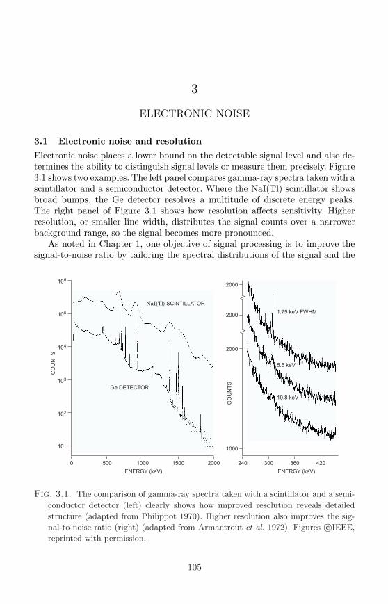
3
ELECTRONIC NOISE
3.1 Electronic noise and resolution
Electronic noise places a lower bound on the detectable signal level and also de-termines the ability to distinguish signal levels or measure them precisely. Figure3.1 shows two examples. The left panel compares gamma-ray spectra taken with ascintillator and a semiconductor detector. Where the NaI(Tl) scintillator showsbroad bumps, the Ge detector resolves a multitude of discrete energy peaks.The right panel of Figure 3.1 shows how resolution affects sensitivity. Higherresolution, or smaller line width, distributes the signal counts over a narrowerbackground range, so the signal becomes more pronounced.
As noted in Chapter 1, one objective of signal processing is to improve thesignal-to-noise ratio by tailoring the spectral distributions of the signal and the
240 300 360 420
ENERGY (keV)
2000
2000
2000
1000
1.75 keV FWHM
5.6 keV
10.8 keV
0 500 1000 1500 2000
ENERGY (keV)
10
10
10
10
10
10
6
5
4
3
2
CO
UN
TS
CO
UN
TS
NaI(Tl) SCINTILLATOR
Ge DETECTOR
Fig. 3.1. The comparison of gamma-ray spectra taken with a scintillator and a semi-
conductor detector (left) clearly shows how improved resolution reveals detailed
structure (adapted from Philippot 1970). Higher resolution also improves the sig-
nal-to-noise ratio (right) (adapted from Armantrout et al. 1972). Figures c©IEEE,
reprinted with permission.
105
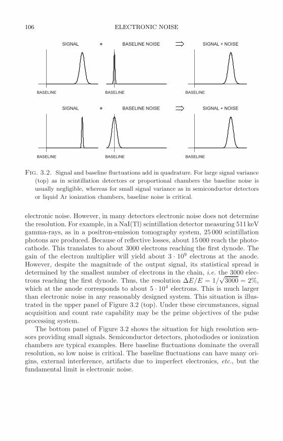
106 ELECTRONIC NOISE
BASELINE
BASELINE
BASELINE
BASELINE
BASELINE
BASELINE
SIGNAL
SIGNAL
BASELINE NOISE
BASELINE NOISE
SIGNAL + NOISE
SIGNAL + NOISE
Fig. 3.2. Signal and baseline fluctuations add in quadrature. For large signal variance
(top) as in scintillation detectors or proportional chambers the baseline noise is
usually negligible, whereas for small signal variance as in semiconductor detectors
or liquid Ar ionization chambers, baseline noise is critical.
electronic noise. However, in many detectors electronic noise does not determinethe resolution. For example, in a NaI(Tl) scintillation detector measuring 511keVgamma-rays, as in a positron-emission tomography system, 25 000 scintillationphotons are produced. Because of reflective losses, about 15 000 reach the photo-cathode. This translates to about 3000 electrons reaching the first dynode. Thegain of the electron multiplier will yield about 3 · 109 electrons at the anode.However, despite the magnitude of the output signal, its statistical spread isdetermined by the smallest number of electrons in the chain, i.e. the 3000 elec-trons reaching the first dynode. Thus, the resolution ∆E/E = 1/
√3000 = 2%,
which at the anode corresponds to about 5 · 104 electrons. This is much largerthan electronic noise in any reasonably designed system. This situation is illus-trated in the upper panel of Figure 3.2 (top). Under these circumstances, signalacquisition and count rate capability may be the prime objectives of the pulseprocessing system.
The bottom panel of Figure 3.2 shows the situation for high resolution sen-sors providing small signals. Semiconductor detectors, photodiodes or ionizationchambers are typical examples. Here baseline fluctuations dominate the overallresolution, so low noise is critical. The baseline fluctuations can have many ori-gins, external interference, artifacts due to imperfect electronics, etc., but thefundamental limit is electronic noise.
ELECTRONIC NOISE 107
3.2 Electronic noise
Consider a current flowing through a sample bounded by two electrodes, i.e. nelectrons moving with velocity v. The induced current depends on the spacing sbetween the electrodes (see “Ramo’s theorem” in Chapter 2), so
i =nev
s. (3.1)
The fluctuation of this current is given by the total differential
〈di〉2 =(ne
s〈dv〉
)2
+(ev
s〈dn〉
)2
, (3.2)
where the two terms add in quadrature, as they are statistically uncorrelated.From this one sees that two mechanisms contribute to the total noise, velocityand number fluctuations.
To evaluate the overall effect of these noise sources in a measurement systemwith a frequency response A(f) we need to know the spectral distribution of thesevarious types of noise. However, before deriving their frequency distributions we’llsimply summarize the results and discuss some general features.
Velocity fluctuations originate from thermal motion. Superimposed on theaverage drift velocity are random velocity fluctuations due to thermal excitation.This “thermal noise” is described by the long wavelength limit of Planck’s blackbody spectrum where the spectral density, i.e. the power per unit bandwidth, isconstant (“white” noise).
Number fluctuations occur in many circumstances. One source is carrier flowthat is limited by emission over a potential barrier. Examples are thermionicemission or current flow in a semiconductor diode. The probability of a carriercrossing the barrier is independent of any other carrier being emitted, so theindividual emissions are random and not correlated. In a reverse-biased diode thecurrent is determined by statistically independent generation and recombinationprocesses (Appendix F). This is called “shot noise”, which also has a “white”spectrum. Another source of number fluctuations is carrier trapping. Impuritiesor imperfections in a crystal lattice can trap charge carriers and release them aftera characteristic lifetime. As shown below, this leads to a frequency-dependentpower spectrum dPn/df = 1/fα, where α is typically in the range of 0.5 – 2.
3.3 Some general properties of noise
Fundamentally, the spectral distribution of noise is described as a power den-sity dPn/df , or in other words, the power in a narrow slice of frequency space.However, in analyzing electronic noise we need to describe the noise in terms ofvoltage and current spectral densities dvn/
√df and din/
√df . In circuit design
literature and data sheets these are commonly abbreviated as dvn/√
df ≡ en anddin/
√df ≡ in, so we’ll follow that convention. This does lead to inconsistencies;
is might represent a signal current with the unit A, whereas in represents a
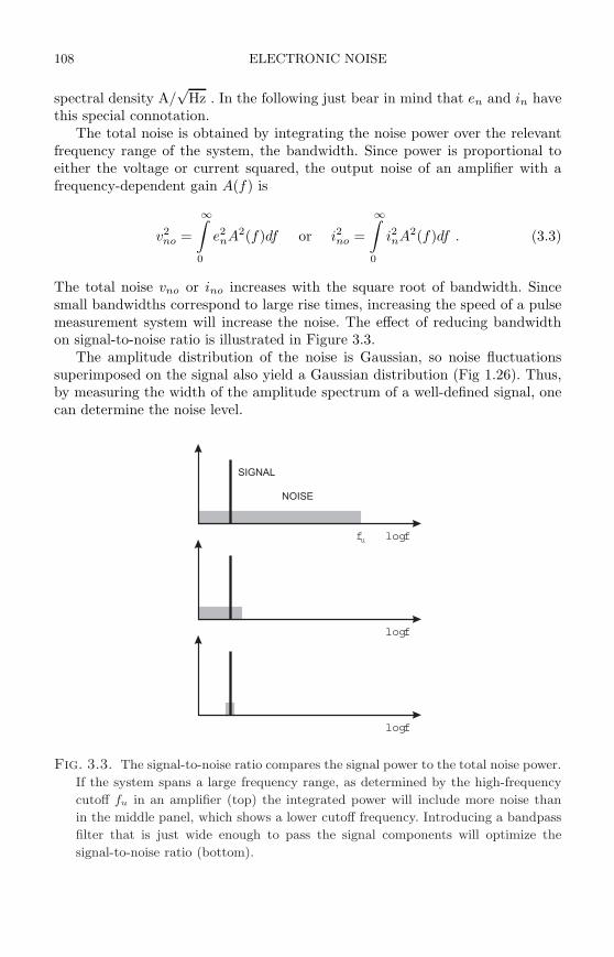
108 ELECTRONIC NOISE
spectral density A/√
Hz . In the following just bear in mind that en and in havethis special connotation.
The total noise is obtained by integrating the noise power over the relevantfrequency range of the system, the bandwidth. Since power is proportional toeither the voltage or current squared, the output noise of an amplifier with afrequency-dependent gain A(f) is
v2no =
∞∫
0
e2nA2(f)df or i2no =
∞∫
0
i2nA2(f)df . (3.3)
The total noise vno or ino increases with the square root of bandwidth. Sincesmall bandwidths correspond to large rise times, increasing the speed of a pulsemeasurement system will increase the noise. The effect of reducing bandwidthon signal-to-noise ratio is illustrated in Figure 3.3.
The amplitude distribution of the noise is Gaussian, so noise fluctuationssuperimposed on the signal also yield a Gaussian distribution (Fig 1.26). Thus,by measuring the width of the amplitude spectrum of a well-defined signal, onecan determine the noise level.
logff
logf
logf
SIGNAL
NOISE
u
Fig. 3.3. The signal-to-noise ratio compares the signal power to the total noise power.
If the system spans a large frequency range, as determined by the high-frequency
cutoff fu in an amplifier (top) the integrated power will include more noise than
in the middle panel, which shows a lower cutoff frequency. Introducing a bandpass
filter that is just wide enough to pass the signal components will optimize the
signal-to-noise ratio (bottom).
SOME GENERAL PROPERTIES OF NOISE 109
First we’ll describe the properties of various types of noise and then derivethe power spectra. More details may be found in books by van der Ziel (1986),for a more theoretical treatment, and by Motchenbacher and Connelly (1993),who take a more practical approach.
3.3.1 Thermal (Johnson) noise
The most common example of noise due to velocity fluctuations is the noise ofresistors. The spectral noise density vs. frequency
dPn
df= 4kT , (3.4)
where k is the Boltzmann constant and T the absolute temperature. Since thepower in a resistance R is
P =v2
R= i2R , (3.5)
the spectral voltage noise density
dv2n
df≡ e2
n = 4kTR (3.6)
and the spectral current noise density
di2ndf
≡ i2n =4kT
R. (3.7)
3.3.2 Shot noise
The spectral noise density of shot noise
i2n = 2eI , (3.8)
where I is the average current and e the electronic charge. Note that the cri-terion for shot noise is that carriers are injected independently of one another,as in thermionic or semiconductor diodes. Current flow determined by an ohmicconductor (I = V/R) does not carry shot noise. Any local fluctuation in elec-tron density relative to the stationary positive charge of the host atoms will setup an electric field that can easily draw in additional carriers to equalize thedisturbance.
3.3.3 Low frequency (“ 1/f”) noise
The noise spectrum becomes nonuniform whenever the fluctuations are notpurely random in time, for example when carriers are trapped and then releasedwith a time constant τ . With an infinite number of uniformly distributed timeconstants the spectral power density assumes a pure 1/f distribution. However,as shown below, with as few as three time constants spread over one or two
110 ELECTRONIC NOISE
decades, the spectrum shows a nearly perfect 1/f distribution over a limitedfrequency range, so this form of noise is very common.
Assume a spectral power density Pnf = Sf/f and a corresponding voltagedensity e2
nf = Af/f . Then the total noise in a frequency band extending fromf1 to f2 is
v2nf =
f2∫
f1
Af
fdf = Af log
(
f2
f1
)
. (3.9)
Thus, for a 1/f spectrum the total noise depends on the ratio of the upper tolower cutoff frequencies, rather than the absolute bandwidth. Since the 1/f dis-tribution refers to the power spectrum, the associated voltage or current spectraldensity changes ten-fold over a 100-fold span in frequency.
3.4 Derivation of spectral densities
3.4.1 Spectral density of thermal noise
Two approaches can be used to derive the spectral distribution of thermal noise:
1. The thermal velocity distribution of the charge carriers is used to calculatethe time dependence of the induced current, which is then transformed intothe frequency domain.
2. Application of Planck’s theory of black-body radiation.
The first approach clearly shows the underlying physics, whereas the second“hides” the physics by applying a general result of statistical mechanics. How-ever, the first requires mathematical tools that go well beyond the standardcurriculum, so the “black-body” approach will be used here.
In Planck’s theory of black body radiation the energy per mode
E =hf
ehf/kT − 1(3.10)
and the spectral density of the radiated power
dP
df=
hf
ehf/kT − 1. (3.11)
This is the power that can be extracted in equilibrium. At low frequencies hf ≪kT the spectral power density
dP
df≈ hf(
1 + hfkT
)
− 1= kT , (3.12)
so the spectral density is independent of frequency and for a total bandwidth Bthe noise power that can be transferred to an external device is Pn = kTB.
DERIVATION OF SPECTRAL DENSITIES 111
RLv
v
i
n
nL
n
R
Fig. 3.4. Equivalent circuit to determine how much thermal noise power can be
extracted from a resistor.
To apply this result to the noise of a resistor, consider a resistance R whosethermal noise gives rise to a noise voltage vn. To determine the power trans-ferred to an external device consider the circuit shown in Figure 3.4. The powerdissipated in the load resistor RL is
v2nL
RL= i2nRL =
v2nRL
(R + RL)2. (3.13)
Maximum power transfers when the load resistance equals the source resistanceRL = R, so
v2nL =
v2n
4. (3.14)
Since the power transferred to RL is kTB,
v2nL
R=
v2n
4R= kTB , (3.15)
Pn =v2
n
R= 4kTB . (3.16)
and the spectral density of the noise power
dPn
df= 4kT . (3.17)
3.4.2 Spectral density of shot noise
When an excess electron is injected into a device, it forms a current pulse ofduration t. In a thermionic diode t is the transit time from cathode to anode,for example. In a forward-biased semiconductor diode t is the recombinationtime (see Appendix E). If these times are short with respect to the periods ofinterest t ≪ 1/f , the current pulse can be represented by a delta pulse. TheFourier transform of a delta pulse yields a “white” spectrum, i.e. the amplitudedistribution in frequency is uniform
din,pk√df
= 2e . (3.18)
112 ELECTRONIC NOISE
Within an infinitesimally narrow frequency band each individual spectral com-ponent is a pure sinusoid, so its rms value
in ≡ din√df
=2e√2
=√
2e . (3.19)
If N electrons are emitted at the same average rate, but at different times, theywill have the same spectral distribution, but the coefficients will differ in phase.For example, for two currents ip and iq with a relative phase ϕ the total rmscurrent is given by
⟨
i2⟩
=(
ip + iqeiϕ) (
ip + iqe−iϕ)
= i2p + i2q + 2ipiq cosϕ . (3.20)
For a random phase the third term averages to zero and
⟨
i2⟩
= i2p + i2q , (3.21)
so if N electrons are randomly emitted per unit time, the individual spectralcomponents simply add in quadrature
i2n = 2Ne2 . (3.22)
The average current I = Ne, so the spectral noise density
i2n ≡ di2ndf
= 2eI . (3.23)
This result can also be obtained by applying Carson’s theorem (van der Ziel1986). If a single pulse has the amplitude A(t) and its Fourier transform
P (f) =
∞∫
−∞
A(t) exp(−iωt)dt , (3.24)
then a random sequence of pulses occurring at a rate r has the spectral powerdistribution
S(f) = 2r |P (f)|2 . (3.25)
Shot noise can be considered as a sequence of delta pulses, which have a whitefrequency spectrum, so the pulse sequence also has a white spectrum. Since therate r = I/e and the integral P (f) = e, the spectral density of shot noise
i2n = 2eI , (3.26)
as derived above in a less general manner. This derivation also demonstratesthat a direct current formed by a random sequence of individual pulses retainsthe spectral distribution of the individual pulses. In other words, the spectraldistribution of a DC signal carries information of the signal’s origin.
DERIVATION OF SPECTRAL DENSITIES 113
0.001 0.01 0.1 1 10 100FREQUENCY (Hz)
10-6
10-5
10-4
10-3
10-2
10-1
100
101
102
dPn/df
= 0.1
= 1
= 0.01
Fig. 3.5. Traps with three time constants of 0.01, 0.1 and 1 s yield a 1/f distribution
over two decades in frequency, although individual traps introduce a 1/f2 spectrum.
A line with a pure 1/f dependence is shown for comparison.
3.4.3 Spectral density of low-frequency noise
Assume a conductor where charge carriers get trapped and subsequently released.This corresponds to a change in conductance ∆G. These events occur indepen-dently in time in a random sequence. Because characteristic times are involved,the shot noise spectrum deviates from white noise in certain frequency ranges.First, let’s consider that all traps have the same lifetime τ . Since this is a formof shot noise, it depends on the magnitude of the current I . The magnitude ofthe excess noise also depends on the conductance G and the number N of trapsin the sample. The spectral density
i2nf = 4NI2
(
∆G
G
)2τ
1 + (ωτ)2. (3.27)
At frequencies well below ω = 2πf = 1/τ the spectrum is white and at highfrequencies well above the corner frequency the spectral density falls off with1/f2. It is not apparent how this can yield a 1/f distribution.
However, it is rare that only a single time constant is involved. With just afew time constants spread over a decade or two, the envelope of the compositespectral density has a 1/f distribution over the corresponding frequency range.This is shown in Figure 3.5, where only three time constants distributed over twodecades in time yield a nearly ideal 1/f response over two decades in frequency.By extension, an infinite number of time constants uniformly distributed yieldsa 1/f spectrum over the full frequency range. Figure 3.5 also illustrates why inpractice 1/f spectra do not extend down to zero frequency. Another unrealisticassumption is that all traps occur at the same concentration. Clearly, reality
114 ELECTRONIC NOISE
doesn’t always follow this pattern, so low frequency noise spectra commonlyshow various regimes with dPn/df = 1/fα, where α is typically in the rangeof 0.5 – 2. Also bear in mind that this is the power density, so when measuringvoltage or current, the magnitude of 1/f noise increases ten-fold over two decadesin frequency.
3.5 “Noiseless” resistances
3.5.1 Dynamic resistances
In many instances a resistance is formed by the slope of a device’s current–voltagecharacteristic, rather than by a static ensemble of electrons agitated by thermalenergy. A common example is a forward-biased semiconductor diode. The diodecurrent vs. voltage (Appendix E)
I = I0(eeV/kT − 1) . (3.28)
The differential resistance
rd =dV
dI=
kT
eI, (3.29)
so at a given current the diode presents a resistance, e.g. 26Ω at I = 1mA andT = 300K.
Note that two diodes can have different charge carrier concentrations, butwill still exhibit the same dynamic resistance at a given current, so the dynamicresistance is not uniquely determined by the number of carriers, as in a resistor.There is no thermal noise associated with this “dynamic” resistance, althoughthe current flow carries shot noise.
3.5.2 Active resistances
In the previous chapter it was shown that the input of an amplifier with capaci-tive feedback can appear resistive. The input resistance is the result of amplifiergain, phase shift, and a feedback capacitor. The feedback capacitor is noiselessfor all practical purposes, since we can ignore vacuum fluctuations. If the am-plifier is noiseless (impossible in reality, but useful as a “thought experiment”),then the input will appear as a noiseless resistance. In practice, the amplifiernoise determines the equivalent noise of the input resistance Ri, but this can bemuch smaller than 4kTRi, so it is equivalent to a “cooled” resistance (Radeka1974). This technique can provide terminations for transmission lines withoutincurring the full thermal noise.
3.5.3 Radiation resistance of an antenna
Consider a receiving antenna with the normalized power pattern Pn(θ, φ) point-ing at a brightness distribution B(θ, φ) in the sky. The power per unit bandwidthreceived by the antenna
dP
df=
Ae
2
∫∫
B(θ, φ)Pn(θ, φ)dΩ (3.30)
CORRELATED NOISE 115
where Ae is the effective aperture, i.e. the “capture area” of the antenna. For agiven field strength E, the captured power P ∝ EAe (Kraus 1986).
If the brightness distribution is from a black-body radiator and we’re mea-suring in the Rayleigh-Jeans regime,
B(θ, φ) =2kT
λ2(3.31)
and the power received by the antenna
dP
df=
kT
λ2AeΩA . (3.32)
ΩA is the beam solid angle of the antenna (measured in rad2), i.e. the anglethrough which all the power would flow if the antenna pattern were uniformover its beamwidth. Since AeΩA = λ2 (see antenna textbooks, for example Kraus1988), the received power
dP
df= kT . (3.33)
The received power is independent of the radiation resistance, as would be ex-pected for thermal noise. However, it is not determined by the temperature of theantenna, but by the temperature of the sky the antenna pattern is subtending.
For example, in a region dominated by the cosmic microwave background,the measured power corresponds to a resistor at a temperature of ∼ 3 K, thoughthe antenna may be at 300K. For a more detailed discussion see Kraus (1986).
3.6 Correlated noise
Generally, noise power is additive:
Pn,tot = Pn1 + Pn1 + . . . (3.34)
However, in a coherent system (i.e. a system that preserves phase), the poweroften results from the sum of voltages or currents, which is sensitive to relativephase.
For two correlated noise sources N1 and N2 the total noise
N2 = N21 + N2
2 + 2CN1N2 , (3.35)
where the correlation coefficient C can range from −1 (anticorrelated, i.e. iden-tical, but 180 out of phase) to +1 (fully correlated). For uncorrelated noisecomponents C = 0 and then individual current or voltage noise contributionsadd in quadrature,
vn,tot =
√
∑
i
v2ni . (3.36)
116 ELECTRONIC NOISE
3.7 Signal equivalent noise measures
The preceding discussion has expressed noise in terms of power and voltage orcurrent. Rather than specifying the noise in absolute terms, it is often moreuseful to express it in terms of the quantity to be measured. The noise level isthen specified as the signal level for which the signal-to-noise ratio equals one.
3.7.1 Noise equivalent power
For example, in a system that measures power, one can express the noise interms of noise equivalent power (NEP), which is equal to the signal input powerfor which the signal-to-noise ratio is one. This measure is commonly used ininfrared and mm-wave measurements. If the signal-to-noise ratio S/N is knownfor a given input power Psignal, the noise equivalent power
NEP =Psignal
(S/N)(3.37)
or, if the noise current and the responsivity (signal current per unit signal power)are known,
NEP =Noise Current
[
A/√
Hz]
Current Responsivity [A/W]. (3.38)
3.7.2 Equivalent noise charge
Similarly, detector readout systems that measure signal charge can be character-ized in terms of equivalent noise charge (ENC), i.e. the signal charge that yieldsa signal-to-noise ratio of one. If absorbed energy yields a signal charge QS anda signal-to-noise ratio S/N , the equivalent noise charge
ENC ≡ Qn =QS
S/N. (3.39)
ENC is commonly expressed in fC or units of the electronic charge e = 1.602 ·10−19 C.
For a given detector material, the signal charge can be translated into ab-sorbed energy, so the noise can be expressed in terms of energy, i.e. eV or keV.For an ionization energy Ei the energy resolution
∆En = Ei · ENC . (3.40)
Equivalent noise charge is the most convenient measure of system noise whendesigning semiconductor detector systems. However, in analyzing the individualnoise contributions, the basic noise parameters – voltage and current – are moreuseful. The combination of individual voltage and current noise contributionstogether with the system bandwidth yields the ENC, so it is a derived, ratherthan a primary quantity.
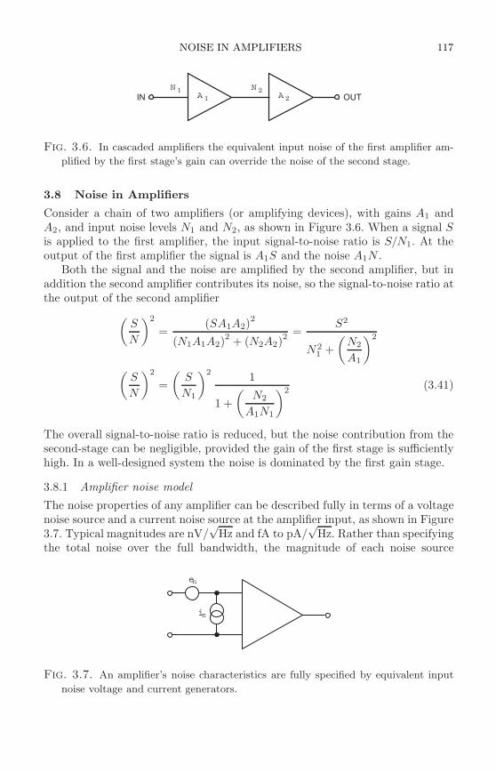
NOISE IN AMPLIFIERS 117
AN N
A1
1 2
2IN OUT
Fig. 3.6. In cascaded amplifiers the equivalent input noise of the first amplifier am-
plified by the first stage’s gain can override the noise of the second stage.
3.8 Noise in Amplifiers
Consider a chain of two amplifiers (or amplifying devices), with gains A1 andA2, and input noise levels N1 and N2, as shown in Figure 3.6. When a signal Sis applied to the first amplifier, the input signal-to-noise ratio is S/N1. At theoutput of the first amplifier the signal is A1S and the noise A1N .
Both the signal and the noise are amplified by the second amplifier, but inaddition the second amplifier contributes its noise, so the signal-to-noise ratio atthe output of the second amplifier
(
S
N
)2
=(SA1A2)
2
(N1A1A2)2
+ (N2A2)2 =
S2
N21 +
(
N2
A1
)2
(
S
N
)2
=
(
S
N1
)21
1 +
(
N2
A1N1
)2 (3.41)
The overall signal-to-noise ratio is reduced, but the noise contribution from thesecond-stage can be negligible, provided the gain of the first stage is sufficientlyhigh. In a well-designed system the noise is dominated by the first gain stage.
3.8.1 Amplifier noise model
The noise properties of any amplifier can be described fully in terms of a voltagenoise source and a current noise source at the amplifier input, as shown in Figure3.7. Typical magnitudes are nV/
√Hz and fA to pA/
√Hz. Rather than specifying
the total noise over the full bandwidth, the magnitude of each noise source
e
i
n
n
Fig. 3.7. An amplifier’s noise characteristics are fully specified by equivalent input
noise voltage and current generators.
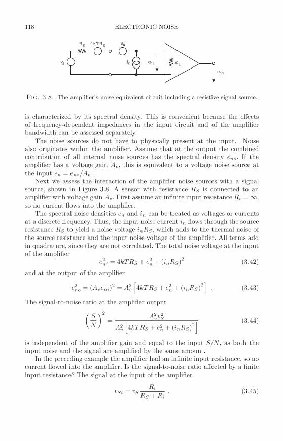
118 ELECTRONIC NOISE
eR 4kTR
Riv e
e
nS S
inS ni
no
Fig. 3.8. The amplifier’s noise equivalent circuit including a resistive signal source.
is characterized by its spectral density. This is convenient because the effectsof frequency-dependent impedances in the input circuit and of the amplifierbandwidth can be assessed separately.
The noise sources do not have to physically present at the input. Noisealso originates within the amplifier. Assume that at the output the combinedcontribution of all internal noise sources has the spectral density eno. If theamplifier has a voltage gain Av, this is equivalent to a voltage noise source atthe input en = eno/Av .
Next we assess the interaction of the amplifier noise sources with a signalsource, shown in Figure 3.8. A sensor with resistance RS is connected to anamplifier with voltage gain Av . First assume an infinite input resistance Ri = ∞,so no current flows into the amplifier.
The spectral noise densities en and in can be treated as voltages or currentsat a discrete frequency. Thus, the input noise current in flows through the sourceresistance RS to yield a noise voltage inRS , which adds to the thermal noise ofthe source resistance and the input noise voltage of the amplifier. All terms addin quadrature, since they are not correlated. The total noise voltage at the inputof the amplifier
e2ni = 4kTRS + e2
n + (inRS)2
(3.42)
and at the output of the amplifier
e2no = (Aveni)
2 = A2v
[
4kTRS + e2n + (inRS)
2]
. (3.43)
The signal-to-noise ratio at the amplifier output
(
S
N
)2
=A2
vv2S
A2v
[
4kTRS + e2n + (inRS)2
] (3.44)
is independent of the amplifier gain and equal to the input S/N , as both theinput noise and the signal are amplified by the same amount.
In the preceding example the amplifier had an infinite input resistance, so nocurrent flowed into the amplifier. Is the signal-to-noise ratio affected by a finiteinput resistance? The signal at the input of the amplifier
vSi = vSRi
RS + Ri. (3.45)
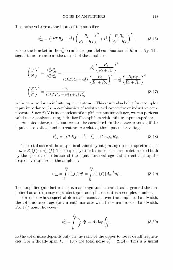
NOISE IN AMPLIFIERS 119
The noise voltage at the input of the amplifier
e2ni =
(
4kTRS + e2n
)
(
Ri
Ri + RS
)2
+ i2n
(
RiRS
Ri + RS
)2
, (3.46)
where the bracket in the i2n term is the parallel combination of Ri and RS . Thesignal-to-noise ratio at the output of the amplifier
(
S
N
)2
=A2
vv2Si
A2ve2
ni
=
v2S
(
Ri
Ri + RS
)2
(4kTRS + e2n)
(
Ri
Ri + RS
)2
+ i2n
(
RiRS
Ri + RS
)2
(
S
N
)2
=v2
S
(4kTRS + e2n) + i2nR2
S
(3.47)
is the same as for an infinite input resistance. This result also holds for a complexinput impedance, i.e. a combination of resistive and capacitive or inductive com-ponents. Since S/N is independent of amplifier input impedance, we can performvalid noise analyses using “idealized” amplifiers with infinite input impedance.
As noted above, noise sources can be correlated. In the above example, if theinput noise voltage and current are correlated, the input noise voltage
e2ni = 4kTRS + e2
n + i2n + 2CeninRS . (3.48)
The total noise at the output is obtained by integrating over the spectral noisepower Pn(f) ∝ e2
no(f). The frequency distribution of the noise is determined bothby the spectral distribution of the input noise voltage and current and by thefrequency response of the amplifier:
v2no =
∞∫
0
e2no(f)df =
∞∫
0
e2ni(f) |Av |2 df . (3.49)
The amplifier gain factor is shown as magnitude squared, as in general the am-plifier has a frequency-dependent gain and phase, so it is a complex number.
For noise whose spectral density is constant over the amplifier bandwidth,the total noise voltage (or current) increases with the square root of bandwidth.For 1/f noise, however,
v2n =
fu∫
fl
Af
fdf = Af log
fu
fl, (3.50)
so the total noise depends only on the ratio of the upper to lower cutoff frequen-cies. For a decade span fu = 10fl the total noise v2
n = 2.3Af . This is a useful
120 ELECTRONIC NOISE
relationship because 1/f noise is often specified as the total noise over one ortwo decades of bandwidth.
Amplifiers commonly exhibit “1/f” noise at low frequencies and white noiseat high frequencies. The “corner frequency” is the frequency where the 1/f noiseequals the white noise, so the 1/f noise is 1/
√2 of the total noise. At f =
fc/100 the 1/f noise voltage is 10 times larger. The corner frequency alone isnot sufficient to specify 1/f noise as it depends on the magnitude of the whitenoise. For the same 1/f noise, a higher white noise level will yield a lower cornerfrequency.
3.8.2 Noise bandwidth vs. signal bandwidth
Consider an amplifier with the frequency response A(f). This can be rewritten
A(f) ≡ A0G(f) (3.51)
where A0 is the maximum gain and G(f) describes the frequency response. Forexample, in the simple amplifier described in Chapter 2 the gain
Av = gm
(
1
RL+ iωCo
)−1
= gmRL1
1 + iωRLCo(3.52)
and using the above convention
A0 ≡ gmRL and G(f) ≡ 1
1 + i(2πfRLCo). (3.53)
If a “white” noise source with spectral density eni is present at the input, thetotal noise voltage at the output is
vno =
√
√
√
√
√
∞∫
0
e2ni |A0G(f)|2df = eniA0
√
√
√
√
√
∞∫
0
G2(f)df ≡ eniA0
√
∆fn . (3.54)
∆fn is the “noise bandwidth”.Note that, in general, the noise bandwidth and the signal bandwidth are not
the same. If the upper cutoff frequency is determined by a single RC time con-stant, as in the “simple amplifier” discussed in Chapter 2, the signal bandwidth
∆fs = fu =1
2πRC(3.55)
and the noise bandwidth
∆fn =1
4RC=
π
2fu . (3.56)
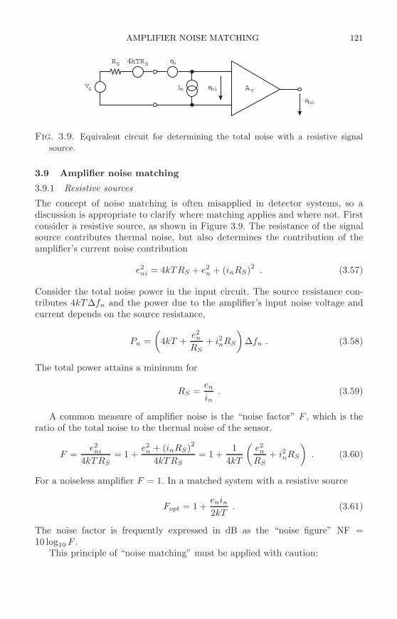
AMPLIFIER NOISE MATCHING 121
eR 4kTR
Aiv e
e
nS S
vnS ni
no
Fig. 3.9. Equivalent circuit for determining the total noise with a resistive signal
source.
3.9 Amplifier noise matching
3.9.1 Resistive sources
The concept of noise matching is often misapplied in detector systems, so adiscussion is appropriate to clarify where matching applies and where not. Firstconsider a resistive source, as shown in Figure 3.9. The resistance of the signalsource contributes thermal noise, but also determines the contribution of theamplifier’s current noise contribution
e2ni = 4kTRS + e2
n + (inRS)2 . (3.57)
Consider the total noise power in the input circuit. The source resistance con-tributes 4kT∆fn and the power due to the amplifier’s input noise voltage andcurrent depends on the source resistance,
Pn =
(
4kT +e2
n
RS+ i2nRS
)
∆fn . (3.58)
The total power attains a minimum for
RS =en
in. (3.59)
A common measure of amplifier noise is the “noise factor” F , which is theratio of the total noise to the thermal noise of the sensor.
F =e2
ni
4kTRS= 1 +
e2n + (inRS)
2
4kTRS= 1 +
1
4kT
(
e2n
RS+ i2nRS
)
. (3.60)
For a noiseless amplifier F = 1. In a matched system with a resistive source
Fopt = 1 +enin2kT
. (3.61)
The noise factor is frequently expressed in dB as the “noise figure” NF =10 log10 F .
This principle of “noise matching” must be applied with caution:
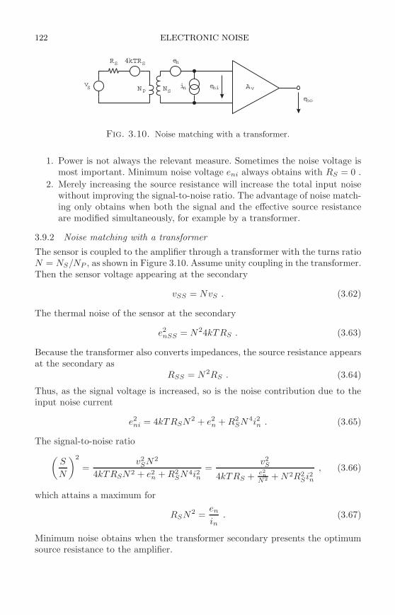
122 ELECTRONIC NOISE
eR
N N
4kTR
Aiv e
e
nS
P S
S
vnS ni
no
Fig. 3.10. Noise matching with a transformer.
1. Power is not always the relevant measure. Sometimes the noise voltage ismost important. Minimum noise voltage eni always obtains with RS = 0 .
2. Merely increasing the source resistance will increase the total input noisewithout improving the signal-to-noise ratio. The advantage of noise match-ing only obtains when both the signal and the effective source resistanceare modified simultaneously, for example by a transformer.
3.9.2 Noise matching with a transformer
The sensor is coupled to the amplifier through a transformer with the turns ratioN = NS/NP , as shown in Figure 3.10. Assume unity coupling in the transformer.Then the sensor voltage appearing at the secondary
vSS = NvS . (3.62)
The thermal noise of the sensor at the secondary
e2nSS = N24kTRS . (3.63)
Because the transformer also converts impedances, the source resistance appearsat the secondary as
RSS = N2RS . (3.64)
Thus, as the signal voltage is increased, so is the noise contribution due to theinput noise current
e2ni = 4kTRSN2 + e2
n + R2SN4i2n . (3.65)
The signal-to-noise ratio
(
S
N
)2
=v2
SN2
4kTRSN2 + e2n + R2
SN4i2n=
v2S
4kTRS +e2
n
N2 + N2R2Si2n
, (3.66)
which attains a maximum for
RSN2 =en
in. (3.67)
Minimum noise obtains when the transformer secondary presents the optimumsource resistance to the amplifier.
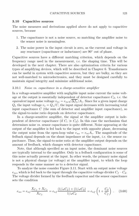
CAPACITIVE SOURCES 123
3.10 Capacitive sources
The noise measures and derivations applied above do not apply to capacitivesources, because
1. The capacitance is not a noise source, so matching the amplifier noise tothe sensor noise is meaningless.
2. The noise power in the input circuit is zero, as the current and voltage inany reactance (capacitance or inductance) are 90 out of phase.
Capacitive sources have a different matching criterion, which depends on thefrequency range used in the measurement, i.e. the shaping time. This will bedeveloped in the next chapter. There are also optimization criteria for varioustypes of amplifying devices, which will be described in Chapter 6. Transformerscan be useful in system with capacitive sources, but they are bulky, so they arenot well-matched to microelectronics, and they must be designed carefully tomaintain signal integrity and minimize additional noise.
3.10.1 Noise vs. capacitance in a charge-sensitive amplifier
In a voltage-sensitive amplifier with negligible input noise current the noise volt-age at the output is essentially independent of detector capacitance Cd, i.e. theequivalent input noise voltage vni = eno
√∆fn/Av. Since for a given input charge
Qs the input voltage vs = Qs/C, the input signal decreases with increasing totalinput capacitance C (the sum of detector and amplifier input capacitance), sothe signal-to-noise ratio depends on detector capacitance.
In a charge-sensitive amplifier, the signal at the amplifier output is inde-pendent of detector capacitance (if Ci ≫ Cd). In this case the mechanism thatdetermines noise vs. sensor capacitance is quite different. Noise appearing at theoutput of the amplifier is fed back to the input with opposite phase, decreasingthe output noise from the open-loop value eno = eniAv . The magnitude of thefedback signal depends on the shunt impedance at the input, i.e. the sensor ca-pacitance. Thus, the signal-to-noise ratio at the amplifier output depends on theamount of feedback, which changes with detector capacitance.
Note, that although specified as an input noise, the dominant noise sourcesare typically internal to the amplifier. Only in a fedback configuration is some ofthis noise actually present at the input. In other words, the primary noise signalis not a physical charge (or voltage) at the amplifier input, to which the loopresponds in the same manner as to a detector signal.
To analyze the noise consider Figure 3.11. Start with an output noise voltageeno, which is fed back to the input through the capacitive voltage divider Cf – Cd.The voltage divider formed by the feedback capacitor and the sensor capacitancesets the condition
eno = enf
XCf+ XCd
XCd
= enf(1/ωCf ) + (1/ωCd)
1/ωCd= enf
(
1 +Cd
Cf
)
. (3.68)
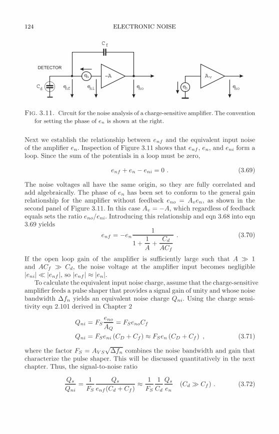
124 ELECTRONIC NOISE
e e e e
C
A A
C nf ni no no
f
v
d
DETECTOR
e
e
n
n
Fig. 3.11. Circuit for the noise analysis of a charge-sensitive amplifier. The convention
for setting the phase of en is shown at the right.
Next we establish the relationship between enf and the equivalent input noiseof the amplifier en. Inspection of Figure 3.11 shows that enf , en, and eni form aloop. Since the sum of the potentials in a loop must be zero,
enf + en − eni = 0 . (3.69)
The noise voltages all have the same origin, so they are fully correlated andadd algebraically. The phase of en has been set to conform to the general gainrelationship for the amplifier without feedback eno = Aven, as shown in thesecond panel of Figure 3.11. In this case Av = −A, which regardless of feedbackequals sets the ratio eno/eni. Introducing this relationship and eqn 3.68 into eqn3.69 yields
enf = −en1
1 +1
A+
Cd
ACf
. (3.70)
If the open loop gain of the amplifier is sufficiently large such that A ≫ 1and ACf ≫ Cd, the noise voltage at the amplifier input becomes negligible|eni| ≪ |enf |, so |enf | ≈ |en|.
To calculate the equivalent input noise charge, assume that the charge-sensitiveamplifier feeds a pulse shaper that provides a signal gain of unity and whose noisebandwidth ∆fn yields an equivalent noise charge Qni. Using the charge sensi-tivity eqn 2.101 derived in Chapter 2
Qni = FSeno
AQ= FSenoCf
Qni = FSeni (CD + Cf ) ≈ FSen (CD + Cf ) , (3.71)
where the factor FS = AV S
√∆fn combines the noise bandwidth and gain that
characterize the pulse shaper. This will be discussed quantitatively in the nextchapter. Thus, the signal-to-noise ratio
Qs
Qni=
1
FS
Qs
enf (Cd + Cf )≈ 1
FS
1
Cd
Qs
en(Cd ≫ Cf ) . (3.72)
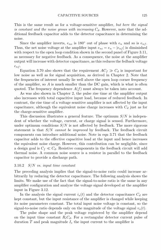
CAPACITIVE SOURCES 125
This is the same result as for a voltage-sensitive amplifier, but here the signalis constant and the noise grows with increasing Cd. However, note that the ad-ditional feedback capacitor adds to the detector capacitance in determining thenoise.
Since the amplifier inverts, eno is 180 out of phase with en and so is enf .Thus, the net noise voltage at the amplifier input eni = en − |enf | is diminishedwith respect to the open loop condition shown in the second panel of Figure 3.11,as necessary for negative feedback. As a consequence, the noise at the amplifieroutput will increase with detector capacitance, as this reduces the fedback voltageenf .
Equation 3.70 also shows that the requirement ACf ≫ Cd is important forlow noise as well as for signal acquisition, as derived in Chapter 2. Note thatthe frequencies of interest usually lie well above the open loop corner frequencyof the amplifier, so A is much smaller than the DC gain, which is what is oftenquoted. The frequency dependence A(f) must always be taken into account.
As was also shown in Chapter 2, the pulse rise time at the amplifier outputalso increases with total capacitive input load, because of reduced feedback. Incontrast, the rise time of a voltage sensitive amplifier is not affected by the inputcapacitance, although the equivalent noise charge increases with Cd just as forthe charge-sensitive amplifier.
This discussion illustrates a general feature. The optimum S/N is indepen-dent of whether the voltage, current, or charge signal is sensed. Furthermore,under optimum conditions S/N is not affected by feedback. The more rigorousstatement is that S/N cannot be improved by feedback. The feedback circuitcomponents can introduce additional noise. Note in eqn 3.71 that the feedbackcapacitor adds to the effective capacitive load at the input and hence increasesthe equivalent noise charge. However, this contribution can be negligible, sincea design goal is Cf ≪ Cd. Resistive components in the feedback circuit will addthermal noise. A common noise source is a resistor in parallel to the feedbackcapacitor to provide a discharge path.
3.10.2 S/N vs. input time constant
The preceding analysis implies that the signal-to-noise ratio could increase ar-bitrarily by reducing the detector capacitance. The following analysis shows thelimits. We make use of the fact that the signal-to-noise ratio is the same in anyamplifier configuration and analyze the voltage signal developed at the amplifierinput in Figure 3.12.
In the analysis the signal current is(t) and the detector capacitance Cd arekept constant, but the input resistance of the amplifier is changed while keepingits noise parameters constant. The total input noise voltage is constant, so thesignal-to-noise ratio depends only on the magnitude of the voltage signal vs(t).
The pulse shape and the peak voltage registered by the amplifier dependon the input time constant RiCd. For a rectangular detector current pulse ofduration T and peak magnitude Is the input current to the amplifier is
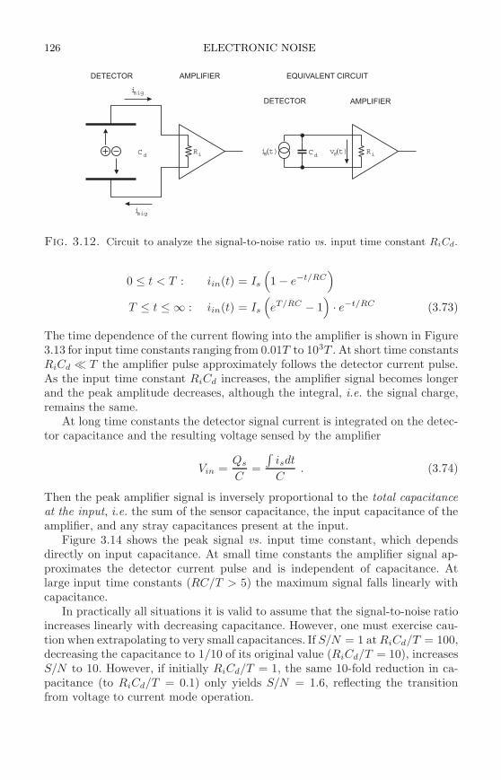
126 ELECTRONIC NOISE
C Cd d
AMPLIFIER
i
i
sig
sig
i v(t) (t)s s RR ii
DETECTOR
DETECTOR AMPLIFIER EQUIVALENT CIRCUIT
Fig. 3.12. Circuit to analyze the signal-to-noise ratio vs. input time constant RiCd.
0 ≤ t < T : iin(t) = Is
(
1 − e−t/RC)
T ≤ t ≤ ∞ : iin(t) = Is
(
eT/RC − 1)
· e−t/RC (3.73)
The time dependence of the current flowing into the amplifier is shown in Figure3.13 for input time constants ranging from 0.01T to 103T . At short time constantsRiCd ≪ T the amplifier pulse approximately follows the detector current pulse.As the input time constant RiCd increases, the amplifier signal becomes longerand the peak amplitude decreases, although the integral, i.e. the signal charge,remains the same.
At long time constants the detector signal current is integrated on the detec-tor capacitance and the resulting voltage sensed by the amplifier
Vin =Qs
C=
∫
isdt
C. (3.74)
Then the peak amplifier signal is inversely proportional to the total capacitanceat the input, i.e. the sum of the sensor capacitance, the input capacitance of theamplifier, and any stray capacitances present at the input.
Figure 3.14 shows the peak signal vs. input time constant, which dependsdirectly on input capacitance. At small time constants the amplifier signal ap-proximates the detector current pulse and is independent of capacitance. Atlarge input time constants (RC/T > 5) the maximum signal falls linearly withcapacitance.
In practically all situations it is valid to assume that the signal-to-noise ratioincreases linearly with decreasing capacitance. However, one must exercise cau-tion when extrapolating to very small capacitances. If S/N = 1 at RiCd/T = 100,decreasing the capacitance to 1/10 of its original value (RiCd/T = 10), increasesS/N to 10. However, if initially RiCd/T = 1, the same 10-fold reduction in ca-pacitance (to RiCd/T = 0.1) only yields S/N = 1.6, reflecting the transitionfrom voltage to current mode operation.
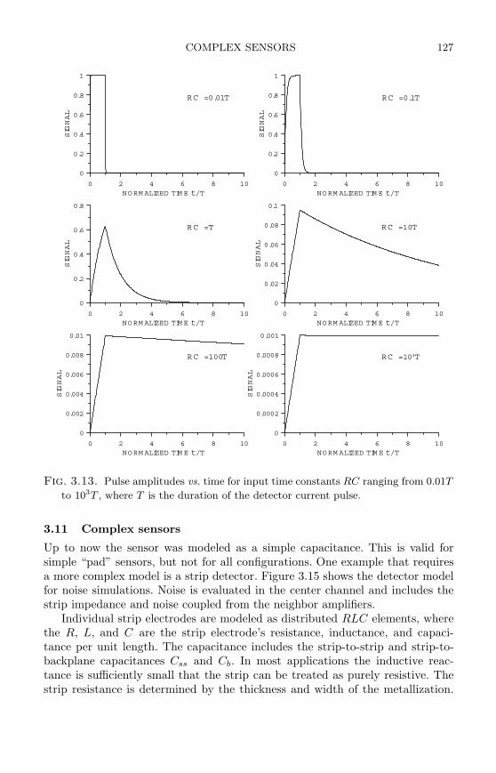
COMPLEX SENSORS 127
0 2 4 6 8 10
NORM ALIZED TIM E t/T
0
0.2
0.4
0.6
0.8
1
SIGNAL
RC = 0.01T
0 2 4 6 8 10
NORM ALIZED TIM E t/T
0
0.2
0.4
0.6
0.8
1
SIGNAL
RC = 0.1T
0 2 4 6 8 10
NORM ALIZED TIM E t/T
0
0.2
0.4
0.6
0.8
SIGNAL
RC = T
0 2 4 6 8 10
NORM ALIZED TIM E t/T
0
0.02
0.04
0.06
0.08
0.1
SIGNAL
RC = 10T
0 2 4 6 8 10
NORM ALIZED TIM E t/T
0
0.002
0.004
0.006
0.008
0.01
SIGNAL
RC = 100T
0 2 4 6 8 10
NORM ALIZED TIM E t/T
0
0.0002
0.0004
0.0006
0.0008
0.001
SIGNAL
RC = 103T
Fig. 3.13. Pulse amplitudes vs. time for input time constants RC ranging from 0.01T
to 103T , where T is the duration of the detector current pulse.
3.11 Complex sensors
Up to now the sensor was modeled as a simple capacitance. This is valid forsimple “pad” sensors, but not for all configurations. One example that requiresa more complex model is a strip detector. Figure 3.15 shows the detector modelfor noise simulations. Noise is evaluated in the center channel and includes thestrip impedance and noise coupled from the neighbor amplifiers.
Individual strip electrodes are modeled as distributed RLC elements, wherethe R, L, and C are the strip electrode’s resistance, inductance, and capaci-tance per unit length. The capacitance includes the strip-to-strip and strip-to-backplane capacitances Css and Cb. In most applications the inductive reac-tance is sufficiently small that the strip can be treated as purely resistive. Thestrip resistance is determined by the thickness and width of the metallization.
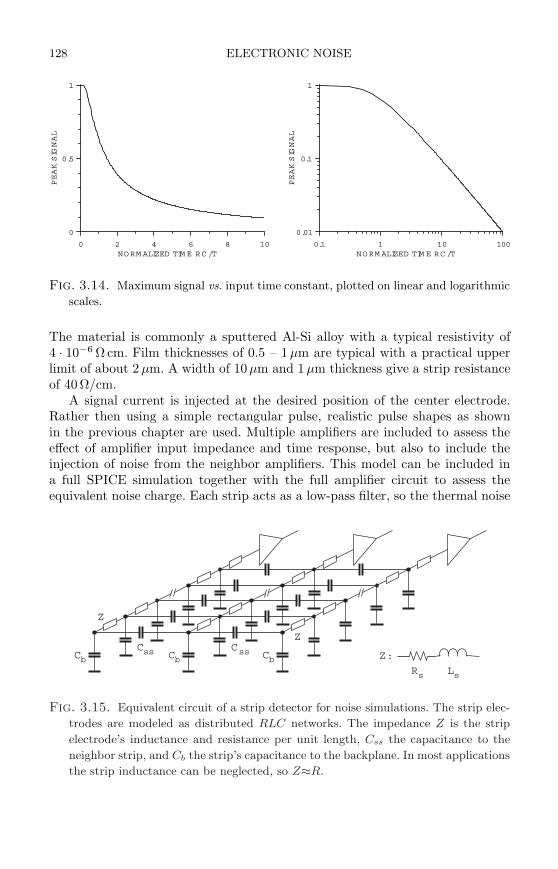
128 ELECTRONIC NOISE
0 2 4 6 8 10NORM ALIZED TIM E RC /T
0
0.5
1
PEAKSIGNAL
0.1 1 10 100NORM ALIZED TIM E RC /T
0.01
0.1
1
PEAKSIGNAL
Fig. 3.14. Maximum signal vs. input time constant, plotted on linear and logarithmic
scales.
The material is commonly a sputtered Al-Si alloy with a typical resistivity of4 · 10−6 Ω cm. Film thicknesses of 0.5 – 1 µm are typical with a practical upperlimit of about 2 µm. A width of 10µm and 1 µm thickness give a strip resistanceof 40Ω/cm.
A signal current is injected at the desired position of the center electrode.Rather then using a simple rectangular pulse, realistic pulse shapes as shownin the previous chapter are used. Multiple amplifiers are included to assess theeffect of amplifier input impedance and time response, but also to include theinjection of noise from the neighbor amplifiers. This model can be included ina full SPICE simulation together with the full amplifier circuit to assess theequivalent noise charge. Each strip acts as a low-pass filter, so the thermal noise
C CC C
R L
Cb bss ss
s s
b
Z
Z
Z:
Fig. 3.15. Equivalent circuit of a strip detector for noise simulations. The strip elec-
trodes are modeled as distributed RLC networks. The impedance Z is the strip
electrode’s inductance and resistance per unit length, Css the capacitance to the
neighbor strip, and Cb the strip’s capacitance to the backplane. In most applications
the strip inductance can be neglected, so Z≈R.
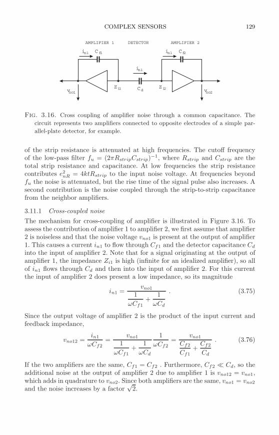
COMPLEX SENSORS 129
v v
CCi
i
i
Z ZCno1 no2
f2f1n1
n1
n1
i1 i2d
DETECTORAMPLIFIER 1 AMPLIFIER 2
Fig. 3.16. Cross coupling of amplifier noise through a common capacitance. The
circuit represents two amplifiers connected to opposite electrodes of a simple par-
allel-plate detector, for example.
of the strip resistance is attenuated at high frequencies. The cutoff frequencyof the low-pass filter fu = (2πRstripCstrip)
−1, where Rstrip and Cstrip are thetotal strip resistance and capacitance. At low frequencies the strip resistancecontributes e2
nR = 4ktRstrip to the input noise voltage. At frequencies beyondfu the noise is attenuated, but the rise time of the signal pulse also increases. Asecond contribution is the noise coupled through the strip-to-strip capacitancefrom the neighbor amplifiers.
3.11.1 Cross-coupled noise
The mechanism for cross-coupling of amplifier is illustrated in Figure 3.16. Toassess the contribution of amplifier 1 to amplifier 2, we first assume that amplifier2 is noiseless and that the noise voltage vno1 is present at the output of amplifier1. This causes a current in1 to flow through Cf1 and the detector capacitance Cd
into the input of amplifier 2. Note that for a signal originating at the output ofamplifier 1, the impedance Zi1 is high (infinite for an idealized amplifier), so allof in1 flows through Cd and then into the input of amplifier 2. For this currentthe input of amplifier 2 does present a low impedance, so its magnitude
in1 =vno1
1
ωCf1+
1
ωCd
. (3.75)
Since the output voltage of amplifier 2 is the product of the input current andfeedback impedance,
vno12 =in1
ωCf2=
vno1
1
ωCf1+
1
ωCd
1
ωCf2=
vno1
Cf2
Cf1+
Cf2
Cd
. (3.76)
If the two amplifiers are the same, Cf1 = Cf2 . Furthermore, Cf2 ≪ Cd, so theadditional noise at the output of amplifier 2 due to amplifier 1 is vno12 = vno1,which adds in quadrature to vno2. Since both amplifiers are the same, vno1 = vno2
and the noise increases by a factor√
2.
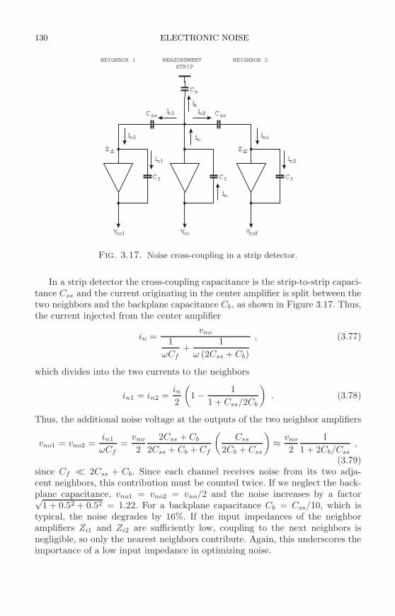
130 ELECTRONIC NOISE
v v v
CC
C
C
ii
i
i
i
i
i i
i
CC
no1 no no2
ff
b
f
n2
b
n
n
n1
n1
n1 n2
n2
ssss
NEIGHBOR 1 NEIGHBOR 2MEASUREMENTSTRIP
Z Zi1 i2
Fig. 3.17. Noise cross-coupling in a strip detector.
In a strip detector the cross-coupling capacitance is the strip-to-strip capaci-tance Css and the current originating in the center amplifier is split between thetwo neighbors and the backplane capacitance Cb, as shown in Figure 3.17. Thus,the current injected from the center amplifier
in =vno
1
ωCf+
1
ω (2Css + Cb)
, (3.77)
which divides into the two currents to the neighbors
in1 = in2 =in2
(
1 − 1
1 + Css/2Cb
)
. (3.78)
Thus, the additional noise voltage at the outputs of the two neighbor amplifiers
vno1 = vno2 =in1
ωCf=
vno
2
2Css + Cb
2Css + Cb + Cf
(
Css
2Cb + Css
)
≈ vno
2
1
1 + 2Cb/Css,
(3.79)since Cf ≪ 2Css + Cb. Since each channel receives noise from its two adja-cent neighbors, this contribution must be counted twice. If we neglect the back-plane capacitance, vno1 = vno2 = vno/2 and the noise increases by a factor√
1 + 0.52 + 0.52 = 1.22. For a backplane capacitance Cb = Css/10, which istypical, the noise degrades by 16%. If the input impedances of the neighboramplifiers Zi1 and Zi2 are sufficiently low, coupling to the next neighbors isnegligible, so only the nearest neighbors contribute. Again, this underscores theimportance of a low input impedance in optimizing noise.
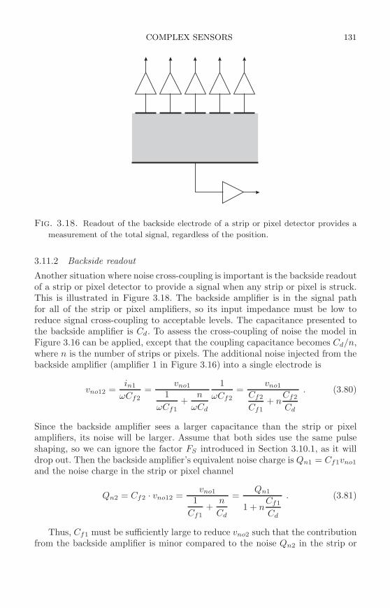
COMPLEX SENSORS 131
Fig. 3.18. Readout of the backside electrode of a strip or pixel detector provides a
measurement of the total signal, regardless of the position.
3.11.2 Backside readout
Another situation where noise cross-coupling is important is the backside readoutof a strip or pixel detector to provide a signal when any strip or pixel is struck.This is illustrated in Figure 3.18. The backside amplifier is in the signal pathfor all of the strip or pixel amplifiers, so its input impedance must be low toreduce signal cross-coupling to acceptable levels. The capacitance presented tothe backside amplifier is Cd. To assess the cross-coupling of noise the model inFigure 3.16 can be applied, except that the coupling capacitance becomes Cd/n,where n is the number of strips or pixels. The additional noise injected from thebackside amplifier (amplifier 1 in Figure 3.16) into a single electrode is
vno12 =in1
ωCf2=
vno1
1
ωCf1+
n
ωCd
1
ωCf2=
vno1
Cf2
Cf1+ n
Cf2
Cd
. (3.80)
Since the backside amplifier sees a larger capacitance than the strip or pixelamplifiers, its noise will be larger. Assume that both sides use the same pulseshaping, so we can ignore the factor FS introduced in Section 3.10.1, as it willdrop out. Then the backside amplifier’s equivalent noise charge is Qn1 = Cf1vno1
and the noise charge in the strip or pixel channel
Qn2 = Cf2 · vno12 =vno1
1
Cf1+
n
Cd
=Qn1
1 + nCf1
Cd
. (3.81)
Thus, Cf1 must be sufficiently large to reduce vno2 such that the contributionfrom the backside amplifier is minor compared to the noise Qn2 in the strip or
132 ELECTRONIC NOISE
pixel channels. Since Qn1 will tend to be larger than Qn2 because of the largercapacitance, this drives feedback capacitor Cf1 to larger values than usual.
Backside readout is often used to derive a timing signal. Since the pixel orstrip amplifiers are in the current return path of the backside amplifier, theirresponse time affects the backside signal. This places a constraint on their inputtime constants, which will tend to be more rigorous than for charge measurementsalone.
3.12 Quantum noise limits in amplifiers
What is the lower limit to electronic noise? Can it be eliminated altogether,for example by using superconductors to eliminate thermal noise and avoidingdevices that carry shot noise? The starting point is the uncertainty relationship
∆E∆t ≥ h
2. (3.82)
Consider a narrow frequency band at frequency ω. The energy uncertainty canbe given in terms of the uncertainty in the number of signal quanta
∆E = hω∆N (3.83)
and the time uncertainty in terms of phase
∆t =∆ϕ
ω, (3.84)
so that
∆ϕ∆N ≥ 1
2. (3.85)
We assume that the distributions in number and phase are Gaussian, so that theequal sign applies.
Next, assume a noiseless amplifier with gain G, so that N1 quanta at theinput yield
N2 = GN1 (3.86)
quanta at the output. Then the output must also obey the relationship
∆ϕ2∆N2 =1
2. (3.87)
However, since ∆N2 = G∆N1 and since the output is shifted by a constant phasewith respect to the input, ∆ϕ2 = ∆ϕ1,
∆ϕ1∆N1 =1
2G, (3.88)
which is smaller than allowed by the uncertainty principle.
REFERENCES 133
This contradiction can only be avoided by assuming that the amplifier intro-duces noise per unit bandwidth of
dPno
dω= (G − 1)hω , (3.89)
which, referred to the input, is
dPni
dω=
(
1 − 1
G
)
hω . (3.90)
If the noise from the following gain stages is to be small, the gain of the firststage must be large, and then the minimum noise of the amplifier is (Haus andMullen 1962)
dPni
dω= hω . (3.91)
The quantum-limited spectral noise density is proportional to frequency. At thefrequencies in the MHz range characteristic of semiconductor detector systems,the quantum noise limit is much below typical noise levels. However, at frequen-cies > 10GHz this is no longer the case.
This minimum noise limit applies only to phase-coherent systems. In systemswhere the phase information is lost, e.g. bolometers, this limit does not apply. At100GHz bolometers exhibit noise levels well below the amplifier quantum noiselimit. For a detailed discussion see Caves (1982).
References
Armantrout, G.A. et al. (1972). Sensitivity problems in biological and environ-mental counting. IEEE Trans. Nucl. Sci. NS-19/1 (1972) 107–116
Caves, C.M. (1982). Quantum limits on noise in linear amplifiers. Phys. Rev.D26 (1982) 1817–1839
Haus, H.A. and Mullen, J.A. (1962). Quantum noise in linear amplifiers. Phys.Rev. 128 (1962) 2407–2413
Kraus, John D. (1986). Radio Astronomy. Cygnus-Quasar Books, Powell, ISBN1-882484-00-2
Kraus, John D. (1988). Antennas (2nd edn). McGraw-Hill, New York, ISBN0-07-035422-7, TK7871.6.K74
Motchenbacher, C.D. and Connelly, J.A. (1993). Low-Noise Electronic SystemDesign. Wiley-Interscience, New York, ISBN 0-471-57742-1, TK7867.M692
Philippot, J.Cl. (1970). Automatic processing of diode spectrometry results.IEEE Trans. Nucl. Sci. NS-17/3 (1970) 446–488
Radeka, V. (1974). Signal, noise and resolution in position-sensitive detectors.IEEE Trans. Nucl. Sci. NS-21 (1974) 51–64
van der Ziel, A. (1986). Noise in Solid State Devices and Circuits. Wiley-Interscience, New York, ISBN 0-471-83234-0, TK7871.85.V34
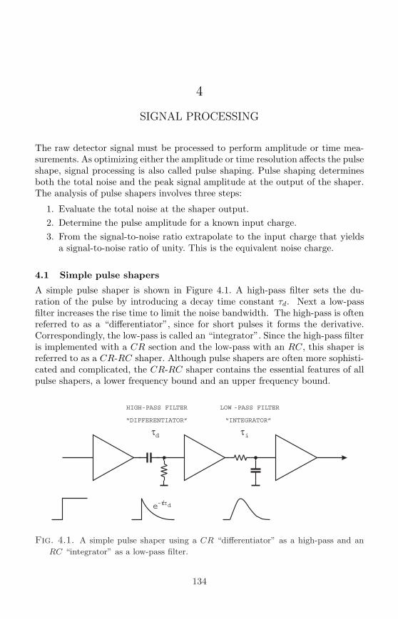
4
SIGNAL PROCESSING
The raw detector signal must be processed to perform amplitude or time mea-surements. As optimizing either the amplitude or time resolution affects the pulseshape, signal processing is also called pulse shaping. Pulse shaping determinesboth the total noise and the peak signal amplitude at the output of the shaper.The analysis of pulse shapers involves three steps:
1. Evaluate the total noise at the shaper output.
2. Determine the pulse amplitude for a known input charge.
3. From the signal-to-noise ratio extrapolate to the input charge that yieldsa signal-to-noise ratio of unity. This is the equivalent noise charge.
4.1 Simple pulse shapers
A simple pulse shaper is shown in Figure 4.1. A high-pass filter sets the du-ration of the pulse by introducing a decay time constant τd. Next a low-passfilter increases the rise time to limit the noise bandwidth. The high-pass is oftenreferred to as a “differentiator”, since for short pulses it forms the derivative.Correspondingly, the low-pass is called an “integrator”. Since the high-pass filteris implemented with a CR section and the low-pass with an RC, this shaper isreferred to as a CR-RC shaper. Although pulse shapers are often more sophisti-cated and complicated, the CR-RC shaper contains the essential features of allpulse shapers, a lower frequency bound and an upper frequency bound.
d i
HIGH-PASS FILTER
“DIFFERENTIATOR”
LOW -PASS FILTER
“INTEGRATOR”
e-t/d
Fig. 4.1. A simple pulse shaper using a CR “differentiator” as a high-pass and an
RC “integrator” as a low-pass filter.
134
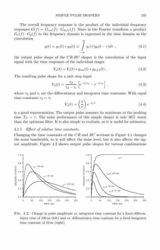
SIMPLE PULSE SHAPERS 135
The overall frequency response is the product of the individual frequencyresponses G(f) = Gint(f) · Gdiff (f). Since in the Fourier transform a productG1(f) · G2(f) in the frequency domain is expressed in the time domain as theconvolution
g(t) = g1(t) ∗ g2(t) ≡∞∫
−∞
g1(τ)g2(t − τ)dτ , (4.1)
the output pulse shape of the CR-RC shaper is the convolution of the inputsignal with the time responses of the individual stages
Vo(t) = Vi(t) ∗ gint(t) ∗ gdiff (t) . (4.2)
The resulting pulse shape for a unit step input
Vo(t) =τd
τd − τi
[
e−t/τd − e−t/τi
]
, (4.3)
where τd and τi are the differentiator and integrator time constants. With equaltime constants τd = τi
Vo(t) =
(
t
τ
)
e−t/τ (4.4)
is a good representation. The output pulse assumes its maximum at the peakingtime TP = τ . The noise performance of this simple shaper is only 36% worsethan the optimum filter. It is also simple to evaluate, so it is useful for estimates.
4.1.1 Effect of relative time constants
Changing the time constants of the CR and RC sections in Figure 4.1 changesthe noise bandwidth, so it will affect the noise level, but it also affects the sig-nal amplitude. Figure 4.2 shows output pulse shapes for various combinations
0 50 100 150 200 250 300
TIM E (ns)
0.0
0.2
0.4
0.6
0.8
1.0
SHAPEROUTPUT
diff =
diff = 100 ns
diff = 30 ns
diff = 10 ns
0 50 100 150 200 250 300
TIM E (ns)
0.0
0.2
0.4
0.6
0.8
1.0
SHAPEROUTPUT int = 10 ns
int = 30 ns
int = 100 ns
Fig. 4.2. Change in pulse amplitude vs. integrator time constant for a fixed differen-
tiator time of 100 ns (left) and vs. differentiator time constant for a fixed integrator
time constant of 10 ns (right).
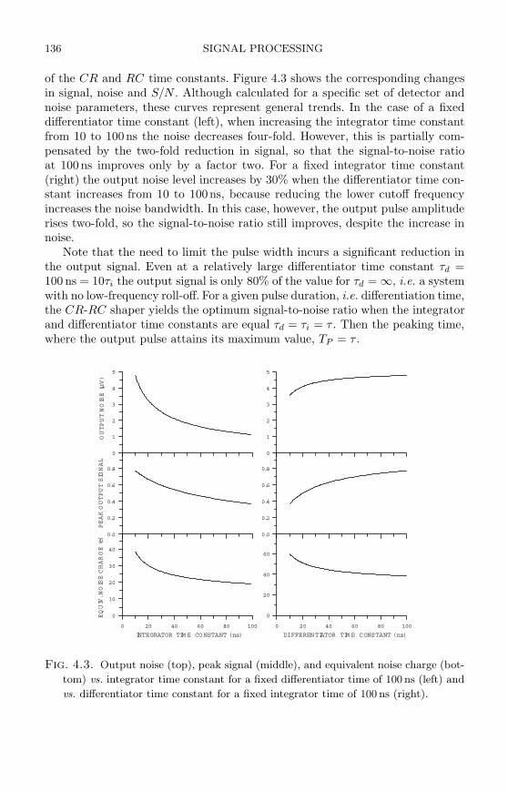
136 SIGNAL PROCESSING
of the CR and RC time constants. Figure 4.3 shows the corresponding changesin signal, noise and S/N . Although calculated for a specific set of detector andnoise parameters, these curves represent general trends. In the case of a fixeddifferentiator time constant (left), when increasing the integrator time constantfrom 10 to 100ns the noise decreases four-fold. However, this is partially com-pensated by the two-fold reduction in signal, so that the signal-to-noise ratioat 100ns improves only by a factor two. For a fixed integrator time constant(right) the output noise level increases by 30% when the differentiator time con-stant increases from 10 to 100ns, because reducing the lower cutoff frequencyincreases the noise bandwidth. In this case, however, the output pulse amplituderises two-fold, so the signal-to-noise ratio still improves, despite the increase innoise.
Note that the need to limit the pulse width incurs a significant reduction inthe output signal. Even at a relatively large differentiator time constant τd =100 ns = 10τi the output signal is only 80% of the value for τd = ∞, i.e. a systemwith no low-frequency roll-off. For a given pulse duration, i.e. differentiation time,the CR-RC shaper yields the optimum signal-to-noise ratio when the integratorand differentiator time constants are equal τd = τi = τ . Then the peaking time,where the output pulse attains its maximum value, TP = τ .
0
1
2
3
4
5
OUTPUTNOISE(µV)
0.0
0.2
0.4
0.6
0.8
PEAKOUTPUTSIGNAL
0 20 40 60 80 100
INTEGRATOR TIM E CO NSTANT (ns)
0
10
20
30
40
EQUIV.NOISECHARGE(e)
0
1
2
3
4
5
0.0
0.2
0.4
0.6
0.8
0 20 40 60 80 100
DIFFERENTIATOR TIM E CONSTANT (ns)
0
20
40
60
Fig. 4.3. Output noise (top), peak signal (middle), and equivalent noise charge (bot-
tom) vs. integrator time constant for a fixed differentiator time of 100 ns (left) and
vs. differentiator time constant for a fixed integrator time of 100 ns (right).
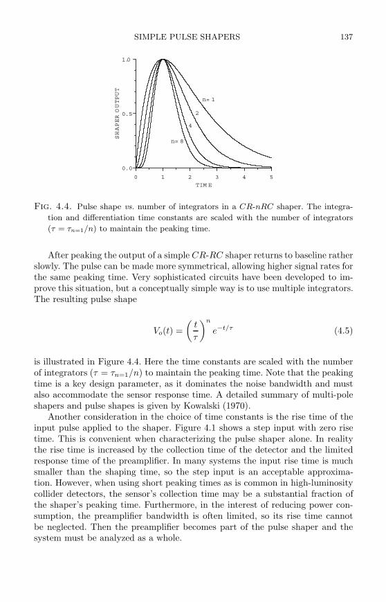
SIMPLE PULSE SHAPERS 137
0 1 2 3 4 5
TIM E
0.0
0.5
1.0
SHAPEROUTPUT
n= 1
2
4
n= 8
Fig. 4.4. Pulse shape vs. number of integrators in a CR-nRC shaper. The integra-
tion and differentiation time constants are scaled with the number of integrators
(τ = τn=1/n) to maintain the peaking time.
After peaking the output of a simple CR-RC shaper returns to baseline ratherslowly. The pulse can be made more symmetrical, allowing higher signal rates forthe same peaking time. Very sophisticated circuits have been developed to im-prove this situation, but a conceptually simple way is to use multiple integrators.The resulting pulse shape
Vo(t) =
(
t
τ
)n
e−t/τ (4.5)
is illustrated in Figure 4.4. Here the time constants are scaled with the numberof integrators (τ = τn=1/n) to maintain the peaking time. Note that the peakingtime is a key design parameter, as it dominates the noise bandwidth and mustalso accommodate the sensor response time. A detailed summary of multi-poleshapers and pulse shapes is given by Kowalski (1970).
Another consideration in the choice of time constants is the rise time of theinput pulse applied to the shaper. Figure 4.1 shows a step input with zero risetime. This is convenient when characterizing the pulse shaper alone. In realitythe rise time is increased by the collection time of the detector and the limitedresponse time of the preamplifier. In many systems the input rise time is muchsmaller than the shaping time, so the step input is an acceptable approxima-tion. However, when using short peaking times as is common in high-luminositycollider detectors, the sensor’s collection time may be a substantial fraction ofthe shaper’s peaking time. Furthermore, in the interest of reducing power con-sumption, the preamplifier bandwidth is often limited, so its rise time cannotbe neglected. Then the preamplifier becomes part of the pulse shaper and thesystem must be analyzed as a whole.
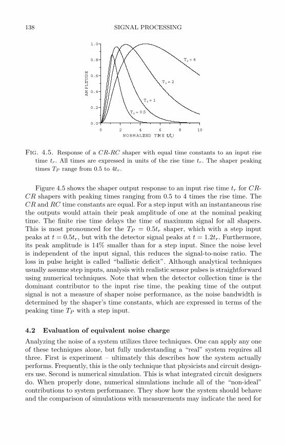
138 SIGNAL PROCESSING
0 2 4 6 8 10
NORM ALIZED TIM E (t/tr)
0.0
0.2
0.4
0.6
0.8
1.0
AMPLITUDE
TP = 0.5
TP = 1
TP = 2
TP = 4
Fig. 4.5. Response of a CR-RC shaper with equal time constants to an input rise
time tr. All times are expressed in units of the rise time tr. The shaper peaking
times TP range from 0.5 to 4tr.
Figure 4.5 shows the shaper output response to an input rise time tr for CR-CR shapers with peaking times ranging from 0.5 to 4 times the rise time. TheCR and RC time constants are equal. For a step input with an instantaneous risethe outputs would attain their peak amplitude of one at the nominal peakingtime. The finite rise time delays the time of maximum signal for all shapers.This is most pronounced for the TP = 0.5tr shaper, which with a step inputpeaks at t = 0.5tr, but with the detector signal peaks at t = 1.2tr. Furthermore,its peak amplitude is 14% smaller than for a step input. Since the noise levelis independent of the input signal, this reduces the signal-to-noise ratio. Theloss in pulse height is called “ballistic deficit”. Although analytical techniquesusually assume step inputs, analysis with realistic sensor pulses is straightforwardusing numerical techniques. Note that when the detector collection time is thedominant contributor to the input rise time, the peaking time of the outputsignal is not a measure of shaper noise performance, as the noise bandwidth isdetermined by the shaper’s time constants, which are expressed in terms of thepeaking time TP with a step input.
4.2 Evaluation of equivalent noise charge
Analyzing the noise of a system utilizes three techniques. One can apply any oneof these techniques alone, but fully understanding a “real” system requires allthree. First is experiment – ultimately this describes how the system actuallyperforms. Frequently, this is the only technique that physicists and circuit design-ers use. Second is numerical simulation. This is what integrated circuit designersdo. When properly done, numerical simulations include all of the “non-ideal”contributions to system performance. They show how the system should behaveand the comparison of simulations with measurements may indicate the need for
EVALUATION OF EQUIVALENT NOISE CHARGE 139
troubleshooting. Finally, the third technique is analytical simulation. Unlike thefirst two techniques, this provides an understanding of how individual compo-nents contribute and points the way for optimizations to be verified by numericalsimulations and measurements.
4.2.1 Experiment
Inject an input signal with known charge using a pulse generator set to ap-proximate the shape of the detector signal (to include possible ballistic deficit).Measure the pulse height spectrum using a multichannel pulse height analyzer.The peak centroid yields the signal magnitude and the peak width yields thenoise (FWHM = 2.35Qn rms)
If pulse-height digitization is not practical, one can measure total noise atthe output of the pulse shaper using an rms voltmeter, a spectrum analyzer, oran oscilloscope. All of these techniques require some attention to proper instru-mentation and measurement techniques.
1. Measure the noise level.
(a) Voltmeter: The voltmeter must have adequate sensitivity and a suffi-ciently large bandwidth to include the full noise spectrum. Most high-frequency voltmeters measure peak amplitude, although the scalereads rms The rms reading is only correct for sinusoidal signals, wherethe peak-to-rms ratio is known. For a Gaussian distribution the peakreading depends on the averaging time, which is not always known.Since measuring the total noise of a spectral distribution requires in-tegrating over the noise power, the correct instrument is a “true rms”voltmeter, which uses thermal sensors or electronically squares theinput signal and displays the square root. Many true rms voltmetersare designed for low-frequency applications, so it is important to ver-ify that the bandwidth is adequate; preferably the rated bandwidthextends well beyond the upper frequency cutoff of the system. It alsodoesn’t hurt to read the operation manual. This is a broadband mea-surement, so it is prone to extraneous signals. Pulse shapers are oftensensitive to frequencies commonly used for radio and television trans-mitters or industrial RF generators. Contamination by these signalswill increase the measured value (see Chapter 9).
(b) Spectrum analyzer: A spectrum analyzer shows the distribution of thenoise vs. frequency and is a powerful diagnostic tool. Signals from ra-dio or TV stations and RF generators appear as discrete peaks in thespectrum and can be eliminated from the digitized output. Again, itis important to verify that the analyzer measures true rms The spec-trum analyzer provides discrete measurement values in N frequencybins ∆fn. Since the measured noise level depends on the resolutionbandwidth, one must also verify that the indicated bandwidth is the
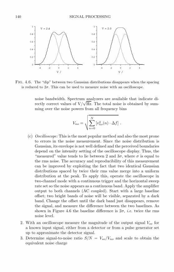
140 SIGNAL PROCESSING
-4 -2 0 2 4
V /
0
0.2
0.4
0.6
0.8
1
-4 -2 0 2 4
V /
0
0.2
0.4
0.6
0.8
1V = 2.4 V = 2.0
Fig. 4.6. The “dip” between two Gaussian distributions disappears when the spacing
is reduced to 2σ. This can be used to measure noise with an oscilloscope.
noise bandwidth. Spectrum analyzers are available that indicate di-rectly correct values of V/
√Hz. The total noise is obtained by sum-
ming over the noise powers from all frequency bins
Vno =
√
√
√
√
N∑
n=0
[v2no(n) · ∆f ] .
(c) Oscilloscope: This is the most popular method and also the most proneto errors in the noise measurement. Since the noise distribution isGaussian, its envelope is not well defined and the perceived boundariesdepend on the intensity setting of the oscilloscope display. Thus, the“measured” value tends to lie between 2 and 3σ, where σ is equal tothe rms noise. The accuracy and reproducibility of this measurementcan be improved by exploiting the fact that two identical Gaussiandistributions spaced by twice their rms value merge into a uniformdistribution at the peak. To apply this, operate the oscilloscope intwo-channel mode with a continuous trigger and the horizontal sweeprate set so the noise appears as a continuous band. Apply the amplifieroutput to both channels (AC coupled). Start with a large baselineoffset; two bright bands of noise will be visible, separated by a darkband. Change the offset until the dark band just disappears, removethe signal, and measure the difference between the two baselines. Asshown in Figure 4.6 the baseline difference is 2σ, i.e. twice the rmsnoise level.
2. With an oscilloscope measure the magnitude of the output signal Vso fora known input signal, either from a detector or from a pulse generator setup to approximate the detector signal.
3. Determine signal-to-noise ratio S/N = Vso/Vno and scale to obtain theequivalent noise charge
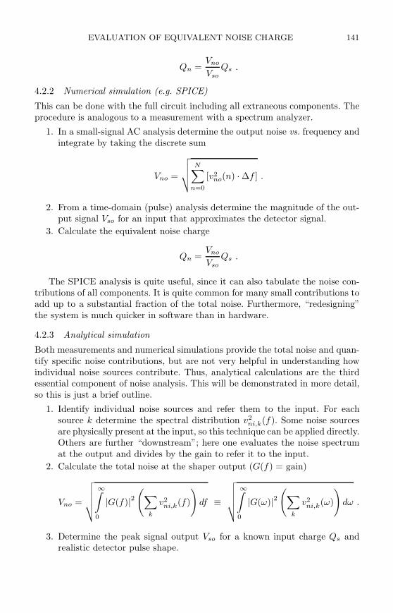
EVALUATION OF EQUIVALENT NOISE CHARGE 141
Qn =Vno
VsoQs .
4.2.2 Numerical simulation (e.g. SPICE)
This can be done with the full circuit including all extraneous components. Theprocedure is analogous to a measurement with a spectrum analyzer.
1. In a small-signal AC analysis determine the output noise vs. frequency andintegrate by taking the discrete sum
Vno =
√
√
√
√
N∑
n=0
[v2no(n) · ∆f ] .
2. From a time-domain (pulse) analysis determine the magnitude of the out-put signal Vso for an input that approximates the detector signal.
3. Calculate the equivalent noise charge
Qn =Vno
VsoQs .
The SPICE analysis is quite useful, since it can also tabulate the noise con-tributions of all components. It is quite common for many small contributions toadd up to a substantial fraction of the total noise. Furthermore, “redesigning”the system is much quicker in software than in hardware.
4.2.3 Analytical simulation
Both measurements and numerical simulations provide the total noise and quan-tify specific noise contributions, but are not very helpful in understanding howindividual noise sources contribute. Thus, analytical calculations are the thirdessential component of noise analysis. This will be demonstrated in more detail,so this is just a brief outline.
1. Identify individual noise sources and refer them to the input. For eachsource k determine the spectral distribution v2
ni,k(f). Some noise sourcesare physically present at the input, so this technique can be applied directly.Others are further “downstream”; here one evaluates the noise spectrumat the output and divides by the gain to refer it to the input.
2. Calculate the total noise at the shaper output (G(f) = gain)
Vno =
√
√
√
√
√
∞∫
0
|G(f)|2(
∑
k
v2ni,k(f)
)
df ≡
√
√
√
√
√
∞∫
0
|G(ω)|2(
∑
k
v2ni,k(ω)
)
dω .
3. Determine the peak signal output Vso for a known input charge Qs andrealistic detector pulse shape.
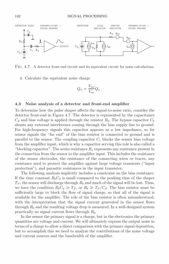
142 SIGNAL PROCESSING
DETECTOR BIASRESISTOR
SERIESRESISTOR
PREAMPLIFIER +PULSE SHAPER
PREAMPLIFIER +PULSE SHAPER
Rs
ii i
e
e
nd
nb na
ns
na
OUTPUT
R
R
b
bCc Rs
Cb
C
C
d
d
DETECTOR BIAS
Fig. 4.7. A detector front-end circuit and its equivalent circuit for noise calculations.
4. Calculate the equivalent noise charge
Qn =Vno
VsoQs .
4.3 Noise analysis of a detector and front-end amplifier
To determine how the pulse shaper affects the signal-to-noise ratio, consider thedetector front-end in Figure 4.7. The detector is represented by the capacitanceCd and bias voltage is applied through the resistor Rb. The bypass capacitor Cb
shunts any external interference coming through the bias supply line to ground.For high-frequency signals this capacitor appears as a low impedance, so forsensor signals the “far end” of the bias resistor is connected to ground and isparallel to the sensor. The coupling capacitor Cc blocks the sensor bias voltagefrom the amplifier input, which is why a capacitor serving this role is also called a“blocking capacitor”. The series resistance Rs represents any resistance present inthe connection from the sensor to the amplifier input. This includes the resistanceof the sensor electrodes, the resistance of the connecting wires or traces, anyresistance used to protect the amplifier against large voltage transients (“inputprotection”), and parasitic resistances in the input transistor.
The following analysis implicitly includes a constraint on the bias resistance.If the time constant RbCd is small compared to the peaking time of the shaperTP , the sensor will discharge through Rb and much of the signal will be lost. Thus,we have the condition RbCd ≫ TP , or Rb ≫ TP /Cd. The bias resistor must besufficiently large to block the flow of signal charge, so that all of the signal isavailable for the amplifier. The role of the bias resistor is often misunderstood,with the interpretation that the signal current generated in the sensor flowsthrough Rb and the resulting voltage drop is measured. In a well-designed systempractically no signal current flows through Rb.
In the sensor the primary signal is a charge, but in the electronics the primaryquantities are voltage and current. We will ultimately express the output noise interms of a charge to allow a direct comparison with the primary signal deposition,but to accomplish this we need to analyze the contributions of the noise voltageand current sources and the bandwidth of the amplifier.
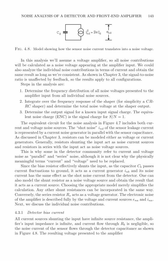
NOISE ANALYSIS OF A DETECTOR AND FRONT-END AMPLIFIER 143
Cd end2e dIind2=
Fig. 4.8. Model showing how the sensor noise current translates into a noise voltage.
In this analysis we’ll assume a voltage amplifier, so all noise contributionswill be calculated as a noise voltage appearing at the amplifier input. We couldalso analyze the individual noise contributions in terms of current and obtain thesame result as long as we’re consistent. As shown in Chapter 3, the signal-to-noiseratio is unaffected by feedback, so the results apply to all configurations.
Steps in the analysis are:
1. Determine the frequency distribution of all noise voltages presented to theamplifier input from all individual noise sources.
2. Integrate over the frequency response of the shaper (for simplicity a CR-RC shaper) and determine the total noise voltage at the shaper output.
3. Determine the output signal for a known input signal charge. The equiva-lent noise charge (ENC) is the signal charge for S/N = 1.
The equivalent circuit for the noise analysis in Figure 4.7 includes both cur-rent and voltage noise sources. The “shot noise” ind of the sensor leakage currentis represented by a current noise generator in parallel with the sensor capacitance.As discussed in Chapter 3, resistors can be modeled either as voltage or currentgenerators. Generally, resistors shunting the input act as noise current sourcesand resistors in series with the input act as noise voltage sources.
This is why some in the detector community refer to current and voltagenoise as “parallel” and “series” noise, although it is not clear why the physicallymeaningful terms “current” and “voltage” need to be replaced.
Since the bias resistor effectively shunts the input, as the capacitor Cb passescurrent fluctuations to ground, it acts as a current generator inb and its noisecurrent has the same effect as the shot noise current from the detector. One canalso model the shunt resistor as a noise voltage source and obtain the result thatit acts as a current source. Choosing the appropriate model merely simplifies thecalculation. Any other shunt resistances can be incorporated in the same way.Conversely, the series resistor Rs acts as a voltage generator. The electronic noiseof the amplifier is described fully by the voltage and current sources ena and ina.Next, we discuss the individual noise contributions.
4.3.1 Detector bias current
All current sources shunting the input have infinite source resistance, the ampli-fier’s input impedance is infinite, and current flow through Rb is negligible, sothe noise current of the sensor flows through the detector capacitance as shownin Figure 4.8. The resulting voltage presented to the amplifier
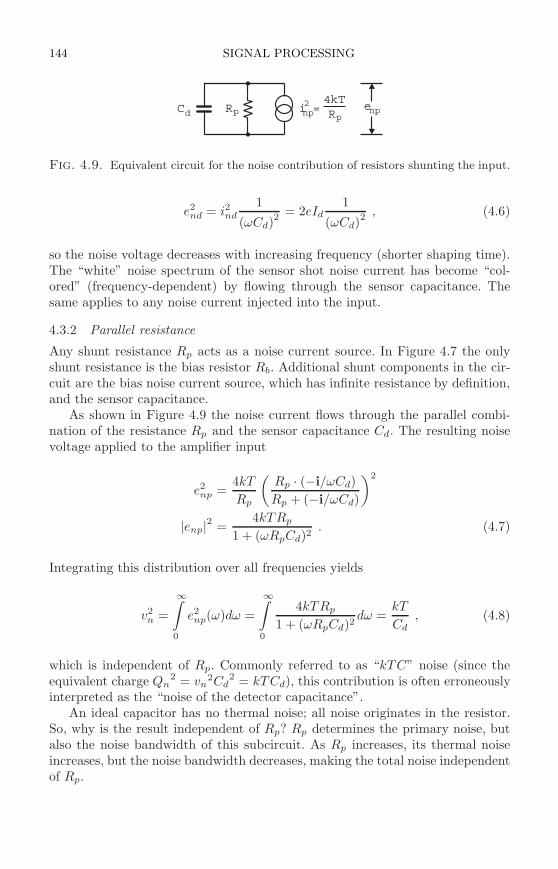
144 SIGNAL PROCESSING
Cd R Rpp
4kTenpinp
2 =
Fig. 4.9. Equivalent circuit for the noise contribution of resistors shunting the input.
e2nd = i2nd
1
(ωCd)2 = 2eId
1
(ωCd)2 , (4.6)
so the noise voltage decreases with increasing frequency (shorter shaping time).The “white” noise spectrum of the sensor shot noise current has become “col-ored” (frequency-dependent) by flowing through the sensor capacitance. Thesame applies to any noise current injected into the input.
4.3.2 Parallel resistance
Any shunt resistance Rp acts as a noise current source. In Figure 4.7 the onlyshunt resistance is the bias resistor Rb. Additional shunt components in the cir-cuit are the bias noise current source, which has infinite resistance by definition,and the sensor capacitance.
As shown in Figure 4.9 the noise current flows through the parallel combi-nation of the resistance Rp and the sensor capacitance Cd. The resulting noisevoltage applied to the amplifier input
e2np =
4kT
Rp
(
Rp · (−i/ωCd)
Rp + (−i/ωCd)
)2
|enp|2 =4kTRp
1 + (ωRpCd)2. (4.7)
Integrating this distribution over all frequencies yields
v2n =
∞∫
0
e2np(ω)dω =
∞∫
0
4kTRp
1 + (ωRpCd)2dω =
kT
Cd, (4.8)
which is independent of Rp. Commonly referred to as “kTC” noise (since theequivalent charge Qn
2 = vn2Cd
2 = kTCd), this contribution is often erroneouslyinterpreted as the “noise of the detector capacitance”.
An ideal capacitor has no thermal noise; all noise originates in the resistor.So, why is the result independent of Rp? Rp determines the primary noise, butalso the noise bandwidth of this subcircuit. As Rp increases, its thermal noiseincreases, but the noise bandwidth decreases, making the total noise independentof Rp.
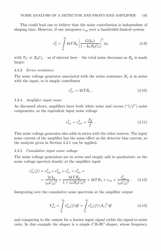
NOISE ANALYSIS OF A DETECTOR AND FRONT-END AMPLIFIER 145
This could lead one to believe that the noise contribution is independent ofshaping time. However, if one integrates enp over a bandwidth-limited system
v2n =
∞∫
0
4kTRp
∣
∣
∣
∣
G(iω)
1 − iωRpCd
∣
∣
∣
∣
2
dω (4.9)
with TP ≪ RpCd – as of interest here – the total noise decreases as Rp is madelarger.
4.3.3 Series resistance
The noise voltage generator associated with the series resistance Rs is in serieswith the input, so it simply contributes
e2nr = 4kTRs . (4.10)
4.3.4 Amplifier input noise
As discussed above, amplifiers have both white noise and excess (“1/f”) noisecomponents, so the equivalent input noise voltage
e2na = e2
nw +Af
f. (4.11)
This noise voltage generator also adds in series with the other sources. The inputnoise current of the amplifier has the same effect as the detector bias current, sothe analysis given in Section 4.3.1 can be applied.
4.3.5 Cumulative input noise voltage
The noise voltage generators are in series and simply add in quadrature, so thenoise voltage spectral density at the amplifier input
e2ni(f) = e2
nd + e2np + e2
nr + e2na =
=2eId
(ωCd)2 +
4kTRp
1 + (ωRpCd)2+ 4kTRs + ena +
i2na
(ωCd)2 . (4.12)
Integrating over the cumulative noise spectrum at the amplifier output
V 2no =
∞∫
0
e2no(f)df =
∞∫
0
e2ni(f) |Av |2 df (4.13)
and comparing to the output for a known input signal yields the signal-to-noiseratio. In this example the shaper is a simple CR-RC shaper, whose frequency
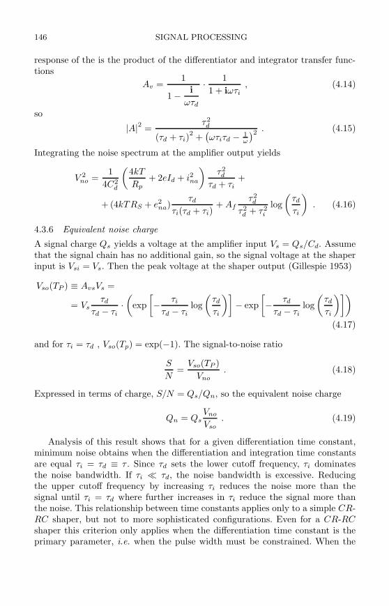
146 SIGNAL PROCESSING
response of the is the product of the differentiator and integrator transfer func-tions
Av =1
1 − i
ωτd
· 1
1 + iωτi, (4.14)
so
|A|2 =τ2d
(τd + τi)2
+(
ωτiτd − 1ω
)2 . (4.15)
Integrating the noise spectrum at the amplifier output yields
V 2no =
1
4C2d
(
4kT
Rp+ 2eId + i2na
)
τ2d
τd + τi+
+ (4kTRS + e2na)
τd
τi(τd + τi)+ Af
τ2d
τ2d + τ2
i
log
(
τd
τi
)
. (4.16)
4.3.6 Equivalent noise charge
A signal charge Qs yields a voltage at the amplifier input Vs = Qs/Cd. Assumethat the signal chain has no additional gain, so the signal voltage at the shaperinput is Vsi = Vs. Then the peak voltage at the shaper output (Gillespie 1953)
Vso(TP ) ≡ AvsVs =
= Vsτd
τd − τi·(
exp
[
− τi
τd − τilog
(
τd
τi
)]
− exp
[
− τd
τd − τilog
(
τd
τi
)])
(4.17)
and for τi = τd , Vso(Tp) = exp(−1). The signal-to-noise ratio
S
N=
Vso(TP )
Vno. (4.18)
Expressed in terms of charge, S/N = Qs/Qn, so the equivalent noise charge
Qn = QsVno
Vso. (4.19)
Analysis of this result shows that for a given differentiation time constant,minimum noise obtains when the differentiation and integration time constantsare equal τi = τd ≡ τ . Since τd sets the lower cutoff frequency, τi dominatesthe noise bandwidth. If τi ≪ τd, the noise bandwidth is excessive. Reducingthe upper cutoff frequency by increasing τi reduces the noise more than thesignal until τi = τd where further increases in τi reduce the signal more thanthe noise. This relationship between time constants applies only to a simple CR-RC shaper, but not to more sophisticated configurations. Even for a CR-RCshaper this criterion only applies when the differentiation time constant is theprimary parameter, i.e. when the pulse width must be constrained. When the
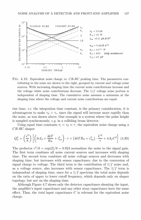
NOISE ANALYSIS OF A DETECTOR AND FRONT-END AMPLIFIER 147
0.01 0.1 1 10
PEAKING TIM E (µs)
101
102
103
104EQUIVALENTNOISECHARGE(e)
CURRENT NO ISEVOLTAGE NO ISE
1/f
R S
ena
Id
R P
ina
Id = 10 nA
R P = 10 M
ina = 0.2 pA/H z1/2
ena = 5 nA/H z1/2
Af = 10-11 V2
R S = 400 (strip resistance)
Cd = 10 pF
Fig. 4.10. Equivalent noise charge vs. CR-RC peaking time. The parameters con-
tributing to the noise are shown to the right, grouped by current and voltage noise
sources. With increasing shaping time the current noise contributions increase and
the voltage white noise contributions decrease. The 1/f voltage noise portion is
independent of shaping time. The cumulative noise assumes a minimum at the
shaping time where the voltage and current noise contributions are equal.
rise time, i.e. the integration time constant, is the primary consideration, it isadvantageous to make τd > τi, since the signal will increase more rapidly thanthe noise, as was shown above. One example is a system where the pulse heightis sampled synchronously, e.g. in a colliding beam detector.
Using equal time constants τi = τd ≡ τ , the equivalent noise charge using aCR-RC shaper
Q2n =
(
ǫ2
8
)[(
2eId +4kT
RP+ i2na
)
· τ +(
4kTRS + e2na
)
· C2
τ+ 4AfC2
]
(4.20)
The prefactor ǫ2/8 = exp(2)/8 = 0.924 normalizes the noise to the signal gain.The first term combines all noise current sources and increases with shapingtime. The second term combines all noise voltage sources and decreases withshaping time, but increases with sensor capacitance, due to the conversion ofsignal charge to voltage. The third term is the contribution of 1/f noise and,as a voltage source, also increases with sensor capacitance. The 1/f term isindependent of shaping time, since for a 1/f spectrum the total noise dependson the ratio of upper to lower cutoff frequency, which depends only on shapertopology, but not on the shaping time.
Although Figure 4.7 shows only the detector capacitance shunting the input,the amplifier’s input capacitance and any other stray capacitance have the sameeffect. Thus, the total input capacitance C is relevant for the equivalent noisecharge.
148 SIGNAL PROCESSING
Figure 4.10 shows a typical plot of equivalent noise charge vs. peaking time,with representative contributions from the individual noise sources. At shortpeaking times the voltage noise dominates, whereas at long peaking times thecurrent noise takes over. Qn assumes a minimum when the current and voltagenoise contributions are equal. Increasing the voltage contribution, e.g. by in-creasing the sensor capacitance, shifts the voltage noise asymptote upwards andthe optimum peaking time to longer values. Conversely, increased current noiseshifts the optimum to smaller peaking times. The presence of 1/f noise flattensthe minimum. The next section shows examples to illustrate this.
The contribution of noise current vs. shaping time is intuitive when viewed inthe time domain. Since every shaper also acts as an integrator, one can view thetotal shot noise as the result of “counting electrons”. Assume an ideal integratorthat records all charge uniformly within a time T . The number of electron chargesmeasured is Ne = IdT/e. The associated noise is the fluctuation in the numberof electron charges recorded σn =
√Ne ∝
√T .
Does this also apply to an AC-coupled system, where no DC component flows,so the integrated net charge is zero? Since shot noise is a fluctuation, the currentundergoes both positive and negative excursions. Although the DC componentis not passed through an AC coupled system, the excursions are. Since, on theaverage, each fluctuation requires a positive and a negative zero crossing, theprocess of “counting electrons” is actually the counting of zero crossings, whichin a detailed analysis yields the same result.
For quick estimates one can use the following formula, which assumes an FETamplifier (negligible ina).
Q2n = 12
[
e2
nA · ns
]
Idτ + 6 · 105
[
e2kΩ
ns
]
τ
Rp+ 3.6 · 104
[
e2ns
(pF)2(nV)
2/Hz
]
e2n
C2
τ.
(4.21)Here the equivalent noise charge is expressed in electrons. To convert to energy,Qn = 1 e corresponds to 3.6 eV in Si and 2.9 eV in Ge.
4.4 Examples
4.4.1 Photodiode readout
The system described in this example was designed for medical imaging (positronemission tomography – PET). Images are formed by introducing a positron-emitting tracer into the body and recording the collinearly emitted annihilationgamma rays. The system utilizes both the direction of the emitted gamma andthe time-of-flight (Choong et al. 2002). A detector module is shown in Figure4.11. To obtain high efficiency for the 511keV gamma radiation originating fromelectron-positron annihilation, the primary sensor is a scintillator coupled to aphotomultiplier tube. To obtain the desired position resolution the cross sectionof each scintillator is about 3×3 mm2. The photomultiplier is used to provide thetiming information. To reduce costs, an array of 64 BGO crystals is coupled toa one inch square photomultiplier tube with a single anode. An array of silicon
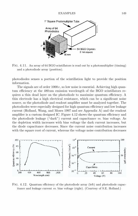
EXAMPLES 149
Fig. 4.11. An array of 64 BGO scintillators is read out by a photomultiplier (timimg)
and a photodiode array (position).
photodiodes senses a portion of the scintillation light to provide the positioninformation.
The signals are of order 1000 e, so low noise is essential. Achieving high quan-tum efficiency at the 480nm emission wavelength of the BGO scintillators re-quires a thin dead layer on the photodiode to maximize quantum efficiency. Athin electrode has a high electrical resistance, which can be a significant noisesource, so the photodiode and readout amplifier must be analyzed together. Thephotodiodes were especially designed for high quantum efficiency and low leakagecurrent (Holland, Wang, and Moses 1997 and see Appendix A) and the readoutamplifier is a custom designed IC. Figure 4.12 shows the quantum efficiency andthe photodiode leakage (“dark”) current and capacitance vs. bias voltage. Asthe depletion width increases with bias voltage the dark current increases, butthe diode capacitance decreases. Since the current noise contribution increaseswith the square root of current, whereas the voltage noise contribution decreases
Fig. 4.12. Quantum efficiency of the photodiode array (left) and photodiode capac-
itance and leakage current vs. bias voltage (right). (Courtesy of S.E. Holland.)
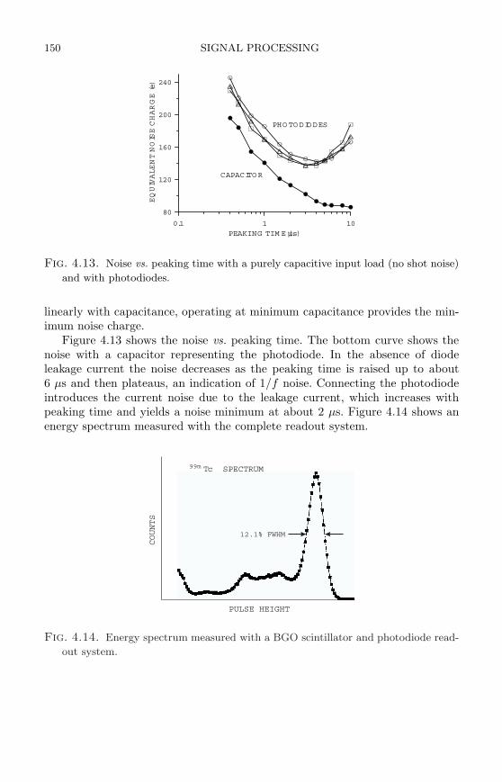
150 SIGNAL PROCESSING
0.1 1 10
PEAKING TIM E (µs)
80
120
160
200
240
EQUIVALENTNOISECHARGE(e)
CAPACITOR
PHOTODIODES
Fig. 4.13. Noise vs. peaking time with a purely capacitive input load (no shot noise)
and with photodiodes.
linearly with capacitance, operating at minimum capacitance provides the min-imum noise charge.
Figure 4.13 shows the noise vs. peaking time. The bottom curve shows thenoise with a capacitor representing the photodiode. In the absence of diodeleakage current the noise decreases as the peaking time is raised up to about6 µs and then plateaus, an indication of 1/f noise. Connecting the photodiodeintroduces the current noise due to the leakage current, which increases withpeaking time and yields a noise minimum at about 2 µs. Figure 4.14 shows anenergy spectrum measured with the complete readout system.
Tc SPECTRUM99m
PULSE HEIGHT
COUNTS
12.1% FWHM
Fig. 4.14. Energy spectrum measured with a BGO scintillator and photodiode read-
out system.
EXAMPLES 151
4.4.2 High-rate x-ray spectroscopy
This example uses a silicon strip detector, but not in its usual role of providingposition sensing, but in an x-ray spectroscopy system that achieves high ratesby distributing the total rate over many parallel readout channels (Ludewigtet al. 1994). For example, a single readout channel with a shaping time of 1µslimits the pulse rate to about 104 s−1. If a sensor is electrically segmented bysubdividing its electrode into an array of strips or pixels, each electrode willcapture only a fraction of the total rate. Thus, if a sensor electrode is segmentedN -fold, the rate in a single electrode will be only 1/N of the total. This onlyapplies to localized charge deposition, as is the case for gamma and x-rays of< 30 keV in silicon, where the energy deposition is dominated by photoelectricabsorption (Figure 1.20). Apart from reducing the rate per channel, segmentationalso reduces the capacitance per electrode, so one can achieve the same noiselevel at a smaller shaping time, which further increases the rate capability. Thisdetector was designed for use at synchrotron light sources, where the small beamspot allows the use of short strip electrodes of 2mm length. The readout pitch is100µm. Figure 4.15 shows a cross section of the sensor (Ludewigt et al. 1996).
The sensor is read out by a custom-designed monolithic integrated circuitwith 64 parallel readout channels (Krieger, Kipnis, and Ludewigt 1998). Eachreadout channel includes a charge-sensitive amplifier, a CR-RC2 shaper withadjustable shaping time and gain, and an output buffer (Figure 4.16). The shaperoutputs are fed to a bank of parallel analog-to-digital converters.
Figure 4.17 shows initial results of the noise vs. peaking time. Data are shownfor the electronics with an open input and with purely capacitive loads of 0.38 and0.75 pF. Here the lower three curves show the noise decreasing with increasingpeaking time, but leveling off above 2 or 4µs. The lower capacitance yields lowernoise, as expected for the voltage noise contribution. At small peaking timesthe noise is dominated by the white voltage noise component, so it decreases
Fig. 4.15. Cross-section of the silicon strip sensor used for high-rate x-ray spec-
troscopy.
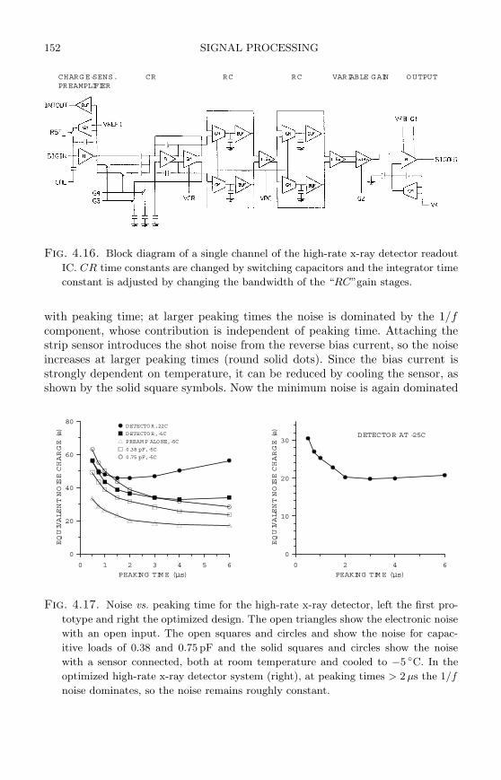
152 SIGNAL PROCESSING
CHARGE-SENS. CR RC RC VARIABLE GAIN OUTPUT PREAMPLIFIER
Fig. 4.16. Block diagram of a single channel of the high-rate x-ray detector readout
IC. CR time constants are changed by switching capacitors and the integrator time
constant is adjusted by changing the bandwidth of the “RC”gain stages.
with peaking time; at larger peaking times the noise is dominated by the 1/fcomponent, whose contribution is independent of peaking time. Attaching thestrip sensor introduces the shot noise from the reverse bias current, so the noiseincreases at larger peaking times (round solid dots). Since the bias current isstrongly dependent on temperature, it can be reduced by cooling the sensor, asshown by the solid square symbols. Now the minimum noise is again dominated
0 1 2 3 4 5 6
PEAKING TIM E (µs)
0
20
40
60
80
EQUIVALENTNOISECHARGE(e)
DETECTO R, 22C
DETECTO R, -5C
PREAM P ALO NE, -5C
0.38 pF, -5C
0.75 pF, -5C
0 2 4 6
PEAKING TIM E (µs)
0
10
20
30
EQUIVALENTNOISECHARGE(e)
DETECTOR AT -25C
Fig. 4.17. Noise vs. peaking time for the high-rate x-ray detector, left the first pro-
totype and right the optimized design. The open triangles show the electronic noise
with an open input. The open squares and circles and show the noise for capac-
itive loads of 0.38 and 0.75 pF and the solid squares and circles show the noise
with a sensor connected, both at room temperature and cooled to −5 C. In the
optimized high-rate x-ray detector system (right), at peaking times > 2 µs the 1/f
noise dominates, so the noise remains roughly constant.
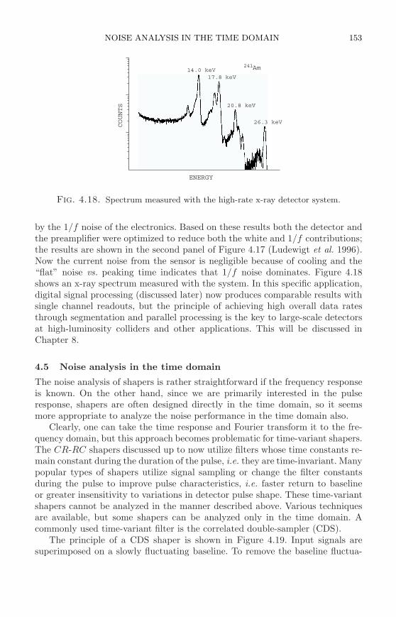
NOISE ANALYSIS IN THE TIME DOMAIN 153
14.0 keV17.8 keV
20.8 keV
26.3 keV
Am241
ENERGY
COUNTS
Fig. 4.18. Spectrum measured with the high-rate x-ray detector system.
by the 1/f noise of the electronics. Based on these results both the detector andthe preamplifier were optimized to reduce both the white and 1/f contributions;the results are shown in the second panel of Figure 4.17 (Ludewigt et al. 1996).Now the current noise from the sensor is negligible because of cooling and the“flat” noise vs. peaking time indicates that 1/f noise dominates. Figure 4.18shows an x-ray spectrum measured with the system. In this specific application,digital signal processing (discussed later) now produces comparable results withsingle channel readouts, but the principle of achieving high overall data ratesthrough segmentation and parallel processing is the key to large-scale detectorsat high-luminosity colliders and other applications. This will be discussed inChapter 8.
4.5 Noise analysis in the time domain
The noise analysis of shapers is rather straightforward if the frequency responseis known. On the other hand, since we are primarily interested in the pulseresponse, shapers are often designed directly in the time domain, so it seemsmore appropriate to analyze the noise performance in the time domain also.
Clearly, one can take the time response and Fourier transform it to the fre-quency domain, but this approach becomes problematic for time-variant shapers.The CR-RC shapers discussed up to now utilize filters whose time constants re-main constant during the duration of the pulse, i.e. they are time-invariant. Manypopular types of shapers utilize signal sampling or change the filter constantsduring the pulse to improve pulse characteristics, i.e. faster return to baselineor greater insensitivity to variations in detector pulse shape. These time-variantshapers cannot be analyzed in the manner described above. Various techniquesare available, but some shapers can be analyzed only in the time domain. Acommonly used time-variant filter is the correlated double-sampler (CDS).
The principle of a CDS shaper is shown in Figure 4.19. Input signals aresuperimposed on a slowly fluctuating baseline. To remove the baseline fluctua-
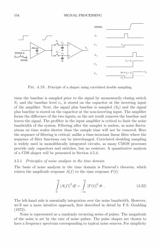
154 SIGNAL PROCESSING
SIGNALS
NOISE
S
S
S
S
VV
V
V
V
Vo
SIGNAL
v
v
v
v v
v
v
n
n
s
s s
n
n
+
+v=
1
1
2
2
11
2
o
2
Fig. 4.19. Principle of a shaper using correlated double sampling.
tions the baseline is sampled prior to the signal by momentarily closing switchS1 and the baseline level vn is stored on the capacitor at the inverting inputof the amplifier. Next, the signal plus baseline is sampled (S2) and the signalplus baseline is stored on the capacitor at the non-inverting input. The amplifierforms the difference of the two inputs, so the net result removes the baseline andleaves the signal. The prefilter in the input amplifier is critical to limit the noisebandwidth of the system. Filtering after the sampler is useless, as noise fluctu-ations on time scales shorter than the sample time will not be removed. Herethe sequence of filtering is critical, unlike a time-invariant linear filter where thesequence of filter functions can be interchanged. Correlated doubling samplingis widely used in monolithically integrated circuits, as many CMOS processesprovide only capacitors and switches, but no resistors. A quantitative analysisof a CDS shaper will be presented in Section 4.5.4.
4.5.1 Principles of noise analysis in the time domain
The basis of noise analysis in the time domain is Parseval’s theorem, whichrelates the amplitude response A(f) to the time response F (t):
∞∫
0
|A(f)|2 df =
∞∫
−∞
[F (t)]2dt . (4.22)
The left-hand side is essentially integration over the noise bandwidth. However,we’ll use a more intuitive approach, first described in detail by F.S. Goulding(1972).
Noise is represented as a randomly recurring series of pulses. The magnitudeof the noise is set by the rate of noise pulses. The pulse shapes are chosen tohave a frequency spectrum corresponding to typical noise sources. For simplicity
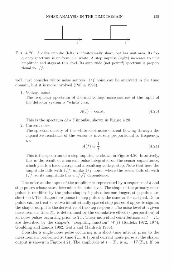
NOISE ANALYSIS IN THE TIME DOMAIN 155
tt
Fig. 4.20. A delta impulse (left) is infinitesimally short, but has unit area. Its fre-
quency spectrum is uniform, i.e. white. A step impulse (right) increases to unit
amplitude and stays at this level. Its amplitude (not power!) spectrum is propor-
tional to 1/f .
we’ll just consider white noise sources. 1/f noise can be analyzed in the timedomain, but it is more involved (Pullia 1998).
1. Voltage noiseThe frequency spectrum of thermal voltage noise sources at the input ofthe detector system is “white”, i.e.
A(f) = const. (4.23)
This is the spectrum of a δ impulse, shown in Figure 4.20.
2. Current noiseThe spectral density of the white shot noise current flowing through thecapacitive reactance of the sensor is inversely proportional to frequency,i.e.
A(f) ∝ 1
f. (4.24)
This is the spectrum of a step impulse, as shown in Figure 4.20. Intuitively,this is the result of a current pulse integrated on the sensor capacitance,which yields a fixed charge and a resulting voltage step. Note that here theamplitude falls with 1/f , unlike 1/f noise, where the power falls off with1/f , so its amplitude has a 1/
√f dependence.
The noise at the input of the amplifier is represented by a sequence of δ andstep pulses whose rates determine the noise level. The shape of the primary noisepulses is modified by the pulse shaper; δ pulses become longer, step pulses areshortened. The shaper’s response to step pulses is the same as for a signal. Deltapulses can be treated as two infinitesimally spaced step pulses of opposite sign, sothe shaper output is the derivative of the step response. The noise level at a givenmeasurement time Tm is determined by the cumulative effect (superposition) ofall noise pulses occurring prior to Tm. Their individual contributions at t = Tm
are described by the shaper’s “weighting function” W (t) (Radeka 1972, 1974,Goulding and Landis 1982, Gatti and Manfredi 1986).
Consider a single noise pulse occurring in a short time interval prior to themeasurement performed at time Tm. A typical current noise pulse at the shaperoutput is shown in Figure 4.21. The amplitude at t = Tm is an = W (Tm). If, on
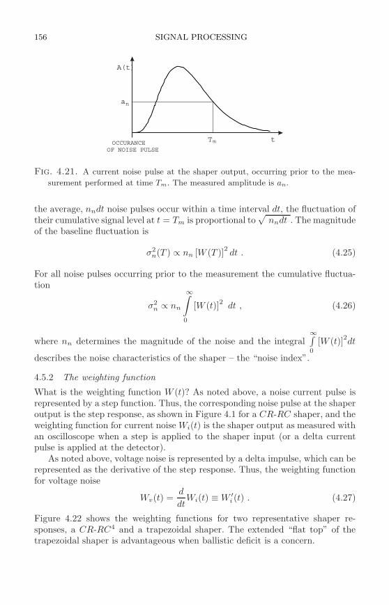
156 SIGNAL PROCESSING
A(t)
OCCURANCEOF NOISE PULSE
T t
a
m
n
Fig. 4.21. A current noise pulse at the shaper output, occurring prior to the mea-
surement performed at time Tm. The measured amplitude is an.
the average, nndt noise pulses occur within a time interval dt, the fluctuation oftheir cumulative signal level at t = Tm is proportional to
√nndt . The magnitude
of the baseline fluctuation is
σ2n(T ) ∝ nn [W (T )]
2dt . (4.25)
For all noise pulses occurring prior to the measurement the cumulative fluctua-tion
σ2n ∝ nn
∞∫
0
[W (t)]2 dt , (4.26)
where nn determines the magnitude of the noise and the integral∞∫
0
[W (t)]2dt
describes the noise characteristics of the shaper – the “noise index”.
4.5.2 The weighting function
What is the weighting function W (t)? As noted above, a noise current pulse isrepresented by a step function. Thus, the corresponding noise pulse at the shaperoutput is the step response, as shown in Figure 4.1 for a CR-RC shaper, and theweighting function for current noise Wi(t) is the shaper output as measured withan oscilloscope when a step is applied to the shaper input (or a delta currentpulse is applied at the detector).
As noted above, voltage noise is represented by a delta impulse, which can berepresented as the derivative of the step response. Thus, the weighting functionfor voltage noise
Wv(t) =d
dtWi(t) ≡ W ′
i (t) . (4.27)
Figure 4.22 shows the weighting functions for two representative shaper re-sponses, a CR-RC4 and a trapezoidal shaper. The extended “flat top” of thetrapezoidal shaper is advantageous when ballistic deficit is a concern.
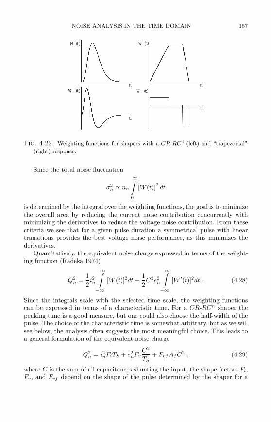
NOISE ANALYSIS IN THE TIME DOMAIN 157
t
W (t) W (t)
t
t
W'(t) W '(t)
t
Fig. 4.22. Weighting functions for shapers with a CR-RC4 (left) and “trapezoidal”
(right) response.
Since the total noise fluctuation
σ2n ∝ nn
∞∫
0
[W (t)]2dt
is determined by the integral over the weighting functions, the goal is to minimizethe overall area by reducing the current noise contribution concurrently withminimizing the derivatives to reduce the voltage noise contribution. From thesecriteria we see that for a given pulse duration a symmetrical pulse with lineartransitions provides the best voltage noise performance, as this minimizes thederivatives.
Quantitatively, the equivalent noise charge expressed in terms of the weight-ing function (Radeka 1974)
Q2n =
1
2i2n
∞∫
−∞
[W (t)]2dt +1
2C2e2
n
∞∫
−∞
[W ′(t)]2dt . (4.28)
Since the integrals scale with the selected time scale, the weighting functionscan be expressed in terms of a characteristic time. For a CR-RCn shaper thepeaking time is a good measure, but one could also choose the half-width of thepulse. The choice of the characteristic time is somewhat arbitrary, but as we willsee below, the analysis often suggests the most meaningful choice. This leads toa general formulation of the equivalent noise charge
Q2n = i2nFiTS + e2
nFvC2
TS+ Fvf AfC2 , (4.29)
where C is the sum of all capacitances shunting the input, the shape factors Fi,Fv , and Fvf depend on the shape of the pulse determined by the shaper for a
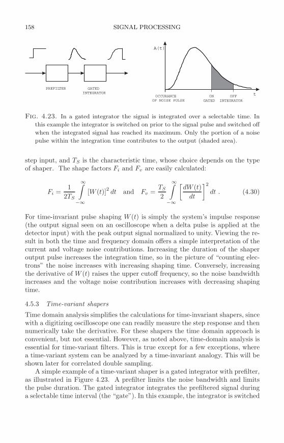
158 SIGNAL PROCESSING
PREFILTER GATEDINTEGRATOR t
A(t)
ON OFFOCCURANCEOF NOISE PULSE GATED INTEGRATOR
Fig. 4.23. In a gated integrator the signal is integrated over a selectable time. In
this example the integrator is switched on prior to the signal pulse and switched off
when the integrated signal has reached its maximum. Only the portion of a noise
pulse within the integration time contributes to the output (shaded area).
step input, and TS is the characteristic time, whose choice depends on the typeof shaper. The shape factors Fi and Fv are easily calculated:
Fi =1
2TS
∞∫
−∞
[W (t)]2 dt and Fv =TS
2
∞∫
−∞
[
dW (t)
dt
]2
dt . (4.30)
For time-invariant pulse shaping W (t) is simply the system’s impulse response(the output signal seen on an oscilloscope when a delta pulse is applied at thedetector input) with the peak output signal normalized to unity. Viewing the re-sult in both the time and frequency domain offers a simple interpretation of thecurrent and voltage noise contributions. Increasing the duration of the shaperoutput pulse increases the integration time, so in the picture of “counting elec-trons” the noise increases with increasing shaping time. Conversely, increasingthe derivative of W (t) raises the upper cutoff frequency, so the noise bandwidthincreases and the voltage noise contribution increases with decreasing shapingtime.
4.5.3 Time-variant shapers
Time domain analysis simplifies the calculations for time-invariant shapers, sincewith a digitizing oscilloscope one can readily measure the step response and thennumerically take the derivative. For these shapers the time domain approach isconvenient, but not essential. However, as noted above, time-domain analysis isessential for time-variant filters. This is true except for a few exceptions, wherea time-variant system can be analyzed by a time-invariant analogy. This will beshown later for correlated double sampling.
A simple example of a time-variant shaper is a gated integrator with prefilter,as illustrated in Figure 4.23. A prefilter limits the noise bandwidth and limitsthe pulse duration. The gated integrator integrates the prefiltered signal duringa selectable time interval (the “gate”). In this example, the integrator is switched
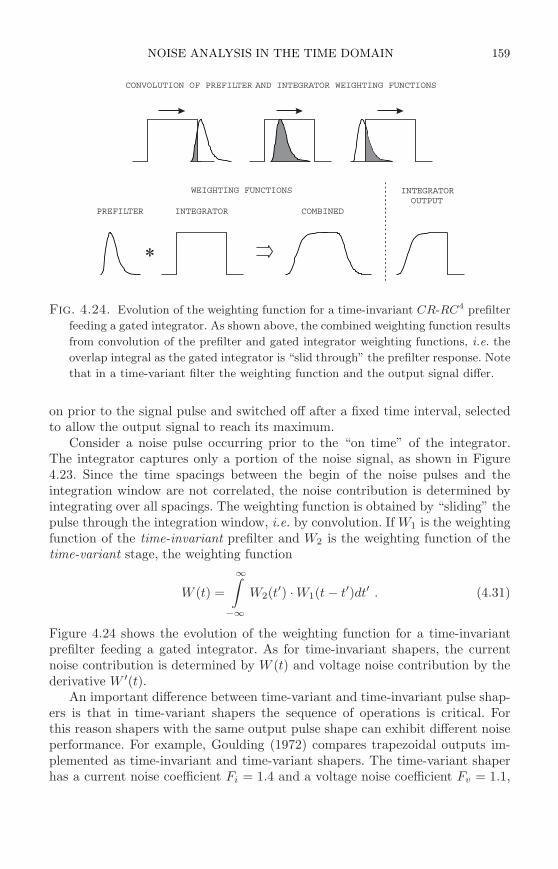
NOISE ANALYSIS IN THE TIME DOMAIN 159
PREFILTER INTEGRATOR
INTEGRATOROUTPUT
COMBINED
CONVOLUTION OF PREFILTER AND INTEGRATOR WEIGHTING FUNCTIONS
WEIGHTING FUNCTIONS
Fig. 4.24. Evolution of the weighting function for a time-invariant CR-RC4 prefilter
feeding a gated integrator. As shown above, the combined weighting function results
from convolution of the prefilter and gated integrator weighting functions, i.e. the
overlap integral as the gated integrator is “slid through” the prefilter response. Note
that in a time-variant filter the weighting function and the output signal differ.
on prior to the signal pulse and switched off after a fixed time interval, selectedto allow the output signal to reach its maximum.
Consider a noise pulse occurring prior to the “on time” of the integrator.The integrator captures only a portion of the noise signal, as shown in Figure4.23. Since the time spacings between the begin of the noise pulses and theintegration window are not correlated, the noise contribution is determined byintegrating over all spacings. The weighting function is obtained by “sliding” thepulse through the integration window, i.e. by convolution. If W1 is the weightingfunction of the time-invariant prefilter and W2 is the weighting function of thetime-variant stage, the weighting function
W (t) =
∞∫
−∞
W2(t′) · W1(t − t′)dt′ . (4.31)
Figure 4.24 shows the evolution of the weighting function for a time-invariantprefilter feeding a gated integrator. As for time-invariant shapers, the currentnoise contribution is determined by W (t) and voltage noise contribution by thederivative W ′(t).
An important difference between time-variant and time-invariant pulse shap-ers is that in time-variant shapers the sequence of operations is critical. Forthis reason shapers with the same output pulse shape can exhibit different noiseperformance. For example, Goulding (1972) compares trapezoidal outputs im-plemented as time-invariant and time-variant shapers. The time-variant shaperhas a current noise coefficient Fi = 1.4 and a voltage noise coefficient Fv = 1.1,
160 SIGNAL PROCESSING
whereas the time-invariant shaper has Fi = 0.8 and Fv = 2.2. The time-varianttrapezoid has more current noise and less voltage noise than the time-invariantversion.
4.5.4 Noise analysis of a correlated-double sample pulse shaper
Correlated double sampling was already explained above. Now we apply time-domain noise analysis to this shaper, which is widely used in monolithic inte-grated circuit readouts. Referring to Figure 4.19, the signal is first sent througha prefilter, which is a simple RC low-pass filter with a time constant τ . Its stepresponse is 1 − exp(−t/τ), where the peak amplitude is normalized to one. Theweighting function is the convolution of the RC prefilter response with the twosequential samples of opposite sign. We assume that the amplitude is sampledduring a time that is small compared to the time interval between samples T , sothe sample pulse can be represented as a δ function. Thus, the weighting functionis
t < 0 : W (t) = 0
0 ≤ t ≤ T : W (t) = 1− e−t/τ
t > T : W (t) =(
1 − e−t/τ)
−(
1 − e−(t−T )/τ)
= e−t/τ(
eT/τ − 1)
.
4.5.4.1 Current noise The current (shot) noise contribution
Q2ni =
1
2i2n
∞∫
−∞
[W (t)]2dt . (4.32)
The current noise index
Ni =
∞∫
−∞
[W (t)]2dt
Ni =
T∫
0
(
1 − e−t/τ)2
dt +
∞∫
T
e−2t/τ(
eT/τ − 1)2
dt
Ni = T + τe−T/τ − τ = T + τ(
e−T/τ − 1)
. (4.33)
Increasing the sampling time T increases the noise, but since the expressionin brackets is always negative, the effective integration time is less than T . Toobtain the equivalent noise charge the noise must be normalized to the signal.The signal amplitude at the output of the prefilter at the time of the secondsample
Vs/Vi = 1 − e−T/τ , (4.34)
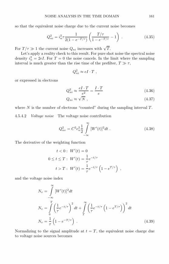
NOISE ANALYSIS IN THE TIME DOMAIN 161
so that the equivalent noise charge due to the current noise becomes
Q2ni = i2nτ
1
2(1 − e−T/τ )
(
T/τ
1 − e−T/τ− 1
)
. (4.35)
For T/τ ≫ 1 the current noise Qni increases with√
T .Let’s apply a reality check to this result. For pure shot noise the spectral noise
density i2n = 2eI . For T = 0 the noise cancels. In the limit where the samplinginterval is much greater than the rise time of the prefilter, T ≫ τ ,
Q2ni ≈ eI · T ,
or expressed in electrons
Q2ni ≈
eI · Te2
=I · T
e(4.36)
Qni ≈√
N , (4.37)
where N is the number of electrons “counted” during the sampling interval T .
4.5.4.2 Voltage noise The voltage noise contribution
Q2nv = C2e2
n
1
2
∞∫
−∞
[W ′(t)]2dt . (4.38)
The derivative of the weighting function
t < 0 : W ′(t) = 0
0 ≤ t ≤ T : W ′(t) =1
τe−t/τ
t > T : W ′(t) =1
τe−t/τ
(
1 − eT/τ)
,
and the voltage noise index
Nv =
∞∫
−∞
[W ′(t)]2dt
Nv =
T∫
0
(
1
τe−t/τ
)2
dt +
∞∫
T
(
1
τe−t/τ
(
1 − eT/τ)
)2
dt
Nv =1
τ
(
1 − e−T/τ)
. (4.39)
Normalizing to the signal amplitude at t = T , the equivalent noise charge dueto voltage noise sources becomes
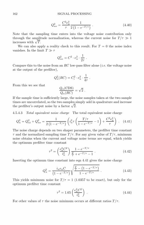
162 SIGNAL PROCESSING
Q2nv =
C2e2n
τ
1
2(
1 − e−T/τ) . (4.40)
Note that the sampling time enters into the voltage noise contribution onlythrough the amplitude normalization, whereas the current noise for T/τ ≫ 1increases with
√T .
We can also apply a reality check to this result. For T = 0 the noise indexvanishes. In the limit T ≫ τ
Q2nv = C2 · e2
n · 1
2τ.
Compare this to the noise from an RC low-pass filter alone (i.e. the voltage noiseat the output of the prefilter),
Q2n(RC) = C2
i · e2n · 1
4τ.
From this we see thatQn(CDS)
Qn(RC)=
√2 .
If the sample time is sufficiently large, the noise samples taken at the two sampletimes are uncorrelated, so the two samples simply add in quadrature and increasethe prefilter’s output noise by a factor
√2.
4.5.4.3 Total equivalent noise charge The total equivalent noise charge
Q2n = Q2
ni + Q2nv =
1
2(
1 − e−T/τ)
(
i2nτ
(
T/τ
1 − e−T/τ− 1
)
+C2e2
n
τ
)
. (4.41)
The noise charge depends on two shaper parameters, the prefilter time constantτ and the normalized sampling time T/τ . For any given value of T/τ , minimumnoise obtains when the current and voltage noise terms are equal, which yieldsthe optimum prefilter time constant
τ2 =
(
e2nC2
i2n
)
1 − e−T/τ
Tτ + e−T/τ − 1
. (4.42)
Inserting the optimum time constant into eqn 4.41 gives the noise charge
Q2n =
inenC(
1 − e−T/τ)
√
Tτ −
(
1 − e−T/τ)
1 − e−T/τ. (4.43)
This yields minimum noise for T/τ = 1 (1.0357 to be exact), but only for theoptimum prefilter time constant
τ2 = 1.65
(
e2nC2
i2n
)
. (4.44)
For other values of τ the noise minimum occurs at different ratios T/τ .
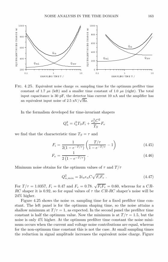
NOISE ANALYSIS IN THE TIME DOMAIN 163
0.1 1 10
SAM PLING TIM E T /
200
400
600
800
1000
EQUIVALENTNOISECHARGE(e)
QnvQni
Qn
0.1 1 10
SAM PLING TIM E T /
0
200
400
600
800
1000
EQUIVALENTNOISECHARGE(e)
Qni Qnv
Qn
Fig. 4.25. Equivalent noise charge vs. sampling time for the optimum prefilter time
constant of 1.7 µs (left) and a smaller time constant of 1.0 µs (right). The total
input capacitance is 30 pF, the detector bias current 10 nA and the amplifier has
an equivalent input noise of 2.5 nV/√
Hz.
In the formalism developed for time-invariant shapers
Q2n = i2nTSFi +
e2nC2
TSFv
we find that the characteristic time TS = τ and
Fi =1
2(1 − e−T/τ )
(
T/τ
1 − e−T/τ− 1
)
(4.45)
Fv =1
2(
1 − e−T/τ) . (4.46)
Minimum noise obtains for the optimum values of τ and T/τ
Q2n,min = 2inenC
√
FiFv . (4.47)
For T/τ = 1.0357, Fi = 0.47 and Fv = 0.78.√
FiFv = 0.60, whereas for a CR-RC shaper it is 0.92, so for equal values of τ the CR-RC shaper’s noise will be24% higher.
Figure 4.25 shows the noise vs. sampling time for a fixed prefilter time con-stant. The left panel is for the optimum shaping time, so the noise attains ashallow minimum at T/τ = 1, as expected. In the second panel the prefilter timeconstant is half the optimum value. Now the minimum is at T/τ = 1.5, but thenoise is only 4% higher. At the optimum prefilter time constant the noise mini-mum occurs when the current and voltage noise contributions are equal, whereasfor the non-optimum time constant this is not the case. At small sampling timesthe reduction in signal amplitude increases the equivalent noise charge. Figure
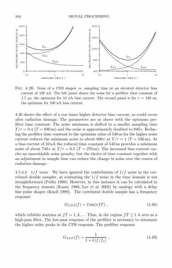
164 SIGNAL PROCESSING
0.1 1 10
SAM PLING TIM E T /
0
400
800
1200
1600
2000
EQUIVALENTNOISECHARGE(e)
Qni
Qnv
Qn
0.1 1 10
SAM PLING TIM E T /
400
800
1200
1600
2000
EQUIVALENTNOISECHARGE(e)
Qni Qnv
Qn
Fig. 4.26. Noise of a CDS shaper vs. sampling time at an elevated detector bias
current of 100 nA. The left panel shows the noise for a prefilter time constant of
1.7 µs, the optimum for 10 nA bias current. The second panel is for τ = 540 ns,
the optimum for 100 nA bias current.
4.26 shows the effect of a ten times higher detector bias current, as could occurafter radiation damage. The parameters are as above with the optimum pre-filter time constant. The noise minimum is shifted to a smaller sampling timeT/τ = 0.4 (T = 680ns) and the noise is approximately doubled to 940 e. Reduc-ing the prefilter time constant to the optimum value of 540ns for the higher noisecurrent reduces the minimum noise to about 800 e at T/τ = 1 (T = 540ns). Ata bias current of 10 nA the reduced time constant of 540ns provides a minimumnoise of about 740 e at T/τ = 0.5 (T = 270ns). The increased bias current car-ries an unavoidable noise penalty, but the choice of time constant together withan adjustment in sample time can reduce the change in noise over the course ofradiation damage.
4.5.4.4 1/f noise We have ignored the contribution of 1/f noise in the cor-related double sampler, as evaluating the 1/f noise in the time domain is notstraightforward (Pullia 1998). However, in this instance it can be calculated inthe frequency domain (Kansy 1980, Lee et al. 2002) by analogy with a delayline pulse shaper (Knoll 1999). The correlated double sample has a frequencyresponse
GCDS(f) = 2 sin(πfT ) , (4.48)
which exhibits maxima at fT = 1, 3, . . . Thus, in the regime fT ≤ 1 it acts as ahigh-pass filter. The low-pass response of the prefilter is necessary to attenuatethe higher order peaks in the CDS response. The prefilter response
GLPF (f) =1
1 + i (f/fu), (4.49)
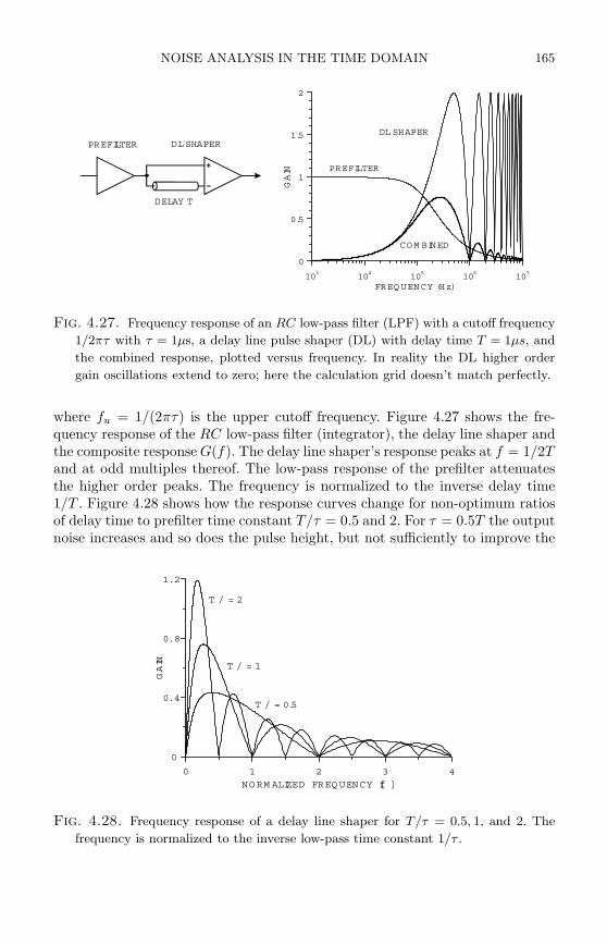
NOISE ANALYSIS IN THE TIME DOMAIN 165
103
104
105
106
107
FREQUENCY (Hz)
0
0.5
1
1.5
2
GAIN PREFILTER
DL SHAPER
COM BINED
DELAY T
PREFILTER DLSHAPER
Fig. 4.27. Frequency response of an RC low-pass filter (LPF) with a cutoff frequency
1/2πτ with τ = 1µs, a delay line pulse shaper (DL) with delay time T = 1µs, and
the combined response, plotted versus frequency. In reality the DL higher order
gain oscillations extend to zero; here the calculation grid doesn’t match perfectly.
where fu = 1/(2πτ) is the upper cutoff frequency. Figure 4.27 shows the fre-quency response of the RC low-pass filter (integrator), the delay line shaper andthe composite response G(f). The delay line shaper’s response peaks at f = 1/2Tand at odd multiples thereof. The low-pass response of the prefilter attenuatesthe higher order peaks. The frequency is normalized to the inverse delay time1/T . Figure 4.28 shows how the response curves change for non-optimum ratiosof delay time to prefilter time constant T/τ = 0.5 and 2. For τ = 0.5T the outputnoise increases and so does the pulse height, but not sufficiently to improve the
0 1 2 3 4
NORM ALIZED FREQUENCY [ f ]
0
0.4
0.8
1.2
GAIN
T / = 2
T / = 1
T / = 0.5
Fig. 4.28. Frequency response of a delay line shaper for T/τ = 0.5, 1, and 2. The
frequency is normalized to the inverse low-pass time constant 1/τ .
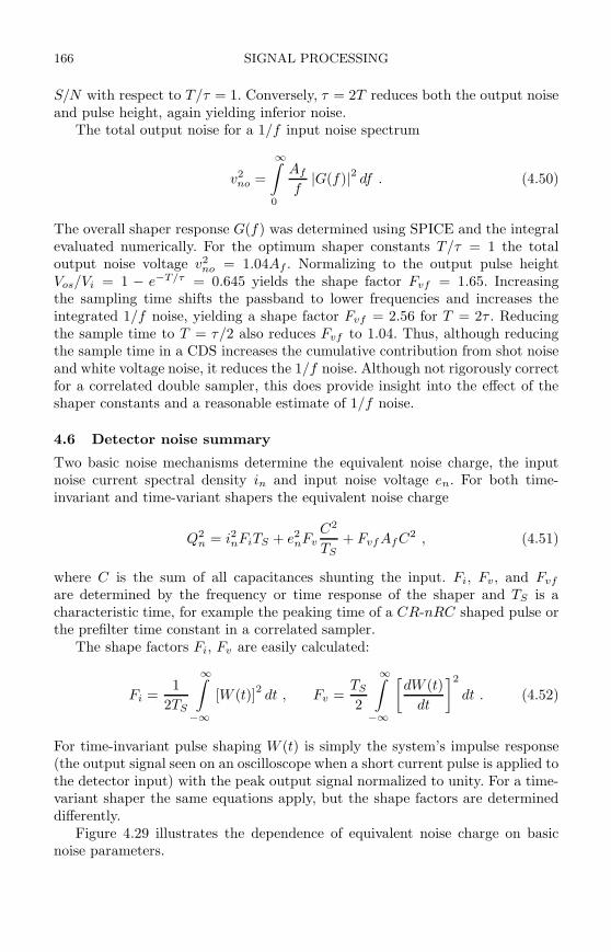
166 SIGNAL PROCESSING
S/N with respect to T/τ = 1. Conversely, τ = 2T reduces both the output noiseand pulse height, again yielding inferior noise.
The total output noise for a 1/f input noise spectrum
v2no =
∞∫
0
Af
f|G(f)|2 df . (4.50)
The overall shaper response G(f) was determined using SPICE and the integralevaluated numerically. For the optimum shaper constants T/τ = 1 the totaloutput noise voltage v2
no = 1.04Af . Normalizing to the output pulse heightVos/Vi = 1 − e−T/τ = 0.645 yields the shape factor Fvf = 1.65. Increasingthe sampling time shifts the passband to lower frequencies and increases theintegrated 1/f noise, yielding a shape factor Fvf = 2.56 for T = 2τ . Reducingthe sample time to T = τ/2 also reduces Fvf to 1.04. Thus, although reducingthe sample time in a CDS increases the cumulative contribution from shot noiseand white voltage noise, it reduces the 1/f noise. Although not rigorously correctfor a correlated double sampler, this does provide insight into the effect of theshaper constants and a reasonable estimate of 1/f noise.
4.6 Detector noise summary
Two basic noise mechanisms determine the equivalent noise charge, the inputnoise current spectral density in and input noise voltage en. For both time-invariant and time-variant shapers the equivalent noise charge
Q2n = i2nFiTS + e2
nFvC2
TS+ Fvf AfC2 , (4.51)
where C is the sum of all capacitances shunting the input. Fi, Fv, and Fvf
are determined by the frequency or time response of the shaper and TS is acharacteristic time, for example the peaking time of a CR-nRC shaped pulse orthe prefilter time constant in a correlated sampler.
The shape factors Fi, Fv are easily calculated:
Fi =1
2TS
∞∫
−∞
[W (t)]2dt , Fv =
TS
2
∞∫
−∞
[
dW (t)
dt
]2
dt . (4.52)
For time-invariant pulse shaping W (t) is simply the system’s impulse response(the output signal seen on an oscilloscope when a short current pulse is applied tothe detector input) with the peak output signal normalized to unity. For a time-variant shaper the same equations apply, but the shape factors are determineddifferently.
Figure 4.29 illustrates the dependence of equivalent noise charge on basicnoise parameters.
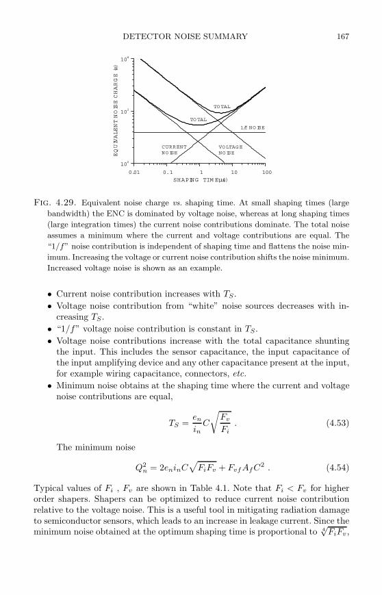
DETECTOR NOISE SUMMARY 167
0.01 0.1 1 10 100
SHAPING TIM E (µs)
102
103
104
EQUIVALENTNOISECHARGE(e)
CURRENTNOISE
VOLTAGENOISE
TO TAL
1/f NOISE
TOTAL
Fig. 4.29. Equivalent noise charge vs. shaping time. At small shaping times (large
bandwidth) the ENC is dominated by voltage noise, whereas at long shaping times
(large integration times) the current noise contributions dominate. The total noise
assumes a minimum where the current and voltage contributions are equal. The
“1/f” noise contribution is independent of shaping time and flattens the noise min-
imum. Increasing the voltage or current noise contribution shifts the noise minimum.
Increased voltage noise is shown as an example.
• Current noise contribution increases with TS .
• Voltage noise contribution from “white” noise sources decreases with in-creasing TS .
• “1/f” voltage noise contribution is constant in TS.
• Voltage noise contributions increase with the total capacitance shuntingthe input. This includes the sensor capacitance, the input capacitance ofthe input amplifying device and any other capacitance present at the input,for example wiring capacitance, connectors, etc.
• Minimum noise obtains at the shaping time where the current and voltagenoise contributions are equal,
TS =en
inC
√
Fv
Fi. (4.53)
The minimum noise
Q2n = 2eninC
√
FiFv + Fvf AfC2 . (4.54)
Typical values of Fi , Fv are shown in Table 4.1. Note that Fi < Fv for higherorder shapers. Shapers can be optimized to reduce current noise contributionrelative to the voltage noise. This is a useful tool in mitigating radiation damageto semiconductor sensors, which leads to an increase in leakage current. Since theminimum noise obtained at the optimum shaping time is proportional to 4
√FiFv ,
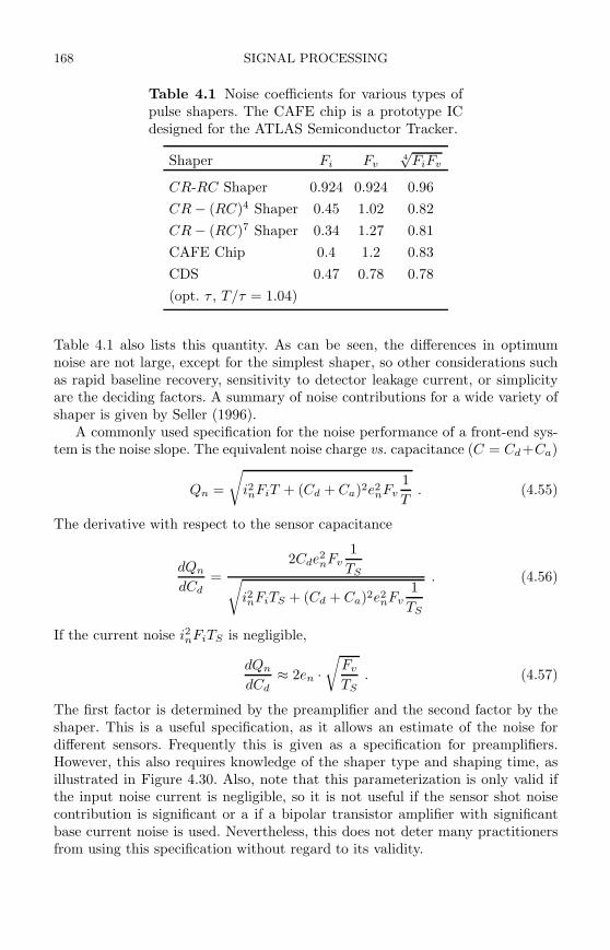
168 SIGNAL PROCESSING
Table 4.1 Noise coefficients for various types ofpulse shapers. The CAFE chip is a prototype ICdesigned for the ATLAS Semiconductor Tracker.
Shaper Fi Fv4√
FiFv
CR-RC Shaper 0.924 0.924 0.96
CR − (RC)4 Shaper 0.45 1.02 0.82
CR − (RC)7 Shaper 0.34 1.27 0.81
CAFE Chip 0.4 1.2 0.83
CDS 0.47 0.78 0.78
(opt. τ , T/τ = 1.04)
Table 4.1 also lists this quantity. As can be seen, the differences in optimumnoise are not large, except for the simplest shaper, so other considerations suchas rapid baseline recovery, sensitivity to detector leakage current, or simplicityare the deciding factors. A summary of noise contributions for a wide variety ofshaper is given by Seller (1996).
A commonly used specification for the noise performance of a front-end sys-tem is the noise slope. The equivalent noise charge vs. capacitance (C = Cd+Ca)
Qn =
√
i2nFiT + (Cd + Ca)2e2nFv
1
T. (4.55)
The derivative with respect to the sensor capacitance
dQn
dCd=
2Cde2nFv
1
TS√
i2nFiTS + (Cd + Ca)2e2nFv
1
TS
. (4.56)
If the current noise i2nFiTS is negligible,
dQn
dCd≈ 2en ·
√
Fv
TS. (4.57)
The first factor is determined by the preamplifier and the second factor by theshaper. This is a useful specification, as it allows an estimate of the noise fordifferent sensors. Frequently this is given as a specification for preamplifiers.However, this also requires knowledge of the shaper type and shaping time, asillustrated in Figure 4.30. Also, note that this parameterization is only valid ifthe input noise current is negligible, so it is not useful if the sensor shot noisecontribution is significant or a if a bipolar transistor amplifier with significantbase current noise is used. Nevertheless, this does not deter many practitionersfrom using this specification without regard to its validity.
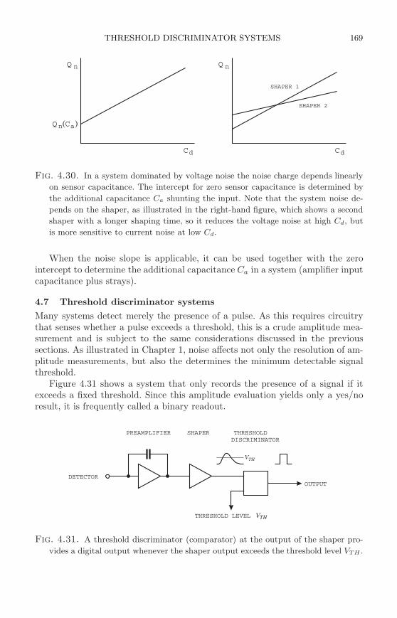
THRESHOLD DISCRIMINATOR SYSTEMS 169
Q
Q Q
C C
n
n n
d d
( )Ca
SHAPER 1
SHAPER 2
Fig. 4.30. In a system dominated by voltage noise the noise charge depends linearly
on sensor capacitance. The intercept for zero sensor capacitance is determined by
the additional capacitance Ca shunting the input. Note that the system noise de-
pends on the shaper, as illustrated in the right-hand figure, which shows a second
shaper with a longer shaping time, so it reduces the voltage noise at high Cd, but
is more sensitive to current noise at low Cd.
When the noise slope is applicable, it can be used together with the zerointercept to determine the additional capacitance Ca in a system (amplifier inputcapacitance plus strays).
4.7 Threshold discriminator systems
Many systems detect merely the presence of a pulse. As this requires circuitrythat senses whether a pulse exceeds a threshold, this is a crude amplitude mea-surement and is subject to the same considerations discussed in the previoussections. As illustrated in Chapter 1, noise affects not only the resolution of am-plitude measurements, but also the determines the minimum detectable signalthreshold.
Figure 4.31 shows a system that only records the presence of a signal if itexceeds a fixed threshold. Since this amplitude evaluation yields only a yes/noresult, it is frequently called a binary readout.
PREAMPLIFIER SHAPER THRESHOLDDISCRIMINATOR
THRESHOLD LEVEL V
DETECTOR
TH
TH
OUTPUT
V
Fig. 4.31. A threshold discriminator (comparator) at the output of the shaper pro-
vides a digital output whenever the shaper output exceeds the threshold level VTH .
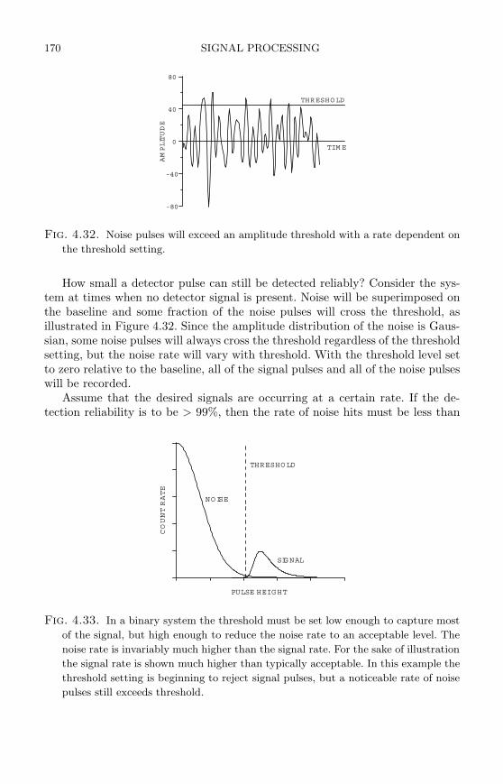
170 SIGNAL PROCESSING
TIM E
-80
-40
0
40
80
AMPLITUDE
THRESHOLD
Fig. 4.32. Noise pulses will exceed an amplitude threshold with a rate dependent on
the threshold setting.
How small a detector pulse can still be detected reliably? Consider the sys-tem at times when no detector signal is present. Noise will be superimposed onthe baseline and some fraction of the noise pulses will cross the threshold, asillustrated in Figure 4.32. Since the amplitude distribution of the noise is Gaus-sian, some noise pulses will always cross the threshold regardless of the thresholdsetting, but the noise rate will vary with threshold. With the threshold level setto zero relative to the baseline, all of the signal pulses and all of the noise pulseswill be recorded.
Assume that the desired signals are occurring at a certain rate. If the de-tection reliability is to be > 99%, then the rate of noise hits must be less than
PULSE HEIGHT
COUNTRATE
THRESHOLD
NOISE
SIGNAL
Fig. 4.33. In a binary system the threshold must be set low enough to capture most
of the signal, but high enough to reduce the noise rate to an acceptable level. The
noise rate is invariably much higher than the signal rate. For the sake of illustration
the signal rate is shown much higher than typically acceptable. In this example the
threshold setting is beginning to reject signal pulses, but a noticeable rate of noise
pulses still exceeds threshold.
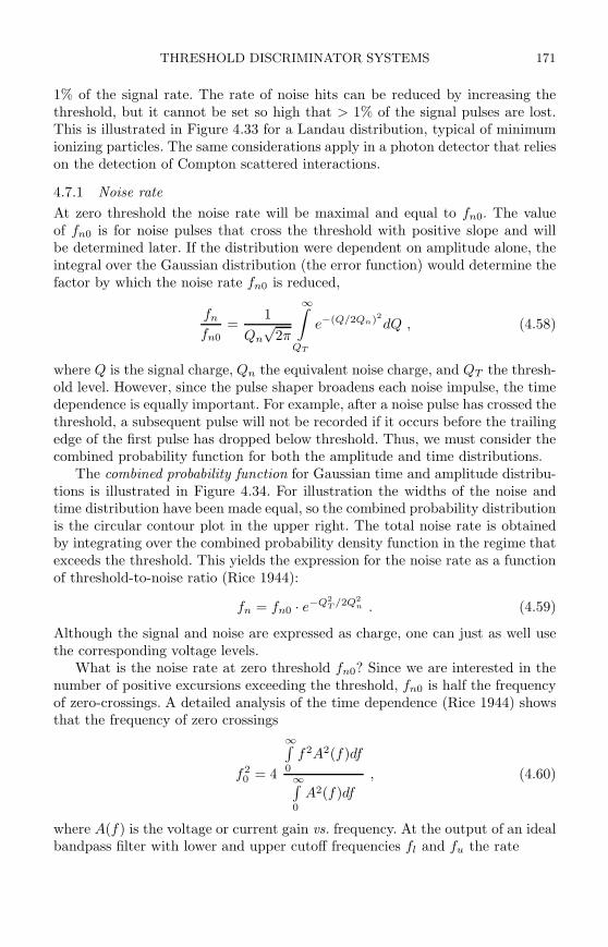
THRESHOLD DISCRIMINATOR SYSTEMS 171
1% of the signal rate. The rate of noise hits can be reduced by increasing thethreshold, but it cannot be set so high that > 1% of the signal pulses are lost.This is illustrated in Figure 4.33 for a Landau distribution, typical of minimumionizing particles. The same considerations apply in a photon detector that relieson the detection of Compton scattered interactions.
4.7.1 Noise rate
At zero threshold the noise rate will be maximal and equal to fn0. The valueof fn0 is for noise pulses that cross the threshold with positive slope and willbe determined later. If the distribution were dependent on amplitude alone, theintegral over the Gaussian distribution (the error function) would determine thefactor by which the noise rate fn0 is reduced,
fn
fn0=
1
Qn
√2π
∞∫
QT
e−(Q/2Qn)2dQ , (4.58)
where Q is the signal charge, Qn the equivalent noise charge, and QT the thresh-old level. However, since the pulse shaper broadens each noise impulse, the timedependence is equally important. For example, after a noise pulse has crossed thethreshold, a subsequent pulse will not be recorded if it occurs before the trailingedge of the first pulse has dropped below threshold. Thus, we must consider thecombined probability function for both the amplitude and time distributions.
The combined probability function for Gaussian time and amplitude distribu-tions is illustrated in Figure 4.34. For illustration the widths of the noise andtime distribution have been made equal, so the combined probability distributionis the circular contour plot in the upper right. The total noise rate is obtainedby integrating over the combined probability density function in the regime thatexceeds the threshold. This yields the expression for the noise rate as a functionof threshold-to-noise ratio (Rice 1944):
fn = fn0 · e−Q2
T /2Q2
n . (4.59)
Although the signal and noise are expressed as charge, one can just as well usethe corresponding voltage levels.
What is the noise rate at zero threshold fn0? Since we are interested in thenumber of positive excursions exceeding the threshold, fn0 is half the frequencyof zero-crossings. A detailed analysis of the time dependence (Rice 1944) showsthat the frequency of zero crossings
f20 = 4
∞∫
0
f2A2(f)df
∞∫
0
A2(f)df
, (4.60)
where A(f) is the voltage or current gain vs. frequency. At the output of an idealbandpass filter with lower and upper cutoff frequencies fl and fu the rate
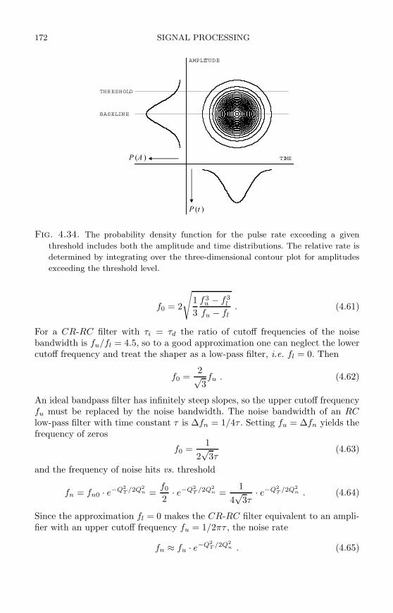
172 SIGNAL PROCESSING
TIME
AMPLITUDE
THRESHOLD
P (A )
P (t )
BASELINE
Fig. 4.34. The probability density function for the pulse rate exceeding a given
threshold includes both the amplitude and time distributions. The relative rate is
determined by integrating over the three-dimensional contour plot for amplitudes
exceeding the threshold level.
f0 = 2
√
1
3
f3u − f3
l
fu − fl. (4.61)
For a CR-RC filter with τi = τd the ratio of cutoff frequencies of the noisebandwidth is fu/fl = 4.5, so to a good approximation one can neglect the lowercutoff frequency and treat the shaper as a low-pass filter, i.e. fl = 0. Then
f0 =2√3fu . (4.62)
An ideal bandpass filter has infinitely steep slopes, so the upper cutoff frequencyfu must be replaced by the noise bandwidth. The noise bandwidth of an RClow-pass filter with time constant τ is ∆fn = 1/4τ . Setting fu = ∆fn yields thefrequency of zeros
f0 =1
2√
3τ(4.63)
and the frequency of noise hits vs. threshold
fn = fn0 · e−Q2
T /2Q2
n =f0
2· e−Q2
T /2Q2
n =1
4√
3τ· e−Q2
T /2Q2
n . (4.64)
Since the approximation fl = 0 makes the CR-RC filter equivalent to an ampli-fier with an upper cutoff frequency fu = 1/2πτ , the noise rate
fn ≈ fu · e−Q2
T /2Q2
n . (4.65)
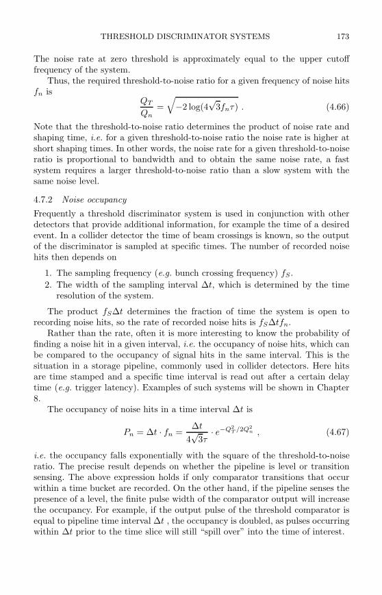
THRESHOLD DISCRIMINATOR SYSTEMS 173
The noise rate at zero threshold is approximately equal to the upper cutofffrequency of the system.
Thus, the required threshold-to-noise ratio for a given frequency of noise hitsfn is
QT
Qn=
√
−2 log(4√
3fnτ) . (4.66)
Note that the threshold-to-noise ratio determines the product of noise rate andshaping time, i.e. for a given threshold-to-noise ratio the noise rate is higher atshort shaping times. In other words, the noise rate for a given threshold-to-noiseratio is proportional to bandwidth and to obtain the same noise rate, a fastsystem requires a larger threshold-to-noise ratio than a slow system with thesame noise level.
4.7.2 Noise occupancy
Frequently a threshold discriminator system is used in conjunction with otherdetectors that provide additional information, for example the time of a desiredevent. In a collider detector the time of beam crossings is known, so the outputof the discriminator is sampled at specific times. The number of recorded noisehits then depends on
1. The sampling frequency (e.g. bunch crossing frequency) fS .
2. The width of the sampling interval ∆t, which is determined by the timeresolution of the system.
The product fS∆t determines the fraction of time the system is open torecording noise hits, so the rate of recorded noise hits is fS∆tfn.
Rather than the rate, often it is more interesting to know the probability offinding a noise hit in a given interval, i.e. the occupancy of noise hits, which canbe compared to the occupancy of signal hits in the same interval. This is thesituation in a storage pipeline, commonly used in collider detectors. Here hitsare time stamped and a specific time interval is read out after a certain delaytime (e.g. trigger latency). Examples of such systems will be shown in Chapter8.
The occupancy of noise hits in a time interval ∆t is
Pn = ∆t · fn =∆t
4√
3τ· e−Q2
T /2Q2
n , (4.67)
i.e. the occupancy falls exponentially with the square of the threshold-to-noiseratio. The precise result depends on whether the pipeline is level or transitionsensing. The above expression holds if only comparator transitions that occurwithin a time bucket are recorded. On the other hand, if the pipeline senses thepresence of a level, the finite pulse width of the comparator output will increasethe occupancy. For example, if the output pulse of the threshold comparator isequal to pipeline time interval ∆t , the occupancy is doubled, as pulses occurringwithin ∆t prior to the time slice will still “spill over” into the time of interest.
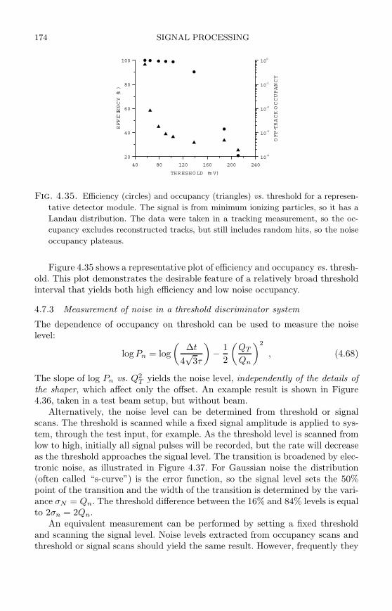
174 SIGNAL PROCESSING
40 80 120 160 200 240
THRESHOLD (m V)
20
40
60
80
100
EFFICIENCY(%
)
10-4
10-3
10-2
10-1
100
OFF-TRACKOCCUPANCY
Fig. 4.35. Efficiency (circles) and occupancy (triangles) vs. threshold for a represen-
tative detector module. The signal is from minimum ionizing particles, so it has a
Landau distribution. The data were taken in a tracking measurement, so the oc-
cupancy excludes reconstructed tracks, but still includes random hits, so the noise
occupancy plateaus.
Figure 4.35 shows a representative plot of efficiency and occupancy vs. thresh-old. This plot demonstrates the desirable feature of a relatively broad thresholdinterval that yields both high efficiency and low noise occupancy.
4.7.3 Measurement of noise in a threshold discriminator system
The dependence of occupancy on threshold can be used to measure the noiselevel:
log Pn = log
(
∆t
4√
3τ
)
− 1
2
(
QT
Qn
)2
, (4.68)
The slope of log Pn vs. Q2T yields the noise level, independently of the details of
the shaper, which affect only the offset. An example result is shown in Figure4.36, taken in a test beam setup, but without beam.
Alternatively, the noise level can be determined from threshold or signalscans. The threshold is scanned while a fixed signal amplitude is applied to sys-tem, through the test input, for example. As the threshold level is scanned fromlow to high, initially all signal pulses will be recorded, but the rate will decreaseas the threshold approaches the signal level. The transition is broadened by elec-tronic noise, as illustrated in Figure 4.37. For Gaussian noise the distribution(often called “s-curve”) is the error function, so the signal level sets the 50%point of the transition and the width of the transition is determined by the vari-ance σN = Qn. The threshold difference between the 16% and 84% levels is equalto 2σn = 2Qn.
An equivalent measurement can be performed by setting a fixed thresholdand scanning the signal level. Noise levels extracted from occupancy scans andthreshold or signal scans should yield the same result. However, frequently they
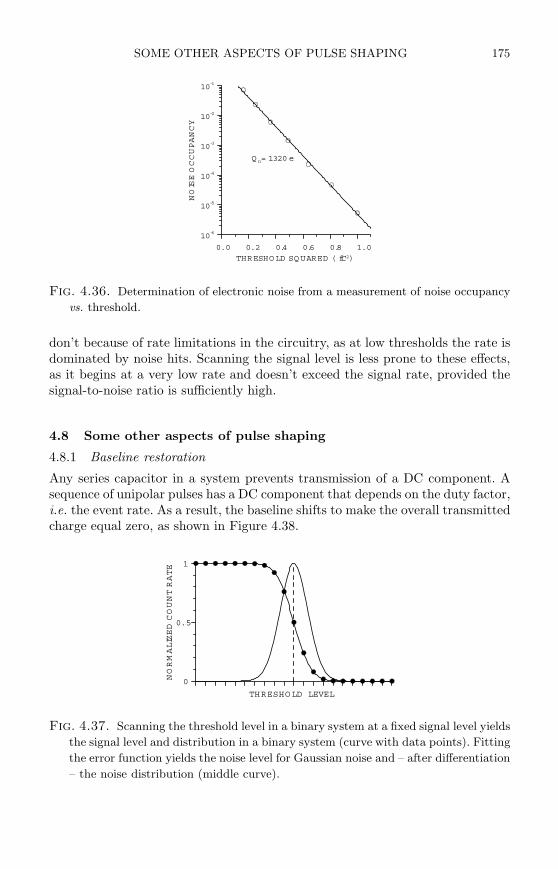
SOME OTHER ASPECTS OF PULSE SHAPING 175
0.0 0.2 0.4 0.6 0.8 1.0
THRESHOLD SQUARED ( fC2)
10-6
10-5
10-4
10-3
10-2
10-1
NOISEOCCUPANCY
Q n= 1320 e
Fig. 4.36. Determination of electronic noise from a measurement of noise occupancy
vs. threshold.
don’t because of rate limitations in the circuitry, as at low thresholds the rate isdominated by noise hits. Scanning the signal level is less prone to these effects,as it begins at a very low rate and doesn’t exceed the signal rate, provided thesignal-to-noise ratio is sufficiently high.
4.8 Some other aspects of pulse shaping
4.8.1 Baseline restoration
Any series capacitor in a system prevents transmission of a DC component. Asequence of unipolar pulses has a DC component that depends on the duty factor,i.e. the event rate. As a result, the baseline shifts to make the overall transmittedcharge equal zero, as shown in Figure 4.38.
THRESHOLD LEVEL
0
0.5
1
NORMALIZEDCOUNTRATE
Fig. 4.37. Scanning the threshold level in a binary system at a fixed signal level yields
the signal level and distribution in a binary system (curve with data points). Fitting
the error function yields the noise level for Gaussian noise and – after differentiation
– the noise distribution (middle curve).
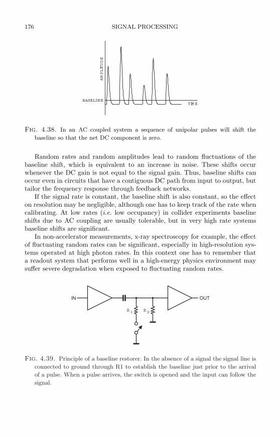
176 SIGNAL PROCESSING
AMPLITUDE
TIM EBASELINE
Fig. 4.38. In an AC coupled system a sequence of unipolar pulses will shift the
baseline so that the net DC component is zero.
Random rates and random amplitudes lead to random fluctuations of thebaseline shift, which is equivalent to an increase in noise. These shifts occurwhenever the DC gain is not equal to the signal gain. Thus, baseline shifts canoccur even in circuits that have a contiguous DC path from input to output, buttailor the frequency response through feedback networks.
If the signal rate is constant, the baseline shift is also constant, so the effecton resolution may be negligible, although one has to keep track of the rate whencalibrating. At low rates (i.e. low occupancy) in collider experiments baselineshifts due to AC coupling are usually tolerable, but in very high rate systemsbaseline shifts are significant.
In non-accelerator measurements, x-ray spectroscopy for example, the effectof fluctuating random rates can be significant, especially in high-resolution sys-tems operated at high photon rates. In this context one has to remember thata readout system that performs well in a high-energy physics environment maysuffer severe degradation when exposed to fluctuating random rates.
IN OUT
R R1 2
Fig. 4.39. Principle of a baseline restorer. In the absence of a signal the signal line is
connected to ground through R1 to establish the baseline just prior to the arrival
of a pulse. When a pulse arrives, the switch is opened and the input can follow the
signal.
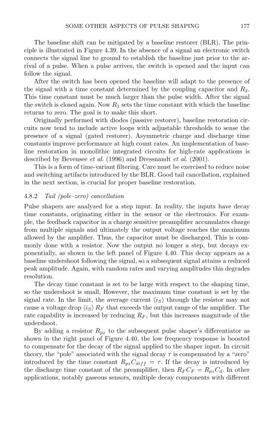
SOME OTHER ASPECTS OF PULSE SHAPING 177
The baseline shift can be mitigated by a baseline restorer (BLR). The prin-ciple is illustrated in Figure 4.39. In the absence of a signal an electronic switchconnects the signal line to ground to establish the baseline just prior to the ar-rival of a pulse. When a pulse arrives, the switch is opened and the input canfollow the signal.
After the switch has been opened the baseline will adapt to the presence ofthe signal with a time constant determined by the coupling capacitor and R2.This time constant must be much larger than the pulse width. After the signalthe switch is closed again. Now R1 sets the time constant with which the baselinereturns to zero. The goal is to make this short.
Originally performed with diodes (passive restorer), baseline restoration cir-cuits now tend to include active loops with adjustable thresholds to sense thepresence of a signal (gated restorer). Asymmetric charge and discharge timeconstants improve performance at high count rates. An implementation of base-line restoration in monolithic integrated circuits for high-rate applications isdescribed by Bevensee et al. (1996) and Dressnandt et al. (2001).
This is a form of time-variant filtering. Care must be exercised to reduce noiseand switching artifacts introduced by the BLR. Good tail cancellation, explainedin the next section, is crucial for proper baseline restoration.
4.8.2 Tail (pole–zero) cancellation
Pulse shapers are analyzed for a step input. In reality, the inputs have decaytime constants, originating either in the sensor or the electronics. For exam-ple, the feedback capacitor in a charge sensitive preamplifier accumulates chargefrom multiple signals and ultimately the output voltage reaches the maximumallowed by the amplifier. Thus, the capacitor must be discharged. This is com-monly done with a resistor. Now the output no longer a step, but decays ex-ponentially, as shown in the left panel of Figure 4.40. This decay appears as abaseline undershoot following the signal, so a subsequent signal attains a reducedpeak amplitude. Again, with random rates and varying amplitudes this degradesresolution.
The decay time constant is set to be large with respect to the shaping time,so the undershoot is small. However, the maximum time constant is set by thesignal rate. In the limit, the average current 〈iS〉 through the resistor may notcause a voltage drop 〈iS〉RF that exceeds the output range of the amplifier. Therate capability is increased by reducing RF , but this increases magnitude of theundershoot.
By adding a resistor Rpz to the subsequent pulse shaper’s differentiator asshown in the right panel of Figure 4.40, the low frequency response is boostedto compensate for the decay of the signal applied to the shaper input. In circuittheory, the “pole” associated with the signal decay τ is compensated by a “zero”introduced by the time constant RpzCdiff = τ . If the decay is introduced bythe discharge time constant of the preamplifier, then RF CF = RpzCd. In otherapplications, notably gaseous sensors, multiple decay components with different
178 SIGNAL PROCESSING
PO LE-ZERO CO M PENSATED
CF
RF
CdiffRdiff
Rpz
TIM E
PREAMPOUTPUT
TIM E
SHAPEROUTPUT
TIM E
SHAPEROUTPUT
Fig. 4.40. A long decay time constant is transposed on the baseline and reduces the
amplitude of the next pulse. Adding equalization circuitry to boost the frequency
response in the appropriate range yields a constant baseline.
time constants are common. Multiple cancellation circuits can be introduced todeal with this. However, this only compensates for purely exponential decays.
An alternative to resistive discharge in the preamplifier is to use pulsed resetcircuits (optical or transistor) that discharge the feedback capacitor when theoutput approaches the voltage limit. The discharge spike must be suppressed,but since the output of the preamplifier is a sequence of superimposed steps,pole–zero cancellation is not necessary.
4.8.3 Bipolar vs. unipolar shaping
As explained in the discussion on baseline restorers, a sequence of unipolar pulsespassing through an AC coupled system leads to baseline shifts. This can beavoided by using pulse shapers with both a positive and negative lobe, so thatthe net charge of the shaped pulse is zero (although the peak amplitude is stillproportional to signal charge). Generally, bipolar shapers can be constructed byadding a second differentiator to a unipolar shaper. Using equal time constantsτ in a CR-CR-RC shaper yields the pulse shape
TIMING MEASUREMENTS 179
0 2 4 6 8
NORM ALIZED TIM E t/
-0.1
0
0.1
0.2
0.3
0.4
AMPLITUDE
BASELINE
Fig. 4.41. Unipolar and bipolar pulses from CR-RC and CR2-RC shapers. The time
is normalized to the integrator and differentiator time constants τ .
V (t) = V0
[
t
τ− 1
2
(
t
τ
)2]
e−t/τ , (4.69)
which is plotted in Figure 4.41 together with the original CR-RC unipolar pulseshape for comparison. Since the second CR stage isn’t an ideal differentiator, thezero crossing doesn’t occur at the peak of the unipolar pulse. The reduction inpeak amplitude visible in Figure 4.41 accounts for most of the 38% degradationin ENC relative to a CR-RC shaper, as the more rapid low-frequency roll-offhardly affects the noise bandwidth.
Bipolar shapers are usually frowned upon by purists, as the electronic noiseis typically 25 – 50% worse than for the corresponding unipolar shaper. However,bipolar shaping eliminates rate dependent baseline shifts (as the DC componentis zero) and pole–zero adjustment is less critical. Not all systems require optimumelectronic noise, so operational robustness and user convenience may override.The most important feature of bipolar shapers may be the added suppression oflow-frequency noise (see Chapter 9). In systems subject to external interferencethis can be crucial, so in practical systems “inferior” shapers often yield superiorresults.
4.9 Timing measurements
Pulse height measurements discussed up to now emphasize measurement of sig-nal charge. Timing measurements seek to optimize the determination of the timeof occurrence. Although, as in amplitude measurements, signal-to-noise ratio isimportant, the determining parameter is not signal-to-noise, but slope-to-noiseratio. This is illustrated in Figure 4.42, which shows the leading edge of a pulsefed into a threshold discriminator (comparator), a “leading edge trigger”. The
180 SIGNAL PROCESSING
TIME TIME
AMPLITUDE
AMPLITUDE
V
V
T
T
2
2
n
t
dVdt
= max
Fig. 4.42. Fluctuations in signal amplitude crossing a threshold translate into tim-
ing fluctuations (left). With realistic pulses the slope changes with amplitude, so
minimum timing jitter occurs with the trigger level at the maximum slope.
instantaneous signal level is modulated by noise, where the variations are indi-cated by the shaded band. Because of these fluctuations, the time of thresholdcrossing fluctuates. By simple geometrical projection, the timing variance, or“jitter”, is
σt =σn
dVdt
∣
∣
VT
≈ trS/N
. (4.70)
Typically, the leading edge is not linear, so the optimum trigger level is the pointof maximum slope, as shown in the second panel of Figure 4.42.
4.9.1 Pulse shaping in timing systems
Consider a system whose bandwidth is determined by a single RC filter. The timeconstant of the RC low-pass filter determines the rise time (and hence dV/dt)and the amplifier bandwidth (and hence the noise). The time dependence of thesignal
V (t) = V0(1 − e−t/τ ) . (4.71)
The rise time is commonly expressed as the interval between the points of 10%and 90% amplitude, so tr = 2.2τ . In terms of bandwidth
tr = 2.2τ =2.2
2πfu=
0.35
fu. (4.72)
For example, an oscilloscope with 100MHz bandwidth has 3.5 ns rise time. In acascade of amplifiers the individual rise times add in quadrature
tr ≈√
t2r1 + t2r2 + . . . + t2rn . (4.73)
These rules only apply to amplifiers with nRC-integrator responses, whichis usually the case in amplifiers, as was shown in Chapter 2. However, digital
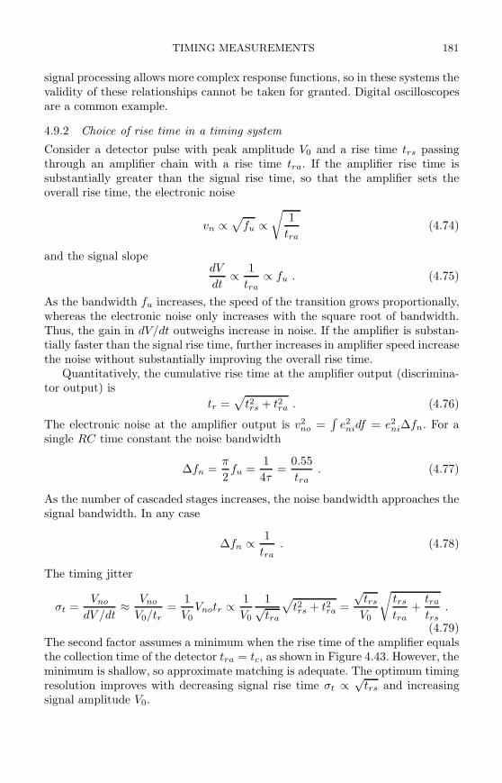
TIMING MEASUREMENTS 181
signal processing allows more complex response functions, so in these systems thevalidity of these relationships cannot be taken for granted. Digital oscilloscopesare a common example.
4.9.2 Choice of rise time in a timing system
Consider a detector pulse with peak amplitude V0 and a rise time trs passingthrough an amplifier chain with a rise time tra. If the amplifier rise time issubstantially greater than the signal rise time, so that the amplifier sets theoverall rise time, the electronic noise
vn ∝√
fu ∝√
1
tra(4.74)
and the signal slopedV
dt∝ 1
tra∝ fu . (4.75)
As the bandwidth fu increases, the speed of the transition grows proportionally,whereas the electronic noise only increases with the square root of bandwidth.Thus, the gain in dV/dt outweighs increase in noise. If the amplifier is substan-tially faster than the signal rise time, further increases in amplifier speed increasethe noise without substantially improving the overall rise time.
Quantitatively, the cumulative rise time at the amplifier output (discrimina-tor output) is
tr =√
t2rs + t2ra . (4.76)
The electronic noise at the amplifier output is v2no =
∫
e2nidf = e2
ni∆fn. For asingle RC time constant the noise bandwidth
∆fn =π
2fu =
1
4τ=
0.55
tra. (4.77)
As the number of cascaded stages increases, the noise bandwidth approaches thesignal bandwidth. In any case
∆fn ∝ 1
tra. (4.78)
The timing jitter
σt =Vno
dV /dt≈ Vno
V0/tr=
1
V0Vnotr ∝ 1
V0
1√tra
√
t2rs + t2ra =
√trs
V0
√
trs
tra+
tra
trs.
(4.79)The second factor assumes a minimum when the rise time of the amplifier equalsthe collection time of the detector tra = tc, as shown in Figure 4.43. However, theminimum is shallow, so approximate matching is adequate. The optimum timingresolution improves with decreasing signal rise time σt ∝ √
trs and increasingsignal amplitude V0.

182 SIGNAL PROCESSING
0.1 1 10AM PLIFIER RISE TIM E / SIGNAL RISE TIM E
TIMERESOLUTION
Fig. 4.43. The timing jitter assumes a minimum when the amplifier rise time matches
the signal rise time.
The integration time should be chosen to match the rise time, but how shouldthe differentiation time be chosen? As shown in Figure 4.2, the loss in signalcan be appreciable even when the differentiation time constant is significantlygreater than the integration time constant, e.g. > 20% for τdiff /τint = 10. Sincethe time resolution improves directly with increasing peak signal amplitude, thedifferentiation time should be set as large as allowed by the required pulse rate.
4.9.3 Time walk
Up to now we have considered timing jitter, i.e. the timing variation for a fixedamplitude. In addition, the time at which the signal crosses a fixed thresholddepends on pulse amplitude. As the amplitude varies, the timing signal shifts,so variations in signal amplitude will broaden the timing distribution. This phe-nomenon is called “time walk” and is illustrated in Figure 4.44.
As a result, the accuracy of timing measurement is limited by the combinationof jitter (due to noise) and time walk (due to amplitude variations). If the risetime is known, “time walk” can be compensated in software event-by-event bymeasuring the pulse height and correcting the time measurement. This techniquefails if both amplitude and rise time vary, as is common. Recall, that in semi-conductor sensors the rise time combines both electron and hole components, sothe slope has two components. In hardware, time walk can be reduced by settingthe threshold to the lowest practical level, or by using amplitude compensatingcircuitry, which will be described in the following sections.
Before going into a detailed discussion of timing techniques we should bear inmind that many systems do not require the “perfect” timing system. In charged-particle tracking detectors all particles traverse the sensor, so the relative con-tribution of electrons and holes is always the same and rise-time compensationis not necessary. Minimum ionizing particles all deposit the same average energy
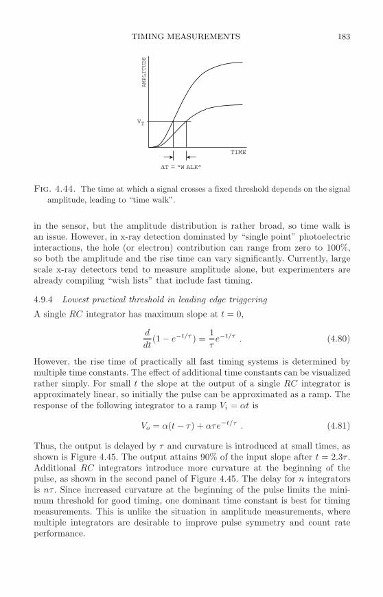
TIMING MEASUREMENTS 183
TIME
AMPLITUDE
VT
T = “W ALK”
Fig. 4.44. The time at which a signal crosses a fixed threshold depends on the signal
amplitude, leading to “time walk”.
in the sensor, but the amplitude distribution is rather broad, so time walk isan issue. However, in x-ray detection dominated by “single point” photoelectricinteractions, the hole (or electron) contribution can range from zero to 100%,so both the amplitude and the rise time can vary significantly. Currently, largescale x-ray detectors tend to measure amplitude alone, but experimenters arealready compiling “wish lists” that include fast timing.
4.9.4 Lowest practical threshold in leading edge triggering
A single RC integrator has maximum slope at t = 0,
d
dt(1 − e−t/τ ) =
1
τe−t/τ . (4.80)
However, the rise time of practically all fast timing systems is determined bymultiple time constants. The effect of additional time constants can be visualizedrather simply. For small t the slope at the output of a single RC integrator isapproximately linear, so initially the pulse can be approximated as a ramp. Theresponse of the following integrator to a ramp Vi = αt is
Vo = α(t − τ) + ατe−t/τ . (4.81)
Thus, the output is delayed by τ and curvature is introduced at small times, asshown is Figure 4.45. The output attains 90% of the input slope after t = 2.3τ .Additional RC integrators introduce more curvature at the beginning of thepulse, as shown in the second panel of Figure 4.45. The delay for n integratorsis nτ . Since increased curvature at the beginning of the pulse limits the mini-mum threshold for good timing, one dominant time constant is best for timingmeasurements. This is unlike the situation in amplitude measurements, wheremultiple integrators are desirable to improve pulse symmetry and count rateperformance.
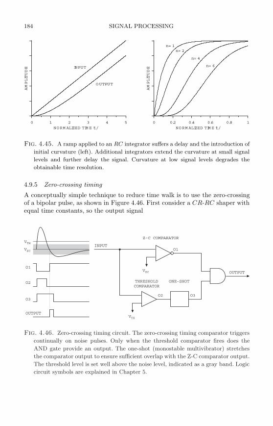
184 SIGNAL PROCESSING
0 1 2 3 4 5
NORM ALIZED TIM E t/
AMPLITUDE INPUT
OUTPUT
0 0.2 0.4 0.6 0.8 1
NORM ALIZED TIM E t/
AMPLITUDE
n= 1n= 2
n= 4
n= 6
Fig. 4.45. A ramp applied to an RC integrator suffers a delay and the introduction of
initial curvature (left). Additional integrators extend the curvature at small signal
levels and further delay the signal. Curvature at low signal levels degrades the
obtainable time resolution.
4.9.5 Zero-crossing timing
A conceptually simple technique to reduce time walk is to use the zero-crossingof a bipolar pulse, as shown in Figure 4.46. First consider a CR-RC shaper withequal time constants, so the output signal
V
V
V
V
TH
ZC
ZC
TH
ONE-SHOTTHRESHOLDCOMPARATOR
O2 O3
O1
OUTPUT
INPUT
O1
O2
O3
OUTPUT
Z-C COMPARATOR
Fig. 4.46. Zero-crossing timing circuit. The zero-crossing timing comparator triggers
continually on noise pulses. Only when the threshold comparator fires does the
AND gate provide an output. The one-shot (monostable multivibrator) stretches
the comparator output to ensure sufficient overlap with the Z-C comparator output.
The threshold level is set well above the noise level, indicated as a gray band. Logic
circuit symbols are explained in Chapter 5.
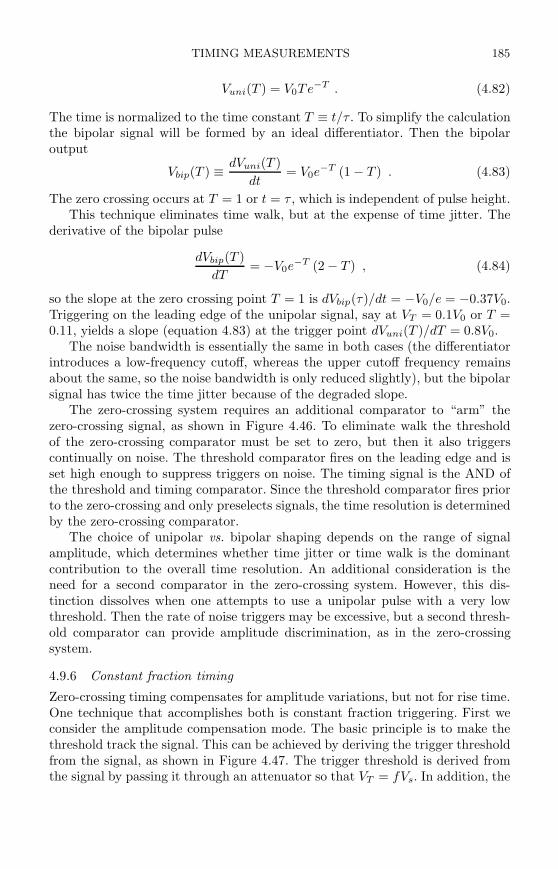
TIMING MEASUREMENTS 185
Vuni(T ) = V0Te−T . (4.82)
The time is normalized to the time constant T ≡ t/τ . To simplify the calculationthe bipolar signal will be formed by an ideal differentiator. Then the bipolaroutput
Vbip(T ) ≡ dVuni(T )
dt= V0e
−T (1 − T ) . (4.83)
The zero crossing occurs at T = 1 or t = τ , which is independent of pulse height.This technique eliminates time walk, but at the expense of time jitter. The
derivative of the bipolar pulse
dVbip(T )
dT= −V0e
−T (2 − T ) , (4.84)
so the slope at the zero crossing point T = 1 is dVbip(τ)/dt = −V0/e = −0.37V0.Triggering on the leading edge of the unipolar signal, say at VT = 0.1V0 or T =0.11, yields a slope (equation 4.83) at the trigger point dVuni(T )/dT = 0.8V0.
The noise bandwidth is essentially the same in both cases (the differentiatorintroduces a low-frequency cutoff, whereas the upper cutoff frequency remainsabout the same, so the noise bandwidth is only reduced slightly), but the bipolarsignal has twice the time jitter because of the degraded slope.
The zero-crossing system requires an additional comparator to “arm” thezero-crossing signal, as shown in Figure 4.46. To eliminate walk the thresholdof the zero-crossing comparator must be set to zero, but then it also triggerscontinually on noise. The threshold comparator fires on the leading edge and isset high enough to suppress triggers on noise. The timing signal is the AND ofthe threshold and timing comparator. Since the threshold comparator fires priorto the zero-crossing and only preselects signals, the time resolution is determinedby the zero-crossing comparator.
The choice of unipolar vs. bipolar shaping depends on the range of signalamplitude, which determines whether time jitter or time walk is the dominantcontribution to the overall time resolution. An additional consideration is theneed for a second comparator in the zero-crossing system. However, this dis-tinction dissolves when one attempts to use a unipolar pulse with a very lowthreshold. Then the rate of noise triggers may be excessive, but a second thresh-old comparator can provide amplitude discrimination, as in the zero-crossingsystem.
4.9.6 Constant fraction timing
Zero-crossing timing compensates for amplitude variations, but not for rise time.One technique that accomplishes both is constant fraction triggering. First weconsider the amplitude compensation mode. The basic principle is to make thethreshold track the signal. This can be achieved by deriving the trigger thresholdfrom the signal, as shown in Figure 4.47. The trigger threshold is derived fromthe signal by passing it through an attenuator so that VT = fVs. In addition, the
186 SIGNAL PROCESSING
ATTENUATOR
xf
INPUT
THRESHOLD
DELAY td
t
t
t
V
fV
V
0
0
T
OUTPUT
td
INPUT
THRESHOLD
Fig. 4.47. Principle of a constant fraction timing circuit. The threshold VT of a timing
discriminator is derived from the pulse amplitude to compensate for time walk.
signal applied to the comparator input is delayed so that the transition occursafter the threshold signal has reached its maximum value VT = fV0. Delay linescan be implemented in integrated circuits as strip line spirals (Simpson et al.1996), but require substantial area. As will be shown below, the circuit alsofunctions well with delays less than the rise time, which also provide rise timecompensation.
For simplicity assume a linear leading edge
V (t) =t
trV0 for t ≤ tr
V (t) = V0 for t > tr , (4.85)
so the signal applied to the input is
V (t) =t − td
trV0 . (4.86)
When the input signal crosses the threshold level
fV0 =t − td
trV0 (4.87)
and – provided that the delay time is greater than the rise time td > tr – thecomparator fires at the time
t = ftr + td (4.88)
at a constant fraction of the rise time independent of peak amplitude. In reality,the signal pulse usually attains a cusp, so the condition for the delay is that isbe approximately equal to the rise time.
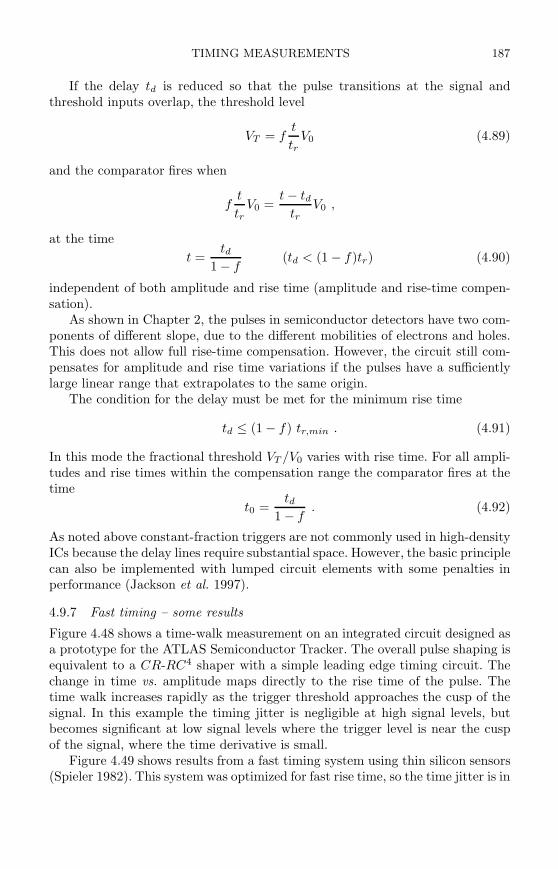
TIMING MEASUREMENTS 187
If the delay td is reduced so that the pulse transitions at the signal andthreshold inputs overlap, the threshold level
VT = ft
trV0 (4.89)
and the comparator fires when
ft
trV0 =
t − tdtr
V0 ,
at the time
t =td
1 − f(td < (1 − f)tr) (4.90)
independent of both amplitude and rise time (amplitude and rise-time compen-sation).
As shown in Chapter 2, the pulses in semiconductor detectors have two com-ponents of different slope, due to the different mobilities of electrons and holes.This does not allow full rise-time compensation. However, the circuit still com-pensates for amplitude and rise time variations if the pulses have a sufficientlylarge linear range that extrapolates to the same origin.
The condition for the delay must be met for the minimum rise time
td ≤ (1 − f) tr,min . (4.91)
In this mode the fractional threshold VT /V0 varies with rise time. For all ampli-tudes and rise times within the compensation range the comparator fires at thetime
t0 =td
1 − f. (4.92)
As noted above constant-fraction triggers are not commonly used in high-densityICs because the delay lines require substantial space. However, the basic principlecan also be implemented with lumped circuit elements with some penalties inperformance (Jackson et al. 1997).
4.9.7 Fast timing – some results
Figure 4.48 shows a time-walk measurement on an integrated circuit designed asa prototype for the ATLAS Semiconductor Tracker. The overall pulse shaping isequivalent to a CR-RC4 shaper with a simple leading edge timing circuit. Thechange in time vs. amplitude maps directly to the rise time of the pulse. Thetime walk increases rapidly as the trigger threshold approaches the cusp of thesignal. In this example the timing jitter is negligible at high signal levels, butbecomes significant at low signal levels where the trigger level is near the cuspof the signal, where the time derivative is small.
Figure 4.49 shows results from a fast timing system using thin silicon sensors(Spieler 1982). This system was optimized for fast rise time, so the time jitter is in
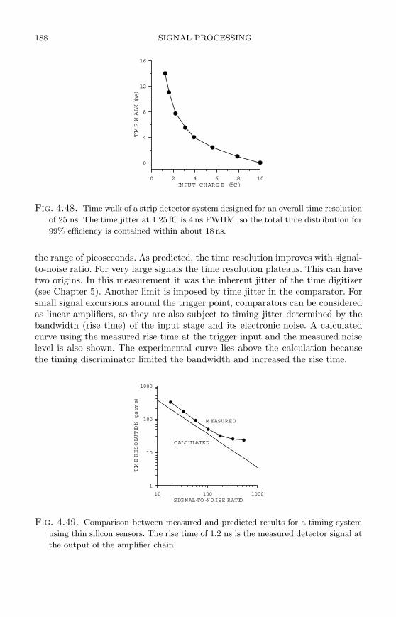
188 SIGNAL PROCESSING
0 2 4 6 8 10INPUT CHARGE (fC)
0
4
8
12
16
TIMEWALK(ns)
Fig. 4.48. Time walk of a strip detector system designed for an overall time resolution
of 25 ns. The time jitter at 1.25 fC is 4 ns FWHM, so the total time distribution for
99% efficiency is contained within about 18 ns.
the range of picoseconds. As predicted, the time resolution improves with signal-to-noise ratio. For very large signals the time resolution plateaus. This can havetwo origins. In this measurement it was the inherent jitter of the time digitizer(see Chapter 5). Another limit is imposed by time jitter in the comparator. Forsmall signal excursions around the trigger point, comparators can be consideredas linear amplifiers, so they are also subject to timing jitter determined by thebandwidth (rise time) of the input stage and its electronic noise. A calculatedcurve using the measured rise time at the trigger input and the measured noiselevel is also shown. The experimental curve lies above the calculation becausethe timing discriminator limited the bandwidth and increased the rise time.
10 100 1000SIGNAL-TO-NOISE RATIO
1
10
100
1000
TIMERESOLUTION(psrms)
M EASURED
CALCULATED
Fig. 4.49. Comparison between measured and predicted results for a timing system
using thin silicon sensors. The rise time of 1.2 ns is the measured detector signal at
the output of the amplifier chain.
REFERENCES 189
References
Bevensee, B. et al. (1996). An amplifier-shaper-discriminator with baselinerestoration for the ATLAS Transition Radiation Tracker. IEEE Trans. Nucl.Sci. 43/3 (1996) 1725–1731
Choong, W.-S. et al. (2002). A compact 16-module camera using 64-pixelCsI(Tl)/Si p-i-n photodiode imaging modules. IEEE Trans. Nucl. Sci. NS-49/5 (2002) 2228–2235
Dressnandt, N. et al. (2001). Implementation of the ASDBLR straw tube read-out ASIC in DMILL technology. IEEE Trans. Nucl. Sci. 48/4 (2001) 1239–1243
Gatti, E. and Manfredi, P.F. (1986). Processing the signals from solid-statedetectors in elementary particle physics. Riv. Nuovo Cimento 9/1 (1986) 1–146
Gillespie, A.B. (1953). Signal, Noise, and Resolution in Nuclear Counter Am-plifiers. Pergamon Press, New York
Goulding, F.S. (1972). Pulse shaping in low-noise nuclear amplifiers: a physicalapproach to noise analysis. Nucl. Instr. Meth. 100 (1972) 493–504
Goulding, F.S. and Landis, D.A. (1982). Signal processing for semiconductordetectors. IEEE Trans. Nucl. Sci. NS-29/3 (1982) 1125–1141
Holland, S.E., Wang, N.W., and Moses, W.W. (1997). Development of lownoise, back-side illuminated silicon photodiode arrays. IEEE Trans. Nucl. Sci.NS-44/3 (1997) 443–447
Jackson, R.G. et al. (1997). Integrated constant fraction discriminator shapingtechniques for the PHENIX lead-scintillator calorimeter. IEEE Trans. Nucl.Sci. NS-44/3 (1997) 303–307
Kansy, R.J. (1980). Response of a correlated double sampling circuit to 1/fnoise. IEEE J. Solid-State Circuits SC-15/3 (1980) 373–375
Knoll, G.F. (2000). Radiation Detection and Measurement (3rd edn). Wiley,New York, ISBN 0-471-07338-5, QC 787.C6K56
Kowalski, E. (1970). Nuclear Electronics. Springer Verlag, New York, 1970Krieger, B., Kipnis, I. and Ludewigt, B.A. (1998). XPS: a multi-channel pream-plifier – shaper IC for x-ray spectroscopy. IEEE Trans. Nucl. Sci. 45/3 (1998)732–734
Lee, T-H. et al. (2002). Analysis of 1/f noise in CMOS preamplifier with CDScircuit. IEEE Trans. Nucl. Sci. NS-49/4 (2002) 1819–1823
Ludewigt, B. et al. (1994). A high rate, low noise, x-ray silicon strip detectorsystem. IEEE Trans. Nucl. Sci. NS-41/4 (1994) 1037–1041
Ludewigt, B. et al. (1996). Progress in multi-element silicon detectors for syn-chrotron XRF applications. IEEE Trans. Nucl. Sci. NS-43/3 (1996) 1442–1445
Radeka, V. (1972). Trapezoidal filtering of signals from large germanium detec-tors at high rates. Nucl. Instr. Meth. 99 (1972) 525–539
Radeka, V. (1974). Signal, noise and resolution in position-sensitive detectors.IEEE Trans. Nucl. Sci. NS-21 (1974) 51–64

190 SIGNAL PROCESSING
Rice, S.O. (1944). Mathematical analysis of random noise. Bell System Techni-cal Journal 23 (1944) 282–332 and 24 (1945) 46–156
Seller, P. (1996). Noise analysis in linear electronic circuits. Nucl. Instr. Meth.A376 (1996) 229–241
Simpson, M.L. et al. (1996). A monolithic, constant-fraction discriminator usingdistributed R-C delay line shaping. IEEE Trans. Nucl. Sci. NS-43/3 (1996)1695–1699
Spieler, H. (1982). Fast timing methods for semiconductor detectors. IEEETrans. Nucl. Sci. NS-29/3 (1982) 1142–1158
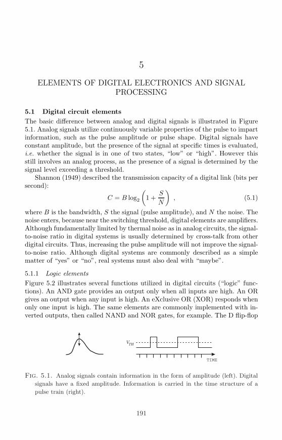
5
ELEMENTS OF DIGITAL ELECTRONICS AND SIGNAL
PROCESSING
5.1 Digital circuit elements
The basic difference between analog and digital signals is illustrated in Figure5.1. Analog signals utilize continuously variable properties of the pulse to impartinformation, such as the pulse amplitude or pulse shape. Digital signals haveconstant amplitude, but the presence of the signal at specific times is evaluated,i.e. whether the signal is in one of two states, “low” or “high”. However thisstill involves an analog process, as the presence of a signal is determined by thesignal level exceeding a threshold.
Shannon (1949) described the transmission capacity of a digital link (bits persecond):
C = B log2
(
1 +S
N
)
, (5.1)
where B is the bandwidth, S the signal (pulse amplitude), and N the noise. Thenoise enters, because near the switching threshold, digital elements are amplifiers.Although fundamentally limited by thermal noise as in analog circuits, the signal-to-noise ratio in digital systems is usually determined by cross-talk from otherdigital circuits. Thus, increasing the pulse amplitude will not improve the signal-to-noise ratio. Although digital systems are commonly described as a simplematter of “yes” or “no”, real systems must also deal with “maybe”.
5.1.1 Logic elements
Figure 5.2 illustrates several functions utilized in digital circuits (“logic” func-tions). An AND gate provides an output only when all inputs are high. An ORgives an output when any input is high. An eXclusive OR (XOR) responds whenonly one input is high. The same elements are commonly implemented with in-verted outputs, then called NAND and NOR gates, for example. The D flip-flop
TIME
VTH
Fig. 5.1. Analog signals contain information in the form of amplitude (left). Digital
signals have a fixed amplitude. Information is carried in the time structure of a
pulse train (right).
191
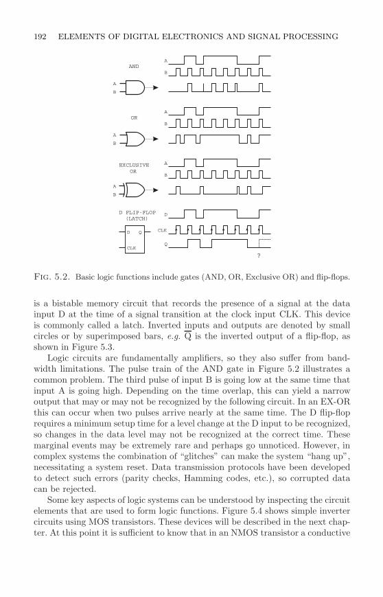
192 ELEMENTS OF DIGITAL ELECTRONICS AND SIGNAL PROCESSING
AND
OR
EXCLUSIVEOR
D FLIP-FLOP(LATCH)
D
CLK
Q
A
A
A
B
B
B
A
B
A
B
A
B
D
CLK
Q
?
Fig. 5.2. Basic logic functions include gates (AND, OR, Exclusive OR) and flip-flops.
is a bistable memory circuit that records the presence of a signal at the datainput D at the time of a signal transition at the clock input CLK. This deviceis commonly called a latch. Inverted inputs and outputs are denoted by smallcircles or by superimposed bars, e.g. Q is the inverted output of a flip-flop, asshown in Figure 5.3.
Logic circuits are fundamentally amplifiers, so they also suffer from band-width limitations. The pulse train of the AND gate in Figure 5.2 illustrates acommon problem. The third pulse of input B is going low at the same time thatinput A is going high. Depending on the time overlap, this can yield a narrowoutput that may or may not be recognized by the following circuit. In an EX-ORthis can occur when two pulses arrive nearly at the same time. The D flip-floprequires a minimum setup time for a level change at the D input to be recognized,so changes in the data level may not be recognized at the correct time. Thesemarginal events may be extremely rare and perhaps go unnoticed. However, incomplex systems the combination of “glitches” can make the system “hang up”,necessitating a system reset. Data transmission protocols have been developedto detect such errors (parity checks, Hamming codes, etc.), so corrupted datacan be rejected.
Some key aspects of logic systems can be understood by inspecting the circuitelements that are used to form logic functions. Figure 5.4 shows simple invertercircuits using MOS transistors. These devices will be described in the next chap-ter. At this point it is sufficient to know that in an NMOS transistor a conductive
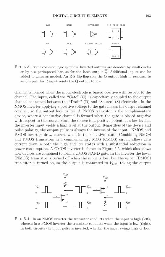
DIGITAL CIRCUIT ELEMENTS 193
AND NAND
OR NOR
INVERTER R-S FLIP-FLOP
LATCH
S
D
R
CLK
Q
Q
Q
Q
EXCLUSIVE OR
Fig. 5.3. Some common logic symbols. Inverted outputs are denoted by small circles
or by a superimposed bar, as for the latch output Q. Additional inputs can be
added to gates as needed. An R-S flip-flop sets the Q output high in response to
an S input. An R input resets the Q output to low.
channel is formed when the input electrode is biased positive with respect to thechannel. The input, called the “Gate” (G), is capacitively coupled to the outputchannel connected between the “Drain” (D) and “Source” (S) electrodes. In theNMOS inverter applying a positive voltage to the gate makes the output channelconduct, so the output level is low. A PMOS transistor is the complementarydevice, where a conductive channel is formed when the gate is biased negativewith respect to the source. Since the source is at positive potential, a low level atthe inverter input yields a high level at the output. Regardless of the device andpulse polarity, the output pulse is always the inverse of the input. NMOS andPMOS inverters draw current when in their “active” state. Combining NMOSand PMOS transistors in a complementary MOS (CMOS) circuit allows zerocurrent draw in both the high and low states with a substantial reduction inpower consumption. A CMOS inverter is shown in Figure 5.5, which also showshow devices are combined to form a CMOS NAND gate. In the inverter the lower(NMOS) transistor is turned off when the input is low, but the upper (PMOS)transistor is turned on, so the output is connected to VDD , taking the output
V
V
V V
V
V
VV
DD
DD
DD DD
DD
DD
DDDD
0 0
0
0
00
GD
S
GS
D
Fig. 5.4. In an NMOS inverter the transistor conducts when the input is high (left),
whereas in a PMOS inverter the transistor conducts when the input is low (right).
In both circuits the input pulse is inverted, whether the input swings high or low.
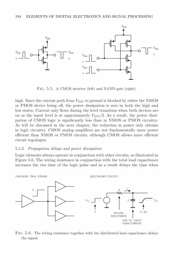
194 ELEMENTS OF DIGITAL ELECTRONICS AND SIGNAL PROCESSING
V
V
V
V
V
V
V
DD
DD
DD
DD
DD
DD
DD
0
0
00
0
Fig. 5.5. A CMOS inverter (left) and NAND gate (right).
high. Since the current path from VDD to ground is blocked by either the NMOSor PMOS device being off, the power dissipation is zero in both the high andlow states. Current only flows during the level transition when both devices areon as the input level is at approximately VDD/2. As a result, the power dissi-pation of CMOS logic is significantly less than in NMOS or PMOS circuitry.As will be discussed in the next chapter, the reduction in power only obtainsin logic circuitry. CMOS analog amplifiers are not fundamentally more powerefficient than NMOS or PMOS circuits, although CMOS allows more efficientcircuit topologies.
5.1.2 Propagation delays and power dissipation
Logic elements always operate in conjunction with other circuits, as illustrated inFigure 5.6. The wiring resistance in conjunction with the total load capacitanceincreases the rise time of the logic pulse and as a result delays the time when
CASCADED CMOS STAGES EQUIVALENT CIRCUIT
R
C
T T+t
V VTH TH
WIRINGRESISTANCE
SUM OF INPUTCAPACITANCES
i
0
V
Fig. 5.6. The wiring resistance together with the distributed load capacitance delays
the signal.
DIGITAL CIRCUIT ELEMENTS 195
the transition crosses the logic threshold. The power dissipated in the wiringresistance R is
P =
∫
i2(t)Rdt . (5.2)
The current flow during one transition
i(t) =V
Rexp
(
− t
RC
)
, (5.3)
so the dissipated power per transition (either positive or negative)
P =V 2
R
∞∫
0
exp
(
− t
RC
)
dt = CV 2 . (5.4)
If transitions occur at a frequency f , the power dissipation
P = fCV 2 . (5.5)
Thus, the power dissipation increases with clock frequency and the square of thelogic swing.
Fast logic is time-critical. It relies on logic operations from multiple pathscoming together at the right time. Valid results depend on maintaining mini-mum allowable overlaps (e.g. AND) and setup times (latches). Each logic circuithas a finite propagation delay, which depends on circuit loading, i.e. how manyloads the circuit has to drive. In addition, as illustrated in Figure 5.6 the wiringresistance and capacitive loads introduces delay. This depends on the number ofcircuits connected to a wire or trace, the length of the trace and the dielectricconstant of the substrate material. Relying on control of circuit and wiring delaysto maintain timing requires great care, as it depends on circuit variations andtemperature. In principle all of this can be simulated, but in complex systemsthere are too many combinations to test every one. A more robust solution isto use synchronous systems, where the timing of all transitions is determined bya master clock. Generally, this does not provide the utmost speed and requiressome additional circuitry, but increases reliability. Nevertheless, clever designersfrequently utilize asynchronous logic. Sometimes it succeeds . . . and sometimesit doesn’t.
5.1.3 Logic arrays
Commodity integrated circuits with basic logic blocks are readily available, e.g.with four NAND gates or two flip-flops in one package. These can be combinedto form simple digital systems. However, complex logic systems are no longerdesigned using individual gates. Instead, logic functions are described in a high-level language (e.g. VHDL), synthesized using design libraries, and implementedas custom ICs – “ASICs” (application specific ICs) – or programmable logicarrays. In these implementations the digital circuitry no longer appears as an
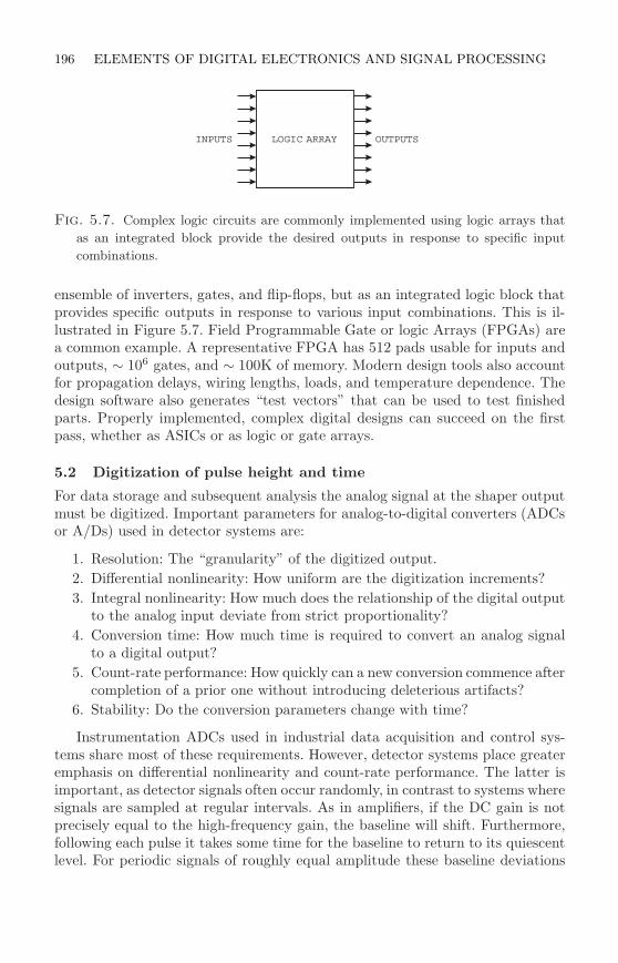
196 ELEMENTS OF DIGITAL ELECTRONICS AND SIGNAL PROCESSING
LOGIC ARRAYINPUTS OUTPUTS
Fig. 5.7. Complex logic circuits are commonly implemented using logic arrays that
as an integrated block provide the desired outputs in response to specific input
combinations.
ensemble of inverters, gates, and flip-flops, but as an integrated logic block thatprovides specific outputs in response to various input combinations. This is il-lustrated in Figure 5.7. Field Programmable Gate or logic Arrays (FPGAs) area common example. A representative FPGA has 512 pads usable for inputs andoutputs, ∼ 106 gates, and ∼ 100K of memory. Modern design tools also accountfor propagation delays, wiring lengths, loads, and temperature dependence. Thedesign software also generates “test vectors” that can be used to test finishedparts. Properly implemented, complex digital designs can succeed on the firstpass, whether as ASICs or as logic or gate arrays.
5.2 Digitization of pulse height and time
For data storage and subsequent analysis the analog signal at the shaper outputmust be digitized. Important parameters for analog-to-digital converters (ADCsor A/Ds) used in detector systems are:
1. Resolution: The “granularity” of the digitized output.
2. Differential nonlinearity: How uniform are the digitization increments?
3. Integral nonlinearity: How much does the relationship of the digital outputto the analog input deviate from strict proportionality?
4. Conversion time: How much time is required to convert an analog signalto a digital output?
5. Count-rate performance: How quickly can a new conversion commence aftercompletion of a prior one without introducing deleterious artifacts?
6. Stability: Do the conversion parameters change with time?
Instrumentation ADCs used in industrial data acquisition and control sys-tems share most of these requirements. However, detector systems place greateremphasis on differential nonlinearity and count-rate performance. The latter isimportant, as detector signals often occur randomly, in contrast to systems wheresignals are sampled at regular intervals. As in amplifiers, if the DC gain is notprecisely equal to the high-frequency gain, the baseline will shift. Furthermore,following each pulse it takes some time for the baseline to return to its quiescentlevel. For periodic signals of roughly equal amplitude these baseline deviations
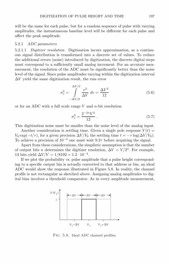
DIGITIZATION OF PULSE HEIGHT AND TIME 197
will be the same for each pulse, but for a random sequence of pulse with varyingamplitudes, the instantaneous baseline level will be different for each pulse andaffect the peak amplitude.
5.2.1 ADC parameters
5.2.1.1 Digitizer resolution Digitization incurs approximation, as a continu-ous signal distribution is transformed into a discrete set of values. To reducethe additional errors (noise) introduced by digitization, the discrete digital stepsmust correspond to a sufficiently small analog increment. For an accurate mea-surement, the resolution of the ADC must be significantly better than the noiselevel of the signal. Since pulse amplitudes varying within the digitization interval∆V yield the same digitization result, the rms error
σ2v =
∆V/2∫
−∆V/2
v2
∆Vdv =
∆V 2
12(5.6)
or for an ADC with a full scale range V and n-bit resolution
σ2v =
2−2nV 2
12. (5.7)
This digitization noise must be smaller than the noise level of the analog input.Another consideration is settling time. Given a single pole response V (t) =
V0 exp(−t/τ), for a given precision ∆V/V0 the settling time t = −τ log(∆V/V0).To achieve a precision of 10−4 one must wait 9.2τ before acquiring the signal.
Apart from these considerations, the simplistic assumption is that the numberof output bits n determines the digitizer resolution, ∆V = V/2n. For example,13 bits yield ∆V/V = 1/8192 = 1.2 · 10−4.
If we plot the probability vs. pulse amplitude that a pulse height correspond-ing to a specific output bin is actually converted to that address or bin, an idealADC would show the response illustrated in Figure 5.8. In reality, the channelprofile is not rectangular as sketched above. Assigning analog amplitudes to dig-ital bins involves a threshold comparator. As in every amplitude measurement,
V VV i ii +V
VV V
V
1
P V( )i
Fig. 5.8. Ideal ADC channel profiles.
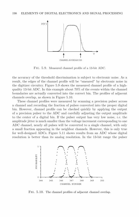
198 ELEMENTS OF DIGITAL ELECTRONICS AND SIGNAL PROCESSING
CHANNEL BOUNDARIES
P V( )
V
Fig. 5.9. Measured channel profile of a 13-bit ADC.
the accuracy of the threshold discrimination is subject to electronic noise. As aresult, the edges of the channel profile will be “smeared” by electronic noise inthe digitizer circuitry. Figure 5.9 shows the measured channel profile of a high-quality 13-bit ADC. In this example about 70% of the events within the channelboundaries are actually converted into the correct bin. The profiles of adjacentchannels overlap, as shown in Figure 5.10.
These channel profiles were measured by scanning a precision pulser acrossa channel and recording the fraction of pulses converted into the proper digitalbin. However, channel profile can be checked quickly by applying the outputof a precision pulser to the ADC and carefully adjusting the output amplitudeto the center of a digital bin. If the pulser output has very low noise, i.e. theamplitude jitter is much smaller than the voltage increment corresponding to oneADC channel, nearly all pulses will be converted to a single channel, with onlya small fraction appearing in the neighbor channels. However, this is only truefor well-designed ADCs. Figure 5.11 shows results from an ADC whose digitalresolution is better than its analog resolution. In the 13-bit range the pulser
344 345 346 347 348 349 350
CHANNEL NUM BER
0
1
PROBABILITY
Fig. 5.10. The channel profiles of adjacent channel overlap.
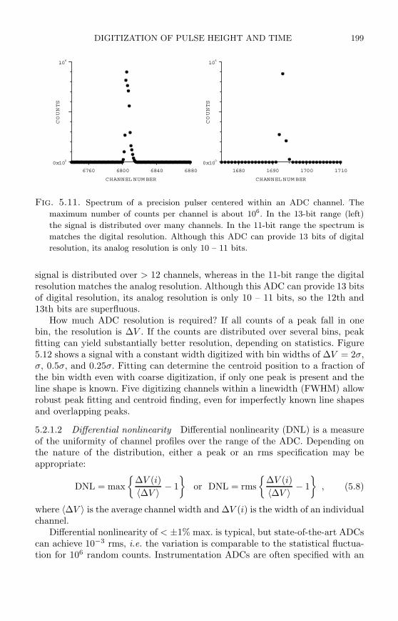
DIGITIZATION OF PULSE HEIGHT AND TIME 199
6760 6800 6840 6880
CHANNEL NUM BER
0x100
106
COUNTS
1680 1690 1700 1710
CHANNEL NUM BER
0x100
106
COUNTS
Fig. 5.11. Spectrum of a precision pulser centered within an ADC channel. The
maximum number of counts per channel is about 106. In the 13-bit range (left)
the signal is distributed over many channels. In the 11-bit range the spectrum is
matches the digital resolution. Although this ADC can provide 13 bits of digital
resolution, its analog resolution is only 10 – 11 bits.
signal is distributed over > 12 channels, whereas in the 11-bit range the digitalresolution matches the analog resolution. Although this ADC can provide 13 bitsof digital resolution, its analog resolution is only 10 – 11 bits, so the 12th and13th bits are superfluous.
How much ADC resolution is required? If all counts of a peak fall in onebin, the resolution is ∆V . If the counts are distributed over several bins, peakfitting can yield substantially better resolution, depending on statistics. Figure5.12 shows a signal with a constant width digitized with bin widths of ∆V = 2σ,σ, 0.5σ, and 0.25σ. Fitting can determine the centroid position to a fraction ofthe bin width even with coarse digitization, if only one peak is present and theline shape is known. Five digitizing channels within a linewidth (FWHM) allowrobust peak fitting and centroid finding, even for imperfectly known line shapesand overlapping peaks.
5.2.1.2 Differential nonlinearity Differential nonlinearity (DNL) is a measureof the uniformity of channel profiles over the range of the ADC. Depending onthe nature of the distribution, either a peak or an rms specification may beappropriate:
DNL = max
∆V (i)
〈∆V 〉 − 1
or DNL = rms
∆V (i)
〈∆V 〉 − 1
, (5.8)
where 〈∆V 〉 is the average channel width and ∆V (i) is the width of an individualchannel.
Differential nonlinearity of < ±1% max. is typical, but state-of-the-art ADCscan achieve 10−3 rms, i.e. the variation is comparable to the statistical fluctua-tion for 106 random counts. Instrumentation ADCs are often specified with an
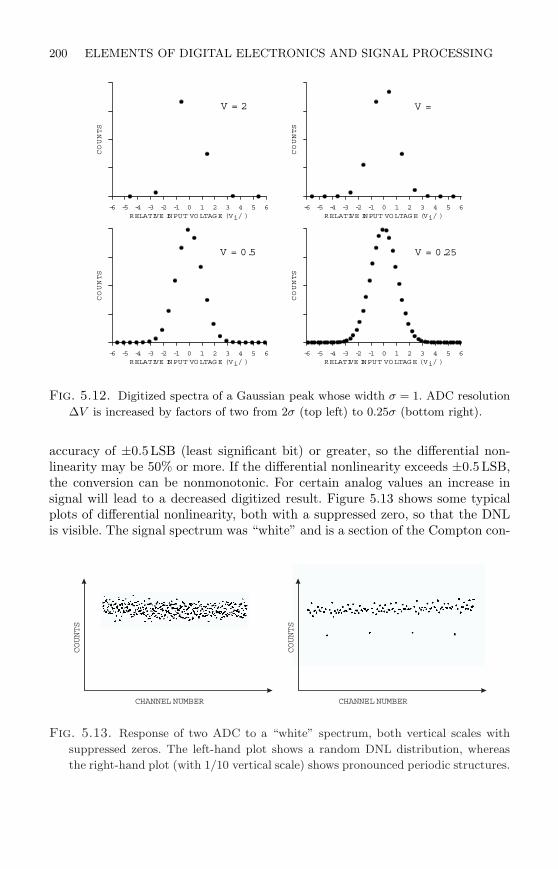
200 ELEMENTS OF DIGITAL ELECTRONICS AND SIGNAL PROCESSING
-6 -5 -4 -3 -2 -1 0 1 2 3 4 5 6RELATIVE INPUT VOLTAGE (Vi/ )
COUNTS
V = 2
-6 -5 -4 -3 -2 -1 0 1 2 3 4 5 6RELATIVE INPUT VOLTAGE (Vi/ )
COUNTS
-6 -5 -4 -3 -2 -1 0 1 2 3 4 5 6RELATIVE INPUT VOLTAGE (Vi/ )
COUNTS
-6 -5 -4 -3 -2 -1 0 1 2 3 4 5 6RELATIVE INPUT VOLTAGE (Vi/ )
COUNTS
V =
V = 0.5 V = 0.25
Fig. 5.12. Digitized spectra of a Gaussian peak whose width σ = 1. ADC resolution
∆V is increased by factors of two from 2σ (top left) to 0.25σ (bottom right).
accuracy of ±0.5LSB (least significant bit) or greater, so the differential non-linearity may be 50% or more. If the differential nonlinearity exceeds ±0.5LSB,the conversion can be nonmonotonic. For certain analog values an increase insignal will lead to a decreased digitized result. Figure 5.13 shows some typicalplots of differential nonlinearity, both with a suppressed zero, so that the DNLis visible. The signal spectrum was “white” and is a section of the Compton con-
CHANNEL NUMBER CHANNEL NUMBER
COUNTS
COUNTS
Fig. 5.13. Response of two ADC to a “white” spectrum, both vertical scales with
suppressed zeros. The left-hand plot shows a random DNL distribution, whereas
the right-hand plot (with 1/10 vertical scale) shows pronounced periodic structures.
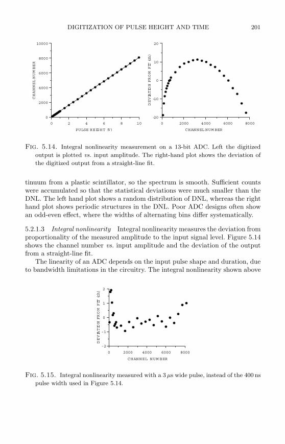
DIGITIZATION OF PULSE HEIGHT AND TIME 201
0 2 4 6 8 10
PULSE HEIGHT (V)
0
2000
4000
6000
8000
10000
CHANNELNUMBER
0 2000 4000 6000 8000
CHANNEL NUM BER
-20
-10
0
10
20
DEVIATIONFROMFIT(ch)
Fig. 5.14. Integral nonlinearity measurement on a 13-bit ADC. Left the digitized
output is plotted vs. input amplitude. The right-hand plot shows the deviation of
the digitized output from a straight-line fit.
tinuum from a plastic scintillator, so the spectrum is smooth. Sufficient countswere accumulated so that the statistical deviations were much smaller than theDNL. The left hand plot shows a random distribution of DNL, whereas the righthand plot shows periodic structures in the DNL. Poor ADC designs often showan odd-even effect, where the widths of alternating bins differ systematically.
5.2.1.3 Integral nonlinearity Integral nonlinearity measures the deviation fromproportionality of the measured amplitude to the input signal level. Figure 5.14shows the channel number vs. input amplitude and the deviation of the outputfrom a straight-line fit.
The linearity of an ADC depends on the input pulse shape and duration, dueto bandwidth limitations in the circuitry. The integral nonlinearity shown above
0 2000 4000 6000 8000
CHANNEL NUM BER
-2
-1
0
1
2
DEVIATIONFROMFIT(ch)
Fig. 5.15. Integral nonlinearity measured with a 3 µs wide pulse, instead of the 400 ns
pulse width used in Figure 5.14.
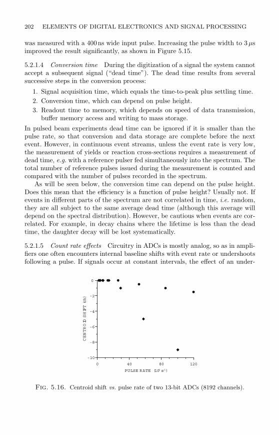
202 ELEMENTS OF DIGITAL ELECTRONICS AND SIGNAL PROCESSING
was measured with a 400ns wide input pulse. Increasing the pulse width to 3µsimproved the result significantly, as shown in Figure 5.15.
5.2.1.4 Conversion time During the digitization of a signal the system cannotaccept a subsequent signal (“dead time”). The dead time results from severalsuccessive steps in the conversion process:
1. Signal acquisition time, which equals the time-to-peak plus settling time.
2. Conversion time, which can depend on pulse height.
3. Readout time to memory, which depends on speed of data transmission,buffer memory access and writing to mass storage.
In pulsed beam experiments dead time can be ignored if it is smaller than thepulse rate, so that conversion and data storage are complete before the nextevent. However, in continuous event streams, unless the event rate is very low,the measurement of yields or reaction cross-sections requires a measurement ofdead time, e.g. with a reference pulser fed simultaneously into the spectrum. Thetotal number of reference pulses issued during the measurement is counted andcompared with the number of pulses recorded in the spectrum.
As will be seen below, the conversion time can depend on the pulse height.Does this mean that the efficiency is a function of pulse height? Usually not. Ifevents in different parts of the spectrum are not correlated in time, i.e. random,they are all subject to the same average dead time (although this average willdepend on the spectral distribution). However, be cautious when events are cor-related. For example, in decay chains where the lifetime is less than the deadtime, the daughter decay will be lost systematically.
5.2.1.5 Count rate effects Circuitry in ADCs is mostly analog, so as in ampli-fiers one often encounters internal baseline shifts with event rate or undershootsfollowing a pulse. If signals occur at constant intervals, the effect of an under-
0 40 80 120
PULSE RATE (103 s-1)
-10
-8
-6
-4
-2
0
CENTROID
SHIFT(ch)
Fig. 5.16. Centroid shift vs. pulse rate of two 13-bit ADCs (8192 channels).
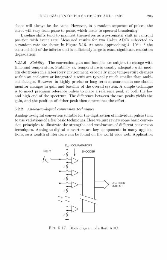
DIGITIZATION OF PULSE HEIGHT AND TIME 203
shoot will always be the same. However, in a random sequence of pulses, theeffect will vary from pulse to pulse, which leads to spectral broadening.
Baseline shifts tend to manifest themselves as a systematic shift in centroidposition with event rate. Measured results for two 13-bit ADCs subjected toa random rate are shown in Figure 5.16. At rates approaching 4 · 104 s−1 thecentroid shift of the inferior unit is sufficiently large to cause significant resolutiondegradation.
5.2.1.6 Stability The conversion gain and baseline are subject to change withtime and temperature. Stability vs. temperature is usually adequate with mod-ern electronics in a laboratory environment, especially since temperature changeswithin an enclosure or integrated circuit are typically much smaller than ambi-ent changes. However, in highly precise or long-term measurements one shouldmonitor changes in gain and baseline of the overall system. A simple techniqueis to inject precision reference pulses to place a reference peak at both the lowand high end of the spectrum. The difference between the two peaks yields thegain, and the position of either peak then determines the offset.
5.2.2 Analog-to-digital conversion techniques
Analog-to-digital converters suitable for the digitization of individual pulses tendto use variations of a few basic techniques. Here we just review some basic conver-sion principles to illustrate the strengths and weaknesses of different conversiontechniques. Analog-to-digital converters are key components in many applica-tions, so a wealth of literature can be found on the world wide web. Application
Vref
R
R
R
R
R
DIGITIZED
OUTPUT
COMPARATORS
ENCODERINPUT
Fig. 5.17. Block diagram of a flash ADC.
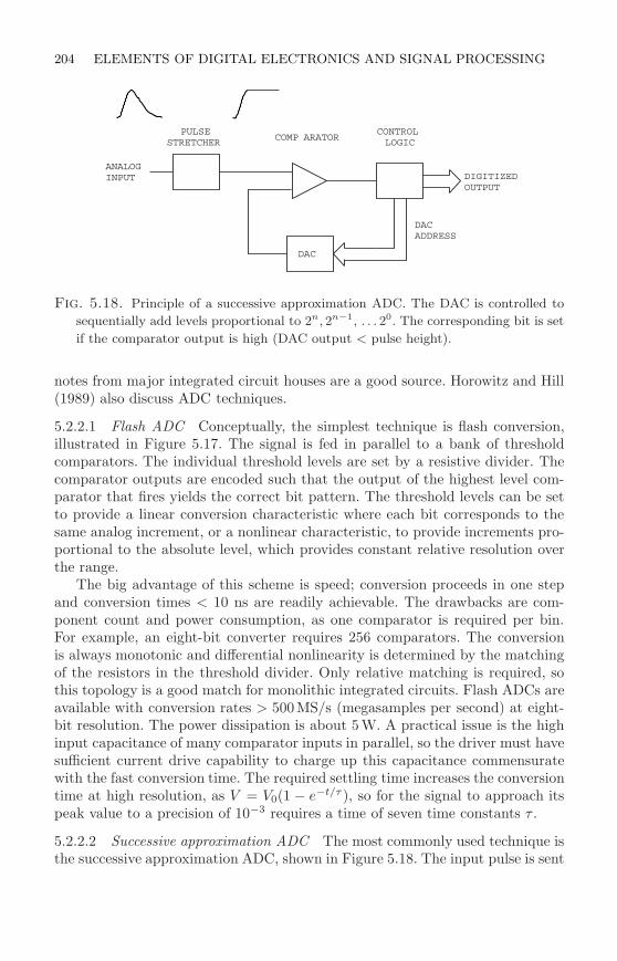
204 ELEMENTS OF DIGITAL ELECTRONICS AND SIGNAL PROCESSING
PULSESTRETCHER
COMP ARATORCONTROLLOGIC
DACADDRESS
DAC
DIGITIZEDOUTPUT
ANALOGINPUT
Fig. 5.18. Principle of a successive approximation ADC. The DAC is controlled to
sequentially add levels proportional to 2n, 2n−1, . . . 20. The corresponding bit is set
if the comparator output is high (DAC output < pulse height).
notes from major integrated circuit houses are a good source. Horowitz and Hill(1989) also discuss ADC techniques.
5.2.2.1 Flash ADC Conceptually, the simplest technique is flash conversion,illustrated in Figure 5.17. The signal is fed in parallel to a bank of thresholdcomparators. The individual threshold levels are set by a resistive divider. Thecomparator outputs are encoded such that the output of the highest level com-parator that fires yields the correct bit pattern. The threshold levels can be setto provide a linear conversion characteristic where each bit corresponds to thesame analog increment, or a nonlinear characteristic, to provide increments pro-portional to the absolute level, which provides constant relative resolution overthe range.
The big advantage of this scheme is speed; conversion proceeds in one stepand conversion times < 10 ns are readily achievable. The drawbacks are com-ponent count and power consumption, as one comparator is required per bin.For example, an eight-bit converter requires 256 comparators. The conversionis always monotonic and differential nonlinearity is determined by the matchingof the resistors in the threshold divider. Only relative matching is required, sothis topology is a good match for monolithic integrated circuits. Flash ADCs areavailable with conversion rates > 500MS/s (megasamples per second) at eight-bit resolution. The power dissipation is about 5 W. A practical issue is the highinput capacitance of many comparator inputs in parallel, so the driver must havesufficient current drive capability to charge up this capacitance commensuratewith the fast conversion time. The required settling time increases the conversiontime at high resolution, as V = V0(1 − e−t/τ ), so for the signal to approach itspeak value to a precision of 10−3 requires a time of seven time constants τ .
5.2.2.2 Successive approximation ADC The most commonly used technique isthe successive approximation ADC, shown in Figure 5.18. The input pulse is sent

DIGITIZATION OF PULSE HEIGHT AND TIME 205
PULSESTRETCHER
COMPARATORCONTROLLOGIC
DACADDRESS
LOAD CORRECTION DATA
SUMMINGAMPLIFIER
DAC
CORR.DAC
RAMV= DNLP-P
DIGITIZEDOUTPUT
ANALOGINPUT
Fig. 5.19. A correction DAC can be used to improve differential nonlinearity.
to a pulse stretcher, which follows the signal until it reaches its cusp and thenholds the peak value. The stretcher output feeds a comparator, whose referenceis provided by a digital-to-analog converter (DAC). The DAC is cycled beginningwith the most significant bits. The corresponding bit is set when the comparatorfires, i.e. the DAC output becomes less than the pulse height. Then the DACcycles through the less significant bits, always setting the corresponding bit whenthe comparator fires. Thus, n-bit resolution requires n steps and yields 2n bins.This technique makes efficient use of circuitry and is fairly fast. High-resolutiondevices (16 – 20 bits) with conversion times of order µs are readily available.Currently, a 16-bit ADC with a conversion time of 1µs (1 MS/s) requires about100mW.
A common limitation is differential nonlinearity, since the resistors that setthe DAC levels must be extremely accurate. For DNL < 1% the resistor de-termining the 212 level in a 13-bit ADC must be accurate to < 2.4 · 10−6. Asa consequence, differential nonlinearity in high-resolution successive approxima-tion converters is typically 10 – 20% and often exceeds the 0.5LSB required toensure monotonic response.
The differential nonlinearity can be corrected by various techniques. One isto average over many channel profiles for a given pulse amplitude, the “slidingscale” technique originated by Gatti (Cottini, Gatti, and Svelto 1963). Here ananalog increment is added event-by-event and the digitized output is correctedaccordingly. Thus, for a large number of events the conversion of a given pulseamplitude utilizes many states of the converter. For a random amplitude dis-tribution this averages over many channel profiles and equalizes the differential
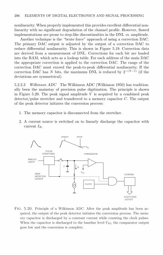
206 ELEMENTS OF DIGITAL ELECTRONICS AND SIGNAL PROCESSING
nonlinearity. When properly implemented this provides excellent differential non-linearity with no significant degradation of the channel profile. However, flawedimplementations are prone to step-like discontinuities in the DNL vs. amplitude.
Another technique is the “brute force” approach of using a correction DAC.The primary DAC output is adjusted by the output of a correction DAC toreduce differential nonlinearity. This is shown in Figure 5.19. Correction dataare derived from a measurement of DNL. Corrections for each bit are loadedinto the RAM, which acts as a lookup table. For each address of the main DACthe appropriate correction is applied to the correction DAC. The range of thecorrection DAC must exceed the peak-to-peak differential nonlinearity. If thecorrection DAC has N bits, the maximum DNL is reduced by 2−(N−1) (if thedeviations are symmetrical).
5.2.2.3 Wilkinson ADC The Wilkinson ADC (Wilkinson 1950) has tradition-ally been the mainstay of precision pulse digitization. The principle is shownin Figure 5.20. The peak signal amplitude V is acquired by a combined peakdetector/pulse stretcher and transferred to a memory capacitor C. The outputof the peak detector initiates the conversion process:
1. The memory capacitor is disconnected from the stretcher.
2. A current source is switched on to linearly discharge the capacitor withcurrent IR.
PULSESTRETCHER COMPARATOR
DIGITIZEDOUTPUT
ANALOGINPUT
START STOP
V
I
V
BL
R
BL
COUNTER
CLOCK
PEAKDETECTOROUTPUT
C
Fig. 5.20. Principle of a Wilkinson ADC. After the peak amplitude has been ac-
quired, the output of the peak detector initiates the conversion process. The mem-
ory capacitor is discharged by a constant current while counting the clock pulses.
When the capacitor is discharged to the baseline level VBL the comparator output
goes low and the conversion is complete.
DIGITIZATION OF PULSE HEIGHT AND TIME 207
3. Simultaneously with commencing the discharge a counter is enabled todetermine the number of clock pulses until the voltage on the capacitorreaches the baseline level VBL.
The time required to discharge the capacitor is a linear function of pulse height,
TC = C · V − VBL
IR, (5.9)
so the counter content provides the digitized pulse height. The clock pulses areprovided by a crystal oscillator, so the time between pulses is extremely uniformand this circuit inherently provides excellent differential linearity. The drawbackis the relatively long conversion time TC , which for a given resolution is propor-tional to the clock period Tclk and the pulse height, TC = n× Tclk (n = channelnumber ∝ pulse height). For example, a clock frequency of 100MHz provides aclock period Tclk = 10ns and a maximum conversion time TC = 82 µs for 13 bits.Clock frequencies of 100MHz are typical, but > 400MHz have been implementedwith excellent performance (DNL < 10−3). This scheme makes efficient use ofcircuitry and allows low power dissipation. Wilkinson ADCs have been imple-mented in 128-channel readout ICs for silicon strip detectors (Garcia-Sciveres etal. 1999). Each ADC added only 100 µm to the length of a channel and a powerof 300 µW per channel (see Chapter 8).
Many important details are not shown in Figure 5.20. For example, the be-ginning of the discharge must be synchronized with the clock. Switching thecurrent source requires some time, which introduces nonlinearity for small sig-nals. Cross-talk from the clock or counter to the analog circuitry can introducecorrelations into the differential nonlinearity, as illustrated in Figure 5.13. It istempting to utilize both the leading and trailing edge of the clock pulse to doublethe clock frequency and reduce conversion time. However, the duty cycle of theclock pulse must be constrained very accurately to 50% to avoid degradation ofdifferential nonlinearity. This technique typically leads to odd–even structures inthe DNL, so the least significant bit can become unusable. Simply suppressingthis bit also reduces the conversion time two-fold, so “clock doubling” becomesself-defeating.
5.2.2.4 Hybrid analog-to-digital converters Conversion techniques can be com-bined to obtain high resolution and short conversion time. One example combinesa flash ADC with a successive approximation or a Wilkinson (ramp run-down)converter. The fast flash ADC provides coarse conversion (e.g. 8 out of 13 bits)and the successive approximation or Wilkinson converter provides fine resolution.Since the second conversion range is small, the conversion time is significantlyreduced. For example, a Wilkinson ADC covering 256 channels with a 100MHzclock requires only 2.6µs, which is comparable to a successive approximationADC, but with superior differential nonlinearity.
Another approach is to use flash ADCs with sub-ranging. Not all applicationsrequire constant absolute resolution over the full range. Sometimes only relative
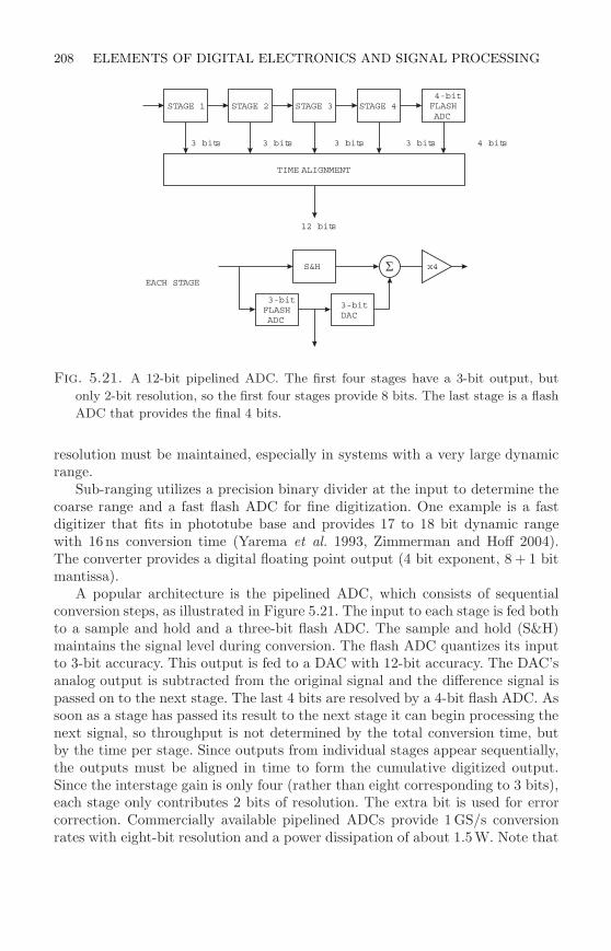
208 ELEMENTS OF DIGITAL ELECTRONICS AND SIGNAL PROCESSING
STAGE 1 STAGE 2 STAGE 3 STAGE 4
TIME ALIGNMENT
4-bitFLASHADC
3-bitFLASHADC
3-bitDAC
x4S&H EACH STAGE
3 bits 3 bits 3 bits 3 bits 4 bits
12 bits
Fig. 5.21. A 12-bit pipelined ADC. The first four stages have a 3-bit output, but
only 2-bit resolution, so the first four stages provide 8 bits. The last stage is a flash
ADC that provides the final 4 bits.
resolution must be maintained, especially in systems with a very large dynamicrange.
Sub-ranging utilizes a precision binary divider at the input to determine thecoarse range and a fast flash ADC for fine digitization. One example is a fastdigitizer that fits in phototube base and provides 17 to 18 bit dynamic rangewith 16ns conversion time (Yarema et al. 1993, Zimmerman and Hoff 2004).The converter provides a digital floating point output (4 bit exponent, 8 + 1 bitmantissa).
A popular architecture is the pipelined ADC, which consists of sequentialconversion steps, as illustrated in Figure 5.21. The input to each stage is fed bothto a sample and hold and a three-bit flash ADC. The sample and hold (S&H)maintains the signal level during conversion. The flash ADC quantizes its inputto 3-bit accuracy. This output is fed to a DAC with 12-bit accuracy. The DAC’sanalog output is subtracted from the original signal and the difference signal ispassed on to the next stage. The last 4 bits are resolved by a 4-bit flash ADC. Assoon as a stage has passed its result to the next stage it can begin processing thenext signal, so throughput is not determined by the total conversion time, butby the time per stage. Since outputs from individual stages appear sequentially,the outputs must be aligned in time to form the cumulative digitized output.Since the interstage gain is only four (rather than eight corresponding to 3 bits),each stage only contributes 2 bits of resolution. The extra bit is used for errorcorrection. Commercially available pipelined ADCs provide 1 GS/s conversionrates with eight-bit resolution and a power dissipation of about 1.5W. Note that
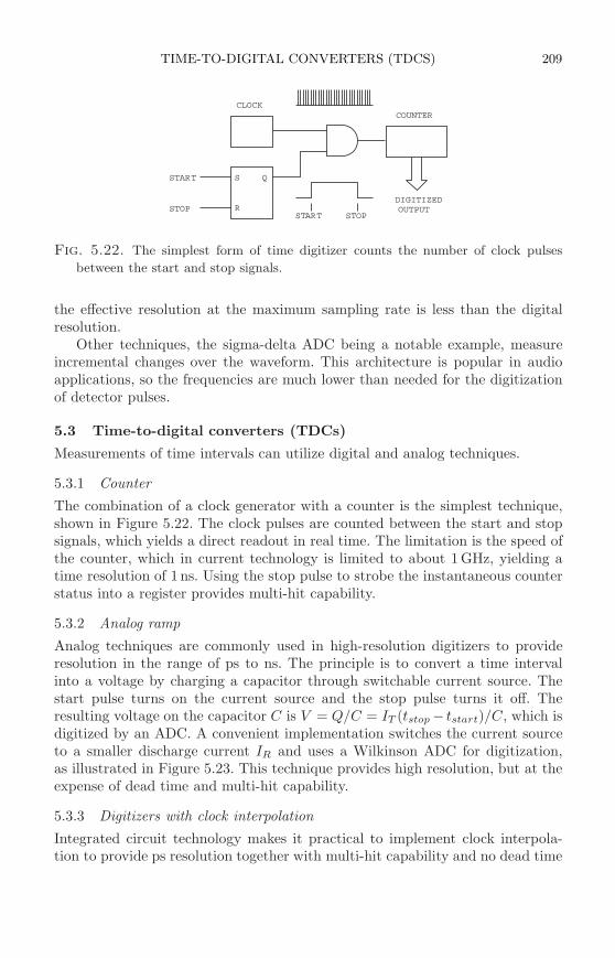
TIME-TO-DIGITAL CONVERTERS (TDCS) 209
DIGITIZEDOUTPUT
COUNTERCLOCK
QSSTART
STOP RSTART STOP
Fig. 5.22. The simplest form of time digitizer counts the number of clock pulses
between the start and stop signals.
the effective resolution at the maximum sampling rate is less than the digitalresolution.
Other techniques, the sigma-delta ADC being a notable example, measureincremental changes over the waveform. This architecture is popular in audioapplications, so the frequencies are much lower than needed for the digitizationof detector pulses.
5.3 Time-to-digital converters (TDCs)
Measurements of time intervals can utilize digital and analog techniques.
5.3.1 Counter
The combination of a clock generator with a counter is the simplest technique,shown in Figure 5.22. The clock pulses are counted between the start and stopsignals, which yields a direct readout in real time. The limitation is the speed ofthe counter, which in current technology is limited to about 1 GHz, yielding atime resolution of 1 ns. Using the stop pulse to strobe the instantaneous counterstatus into a register provides multi-hit capability.
5.3.2 Analog ramp
Analog techniques are commonly used in high-resolution digitizers to provideresolution in the range of ps to ns. The principle is to convert a time intervalinto a voltage by charging a capacitor through switchable current source. Thestart pulse turns on the current source and the stop pulse turns it off. Theresulting voltage on the capacitor C is V = Q/C = IT (tstop − tstart)/C, which isdigitized by an ADC. A convenient implementation switches the current sourceto a smaller discharge current IR and uses a Wilkinson ADC for digitization,as illustrated in Figure 5.23. This technique provides high resolution, but at theexpense of dead time and multi-hit capability.
5.3.3 Digitizers with clock interpolation
Integrated circuit technology makes it practical to implement clock interpola-tion to provide ps resolution together with multi-hit capability and no dead time
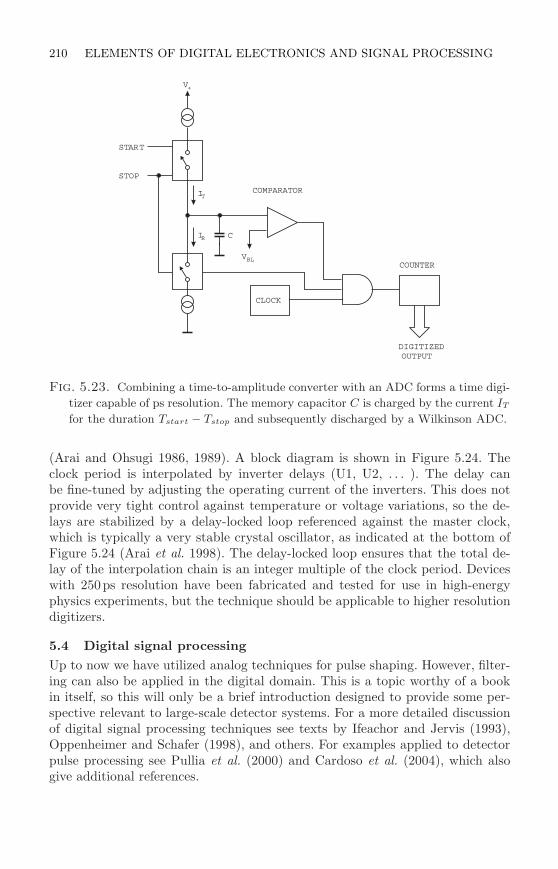
210 ELEMENTS OF DIGITAL ELECTRONICS AND SIGNAL PROCESSING
COMPARATOR
DIGITIZEDOUTPUT
V
I
I
V
BL
R
T
+
COUNTER
CLOCK
START
STOP
C
Fig. 5.23. Combining a time-to-amplitude converter with an ADC forms a time digi-
tizer capable of ps resolution. The memory capacitor C is charged by the current IT
for the duration Tstart − Tstop and subsequently discharged by a Wilkinson ADC.
(Arai and Ohsugi 1986, 1989). A block diagram is shown in Figure 5.24. Theclock period is interpolated by inverter delays (U1, U2, . . . ). The delay canbe fine-tuned by adjusting the operating current of the inverters. This does notprovide very tight control against temperature or voltage variations, so the de-lays are stabilized by a delay-locked loop referenced against the master clock,which is typically a very stable crystal oscillator, as indicated at the bottom ofFigure 5.24 (Arai et al. 1998). The delay-locked loop ensures that the total de-lay of the interpolation chain is an integer multiple of the clock period. Deviceswith 250ps resolution have been fabricated and tested for use in high-energyphysics experiments, but the technique should be applicable to higher resolutiondigitizers.
5.4 Digital signal processing
Up to now we have utilized analog techniques for pulse shaping. However, filter-ing can also be applied in the digital domain. This is a topic worthy of a bookin itself, so this will only be a brief introduction designed to provide some per-spective relevant to large-scale detector systems. For a more detailed discussionof digital signal processing techniques see texts by Ifeachor and Jervis (1993),Oppenheimer and Schafer (1998), and others. For examples applied to detectorpulse processing see Pullia et al. (2000) and Cardoso et al. (2004), which alsogive additional references.
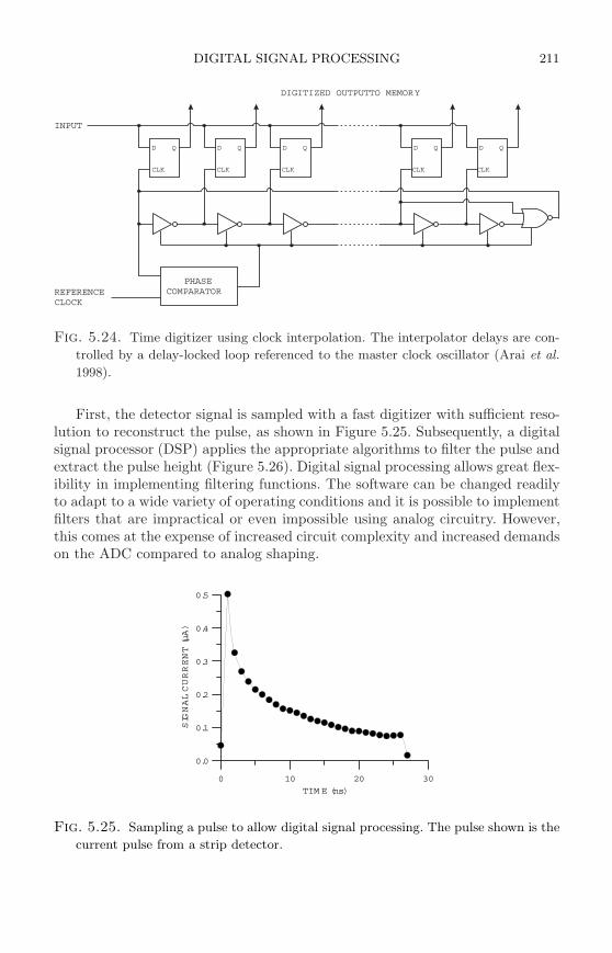
DIGITAL SIGNAL PROCESSING 211
D D D D D
CLK CLK CLK CLK CLK
Q Q Q Q Q
PHASECOMPARATOR
INPUT
REFERENCECLOCK
DIGITIZED OUTPUTTO MEMORY
Fig. 5.24. Time digitizer using clock interpolation. The interpolator delays are con-
trolled by a delay-locked loop referenced to the master clock oscillator (Arai et al.
1998).
First, the detector signal is sampled with a fast digitizer with sufficient reso-lution to reconstruct the pulse, as shown in Figure 5.25. Subsequently, a digitalsignal processor (DSP) applies the appropriate algorithms to filter the pulse andextract the pulse height (Figure 5.26). Digital signal processing allows great flex-ibility in implementing filtering functions. The software can be changed readilyto adapt to a wide variety of operating conditions and it is possible to implementfilters that are impractical or even impossible using analog circuitry. However,this comes at the expense of increased circuit complexity and increased demandson the ADC compared to analog shaping.
0 10 20 30
TIM E (ns)
0.0
0.1
0.2
0.3
0.4
0.5
SIGNALCURRENT(µA)
Fig. 5.25. Sampling a pulse to allow digital signal processing. The pulse shown is the
current pulse from a strip detector.
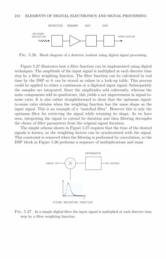
212 ELEMENTS OF DIGITAL ELECTRONICS AND SIGNAL PROCESSING
INCIDENTRADIATION PUBLICATION
DETECTOR PREAMP ADC DSP
Fig. 5.26. Block diagram of a detector readout using digital signal processing.
Figure 5.27 illustrates how a filter function can be implemented using digitaltechniques. The amplitude of the input signal is multiplied at each discrete timestep by a filter weighting function. The filter function can be calculated in realtime by the DSP or it can be stored as values in a look-up table. This processcould be applied to either a continuous or a digitized input signal. Subsequentlythe samples are integrated. Since the amplitudes add coherently, whereas thenoise components add in quadrature, this yields a net improvement in signal-to-noise ratio. It is also rather straightforward to show that the optimum signal-to-noise ratio obtains when the weighting function has the same shape as theinput signal. This is an example of a “matched filter”. However this is only theoptimum filter for retrieving the signal while retaining its shape. As we haveseen, integrating the signal to extend its duration and then filtering decouplesthe choice of filter parameters from the original signal duration.
The simple scheme shown in Figure 5.27 requires that the time of the desiredsignals is known, so the weighting factors can be synchronized with the signal.This constraint is removed when the filtering is performed by convolution, so theDSP block in Figure 5.26 performs a sequence of multiplications and sums
t
FILTER WEIGHTING FUNCTION
INTEGRATOR
INPUT OUTPUT
Fig. 5.27. In a simple digital filter the input signal is multiplied at each discrete time
step by a filter weighting function.
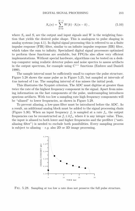
DIGITAL SIGNAL PROCESSING 213
So(n) =
N−1∑
k=0
W (k) · Si(n − k) , (5.10)
where So and Si are the output and input signals and W is the weighting func-tion that yields the desired pulse shape. This is analogous to pulse shaping inanalog systems (eqn 4.1). In digital signal processing this is referred to as a finiteimpulse response (FIR) filter, similar to an infinite impulse response (IIR) filter,which takes the sum to infinity. Specialized digital signal processors optimizedto perform these functions are available, but FPGAs also allow very efficientimplementations. Without special hardware, algorithms can be tested on a desk-top computer using realistic detector pulses and noise spectra to assess artifactsin the output spectrum, for example using C++ functions (Embree and Danieli1999).
The sample interval must be sufficiently small to capture the pulse structure.Figure 5.28 shows the same pulse as in Figure 5.25, but sampled at intervals of4 ns instead of 1 ns. The sampling interval of 4 ns misses the initial peak.
This illustrates the Nyquist criterion. The ADC must digitize at greater thantwice the rate of the highest frequency component in the signal. Apart from miss-ing information on the fast components of the pulse, undersampling introducesspurious artifacts. With too low a sampling rate high frequency components willbe “aliased” to lower frequencies, as shown in Figure 5.29.
To prevent aliasing, a low-pass filter must be introduced before the ADC. Asa result, an additional analog block must be added to the signal processing chain(Figure 5.30). When an input frequency fi is sampled at a rate fs, the outputfrequencies can be reconstructed as fi ± kfs, where k is any integer value. Thus,the input is aliased to both lower and higher frequencies and the prefilter (“anti-aliasing filter”) is needed to exclude both possibilities. Every sampling processis subject to aliasing – e.g. also 2D or 3D image processing.
0 10 20 30
TIM E (ns)
0.0
0.1
0.2
0.3
0.4
0.5
SIGNALCURRENT(µA)
Fig. 5.28. Sampling at too low a rate does not preserve the full pulse structure.
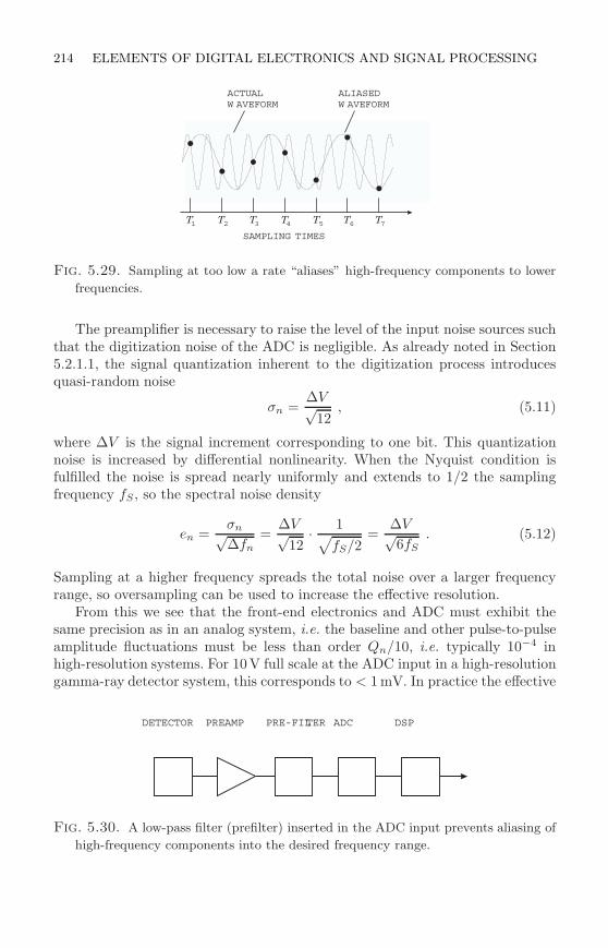
214 ELEMENTS OF DIGITAL ELECTRONICS AND SIGNAL PROCESSING
SAMPLING TIMES
T T T T T T T1 2 3 4 5 6 7
ACTUALW AVEFORM
ALIASEDW AVEFORM
Fig. 5.29. Sampling at too low a rate “aliases” high-frequency components to lower
frequencies.
The preamplifier is necessary to raise the level of the input noise sources suchthat the digitization noise of the ADC is negligible. As already noted in Section5.2.1.1, the signal quantization inherent to the digitization process introducesquasi-random noise
σn =∆V√
12, (5.11)
where ∆V is the signal increment corresponding to one bit. This quantizationnoise is increased by differential nonlinearity. When the Nyquist condition isfulfilled the noise is spread nearly uniformly and extends to 1/2 the samplingfrequency fS, so the spectral noise density
en =σn√∆fn
=∆V√
12· 1√
fS/2=
∆V√6fS
. (5.12)
Sampling at a higher frequency spreads the total noise over a larger frequencyrange, so oversampling can be used to increase the effective resolution.
From this we see that the front-end electronics and ADC must exhibit thesame precision as in an analog system, i.e. the baseline and other pulse-to-pulseamplitude fluctuations must be less than order Qn/10, i.e. typically 10−4 inhigh-resolution systems. For 10V full scale at the ADC input in a high-resolutiongamma-ray detector system, this corresponds to < 1 mV. In practice the effective
DETECTOR PREAMP ADC DSPPRE-FILTER
Fig. 5.30. A low-pass filter (prefilter) inserted in the ADC input prevents aliasing of
high-frequency components into the desired frequency range.
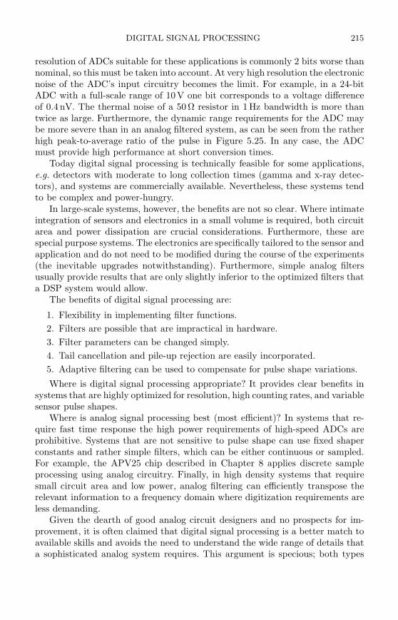
DIGITAL SIGNAL PROCESSING 215
resolution of ADCs suitable for these applications is commonly 2 bits worse thannominal, so this must be taken into account. At very high resolution the electronicnoise of the ADC’s input circuitry becomes the limit. For example, in a 24-bitADC with a full-scale range of 10V one bit corresponds to a voltage differenceof 0.4 nV. The thermal noise of a 50Ω resistor in 1Hz bandwidth is more thantwice as large. Furthermore, the dynamic range requirements for the ADC maybe more severe than in an analog filtered system, as can be seen from the ratherhigh peak-to-average ratio of the pulse in Figure 5.25. In any case, the ADCmust provide high performance at short conversion times.
Today digital signal processing is technically feasible for some applications,e.g. detectors with moderate to long collection times (gamma and x-ray detec-tors), and systems are commercially available. Nevertheless, these systems tendto be complex and power-hungry.
In large-scale systems, however, the benefits are not so clear. Where intimateintegration of sensors and electronics in a small volume is required, both circuitarea and power dissipation are crucial considerations. Furthermore, these arespecial purpose systems. The electronics are specifically tailored to the sensor andapplication and do not need to be modified during the course of the experiments(the inevitable upgrades notwithstanding). Furthermore, simple analog filtersusually provide results that are only slightly inferior to the optimized filters thata DSP system would allow.
The benefits of digital signal processing are:
1. Flexibility in implementing filter functions.
2. Filters are possible that are impractical in hardware.
3. Filter parameters can be changed simply.
4. Tail cancellation and pile-up rejection are easily incorporated.
5. Adaptive filtering can be used to compensate for pulse shape variations.
Where is digital signal processing appropriate? It provides clear benefits insystems that are highly optimized for resolution, high counting rates, and variablesensor pulse shapes.
Where is analog signal processing best (most efficient)? In systems that re-quire fast time response the high power requirements of high-speed ADCs areprohibitive. Systems that are not sensitive to pulse shape can use fixed shaperconstants and rather simple filters, which can be either continuous or sampled.For example, the APV25 chip described in Chapter 8 applies discrete sampleprocessing using analog circuitry. Finally, in high density systems that requiresmall circuit area and low power, analog filtering can efficiently transpose therelevant information to a frequency domain where digitization requirements areless demanding.
Given the dearth of good analog circuit designers and no prospects for im-provement, it is often claimed that digital signal processing is a better match toavailable skills and avoids the need to understand the wide range of details thata sophisticated analog system requires. This argument is specious; both types
216 ELEMENTS OF DIGITAL ELECTRONICS AND SIGNAL PROCESSING
of systems require careful analog design. Nevertheless, progress in fast ADCs(precision, reduced power) will expand the range of DSP applications.
References
Arai, Y. and Ohsugi, T. (1986). An idea of deadtimeless readout system by usingtime memory cell. Proceedings of the 1986 Summer Study on the Physics ofthe Superconducting Super Collider pp. 455–457
Arai, Y. and Ohsugi, T. (1989). TMC – a CMOS time to digital converter VLSI.IEEE Trans. Nucl. Sci. NS-36/1 (1989) 528–531
Arai, Y. et al. (1998). Time memory cell VLSI for the PHENIX drift chamber.IEEE Trans. Nucl. Sci. NS-45/3 (1998) 735 – 739 and references therein.
Cardoso, J.M. et al. (2004). A high performance hardware reconfigurable hard-ware platform for digital pulse processing. IEEE Trans. Nucl. Sci. NS-51/3(2004) 921–925
Cottini, C., Gatti, E., and Svelto, V. (1963). A new method for analog-to-digitalconversion. Nucl. Instr. Meth. 24 (1963) 241–242
Embree, P.M. and Danieli, D. (1999). C++ Algorithms for Digital Signal Pro-cessing. Prentice Hall PTR, Upper Saddle River. ISBN 0-13-179144-3,TK5102.9 E45
Garcia-Sciveres, M. et al. (1999). The SVX3D integrated circuit for dead-timeless silicon strip readout. Nucl. Instr. Meth. A435 (1999) 58–64
Horowitz, P. and Hill, W. (1989). The Art of Electronics. Cambridge UniversityPress, 2nd edition, ISBN 0-5213-7095-7
Ifeachor, E.C. and Jervis, B.W. (1993). Digital Signal Processing – A PracticalApproach. Addison-Wesley, Wokingham. ISBN 0-201-54413-X, TK5102.I33
Oppenheimer, A.V. and Schafer, R.W. (1998). Discrete-Time Signal Processing.Prentice Hall, Upper Saddle River. ISBN 0-13-754920-2, TK5102.9.067
Pullia, A. et al. (2000). Quasi-optimum γ and x spectroscopy based on real-timedigital techniques. Nucl. Instr. Meth. A439 (2000) 378–384
Shannon, C.E. (1949). Communication in the presence of noise. Proc. IRE 37/1(1949) 10–21, reprinted in Proc. IEEE 86/2 (1998) 447–457
Wilkinson, D.H. (1950). A stable ninety-nine channel pulse amplitude analyserfor slow counting. Proc. Cambridge Phil. Soc. 46/3 (1950) 508–518
Yarema, R.J. et al. (1993). Wide range charge integrator and encoder ASIC forphotomultiplier tubes. IEEE Trans. Nucl. Sci. NS-40/4 (1993) 750–752
Zimmerman, T. and Hoff, J.R. (2004). The design of a charge-integrating mod-ified floating-point ADC chip. IEEE J. Solid-State Circuits SC-39/6 (2004)895–905
6
TRANSISTORS AND AMPLIFIERS
As shown in Chapter 3 the electronic noise of a well-designed amplifier chainis determined by the first amplifying stage. Taking this a step further, in awell-designed amplifier stage, the noise is dominated by the input amplifyingdevice, e.g. a bipolar transistor, a junction field effect transistor (JFET), ormetal-oxide-semiconductor field effect transistor (MOSFET). At a basic level,one can consider individual amplifying devices as amplifiers, so the first stagemust amplify its inherent noise to a level that overrides the noise of subsequentdevices and other components. Understanding the noise of amplifying devicesand its optimization requires some knowledge of device physics, so this chapterfirst describes the basic principles of bipolar and field effect transistors and howthese devices are used in simple amplifiers. We then analyze the noise propertiesof FETs and bipolar transistors and turn to some illustrative amplifier designsthat show how the various types of devices can be used effectively.
This chapter presents only an overview. The following books are recom-mended to those who wish to delve deeper. The texts by Shockley (1950) andGrove (1967) may appear dated, but they give excellent treatments of the basicphysics. Sze (1981, 2002) provides a comprehensive overview of practically allsemiconductor devices. Taur and Ning (1998) and Takeda, Yang, and Miura-Hamada (1995) give a more modern perspective relevant to modern integratedcircuits. Tsividis (1987) covers MOS transistors in great detail. Baker, Li, andBoyce (1998) cover simulation and layout of integrated circuits. Wolf (1995, 2002)provides a detailed and quite up-to-date discussion of submicron integrated cir-cuits. Clearly, this is not an exhaustive list and also reflects some personal pro-clivities (the primary sources often give the clearest explanations).
6.1 Bipolar transistors
Although the first patent awarded for a semiconductor amplifier described a fieldeffect transistor, the first practical devices were bipolar transistors. The firstbipolar transistors were point-contact transistors (Bardeen and Brattain 1948),which proved to be an evolutionary dead-end. All modern bipolar transistors arejunction transistors (Shockley 1949), which fully exploit the presence of bothmajority and minority carriers. The principle is illustrated in the npn structureshown in Figure 6.1. The following explanation applies the signal to the base,which separates the input and output currents, but differs from many textbooksthat apply the signal to the emitter. This has historical reasons, as the firsttransistors had poor current gain and frequency response, so applying the signalto the emitter was advantageous. This constraint was overcome decades ago and
217
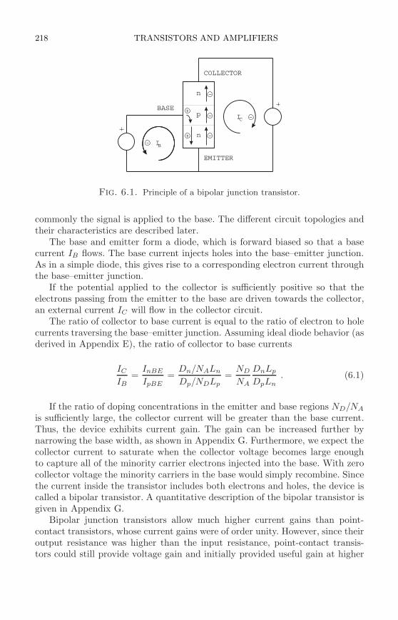
218 TRANSISTORS AND AMPLIFIERS
n
p
nIB
IC
BASE
COLLECTOR
EMITTER
Fig. 6.1. Principle of a bipolar junction transistor.
commonly the signal is applied to the base. The different circuit topologies andtheir characteristics are described later.
The base and emitter form a diode, which is forward biased so that a basecurrent IB flows. The base current injects holes into the base–emitter junction.As in a simple diode, this gives rise to a corresponding electron current throughthe base–emitter junction.
If the potential applied to the collector is sufficiently positive so that theelectrons passing from the emitter to the base are driven towards the collector,an external current IC will flow in the collector circuit.
The ratio of collector to base current is equal to the ratio of electron to holecurrents traversing the base–emitter junction. Assuming ideal diode behavior (asderived in Appendix E), the ratio of collector to base currents
IC
IB=
InBE
IpBE=
Dn/NALn
Dp/NDLp=
ND
NA
DnLp
DpLn. (6.1)
If the ratio of doping concentrations in the emitter and base regions ND/NA
is sufficiently large, the collector current will be greater than the base current.Thus, the device exhibits current gain. The gain can be increased further bynarrowing the base width, as shown in Appendix G. Furthermore, we expect thecollector current to saturate when the collector voltage becomes large enoughto capture all of the minority carrier electrons injected into the base. With zerocollector voltage the minority carriers in the base would simply recombine. Sincethe current inside the transistor includes both electrons and holes, the device iscalled a bipolar transistor. A quantitative description of the bipolar transistor isgiven in Appendix G.
Bipolar junction transistors allow much higher current gains than point-contact transistors, whose current gains were of order unity. However, since theiroutput resistance was higher than the input resistance, point-contact transis-tors could still provide voltage gain and initially provided useful gain at higher
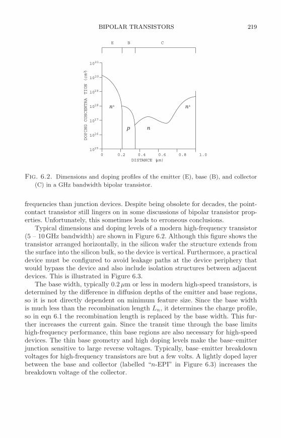
BIPOLAR TRANSISTORS 219
10
10
10
10
10
10
10
15
16
17
18
19
20
21
0 0.2 0.4 0.6 0.8 1.0
DOPING
CONCENTRA
TION
(cm)
-3
DISTANCE ( m)
E B
nn ++
C
p n
Fig. 6.2. Dimensions and doping profiles of the emitter (E), base (B), and collector
(C) in a GHz bandwidth bipolar transistor.
frequencies than junction devices. Despite being obsolete for decades, the point-contact transistor still lingers on in some discussions of bipolar transistor prop-erties. Unfortunately, this sometimes leads to erroneous conclusions.
Typical dimensions and doping levels of a modern high-frequency transistor(5 – 10GHz bandwidth) are shown in Figure 6.2. Although this figure shows thetransistor arranged horizontally, in the silicon wafer the structure extends fromthe surface into the silicon bulk, so the device is vertical. Furthermore, a practicaldevice must be configured to avoid leakage paths at the device periphery thatwould bypass the device and also include isolation structures between adjacentdevices. This is illustrated in Figure 6.3.
The base width, typically 0.2 µm or less in modern high-speed transistors, isdetermined by the difference in diffusion depths of the emitter and base regions,so it is not directly dependent on minimum feature size. Since the base widthis much less than the recombination length Ln, it determines the charge profile,so in eqn 6.1 the recombination length is replaced by the base width. This fur-ther increases the current gain. Since the transit time through the base limitshigh-frequency performance, thin base regions are also necessary for high-speeddevices. The thin base geometry and high doping levels make the base–emitterjunction sensitive to large reverse voltages. Typically, base–emitter breakdownvoltages for high-frequency transistors are but a few volts. A lightly doped layerbetween the base and collector (labelled “n-EPI” in Figure 6.3) increases thebreakdown voltage of the collector.
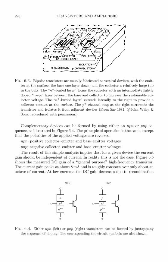
220 TRANSISTORS AND AMPLIFIERS
Fig. 6.3. Bipolar transistors are usually fabricated as vertical devices, with the emit-
ter at the surface, the base one layer down, and the collector a relatively large tub
in the bulk. The “n+-buried layer” forms the collector with an intermediate lightly
doped “n-epi” layer between the base and collector to increase the sustainable col-
lector voltage. The “n+-buried layer” extends laterally to the right to provide a
collector contact at the surface. The p+ channel stop at the right surrounds the
transistor and isolates it from adjacent devices (From Sze 1981. c©John Wiley &
Sons, reproduced with permission.)
Complementary devices can be formed by using either an npn or pnp se-quence, as illustrated in Figure 6.4. The principle of operation is the same, exceptthat the polarities of the applied voltages are reversed.
npn: positive collector–emitter and base–emitter voltages.
pnp: negative collector–emitter and base–emitter voltages.
The result of this simple analysis implies that for a given device the currentgain should be independent of current. In reality this is not the case. Figure 6.5shows the measured DC gain of a “general purpose” high-frequency transistor.The current gain peaks at about 8 mA and is roughly constant over only about anoctave of current. At low currents the DC gain decreases due to recombination
n p
p n
n p++ ++
+ +
E E
B B
C C
NPN PNP
Fig. 6.4. Either npn (left) or pnp (right) transistors can be formed by juxtaposing
the sequence of doping. The corresponding the circuit symbols are also shown.
BIPOLAR TRANSISTORS 221
0.1 1 10 100COLLECTOR CURRENT (mA)
0
50
100
150
200
250
DCCURRENTGAIN
Fig. 6.5. Direct current gain vs. collector current of a “general purpose” high fre-
quency transistor.
in the base–emitter depletion region. We’ll return to this phenomenon in thenext chapter when discussing radiation effects. At high currents the current gaindrops because of resistive voltage losses, shifting of the high field region at thecollector (increased base width), and loss of injection efficiency as the carrierdensity approaches the doping concentration, depending on the specific design.
For low-power applications the behavior at low currents is important. The“ideal” DC gain depends only on device and material constants, whereas the re-combination depends on the local density of injected electrons and holes relativeto the concentration of recombination centers. Thus, the relative degradation ofDC gain due to recombination depends on the current density. Within the samefabrication process and at a given operating current, a large transistor will ex-
10-5
10-4
10-3
10-2
10-1
100
101
102
103
EM ITTER CURRENT DENSITY (µA/µm 2)
0
20
40
60
80
100
DCCURRENTGAIN
NPN
10-5
10-4
10-3
10-2
10-1
100
101
102
103
EM ITTER CURRENT DENSITY (µA/µm 2)
0
10
20
30
40
50
DCCURRENTGAIN
PNP
Fig. 6.6. DC gain vs. emitter current density of npn and pnp devices fabricated in a
modern bipolar transistor integrated circuit process. The emitter area is 45 (µm)2,
so to obtain the total emitter current the current density must be multiplied by 45.
222 TRANSISTORS AND AMPLIFIERS
hibit more recombination than a small transistor. Stated differently, for a givencurrent, the large transistor will offer more recombination centers for the samenumber of carriers. As shown in Figure 6.6 modern devices exhibit DC gain thatis quite uniform over orders of magnitude of emitter current and extending downto currents at the µA level.
The frequency response of the current gain is similar to that of the simpleamplifier discussed in Chapter 2. At low frequencies the current gain is constant(= βDC) and then drops off linearly with frequency. In the high frequency regime
β = −ifT
f, (6.2)
where fT is the frequency where the extrapolated current gain equals one. Thisis called the transit frequency. The gain–bandwidth product is constant, so thecutoff frequency, where the current gain rolls off by 1/
√2,
fβ =fT
βDC. (6.3)
In a transistor with fT = 5 GHz and a low-frequency current gain of 100 thecurrent gain remains roughly constant up to 50 MHz and then falls off inverselyproportional to frequency with a 90 phase shift.
6.1.1 Bipolar transistors in amplifiers
To form amplifiers transistors can be connected in three basic configurations,common-emitter, common-base, and common-collector, which will be describedbelow. The three configurations have different properties, which complement eachother. All three are frequently combined to obtain the desired characteristics ofthe overall amplifier.
The differential behavior, as for a small signal superimposed on the bias volt-ages, is the same for both npn and pnp devices, so the basic amplifier equationsapply to both types. The availability of complementary transistors offers greatflexibility in circuit design and also provides greater gain and bandwidth thanpure npn or pnp designs. Figure 6.4 shows npn and pnp transistors together withtheir respective circuit symbols.
6.1.1.1 Common-emitter amplifier In a common-emitter amplifier the emitteris common to both the input and output. Figure 6.7 shows a common-emitteramplifier and its equivalent circuit.
The input signal is applied to the base, the output taken from the collector.The change in collector current ∆IC in response to a base current ∆IB is ∆IC =β∆IB , so the change in output voltage ∆VC = ∆ICRL = β∆IBRL, whereRL = RRC/R + RC is the parallel combination of RC and the external loadR. Note that we must distinguish between the DC gain βDC = IC/IB and thedifferential current gain β = dIC/dIB , which applies to small signal variationssuperimposed on the DC bias.
BIPOLAR TRANSISTORS 223
V V+ +
SOURCE LOAD
R
R R
R R
I
R
V
V Q Q
V
V
C
C C
0
C
C1
B1 1 2
C2
B2
Fig. 6.7. Common-emitter amplifier with its equivalent circuit (left). Note that the
effective load resistance is the parallel combination of R and RC . The second panel
shows a variant of the common-emitter amplifier configured as a differential pair.
Although the bipolar transistor is a current driven device, it is often con-venient to consider its response to input voltage. Consider a transistor in thecommon-emitter configuration. The voltage gain
Av =dVout
dVin=
dIC
dVBERL = gmRL . (6.4)
Since the dependence of base current on base–emitter voltage is given by thediode equation
IB = IR(eeVBE/kT − 1) ≈ IReeVBE/kT , (6.5)
the resulting collector current is
IC = βDCIB = βDCIReeVBE/kT (6.6)
and the transconductance, i.e. the change in collector current vs. base–emittervoltage
gm ≡ dIC
dVBE= βDCIR
e
kTeeVBE/kT =
e
kTIC . (6.7)
At a given temperature the transconductance depends only on collector current,so for any bipolar transistor – regardless of its internal design, whether “antique”or futuristic and regardless of the material, whether Si, Ge, SiGe or any otherheterojunction – setting the collector current determines the transconductance.Since at room temperature kT/e = 26 mV,
gm =IC
0.026 [mV]≈ 40
[
V−1]
IC . (6.8)

224 TRANSISTORS AND AMPLIFIERS
We can also interpret this result in the following manner. Because of the emitterdiode’s current–voltage characteristic, for small current excursions it behaves asa resistance
rE =dVBE
dIE=
kT
eIE. (6.9)
Since IE ≈ IC , the transconductance gm ≈ 1/rE .Thus is not quite true, as the doped channel connecting the physical emit-
ter to the external connection has some resistance, so the emitter resistance isthe sum of the dynamic resistance rE and the parasitic connection resistance.However, at low currents the parasitic resistance is usually negligible, so in smallsignal amplifiers the voltage gain is of a bipolar transistor is well-controlled bythe emitter current and load resistance.
A variant of the common-emitter amplifier is the differential pair (sometimescalled a “long tailed pair”), also shown in Figure 6.7. Both emitters are connectedtogether to a current source I0, so the total current is fixed. The quiescent currentin each transistor is I0/2, so the transconductance
gm1 = gm2 =e
kT· I0
2. (6.10)
A small change in the input voltage to the first transistor VB1 + ∆V changes itscollector current by
∆IC1 = ∆V gm1 =∆V
2· e
kT· I0
2. (6.11)
Only half of the signal voltage is applied to each transistor, as the input dividesequally between the two base–emitter junctions. Since the total current is fixed,the current of the second transistor Q2 must decrease by the same amount,∆IC2 = −∆IC1. Viewed in terms of emitter voltage, increasing VB1 pulls up thevoltage at the common-emitter connection, so the base–emitter voltage of thesecond transistor is reduced and its current decreases. The collector voltages
VC1 = V+ −[
I0
2+ ∆V · e
kT· I0
4
]
· RC
VC2 = V+ −[
I0
2− ∆V · e
kT· I0
4
]
· RC , (6.12)
so the change in output voltage
VC1 − VC2 = ∆V · e
kT· I0
2. (6.13)
The differential voltage gain is half of a single transistor operating at the col-lector current I0. However, the differential configuration has an important ad-vantage, as the difference output VC1 − VC2 depends only on the difference ininput voltages VB1 − VB2. The output voltage difference is independent of the
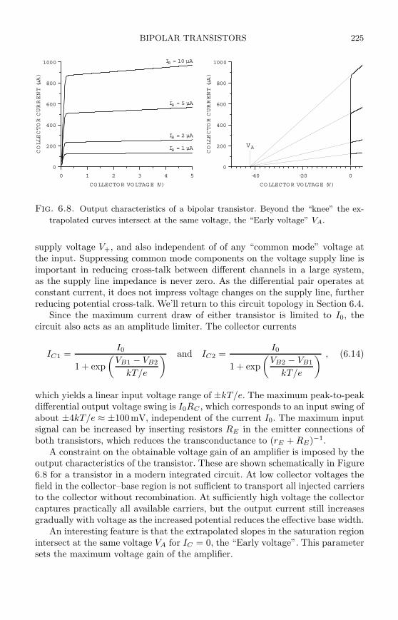
BIPOLAR TRANSISTORS 225
0 1 2 3 4 5
COLLECTOR VOLTAGE (V)
0
200
400
600
800
1000
COLLECTORCURRENT(µA)
-40 -20 0
COLLECTOR VOLTAGE (V)
0
200
400
600
800
1000
COLLECTORCURRENT(µA)
VAIB = 1 µA
IB = 2 µA
IB = 5 µA
IB = 10 µA
Fig. 6.8. Output characteristics of a bipolar transistor. Beyond the “knee” the ex-
trapolated curves intersect at the same voltage, the “Early voltage” VA.
supply voltage V+, and also independent of of any “common mode” voltage atthe input. Suppressing common mode components on the voltage supply line isimportant in reducing cross-talk between different channels in a large system,as the supply line impedance is never zero. As the differential pair operates atconstant current, it does not impress voltage changes on the supply line, furtherreducing potential cross-talk. We’ll return to this circuit topology in Section 6.4.
Since the maximum current draw of either transistor is limited to I0, thecircuit also acts as an amplitude limiter. The collector currents
IC1 =I0
1 + exp
(
VB1 − VB2
kT/e
) and IC2 =I0
1 + exp
(
VB2 − VB1
kT/e
) , (6.14)
which yields a linear input voltage range of ±kT/e. The maximum peak-to-peakdifferential output voltage swing is I0RC , which corresponds to an input swing ofabout ±4kT/e ≈ ±100mV, independent of the current I0. The maximum inputsignal can be increased by inserting resistors RE in the emitter connections ofboth transistors, which reduces the transconductance to (rE + RE)−1.
A constraint on the obtainable voltage gain of an amplifier is imposed by theoutput characteristics of the transistor. These are shown schematically in Figure6.8 for a transistor in a modern integrated circuit. At low collector voltages thefield in the collector–base region is not sufficient to transport all injected carriersto the collector without recombination. At sufficiently high voltage the collectorcaptures practically all available carriers, but the output current still increasesgradually with voltage as the increased potential reduces the effective base width.
An interesting feature is that the extrapolated slopes in the saturation regionintersect at the same voltage VA for IC = 0, the “Early voltage”. This parametersets the maximum voltage gain of the amplifier.
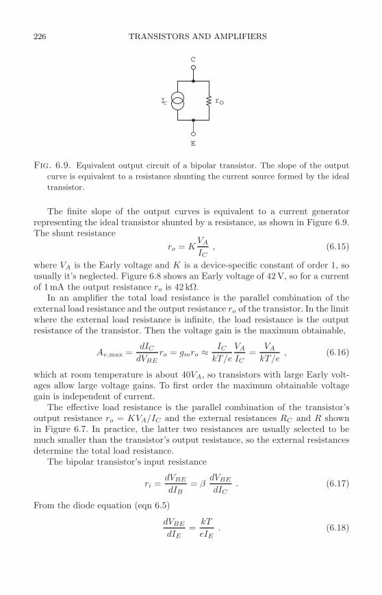
226 TRANSISTORS AND AMPLIFIERS
IC ro
C
E
Fig. 6.9. Equivalent output circuit of a bipolar transistor. The slope of the output
curve is equivalent to a resistance shunting the current source formed by the ideal
transistor.
The finite slope of the output curves is equivalent to a current generatorrepresenting the ideal transistor shunted by a resistance, as shown in Figure 6.9.The shunt resistance
ro = KVA
IC, (6.15)
where VA is the Early voltage and K is a device-specific constant of order 1, sousually it’s neglected. Figure 6.8 shows an Early voltage of 42 V, so for a currentof 1mA the output resistance ro is 42 kΩ.
In an amplifier the total load resistance is the parallel combination of theexternal load resistance and the output resistance ro of the transistor. In the limitwhere the external load resistance is infinite, the load resistance is the outputresistance of the transistor. Then the voltage gain is the maximum obtainable,
Av,max =dIC
dVBEro = gmro ≈ IC
kT/e
VA
IC=
VA
kT/e, (6.16)
which at room temperature is about 40VA, so transistors with large Early volt-ages allow large voltage gains. To first order the maximum obtainable voltagegain is independent of current.
The effective load resistance is the parallel combination of the transistor’soutput resistance ro = KVA/IC and the external resistances RC and R shownin Figure 6.7. In practice, the latter two resistances are usually selected to bemuch smaller than the transistor’s output resistance, so the external resistancesdetermine the total load resistance.
The bipolar transistor’s input resistance
ri =dVBE
dIB= β
dVBE
dIC. (6.17)
From the diode equation (eqn 6.5)
dVBE
dIE=
kT
eIE. (6.18)
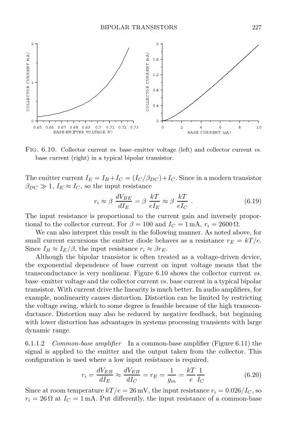
BIPOLAR TRANSISTORS 227
0.65 0.66 0.67 0.68 0.69 0.7 0.71 0.72 0.73BASE-EM ITTER VOLTAGE (V)
0
1
2
COLLECTORCURRENT(mA)
0 2 4 6 8 10BASE CURRENT (µA)
0
0.4
0.8
1.2
1.6
2
COLLECTORCURRENT(mA)
Fig. 6.10. Collector current vs. base–emitter voltage (left) and collector current vs.
base current (right) in a typical bipolar transistor.
The emitter current IE = IB +IC = (IC/βDC)+IC . Since in a modern transistorβDC ≫ 1, IE ≈ IC , so the input resistance
ri ≈ βdVBE
dIE= β
kT
eIE≈ β
kT
eIC. (6.19)
The input resistance is proportional to the current gain and inversely propor-tional to the collector current. For β = 100 and IC = 1mA, ri = 2600 Ω.
We can also interpret this result in the following manner. As noted above, forsmall current excursions the emitter diode behaves as a resistance rE = kT/e.Since IB ≈ IE/β, the input resistance ri ≈ βrE .
Although the bipolar transistor is often treated as a voltage-driven device,the exponential dependence of base current on input voltage means that thetransconductance is very nonlinear. Figure 6.10 shows the collector current vs.base–emitter voltage and the collector current vs. base current in a typical bipolartransistor. With current drive the linearity is much better. In audio amplifiers, forexample, nonlinearity causes distortion. Distortion can be limited by restrictingthe voltage swing, which to some degree is feasible because of the high transcon-ductance. Distortion may also be reduced by negative feedback, but beginningwith lower distortion has advantages in systems processing transients with largedynamic range.
6.1.1.2 Common-base amplifier In a common-base amplifier (Figure 6.11) thesignal is applied to the emitter and the output taken from the collector. Thisconfiguration is used where a low input resistance is required.
ri =dVEB
dIE≈ dVEB
dIC= rE =
1
gm=
kT
e
1
IC(6.20)
Since at room temperature kT/e = 26mV, the input resistance ri = 0.026/IC, sori = 26 Ω at IC = 1 mA. Put differently, the input resistance of a common-base
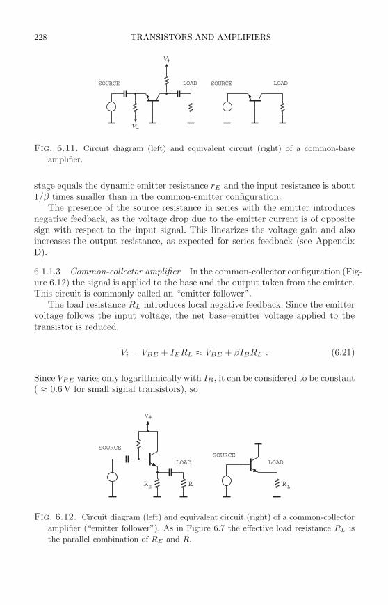
228 TRANSISTORS AND AMPLIFIERS
V
V
+
SOURCE SOURCELOAD LOAD
Fig. 6.11. Circuit diagram (left) and equivalent circuit (right) of a common-base
amplifier.
stage equals the dynamic emitter resistance rE and the input resistance is about1/β times smaller than in the common-emitter configuration.
The presence of the source resistance in series with the emitter introducesnegative feedback, as the voltage drop due to the emitter current is of oppositesign with respect to the input signal. This linearizes the voltage gain and alsoincreases the output resistance, as expected for series feedback (see AppendixD).
6.1.1.3 Common-collector amplifier In the common-collector configuration (Fig-ure 6.12) the signal is applied to the base and the output taken from the emitter.This circuit is commonly called an “emitter follower”.
The load resistance RL introduces local negative feedback. Since the emittervoltage follows the input voltage, the net base–emitter voltage applied to thetransistor is reduced,
Vi = VBE + IERL ≈ VBE + βIBRL . (6.21)
Since VBE varies only logarithmically with IB , it can be considered to be constant( ≈ 0.6 V for small signal transistors), so
V+
SOURCESOURCE
LOAD LOAD
RR R LE
Fig. 6.12. Circuit diagram (left) and equivalent circuit (right) of a common-collector
amplifier (“emitter follower”). As in Figure 6.7 the effective load resistance RL is
the parallel combination of RE and R.
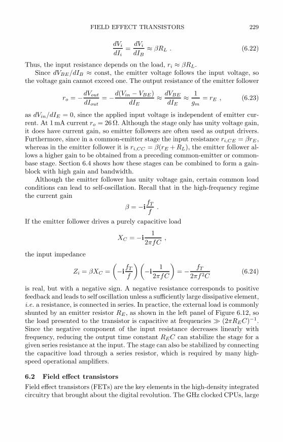
FIELD EFFECT TRANSISTORS 229
dVi
dIi=
dVi
dIB≈ βRL . (6.22)
Thus, the input resistance depends on the load, ri ≈ βRL.Since dVBE/dIB ≈ const, the emitter voltage follows the input voltage, so
the voltage gain cannot exceed one. The output resistance of the emitter follower
ro = −dVout
dIout= −d(Vin − VBE)
dIE≈ dVBE
dIE≈ 1
gm= rE , (6.23)
as dVin/dIE = 0, since the applied input voltage is independent of emitter cur-rent. At 1 mA current ro = 26 Ω. Although the stage only has unity voltage gain,it does have current gain, so emitter followers are often used as output drivers.Furthermore, since in a common-emitter stage the input resistance ri,CE = βrE ,whereas in the emitter follower it is ri,CC = β(rE + RL), the emitter follower al-lows a higher gain to be obtained from a preceding common-emitter or common-base stage. Section 6.4 shows how these stages can be combined to form a gain-block with high gain and bandwidth.
Although the emitter follower has unity voltage gain, certain common loadconditions can lead to self-oscillation. Recall that in the high-frequency regimethe current gain
β = −ifT
f.
If the emitter follower drives a purely capacitive load
XC = −i1
2πfC,
the input impedance
Zi = βXC =
(
−ifT
f
)(
−i1
2πfC
)
= − fT
2πf2C(6.24)
is real, but with a negative sign. A negative resistance corresponds to positivefeedback and leads to self oscillation unless a sufficiently large dissipative element,i.e. a resistance, is connected in series. In practice, the external load is commonlyshunted by an emitter resistor RE , as shown in the left panel of Figure 6.12, sothe load presented to the transistor is capacitive at frequencies ≫ (2πREC)−1.Since the negative component of the input resistance decreases linearly withfrequency, reducing the output time constant REC can stabilize the stage for agiven series resistance at the input. The stage can also be stabilized by connectingthe capacitive load through a series resistor, which is required by many high-speed operational amplifiers.
6.2 Field effect transistors
Field effect transistors (FETs) are the key elements in the high-density integratedcircuitry that brought about the digital revolution. The GHz clocked CPUs, large
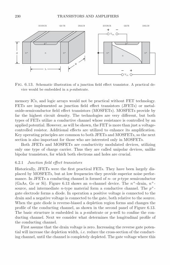
230 TRANSISTORS AND AMPLIFIERS
SOURCESOURCE DRAINDRAIN GATEGATE
n
p p
n nn+
+ +
++
V
V
DS
GS
L
W
nn
+d
Fig. 6.13. Schematic illustration of a junction field effect transistor. A practical de-
vice would be embedded in a p-substrate.
memory ICs, and logic arrays would not be practical without FET technology.FETs are implemented as junction field effect transistors (JFETs) or metal-oxide-semiconductor field effect transistors (MOSFETs). MOSFETs provide byfar the highest circuit density. The technologies are very different, but bothtypes of FETs utilize a conductive channel whose resistance is controlled by anapplied potential. However, as will be shown, the FET is more than just a voltage-controlled resistor. Additional effects are utilized to enhance its amplification.Key operating principles are common to both JFETs and MOSFETs, so the nextsection is also important for those who are interested only in MOSFETs.
Both JFETs and MOSFETs are conductivity modulated devices, utilizingonly one type of charge carrier. Thus they are called unipolar devices, unlikebipolar transistors, for which both electrons and holes are crucial.
6.2.1 Junction field effect transistors
Historically, JFETs were the first practical FETs. They have been largely dis-placed by MOSFETs, but at low frequencies they provide superior noise perfor-mance. In JFETs a conducting channel is formed of n- or p-type semiconductor(GaAs, Ge or Si). Figure 6.13 shows an n-channel device. The n+-drain, n+-source, and intermediate n-type material form a conductive channel. The p+-gate electrode forms a diode. In operation a positive voltage is connected to thedrain and a negative voltage is connected to the gate, both relative to the source.When the gate diode is reverse-biased a depletion region forms and changes theprofile of the conducting channel, as shown in the second panel of Figure 6.13.The basic structure is embedded in a p-substrate or p-well to confine the con-ducting channel. Next we consider what determines the longitudinal profile ofthe conducting channel.
First assume that the drain voltage is zero. Increasing the reverse gate poten-tial will increase the depletion width, i.e. reduce the cross-section of the conduct-ing channel, until the channel is completely depleted. The gate voltage where this
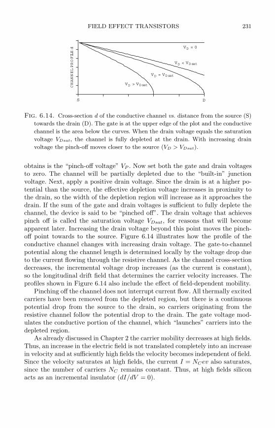
FIELD EFFECT TRANSISTORS 231
CHANNELPROFILEd
S D
VD = 0
VD < VD sat
VD = VD sat
VD > VD sat
Fig. 6.14. Cross-section d of the conductive channel vs. distance from the source (S)
towards the drain (D). The gate is at the upper edge of the plot and the conductive
channel is the area below the curves. When the drain voltage equals the saturation
voltage VDsat, the channel is fully depleted at the drain. With increasing drain
voltage the pinch-off moves closer to the source (VD > VDsat).
obtains is the “pinch-off voltage” VP . Now set both the gate and drain voltagesto zero. The channel will be partially depleted due to the “built-in” junctionvoltage. Next, apply a positive drain voltage. Since the drain is at a higher po-tential than the source, the effective depletion voltage increases in proximity tothe drain, so the width of the depletion region will increase as it approaches thedrain. If the sum of the gate and drain voltages is sufficient to fully deplete thechannel, the device is said to be “pinched off”. The drain voltage that achievespinch off is called the saturation voltage VDsat, for reasons that will becomeapparent later. Increasing the drain voltage beyond this point moves the pinch-off point towards to the source. Figure 6.14 illustrates how the profile of theconductive channel changes with increasing drain voltage. The gate-to-channelpotential along the channel length is determined locally by the voltage drop dueto the current flowing through the resistive channel. As the channel cross-sectiondecreases, the incremental voltage drop increases (as the current is constant),so the longitudinal drift field that determines the carrier velocity increases. Theprofiles shown in Figure 6.14 also include the effect of field-dependent mobility.
Pinching off the channel does not interrupt current flow. All thermally excitedcarriers have been removed from the depleted region, but there is a continuouspotential drop from the source to the drain, so carriers originating from theresistive channel follow the potential drop to the drain. The gate voltage mod-ulates the conductive portion of the channel, which “launches” carriers into thedepleted region.
As already discussed in Chapter 2 the carrier mobility decreases at high fields.Thus, an increase in the electric field is not translated completely into an increasein velocity and at sufficiently high fields the velocity becomes independent of field.Since the velocity saturates at high fields, the current I = NCev also saturates,since the number of carriers NC remains constant. Thus, at high fields siliconacts as an incremental insulator (dI/dV = 0).
232 TRANSISTORS AND AMPLIFIERS
0 0.5 1VD/VP
0
0.2
0.4
0.6
0.8
1
I D/I P
VG = 0
VG = VP/8
VG = VP/4
VG = VP/2
VD sat
Fig. 6.15. Operating regimes of a field effect transistor.
As the drain voltage is increased beyond pinch-off, the additional voltagedecreases the length of the resistive channel, but also increases the potential dropin the drain depletion region. As a result, the current increases only graduallywith drain voltage. This is a result of the changing potential distribution alongthe channel in combination with the “incremental insulator” properties of theregion between the conductive channel and the drain.
Although textbook equations for FET characteristics tend to use constantmobility, in reality velocity saturation is a key phenomenon in the mode whereFETs are typically operated. At fields above about 105 V/cm practically all ofthe energy imparted by an increased field goes into phonon emission, but themobility already decreases substantially at a field of 104 V/cm, corresponding to1V across 1 µm. Thus, the behavior of micron-scale devices is strongly affectedby nonconstant mobility, leading to smaller transconductance than predicted bya constant mobility model. Sze (1981) discusses this in more detail. Nevertheless,the following discussion uses the constant mobility model, as it illustrates thekey aspects.
6.2.1.1 Current–voltage characteristics In amplifiers the interesting operatingregime is beyond pinch-off, i.e. drain voltages > VDsat. JFET output character-istics are illustrated in Figure 6.15, showing the linear region, where the channelbehaves resistive, and the saturation region, where the device acts as a currentsource, i.e. exhibits a high output resistance. At very high drain voltages thedevice exhibits breakdown, whose onset is indicated by a rapid upturn in draincurrent.
1. “Linear Region”
At low drain and gate voltages, the resistive channel extends from the source tothe drain. The current–voltage characteristic
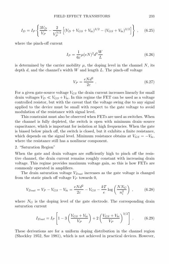
FIELD EFFECT TRANSISTORS 233
ID = IP
3VD
VP− 2
V3/2P
[
(VD + VGS + Vbi)3/2 − (VGS + Vbi)
3/2]
, (6.25)
where the pinch-off current
IP =1
6εµ(eN)2d3 W
L(6.26)
is determined by the carrier mobility µ, the doping level in the channel N , itsdepth d, and the channel’s width W and length L. The pinch-off voltage
VP =eNd2
2ε. (6.27)
For a given gate-source voltage VGS the drain current increases linearly for smalldrain voltages VD ≪ VGS +Vbi. In this regime the FET can be used as a voltagecontrolled resistor, but with the caveat that the voltage swing due to any signalapplied to the device must be small with respect to the gate voltage to avoidmodulation of the resistance with signal level.
This constraint must also be observed when FETs are used as switches. Whenthe channel is fully depleted, the switch is open with minimum drain–sourcecapacitance, which is important for isolation at high frequencies. When the gateis biased below pinch off, the switch is closed, but it exhibits a finite resistance,which depends on the signal level. Minimum resistance obtains at VGS = −Vbi,where the resistance still has a nonlinear component.
2. “Saturation Region”
When the gate and drain voltages are sufficiently high to pinch off the resis-tive channel, the drain current remains roughly constant with increasing drainvoltage. This regime provides maximum voltage gain, so this is how FETs arecommonly operated in amplifiers.
The drain saturation voltage VDsat increases as the gate voltage is changedfrom the static pinch off voltage VP towards 0,
VDsat = VP − VGS − Vbi =eNd2
2ε− VGS − kT
elog
(
NNG
n2i
)
, (6.28)
where NG is the doping level of the gate electrode. The corresponding drainsaturation current
IDsat = IP
[
1 − 3
(
VGS + Vbi
VP
)
+ 2
(
VGS + Vbi
VP
)3/2]
. (6.29)
These derivations are for a uniform doping distribution in the channel region(Shockley 1952, Sze 1981), which is not achieved in practical devices. However,
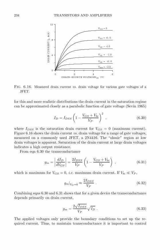
234 TRANSISTORS AND AMPLIFIERS
0 2 4 6DRAIN-SOURCE VOLTAGE VDS (V)
0
4
8
12
DRAIN
CURRENTI D
(mA)
VGS = 0
VGS = -0.5
VGS = -1.0
VGS = -1.5
VGS = -2.0
VGS = -2.5
Fig. 6.16. Measured drain current vs. drain voltage for various gate voltages of a
JFET.
for this and more realistic distributions the drain current in the saturation regimecan be approximated closely as a parabolic function of gate voltage (Sevin 1965)
ID = IDSS
(
1 − VGS + Vbi
VP
)2
, (6.30)
where IDSS is the saturation drain current for VGS = 0 (maximum current).Figure 6.16 shows the drain current vs. drain voltage for a range of gate voltages,measured on a commonly used JFET, a 2N4416. The “ohmic” region at lowdrain voltages is apparent. Saturation of the drain current at large drain voltagesindicates a high output resistance.
From eqn 6.30 the transconductance
gm =
∣
∣
∣
∣
dID
dVGS
∣
∣
∣
∣
=2IDSS
VP
(
1 − VGS + Vbi
VP
)
, (6.31)
which is maximum for VGS = 0, i.e. maximum drain current. If Vbi ≪ VP ,
gm|VG=0 ≈ 2IDSS
VP. (6.32)
Combining eqns 6.30 and 6.31 shows that for a given device the transconductancedepends primarily on drain current,
gm =2√
IDSS
VP
√
ID . (6.33)
The applied voltages only provide the boundary conditions to set up the re-quired current. Thus, to maintain transconductance it is important to control
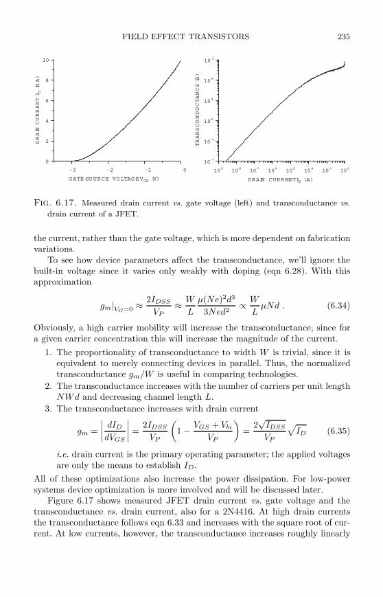
FIELD EFFECT TRANSISTORS 235
-3 -2 -1 0
G ATE-SO URCE VO LTAG E VGS (V)
0
2
4
6
8
10
DRAIN
CURRENTI D
(mA)
10-9
10-8
10-7
10-6
10-5
10-4
10-3
10-2
DRAIN CURRENT ID (A)
10-7
10-6
10-5
10-4
10-3
10-2
TRANSCONDUCTANCE(S)
Fig. 6.17. Measured drain current vs. gate voltage (left) and transconductance vs.
drain current of a JFET.
the current, rather than the gate voltage, which is more dependent on fabricationvariations.
To see how device parameters affect the transconductance, we’ll ignore thebuilt-in voltage since it varies only weakly with doping (eqn 6.28). With thisapproximation
gm|VG=0 ≈ 2IDSS
VP≈ W
L
µ(Ne)2d3
3Ned2∝ W
LµNd . (6.34)
Obviously, a high carrier mobility will increase the transconductance, since fora given carrier concentration this will increase the magnitude of the current.
1. The proportionality of transconductance to width W is trivial, since it isequivalent to merely connecting devices in parallel. Thus, the normalizedtransconductance gm/W is useful in comparing technologies.
2. The transconductance increases with the number of carriers per unit lengthNWd and decreasing channel length L.
3. The transconductance increases with drain current
gm =
∣
∣
∣
∣
dID
dVGS
∣
∣
∣
∣
=2IDSS
VP
(
1 − VGS + Vbi
VP
)
=2√
IDSS
VP
√
ID (6.35)
i.e. drain current is the primary operating parameter; the applied voltagesare only the means to establish ID.
All of these optimizations also increase the power dissipation. For low-powersystems device optimization is more involved and will be discussed later.
Figure 6.17 shows measured JFET drain current vs. gate voltage and thetransconductance vs. drain current, also for a 2N4416. At high drain currentsthe transconductance follows eqn 6.33 and increases with the square root of cur-rent. At low currents, however, the transconductance increases roughly linearly
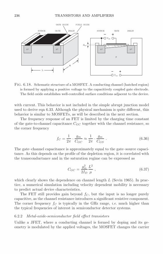
236 TRANSISTORS AND AMPLIFIERS
SOURCE SOURCEDRAIN DRAINGATE GATE
n
p p
n+ +
V
V
DS
GS
L
W
n+ n+
GATE OXIDE
dox
FIELD OXIDE
Fig. 6.18. Schematic structure of a MOSFET. A conducting channel (hatched region)
is formed by applying a positive voltage to the capacitively coupled gate electrode.
The field oxide establishes well-controlled surface conditions adjacent to the device.
with current. This behavior is not included in the simple abrupt junction modelused to derive eqn 6.33. Although the physical mechanism is quite different, thisbehavior is similar to MOSFETs, as will be described in the next section.
The frequency response of an FET is limited by the charging time constantof the gate-to-channel capacitance CGC together with the channel resistance, sothe corner frequency
fC =1
2π· gm
CGC≈ 1
2π· gm
CGS. (6.36)
The gate–channel capacitance is approximately equal to the gate–source capaci-tance. As this depends on the profile of the depletion region, it is correlated withthe transconductance and in the saturation regime can be expressed as
CGC =g2
m
2ID
L2
µ, (6.37)
which clearly shows the dependence on channel length L (Sevin 1965). In prac-tice, a numerical simulation including velocity dependent mobility is necessaryto predict actual device characteristics.
The FET still provides gain beyond fC , but the input is no longer purelycapacitive, as the channel resistance introduces a significant resistive component.The corner frequency fC is typically in the GHz range, i.e. much higher thanthe typical frequencies of interest in semiconductor detector systems.
6.2.2 Metal-oxide-semiconductor field effect transistors
Unlike a JFET, where a conducting channel is formed by doping and its ge-ometry is modulated by the applied voltages, the MOSFET changes the carrier
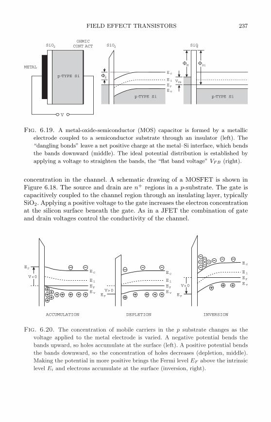
FIELD EFFECT TRANSISTORS 237
E
EE
V
E
c
i
F
FB
v
p-TYPE Si
p-TYPE Si p-TYPE Si
V
METAL
SiO SiO SiO2 2 2
OHMICCONT ACT
M Si
S
Fig. 6.19. A metal-oxide-semiconductor (MOS) capacitor is formed by a metallic
electrode coupled to a semiconductor substrate through an insulator (left). The
“dangling bonds” leave a net positive charge at the metal–Si interface, which bends
the bands downward (middle). The ideal potential distribution is established by
applying a voltage to straighten the bands, the “flat band voltage” VFB (right).
concentration in the channel. A schematic drawing of a MOSFET is shown inFigure 6.18. The source and drain are n+ regions in a p-substrate. The gate iscapacitively coupled to the channel region through an insulating layer, typicallySiO2. Applying a positive voltage to the gate increases the electron concentrationat the silicon surface beneath the gate. As in a JFET the combination of gateand drain voltages control the conductivity of the channel.
E
E
E
E
E
EE
E
E
E E
E
E
E
E
c
c
c
i
i
i
F
F
F
F F
F
v
v
vV>0
V>0
V<0
ACCUMULATION DEPLETION INVERSION
Fig. 6.20. The concentration of mobile carriers in the p substrate changes as the
voltage applied to the metal electrode is varied. A negative potential bends the
bands upward, so holes accumulate at the surface (left). A positive potential bends
the bands downward, so the concentration of holes decreases (depletion, middle).
Making the potential in more positive brings the Fermi level EF above the intrinsic
level Ei and electrons accumulate at the surface (inversion, right).
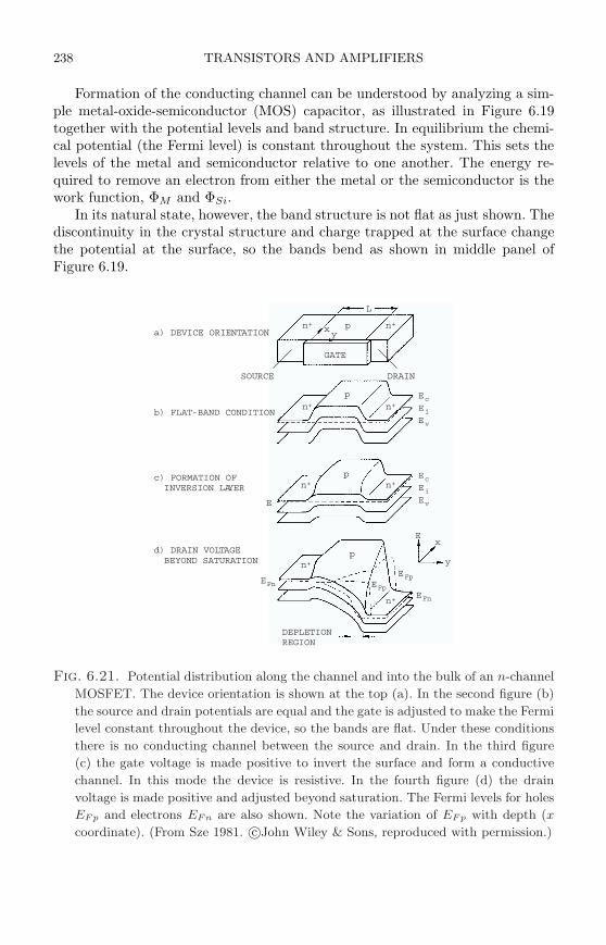
238 TRANSISTORS AND AMPLIFIERS
Formation of the conducting channel can be understood by analyzing a sim-ple metal-oxide-semiconductor (MOS) capacitor, as illustrated in Figure 6.19together with the potential levels and band structure. In equilibrium the chemi-cal potential (the Fermi level) is constant throughout the system. This sets thelevels of the metal and semiconductor relative to one another. The energy re-quired to remove an electron from either the metal or the semiconductor is thework function, ΦM and ΦSi.
In its natural state, however, the band structure is not flat as just shown. Thediscontinuity in the crystal structure and charge trapped at the surface changethe potential at the surface, so the bands bend as shown in middle panel ofFigure 6.19.
L
GATE
SOURCE DRAIN
n
n
n
n
n
n
n
n
p
p
p
p
+
+
+
+
+
+
+
+
a) DEVICE ORIENTATION
b) FLAT-BAND CONDITION
c) FORMATION OFINVERSION LAYER
d) DRAIN VOLTAGEBEYOND SATURATION
E
E
E
E
E
E
EE
E
E
c
c
i
i
v
v
Fp
Fp
Fn
Fn
E
x
y
E
DEPLETIONREGION
xy
Fig. 6.21. Potential distribution along the channel and into the bulk of an n-channel
MOSFET. The device orientation is shown at the top (a). In the second figure (b)
the source and drain potentials are equal and the gate is adjusted to make the Fermi
level constant throughout the device, so the bands are flat. Under these conditions
there is no conducting channel between the source and drain. In the third figure
(c) the gate voltage is made positive to invert the surface and form a conductive
channel. In this mode the device is resistive. In the fourth figure (d) the drain
voltage is made positive and adjusted beyond saturation. The Fermi levels for holes
EFp and electrons EFn are also shown. Note the variation of EFp with depth (x
coordinate). (From Sze 1981. c©John Wiley & Sons, reproduced with permission.)
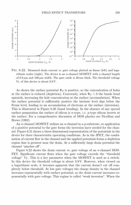
FIELD EFFECT TRANSISTORS 239
0 0.5 1 1.5 2
GATE VOLTAGE VGS (V)
0
1
2
3
4
5
6
DRAIN
CURRENT(mA)
0 0.4 0.8 1.2 1.6 2GATE VOLTAGE VGS (V)
10-10
10-9
10-8
10-7
10-6
10-5
10-4
10-3
10-2
DRAIN
CURRENT(A)
Fig. 6.22. Measured drain current vs. gate voltage plotted on linear (left) and loga-
rithmic scales (right). The device is an n-channel MOSFET with a channel length
of 0.8 µm and 100 µm width. The gate oxide is 20 nm thick. The threshold voltage
VT of this device is about 0.9 V.
As shown the surface potential ΦS is positive, so the concentration of holesat the surface is reduced (depletion). Conversely, when ΦS < 0 the bands bendupwards, increasing the hole concentration at the surface (accumulation). Whenthe surface potential is sufficiently positive the intrinsic level dips below theFermi level, leading to an accumulation of electrons at the surface (inversion).This is illustrated in Figure 6.20 (band bending). In the absence of any specialsurface preparation the surface of silicon is n-type, i.e. p-type silicon inverts atthe surface. For a comprehensive discussion of MOS physics see Nicollian andBrews (1982).
An n-channel MOSFET utilizes an n-channel in a p-substrate, so applicationof a positive potential to the gate forms the inversion layer needed for the chan-nel. Figure 6.21 shows a three-dimensional representation of the potentials in thedevice for three characteristic operating conditions. As in the JFET, the combi-nation of current flow in the channel and the applied potentials forms a depletionregion that is greatest near the drain. At a sufficiently large drain potential thechannel “pinches off”.
Figure 6.22 shows the drain current vs. gate voltage of an n-channel MOS-FET. Significant current flows when the gate voltage exceeds the “thresholdvoltage” VT . This is a key parameter when the MOSFET is used as a switch.In this device the threshold voltage is about 0.9V. However, when viewed ona logarithmic scale, it becomes apparent that the current doesn’t cut off com-pletely below threshold. At low gate voltages the charge density in the channelincreases exponentially with surface potential, so the drain current increases ex-ponentially with gate voltage. This regime is called “weak inversion”. When the
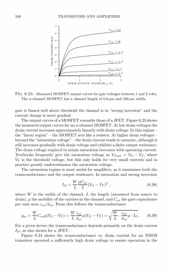
240 TRANSISTORS AND AMPLIFIERS
0 1 2 3DRAIN-SOURCE VOLTAGE VD S (V)
0
1
2
3
4
5
6
7
DRAIN
CURRENT(mA)
VG S = 1.0
VG S = 1.2
VG S = 1.4
VG S = 1.6
VG S = 1.8
VG S = 2.0
Fig. 6.23. Measured MOSFET output curves for gate voltages between 1 and 2 volts.
The n-channel MOSFET has a channel length of 0.8 µm and 100 µm width.
gate is biased well above threshold the channel is in “strong inversion” and thecurrent change is more gradual.
The output curves of a MOSFET resemble those of a JFET. Figure 6.23 showsthe measured output curves for an n-channel MOSFET. At low drain voltages thedrain current increases approximately linearly with drain voltage. In this regime –the “linear region” – the MOSFET acts like a resistor. At higher drain voltages –beyond the “saturation voltage” – the drain current tends to saturate, although itstill increases gradually with drain voltage and exhibits a finite output resistance.The drain voltage required to attain saturation increases with operating current.Textbooks frequently give the saturation voltage as VDsat = VG − VT , whereVT is the threshold voltage, but this only holds for very small currents and inpractice grossly underestimates the saturation voltage.
The saturation regime is most useful for amplifiers, as it maximizes both thetransconductance and the output resistance. In saturation and strong inversion
ID =W
L
µCox
2(VG − VT )2 , (6.38)
where W is the width of the channel, L the length (measured from source todrain), µ the mobility of the carriers in the channel, and Cox the gate capacitanceper unit area εox/dox. From this follows the transconductance
gm =W
LCoxµ(VG − VT ) =
W
L
εox
doxµ(VG − VT ) =
√
W
L· εox
doxµ · ID . (6.39)
For a given device the transconductance depends primarily on the drain currentID, as also shown for a JFET.
Figure 6.24 shows the transconductance vs. drain current for an NMOStransistor operated a sufficiently high drain voltage to ensure operation in the
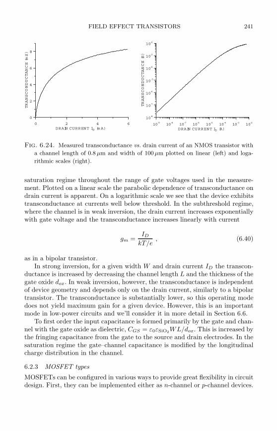
FIELD EFFECT TRANSISTORS 241
0 2 4 6DRAIN CURRENT ID (m A)
0
2
4
6
8
TRANSCONDUCTANCE(mS)
10-9
10-8
10-7
10-6
10-5
10-4
10-3
10-2
DRAIN CURRENT ID (A)
10-8
10-7
10-6
10-5
10-4
10-3
10-2
TRANSCONDUCTANCE(S)
Fig. 6.24. Measured transconductance vs. drain current of an NMOS transistor with
a channel length of 0.8 µm and width of 100 µm plotted on linear (left) and loga-
rithmic scales (right).
saturation regime throughout the range of gate voltages used in the measure-ment. Plotted on a linear scale the parabolic dependence of transconductance ondrain current is apparent. On a logarithmic scale we see that the device exhibitstransconductance at currents well below threshold. In the subthreshold regime,where the channel is in weak inversion, the drain current increases exponentiallywith gate voltage and the transconductance increases linearly with current
gm =ID
kT/e, (6.40)
as in a bipolar transistor.In strong inversion, for a given width W and drain current ID the transcon-
ductance is increased by decreasing the channel length L and the thickness of thegate oxide dox. In weak inversion, however, the transconductance is independentof device geometry and depends only on the drain current, similarly to a bipolartransistor. The transconductance is substantially lower, so this operating modedoes not yield maximum gain for a given device. However, this is an importantmode in low-power circuits and we’ll consider it in more detail in Section 6.6.
To first order the input capacitance is formed primarily by the gate and chan-nel with the gate oxide as dielectric, CGS = ε0εSiO2
WL/dox. This is increased bythe fringing capacitance from the gate to the source and drain electrodes. In thesaturation regime the gate–channel capacitance is modified by the longitudinalcharge distribution in the channel.
6.2.3 MOSFET types
MOSFETs can be configured in various ways to provide great flexibility in circuitdesign. First, they can be implemented either as n-channel or p-channel devices.
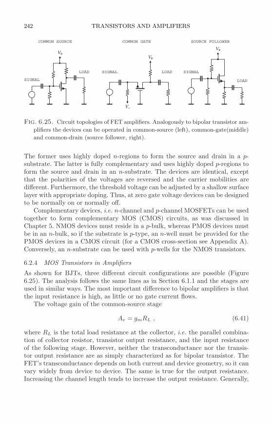
242 TRANSISTORS AND AMPLIFIERS
V+
SIGNAL
LOAD
V+
SIGNAL
LOAD
V
V
+
SIGNAL LOAD
COMMON SOURCE COMMON GATE SOURCE FOLLOWER
Fig. 6.25. Circuit topologies of FET amplifiers. Analogously to bipolar transistor am-
plifiers the devices can be operated in common-source (left), common-gate(middle)
and common-drain (source follower, right).
The former uses highly doped n-regions to form the source and drain in a p-substrate. The latter is fully complementary and uses highly doped p-regions toform the source and drain in an n-substrate. The devices are identical, exceptthat the polarities of the voltages are reversed and the carrier mobilities aredifferent. Furthermore, the threshold voltage can be adjusted by a shallow surfacelayer with appropriate doping. Thus, at zero gate voltage devices can be designedto be normally on or normally off.
Complementary devices, i.e. n-channel and p-channel MOSFETs can be usedtogether to form complementary MOS (CMOS) circuits, as was discussed inChapter 5. NMOS devices must reside in a p-bulk, whereas PMOS devices mustbe in an n-bulk, so if the substrate is p-type, an n-well must be provided for thePMOS devices in a CMOS circuit (for a CMOS cross-section see Appendix A).Conversely, an n-substrate can be used with p-wells for the NMOS transistors.
6.2.4 MOS Transistors in Amplifiers
As shown for BJTs, three different circuit configurations are possible (Figure6.25). The analysis follows the same lines as in Section 6.1.1 and the stages areused in similar ways. The most important difference to bipolar amplifiers is thatthe input resistance is high, as little or no gate current flows.
The voltage gain of the common-source stage
Av = gmRL , (6.41)
where RL is the total load resistance at the collector, i.e. the parallel combina-tion of collector resistor, transistor output resistance, and the input resistanceof the following stage. However, neither the transconductance nor the transis-tor output resistance are as simply characterized as for bipolar transistor. TheFET’s transconductance depends on both current and device geometry, so it canvary widely from device to device. The same is true for the output resistance.Increasing the channel length tends to increase the output resistance. Generally,
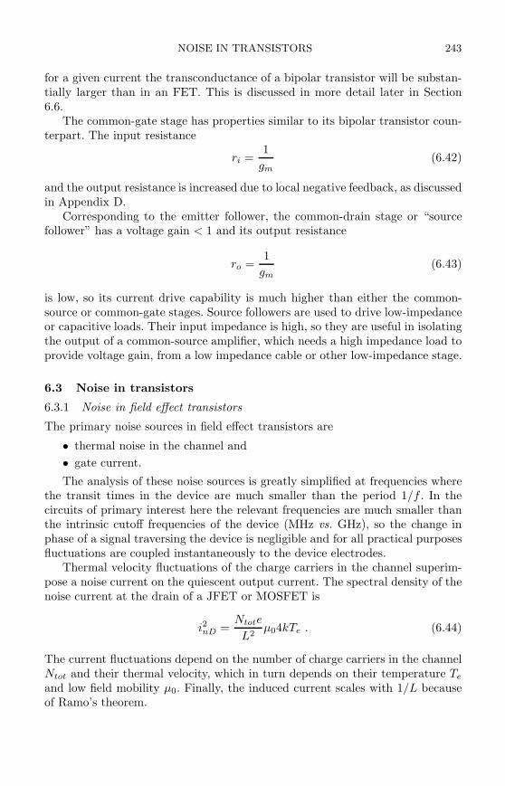
NOISE IN TRANSISTORS 243
for a given current the transconductance of a bipolar transistor will be substan-tially larger than in an FET. This is discussed in more detail later in Section6.6.
The common-gate stage has properties similar to its bipolar transistor coun-terpart. The input resistance
ri =1
gm(6.42)
and the output resistance is increased due to local negative feedback, as discussedin Appendix D.
Corresponding to the emitter follower, the common-drain stage or “sourcefollower” has a voltage gain < 1 and its output resistance
ro =1
gm(6.43)
is low, so its current drive capability is much higher than either the common-source or common-gate stages. Source followers are used to drive low-impedanceor capacitive loads. Their input impedance is high, so they are useful in isolatingthe output of a common-source amplifier, which needs a high impedance load toprovide voltage gain, from a low impedance cable or other low-impedance stage.
6.3 Noise in transistors
6.3.1 Noise in field effect transistors
The primary noise sources in field effect transistors are
• thermal noise in the channel and
• gate current.
The analysis of these noise sources is greatly simplified at frequencies wherethe transit times in the device are much smaller than the period 1/f . In thecircuits of primary interest here the relevant frequencies are much smaller thanthe intrinsic cutoff frequencies of the device (MHz vs. GHz), so the change inphase of a signal traversing the device is negligible and for all practical purposesfluctuations are coupled instantaneously to the device electrodes.
Thermal velocity fluctuations of the charge carriers in the channel superim-pose a noise current on the quiescent output current. The spectral density of thenoise current at the drain of a JFET or MOSFET is
i2nD =Ntote
L2µ04kTe . (6.44)
The current fluctuations depend on the number of charge carriers in the channelNtot and their thermal velocity, which in turn depends on their temperature Te
and low field mobility µ0. Finally, the induced current scales with 1/L becauseof Ramo’s theorem.
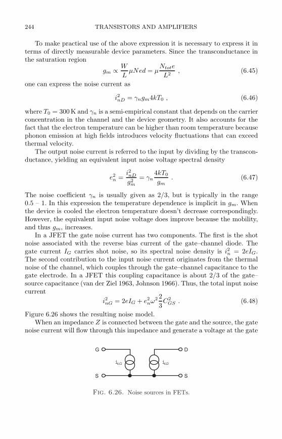
244 TRANSISTORS AND AMPLIFIERS
To make practical use of the above expression it is necessary to express it interms of directly measurable device parameters. Since the transconductance inthe saturation region
gm ∝ W
LµNed = µ
Ntote
L2, (6.45)
one can express the noise current as
i2nD = γngm4kT0 , (6.46)
where T0 = 300 K and γn is a semi-empirical constant that depends on the carrierconcentration in the channel and the device geometry. It also accounts for thefact that the electron temperature can be higher than room temperature becausephonon emission at high fields introduces velocity fluctuations that can exceedthermal velocity.
The output noise current is referred to the input by dividing by the transcon-ductance, yielding an equivalent input noise voltage spectral density
e2n =
i2nD
g2m
= γn4kT0
gm. (6.47)
The noise coefficient γn is usually given as 2/3, but is typically in the range0.5 – 1. In this expression the temperature dependence is implicit in gm. Whenthe device is cooled the electron temperature doesn’t decrease correspondingly.However, the equivalent input noise voltage does improve because the mobility,and thus gm, increases.
In a JFET the gate noise current has two components. The first is the shotnoise associated with the reverse bias current of the gate–channel diode. Thegate current IG carries shot noise, so its spectral noise density is i2n = 2eIG.The second contribution to the input noise current originates from the thermalnoise of the channel, which couples through the gate–channel capacitance to thegate electrode. In a JFET this coupling capacitance is about 2/3 of the gate–source capacitance (van der Ziel 1963, Johnson 1966). Thus, the total input noisecurrent
i2nG = 2eIG + e2nω2 2
3C2
GS . (6.48)
Figure 6.26 shows the resulting noise model.When an impedance Z is connected between the gate and the source, the gate
noise current will flow through this impedance and generate a voltage at the gate
G
S
D
S
i inG nD
Fig. 6.26. Noise sources in FETs.
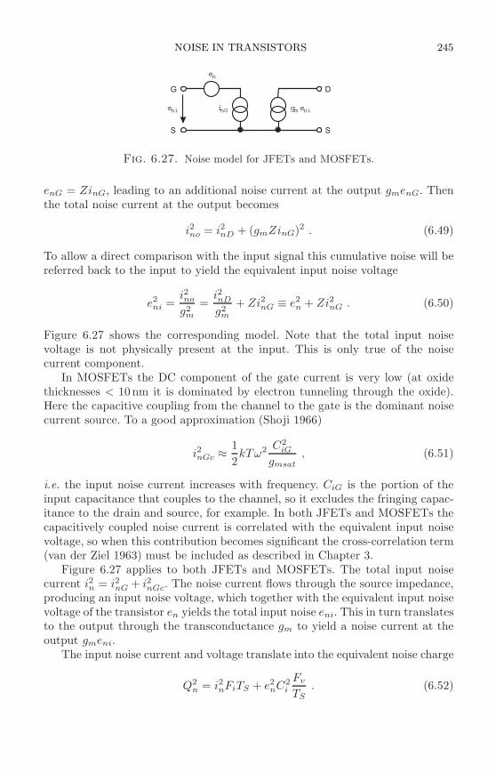
NOISE IN TRANSISTORS 245
G
S
D
S
i
e
g ee nG
n
m nini
Fig. 6.27. Noise model for JFETs and MOSFETs.
enG = ZinG, leading to an additional noise current at the output gmenG. Thenthe total noise current at the output becomes
i2no = i2nD + (gmZinG)2 . (6.49)
To allow a direct comparison with the input signal this cumulative noise will bereferred back to the input to yield the equivalent input noise voltage
e2ni =
i2no
g2m
=i2nD
g2m
+ Zi2nG ≡ e2n + Zi2nG . (6.50)
Figure 6.27 shows the corresponding model. Note that the total input noisevoltage is not physically present at the input. This is only true of the noisecurrent component.
In MOSFETs the DC component of the gate current is very low (at oxidethicknesses < 10nm it is dominated by electron tunneling through the oxide).Here the capacitive coupling from the channel to the gate is the dominant noisecurrent source. To a good approximation (Shoji 1966)
i2nGc ≈1
2kTω2 C2
iG
gmsat, (6.51)
i.e. the input noise current increases with frequency. CiG is the portion of theinput capacitance that couples to the channel, so it excludes the fringing capac-itance to the drain and source, for example. In both JFETs and MOSFETs thecapacitively coupled noise current is correlated with the equivalent input noisevoltage, so when this contribution becomes significant the cross-correlation term(van der Ziel 1963) must be included as described in Chapter 3.
Figure 6.27 applies to both JFETs and MOSFETs. The total input noisecurrent i2n = i2nG + i2nGc. The noise current flows through the source impedance,producing an input noise voltage, which together with the equivalent input noisevoltage of the transistor en yields the total input noise eni. This in turn translatesto the output through the transconductance gm to yield a noise current at theoutput gmeni.
The input noise current and voltage translate into the equivalent noise charge
Q2n = i2nFiTS + e2
nC2i
Fv
TS. (6.52)
246 TRANSISTORS AND AMPLIFIERS
For a representative JFET gm = 0.02 S, Ci = 10 pF, and IG < 150 pA. If we setFi = Fv = 1,
Q2n = 1.9 · 109
[
e2/s]
TS +3.25 · 10−3
[
e2 s]
TS. (6.53)
As the shaping time TS decreases, the current noise contribution decreases andthe voltage noise contribution increases. For TS = 1 µs the current contributionis 44 e and the voltage contribution 57 e, so the two contributions are roughlyequal.
6.3.1.1 Optimization of device geometry For a given device technology andnormalized operating current ID/W both the transconductance and the inputcapacitance are proportional to device width W , so that the ratio
gm
Ci= const . (6.54)
Then the signal-to-noise ratio can be written as
(
S
N
)2
=(Qs/C)2
e2n
=Q2
s
(Cd + Ci)2gm
4kT0∆f(
S
N
)2
=Q2
s
∆f
1
4kT0
(
gm
Ci
)
1
Ci
(
1 +Cd
Ci
)2 . (6.55)
From this we see that S/N is maximized when Ci = Cd (capacitive matching).When Ci ≪ Cd, the detector capacitance dominates, so the effect of in-
creased transistor capacitance is negligible. As the device width is increased thetransconductance increases and the equivalent noise voltage decreases, so S/Nimproves. When Ci > Cd the equivalent input noise voltage decreases as thedevice width is increased, but only with 1/
√W ∝ 1/
√Ci, so the increase in
capacitance overrides, decreasing S/N . Note that capacitive matching relies onthe linkage between device width and transconductance. Merely increasing thedevice capacitance without a corresponding decrease in noise brings no benefit.Adapting the device to the sensor can be accomplished by connecting transistorsin parallel or by selecting the device width, as described in Section 6.6.
6.3.1.2 Minimum obtainable noise charge Device scaling can be used to de-termine the minimum obtainable noise charge for a given device technology. Thetransconductance of an FET increases with drain current as shown in Figure6.24. However, noise only decreases up to a certain current. The reason is thatthe noise from parasitic source and gate resistances becomes significant. Further-more, since the equivalent noise charge depends on the total capacitance at theinput node, we must consider not just the gate–channel capacitance, but alsoany other parasitic capacitances associated with the device structure.
NOISE IN TRANSISTORS 247
Assume that a transistor of width W assumes its minimum noise at a currentID with an associated transconductance gm. Since the parasitic gate and sourceresistances are both inversely proportional to device width, the optimum currentdensity ID/W will be the same for all widths of transistors using the sametechnology (and device length). Thus, to obtain minimum noise one can tailorthe FET to a given detector by scaling the device width and keeping the currentdensity ID/W constant.
Within this framework one can characterize the device technology by thenormalized transconductance and input capacitance
g′m =gm
Wand C ′
i =Ci
W(6.56)
and use these quantities to scale to any other device width. Since the equivalentinput noise voltage
e2n ∝ 1
gm, (6.57)
the normalized input noise voltage is
e′n = en
√W . (6.58)
Using these quantities the equivalent noise charge can be written as
Q2n = 4kT0
γn
Wg′m
Fv
TS(Cd + Cs + WC ′
i)2 , (6.59)
where Cs is any stray capacitance present at the input in addition to the detectorcapacitance Cd and the FET capacitance WC ′
i . For WC ′i = Cd + Cs the noise
attains its minimum value
Qn,min =
√
16kT0
κn
Fv
TS(Cd + Cs) , (6.60)
whereκn ≡ gm
γnCi(6.61)
is a figure of merit for the noise performance of the FET. Note that the deviceinput capacitance WC ′
i includes the gate–channel capacitance and the fringingcapacitance from the gate to the source and drain.
As an example, an n-channel CMOS transistor with 1.2 µm channel lengthat a current density ID/W = 0.3 A/m has a ratio of transconductance to inputcapacitance ratio gm/Ci = 3 · 109 s−1. Assume γn = 1. Using a CR-RC shaperwith a 20ns shaping time and an external capacitance Cd + Cs = 7.5 pF, theminimum noise Qn,min = 88 aC = 546 e, achieved at a device width W = 5 mm,and a drain current of 1.5mA.
The obtainable noise improves with the inverse square root of the shapingtime, up to the point where 1/f noise becomes significant. For example, at TS =1 µs, the minimum noise Qn,min = 12 aC = 77 e, although in practice additionalnoise contributions will increase the obtainable noise beyond this value.
248 TRANSISTORS AND AMPLIFIERS
6.3.2 Low-frequency excess noise (“1/f noise”)
The preceding discussion has neglected 1/f noise, which adds a constant contri-bution independent of shaping time
Q2nf ∝ AfC2 . (6.62)
Although excess low-frequency noise is determined primarily by the concentra-tion of unwanted impurities and other defects, their effect in a specific technologyis also affected by device size. For some forms of 1/f noise
Af =Kf
WLC2G
, (6.63)
where CG is the gate–channel capacitance per unit area, and Kf is an empiri-cal constant that is device and process dependent. Typical values of the noiseconstant for various device types are
p-MOSFET Kf ≈ 2 · 10−32 C2/cm2
n-MOSFET Kf ≈ 5 · 10−31 C2/cm2
JFET Kf ≈ 10−33 C2/cm2
Specific implementations can improve on these values. One should note thatthis model is not universally applicable, since excess noise usually does not ex-hibit a pure 1/f dependence; especially in PMOS devices one often finds severalslopes. In practice, one must test the applicability of this parameterization bycomparing it with data before applying it to scaled amplifiers. Nevertheless, asa general rule, devices with larger gate area W · L tend to exhibit better “1/f”noise characteristics.
The frequency where the “1/f” noise intersects the white noise, the “cornerfrequency” fc = Af/e2
n, is often used as a measure of “1/f” noise. However, thiscan be misleading, as for the same level of “1/f” noise a higher white noise levelwill reduce the corner frequency. FETs typically exhibit noise corner frequenciesin the kHz range. Specially designed JFETs can do better, whereas in smallMOSFETs the noise corner can be in the range of hundreds of kHz.
6.3.3 Noise in bipolar transistors
In bipolar transistors the shot noise from the base current is important. As inFETs the transit times in modern bipolar transistors are much smaller thanshaping times of interest in our applications, so we can neglect frequency depen-dencies and the noise model is greatly simplified. The basic noise model shownin Figure 6.28 is the same as used for FETs, but the magnitude of the inputnoise current is much greater, as the base current will be 1 – 100µA rather than< 100 pA as in a JFET or fA in a MOSFET.
The base current noise is the shot noise associated with the component ofthe emitter current provided by the base.
i2nB = 2eIB . (6.64)
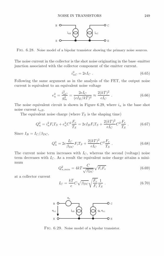
NOISE IN TRANSISTORS 249
B
E
C
E
i inB nC
Fig. 6.28. Noise model of a bipolar transistor showing the primary noise sources.
The noise current in the collector is the shot noise originating in the base–emitterjunction associated with the collector component of the emitter current.
i2nC = 2eIC . (6.65)
Following the same argument as in the analysis of the FET, the output noisecurrent is equivalent to an equivalent noise voltage
e2n =
i2nC
g2m
=2eIC
(eIE/kT )2≈ 2(kT )2
eIC. (6.66)
The noise equivalent circuit is shown in Figure 6.29, where in is the base shotnoise current inB .
The equivalent noise charge (where TS is the shaping time)
Q2n = i2nFiTS + e2
nC2 Fv
TS= 2eIBFiTS +
2(kT )2
eICC2 Fv
TS. (6.67)
Since IB = IC/βDC ,
Q2n = 2e
IC
βDCFiTS +
2(kT )2
eICC2 Fv
TS. (6.68)
The current noise term increases with IC , whereas the second (voltage) noiseterm decreases with IC . As a result the equivalent noise charge attains a mini-mum
Q2n,min = 4kT
C√βDC
√
FiFv (6.69)
at a collector current
IC =kT
eC√
βDC
√
Fv
Fi
1
TS. (6.70)
B
E
C
E
en
i g ee nB m nini
Fig. 6.29. Noise model of a bipolar transistor.
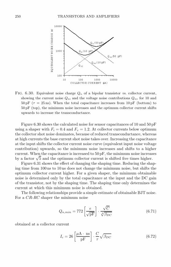
250 TRANSISTORS AND AMPLIFIERS
10 100 1000 10000COLLECTOR CURRENT (µA)
100
1000
10000
EQUIVALENTNOISECHARGE(e)
Q ni
Q nv(10 pF)
Q nv(50 pF)
Q n(10 pF)
Q n(50 pF)
Fig. 6.30. Equivalent noise charge Qn of a bipolar transistor vs. collector current,
showing the current noise Qni and the voltage noise contributions Qnv for 10 and
50 pF (τ = 25 ns). When the total capacitance increases from 10 pF (bottom) to
50 pF (top), the minimum noise increases and the optimum collector current shifts
upwards to increase the transconductance.
Figure 6.30 shows the calculated noise for sensor capacitances of 10 and 50pFusing a shaper with Fi = 0.4 and Fv = 1.2. At collector currents below optimumthe collector shot noise dominates, because of reduced transconductance, whereasat high currents the base current shot noise takes over. Increasing the capacitanceat the input shifts the collector current noise curve (equivalent input noise voltagecontribution) upwards, so the minimum noise increases and shifts to a highercurrent. When the capacitance is increased to 50pF, the minimum noise increasesby a factor
√5 and the optimum collector current is shifted five times higher.
Figure 6.31 shows the effect of changing the shaping time. Reducing the shap-ing time from 100ns to 10ns does not change the minimum noise, but shifts theoptimum collector current higher. For a given shaper, the minimum obtainablenoise is determined only by the total capacitance at the input and the DC gainof the transistor, not by the shaping time. The shaping time only determines thecurrent at which this minimum noise is obtained.
The following relationships provide a simple estimate of obtainable BJT noise.For a CR-RC shaper the minimum noise
Qn,min = 772
[
e√pF
]
·√
C4√
βDC(6.71)
obtained at a collector current
Ic = 26
[
µA · ns
pF
]
· C
τ
√
βDC (6.72)
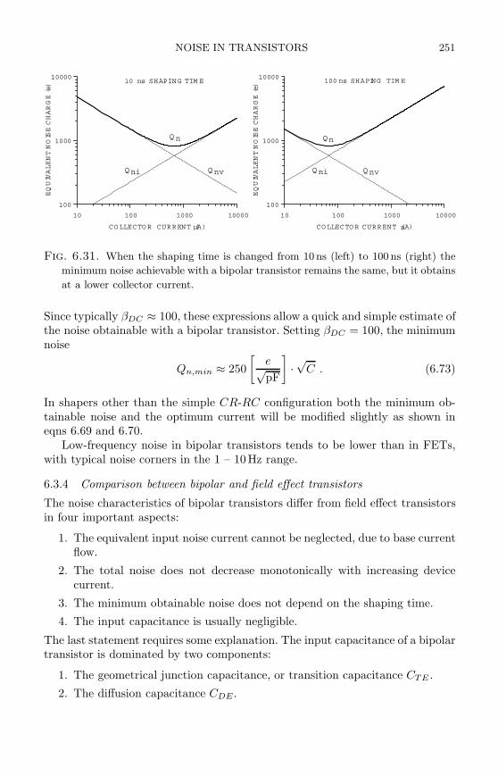
NOISE IN TRANSISTORS 251
10 100 1000 10000
CO LLECTOR CURRENT (µA)
100
1000
10000
EQUIVALENTNOISECHARGE(e)
Q ni Q nv
Q n
10 100 1000 10000
CO LLECTO R CURRENT (µA)
100
1000
10000
EQUIVALENTNOISECHARGE(e)
Q ni Q nv
Q n
100 ns SHAPING TIM E10 ns SHAPING TIM E
Fig. 6.31. When the shaping time is changed from 10 ns (left) to 100 ns (right) the
minimum noise achievable with a bipolar transistor remains the same, but it obtains
at a lower collector current.
Since typically βDC ≈ 100, these expressions allow a quick and simple estimate ofthe noise obtainable with a bipolar transistor. Setting βDC = 100, the minimumnoise
Qn,min ≈ 250
[
e√pF
]
·√
C . (6.73)
In shapers other than the simple CR-RC configuration both the minimum ob-tainable noise and the optimum current will be modified slightly as shown ineqns 6.69 and 6.70.
Low-frequency noise in bipolar transistors tends to be lower than in FETs,with typical noise corners in the 1 – 10Hz range.
6.3.4 Comparison between bipolar and field effect transistors
The noise characteristics of bipolar transistors differ from field effect transistorsin four important aspects:
1. The equivalent input noise current cannot be neglected, due to base currentflow.
2. The total noise does not decrease monotonically with increasing devicecurrent.
3. The minimum obtainable noise does not depend on the shaping time.
4. The input capacitance is usually negligible.
The last statement requires some explanation. The input capacitance of a bipolartransistor is dominated by two components:
1. The geometrical junction capacitance, or transition capacitance CTE .
2. The diffusion capacitance CDE .
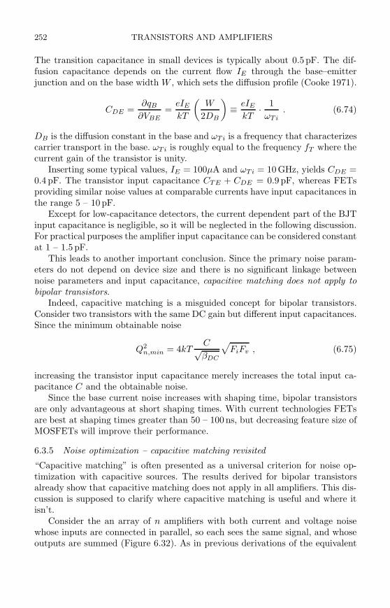
252 TRANSISTORS AND AMPLIFIERS
The transition capacitance in small devices is typically about 0.5 pF. The dif-fusion capacitance depends on the current flow IE through the base–emitterjunction and on the base width W , which sets the diffusion profile (Cooke 1971).
CDE =∂qB
∂VBE=
eIE
kT
(
W
2DB
)
≡ eIE
kT· 1
ωTi. (6.74)
DB is the diffusion constant in the base and ωTi is a frequency that characterizescarrier transport in the base. ωTi is roughly equal to the frequency fT where thecurrent gain of the transistor is unity.
Inserting some typical values, IE = 100µA and ωTi = 10 GHz, yields CDE =0.4 pF. The transistor input capacitance CTE + CDE = 0.9 pF, whereas FETsproviding similar noise values at comparable currents have input capacitances inthe range 5 – 10pF.
Except for low-capacitance detectors, the current dependent part of the BJTinput capacitance is negligible, so it will be neglected in the following discussion.For practical purposes the amplifier input capacitance can be considered constantat 1 – 1.5 pF.
This leads to another important conclusion. Since the primary noise param-eters do not depend on device size and there is no significant linkage betweennoise parameters and input capacitance, capacitive matching does not apply tobipolar transistors.
Indeed, capacitive matching is a misguided concept for bipolar transistors.Consider two transistors with the same DC gain but different input capacitances.Since the minimum obtainable noise
Q2n,min = 4kT
C√βDC
√
FiFv , (6.75)
increasing the transistor input capacitance merely increases the total input ca-pacitance C and the obtainable noise.
Since the base current noise increases with shaping time, bipolar transistorsare only advantageous at short shaping times. With current technologies FETsare best at shaping times greater than 50 – 100ns, but decreasing feature size ofMOSFETs will improve their performance.
6.3.5 Noise optimization – capacitive matching revisited
“Capacitive matching” is often presented as a universal criterion for noise op-timization with capacitive sources. The results derived for bipolar transistorsalready show that capacitive matching does not apply in all amplifiers. This dis-cussion is supposed to clarify where capacitive matching is useful and where itisn’t.
Consider the an array of n amplifiers with both current and voltage noisewhose inputs are connected in parallel, so each sees the same signal, and whoseoutputs are summed (Figure 6.32). As in previous derivations of the equivalent
NOISE IN TRANSISTORS 253
C
Q
d
s
S ,N1 1
S ,N1 1
S ,N1 1
S ,N1 1
S,N
Fig. 6.32. An array of amplifiers whose inputs are connected in parallel and outputs
are summed.
noise charge, we assume voltage-sensitive amplifiers with purely capacitive in-puts. Furthermore, to simplify the analysis, the amplifiers do not utilize feedback.
Of course, in considering the current and voltage noise contributions of thisamplifier array, one can follow a formal argument based on the noise charge
Q2n = i2nFiTS + e2
nC2 Fv
TS. (6.76)
Since the current noise contribution does not depend on capacitance, matchingthe amplifier input capacitance to the detector capacitance does not affect thisterm. On the other hand, since the voltage contribution does depend on ca-pacitance, a correlation between en and C can yield an optimization condition.To provide more insight into this argument, we’ll consider the signal and noisecontributions separately.
6.3.5.1 Current noise For the noise currents originating in the individual am-plifiers, the common connection to the signal source is a summing node, so ifin1 is the equivalent noise current of a single amplifier, for n amplifiers the totalinput noise current flowing through the signal source impedance is
in =√
n · in1 . (6.77)
The flow of this current through the input impedance Zi formed by the parallelconnection of the detector capacitance and amplifier capacitances gives rise to anoise voltage
vn = inZi . (6.78)
This voltage is applied in parallel to all amplifier inputs, so at the output of anindividual amplifier (assuming a gain A) the noise level is
N1(n) = Avn = A√
nin1Zi . (6.79)
254 TRANSISTORS AND AMPLIFIERS
At the output of the summing circuit, the cumulative noise from all amplifieroutputs is simply n times larger, as all amplifiers see the same input.
N(n) = nN1(n) = An3/2in1Zi . (6.80)
The magnitude of the signal applied to all amplifiers is the same, since theamplifiers respond to voltage and all inputs are connected in parallel. For asignal current is the input voltage is
vs = isZi . (6.81)
In the summed output the signals add coherently, so that
S(n) = nAisZi (6.82)
and the signal-to-noise ratio
S(n)
N(n)=
nAisZi
An3/2in1Zi=
is√n · in1
=1√n
S(1)
N(1)(6.83)
is degraded by a factor 1/√
n with respect to the single amplifier.Varying the amplifier input capacitance is irrelevant. As the total input ca-
pacitance increases, the noise voltage developed at the input decreases with Zi,but so does the signal voltage vs = Qs/C, so the signal-to-noise ratio is unaf-fected.
6.3.5.2 Voltage noise The voltage noise contribution differs from the currentnoise in an important aspect. Voltage noise is not additive at the input.
This statement can be justified with two arguments, the first more physicaland the second more formal.
1. Voltage noise tends to originate within a device (e.g. thermal noise of anFET channel or collector shot noise in a BJT) and appears as a noisecurrent at the output, which is mathematically transformed to the input.This noise voltage is not physically present at the input and is not affectedby any connections or components in the input circuit.
2. The noise voltage sources that represent all voltage noise contributionsof a given amplifier are in series with the individual inputs. Since theinput impedance of the amplifier is postulated to be much higher than thesource impedance (amplifier input capacitance ≪ detector capacitance),the source impedance is by definition negligible in comparison, so the noisevoltage associated with a given amplifier only develops across the input ofthat amplifier.
Assume that each amplifier has an input referred noise vn1 and an inputcapacitance Ci1. Then the input signal voltage
vs =Qs
C, (6.84)
COMPOSITE AMPLIFIERS 255
where C is the total input capacitance including the detector,
C = Cd + nCi1 . (6.85)
The signal at each amplifier output is
S1 = Avs = AQs
Cd + nCi1. (6.86)
The noise at each amplifier output is
N1 = Avn1 . (6.87)
After summing the n outputs the signal-to-noise ratio
S(n)
N(n)=
nS1√nN1
=√
nS1
N1=
√n
AQs
Cd + nCi1
Avn1=
Qs
vn1/√
n· 1
Cd + nCi1, (6.88)
which assumes a maximum when Cd = nCi1 = Ci. Under this “capacitive match-ing” condition
∑
Ci1 = Cd the signal-to-noise ratio
S
N=
Qs
vn1
√
Cd
Ci1
1
Cd + nCi1=
Qs
vn1
√
Cd
Ci1
1
2Cd(6.89)
orS
N=
1
2
Qs
vn1
√Ci1
· 1√Cd
. (6.90)
Since vn1 and Ci1 are properties of the individual amplifier, i.e. constants, thesignal-to-noise ratio decreases with the square root of detector capacitance.
This relationship only holds if
1. the noise of the input amplifier/device decreases with increasing input ca-pacitance;
2. the input capacitance is scaled with the detector capacitance (“capacitivematching”).
The first point is critical; if the noise voltage of a device and its input capacitanceare not correlated, capacitive matching is deleterious. A specific example is aMOSFET operated in weak inversion. Its transconductance depends only oncurrent, independent of geometry. If power consumption is to be kept constant,increasing the size of the device at the same operating current will not increasethe transconductance, but it will increase the input capacitance and, as a result,the equivalent noise charge. Later in Section 6.6 we’ll see examples of noiseoptimization in weak and moderate inversion.
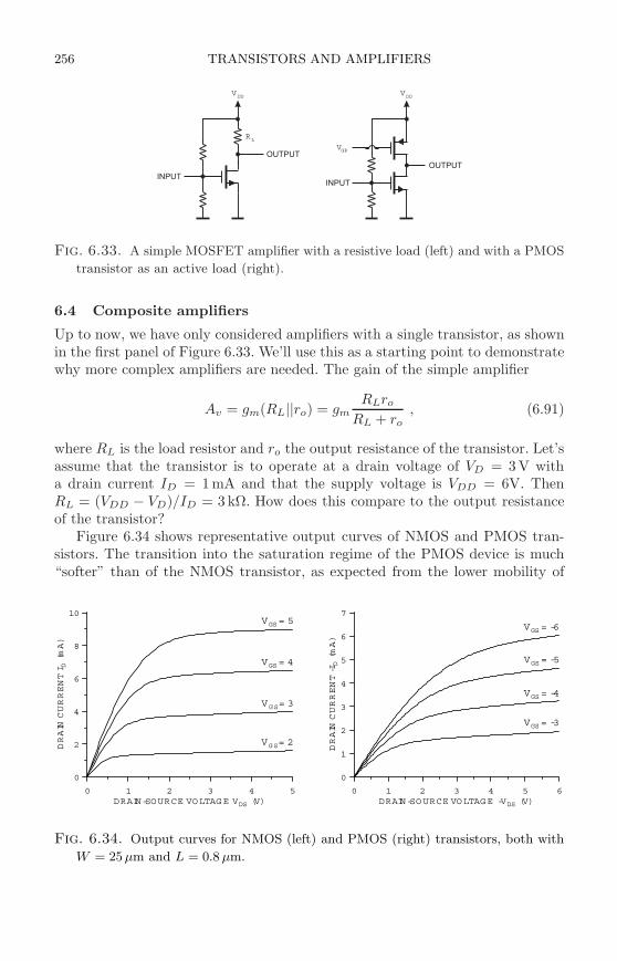
256 TRANSISTORS AND AMPLIFIERS
V V
V
R
DD DD
GP
L
OUTPUT
OUTPUT
INPUTINPUT
Fig. 6.33. A simple MOSFET amplifier with a resistive load (left) and with a PMOS
transistor as an active load (right).
6.4 Composite amplifiers
Up to now, we have only considered amplifiers with a single transistor, as shownin the first panel of Figure 6.33. We’ll use this as a starting point to demonstratewhy more complex amplifiers are needed. The gain of the simple amplifier
Av = gm(RL||ro) = gmRLro
RL + ro, (6.91)
where RL is the load resistor and ro the output resistance of the transistor. Let’sassume that the transistor is to operate at a drain voltage of VD = 3 V witha drain current ID = 1 mA and that the supply voltage is VDD = 6V. ThenRL = (VDD − VD)/ID = 3 kΩ. How does this compare to the output resistanceof the transistor?
Figure 6.34 shows representative output curves of NMOS and PMOS tran-sistors. The transition into the saturation regime of the PMOS device is much“softer” than of the NMOS transistor, as expected from the lower mobility of
0 1 2 3 4 5DRAIN-SOURCE VOLTAGE VDS (V)
0
2
4
6
8
10
DRAIN
CURRENTI D
(mA)
VGS= 2
VGS= 3
VGS= 4
0 1 2 3 4 5 6DRAIN-SOURCE VOLTAGE -VDS (V)
0
1
2
3
4
5
6
7
DRAIN
CURRENT-ID(mA)
VGS= -3
VGS= -4
VGS= -5
VGS= -6VGS= 5
Fig. 6.34. Output curves for NMOS (left) and PMOS (right) transistors, both with
W = 25 µm and L = 0.8 µm.
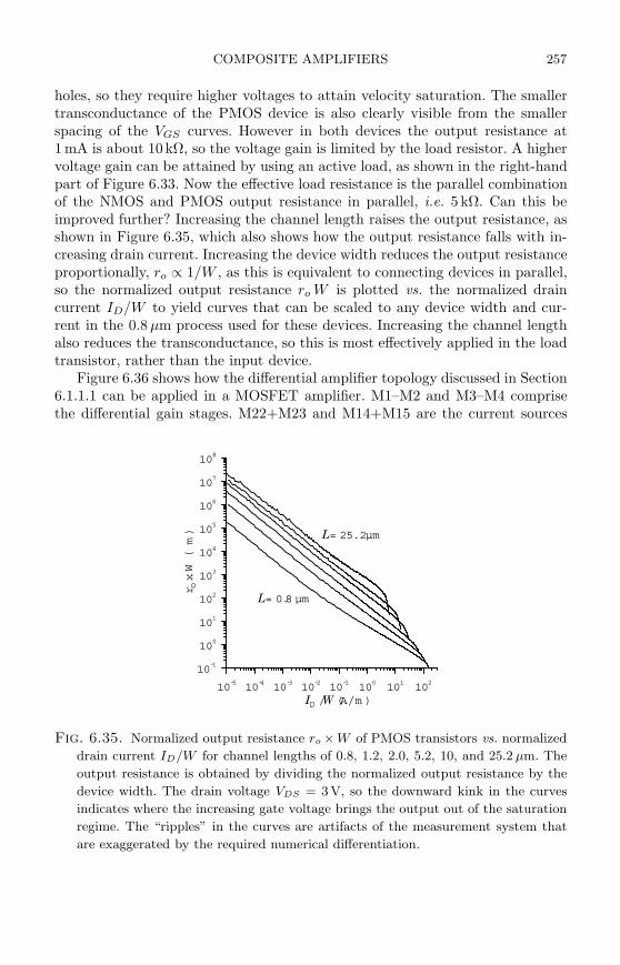
COMPOSITE AMPLIFIERS 257
holes, so they require higher voltages to attain velocity saturation. The smallertransconductance of the PMOS device is also clearly visible from the smallerspacing of the VGS curves. However in both devices the output resistance at1 mA is about 10 kΩ, so the voltage gain is limited by the load resistor. A highervoltage gain can be attained by using an active load, as shown in the right-handpart of Figure 6.33. Now the effective load resistance is the parallel combinationof the NMOS and PMOS output resistance in parallel, i.e. 5 kΩ. Can this beimproved further? Increasing the channel length raises the output resistance, asshown in Figure 6.35, which also shows how the output resistance falls with in-creasing drain current. Increasing the device width reduces the output resistanceproportionally, ro ∝ 1/W , as this is equivalent to connecting devices in parallel,so the normalized output resistance ro W is plotted vs. the normalized draincurrent ID/W to yield curves that can be scaled to any device width and cur-rent in the 0.8 µm process used for these devices. Increasing the channel lengthalso reduces the transconductance, so this is most effectively applied in the loadtransistor, rather than the input device.
Figure 6.36 shows how the differential amplifier topology discussed in Section6.1.1.1 can be applied in a MOSFET amplifier. M1–M2 and M3–M4 comprisethe differential gain stages. M22+M23 and M14+M15 are the current sources
10-5
10-4
10-3
10-2
10-1
100
101
102
ID /W (A/m )
10-1
100
101
102
103
104
105
106
107
108
r oxW(m)
L= 0.8 µm
L= 25.2 µm
Fig. 6.35. Normalized output resistance ro ×W of PMOS transistors vs. normalized
drain current ID/W for channel lengths of 0.8, 1.2, 2.0, 5.2, 10, and 25.2 µm. The
output resistance is obtained by dividing the normalized output resistance by the
device width. The drain voltage VDS = 3 V, so the downward kink in the curves
indicates where the increasing gate voltage brings the output out of the saturation
regime. The “ripples” in the curves are artifacts of the measurement system that
are exaggerated by the required numerical differentiation.

258 TRANSISTORS AND AMPLIFIERS
( )W/L
( )W/L
( )W/L
( )W/L
( )W/L
( )W/L
( )W/L
( )W/L
( )W/L
( )W/L
P
N
P
N
P
N
P
N
P
N
Vbias
v
v
i
o
M1
M12M11
M22M21
M14
M24
M3
M2
M13
M23
M15
M25
M4
M10
VDD
Fig. 6.36. A differential amplifier cascade implemented in CMOS technology. The
input signal is applied to M1–M2 and the output taken from M3–M4.
that set the standing current for the NMOS and PMOS differential pairs. M12,M13 and M24, M25 are the respective loads. M10, M11, and M21 establish thebias voltages for the current sources and loads.
The bias circuit demonstrates current mirroring, a powerful technique inmatching or scaling the operating currents of different stages. In the first gainstage the total currents through M12+M13 and M22+M23 must be equal. Thechain M11–M10–M21 is designed so that the current flowing through it is I0/2,which sets the appropriate gate–source voltages at M11 and M21. The gate–source voltage of M21 is transferred to M22 and M23, all of which have the samegeometry, so the gate voltage will establish the same current flow in each transis-tor, i.e. the current is “mirrored” from M21 to M22 and M23. Correspondingly,the gate–source voltage of M11 is transferred to the load transistors M12 andM13. The current source uses paralleled transistors M22 and M23 to establishthe total current I0, whereas the current flowing through the load transistorsM12 and M13 is I0/2. The second stage devices M14–M15 and M24–M25 are bi-ased correspondingly. In principle, the current sources M14+M15 and M22+M23could each be one transistor with twice the width, but since edge effects can beimportant, it is safest to use multiple transistors with the same geometry. Thebias transistor M10 establishes the appropriate voltage drop between M11 andM21 to match the drain–source voltage of the gain stages.
As described in Section 6.1.1.1 this circuit is insensitive to changes in thesupply voltage VDD and also to common mode components at the amplifierinputs (“common mode rejection”). The cascade of NMOS and PMOS stagesalso allows the quiescent level at the output to match the input.
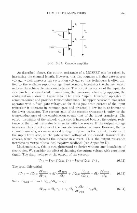
COMPOSITE AMPLIFIERS 259
V
V
V
V
V
I
I
G2
GS 1
GS 2
DS 1
DS 2
D
D
INPUT
Fig. 6.37. Cascode amplifier.
As described above, the output resistance of a MOSFET can be raised byincreasing the channel length. However, this also requires a higher gate–sourcevoltage, which increases the saturation voltage, so this techniques is often lim-ited by the available supply voltage. Furthermore, increasing the channel lengthreduces the achievable transconductance. The output resistance of the input de-vice can be increased while maintaining the transconductance by applying theconfiguration shown in Figure 6.37. The lower “input” transistor operates incommon-source and provides transconductance. The upper “cascode” transistoroperates with a fixed gate voltage, so for the signal drain current of the inputtransistor it operates in common-gate and presents a low input resistance tothe lower transistor. The current gain of the cascode transistor is unity, so thetransconductance of the combination equals that of the input transistor. Theoutput resistance of the cascode transistor is increased because the output resis-tance of the input transistor is in series with the source. If the output voltageincreases, the current draw of the cascode transistor increases. However, the in-creased current gives an increased voltage drop across the output resistance ofthe input transistor, so the gate–source voltage of the cascode transistor de-creases, which counteracts the increase in current. Thus, the output resistanceincreases by virtue of this local negative feedback (see Appendix D).
Mathematically, this is straightforward to derive without any knowledge ofelectronics. We consider the effect of changing the output voltage with zero inputsignal. The drain voltage at the output of the cascode
VDS = VDS1(VGS1, ID) + VDS2(VGS2, ID) . (6.92)
The total differential
dVDS = dVGS1dVDS1
dVGS1+ dID
dVDS1
dID+ dVGS2
dVDS2
dVGS2+ dID
dVDS2
dID. (6.93)
Since dVGS1 ≡ 0 and dVDS/dID = ro,
dVDS = dIDro1 + ro1dIDro2dID
dVGS2+ ro2dID (6.94)
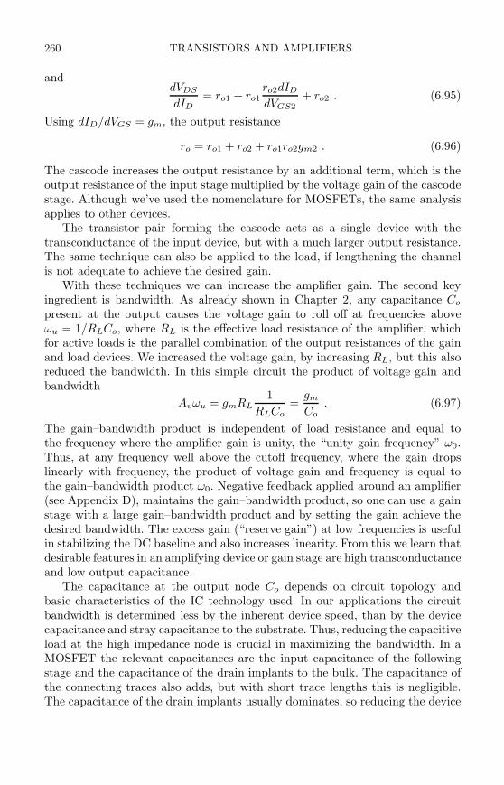
260 TRANSISTORS AND AMPLIFIERS
anddVDS
dID= ro1 + ro1
ro2dID
dVGS2+ ro2 . (6.95)
Using dID/dVGS = gm, the output resistance
ro = ro1 + ro2 + ro1ro2gm2 . (6.96)
The cascode increases the output resistance by an additional term, which is theoutput resistance of the input stage multiplied by the voltage gain of the cascodestage. Although we’ve used the nomenclature for MOSFETs, the same analysisapplies to other devices.
The transistor pair forming the cascode acts as a single device with thetransconductance of the input device, but with a much larger output resistance.The same technique can also be applied to the load, if lengthening the channelis not adequate to achieve the desired gain.
With these techniques we can increase the amplifier gain. The second keyingredient is bandwidth. As already shown in Chapter 2, any capacitance Co
present at the output causes the voltage gain to roll off at frequencies aboveωu = 1/RLCo, where RL is the effective load resistance of the amplifier, whichfor active loads is the parallel combination of the output resistances of the gainand load devices. We increased the voltage gain, by increasing RL, but this alsoreduced the bandwidth. In this simple circuit the product of voltage gain andbandwidth
Avωu = gmRL1
RLCo=
gm
Co. (6.97)
The gain–bandwidth product is independent of load resistance and equal tothe frequency where the amplifier gain is unity, the “unity gain frequency” ω0.Thus, at any frequency well above the cutoff frequency, where the gain dropslinearly with frequency, the product of voltage gain and frequency is equal tothe gain–bandwidth product ω0. Negative feedback applied around an amplifier(see Appendix D), maintains the gain–bandwidth product, so one can use a gainstage with a large gain–bandwidth product and by setting the gain achieve thedesired bandwidth. The excess gain (“reserve gain”) at low frequencies is usefulin stabilizing the DC baseline and also increases linearity. From this we learn thatdesirable features in an amplifying device or gain stage are high transconductanceand low output capacitance.
The capacitance at the output node Co depends on circuit topology andbasic characteristics of the IC technology used. In our applications the circuitbandwidth is determined less by the inherent device speed, than by the devicecapacitance and stray capacitance to the substrate. Thus, reducing the capacitiveload at the high impedance node is crucial in maximizing the bandwidth. In aMOSFET the relevant capacitances are the input capacitance of the followingstage and the capacitance of the drain implants to the bulk. The capacitance ofthe connecting traces also adds, but with short trace lengths this is negligible.The capacitance of the drain implants usually dominates, so reducing the device
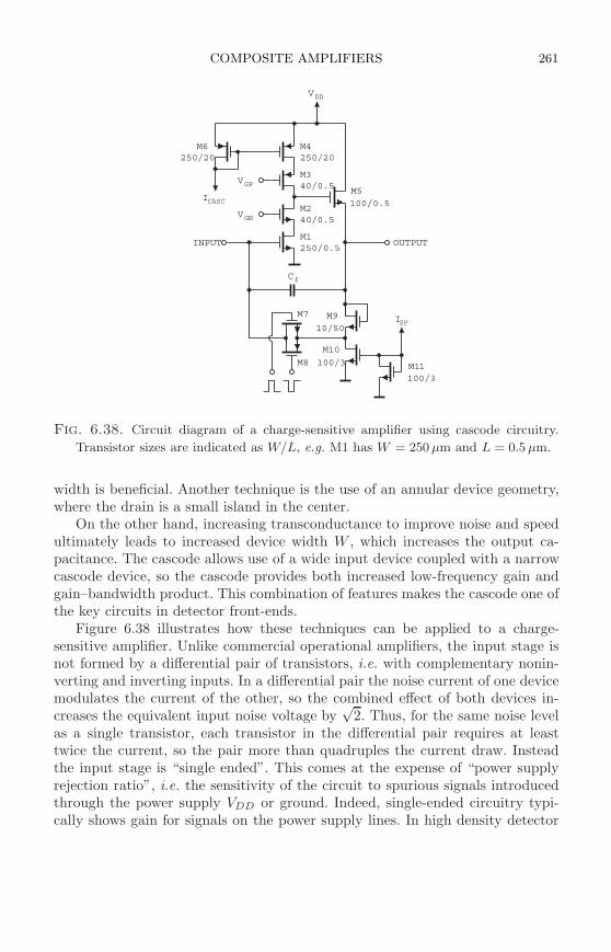
COMPOSITE AMPLIFIERS 261
OUTPUTINPUT
V
V
I
V
C
I
DD
GP
CASC
GN
f
SF
M1
M7
M10
M11M8
M2
M5
M3
M4M6
M9
250/20
40/0.5
40/0.5
250/0.5
250/20
10/50
100/0.5
100/3
100/3
Fig. 6.38. Circuit diagram of a charge-sensitive amplifier using cascode circuitry.
Transistor sizes are indicated as W/L, e.g. M1 has W = 250 µm and L = 0.5 µm.
width is beneficial. Another technique is the use of an annular device geometry,where the drain is a small island in the center.
On the other hand, increasing transconductance to improve noise and speedultimately leads to increased device width W , which increases the output ca-pacitance. The cascode allows use of a wide input device coupled with a narrowcascode device, so the cascode provides both increased low-frequency gain andgain–bandwidth product. This combination of features makes the cascode one ofthe key circuits in detector front-ends.
Figure 6.38 illustrates how these techniques can be applied to a charge-sensitive amplifier. Unlike commercial operational amplifiers, the input stage isnot formed by a differential pair of transistors, i.e. with complementary nonin-verting and inverting inputs. In a differential pair the noise current of one devicemodulates the current of the other, so the combined effect of both devices in-creases the equivalent input noise voltage by
√2. Thus, for the same noise level
as a single transistor, each transistor in the differential pair requires at leasttwice the current, so the pair more than quadruples the current draw. Insteadthe input stage is “single ended”. This comes at the expense of “power supplyrejection ratio”, i.e. the sensitivity of the circuit to spurious signals introducedthrough the power supply VDD or ground. Indeed, single-ended circuitry typi-cally shows gain for signals on the power supply lines. In high density detector
262 TRANSISTORS AND AMPLIFIERS
systems the need to reduce power tends to prevail over the robustness of fullydifferential circuitry.
Cascodes are used both in the gain and load portions. M1 and M2 comprisethe transconductance stage and M3 and M4 the load. M1 is sized to providethe required transconductance for the desired noise. M2 and M3 have a substan-tially smaller width to reduce the capacitance at the high impedance node. Thetransconductance of M4 is not important, but it should have a large output re-sistance (see eqn 6.96). To avoid additional capacitive loading by the subsequentstage, the output is fed through a source follower M5. The high input impedanceof the source follower also maintains the voltage gain independent of load. Thesource follower also provides current drive capability.
The detector is capacitively fed back through Cf , but DC feedback must alsobe provided, both to set the DC operating point and to discharge the feedbackcapacitor. This is achieved by a CMOS pair M7 and M8 in parallel with thefeedback capacitor. When DC biased the transistors act as resistors to contin-uously discharge the feedback capacitor and provide DC feedback to maintainthe DC level at the amplifier output. This can also be accomplished by onlyone transistor. The second transistor is important in the second operating mode,which uses pulsed feedback. Here the reset transistors are driven by a short pulse,which discharges the feedback capacitor and also charges the amplifier input tothe proper potential. A transistor pair is used to cancel the charge injectionthrough the gate–channel capacitance. The NMOS and PMOS transistors aredriven with pulses of opposite polarity. The device geometries of M7 and M8 aresmall to reduce the gate–channel capacitance, but sized individually to matchtheir gate capacitances and cancel the injected charge.
Transistor M9 shifts the output level to set the voltage at the juncture ofM2 and M3 to approximately VDD/2. When the feedback switch is closed thisvoltage is VGS(M1)+VDS(M9)+VGS(M5). Voltages VGN and VGP set the drainvoltages of M1 and M4.
Another detail is the current mirror M6 that sets the operating current. Sinceboth the noise and speed of the amplifier are set by the transconductance of theinput device, and the transconductance is set primarily by current, controllingthe current is crucial. The current mirror allows the cascode current to be set byan external current, which is not subject to device parameter variations on thechip. This is especially useful in circuits subject to radiation damage, which willbe discussed in the next chapter. Setting the current may be as simple as con-necting a resistor from the ICASC port to ground. Since the voltage drop acrossthe resistor is typically several times than the gate–source voltage of the currentmirror, the dependence of ICASC to transistor threshold voltage variations isreduced.
To first order the gain–bandwidth product f0 and the feedback network setthe upper cutoff frequency fu = f0/(1 + Cd/Cf ) and thus the rise time constantτ = 1/(2πfu). However, as discussed briefly in Chapter 2 and treated in Ap-pendix D, in a feedback amplifier the phase shift is also critical. At frequencies
COMPOSITE AMPLIFIERS 263
well below the cutoff frequency the phase shift is zero (or in an inverting ampli-fier 180). At the cutoff frequency the complex load incurs an additional 45 andat frequencies well above the cutoff frequencies the load is imaginary (i.e. purelycapacitive) and the additional phase shift is constant at 90. If these were theonly phase shifts, the feedback loop would be unconditionally stable. However,additional time constants are introduced by the additional devices that affectthe signal path.
This amplifier topology can provide a gain–bandwidth product of about1 GHz with < 1 mW power dissipation. The dominant pole set is by the transcon-ductance of M1 and the total capacitance at the cascode output. However, addi-tional time constants are introduced at the juncture of M1 and M2, which setsthe minimum width of M2, and in the source follower. In the design shown inFigure 6.38 the second pole is at several hundred MHz, so the reset path must in-clude some attenuation (provided by M9) to prevent self-oscillation during reset,as the reset switch establishes unity gain.
This illustrates why even a “single stage” amplifier can be limited to closedloop bandwidths substantially smaller than the unity gain frequency. It alsoshows that if feedback is to be applied around a cascade of amplifiers, the cutofffrequencies of the individual amplifiers cannot be the same. The overall frequencyresponse of the cascade must be dominated by one amplifier and the cutoff fre-quencies of the other stages must be well above the frequency where the loop gainis unity. Kipnis, Spieler, and Collins (1994) describe another variant of a cascodepreamplifier using bipolar transistors showing the gain and phase response.
The frequency break points are usually called “poles”, as feedback systemsare often analyzed using Laplace transforms, where the time constants appear aspoles in complex frequency space. An ideal amplifier with just one time constanthas a “single pole response”. Many commercially available operational amplifiersare made unconditionally stable for all gains by deliberately reducing the gain–bandwidth product at the first cutoff frequency such that all higher poles arewell above the unity gain frequency. However, the freedom in design comes atthe expense of bandwidth.
The loop gain in normal operation of the circuit in Figure 6.38 is
AvL = Av0Cf
Cd + Cf, (6.98)
where Cd is the detector capacitance and Av0 is the open loop gain of the am-plifier. In Figure 6.38 this is the voltage gain measured between the input andoutput in the absence of feedback. When the reset switch M7–M8 is closed,the impedance in the feedback path is much smaller, so the loop gain moves toan unstable regime. To compensate for this the output signal is connected tothe reset switch through the voltage divider M19–M10. This scheme allows ahigher bandwidth (faster response time) for signal acquisition than an amplifierdesigned for unconditional stability under all feedback conditions.
264 TRANSISTORS AND AMPLIFIERS
OUTPUT
INPUT
V
V
V
V
V
C
DD
GN 1
GP
GN 2
GN 3
f
M2
M4
M3
M9
M5
M6
M1
OUTPUT
INPUT
V
V
V
V
V
C
DD
GP 1
GP 2
GN 1
GN 2
f
M1 M3
M4
M9
M5
M6
M2
Fig. 6.39. The folded cascode implemented with an NMOS input (left) and a PMOS
input transistor (right). The arrows show the signal current path of the input tran-
sistor M1. The bulk of M1’s standing current is provided by M2.
A popular variant of the cascode amplifier is the “folded” cascode shownin Figure 6.39. This circuit avoids two conflicts inherent to the linear cascode.As the input transistor determines the equivalent noise, it must operate at arelatively high current. For a high output resistance, however, low current is ad-vantageous. The folded cascode addresses these requirements by separating theDC and signal current paths. Since M3 presents a low input resistance, the out-put resistance of M2 is sufficiently high without an additional cascode transistor,so that practically all of M1’s signal current flows into the low input resistancepresented by M3. Since only a fraction of M1’s standing current flows thoughthe load transistor M4, the desired high load resistance can be achieved with-out a cascode load, further reducing the total voltage requirements. The foldedcascode can be implemented with either NMOS or PMOS inputs. The latterprovides lower 1/f noise, which in some applications outweighs the somewhatinferior transconductance of the PMOS input transistor. Some commonly usedimplementations of the folded cascode are quite prone to spurious pickup andcross-talk. This will be discussed in Chapter 9.
Although CMOS was used in these examples, similar circuits can be imple-mented with bipolar transistors or combinations of bipolar and MOS devices(using bi-CMOS integrated circuit processes, for example). Indeed, the basicconsiderations and circuit derivations apply to any transconductance device, beit a bipolar transistor, JFET, MOSFET or vacuum tube. Bipolar transistorsprovide higher transconductance and generally allow lower power dissipation inamplifiers, whereas CMOS provides added flexibility in the choice of device ge-ometry. CMOS also provides higher circuit density and in mixed analog-digitalsystems the advantages of a full CMOS implementation on a single chip usuallyoutweigh transconductance considerations.
OVERALL NOISE OF A DETECTOR MODULE 265
80 120 160 200 240 280 320COLLECTOR CURRENT (µA)
1200
1300
1400
1500
1600
EQUIVALENTNOISECHARGE(e)
Fig. 6.40. Measured noise vs. collector current of a strip detector module using a
bipolar transistor front-end and a 12 cm long strip sensor. The peaking time at the
output of the pulse shaper is about 25 ns.
This discussion was not meant to be an exhaustive treatment of amplifierdesign, but is intended to provide a glimpse of the rationale behind some commoncircuits. Many other circuit techniques and more detailed analyses are needed toimplement a full system and a vast body of literature is available to delve moredeeply into the subject.
6.5 Overall noise of a detector module
Figure 6.40 shows the measured noise of a complete detector module vs. col-lector current of the bipolar transistor input stage. The noise decreases withcollector current and reaches a minimum at about 250 µA, which was the designvalue. The circuit was not designed to operate at higher currents than 300 µA,so the noise could not be measured beyond the minimum. The simulated noiselevels are 1460e at 150µA and 1230 e at 300µA, in good agreement with themeasurements.
Although the first amplifying device should dominate the system’s electronicnoise, many other contributions add up to increase the overall noise. The in-dividual contributions may be small, but there are many, so that in practicethe overall noise level is 10 – 20% higher than for the input device alone. Table6.1 shows a representative breakdown for a strip detector system with a bipolartransistor front-end.
The input transistor contributes only 50 – 60% of the total noise, with thecollector and base current contributing about 80% of that and the base resistancethe remainder. Substantial contributions come from the neighbor amplifiers andstrips, as was discussed in Chapter 3. The thermal noise of the strip resistancecan be reduced by connecting the amplifier at the midpoints of the strips, ratherthan at the ends. Contributions from other components in the preamplifier circuit
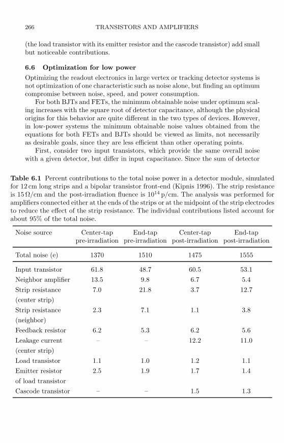
266 TRANSISTORS AND AMPLIFIERS
(the load transistor with its emitter resistor and the cascode transistor) add smallbut noticeable contributions.
6.6 Optimization for low power
Optimizing the readout electronics in large vertex or tracking detector systems isnot optimization of one characteristic such as noise alone, but finding an optimumcompromise between noise, speed, and power consumption.
For both BJTs and FETs, the minimum obtainable noise under optimum scal-ing increases with the square root of detector capacitance, although the physicalorigins for this behavior are quite different in the two types of devices. However,in low-power systems the minimum obtainable noise values obtained from theequations for both FETs and BJTs should be viewed as limits, not necessarilyas desirable goals, since they are less efficient than other operating points.
First, consider two input transistors, which provide the same overall noisewith a given detector, but differ in input capacitance. Since the sum of detector
Table 6.1 Percent contributions to the total noise power in a detector module, simulatedfor 12 cm long strips and a bipolar transistor front-end (Kipnis 1996). The strip resistanceis 15 Ω/cm and the post-irradiation fluence is 1014 p/cm. The analysis was performed foramplifiers connected either at the ends of the strips or at the midpoint of the strip electrodesto reduce the effect of the strip resistance. The individual contributions listed account forabout 95% of the total noise.
Noise source Center-tap End-tap Center-tap End-tappre-irradiation pre-irradiation post-irradiation post-irradiation
Total noise (e) 1370 1510 1475 1555
Input transistor 61.8 48.7 60.5 53.1
Neighbor amplifier 13.5 9.8 6.7 5.4
Strip resistance 7.0 21.8 3.7 12.7
(center strip)
Strip resistance 2.3 7.1 1.1 3.8
(neighbor)
Feedback resistor 6.2 5.3 6.2 5.6
Leakage current – – 12.2 11.0
(center strip)
Load transistor 1.1 1.0 1.2 1.1
Emitter resistor 2.5 1.9 1.7 1.4
of load transistor
Cascode transistor – – 1.5 1.3
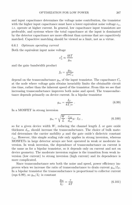
OPTIMIZATION FOR LOW POWER 267
and input capacitance determines the voltage noise contribution, the transistorwith the higher input capacitance must have a lower equivalent noise voltage en,i.e. operate at higher current. In general, low capacitance input transistors arepreferable, and systems where the total capacitance at the input is dominatedby the detector capacitance are more efficient than systems that are capacitivelymatched. Capacitive matching should be viewed as a limit, not as a virtue.
6.6.1 Optimum operating current
Both the equivalent input noise voltage
e2n ≈ 4kT
gm
and the gain–bandwidth product
f0 =gm
2πCo
depend on the transconductance gm of the input transistor. The capacitance Co
at the node where voltage gain obtains invariably limits the obtainable circuitrise time, rather than the inherent speed of the transistor. From this we see thatincreasing transconductance improves both noise and speed. The transconduc-tance depends primarily on device current. In a bipolar transistor
gm =IC
kT/e. (6.99)
In a MOSFET in strong inversion
gm =
√
W
L· εox
doxµ · ID , (6.100)
so for a given device width W , reducing the channel length L or gate oxidethickness dox should increase the transconductance. The choice of bulk mate-rial determines the carrier mobility µ and the gate oxide’s dielectric constantεox. However, this simple scaling rule only applies in strong inversion, whereasMOSFETs in large detector arrays are best operated in weak or moderate in-version. In weak inversion, the dependence of transconductance on current isthe same as for a bipolar transistor, so it depends only on current and not ondevice geometry. The moderate inversion regime is the transition from weak in-version (low current) to strong inversion (high current) and its dependence ismore complicated.
Since transconductance sets both the noise and speed, power efficiency im-proves when we increase the ratio of transconductance to drain current gm/ID .In a bipolar transistor the transconductance is proportional to collector current(eqn 6.99), so gm/IC is constant
gm
IC=
e
kT(6.101)
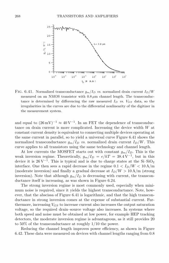
268 TRANSISTORS AND AMPLIFIERS
10-4
10-3
10-2
10-1
100
101
102
103
ID /W (A/m )
0
5
10
15
20
25
gm/I D(V
-1)
L= 0.8 µm
Fig. 6.41. Normalized transconductance gm/ID vs. normalized drain current ID/W
measured on an NMOS transistor with 0.8 µm channel length. The transconduc-
tance is determined by differencing the raw measured ID vs. VGS data, so the
irregularities in the curves are due to the differential nonlinearity of the digitizer in
the measurement system.
and equal to (26 mV)−1 ≈ 40 V−1. In an FET the dependence of transconduc-tance on drain current is more complicated. Increasing the device width W atconstant current density is equivalent to connecting multiple devices operating atthe same current in parallel, so to yield a universal curve Figure 6.41 shows thenormalized transconductance gm/ID vs. normalized drain current ID/W . Thiscurve applies to all transistors using the same technology and channel length.
At low currents the MOSFET starts out with constant gm/ID. This is theweak inversion regime. Theoretically, gm/ID = e/kT = 38.4 V−1, but in thisdevice it is 26 V−1. This is typical and is due to charge states at the Si–SiO2
interface. One then sees a rapid decrease in the regime 0.1 < ID/W < 10 A/m(moderate inversion) and finally a gradual decrease at ID/W > 10 A/m (stronginversion). Note that although gm/ID is decreasing with current, the transcon-ductance itself is increasing, as was shown in Figure 6.24.
The strong inversion regime is most commonly used, especially when mini-mum noise is required, since it yields the highest transconductance. Note, how-ever, that the abscissa of Figure 6.41 is logarithmic, and that the high transcon-ductance in strong inversion comes at the expense of substantial current. Fur-thermore, increasing VGS to increase current also increases the output saturationvoltage, so the required drain–source voltage also increases. In systems whereboth speed and noise must be obtained at low power, for example HEP trackingdetectors, the moderate inversion regime is advantageous, as it still provides 20to 50% of the transconductance at roughly 1/10 the power.
Reducing the channel length improves power efficiency, as shown in Figure6.42. These data were measured on devices with channel lengths ranging from 0.8
OPTIMIZATION FOR LOW POWER 269
10-4
10-3
10-2
10-1
100
101
102
103
ID /W (A/m )
0
5
10
15
20
25
gm/I D(V
-1)
L= 0.8 µm
L= 25.2 µm
Fig. 6.42. Normalized transconductance gm/ID vs. normalized drain current ID/W
for channel lengths of 0.8, 1.2, 2.0, 5.2, 10.0, and 25.2 µm. All devices were fabricated
on the same die in a 0.8 µm CMOS process. The irregularities in the curves are due
to the differential nonlinearity of the digitizer in the measurement system.
to 25.2 µm, all on the same chip and fabricated in a 0.8 µm process. For example,the 0.8 µm channel length device shows gm/ID = 24 at ID/W = 10−3 andgm/ID ≈ 1 at ID/W = 100. The transition from weak to strong inversion shiftsto higher currents as the channel length is reduced. At ID/W = 0.1 the 0.8 µmlong device yields gm/ID = 21, whereas 25 µm long devices yield gm/ID = 6.Thus, reducing the channel length allows more efficient circuitry, although notas predicted by the strong inversion formula.
The best power efficiency obtains at the highest normalized transconductancegm/ID that will provide the desired noise level. Uniquely associated with thisvalue of gm/ID is a current density (ID/W )gm/ID
, which for a given technologydepends on the channel length. While keeping the current density constant, onecan adjust the width to change the transconductance. As the width is changed thedrain current ID = W ·(ID/W )gm/ID
changes proportionally. This value of draincurrent sets the transconductance gm(W ) = W · (ID/W )gm/ID
(gm/ID)selected.Thus, both the drain current and the transconductance scale proportionally towidth, as does the FET’s input capacitance. As the width is increased the equiv-alent noise charge decreases until the input capacitance equals the sensor capac-itance. With further increases in width the increase in capacitance outweighs thedecrease in noise voltage, so the noise charge increases. If the minimum noise istoo high, one chooses a lower value of gm/ID, which will achieve a given transcon-ductance at a smaller device width, so capacitive matching will occur at a highertransconductance. Thus the minimum noise will be lower, albeit at the expenseof power dissipation. This procedure is illustrated in Figure 6.43.
For example, assume that the desired noise level is 1000 e. A normalizedtransconductance gm/ID = 24 (weak inversion) allows a minimum noise of 1400 e
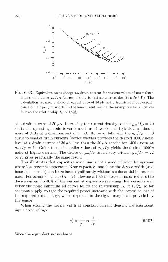
270 TRANSISTORS AND AMPLIFIERS
10-7
10-6
10-5
10-4
10-3
10-2
10-1
100
101
ID (A)
101
102
103
104
Qn(e)
gm /ID = 24
23
20
1612
84
2 1
Fig. 6.43. Equivalent noise charge vs. drain current for various values of normalized
transconductance gm/ID (corresponding to unique current densities ID/W ). The
calculation assumes a detector capacitance of 10 pF and a transistor input capaci-
tance of 1 fF per µm width. In the low-current regime the asymptote for all curves
follows the relationship ID ∝ 1/Q2n.
at a drain current of 50 µA. Increasing the current density so that gm/ID = 20shifts the operating mode towards moderate inversion and yields a minimumnoise of 340 e at a drain current of 1 mA. However, following the gm/ID = 20curve to smaller drain currents (device widths) provides the desired 1000 e noiselevel at a drain current of 30 µA, less than the 50 µA needed for 1400 e noise atgm/ID = 24. Going to much smaller values of gm/ID yields the desired 1000 enoise at higher currents. The choice of gm/ID is not very critical; gm/ID = 22or 23 gives practically the same result.
This illustrates that capacitive matching is not a good criterion for systemswhere low power is important. Near capacitive matching the device width (andhence the current) can be reduced significantly without a substantial increase innoise. For example, at gm/ID = 24 allowing a 10% increase in noise reduces thedevice current to 40% of the current at capacitive matching. For currents wellbelow the noise minimum all curves follow the relationship ID ∝ 1/Q2
n, so forconstant supply voltage the required power increases with the inverse square ofthe required noise charge, which depends on the signal magnitude provided bythe sensor.
When scaling the device width at constant current density, the equivalentinput noise voltage
e2n ∝ 1
gm∝ 1
ID. (6.102)
Since the equivalent noise charge
OPTIMIZATION FOR LOW POWER 271
Q2n ∝ e2
nC2 ∝ C2
ID, (6.103)
when operating well below capacitive matching, the required power for a givennoise level increases with the square of sensor capacitance,
PD ∝ ID ∝ C2 . (6.104)
A similar result obtains for bipolar transistors. The most efficient operatingregime with respect to power is at a current well below the current needed forminimum noise
IC =kT
eCtot
√
βDC
√
Fv
Fi
1
TS. (6.105)
In this regime the noise is dominated by voltage noise, so
Q2n ≈ 2(kT )2
eICC2 Fv
TS(6.106)
and for a given noise level C2/IC is constant, so the required power
P ∝ IC ∝ C2 . (6.107)
In this form of optimum scaling the required power in the input device scales withthe square of capacitance at the input. The required power also increases withthe square of the desired signal-to-noise ratio. Even when the required noise levelis close to the minimum noise, one can operate well below the optimum current,as the noise minimum is rather shallow.
These scaling rules represent optimum scaling, where the device input capac-itance is negligible, i.e. well below capacitive matching. For comparison, fromFigure 6.43 a 2000-fold increase in current reduces the minimum noise at ca-pacitive matching from 1400 to 50 e, whereas optimum scaling requires that thecurrent increase only 800-fold. The difference is due to the penalty incurred bythe device capacitance.
As illustrated above, the optimization is iterative and usually involves severalcomponents, but basically one starts with a circuit topology and chooses a nor-malized drain current ID/W that provides an adequate gain–bandwidth product.For example, in Figure 6.38 this involves setting the ratio of device widths in thecascode. If the capacitive load at the output node is dominated by device widths,then scaling all widths while scaling the current simultaneously to maintain thecurrent density ID/W , will maintain the amplifier’s gain–bandwidth productgm/Co.
6.6.2 Technology improvements
To what extent do improvements in device technology improve amplifier per-formance? Can we simply rely on Moore’s Law to meet future needs? There is
272 TRANSISTORS AND AMPLIFIERS
a widespread tendency to expect the miracles of modern technology to makepossible what is impossible today.
The preceding section underscores the importance of transconductance andits relationship to power dissipation. Low electronic noise levels require suffi-cient transconductance coupled with acceptable input capacitance. In addition,large detector arrays require that these parameters obtain at low power. Theserequirements militate against many novel technologies that appear to simplifyfabrication and reduce cost. Examples are amorphous silicon transistors or thinfilm transistors deposited by inkjet printing. All of these devices suffer from lowmobilities and, hence, low transconductance. Nanotechnology offers the potentialof very small devices, and the notion of “self-assembly” will appeal to anyone whohas constructed a complex detector, but nanotransistors will require nanosen-sors to reduce capacitance to match the small transconductance. Nanometer thinsensors in trackers yield correspondingly small signals, which require lower noiseand drive up front-end power. These novel devices will make inroads as switchingdevices, but their applicability to low-noise analog circuits is dubious. For theapplications considered here crystalline devices appear to offer the most realis-tic prospects for technological improvements. The basic scaling rules discussedabove still apply, but we seek improvements in the normalized transconductancegm/I .
The transconductance of MOSFETs in weak inversion depends on currentalone, so the parameter that can be improved is input capacitance. If smaller fea-ture sizes push the weak inversion regime to higher current densities, a narrowerdevice will provide the required transconductance at a lower input capacitance.However, a thinner gate oxide increases the capacitance per unit area, so thereduction in width must be balanced against the normalized input capacitanceCi/W ∝ L/dox.
For MOSFETs in strong inversion
gm√ID
=
√
W
L· εox
doxµ , (6.108)
so high-density processes with shorter channel lengths L and thinner gate oxideswill provide higher transconductance at a given current. Furthermore, the mod-erate inversion regime occurs at more favorable currents, as shown in Figure 6.42.However, it is not clear that moving to yet smaller channel lengths than shownin Figure 6.42 will provide similar benefits in the moderate inversion regime thatis most interesting for low-noise amplifiers. Figure 6.44 compares measured datafor NMOS devices with L = 0.8 and 0.3 µm channel lengths, fabricated in 0.8and 0.25 µm CMOS processes, respectively. In the higher density process thetransition from weak to moderate inversion occurs in the same current range asin the 0.8 µm MOSFET and the normalized transconductance in weak inversionis distinctly lower.
Why does the 0.3 µm channel length not show the expected improvement?Scaling to smaller feature size involves more than lateral scaling, i.e. resolution
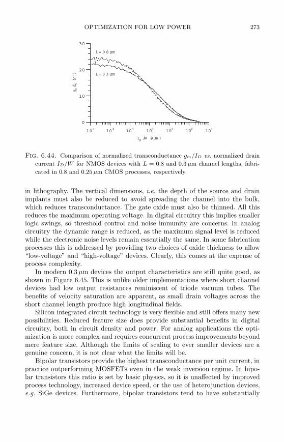
OPTIMIZATION FOR LOW POWER 273
10-3
10-2
10-1
100
101
102
103
ID /W (A/m )
0
10
20
30
gm/ID(V
-1) L= 0.3 µm
L= 0.8 µm
Fig. 6.44. Comparison of normalized transconductance gm/ID vs. normalized drain
current ID/W for NMOS devices with L = 0.8 and 0.3 µm channel lengths, fabri-
cated in 0.8 and 0.25 µm CMOS processes, respectively.
in lithography. The vertical dimensions, i.e. the depth of the source and drainimplants must also be reduced to avoid spreading the channel into the bulk,which reduces transconductance. The gate oxide must also be thinned. All thisreduces the maximum operating voltage. In digital circuitry this implies smallerlogic swings, so threshold control and noise immunity are concerns. In analogcircuitry the dynamic range is reduced, as the maximum signal level is reducedwhile the electronic noise levels remain essentially the same. In some fabricationprocesses this is addressed by providing two choices of oxide thickness to allow“low-voltage” and “high-voltage” devices. Clearly, this comes at the expense ofprocess complexity.
In modern 0.3 µm devices the output characteristics are still quite good, asshown in Figure 6.45. This is unlike older implementations where short channeldevices had low output resistances reminiscent of triode vacuum tubes. Thebenefits of velocity saturation are apparent, as small drain voltages across theshort channel length produce high longitudinal fields.
Silicon integrated circuit technology is very flexible and still offers many newpossibilities. Reduced feature size does provide substantial benefits in digitalcircuitry, both in circuit density and power. For analog applications the opti-mization is more complex and requires concurrent process improvements beyondmere feature size. Although the limits of scaling to ever smaller devices are agenuine concern, it is not clear what the limits will be.
Bipolar transistors provide the highest transconductance per unit current, inpractice outperforming MOSFETs even in the weak inversion regime. In bipo-lar transistors this ratio is set by basic physics, so it is unaffected by improvedprocess technology, increased device speed, or the use of heterojunction devices,e.g. SiGe devices. Furthermore, bipolar transistors tend to have substantially
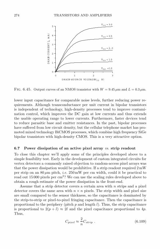
274 TRANSISTORS AND AMPLIFIERS
0 1 2 3
DRAIN-SOURCE VOLTAGE VD S (V)
0
1
2
3
4
5
DRAIN
CURRENTI D
(mA)
VG S = 1.0
VG S = 1.5
VG S = 2.0
VG S = 2.5
VG S = 3.0
Fig. 6.45. Output curves of an NMOS transistor with W = 9.45 µm and L = 0.3 µm.
lower input capacitance for comparable noise levels, further reducing power re-quirements. Although transconductance per unit current in bipolar transistorsis independent of technology, high-density processes tend to improve contami-nation control, which improves the DC gain at low currents and thus extendsthe usable operating range to lower currents. Furthermore, faster devices tendto reduce parasitic base and emitter resistances. In the past, bipolar processeshave suffered from low circuit density, but the cellular telephone market has pro-moted mixed technology BiCMOS processes, which combine high frequency SiGebipolar transistors with high-density CMOS. This is a very attractive option.
6.7 Power dissipation of an active pixel array vs. strip readout
To close this chapter we’ll apply some of the principles developed above to asimple feasibility test. Early in the development of custom integrated circuits forvertex detectors a commonly raised objection to random-access pixel arrays wasthat the power dissipation would be prohibitive. If a strip readout required 2mWper strip on an 80 µm pitch, i.e. 250mW per cm width, could it be practical toread out 15 000 pixels per cm2? We can use the scaling rules developed above toobtain a rough estimate of the power dissipation in the front-end.
Assume that a strip detector covers a certain area with n strips and a pixeldetector covers the same area with n × n pixels. The strip width and pixel sizeare small compared to the sensor thickness, so the capacitance is dominated bythe strip-to-strip or pixel-to-pixel fringing capacitance. Then the capacitance isproportional to the periphery (pitch p and length l). Thus, the strip capacitanceis proportional to 2(p + l) ≈ 2l and the pixel capacitance proportional to 4p.Thus,
Cpixel ≈2
nCstrip . (6.109)
REFERENCES 275
As discussed above, under optimal scaling the power dissipation of the readoutamplifier for a given noise level is proportional to the square of capacitanceP ∝ C2, so the power per pixel
Ppixel ≈4
n2Pstrip . (6.110)
Since there are n times as many pixels as strips, the power in all pixels’ front-ends
Ppixel,tot ≈4
nPstrip . (6.111)
From this we see that increasing the number of readout channels can reduce thetotal power dissipation.
The circuitry per cell does not consist of the amplifier alone, so a fixedpower P0 per cell must be added, bringing up the total power by n2P0, sothese savings are only realized in special cases. Nevertheless, this estimate showsthat power dissipation is not a fundamental hurdle in the implementation ofhighly segmented arrays. In practice, random addressable pixel arrays for high-luminosity colliders have been implemented with overall power densities (totalpower/detector area) comparable to strip detector systems.
References
Bardeen, J. and Brattain, W.H. (1948). The transistor, a semiconductor triode.Phys. Rev. 74 (1948) 230–231
Baker, R.J., Li, H.W. and Boyce, D.E. (1998). CMOS Circuit Design, Lay-out, and Simulation. IEEE Press, New York. ISBN 0-7803-3416-7, TK7871.99.M44B35 1997
Cooke, H.F. (1971). Microwave transistors: theory and design. Proc. IEEE 59/8(1971) 1163–1181
Grove, A.S. (1967). Physics and Technology of Semiconductor Devices. Wiley,New York. ISBN 0-471-32998-3
Johnson, H. (1966). Noise in field effect transistors, Chapter 6 in Field EffectTransistors. T. Wallmark and H. Johnson (editors), Prentice Hall, EnglewoodCliffs
Kipnis, I., Spieler, H., and Collins, T. (1994). An analog front-end bipolar-transistor integrated circuit for the SDC silicon tracker. IEEE Trans. Nucl.Sci. NS-41/4 (1994) 1095–1103
Kipnis, I. (1996). Noise Analysis due to Strip Resistance in the ATLAS SCT Sil-icon Strip Module. LBNL-3907, available at http://www-atlas.lbl.gov/strips/doc/reports.html
Nicollian, E.H. and Brews, J.R. (1982). MOS (Metal Oxide Semiconductor)Physics and Technology. Wiley, New York. ISBN 0-471-08500-6, TK7871.99.M44N52
Sevin, L.J. (1965). Field-Effect Transistors. McGraw-Hill, New York. TK7872.T73 S45
276 TRANSISTORS AND AMPLIFIERS
Shockley, W. (1949). The theory of p−n junctions in semiconductors and p−njunction transistors, Bell System Tech. Journal 28 (1949) 435–489
Shockley, W. (1950). Electrons and Holes in Semiconductors. van Nostrand,Princeton
Shockley, W. (1952). A unipolar field-effect transistor, Proc. IRE 40 (1952)1365–1376
Shoji, M. (1966). Analysis of high-frequency thermal noise of enhancementmode M.O.S. field effect transistors, IEEE Trans. Electron Devices ED-13/6(1966) 520–524
Sze, S.M. (1981). Physics of Semiconductor Devices (2nd edn). Wiley, NewYork. ISBN 0-471-05661-8, TK7871.85.S988 1981
Sze, S.M. (2002). Semiconductor Devices – Physics and Technology. Wiley, NewYork. ISBN 0-471-33372-7, TK7871.85.S9883 2001
Takeda, E., Yang, C.Y. and Miura-Hamada, A. (1995). Hot-Carrier Effects inMOS Devices. Academic Press, San Diego. ISBN 0-12-682240-9, TK7871.99.M44T35 1995
Taur, Y. and Ning, T.H. (1998). Fundamentals of Modern VLSI Devices. Cam-bridge University Press, Cambridge. ISBN 0-521-55056-6, TK7871.99.M44T381998
Tsividis, Y.P. (1987). Operation and Modeling of the MOS Transistor. McGraw-Hill, New York. ISBN 0-07-065381-X, TK7871.99.M44T77 1987
Wolf, S. (1995). Silicon Processing for the VLSI Era, Volume 3 – The SubmicronMOSFET. Lattice Press, Sunset Beach, ISBN 0-961672-5-3
Wolf, S. (2002). Silicon Processing for the VLSI Era, Volume 4 – Deep-SubmicronProcess Technology. Lattice Press, Sunset Beach, ISBN 0-9616721-7-X
van der Ziel, A. (1963). Gate noise in field effect transistors at moderately highfrequencies. Proc. IRE 51 (1963) 461–467
7
RADIATION EFFECTS
Radiation-resistant electronics have been integral to the aerospace, nuclear reac-tor, and weapons communities for many years, but only rather recently have theybecome important for particle accelerators and accelerator-based experiments.The SSC made the design of radiation-resistant detectors and electronic read-out systems a key design consideration for high-energy physics experimentalists.The energy frontier has now shifted to the LHC, which requires even higher lu-minosities to achieve its physics goals. Even at existing machines, for examplethe Tevatron at FNAL and the B factories at KEK and SLAC, radiation-hardelectronics are required in the innermost vertex detector and tracking systems.On the accelerator side, higher beam currents and the increased sophistication ofmonitoring and diagnostic systems are bringing the need for radiation-resistantelectronics to the forefront of designers’ concerns.
Although one can argue that vacuum tubes are extremely radiation-hard, thecomplexity of today’s electronics systems restricts our focus to semiconductor de-vices. For all practical purposes this leaves us with silicon and gallium-arsenidedevices. For a variety of reasons silicon transistors and integrated circuits com-prise the bulk of radiation-hard electronics. Although initial results on GaAs de-tectors after neutron irradiation appeared promising, charged particles producedinferior results. In designing SSC and LHC detectors, no compelling justificationwas found for GaAs electronics in any radiation-sensitive application. GaAs wasoften cited as “known to be radiation-hard”, because of the radiation resistanceof GaAs FETs. Indeed, they are superior to Si MOSFETs, but Si JFETs of-fer comparable radiation resistance, as discussed below in Section 7.3.2. Indeed,in most areas silicon technology provides critical performance advantages. Forthese reasons, despite the fascinating physics of compound semiconductors, thischapter will emphasize silicon technology.
For many years an active scientific community has studied radiation effectsin semiconductor electronics, producing a wealth of data and a detailed un-derstanding of many phenomena. Although access to some of these results andtechniques is restricted, most of the data and papers are in the public domainand readily accessible. Much has been published on basic damage mechanismsand on device properties for specific applications. However, when attempting toapply this information to an area outside the traditional purview of the radia-tion effects community, key pieces of information needed to link basic damagemechanisms to usable design guidelines were often missing. This was very clearin the development of detectors for the SSC and LHC, where both the applica-tion of detectors with deep depletion regions and novel circuit designs combining
277
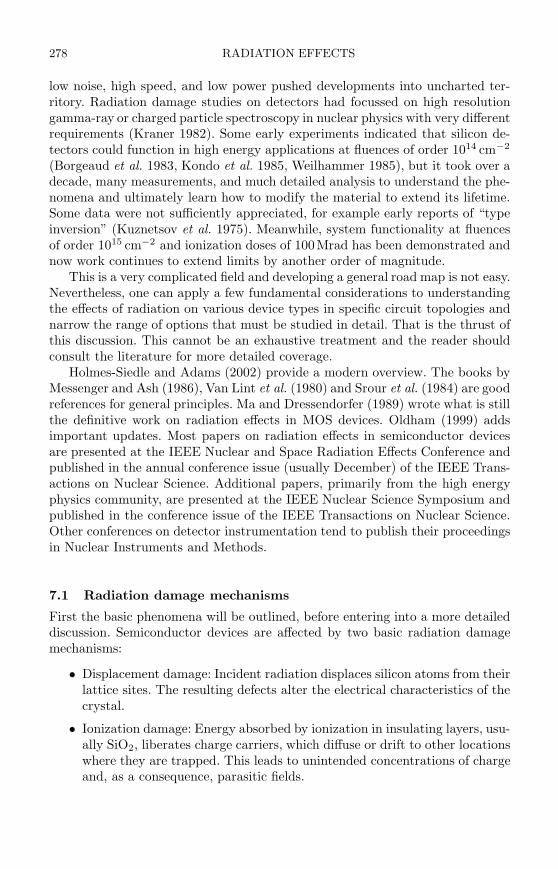
278 RADIATION EFFECTS
low noise, high speed, and low power pushed developments into uncharted ter-ritory. Radiation damage studies on detectors had focussed on high resolutiongamma-ray or charged particle spectroscopy in nuclear physics with very differentrequirements (Kraner 1982). Some early experiments indicated that silicon de-tectors could function in high energy applications at fluences of order 1014 cm−2
(Borgeaud et al. 1983, Kondo et al. 1985, Weilhammer 1985), but it took over adecade, many measurements, and much detailed analysis to understand the phe-nomena and ultimately learn how to modify the material to extend its lifetime.Some data were not sufficiently appreciated, for example early reports of “typeinversion” (Kuznetsov et al. 1975). Meanwhile, system functionality at fluencesof order 1015 cm−2 and ionization doses of 100Mrad has been demonstrated andnow work continues to extend limits by another order of magnitude.
This is a very complicated field and developing a general road map is not easy.Nevertheless, one can apply a few fundamental considerations to understandingthe effects of radiation on various device types in specific circuit topologies andnarrow the range of options that must be studied in detail. That is the thrust ofthis discussion. This cannot be an exhaustive treatment and the reader shouldconsult the literature for more detailed coverage.
Holmes-Siedle and Adams (2002) provide a modern overview. The books byMessenger and Ash (1986), Van Lint et al. (1980) and Srour et al. (1984) are goodreferences for general principles. Ma and Dressendorfer (1989) wrote what is stillthe definitive work on radiation effects in MOS devices. Oldham (1999) addsimportant updates. Most papers on radiation effects in semiconductor devicesare presented at the IEEE Nuclear and Space Radiation Effects Conference andpublished in the annual conference issue (usually December) of the IEEE Trans-actions on Nuclear Science. Additional papers, primarily from the high energyphysics community, are presented at the IEEE Nuclear Science Symposium andpublished in the conference issue of the IEEE Transactions on Nuclear Science.Other conferences on detector instrumentation tend to publish their proceedingsin Nuclear Instruments and Methods.
7.1 Radiation damage mechanisms
First the basic phenomena will be outlined, before entering into a more detaileddiscussion. Semiconductor devices are affected by two basic radiation damagemechanisms:
• Displacement damage: Incident radiation displaces silicon atoms from theirlattice sites. The resulting defects alter the electrical characteristics of thecrystal.
• Ionization damage: Energy absorbed by ionization in insulating layers, usu-ally SiO2, liberates charge carriers, which diffuse or drift to other locationswhere they are trapped. This leads to unintended concentrations of chargeand, as a consequence, parasitic fields.
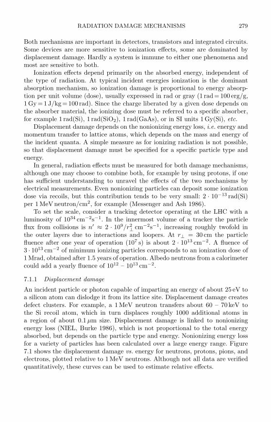
RADIATION DAMAGE MECHANISMS 279
Both mechanisms are important in detectors, transistors and integrated circuits.Some devices are more sensitive to ionization effects, some are dominated bydisplacement damage. Hardly a system is immune to either one phenomena andmost are sensitive to both.
Ionization effects depend primarily on the absorbed energy, independent ofthe type of radiation. At typical incident energies ionization is the dominantabsorption mechanism, so ionization damage is proportional to energy absorp-tion per unit volume (dose), usually expressed in rad or gray (1 rad=100 erg/g,1 Gy =1J/kg=100 rad). Since the charge liberated by a given dose depends onthe absorber material, the ionizing dose must be referred to a specific absorber,for example 1 rad(Si), 1 rad(SiO2), 1 rad(GaAs), or in SI units 1 Gy(Si), etc.
Displacement damage depends on the nonionizing energy loss, i.e. energy andmomentum transfer to lattice atoms, which depends on the mass and energy ofthe incident quanta. A simple measure as for ionizing radiation is not possible,so that displacement damage must be specified for a specific particle type andenergy.
In general, radiation effects must be measured for both damage mechanisms,although one may choose to combine both, for example by using protons, if onehas sufficient understanding to unravel the effects of the two mechanisms byelectrical measurements. Even nonionizing particles can deposit some ionizationdose via recoils, but this contribution tends to be very small: 2 · 10−13 rad(Si)per 1 MeV neutron/cm2, for example (Messenger and Ash 1986).
To set the scale, consider a tracking detector operating at the LHC with aluminosity of 1034 cm−2s−1. In the innermost volume of a tracker the particleflux from collisions is n′ ≈ 2 · 109/r2
⊥ cm−2s−1, increasing roughly twofold inthe outer layers due to interactions and loopers. At r⊥ = 30 cm the particlefluence after one year of operation (107 s) is about 2 · 1013 cm−2. A fluence of3 · 1013 cm−2 of minimum ionizing particles corresponds to an ionization dose of1 Mrad, obtained after 1.5 years of operation. Albedo neutrons from a calorimetercould add a yearly fluence of 1012 – 1013 cm−2.
7.1.1 Displacement damage
An incident particle or photon capable of imparting an energy of about 25 eV toa silicon atom can dislodge it from its lattice site. Displacement damage createsdefect clusters. For example, a 1 MeV neutron transfers about 60 – 70 keV tothe Si recoil atom, which in turn displaces roughly 1000 additional atoms ina region of about 0.1 µm size. Displacement damage is linked to nonionizingenergy loss (NIEL, Burke 1986), which is not proportional to the total energyabsorbed, but depends on the particle type and energy. Nonionizing energy lossfor a variety of particles has been calculated over a large energy range. Figure7.1 shows the displacement damage vs. energy for neutrons, protons, pions, andelectrons, plotted relative to 1 MeV neutrons. Although not all data are verifiedquantitatively, these curves can be used to estimate relative effects.
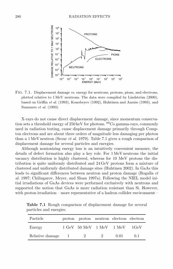
280 RADIATION EFFECTS
10-4
10-3
10-2
10-1
100
101
102
103
104
ENERGY (MeV)
10-5
10-4
10-3
10-2
10-1
100
101
102
103
104
DAMAGERELATIVETO
1MeVNEUTRONS
PROTONS
NEUTRONS
PIONS
ELECTRONS
Fig. 7.1. Displacement damage vs. energy for neutrons, protons, pions, and electrons,
plotted relative to 1 MeV neutrons. The data were compiled by Lindstrom (2000),
based on Griffin et al. (1993), Konobeyev (1992), Huhtinen and Aarnio (1993), and
Summers et al. (1993).
X-rays do not cause direct displacement damage, since momentum conserva-tion sets a threshold energy of 250keV for photons. 60Co gamma-rays, commonlyused in radiation testing, cause displacement damage primarily through Comp-ton electrons and are about three orders of magnitude less damaging per photonthan a 1MeV neutron (Srour et al. 1979). Table 7.1 gives a rough comparison ofdisplacement damage for several particles and energies.
Although nonionizing energy loss is an intuitively convenient measure, thedetails of defect formation also play a key role. For 1MeV neutrons the initialvacancy distribution is highly clustered, whereas for 10 MeV protons the dis-tribution is quite uniformly distributed and 24GeV protons form a mixture ofclustered and uniformly distributed damage sites (Huhtinen 2002). In GaAs thisleads to significant differences between neutron and proton damage (Rogalla etal. 1997; Chilingarov, Meyer, and Sloan 1997a). Following the NIEL model ini-tial irradiations of GaAs devices were performed exclusively with neutrons andsupported the notion that GaAs is more radiation resistant than Si. However,with proton irradiation – more representative of a hadron collider environment –
Table 7.1 Rough comparison of displacement damage for severalparticles and energies.
Particle proton proton neutron electron electron
Energy 1 GeV 50 MeV 1 MeV 1 MeV 1GeV
Relative damage 1 2 2 0.01 0.1
RADIATION DAMAGE MECHANISMS 281
HOLEEMISSION
ELECTRONEMISSION
ELECTRONCAPTURE
HOLECAPTURE
TRAPPING
(a) (b) (c) (d) (e)
Fig. 7.2. Emission and capture processes through intermediate states. The arrows
show the direction of electron transitions.
the contrary proved to be true. In a microscopic analysis Huhtinen (2002) arguesthat there is no obvious reason why NIEL scaling should be valid, so the prudentapproach is to measure the effects of radiation with particles and energies rep-resentative of the actual radiation environment. Messenger et al. (2004) discusslimits to the application of the NIEL concept.
Displacement damage manifests itself in three important ways:
• Formation of mid-gap states, which facilitate the transition of electronsfrom the valence to the conduction band. In depletion regions this leadsto a generation current, i.e. an increase in the current of reverse-biasedpn-junctions. In forward biased junctions or nondepleted regions mid-gapstates facilitate recombination, i.e. charge loss.
• States close to the band edges facilitate trapping, where charge is capturedand released after some time.
• A change in doping characteristics (effective donor or acceptor density).
The role of mid-gap states is illustrated in Figure 7.2 (for a quantitative treat-ment see Appendix F). Because interband transitions in Si require momentumtransfer (“indirect bandgap”), direct transitions between the conduction andvalence bands are extremely improbable (unlike GaAs, for example). The intro-duction of intermediate states in the forbidden gap provides “stepping stones” foremission and capture processes. The individual steps, emission of holes or elec-trons and capture of electrons or holes, are illustrated in Figure 7.2. As shownin Figure 7.2 (a) the process of hole emission from a defect can also be viewedas promoting an electron from the valence band to the defect level. In a sec-ond step (b) this electron can proceed to the conduction band and contributeto current flow – generation current. Conversely, a defect state can capture anelectron from the conduction band (c), which in turn can capture a hole (d).This “recombination” process reduces current flowing in the conduction band.
Since the transition probabilities are exponential functions of the energy dif-ferences, all processes that involve transitions between both bands require mid-gap states to proceed at an appreciable rate. Given a distribution of states these
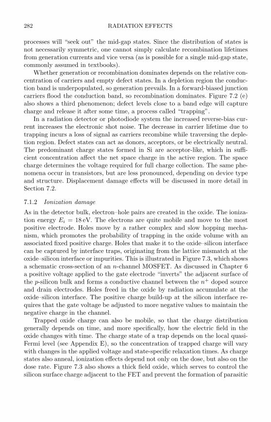
282 RADIATION EFFECTS
processes will “seek out” the mid-gap states. Since the distribution of states isnot necessarily symmetric, one cannot simply calculate recombination lifetimesfrom generation currents and vice versa (as is possible for a single mid-gap state,commonly assumed in textbooks).
Whether generation or recombination dominates depends on the relative con-centration of carriers and empty defect states. In a depletion region the conduc-tion band is underpopulated, so generation prevails. In a forward-biased junctioncarriers flood the conduction band, so recombination dominates. Figure 7.2 (e)also shows a third phenomenon; defect levels close to a band edge will capturecharge and release it after some time, a process called “trapping”.
In a radiation detector or photodiode system the increased reverse-bias cur-rent increases the electronic shot noise. The decrease in carrier lifetime due totrapping incurs a loss of signal as carriers recombine while traversing the deple-tion region. Defect states can act as donors, acceptors, or be electrically neutral.The predominant charge states formed in Si are acceptor-like, which in suffi-cient concentration affect the net space charge in the active region. The spacecharge determines the voltage required for full charge collection. The same phe-nomena occur in transistors, but are less pronounced, depending on device typeand structure. Displacement damage effects will be discussed in more detail inSection 7.2.
7.1.2 Ionization damage
As in the detector bulk, electron–hole pairs are created in the oxide. The ioniza-tion energy Ei = 18 eV. The electrons are quite mobile and move to the mostpositive electrode. Holes move by a rather complex and slow hopping mecha-nism, which promotes the probability of trapping in the oxide volume with anassociated fixed positive charge. Holes that make it to the oxide–silicon interfacecan be captured by interface traps, originating from the lattice mismatch at theoxide–silicon interface or impurities. This is illustrated in Figure 7.3, which showsa schematic cross-section of an n-channel MOSFET. As discussed in Chapter 6a positive voltage applied to the gate electrode “inverts” the adjacent surface ofthe p-silicon bulk and forms a conductive channel between the n+ doped sourceand drain electrodes. Holes freed in the oxide by radiation accumulate at theoxide–silicon interface. The positive charge build-up at the silicon interface re-quires that the gate voltage be adjusted to more negative values to maintain thenegative charge in the channel.
Trapped oxide charge can also be mobile, so that the charge distributiongenerally depends on time, and more specifically, how the electric field in theoxide changes with time. The charge state of a trap depends on the local quasi-Fermi level (see Appendix E), so the concentration of trapped charge will varywith changes in the applied voltage and state-specific relaxation times. As chargestates also anneal, ionization effects depend not only on the dose, but also on thedose rate. Figure 7.3 also shows a thick field oxide, which serves to control thesilicon surface charge adjacent to the FET and prevent the formation of parasitic
RADIATION DAMAGE IN DIODES 283
GATE OXIDE FIELD OXIDE
S G D
0 V
V
VV+ +++
CHANNEL
p BULK
DETAIL OFGATE OXIDE
SILICON
SiO2
n n+ +
Fig. 7.3. Schematic cross-section of an n-channel MOSFET (left). A detail of the
gate oxide shows the trapped holes at the oxide–silicon interface (right).
channels to adjacent devices. The same positive charge build-up as in the gateoxide also occurs here, indeed it can be exacerbated because the field oxide isquite thick. We’ll return to these phenomena in Sections 7.3.1 and 7.3.3. For adetailed discussion, see the texts by Ma and Dressendorfer (1989) and Oldham(1999).
In summary, ionization effects are determined by
• interface trapped charge,
• oxide trapped charge,
• the mobility of trapped charge, and
• the time and voltage dependence of charge states.
Although the primary radiation damage depends only on the absorbed ionizingenergy, the resulting effects of this dose depend on the rate of irradiation, theapplied voltages and their time variation, the temperature, and the time variationof the radiation itself. Ionization damage manifests itself most clearly in MOSfield effect transistors, so it will be discussed in more detail in that section.
7.2 Radiation damage in diodes
Diode structures are basic components of more complex devices, for examplebipolar transistors, junction FETs and integrated circuits. Since the characteris-tics of diode depletion regions depend primarily on bulk properties, displacementdamage is the key damage mechanism. Reverse-biased diodes with large deple-tion depths are used as radiation detectors and photodiodes. Because of theirlarge depletion depths, typically hundreds of microns, detector diodes are verysensitive to bulk damage and extensive work by the high-energy physics com-munity has produced many insights into bulk radiation effects. Affected are thedetector leakage current, the doping characteristics, and charge collection.
284 RADIATION EFFECTS
A theoretical analysis from first principles is quite complex, due to the manyphenomena involved. Take doping changes as an example. A key mechanism isthat defects are mobile. Silicon interstitials are quite active and displace eitherP donors or B acceptors from substitutional sites and render them electricallyinactive. These interstitial dopants together with oxygen, commonly present inthe lattice as an impurity, react in very different ways with vacancies to formcomplexes with a variety of electronic characteristics (see Tsveybak et al. 1992,Huhtinen 2002 and references therein). Fortuitously, although a multitude ofcompeting effects can be invoked to predict and interpret experimental results,the data can be described by rather simple parameterizations.
7.2.0.1 Reverse bias current The increase in reverse bias current (leakage cur-rent) is linked to the creation of mid-gap states, as discussed in Appendix F.Experimental data are consistent with a uniform distribution of active defectsin the detector volume. The diode bias current after irradiation
Id = I0 + α · Φ · Ad , (7.1)
where I0 is the bias current before irradiation, α is a damage coefficient depen-dent on particle type and fluence, Φ is the particle fluence, and the productof detector area and thickness Ad is the detector volume. For 650MeV pro-tons α ≈ 3 · 10−17 A/cm (Barberis et al. 1993, Chilingarov et al. 1995) andfor 1 MeV neutrons (characteristic of the albedo emanating from a calorimeter)α = 4 · 10−17 A/cm (Moll 1999). The parameterization used in eqn. 7.1 is quitegeneral, as it merely assumes a spatially uniform formation of electrically activedefects in the detector volume, without depending on the details of energy levelsor states. Unlike a high-quality diode, where reverse current saturates well belowthe depletion voltage, in a radiation-damaged diode the reverse bias current in-creases roughly with the square root of voltage, due to the uniform distributionof radiation damage sites.
After initial defect formation the leakage current decreases with time. Severalprocesses appear to contribute to the annealing process, as a sum of exponen-tials with various time constants gives a good fit to the data (Wunstorf 1992,Chilingarov et al. 1995). The ROSE collaboration (Lindstrom 2001) adopted aprescription in which the leakage current is measured after 80min. annealing at60 C. This procedure yields the same damage coefficient for a wide range of ir-radiations. The results apply to both n- and p-type material, whether float zone,Czochralski, or epitaxially grown, and over a wide range of resistivities.
The coefficients given above apply to operation at 20 C. The reverse biascurrent is strongly dependent on temperature. Even after rather low fluences thegeneration current dominates (see Appendix F), so the reverse bias current
IR(T ) ∝ T 2e−E/2kT . (7.2)
For radiation damaged samples an activation energy E = 1.2 eV has provideda good fit (Barberis et al. 1993, Gill et al. 1992, Ohsugi et al. 1988), whereas
RADIATION DAMAGE IN DIODES 285
unirradiated samples usually exhibit E = 1.12 eV, the gap energy. The ratio ofcurrents at two temperatures T1 and T2 is
IR(T2)
IR(T1)=
(
T2
T1
)2
exp
[
− E
2k
(
T1 − T2
T1T2
)]
. (7.3)
In practice, the variation of leakage current with temperature is very reproduciblefrom device to device, even after substantial doping changes due to radiationdamage. The leakage current can be used for dosimetry and diodes are offeredcommercially specifically for this purpose.
7.2.0.2 Doping characteristics The effect of displacement damage on dopingcharacteristics has been investigated extensively in the course of detector studiesfor the LHC and is still the subject of ongoing study. Measurements on a varietyof strip detectors and photodiodes by groups in the U.S., Japan and Europe haveshown that the effective doping of n-type silicon initially decreases, appears in-trinsic (i.e. undoped), and then turns p-like (“type inversion”), with the effectivedoping (or more accurately, space charge) increasing with fluence.
One contribution is donor removal (Pitzl et al. 1992, Giubellino et al. 1992),but this by itself would only reduce the n-type nature of the material. “Typeinversion” is consistent with the notion that acceptor sites are formed by theirradiation. Before irradiation the depletion region shows a space charge fromthe dopant host atoms, so in n-type material the space charge is positive. Theapplied bias voltage is required not only to deplete the detector, but also tocollective mobile charge against the field set up by the space charge. Displacementdamage forms acceptor-like states, which are populated by electrons from thebulk through thermal excitation, so they form a negative space charge. Initially,the positive space charge decreases as new acceptor states neutralize originaldonor states. At some fluence the two balance, so the space charge is zero, andbeyond this fluence the acceptor states dominate yielding a net negative spacecharge. Note that “type inversion” is not associated with the creation of mobileholes, so although the material appears p-like, it is not the same as conventionalp-doped material (Li 1994). As the change in space charge results from multiplesequential processes, its evolution is temperature dependent, as will be describedbelow.
Operationally, the change in space charge appears as a change in doping level,so the net space charge is commonly referred to as an effective doping level Neff .The detector functions as before and no change in bias polarity is needed, but totransport charge through the full detector thickness d the voltage must be raisedproportionally to the increase in space charge
V =e
2ε|Neff | d2 . (7.4)
In analogy to conventional diode operation this is often referred to as the “de-pletion voltage”, although the device is devoid of mobile charge even at smaller
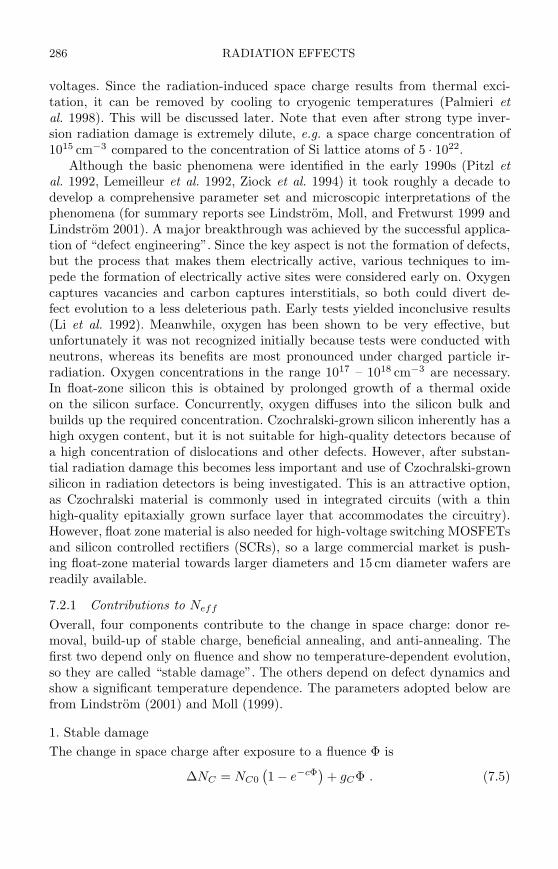
286 RADIATION EFFECTS
voltages. Since the radiation-induced space charge results from thermal exci-tation, it can be removed by cooling to cryogenic temperatures (Palmieri etal. 1998). This will be discussed later. Note that even after strong type inver-sion radiation damage is extremely dilute, e.g. a space charge concentration of1015 cm−3 compared to the concentration of Si lattice atoms of 5 · 1022.
Although the basic phenomena were identified in the early 1990s (Pitzl etal. 1992, Lemeilleur et al. 1992, Ziock et al. 1994) it took roughly a decade todevelop a comprehensive parameter set and microscopic interpretations of thephenomena (for summary reports see Lindstrom, Moll, and Fretwurst 1999 andLindstrom 2001). A major breakthrough was achieved by the successful applica-tion of “defect engineering”. Since the key aspect is not the formation of defects,but the process that makes them electrically active, various techniques to im-pede the formation of electrically active sites were considered early on. Oxygencaptures vacancies and carbon captures interstitials, so both could divert de-fect evolution to a less deleterious path. Early tests yielded inconclusive results(Li et al. 1992). Meanwhile, oxygen has been shown to be very effective, butunfortunately it was not recognized initially because tests were conducted withneutrons, whereas its benefits are most pronounced under charged particle ir-radiation. Oxygen concentrations in the range 1017 – 1018 cm−3 are necessary.In float-zone silicon this is obtained by prolonged growth of a thermal oxideon the silicon surface. Concurrently, oxygen diffuses into the silicon bulk andbuilds up the required concentration. Czochralski-grown silicon inherently has ahigh oxygen content, but it is not suitable for high-quality detectors because ofa high concentration of dislocations and other defects. However, after substan-tial radiation damage this becomes less important and use of Czochralski-grownsilicon in radiation detectors is being investigated. This is an attractive option,as Czochralski material is commonly used in integrated circuits (with a thinhigh-quality epitaxially grown surface layer that accommodates the circuitry).However, float zone material is also needed for high-voltage switching MOSFETsand silicon controlled rectifiers (SCRs), so a large commercial market is push-ing float-zone material towards larger diameters and 15 cm diameter wafers arereadily available.
7.2.1 Contributions to Neff
Overall, four components contribute to the change in space charge: donor re-moval, build-up of stable charge, beneficial annealing, and anti-annealing. Thefirst two depend only on fluence and show no temperature-dependent evolution,so they are called “stable damage”. The others depend on defect dynamics andshow a significant temperature dependence. The parameters adopted below arefrom Lindstrom (2001) and Moll (1999).
1. Stable damage
The change in space charge after exposure to a fluence Φ is
∆NC = NC0
(
1 − e−cΦ)
+ gCΦ . (7.5)
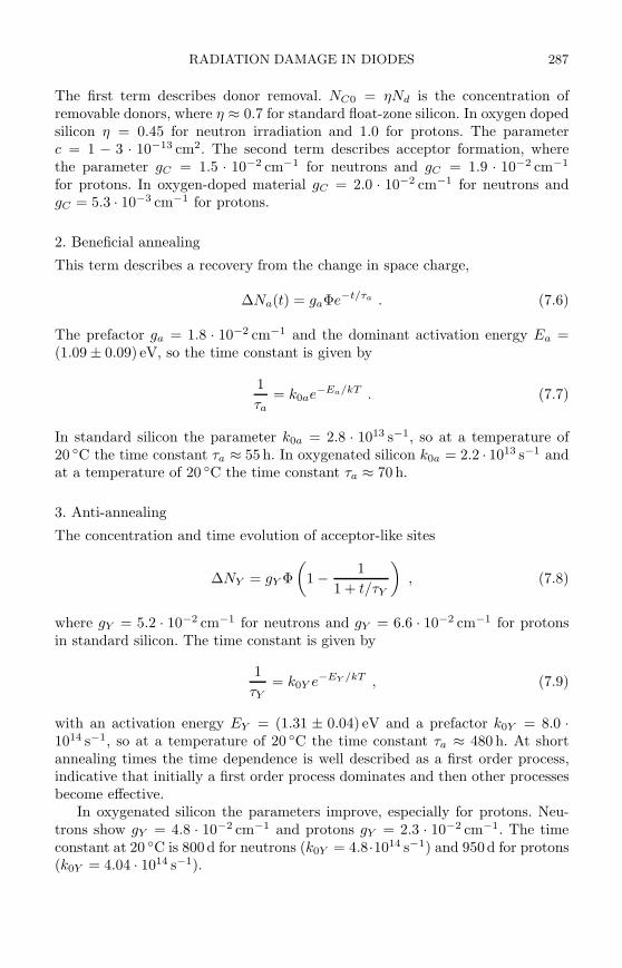
RADIATION DAMAGE IN DIODES 287
The first term describes donor removal. NC0 = ηNd is the concentration ofremovable donors, where η ≈ 0.7 for standard float-zone silicon. In oxygen dopedsilicon η = 0.45 for neutron irradiation and 1.0 for protons. The parameterc = 1 − 3 · 10−13 cm2. The second term describes acceptor formation, wherethe parameter gC = 1.5 · 10−2 cm−1 for neutrons and gC = 1.9 · 10−2 cm−1
for protons. In oxygen-doped material gC = 2.0 · 10−2 cm−1 for neutrons andgC = 5.3 · 10−3 cm−1 for protons.
2. Beneficial annealing
This term describes a recovery from the change in space charge,
∆Na(t) = gaΦe−t/τa . (7.6)
The prefactor ga = 1.8 · 10−2 cm−1 and the dominant activation energy Ea =(1.09 ± 0.09) eV, so the time constant is given by
1
τa= k0ae−Ea/kT . (7.7)
In standard silicon the parameter k0a = 2.8 · 1013 s−1, so at a temperature of20 C the time constant τa ≈ 55 h. In oxygenated silicon k0a = 2.2 · 1013 s−1 andat a temperature of 20 C the time constant τa ≈ 70 h.
3. Anti-annealing
The concentration and time evolution of acceptor-like sites
∆NY = gY Φ
(
1 − 1
1 + t/τY
)
, (7.8)
where gY = 5.2 · 10−2 cm−1 for neutrons and gY = 6.6 · 10−2 cm−1 for protonsin standard silicon. The time constant is given by
1
τY= k0Y e−EY /kT , (7.9)
with an activation energy EY = (1.31 ± 0.04) eV and a prefactor k0Y = 8.0 ·1014 s−1, so at a temperature of 20 C the time constant τa ≈ 480 h. At shortannealing times the time dependence is well described as a first order process,indicative that initially a first order process dominates and then other processesbecome effective.
In oxygenated silicon the parameters improve, especially for protons. Neu-trons show gY = 4.8 · 10−2 cm−1 and protons gY = 2.3 · 10−2 cm−1. The timeconstant at 20 C is 800d for neutrons (k0Y = 4.8·1014 s−1) and 950d for protons(k0Y = 4.04 · 1014 s−1).
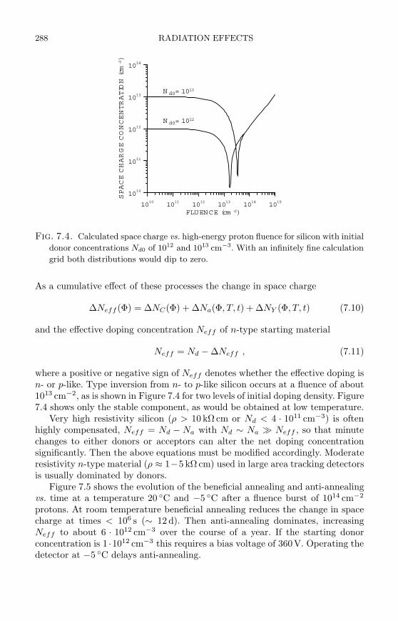
288 RADIATION EFFECTS
1010 1011 1012 1013 1014 1015
FLUENCE (cm -2)
1010
1011
1012
1013
1014
SPACECHARGECONCENTRATION(cm
-3)
N d0= 1013
N d0= 1012
Fig. 7.4. Calculated space charge vs. high-energy proton fluence for silicon with initial
donor concentrations Nd0 of 1012 and 1013 cm−3. With an infinitely fine calculation
grid both distributions would dip to zero.
As a cumulative effect of these processes the change in space charge
∆Neff (Φ) = ∆NC(Φ) + ∆Na(Φ, T, t) + ∆NY (Φ, T, t) (7.10)
and the effective doping concentration Neff of n-type starting material
Neff = Nd − ∆Neff , (7.11)
where a positive or negative sign of Neff denotes whether the effective doping isn- or p-like. Type inversion from n- to p-like silicon occurs at a fluence of about1013 cm−2, as is shown in Figure 7.4 for two levels of initial doping density. Figure7.4 shows only the stable component, as would be obtained at low temperature.
Very high resistivity silicon (ρ > 10 kΩ cm or Nd < 4 · 1011 cm−3) is oftenhighly compensated, Neff = Nd − Na with Nd ∼ Na ≫ Neff , so that minutechanges to either donors or acceptors can alter the net doping concentrationsignificantly. Then the above equations must be modified accordingly. Moderateresistivity n-type material (ρ ≈ 1−5 kΩ cm) used in large area tracking detectorsis usually dominated by donors.
Figure 7.5 shows the evolution of the beneficial annealing and anti-annealingvs. time at a temperature 20 C and −5 C after a fluence burst of 1014 cm−2
protons. At room temperature beneficial annealing reduces the change in spacecharge at times < 106 s (∼ 12 d). Then anti-annealing dominates, increasingNeff to about 6 · 1012 cm−3 over the course of a year. If the starting donorconcentration is 1 ·1012 cm−3 this requires a bias voltage of 360V. Operating thedetector at −5 C delays anti-annealing.
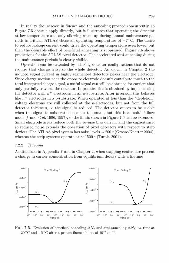
RADIATION DAMAGE IN DIODES 289
In reality the increase in fluence and the annealing proceed concurrently, soFigure 7.5 doesn’t apply directly, but it illustrates that operating the detectorat low temperature and only allowing warm-up during annual maintenance pe-riods is critical. ATLAS chose an operating temperature of −7 C. The desireto reduce leakage current could drive the operating temperature even lower, butthen the desirable effect of beneficial annealing is suppressed. Figure 7.6 showspredictions for the ATLAS pixel detector. The accelerated anti-annealing duringthe maintenance periods is clearly visible.
Operation can be extended by utilizing detector configurations that do notrequire that charge traverse the whole detector. As shown in Chapter 2 theinduced signal current in highly segmented detectors peaks near the electrode.Since charge motion near the opposite electrode doesn’t contribute much to thetotal integrated charge signal, a useful signal can still be obtained for carriers thatonly partially traverse the detector. In practice this is obtained by implementingthe detector with n+ electrodes in an n-substrate. After inversion this behaveslike n+ electrodes in a p-substrate. When operated at less than the “depletion”voltage electrons are still collected at the n-electrodes, but not from the fulldetector thickness, so the signal is reduced. The detector ceases to be usablewhen the signal-to-noise ratio becomes too small, but this is a “soft” failuremode (Unno et al. 1996, 1997), so the limits shown in Figure 7.6 can be extended.Small electrode areas reduce both the reverse bias current and the capacitance,so reduced noise extends the operation of pixel detectors with respect to stripdevices. The ATLAS pixel system has noise levels ∼ 200 e (Grosse-Knetter 2004),whereas the strip systems operate at ∼ 1500 e (Turala 2001).
7.2.2 Trapping
As discussed in Appendix F and in Chapter 2, when trapping centers are presenta change in carrier concentration from equilibrium decays with a lifetime
102
103
104
105
106
107
108
109
1010
TIM E (s)
2x10¹²
4x10¹²
6x10¹²
8x10¹²
1x10¹³
Neff(cm-3)
T = 20 deg C
N a
N Y
102
103
104
105
106
107
108
109
1010
TIM E (s)
2x10¹²
3x10¹²
4x10¹²
5x10¹²
6x10¹²
Neff(cm-3)
N C
T = -5 deg C
N aN Y
N C
Fig. 7.5. Evolution of beneficial annealing ∆Na and anti-annealing ∆NY vs. time at
20 C and −5 C after a proton fluence burst of 1014 cm−2.
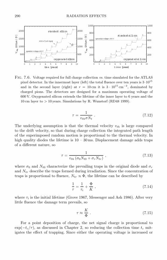
290 RADIATION EFFECTS
0 1 2 3 4 5 6 7 8 9 10
time [years]
500
1000
1500
2000
Vdep(200µm)[V]
500
1000
1500
2000standard silicon
oxygenated silicon
operation voltage: 600 V
6000 e for B-layer6000 e for B-layer
0 1 2 3 4 5 6 7 8 9 10
time [years]
200
400
600
800
1000
Vdep(250µm)[V]
200
400
600
800
1000
standard silicon
oxygenated silicon
operation voltage: 600 V
Fig. 7.6. Voltage required for full charge collection vs. time simulated for the ATLAS
pixel detector. In the innermost layer (left) the total fluence over ten years is 3 ·1015
and in the second layer (right) at r = 10 cm it is 3 · 1015 cm−2, dominated by
charged pions. The detectors are designed for a maximum operating voltage of
600 V. Oxygenated silicon extends the lifetime of the inner layer to 6 years and the
10 cm layer to > 10 years. Simulations by R. Wunstorf (RD48 1999).
τ =1
vthσNt. (7.12)
The underlying assumption is that the thermal velocity vth is large comparedto the drift velocity, so that during charge collection the integrated path lengthof the superimposed random motion is proportional to the thermal velocity. Inhigh quality diodes the lifetime is 10 – 30ms. Displacement damage adds trapsof a different nature, so
τ =1
vth (σ0Nt0 + σrNtr), (7.13)
where σ0 and Nt0 characterize the prevailing traps in the original diode and σr
and Ntr describe the traps formed during irradiation. Since the concentration oftraps is proportional to fluence, Ntr ∝ Φ, the lifetime can be described by
1
τ=
1
τi+
Φ
K, (7.14)
where τi is the initial lifetime (Grove 1967, Messenger and Ash 1986). After verylittle fluence the damage term prevails, so
τ ≈ K
Φ. (7.15)
For a point deposition of charge, the net signal charge is proportional toexp(−tc/τ), as discussed in Chapter 2, so reducing the collection time tc mit-igates the effect of trapping. Since either the operating voltage is increased or
RADIATION DAMAGE IN DIODES 291
depletion widths are reduced at damage levels where charge trapping is appre-ciable, fields tend to be higher and collection times decrease automatically withradiation damage, provided the detector can sustain the higher fields. The mo-bilities of electrons and holes appear to be unaffected by heavy radiation damage(Brodbeck et al. 2002).
Kramberger et al. (2002) irradiated a diverse set of samples with initial resis-tivities ranging from 1 to 15 kΩ cm using both standard and oxygenated siliconwith neutrons, pions, and protons to fluences up to 2 · 1014 cm2 and obtain for
neutrons : Ke = (2.44± 0.06) · 106 s/cm2 Kh = (1.67 ± 0.06) · 106 s/cm2,
pions : Ke = (1.75± 0.06) · 106 s/cm2
Kh = (1.30 ± 0.03) · 106 s/cm2,
protons : Ke = (1.79± 0.06) · 106 s/cm2
Kh = (1.30 ± 0.03) · 106 s/cm2.
The errors are statistical and don’t include a 10% uncertainty in the measuredfluence. Krasel et al. (2004) irradiated oxygenated detectors with 24 GeV/c pro-tons to neutron-equivalent fluences ranging from 2 · 1013 to 9 · 1014 cm−2 andfound
Ke = (1.95± 0.06) · 106 s/cm2
Kh = (1.98± 0.07) · 106 s/cm2
for electrons and holes, respectively. In test beam measurements of four prototypeATLAS pixel modules exposed to a neutron-equivalent fluence of 1.1 · 1015 cm−2
Troncon et al. find an average lifetime of (4.1 ± 0.3 ± 0.6) ns (Troncon 2004).Note that although the trapping constants Ke and Kh are similar, since holes
move about three times slower than electrons, their effective drift length is threetimes smaller than for electrons. Thus, detector structures that emphasize theelectron signal provide a higher charge collection efficiency.
Assuming K ≈ 2 · 106, the carrier lifetime at a fluence of 1014 is 20 ns. Ina 300 µm thick detector operated at 300V the average field is 104 V/cm, sothe drift velocity v = 7 · 106 cm/s. The collection time is 4 ns, so little chargeis lost to trapping. At a fluence of 1015, however, the lifetime drops to about2 ns. Operating a 250 µm thick detector at 600 V yields an average field of 2.4 ·104 V/cm. Because of nonconstant mobility the drift velocity only increases tov = 9 ·106 cm/s, practically saturation velocity, so the estimated drift time is 3 nsand a substantial charge loss is expected. These are only estimates to illustratethe problem. Although the potential distribution appears to be as expected fora partially depleted detector with the maximum field at the n-contact droppinglinearly into the bulk, an additional high field region appears near the p-contact(Beattie et al. 1998, Wunstorf 1992, Krasel et al. 2004, Castaldini et al. 2002,Eremin, Verbitskaya, and Li 2002). More detailed simulations indicate 50 – 60%charge collection efficiency for tracks traversing the detector after a fluence of1015 cm−2, falling off to about 25% after a fluence of 5 · 1015 (Krasel et al.2004). Test beam measurements of complete ATLAS pixel modules using n-side
292 RADIATION EFFECTS
readout of “n-on-n” pixels (see Section 7.5) in oxygenated silicon achieved nearlyfull charge collection efficiency in 250 µm thick sensors operated at 700V afterexposure to a neutron-equivalent fluence of 1.1 · 1015 cm−2 (Troncon 2004).
7.2.3 Ionization effects
The basic detector is insensitive to ionization effects. In the bulk, ionizing radia-tion creates electrons and holes that are swept from the sensitive volume; chargecan flow freely through the external circuitry to restore equilibrium. A potentialproblem lies in the peripheral structures, the oxide layers that are essential tocontrolling leakage paths at the edge of the diode and to preserving interelectrodeisolation in segmented detectors.
The positive space charge due to hole trapping in the oxide and at the in-terface (see Figure 7.3) attracts electrons in the silicon bulk to the interface.These accumulation layers can exhibit high local electron densities and formconducting channels, for example between the detector electrodes. This is es-pecially critical at the “ohmic” electrodes in double-sided detectors, where theabsence of pn-junctions makes operation reliant on full depletion of the siliconsurface (see Appendix A). Even without radiation, the silicon surface tends tobe n-type, so the ohmic side of n-type detectors is inherently more difficult tocontrol (Barberis et al. 1994, Wheadon et al. 1994). Before irradiation the inter-strip resistance tends to be very high, so small increases in surface charge havea big effect. However, to prevent signal leakage from one strip to another, therequirement is only that the interstrip impedance remain large with respect tothe input impedance of the amplifier, which in strip detector systems is typically100 – 1000ohms.
Some detectors include integrated coupling capacitors and biasing networks.Biasing structures such as punch-through resistors and MOSFET structuresare subject to ionization damage (Azzi et al. 1996). Although these devicescan remain functional, substantial changes in voltage drop have been reportedfor punch-through and accumulation layer devices, whereas measurements onpolysilicon resistors irradiated to 4Mrad (65MeV protons) show no effect (Kub-ota et al. 1991).
7.3 Radiation damage in transistors and integrated circuits
In principle, the same phenomena discussed for detectors also occur in transis-tors, except that the geometries of transistors are much smaller (depletion widths< 1 µm) and the typical doping levels are higher (> 1015 cm−3).
7.3.1 Bipolar transistors
The most important damage mechanism in bipolar transistors is the degrada-tion of DC gain at low currents. The damage mechanism is the same that causesincreased leakage current in detectors, formation of mid-gap states by displace-ment damage. The difference is that the base–emitter junction is forward biased,so the high carrier concentration in the conduction band tips the balance from
RADIATION DAMAGE IN TRANSISTORS AND INTEGRATED CIRCUITS 293
generation to recombination (see Figure 7.2 and Appendix F). The fractionalcarrier loss depends on the relative concentrations of injected carriers and de-fects. Consequently, the reduction of DC gain due to radiation damage dependson current density. For a given collector current a small device (small emitterarea) will suffer less degradation in DC gain than a large one.
Since the probability of recombination depends on the transit time throughthe junction region, reduced base width will also improve the radiation resistance.Base width is strongly linked with device speed, so that the reduction in DC gainβDC from its pre-irradiation value β0 scales inversely with a transistor’s unitygain frequency fT (Messenger and Ash 1986 and see Appendix G),
1
β− 1
β0= KΦ ∝ Φ
fT. (7.16)
Since IC technology is driven primarily by device speed, mainstream marketforces indirectly improve the radiation resistance of bipolar transistor processes.Mid-gap states also limit the low current performance before irradiation. Overthe past decade, evolutionary improvements in contamination control and pro-cess technology have also yielded substantially better low-current performance.Measurements on bipolar transistors from several vendors have shown that pro-cesses not specifically designed for radiation resistance are indeed quite usablein severe radiation environments, even at low currents. (Cartiglia et al. 1992,Kipnis, Spieler, and Collins 1994, Spencer et al. 1995).
Changes in doping levels due to radiation have little effect in bipolar tran-sistors. Typical doping levels in the base and emitter are NB = 1018 and NE =1020 cm−3. In the collector depletion region doping levels are smaller, typically1016, rising to 1018 or 1019 at the collector contact. At these levels the change indoping level due to displacement damage (∆NA ≈ 1012 cm−3 at Φ = 1014 cm−2)is negligible, although local device temperatures may be sufficiently high thatanti-annealing leads to noticeable effects.
Figure 7.7 shows measured DC gain for npn and pnp bipolar transistors irra-diated to a fluence of 1.2 · 1014 cm−2 with 800MeV protons (Kipnis, Spieler, andCollins 1994). These devices exhibited fT = 10GHz for the npn and 4.5GHzfor the pnp transistors. In the CAFE chip, a prototype design for the ATLASsilicon tracker, the npn input device was operated at a current density of about2 µA/(µm)2, where the post-radiation current gain decreased to about 60% ofits initial value. Although a smaller transistor would deteriorate less, the ther-mal noise contribution of the parasitic base resistance would be excessive, so acompromise is necessary. No measurable changes in transconductance were mea-sured, as expected. The output resistance of these devices decreased by < 10%after irradiation.
The data shown above are for a junction-isolated IC process. Modern high-density bipolar transistor processes utilize oxide isolation, which is subject tocharge build-up as discussed in Section 7.1.2. Figure 7.8 illustrates the effect.
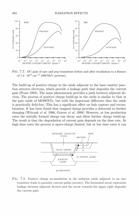
294 RADIATION EFFECTS
10-5
10-4
10-3
10-2
10-1
100
101
102
103
EM ITTER CURRENT DENSITY (µA/µm 2)
0
20
40
60
80
100
DCCURRENTGAIN
NPN
10-5
10-4
10-3
10-2
10-1
100
101
102
103
EM ITTER CURRENT DENSITY (µA/µm 2)
0
10
20
30
40
50
DCCURRENTGAIN
PNP
PRE-RAD PRE-RAD
POST-RADPOST-RAD
Fig. 7.7. DC gain of npn and pnp transistors before and after irradiation to a fluence
of 1.2 · 1014 cm−2 (800 MeV protons).
The build-up of positive charge in the oxide adjacent to the base–emitter junc-tion attracts electrons, which provide a leakage path that degrades the currentgain (Pease 1983). The same phenomenon provides a path between adjacent de-vices. The process of positive charge build-up in the oxide is similar to that inthe gate oxide of MOSFETs, but with the important difference that the oxideis practically field-free. This has a significant effect on hole capture and recom-bination. It has been found that trapped charge provides a deterrent to furthercharging (Witczak et al. 1998, Graves et al. 1998). However, at low productionrates the initially formed charge can decay and allow further charge build-up.The result is that the degradation of current gain depends on the dose rate. Athigh dose rates the process is space-charge limited, but at low dose rates it can
OXIDE CHARGE
EMITTER
BASE
np
n
n+ BURIED LAYER
p SUBSTRATE
p BURIEDLAYER
RECESSED ISOLATIONOXIDE
Fig. 7.8. Positive charge accumulation in the isolation oxide adjacent to an npn
transistor leads to parasitic current paths (arrows). The horizontal arrow represents
leakage between adjacent devices and the arrow towards the upper right degrades
the current gain.
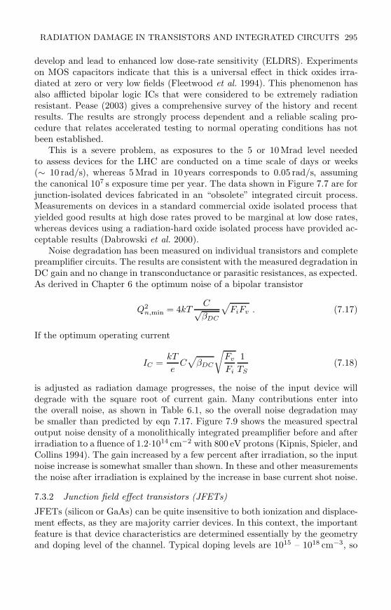
RADIATION DAMAGE IN TRANSISTORS AND INTEGRATED CIRCUITS 295
develop and lead to enhanced low dose-rate sensitivity (ELDRS). Experimentson MOS capacitors indicate that this is a universal effect in thick oxides irra-diated at zero or very low fields (Fleetwood et al. 1994). This phenomenon hasalso afflicted bipolar logic ICs that were considered to be extremely radiationresistant. Pease (2003) gives a comprehensive survey of the history and recentresults. The results are strongly process dependent and a reliable scaling pro-cedure that relates accelerated testing to normal operating conditions has notbeen established.
This is a severe problem, as exposures to the 5 or 10Mrad level neededto assess devices for the LHC are conducted on a time scale of days or weeks(∼ 10 rad/s), whereas 5 Mrad in 10years corresponds to 0.05 rad/s, assumingthe canonical 107 s exposure time per year. The data shown in Figure 7.7 are forjunction-isolated devices fabricated in an “obsolete” integrated circuit process.Measurements on devices in a standard commercial oxide isolated process thatyielded good results at high dose rates proved to be marginal at low dose rates,whereas devices using a radiation-hard oxide isolated process have provided ac-ceptable results (Dabrowski et al. 2000).
Noise degradation has been measured on individual transistors and completepreamplifier circuits. The results are consistent with the measured degradation inDC gain and no change in transconductance or parasitic resistances, as expected.As derived in Chapter 6 the optimum noise of a bipolar transistor
Q2n,min = 4kT
C√βDC
√
FiFv . (7.17)
If the optimum operating current
IC =kT
eC√
βDC
√
Fv
Fi
1
TS(7.18)
is adjusted as radiation damage progresses, the noise of the input device willdegrade with the square root of current gain. Many contributions enter intothe overall noise, as shown in Table 6.1, so the overall noise degradation maybe smaller than predicted by eqn 7.17. Figure 7.9 shows the measured spectraloutput noise density of a monolithically integrated preamplifier before and afterirradiation to a fluence of 1.2·1014 cm−2 with 800 eV protons (Kipnis, Spieler, andCollins 1994). The gain increased by a few percent after irradiation, so the inputnoise increase is somewhat smaller than shown. In these and other measurementsthe noise after irradiation is explained by the increase in base current shot noise.
7.3.2 Junction field effect transistors (JFETs)
JFETs (silicon or GaAs) can be quite insensitive to both ionization and displace-ment effects, as they are majority carrier devices. In this context, the importantfeature is that device characteristics are determined essentially by the geometryand doping level of the channel. Typical doping levels are 1015 – 1018 cm−3, so
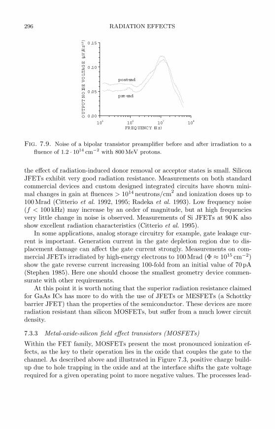
296 RADIATION EFFECTS
105
106
107
108
FREQ UENCY (Hz)
0.00
0.05
0.10
0.15
OUTPUTNOISEVOLTAGE(µV/Hz1/2)
post-rad
pre-rad
Fig. 7.9. Noise of a bipolar transistor preamplifier before and after irradiation to a
fluence of 1.2 · 1014 cm−2 with 800 MeV protons.
the effect of radiation-induced donor removal or acceptor states is small. SiliconJFETs exhibit very good radiation resistance. Measurements on both standardcommercial devices and custom designed integrated circuits have shown mini-mal changes in gain at fluences > 1014 neutrons/cm
2and ionization doses up to
100Mrad (Citterio et al. 1992, 1995; Radeka et al. 1993). Low frequency noise(f < 100 kHz) may increase by an order of magnitude, but at high frequenciesvery little change in noise is observed. Measurements of Si JFETs at 90K alsoshow excellent radiation characteristics (Citterio et al. 1995).
In some applications, analog storage circuitry for example, gate leakage cur-rent is important. Generation current in the gate depletion region due to dis-placement damage can affect the gate current strongly. Measurements on com-mercial JFETs irradiated by high-energy electrons to 100Mrad (Φ ≈ 1015 cm−2)show the gate reverse current increasing 100-fold from an initial value of 70 pA(Stephen 1985). Here one should choose the smallest geometry device commen-surate with other requirements.
At this point it is worth noting that the superior radiation resistance claimedfor GaAs ICs has more to do with the use of JFETs or MESFETs (a Schottkybarrier JFET) than the properties of the semiconductor. These devices are moreradiation resistant than silicon MOSFETs, but suffer from a much lower circuitdensity.
7.3.3 Metal-oxide-silicon field effect transistors (MOSFETs)
Within the FET family, MOSFETs present the most pronounced ionization ef-fects, as the key to their operation lies in the oxide that couples the gate to thechannel. As described above and illustrated in Figure 7.3, positive charge build-up due to hole trapping in the oxide and at the interface shifts the gate voltagerequired for a given operating point to more negative values. The processes lead-
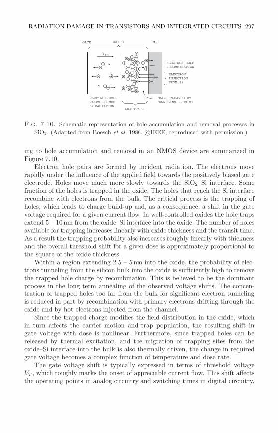
RADIATION DAMAGE IN TRANSISTORS AND INTEGRATED CIRCUITS 297
E ox
ELECTRONINJECTIONFROM Si
TRAPS CLEARED BYTUNNELING FROM Si
ELECTRON-HOLERECOMBINATION
GATE SiOXIDE
ELECTRON-HOLEPAIRS FORMEDBY RADIATION
HOLE TRAPS
Fig. 7.10. Schematic representation of hole accumulation and removal processes in
SiO2. (Adapted from Boesch et al. 1986. c©IEEE, reproduced with permission.)
ing to hole accumulation and removal in an NMOS device are summarized inFigure 7.10.
Electron–hole pairs are formed by incident radiation. The electrons moverapidly under the influence of the applied field towards the positively biased gateelectrode. Holes move much more slowly towards the SiO2–Si interface. Somefraction of the holes is trapped in the oxide. The holes that reach the Si interfacerecombine with electrons from the bulk. The critical process is the trapping ofholes, which leads to charge build-up and, as a consequence, a shift in the gatevoltage required for a given current flow. In well-controlled oxides the hole trapsextend 5 – 10nm from the oxide–Si interface into the oxide. The number of holesavailable for trapping increases linearly with oxide thickness and the transit time.As a result the trapping probability also increases roughly linearly with thicknessand the overall threshold shift for a given dose is approximately proportional tothe square of the oxide thickness.
Within a region extending 2.5 – 5 nm into the oxide, the probability of elec-trons tunneling from the silicon bulk into the oxide is sufficiently high to removethe trapped hole charge by recombination. This is believed to be the dominantprocess in the long term annealing of the observed voltage shifts. The concen-tration of trapped holes too far from the bulk for significant electron tunnelingis reduced in part by recombination with primary electrons drifting through theoxide and by hot electrons injected from the channel.
Since the trapped charge modifies the field distribution in the oxide, whichin turn affects the carrier motion and trap population, the resulting shift ingate voltage with dose is nonlinear. Furthermore, since trapped holes can bereleased by thermal excitation, and the migration of trapping sites from theoxide–Si interface into the bulk is also thermally driven, the change in requiredgate voltage becomes a complex function of temperature and dose rate.
The gate voltage shift is typically expressed in terms of threshold voltageVT , which roughly marks the onset of appreciable current flow. This shift affectsthe operating points in analog circuitry and switching times in digital circuitry.
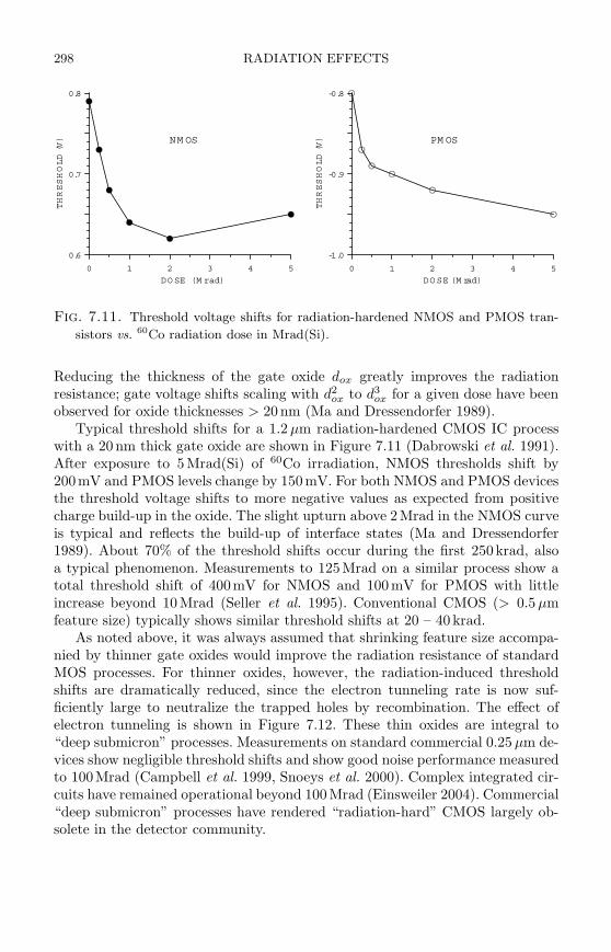
298 RADIATION EFFECTS
0 1 2 3 4 5
DO SE (M rad)
0.6
0.7
0.8
THRESHOLD(V)
0 1 2 3 4 5
DO SE (M rad)
-1.0
-0.9
-0.8
THRESHOLD(V)NM OS PM OS
Fig. 7.11. Threshold voltage shifts for radiation-hardened NMOS and PMOS tran-
sistors vs. 60Co radiation dose in Mrad(Si).
Reducing the thickness of the gate oxide dox greatly improves the radiationresistance; gate voltage shifts scaling with d2
ox to d3ox for a given dose have been
observed for oxide thicknesses > 20nm (Ma and Dressendorfer 1989).Typical threshold shifts for a 1.2 µm radiation-hardened CMOS IC process
with a 20nm thick gate oxide are shown in Figure 7.11 (Dabrowski et al. 1991).After exposure to 5Mrad(Si) of 60Co irradiation, NMOS thresholds shift by200mV and PMOS levels change by 150mV. For both NMOS and PMOS devicesthe threshold voltage shifts to more negative values as expected from positivecharge build-up in the oxide. The slight upturn above 2Mrad in the NMOS curveis typical and reflects the build-up of interface states (Ma and Dressendorfer1989). About 70% of the threshold shifts occur during the first 250krad, alsoa typical phenomenon. Measurements to 125Mrad on a similar process show atotal threshold shift of 400mV for NMOS and 100mV for PMOS with littleincrease beyond 10Mrad (Seller et al. 1995). Conventional CMOS (> 0.5 µmfeature size) typically shows similar threshold shifts at 20 – 40 krad.
As noted above, it was always assumed that shrinking feature size accompa-nied by thinner gate oxides would improve the radiation resistance of standardMOS processes. For thinner oxides, however, the radiation-induced thresholdshifts are dramatically reduced, since the electron tunneling rate is now suf-ficiently large to neutralize the trapped holes by recombination. The effect ofelectron tunneling is shown in Figure 7.12. These thin oxides are integral to“deep submicron” processes. Measurements on standard commercial 0.25 µm de-vices show negligible threshold shifts and show good noise performance measuredto 100Mrad (Campbell et al. 1999, Snoeys et al. 2000). Complex integrated cir-cuits have remained operational beyond 100Mrad (Einsweiler 2004). Commercial“deep submicron” processes have rendered “radiation-hard” CMOS largely ob-solete in the detector community.
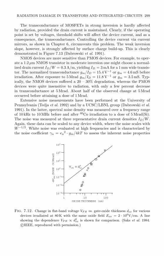
RADIATION DAMAGE IN TRANSISTORS AND INTEGRATED CIRCUITS 299
The transconductance of MOSFETs in strong inversion is hardly affectedby radiation, provided the drain current is maintained. Clearly, if the operatingpoint is set by voltages, threshold shifts will affect the device current, and as aconsequence, the transconductance. Controlling the device current via currentmirrors, as shown in Chapter 6, circumvents this problem. The weak inversionslope, however, is strongly affected by surface charge build-up. This is clearlydemonstrated in Figure 7.13 (Dabrowski et al. 1991).
NMOS devices are more sensitive than PMOS devices. For example, to oper-ate a 1.2µm NMOS transistor in moderate inversion one might choose a normal-ized drain current ID/W = 0.3 A/m, yielding ID = 3 mA for a 1 mm wide transis-tor. The normalized transconductance gm/ID = 15.4 V−1 or gm = 4.6 mS beforeirradiation. After exposure to 5Mrad gm/ID = 11.8 V−1 or gm = 3.5 mS. Typ-ically, the NMOS devices suffered a 20 – 30% degradation, whereas the PMOSdevices were quite insensitive to radiation, with only a few percent decreasein transconductance at 5Mrad. About half of the observed change at 5Mradoccurred before attaining a dose of 1Mrad.
Extensive noise measurements have been performed at the University ofPennsylvania (Tedja et al. 1992) and by a UCSC/LBNL group (Dabrowski et al.1991). In the latter, spectral noise density was measured over a frequency rangeof 10 kHz to 10MHz before and after 60Co irradiation to a dose of 5 Mrad(Si).The noise was measured at three representative drain current densities ID/W .Again, these data can be scaled to any device width, where the noise scales withW−1/2. White noise was evaluated at high frequencies and is characterized bythe noise coefficient γn = en
2 · gm/4kT to assess the inherent noise properties
OXIDE THICKNESS (nm)
-/DOSE(V/Mrad)
V
10
10
10
10
10
10
10
3
2
1
0
-1
-2
-3
FB
1 10 100
2
FB oxV d
Fig. 7.12. Change in flat-band voltage VFB vs. gate-oxide thickness dox for various
devices irradiated at 80 K with the same oxide field Eox = 2 · 106V/cm. A line
showing the dependence VFB ∝ d2ox is shown for comparison. (Saks et al. 1984.
c©IEEE, reproduced with permission.)
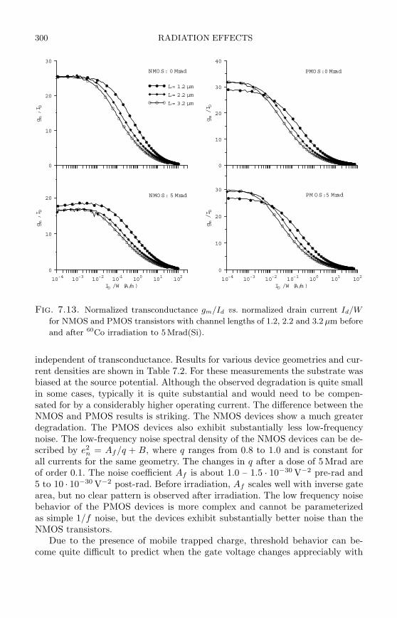
300 RADIATION EFFECTS
NMO S: 5 Mrad
NMO S: 0 Mrad PMO S: 0 Mrad
PM OS: 5 Mrad
0
10
20
30
gm/I D
10-4
10-3
10-2
10-1
100
101
102
ID /W (A/m )
0
10
20
gm/I D
10-4
10-3
10-2
10-1
100
101
102
ID /W (A/m )
0
10
20
30
gm/I D
L= 1.2 µm
L= 2.2 µm
L= 3.2 µm
0
10
20
30
40
gm/I D
Fig. 7.13. Normalized transconductance gm/Id vs. normalized drain current Id/W
for NMOS and PMOS transistors with channel lengths of 1.2, 2.2 and 3.2 µm before
and after 60Co irradiation to 5 Mrad(Si).
independent of transconductance. Results for various device geometries and cur-rent densities are shown in Table 7.2. For these measurements the substrate wasbiased at the source potential. Although the observed degradation is quite smallin some cases, typically it is quite substantial and would need to be compen-sated for by a considerably higher operating current. The difference between theNMOS and PMOS results is striking. The NMOS devices show a much greaterdegradation. The PMOS devices also exhibit substantially less low-frequencynoise. The low-frequency noise spectral density of the NMOS devices can be de-scribed by e2
n = Af/q + B, where q ranges from 0.8 to 1.0 and is constant forall currents for the same geometry. The changes in q after a dose of 5 Mrad areof order 0.1. The noise coefficient Af is about 1.0 – 1.5 · 10−30 V−2 pre-rad and5 to 10 · 10−30 V−2 post-rad. Before irradiation, Af scales well with inverse gatearea, but no clear pattern is observed after irradiation. The low frequency noisebehavior of the PMOS devices is more complex and cannot be parameterizedas simple 1/f noise, but the devices exhibit substantially better noise than theNMOS transistors.
Due to the presence of mobile trapped charge, threshold behavior can be-come quite difficult to predict when the gate voltage changes appreciably with
RADIATION DAMAGE IN TRANSISTORS AND INTEGRATED CIRCUITS 301
varying duty cycles, as in logic circuitry. Detectors and analog circuitry are sim-pler by comparison, since the voltage levels are either static or change with afixed period, as in analog pipelines, for example. In general, when performingionization damage tests devices must be operated at typical operating voltagesand digital circuitry must be clocked at frequencies and patterns approximatingtypical operation.
Generally speaking, both bulk and SOI (silicon on insulator) CMOS are sub-ject to the effects described above. SOI is often cited as a specifically radiation-hard technology because of its resistance to transient radiation effects, primarilylatchup due to photocurrents developed at high intensity bursts of radiation(> 106 − 107 rad/s) typical of nuclear detonations (latchup is explained in Ap-pendix A). Although SOI can provide superior device speed because of reducedstray capacitance, this technology is not inherently more resistant to radiation inour applications. If anything, the additional oxide interfaces tend to complicatematters and at this time most radiation-resistant CMOS processes are on bulksilicon.
Table 7.2 Noise coefficients γn = e2n · gm/4kT for NMOS and PMOS transistors
of various widths and lengths, operated at current densities Id/W = 0.03, 0.10 and0.3 A/m, before and after 60Co irradiation to 5 Mrad(Si).
Type NMOS PMOS NMOS PMOS NMOS PMOS NMOS PMOS
Width (µm) 75 75 1332 1332 888 888 1332 1332
Length (µm) 1.2 1.2 1.2 1.2 2.2 2.2 3.2 3.2
Id/W = 0.03
0 Mrad 0.81 0.61 0.64 0.59 0.66 0.5
5 Mrad 2.17 0.84 1.00 0.58 1.50 0.69
Id/W = 0.1
0 Mrad 1.10 0.70 1.20 1.10 0.80 0.80 0.80 0.66
5 Mrad 3.80 1.10 3.40 1.60 1.30 0.90 1.70 0.70
Id/W = 0.3
0 Mrad 1.60 1.30 2.00 1.70 1.10 1.00 1.10 0.77
5 Mrad 5.00 2.90 4.80 2.70 1.60 1.40 1.20 0.81
302 RADIATION EFFECTS
7.3.4 Radiation effects in integrated circuit structures
The preceding discussion has emphasized the properties of individual devices. Inintegrated circuits many devices are placed close together. As mentioned above,the silicon surface is naturally n-type, so isolation structures are required topreclude unwanted cross-coupling between devices. Two basic techniques areused:
• junction isolation, where reverse-biased pn-junctions provide both ohmicand capacitive isolation.
• oxide isolation, where oxide layers with carefully controlled interface prop-erties deplete the adjacent silicon of mobile charge.
Detailed information on these processes can be found in texts on IC technology,for example in the comprehensive series by Wolf (1990, 1995, 2002).
Junction isolation is very robust, but requires substantial additional space.Oxide isolation allows higher packing densities and is used by most high-densityIC processes. All CMOS processes utilize some form of oxide isolation, whereasbipolar transistor processes can be found with both junction and oxide isola-tion. Under irradiation the oxide layers used for isolation (field oxide) sufferfrom the same phenomena described for the gate oxide of MOSFETs (see fieldoxide in Figure 7.3). Since isolation oxides are thicker than gate oxides, moreelectron–hole pairs are formed by incident radiation. Furthermore, the fields inthe isolation oxide tend to be much lower, so charge trapping in the oxide willbe exacerbated. Developing radiation-hard isolation oxides (field oxides) was amajor challenge in the development of high-density radiation-hard CMOS andremains one of the few “secret” process ingredients (for a basic discussion seeMa and Dressendorfer 1989). In commercial “deep submicron” processes NMOSleakage is the main problem. This is eliminated by using enclosed geometry tran-sistors and p+ guard rings. A small drain is surrounded by the gate, which is inturn enclosed by the source (Snoeys et al. 2000).
Inherently radiation-hard devices, notably JFETs and bipolar transistors,are often implemented in nonhardened oxide-isolated processes. Here radiationeffects in the isolation structures can severely affect the radiation resistance ofthe devices. Clues to the importance of such parasitic ionization effects can begleaned from a comparison of neutron and photon irradiations. As discussed inthe context of low dose rate effects in bipolar transistor ICs, the suitability ofthese processes must be determined case-by-case.
IC processes also use special device structures to facilitate the integration ofdifferent device types. A prime example is the lateral pnp transistor, a structuremore compatible with a standard CMOS process than “classic” vertical bipolartransistors. In a lateral transistor the emitter, base and collector are arrangedalong the surface of the silicon with large-area exposure to oxide interfaces.Unlike vertical bipolar transistors, lateral devices are very susceptible to ionizingradiation, as surface leakage causes severe degradation of DC gain. Lateral pnp
DOSIMETRY 303
transistors can be used as current sources or high impedance loads, if the biasingcircuitry is designed to accommodate substantial increases in base currents.
Digital circuitry is susceptible to single event upset. In modern devices thecharge required to change the state of a switching device is so small that it can beintroduced by local charge deposition from single particles. It is more probable forheavily ionizing particles (alphas, for example), but minimum ionizing particlescan produce Si recoils that have a significantly higher energy loss dE/dx. Thisleads to “soft errors” that can be detected by appropriate error codes. CMOScircuitry includes parasitic bipolar transistors that can form a p-n-p-n thyristorstructure (Appendix A). This structure can latch up in a nonrecoverable state.The probability of single event processes can be minimized by appropriate processand circuit design. For a survey see Holmes-Siedle and Adams (2002). As anexample, see the investigation of single event upset in optical links for the ATLASsilicon strip detector by Dowell et al. (2002).
7.4 Dosimetry
Dosimetry is fairly straightforward in irradiations with charged particles, but isoften flawed in 60Co irradiations used in assessing ionization effects. The absorp-tion length of the ∼ 1 MeV photons emitted in 60Co decays is ∼ 5 cm (Figure1.20), much greater than the depth of the devices to be tested. As MOSFETsand oxide layers are at the surface, very few photons are absorbed in the de-vice structures to be tested. However, photons scattered from the surroundings(concrete walls or packaging materials, for example) excite x-rays with a high ab-sorption probability (dose enhancement, see Ma and Dressendorfer 1989, Srouret al. 1984). As a consequence, the dose in 60Co irradiations may be substantiallyhigher or lower than estimated from source activity alone. Reproducible circum-stances are established by ensuring “charge transfer equilibrium”. As Comptonscattering dominates, the deposited dose is due to the energy deposited by theCompton electrons. By enclosing the sample with material that ensures thatthe flux of Compton electrons entering the sample equals the flux exiting thesample, the dose is uniform and well-established throughout the sample. Ideally,the absorber would be silicon, but this is quite cumbersome, so higher densitymaterials such as lead are used. However, the x-rays from the non-silicon ab-sorber can lead to dose enhancement, so to suppress them an additional layerof aluminum is included, adjacent to the sample. This creates a “silicon-like”environment, as the Al and Si x-rays are of similar energy. A suitable equilib-rium shield consists 1.5mm of lead followed by 0.7mm of aluminum (Ma andDressendorfer 1989). X-ray generators are convenient for use in radiation test-ing, but the strong dependence of absorption on depth for the typical energyspectra make dosimetry very difficult. Nevertheless, they can be quite effectivein comparative measurements or process monitoring.
304 RADIATION EFFECTS
7.5 Mitigation techniques
Although within a given technology little can be done to reduce radiation damageto an individual device, many techniques can be applied to reduce the effects ofradiation damage to an overall system. The goal of radiation-hard design is not somuch to obtain a system whose characteristics do not change under irradiation,rather than to maintain the required performance characteristics over the lifetimeof the system. The former approach tends to utilize mediocre to poor technologiesthat remain so over the course of operation. The latter starts out with superiorcharacteristics, which gradually deteriorate under irradiation. Depending on thespecific system, these designs may “die” gradually, although at some fluence ordose a specific circuit, typically digital, may cease to function at all.
7.5.1 Detectors
Increased detector leakage current has several undesirable consequences.
1. The integrated current over typical signal processing times can greatlyexceed the signal.
2. Shot noise increases.
3. The power dissipated in the detectors increases (bias current times voltage).
Since the leakage current decreases exponentially with temperature, cooling isthe simplest technique to reduce diode leakage current. For example, reducingthe detector temperature from room temperature to 0 C reduces the bias currentto about 1/6 of its original value.
Detector power dissipation is a concern in large-area silicon detectors forthe LHC, where the power dissipation in the detector diode itself can be oforder 1 – 10mW/cm2. Since the leakage current is an exponential function oftemperature, local heating will increase the leakage current, which will increasethe local heating, and so on, ultimately taking the device into thermal runaway.To avoid this potentially catastrophic failure mode, the cooling system must bedesigned to provide sufficient cooling of the detector, a challenging (but doable)task in a system that is to have zero mass. An implementation and results areshown in the next chapter, Section 8.6.5.
Reducing the integration time reduces both baseline changes due to inte-grated detector current and shot noise. Clearly, this is limited by the durationof the signal to be measured. To some degree, circuitry can be designed to ac-commodate large baseline shifts due to detector current, but at the expense ofpower. AC coupled detectors eliminate this problem. In instrumentation systemsthat require DC coupling, correlated double sampling techniques can be used tosample the baseline before the signal occurs and then subtract from the signalmeasurement.
One of the most powerful measures against detector leakage current is seg-mentation. For a given damage level, the detector leakage current per signalchannel can be reduced by segmentation. If a diode with a leakage current of10 µA is subdivided into 100 subelectrodes each with its own signal processing
MITIGATION TECHNIQUES 305
channel, the bias current in each channel will be 100nA and shot noise reducedby a factor of 10. This is why large area silicon tracking detectors can survivein the LHC environment. Fortuitously, increased segmentation is also requiredto deal with the high event rate. Pixel detectors with small electrode areas offergreat advantages in this regard.
The most severe restriction on radiation resistance is imposed by type inver-sion in the sensor, when the net space charge becomes so large that the detectorwill no longer sustain the required voltage for full charge collection. This isespecially critical for position-sensing detectors with electrodes on both sides(double-sided detectors), for which full collection is essential (see Section 2.5.3).
One can circumvent the type-inversion limit by using back-to-back single-sided detectors. The initial configuration uses n-type segmented strip electrodeson n bulk, with a contiguous p electrode on the backside. Initially, the pn-junctionis at the backside. This does require full depletion in initial operation, but thisis no problem for the nonirradiated device and becomes easier to maintain asincreasing fluence moves the bulk towards type inversion. After type inversion thecharge collection region extends from the n electrodes. Since most of the signalcharge is induced when the carriers are near the strip or pixel electrodes, thisprovides good efficiency even when operating at less than “depletion” voltage(Unno et al. 1996, 1997).
Since highly damaged detectors are largely devoid of mobile charge, they ap-pear approximately ohmic. This means that reverse bias is not essential to obtainlow acceptable bias currents and the detectors also function under forward bias.Chilingarov and Sloan (1997b) demonstrated good charge collection efficiencywith forward bias voltages much smaller than the reverse bias required for thesame signal. Although the bias current is larger than for reverse bias, this resultsin less power dissipation in the detector and also simplifies the detector design.However, the smaller fields also lead to longer collection times, so the effect oftrapping is exacerbated. To some degree this is ameliorated by the fact thatelectron traps are more readily filled by the larger standing current (Beattie etal. 2000).
A innovative approach to avoiding large operating voltages while reducingcollection times is the “3D detector” (Parker, Kenney, and Segal 1997). Ratherthan forming the diode between opposite faces of a wafer, the electrodes arealternating columns of n+ and p+ material that are are normal to the surface ofthe p bulk. Columns have been implemented with 300µm depth and a diameterabout 5% of the depth (Kenney et al. 1999). In one set of test devices the pitchwithin a row is 200 µm and adjacent n- and p-rows are offset by 100 µm so that thedistance that must be depleted is ∼ 140 µm. By appropriate choice of geometrythe distance between n- and p-columns can be much smaller than the waferthickness, so that both the required voltage for full collection and the collectiontimes are reduced. For example, a spacing of 50µm betwen n- and p-columnswould yield full charge collection at order of magnitude smaller voltage thanconventional devices. Devices have been irradiated to fluences > 5 · 1014 cm−2
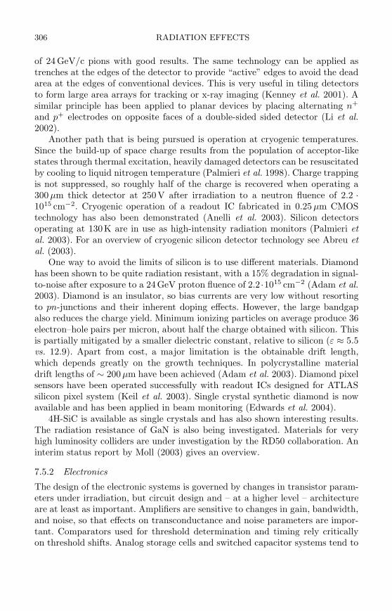
306 RADIATION EFFECTS
of 24 GeV/c pions with good results. The same technology can be applied astrenches at the edges of the detector to provide “active” edges to avoid the deadarea at the edges of conventional devices. This is very useful in tiling detectorsto form large area arrays for tracking or x-ray imaging (Kenney et al. 2001). Asimilar principle has been applied to planar devices by placing alternating n+
and p+ electrodes on opposite faces of a double-sided sided detector (Li et al.2002).
Another path that is being pursued is operation at cryogenic temperatures.Since the build-up of space charge results from the population of acceptor-likestates through thermal excitation, heavily damaged detectors can be resuscitatedby cooling to liquid nitrogen temperature (Palmieri et al. 1998). Charge trappingis not suppressed, so roughly half of the charge is recovered when operating a300 µm thick detector at 250V after irradiation to a neutron fluence of 2.2 ·1015 cm−2. Cryogenic operation of a readout IC fabricated in 0.25 µm CMOStechnology has also been demonstrated (Anelli et al. 2003). Silicon detectorsoperating at 130K are in use as high-intensity radiation monitors (Palmieri etal. 2003). For an overview of cryogenic silicon detector technology see Abreu etal. (2003).
One way to avoid the limits of silicon is to use different materials. Diamondhas been shown to be quite radiation resistant, with a 15% degradation in signal-to-noise after exposure to a 24GeV proton fluence of 2.2 ·1015 cm−2 (Adam et al.2003). Diamond is an insulator, so bias currents are very low without resortingto pn-junctions and their inherent doping effects. However, the large bandgapalso reduces the charge yield. Minimum ionizing particles on average produce 36electron–hole pairs per micron, about half the charge obtained with silicon. Thisis partially mitigated by a smaller dielectric constant, relative to silicon (ε ≈ 5.5vs. 12.9). Apart from cost, a major limitation is the obtainable drift length,which depends greatly on the growth techniques. In polycrystalline materialdrift lengths of ∼ 200 µm have been achieved (Adam et al. 2003). Diamond pixelsensors have been operated successfully with readout ICs designed for ATLASsilicon pixel system (Keil et al. 2003). Single crystal synthetic diamond is nowavailable and has been applied in beam monitoring (Edwards et al. 2004).
4H-SiC is available as single crystals and has also shown interesting results.The radiation resistance of GaN is also being investigated. Materials for veryhigh luminosity colliders are under investigation by the RD50 collaboration. Aninterim status report by Moll (2003) gives an overview.
7.5.2 Electronics
The design of the electronic systems is governed by changes in transistor param-eters under irradiation, but circuit design and – at a higher level – architectureare at least as important. Amplifiers are sensitive to changes in gain, bandwidth,and noise, so that effects on transconductance and noise parameters are impor-tant. Comparators used for threshold determination and timing rely criticallyon threshold shifts. Analog storage cells and switched capacitor systems tend to
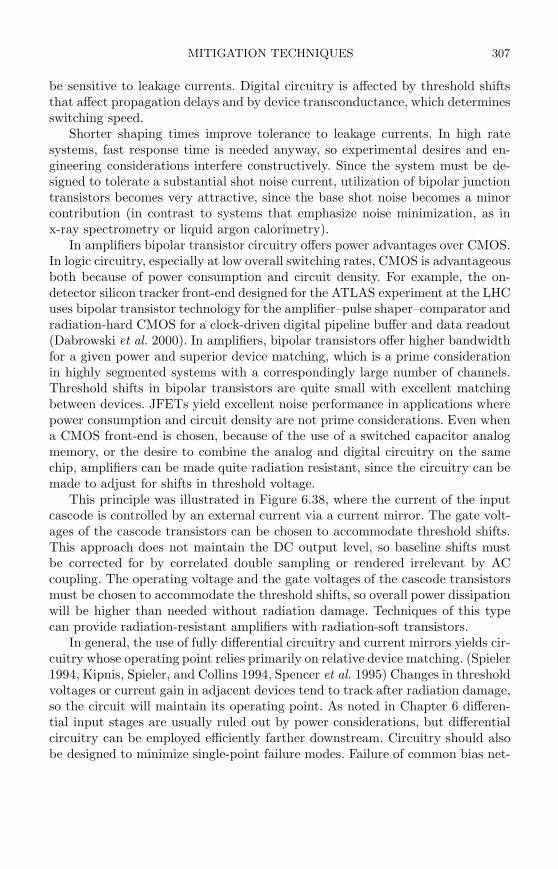
MITIGATION TECHNIQUES 307
be sensitive to leakage currents. Digital circuitry is affected by threshold shiftsthat affect propagation delays and by device transconductance, which determinesswitching speed.
Shorter shaping times improve tolerance to leakage currents. In high ratesystems, fast response time is needed anyway, so experimental desires and en-gineering considerations interfere constructively. Since the system must be de-signed to tolerate a substantial shot noise current, utilization of bipolar junctiontransistors becomes very attractive, since the base shot noise becomes a minorcontribution (in contrast to systems that emphasize noise minimization, as inx-ray spectrometry or liquid argon calorimetry).
In amplifiers bipolar transistor circuitry offers power advantages over CMOS.In logic circuitry, especially at low overall switching rates, CMOS is advantageousboth because of power consumption and circuit density. For example, the on-detector silicon tracker front-end designed for the ATLAS experiment at the LHCuses bipolar transistor technology for the amplifier–pulse shaper–comparator andradiation-hard CMOS for a clock-driven digital pipeline buffer and data readout(Dabrowski et al. 2000). In amplifiers, bipolar transistors offer higher bandwidthfor a given power and superior device matching, which is a prime considerationin highly segmented systems with a correspondingly large number of channels.Threshold shifts in bipolar transistors are quite small with excellent matchingbetween devices. JFETs yield excellent noise performance in applications wherepower consumption and circuit density are not prime considerations. Even whena CMOS front-end is chosen, because of the use of a switched capacitor analogmemory, or the desire to combine the analog and digital circuitry on the samechip, amplifiers can be made quite radiation resistant, since the circuitry can bemade to adjust for shifts in threshold voltage.
This principle was illustrated in Figure 6.38, where the current of the inputcascode is controlled by an external current via a current mirror. The gate volt-ages of the cascode transistors can be chosen to accommodate threshold shifts.This approach does not maintain the DC output level, so baseline shifts mustbe corrected for by correlated double sampling or rendered irrelevant by ACcoupling. The operating voltage and the gate voltages of the cascode transistorsmust be chosen to accommodate the threshold shifts, so overall power dissipationwill be higher than needed without radiation damage. Techniques of this typecan provide radiation-resistant amplifiers with radiation-soft transistors.
In general, the use of fully differential circuitry and current mirrors yields cir-cuitry whose operating point relies primarily on relative device matching. (Spieler1994, Kipnis, Spieler, and Collins 1994, Spencer et al. 1995) Changes in thresholdvoltages or current gain in adjacent devices tend to track after radiation damage,so the circuit will maintain its operating point. As noted in Chapter 6 differen-tial input stages are usually ruled out by power considerations, but differentialcircuitry can be employed efficiently farther downstream. Circuitry should alsobe designed to minimize single-point failure modes. Failure of common bias net-
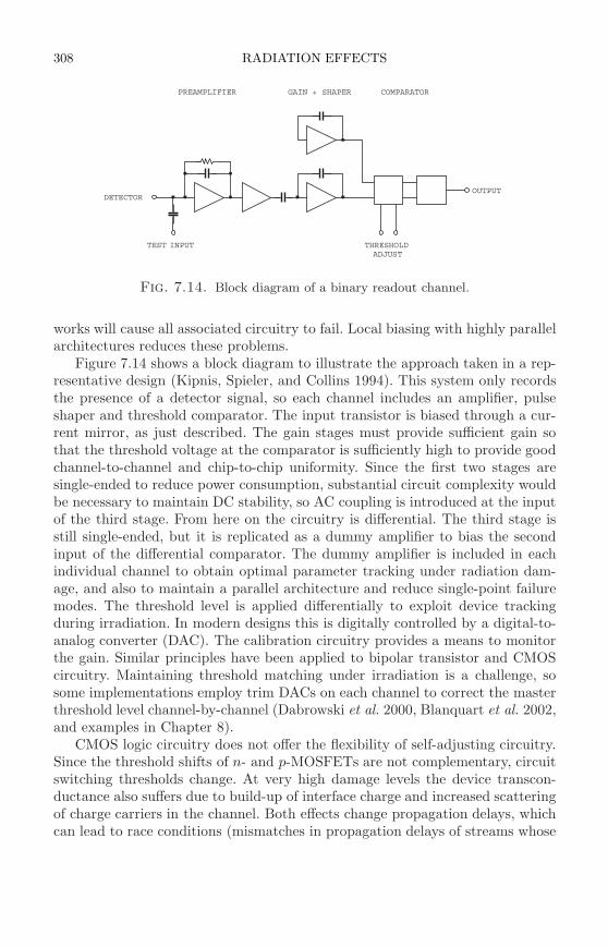
308 RADIATION EFFECTS
PREAMPLIFIER GAIN + SHAPER COMPARATOR
OUTPUTDETECTOR
TEST INPUT THRESHOLDADJUST
Fig. 7.14. Block diagram of a binary readout channel.
works will cause all associated circuitry to fail. Local biasing with highly parallelarchitectures reduces these problems.
Figure 7.14 shows a block diagram to illustrate the approach taken in a rep-resentative design (Kipnis, Spieler, and Collins 1994). This system only recordsthe presence of a detector signal, so each channel includes an amplifier, pulseshaper and threshold comparator. The input transistor is biased through a cur-rent mirror, as just described. The gain stages must provide sufficient gain sothat the threshold voltage at the comparator is sufficiently high to provide goodchannel-to-channel and chip-to-chip uniformity. Since the first two stages aresingle-ended to reduce power consumption, substantial circuit complexity wouldbe necessary to maintain DC stability, so AC coupling is introduced at the inputof the third stage. From here on the circuitry is differential. The third stage isstill single-ended, but it is replicated as a dummy amplifier to bias the secondinput of the differential comparator. The dummy amplifier is included in eachindividual channel to obtain optimal parameter tracking under radiation dam-age, and also to maintain a parallel architecture and reduce single-point failuremodes. The threshold level is applied differentially to exploit device trackingduring irradiation. In modern designs this is digitally controlled by a digital-to-analog converter (DAC). The calibration circuitry provides a means to monitorthe gain. Similar principles have been applied to bipolar transistor and CMOScircuitry. Maintaining threshold matching under irradiation is a challenge, sosome implementations employ trim DACs on each channel to correct the masterthreshold level channel-by-channel (Dabrowski et al. 2000, Blanquart et al. 2002,and examples in Chapter 8).
CMOS logic circuitry does not offer the flexibility of self-adjusting circuitry.Since the threshold shifts of n- and p-MOSFETs are not complementary, circuitswitching thresholds change. At very high damage levels the device transcon-ductance also suffers due to build-up of interface charge and increased scatteringof charge carriers in the channel. Both effects change propagation delays, whichcan lead to race conditions (mismatches in propagation delays of streams whose
REFERENCES 309
results are combined) that cause circuit failure. These problems require carefuldesign. On the other hand, digital circuitry can be used to control operatingpoints and enhance radiation resistance by adjusting for changes in analog cir-cuitry. Examples are shown in Chapter 8.
7.5.3 Summary
Judicious evaluation of the radiation fields coupled with a stringent analysisof application requirements have yielded electronic systems that perform wellto ionizing doses of 100Mrad and particle fluences of to 1015 cm−2. Some ex-amples will be discussed in Chapter 8. Developing radiation-resistant systemsdoes require great attention to detail and substantially more testing effort thanconventional designs, but the effort is necessary to support the need for everincreasing luminosity. For many applications we are limited less by technologythan by ingenuity.
References
Abreu, M. et al. (2003). Recent progress in low-temperature silicon detectors.Nucl. Phys. B (Proc. Suppl) 125 (2003) 169–174
Adam, W. et al. (2003). The development of diamond tracking detectors forthe LHC. Nucl. Instr. and Meth. A514 79–86
Anelli, G. et al. (2003). A high-speed low-noise transimpedance amplifier in a0.25 µm CMOS technology. Nucl. Instr. and Meth. A512 (2003) 117–128
Azzi, P. et al. (1996). Radiation damage experience at CDF with SVX’. Nucl.Instr. and Meth. A383 (1996) 155–158
Barberis, E. et al. (1993). Temperature effects on radiation damage to silicondetectors. Nucl. Instr. and Meth. A326 (1993) 373–380
Barberis, E. et al. (1994). Capacitances in silicon microstrip detectors. Nucl.Instr. and Meth. A342 (1994) 90–95
Beattie, L.J. et al. (1998) The electric field in irradiated silicon detectors. Nucl.Instr. and Meth. A418 (1998) 314–321
Beattie, L.J. et al. (2000). Forward-bias operation of Si detectors: a way to workin high-radiation environment. Nucl. Instr. and Meth. A439 (2000) 293–302
Blanquart, L. et al. (2002). Analog front-end cell designed in a commercial0.25 µm process for the ATLAS pixel detector at LHC. IEEE Trans.Nucl.Sci.49 (2002) 1778–1782
Boesch, H.E. et al. (1986). Saturation of threshold voltage shift in MOSFETsat high total dose. IEEE Trans. Nucl. Sci. NS-33/6 (1986) 1191–1197
Borgeaud, P. et al. (1983). The effect of radiation on the energy resolution ofion-implanted silicon detectors. Nucl. Instr. and Meth. 211 (1983) 363–367
Brodbeck, T.J. et al. (2002). Carrier mobilities in irradiated silicon. Nucl. Instr.and Meth. A477 (2002) 287–292
Burke E.A. (1986). Energy Dependence of proton-induced displacement damagein silicon. IEEE Trans. Nucl. Sci. NS-33/6 (1986) 1276–1281
310 RADIATION EFFECTS
Campbell, M. et al. (1999). A pixel readout chip for 10–30 Mrad in standard0.25µm CMOS. IEEE Trans. Nucl. Sci. NS-46/3 (1999) 156–160
Cartiglia, N. et al. (1992). Radiation hardness measurements on bipolar teststructures and an amplifier-comparator Circuit. Conference Record of the IEEENuclear Science Symposium, Oct. 25–31, 1992, Orlando, Florida. Vol. 2, pp.819–821. ISBN 0-7803-0883-2
Castaldini, A. et al. (2002). Electric field distribution in irradiated silicon de-tectors. Nucl. Instr. and Meth. A476 (2002) 550–555
A. Chilingarov et al. (1995). Radiation effects and operational projections forsilicon in the ATLAS inner detector. Nucl. Instr. and Meth. A360 (1995) 432
A. Chilingarov, Meyer, J.S. and Sloan, T. (1997a). Radiation damage due toNIEL in GaAs particle detectors. Nucl. Instr. and Meth. A395 (1997) 35–44
A. Chilingarov, A. and Sloan, T. (1997b). Operation of heavily irradiated silicondetectors under forward bias. Nucl. Instrum. and Meth. A399 (1997) 35–37
Citterio, M. et al. (1992). A Study of low noise JFETs exposed to large dosesof gamma rays and neutrons. Conference Record of the IEEE Nuclear ScienceSymposium, Oct. 25–31, 1992, Orlando, Florida. Vol. 2, pp. 794–796. ISBN0-7803-0883-2
Citterio, M. et al. (1995). Radiation effects at cryogenic temperatures in Si-JFET, GaAs MESFET, and MOSFET devices. IEEE Trans. Nucl. Sci. NS-42/6 (1995) 2266–2270
Dabrowski, W. et al. (1991). Noise measurements on radiation-hardened CMOStransistors. Conference Record of the 1991 IEEE Nuclear Science Symposiumand Medical Imaging Conference, Nov. 2–9, 1991, Santa Fe, New Mexico. Vol.3, pp. 1536–1540. IEEE catalog no. 91CH3100-5
Dabrowski, W. et al. (2000). Design and performance of the ABCD chip for thebinary readout of silicon strip detectors in the ATLAS semiconductor tracker.IEEE Trans.Nucl.Sci. NS-47 (2000) 1843–1850
Dowell, J.D. et al. (2002). Single event upset studies with the optical linksof the ATLAS semiconductor tracker. Nucl.Instrum. and Meth. A481 (2002)575–584
Edwards, A.J. et al. (2004). Radiation monitoring with diamond sensors inBaBar. IEEE Trans. Nucl. Sci. 51/4 1808–1811
Einsweiler, K. (1994). private communicationEremin, V., Verbitskaya, E. and Li, Z. (2002). The origin of double peak electricfield distribution in heavily irradiated silicon detectors. Nucl. Instr. and Meth.A476 (2002) 556–564
Fleetwood, D.M. et al. (1994) Physical mechanisms contributing to enhancedbipolar gain degradation at low dose rates. IEEE Trans. Nucl. Sci. NS-411871–1883
Gill, K. et al. (1992). Radiation damage by neutrons and photons to silicondetectors. Nucl. Instr. and Meth. A322 (1992) 177
Giubellino, P. et al. (1992). Study of the effects of neutron irradiation on siliconstrip detectors. Nucl. Instr. and Meth. A315 (1992) 156
REFERENCES 311
Graves, R.J. et al. (1998). Modeling low dose rate effects in irradiated bipolaroxides.IEEE Trans. Nucl. Sci. NS-45 (1998) 2352–2365
Griffin, P.J. et al. (1993). Sandia National Laboratories Report SAND92-0094Grosse-Knetter, J. for the ATLAS Pixel Collaboration (2004). The ATLAS pixeldetector. e-Print Archive: physics/0401068,http://arxiv.org/PS cache/physics/pdf/0401/0401068.pdf
Grove, A.S. (1967). Physics and Technology of Semiconductor Devices. Wiley,New York. ISBN 0-471-32998-3
Holmes-Siedle, A. and Adams, L. (2002). Handbook of Radiation Effects (2ndedn). Oxford University Press, Oxford. ISBN 0-19-850733-X, QC474.H59
Huhtinen, M. and Aarnio, P.A. (1993). Pion induced displacement damage insilicon devices. Nucl. Instr. and Meth. A335 (1993) 580–582
Huhtinen, M. (2002). Simulation of non-ionizing energy loss and defect forma-tion in silicon. Nucl. Instr. and Meth. A491 (2002) 194–215
Keil, M. et al. (2003). New results on diamond pixel sensors using ATLASfrontend electronics. Nucl. Instr. and Meth. A501 153–159
Kenney, C. et al. (1999). Silicon detectors with 3-D electrode arrays: fabricationand initial test results. IEEE Trans. Nucl. Sci. NS-46/4 (1999) 1224–1236
Kenney, C.J. et al. (2001). Observation of beta and X rays with 3D-architecturesilicon microstrip sensors. IEEE Trans. Nucl. Sci. NS-48/2 (2001) 189–193
Kipnis, I., Spieler, H. and Collins, T. (1994). An analog front-end bipolar-transistor integrated circuit for the SDC silicon tracker. IEEE Trans. Nucl.Sci. NS-41/4 (1994) 1095–1103
Kondo, T. et al. (1984) Radiation damage test of silicon microstrip detectors.Proceedings of the 1984 Summer Study on the Design and Utilization of theSuperconducting Super Collider, Snowmass, CO, Jun 23 – Jul 13, 1984. (eds.R. Donaldson, J.C. Morfin) pp. 612–614. QCD184 S7 1984
Konobeyev, A. (1992). Neutron displacement cross-sections for structural ma-terials below 800MeV. J. Nucl. Mat. 186 (1992) 117–130
Kramberger, G. et al. (2002). Effective trapping time of electrons and holes indifferent silicon materials irradiated with neutrons, protons and pions. Nucl.Instr. and Meth. A481 (2002) 297–305
Kraner, H.W. (1982). Radiation damage in semiconductor detectors. IEEETrans. Nucl. Sci. NS-29/3 (1982) 1088–1100
Krasel, O. et al. (2004). Measurement of trapping time constants in proton-irradiated silicon pad detectors. IEEE Trans. Nucl. Sci. NS-51/6 (2004)3055–3062
Kubota, M. et al. (1991). Radiation damage of double-sided silicon strip de-tectors. Conference Record of the 1991 IEEE Nuclear Science Symposium andMedical Imaging Conference, Nov. 2 – 9, 1991, Santa Fe, New Mexico. Vol. 1,p. 246
Kuznetsov, V.I. et al. (1975). Inversion of the type of conduction and stabiliza-tion of the Fermi level in irradiated silicon. Sov. Phys. Semicond. 9/4 (1975)491–492, Fiz. Tekh. Poluprovodn. 9 (1975) 749–752
312 RADIATION EFFECTS
Lemeilleur, F. et al. (1982). Neutron-induced radiation damage in silicon detec-tors. IEEE Trans. Nucl. Sci. NS-39/4 (1992) 551–557
Li, Z. al (1992). Investigation of the oxygen-vacancy (A-center) defect complexprofile in neutron irradiated high resistivity silicon junction particle detectors.IEEE Trans. Nucl. Sci. 39/6 (1992) 1730–1738
Li, Z. (1994). Modeling and simulation of neutron induced changes and tem-perature annealing of Neff and changes in resistivity in high resistivity silicondetectors. Nucl. Instr. and Meth. A342 (1994) 105–118
Li, Z. et al. (2002). Novel prototype Si detector development and processing atBNL. Nucl. Instr. and Meth. A478 (2002) 303–310
Lindstrom, G., Moll, M. and Fretwurst, E. (1999). Radiation hardness of silicondetectors – a challenge from high-energy physics. Nucl. Instr. and Meth. A426(1999) 1–15
Lindstrom, G. (2000). Displacement Damage in Silicon.http://sesam.desy.de/members/gunnar/Si-dfuncs.html
Lindstrom, G. for the RD48 Collaboration (2001). Radiation hard silicon de-tectors – developments by the RD48 (ROSE) collaboration. Nucl. Instr. andMeth. A466 (2001) 308–326
Messenger, G.C. and Ash, M.S. (1986) The Effects of Radiation on ElectronicSystems. van Nostrand Reinhold, New York. ISBN 0-442-25417-2,TK7870.M4425
Messenger, S.R. et al. (2004). Limits to the application of NIEL for damagecorrelation. IEEE Trans. Nucl. Sci. NS-51/6 (2004) 3201–3206
Ma, T.P. and P.V. Dressendorfer (1989). Ionizing Radiation Effects in MOS De-vices and Circuits. Wiley, New York, ISBN 0-471-84893-X, TK7871.99.M44I56
Moll, M. (1999) Radiation Damage in Silicon Particle Detectors. PhD the-sis, University of Hamburg, 1999. DESY THESIS-1999-040, ISSN-1435-8085.Available at http://mmoll.home.cern.ch/mmoll/thesis/
Moll, M. (2003). Development of radiation hard sensors for very high luminositycolliders – CERN-RD50 project. Nucl. Instr. and Meth. A511 (2003) 97–105
Oldham, T. (1999). Ionizing Radiation Effects in MOS Oxides. World Scientific,Singapore. ISBN 981-02-3326-4
Ohsugi, T. et al. (1988). Radiation damage in silicon microstrip detectors. Nucl.Instr. and Meth. A265 (1988) 105–111
Palmieri, G.P. et al. (1998). Evidence for charge collection recovery in heavilyirradiated silicon detectors operated at cryogenic temperatures. Nucl. Instr.and Meth. A413 (1998) 475–478
Palmieri, V.G. et al. (2003). Cryogenic semiconductor high-intensity radiationmonitors. Nucl. Instrum. and Meth. A510 (2003) 97–100
Parker, S., Kenney, C.J. and Segal, J. (1997). 3-D: a new architecture for solid-state radiation detectors. Nucl. Instrum. and Meth. A395 (1997) 328–343
Pease, R.L. (1983). Total dose effects in recessed oxide digital bipolar microcir-cuits. IEEE Trans. Nucl. Sci. NS-30 (1983) 4216–4223
REFERENCES 313
Pease, R.L. (2003). Total ionizing dose effects in bipolar devices and circuits.IEEE Trans. Nucl. Sci. NS-50/3 (2003) 539–551
Pitzl, D. et al. (1992). Type inversion in silicon detectors. Nucl. Instr. and Meth.A311 (1992) 98–104
Radeka, V. et al. (1993). JFET monolithic preamplifier with outstanding noisebehavior and radiation hardness characteristics. IEEE Trans. Nucl. Sci. NS-40/4 (1993) 744–749
RD48 (1999), 3rd Status Report. CERN/LHCC 2000-0089.http://rd48.web.cern.ch/rd48/
Rogalla, M. et al. (1997). Radiation studies for GaAs in the ATLAS innerdetector. Nucl. Instr. and Meth. A395 (1997) 45–48
Saks, N.S. et al. (1984). Radiation effects in MOS capacitors with very thinoxides at 80K. IEEE Trans. Nucl. Sci. NS-31/6 (1984) 1249–1255
Seller, P. et al. (1995). RAL-TR-95-055 and ATLAS SCT Technical ProposalBackup Document. ATLAS INDET-NO-085, 1995 (CERN)
Snoeys, W. et al. (2000). Integrated circuits for particle physics experiments.IEEE J. Solid State Circuits 35/12 (2000) 2018–2030
Spencer, E. et al. (1995) A fast shaping low power amplifier-comparator in-tegrated circuit for silicon strip detectors. IEEE Trans. Nucl. Sci. NS-42/4(1995) 796–802
Spieler, H. (1994). Analog front-end electronics for the SDC silicon tracker.Nucl. Instr. and Meth. A342 (1994) 205–213
Srour, J.R. et al. (1979). Radiation damage coefficients for silicon depletionregions. IEEE Trans. Nucl. Sci. NS26/6 (1979) 4784
Srour, J.R. et al. (1984). Radiation Effects on and Dose Enhancement of Elec-tronic Materials. Noyes Publications, Park Ridge, ISBN 0-8155-1007-1,TK7870.R318
Stephen, J.H. (1985). Low noise field effect transistors exposed to intense ion-izing radiation. IEEE Trans. Nucl. Sci. NS-33/6 (1986) 1465–1470
Summers, G.P. et al. (1993). Damage correlations in semiconductors exposed togamma, electron and proton radiations. IEEE Trans. Nucl. Sci. NS-40 (1993)1372–1379
Tedja, S. et al. (1992). Noise spectral density measurements of a radiation-hardened CMOS process in the weak and moderate inversion. IEEE Trans.Nucl. Sci. NS-39/4 (1992) 804–808
Troncon, C. (2004). Radiation hardness performance of ATLAS pixel tracker.Nucl. Instr. and Meth. A530 (2004) 65–70
Tsveybak, I. et al. (1992). Fast neutron-induced changes in net impurity con-centration of high-resistivity silicon. IEEE Trans. Nucl. Sci. NS-39/6 (1992)1720–1729
Turala, M. for the ATLAS SCT Collaboration (2001). The ATLAS Semicon-ductor Tracker. Nucl. Instrum. and Meth. A466 (2001) 243–254
314 RADIATION EFFECTS
Unno, Y. et al (1996). Characterization of an irradiated double-sided siliconstrip detector with fast binary readout electronics in a pion beam. IEEE Trans.Nucl. Sci. NS-43/3 (1996) 1175–1179
Unno, Y. et al (1997). Beam test of a large area n-on-n silicon strip detectorwith fast binary readout electronics. it IEEE Trans. Nucl. Sci. NS-44/3 (1997)736–742
Weilhammer, P. (1985). Experience with Si detectors in NA32. Proceedings ofthe Workshop on New Solid State Devices for High Energy Physics. LawrenceBerkeley Laboratory, Oct. 28–30, 1985. pp. 83–115. LBL-22778
Wheadon, R. et al. (1994). Radiation tolerance studies of silicon microstripdetectors for the LHC. Nucl. Instr. and Meth. A342(1994) 126–130
Witczak, S.C. et al. (1998). Space charge limited degradation of bipolar oxidesat low electric fields. IEEE Trans. Nucl. Sci. NS-45 (1998) 2339–2351
Wolf, S. (1990). Silicon Processing for the VLSI Era, Volume 2 – Process Inte-gration. Lattice Press, Sunset Beach, ISBN 0-961672-4-5
Wolf, S. (1995). Silicon Processing for the VLSI Era, Volume 3 – The SubmicronMOSFET. Lattice Press, Sunset Beach, ISBN 0-961672-5-3
Wolf, S. (2002). Silicon Processing for the VLSI Era, Volume 4 – Deep-SubmicronProcess Technology. Lattice Press, Sunset Beach, ISBN 0-9616721-7-X
R. Wunstorf. (1992). Systematische Untersuchungen zur Strahlenresistenz vonSilizium-Detektoren fur die Verwendung in Hochenergiephysik-Experimenten.PhD thesis, University of Hamburg, 1992, DESY FH1K-92-01
Van Lint, V.A.J. et al. (1980). Mechanisms of Radiation Effects in ElectronicMaterials. John Wiley and Sons, New York. ISBN 0-471-04106-8, TK7871.M44
Ziock, H.-J. et al. (1994). Temperature dependence of the radiation inducedchange of depletion voltage in silicon PIN detectors. Nucl. Instr. and Meth.A342 (1994) 96–104
8
DETECTOR SYSTEMS
8.1 Conflicts and compromises
System design is invariably the result of balancing conflicting considerations. Forexample, in a large tracking detector we desire:
1. low mass to reduce scattering,
2. low noise,
3. fast response,
4. low power,
5. radiation tolerance.
To reduce mass one can consider thinning the sensor. Thinning the sensor alsoimproves radiation tolerance at high fluences where type inversion is important.However, thinning the sensor reduces the signal, so electronic noise must bereduced. Lower noise, in turn, requires more power. Increased power incurs moremass in the cooling systems and cabling (to limit ohmic losses), so the reductionin sensor material may well be outweighed by the increased mass incurred incooling and powering.
Radiation tolerance can also be improved by reducing electronic noise, tomaintain signal-to-noise ratio as signal levels decrease. Faster shaping times alsoreduce the sensitivity to shot noise associated with detector leakage current,but increase the voltage noise contribution, so this also comes at the expense ofpower when the signal-to-noise ratio is to be maintained. As discussed in Chapter6 reducing noise can drive up power significantly, so when power is critical, noiserequirements must be scrutinized carefully. In these situations it is important todesign for adequate noise, rather than minimum noise.
Immunity to external pickup is important in maintaining the overall noiselevel. A fully shielded system would provide insensitivity to pickup, but theadded material would be unacceptable. Techniques exist to reduce susceptibilityto extraneous signals without resorting to massive shielding. This is discussed inChapter 9.
Complex systems require compromises and the choices often carry technicalrisk, since the technically ideal solutions are hardly ever practical. There is nosingle way to deal with these conflicting requirements. Detectors that serve thesame purpose and work in the same environment often adopt very differentdesigns, as demonstrated by CDF and D∅ at the Tevatron or ATLAS and CMSat the LHC. Individuals’ specific experience and personal tastes (or prejudices)often play as much a role as technical considerations. Since the success of large
315
316 DETECTOR SYSTEMS
systems depends on the combination of many components, they are also quiteresilient; shortcomings in one area can be mitigated by strengths in another. Thefollowing sections describe some large detector systems in high-energy physics.They are not a complete catalog of systems that have been built and operatedsuccessfully; instead they have been chosen to illustrate different techniques.
8.2 Design considerations
Several primary considerations enter into the conceptual design of a detectorsystem:
1. detector geometry.
2. efficiency
3. event rate
4. readout
5. support structures, cabling, and cooling
6. cost
These aspects cannot be optimized simultaneously.
8.2.1 Detector geometry
How much solid angle should the detector subtend and how is this achieved mostefficiently? Since semiconductor sensors cannot be made arbitrarily large, thisusually implies some form of tiling. Typically, the edges of the detector incursome dead area, where charge collection is impaired. Furthermore, gaps betweenindividual tiles (or detector modules) reduce coverage. The electronics associatedwith each tile tend to incur additional dead area, one example being connections.In detectors for high energy charged particles the dead regions and gaps betweentiles can be filled by overlapping adjacent tiles. In visible light and x-ray detectorsoverlapping is not a solution, as photons are absorbed in the dead regions andlost for detection. A common solution in photon imagers is “dithering”, wherethe portions of the image falling on dead regions are shifted to active regions.This incurs additional time, but also provides redundancy for large portions ofthe image.
8.2.2 Efficiency
How much signal is required for efficient detection? Whether one seeks to merelyrecognize a signal or measure its magnitude, this depends on the required signal-to-noise ratio. The signal charge depends on the thickness of the sensor, thedensity of the material, and the bandgap. However, the equivalent noise chargedepends on the capacitance, so the dielectric constant of the sensor material andthe electrode geometry are also important.
8.2.3 Event rate
It is tempting to deal with high event rates by increasing the speed of the elec-tronics. However, as shown in Chapter 6 this incurs an increase in power and
DESIGN CONSIDERATIONS 317
often an unavoidable increase in noise. An efficient tool in dealing with high ratesis segmentation, which reduces the rate per channel. Segmentation also has otheradvantages, as will be discussed below.
8.2.4 Readout
Techniques to optimize electronic noise and power have been analyzed in pre-vious chapters. However, more important is the choice of readout architecture.Rather than starting with a wish list of nice features, readout design should be-gin with a requirements document that prioritizes performance requirements andrelates them quantitatively to design specifications. “Feature creep” has been thedownfall of many designs, which end up burdened with circuitry that isn’t reallyneeded, but adds complexity and drives up design time. Then little time remainsfor initial system tests to verify whether the design is sound. Different approachesoften provide comparable results, so good systems design is more important thanthe “optimum” readout choice.
8.2.5 Support structures, cooling, and cabling
Large systems typically include many detector modules with mechanical sup-ports. In imaging systems positional precision and stability are important. Faintlight imaging systems, for example, typically operate at temperatures of 80 –150K, so mismatches in coefficients of thermal expansion (CTE) and possiblehysteresis must be considered when cycling to room temperature and back. Evenwith power efficient readout circuitry the total power in room temperature op-eration typically requires cooling systems. Gas cooling invariably comes to mindwhen reduction of material is crucial, but this is limited to small systems andmost large detectors have adopted some form of liquid cooling. Finally, cablingis required for the readout. Data can be read out via metal conductors or opticalfibers, but providing power in large systems requires metal conductors with asuitable cross-section to avoid voltage drops with significant power dissipationin the cables. The current draw depends on the required electronic noise level,which is determined by sensor capacitance and the shaping time, so electronicand mechanical design are closely linked (although in reality the two camps tendto work in parallel universes).
8.2.6 Cost
The last item, cost, affects all other considerations. In large systems cost con-tainment is a recurring theme. This is closely related to technical robustness. Forsmall detectors a finely tuned design may be quite acceptable. In large systems,however, designs must accommodate parameter variations, as “tweaking” or re-work to ensure acceptable performance will require excessive time and drive upengineering and testing costs. The expense of large systems lies not just in thequantity of material and devices, but also in much more demanding engineer-ing. Small systems can usually be made to work with last minute tweaks andall-out efforts when crises arise. In large systems the time and effort required areprohibitive. Robust designs and rigorous testing are crucial for efficient produc-
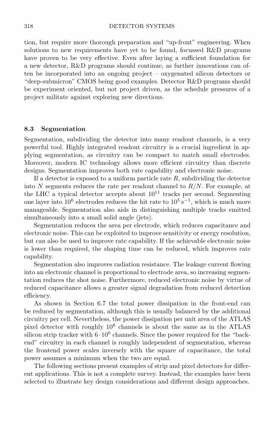
318 DETECTOR SYSTEMS
tion, but require more thorough preparation and “up-front” engineering. Whensolutions to new requirements have yet to be found, focussed R&D programshave proven to be very effective. Even after laying a sufficient foundation fora new detector, R&D programs should continue, as further innovations can of-ten be incorporated into an ongoing project – oxygenated silicon detectors or“deep-submicron” CMOS being good examples. Detector R&D programs shouldbe experiment oriented, but not project driven, as the schedule pressures of aproject militate against exploring new directions.
8.3 Segmentation
Segmentation, subdividing the detector into many readout channels, is a verypowerful tool. Highly integrated readout circuitry is a crucial ingredient in ap-plying segmentation, as circuitry can be compact to match small electrodes.Moreover, modern IC technology allows more efficient circuitry than discretedesigns. Segmentation improves both rate capability and electronic noise.
If a detector is exposed to a uniform particle rate R, subdividing the detectorinto N segments reduces the rate per readout channel to R/N . For example, atthe LHC a typical detector accepts about 1011 tracks per second. Segmentingone layer into 106 electrodes reduces the hit rate to 105 s−1, which is much moremanageable. Segmentation also aids in distinguishing multiple tracks emittedsimultaneously into a small solid angle (jets).
Segmentation reduces the area per electrode, which reduces capacitance andelectronic noise. This can be exploited to improve sensitivity or energy resolution,but can also be used to improve rate capability. If the achievable electronic noiseis lower than required, the shaping time can be reduced, which improves ratecapability.
Segmentation also improves radiation resistance. The leakage current flowinginto an electronic channel is proportional to electrode area, so increasing segmen-tation reduces the shot noise. Furthermore, reduced electronic noise by virtue ofreduced capacitance allows a greater signal degradation from reduced detectionefficiency.
As shown in Section 6.7 the total power dissipation in the front-end canbe reduced by segmentation, although this is usually balanced by the additionalcircuitry per cell. Nevertheless, the power dissipation per unit area of the ATLASpixel detector with roughly 108 channels is about the same as in the ATLASsilicon strip tracker with 6 ·106 channels. Since the power required for the “back-end” circuitry in each channel is roughly independent of segmentation, whereasthe frontend power scales inversely with the square of capacitance, the totalpower assumes a minimum when the two are equal.
The following sections present examples of strip and pixel detectors for differ-ent applications. This is not a complete survey. Instead, the examples have beenselected to illustrate key design considerations and different design approaches.
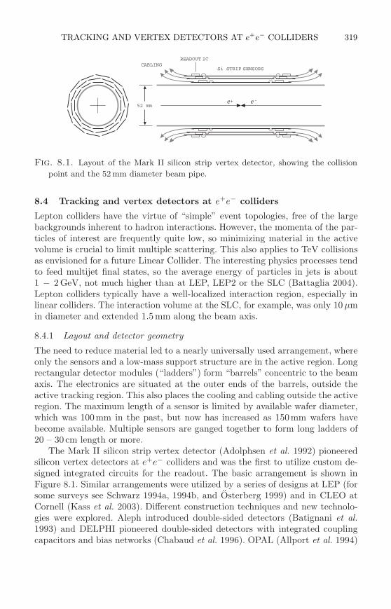
TRACKING AND VERTEX DETECTORS AT e+e− COLLIDERS 319
52 mm
CABLINGREADOUT IC
Si STRIP SENSORS
e e+ -
Fig. 8.1. Layout of the Mark II silicon strip vertex detector, showing the collision
point and the 52 mm diameter beam pipe.
8.4 Tracking and vertex detectors at e+e− colliders
Lepton colliders have the virtue of “simple” event topologies, free of the largebackgrounds inherent to hadron interactions. However, the momenta of the par-ticles of interest are frequently quite low, so minimizing material in the activevolume is crucial to limit multiple scattering. This also applies to TeV collisionsas envisioned for a future Linear Collider. The interesting physics processes tendto feed multijet final states, so the average energy of particles in jets is about1 − 2 GeV, not much higher than at LEP, LEP2 or the SLC (Battaglia 2004).Lepton colliders typically have a well-localized interaction region, especially inlinear colliders. The interaction volume at the SLC, for example, was only 10 µmin diameter and extended 1.5mm along the beam axis.
8.4.1 Layout and detector geometry
The need to reduce material led to a nearly universally used arrangement, whereonly the sensors and a low-mass support structure are in the active region. Longrectangular detector modules (“ladders”) form “barrels” concentric to the beamaxis. The electronics are situated at the outer ends of the barrels, outside theactive tracking region. This also places the cooling and cabling outside the activeregion. The maximum length of a sensor is limited by available wafer diameter,which was 100mm in the past, but now has increased as 150mm wafers havebecome available. Multiple sensors are ganged together to form long ladders of20 – 30 cm length or more.
The Mark II silicon strip vertex detector (Adolphsen et al. 1992) pioneeredsilicon vertex detectors at e+e− colliders and was the first to utilize custom de-signed integrated circuits for the readout. The basic arrangement is shown inFigure 8.1. Similar arrangements were utilized by a series of designs at LEP (forsome surveys see Schwarz 1994a, 1994b, and Osterberg 1999) and in CLEO atCornell (Kass et al. 2003). Different construction techniques and new technolo-gies were explored. Aleph introduced double-sided detectors (Batignani et al.1993) and DELPHI pioneered double-sided detectors with integrated couplingcapacitors and bias networks (Chabaud et al. 1996). OPAL (Allport et al. 1994)
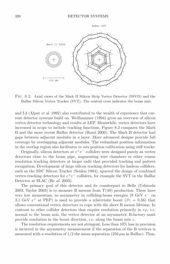
320 DETECTOR SYSTEMS
100 mm
Mark II SSVD
BaBar SVT
Fig. 8.2. Axial views of the Mark II Silicon Strip Vertex Detector (SSVD) and the
BaBar Silicon Vertex Tracker (SVT). The central cross indicates the beam axis.
and L3 (Alpat et al. 1992) also contributed to the wealth of experience that cur-rent detector systems build on. Weilhammer (1994) gives an overview of siliconvertex detector technology and results at LEP. Meanwhile, vertex detectors haveincreased in scope to include tracking functions. Figure 8.2 compares the MarkII and the more recent BaBar detector (Bozzi 2000). The Mark II detector hadgaps between adjacent modules in a layer. More advanced designs provide fullcoverage by overlapping adjacent modules. The redundant position informationin the overlap region also facilitates in situ position calibration using stiff tracks.
Originally, silicon detectors at e+e− colliders were designed purely as vertexdetectors close to the beam pipe, augmenting wire chambers or other coarseresolution tracking detectors at larger radii that provided tracking and patternrecognition. Development of large silicon tracking detectors for hadron colliders,such as the SDC Silicon Tracker (Seiden 1994), spurred the design of combinedvertex-tracking detectors for e+e− colliders, for example the SVT in the BaBarDetector at SLAC (Re al. 2003).
The primary goal of this detector and its counterpart in Belle (Ushiroda2003, Taylor 2003) is to measure B mesons from Υ(4S) production. These havevery low momentum, so asymmetry in colliding-beam energies (9 GeV e− on3.1 GeV e+ at PEP) is used to provide a relativistic boost (βγ = 0.56) thatallows conventional vertex detectors to cope with the short B meson lifetime. Incontrast to other collider detectors that require resolution primarily in rϕ, i.e.normal to the beam axis, the vertex detector at an asymmetric B-factory mustprovide resolution in the boost direction, i.e. along the beam axis z.
The resolution requirements are not stringent. Less than 10% loss in precisionis incurred in the asymmetry measurement if the separation of the B vertices ismeasured with a resolution of 1/2 the mean separation (250 µm in BaBar). Thus,
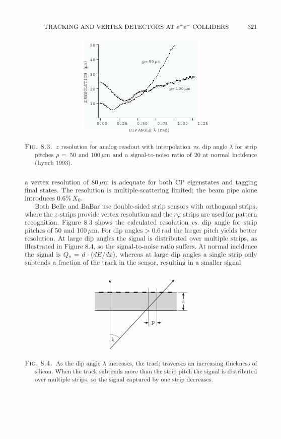
TRACKING AND VERTEX DETECTORS AT e+e− COLLIDERS 321
p= 50 m
p= 100 m
10
20
30
40
50
0.00 0.25 0.50 0.75 1.00 1.25
DIP ANGLE (rad)
zRESOLUTION
(m)
Fig. 8.3. z resolution for analog readout with interpolation vs. dip angle λ for strip
pitches p = 50 and 100 µm and a signal-to-noise ratio of 20 at normal incidence
(Lynch 1993).
a vertex resolution of 80 µm is adequate for both CP eigenstates and taggingfinal states. The resolution is multiple-scattering limited; the beam pipe aloneintroduces 0.6% X0.
Both Belle and BaBar use double-sided strip sensors with orthogonal strips,where the z-strips provide vertex resolution and the rϕ strips are used for patternrecognition. Figure 8.3 shows the calculated resolution vs. dip angle for strippitches of 50 and 100 µm. For dip angles > 0.6 rad the larger pitch yields betterresolution. At large dip angles the signal is distributed over multiple strips, asillustrated in Figure 8.4, so the signal-to-noise ratio suffers. At normal incidencethe signal is Qs = d · (dE/dx), whereas at large dip angles a single strip onlysubtends a fraction of the track in the sensor, resulting in a smaller signal
p
d
Fig. 8.4. As the dip angle λ increases, the track traverses an increasing thickness of
silicon. When the track subtends more than the strip pitch the signal is distributed
over multiple strips, so the signal captured by one strip decreases.
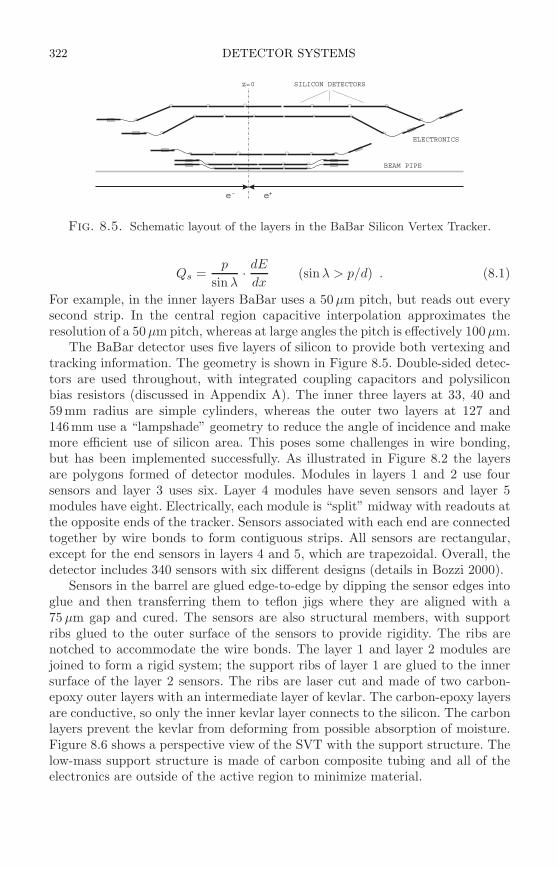
322 DETECTOR SYSTEMS
z=0
BEAM PIPE
e e- +
ELECTRONICS
SILICON DETECTORS
Fig. 8.5. Schematic layout of the layers in the BaBar Silicon Vertex Tracker.
Qs =p
sin λ· dE
dx(sinλ > p/d) . (8.1)
For example, in the inner layers BaBar uses a 50µm pitch, but reads out everysecond strip. In the central region capacitive interpolation approximates theresolution of a 50 µm pitch, whereas at large angles the pitch is effectively 100µm.
The BaBar detector uses five layers of silicon to provide both vertexing andtracking information. The geometry is shown in Figure 8.5. Double-sided detec-tors are used throughout, with integrated coupling capacitors and polysiliconbias resistors (discussed in Appendix A). The inner three layers at 33, 40 and59mm radius are simple cylinders, whereas the outer two layers at 127 and146mm use a “lampshade” geometry to reduce the angle of incidence and makemore efficient use of silicon area. This poses some challenges in wire bonding,but has been implemented successfully. As illustrated in Figure 8.2 the layersare polygons formed of detector modules. Modules in layers 1 and 2 use foursensors and layer 3 uses six. Layer 4 modules have seven sensors and layer 5modules have eight. Electrically, each module is “split” midway with readouts atthe opposite ends of the tracker. Sensors associated with each end are connectedtogether by wire bonds to form contiguous strips. All sensors are rectangular,except for the end sensors in layers 4 and 5, which are trapezoidal. Overall, thedetector includes 340 sensors with six different designs (details in Bozzi 2000).
Sensors in the barrel are glued edge-to-edge by dipping the sensor edges intoglue and then transferring them to teflon jigs where they are aligned with a75 µm gap and cured. The sensors are also structural members, with supportribs glued to the outer surface of the sensors to provide rigidity. The ribs arenotched to accommodate the wire bonds. The layer 1 and layer 2 modules arejoined to form a rigid system; the support ribs of layer 1 are glued to the innersurface of the layer 2 sensors. The ribs are laser cut and made of two carbon-epoxy outer layers with an intermediate layer of kevlar. The carbon-epoxy layersare conductive, so only the inner kevlar layer connects to the silicon. The carbonlayers prevent the kevlar from deforming from possible absorption of moisture.Figure 8.6 shows a perspective view of the SVT with the support structure. Thelow-mass support structure is made of carbon composite tubing and all of theelectronics are outside of the active region to minimize material.
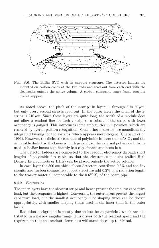
TRACKING AND VERTEX DETECTORS AT e+e− COLLIDERS 323
Fig. 8.6. The BaBar SVT with its support structure. The detector ladders are
mounted on carbon cones at the two ends and read out from each end with the
electronics outside the active volume. A carbon composite space frame provides
overall support.
As noted above, the pitch of the z-strips in layers 1 through 3 is 50 µm,but only every second strip is read out. In the outer layers the pitch of the z-strips is 210 µm. Since these layers are quite long, the width of a module doesnot allow a readout line for each z-strip, so a subset of the strips with loweroccupancy is ganged. This introduces some ambiguities in z position, which areresolved by overall pattern recognition. Some other detectors use monolithicallyintegrated bussing for the z-strips, which appears more elegant (Chabaud et al.1996). However, the dielectric constant of polyimide is lower then of SiO2 and theachievable dielectric thickness is much greater, so the external polyimide bussingused in BaBar incurs significantly less capacitance and costs less.
The detector ladders are connected to the readout electronics through shortlengths of polyimide flex cable, so that the electronics modules (called HighDensity Interconnects or HDIs) can be placed outside the active volume.
In each layer the 300 µm thick silicon detectors contribute 0.3% and the flexcircuits and carbon composite support structure add 0.2% of a radiation lengthto the tracker material, comparable to the 0.6% X0 of the beam pipe.
8.4.2 Electronics
The inner layers have the shortest strips and hence present the smallest capacitiveload, but the occupancy is highest. Conversely, the outer layers present the largestcapacitive load, but the smallest occupancy. The shaping times can be chosenappropriately, with smaller shaping times used in the inner than in the outerlayers.
Radiation background is mostly due to lost beam particles, which are dis-tributed in a narrow angular range. This drives both the readout speed and therequirement that the readout electronics withstand doses up to 3 Mrad.
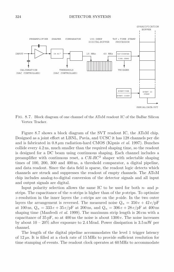
324 DETECTOR SYSTEMS
PREAMPLIFIER SHAPER COMPARATOR 193-DEEPDIGITAL BUFFER
ToT + TIME STAMPPROCESSOR
SPARSIFICATIONBUFFER
CR-RC 2
THRESHOLDCALIBRATION
INPUT ToT COUNTER
EVENT TIME
TIME STAMP
EVENT COUNT
TRIGGER
EVENT IDSTAMP
SERIAL DATA OUT
(DAC CONTROLLED) (DAC CONTROLLED)
15 MHz 60 MHz
Fig. 8.7. Block diagram of one channel of the AToM readout IC of the BaBar Silicon
Vertex Tracker.
Figure 8.7 shows a block diagram of the SVT readout IC, the AToM chip.Designed as a joint effort at LBNL, Pavia, and UCSC it has 128 channels per dieand is fabricated in 0.8µm radiation-hard CMOS (Kipnis et al. 1997). Bunchescollide every 4.2 ns, much smaller than the required shaping time, so the readoutis designed for a DC beam using continuous shaping. Each channel includes apreamplifier with continuous reset, a CR-RC2 shaper with selectable shapingtimes of 100, 200, 300 and 400ns, a threshold comparator, a digital pipeline,and data readout. Since the data field is sparse, the readout logic detects whichchannels are struck and suppresses the readout of empty channels. The AToMchip includes analog-to-digital conversion of the detector signals and all inputand output signals are digital.
Input polarity selection allows the same IC to be used for both n- and p-strips. The capacitance of the n-strips is higher than of the p-strips. To optimizez-resolution in the inner layers the z-strips are on the p-side. In the two outerlayers the arrangement is reversed. The measured noise Qn = 350 e + 42 e/pFat 100ns, Qn = 333 e + 35 e/pF at 200ns, and Qn = 306 e + 28 e/pF at 400nsshaping time (Manfredi et al. 1999). The maximum strip length is 26 cm with acapacitance of 35 pF, so at 400ns the noise is about 1300 e. The noise increasesby about 10 – 20% after exposure to 2.4Mrad. Power dissipation is 3.5mW perchannel.
The length of the digital pipeline accommodates the level 1 trigger latencyof 12 µs. It is filled at a clock rate of 15MHz to provide sufficient resolution fortime stamping of events. The readout clock operates at 60MHz to accommodate
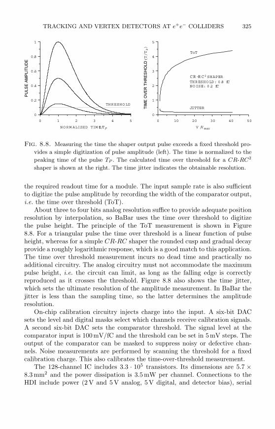
TRACKING AND VERTEX DETECTORS AT e+e− COLLIDERS 325
0 1 2 3 4 5
NO RM ALIZED TIM E t/TP
0
0.2
0.4
0.6
0.8
1
PULSEAMPLITUDE
THRESHO LD
0 10 20 30 40 50
V /Vmax
0
1
2
3
4
5
TIM
EOVER
THRESHOLD
(T/TP)
CR-RC 2 SHAPER
THRESHO LD: 0.8 fCNO ISE: 0.2 fC
ToT
JITTER
Fig. 8.8. Measuring the time the shaper output pulse exceeds a fixed threshold pro-
vides a simple digitization of pulse amplitude (left). The time is normalized to the
peaking time of the pulse TP . The calculated time over threshold for a CR-RC2
shaper is shown at the right. The time jitter indicates the obtainable resolution.
the required readout time for a module. The input sample rate is also sufficientto digitize the pulse amplitude by recording the width of the comparator output,i.e. the time over threshold (ToT).
About three to four bits analog resolution suffice to provide adequate positionresolution by interpolation, so BaBar uses the time over threshold to digitizethe pulse height. The principle of the ToT measurement is shown in Figure8.8. For a triangular pulse the time over threshold is a linear function of pulseheight, whereas for a simple CR-RC shaper the rounded cusp and gradual decayprovide a roughly logarithmic response, which is a good match to this application.The time over threshold measurement incurs no dead time and practically noadditional circuitry. The analog circuitry must not accommodate the maximumpulse height, i.e. the circuit can limit, as long as the falling edge is correctlyreproduced as it crosses the threshold. Figure 8.8 also shows the time jitter,which sets the ultimate resolution of the amplitude measurement. In BaBar thejitter is less than the sampling time, so the latter determines the amplituderesolution.
On-chip calibration circuitry injects charge into the input. A six-bit DACsets the level and digital masks select which channels receive calibration signals.A second six-bit DAC sets the comparator threshold. The signal level at thecomparator input is 100mV/fC and the threshold can be set in 5mV steps. Theoutput of the comparator can be masked to suppress noisy or defective chan-nels. Noise measurements are performed by scanning the threshold for a fixedcalibration charge. This also calibrates the time-over-threshold measurement.
The 128-channel IC includes 3.3 · 105 transistors. Its dimensions are 5.7 ×8.3 mm2 and the power dissipation is 3.5mW per channel. Connections to theHDI include power (2 V and 5 V analog, 5V digital, and detector bias), serial
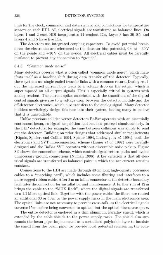
326 DETECTOR SYSTEMS
lines for the clock, command, and data signals, and connections for temperaturesensors on each HDI. All electrical signals are transferred as balanced lines. Onlayers 1 and 2 each HDI incorporates 14 readout ICs, Layer 3 has 20 ICs andlayers 4 and 5 have five ICs.
The detectors use integrated coupling capacitors. To avoid potential break-down the electronics are referenced to the detector bias potential, i.e. at −30Von the p-side and +30V on the n-side. All electrical cables must be carefullyinsulated to prevent any connection to “ground”.
8.4.3 “Common mode noise”
Many detectors observe what is often called “common mode noise”, which man-ifests itself as a baseline shift during data transfer off the detector. Typically,these systems use single-ended transfer links with a common return. During read-out the increased current flow leads to a voltage drop on the return, which issuperimposed on all output signals. This is especially critical in systems withanalog readout. The current spikes associated with the transitions of the digitalcontrol signals give rise to a voltage drop between the detector module and theoff-detector electronics, which also transfers to the analog signal. Many detectorbuilders unwittingly design this flaw into their system, leading many to believethat it is unavoidable.
Unlike previous collider vertex detectors BaBar operates with an essentiallycontinuous beam, so signal acquisition and readout proceed simultaneously. Inthe LEP detectors, for example, the time between collisions was ample to readout the detector. Building on prior designs that addressed similar requirements(Kipnis, Spieler, and Collins 1994, Spieler 1994, Ludewigt et al. 1994), both theelectronics and SVT interconnection scheme (Eisner et al. 1997) were carefullydesigned and the BaBar SVT operates without discernible noise pickup. Figure8.9 shows the connection scheme, which controls signal return paths and avoidsunnecessary ground connections (Nyman 1996). A key criterion is that all elec-trical signals are transferred as balanced pairs in which the net current remainsconstant.
Connections to the HDI are made through 40 cm long high-density polyimidecables to a “matching card”, which includes some filtering and interfaces to amore rugged ribbon cable. After 3m an inline connector at the detector boundaryfacilitates disconnection for installation and maintenance. A further run of 12mbrings the cable to the “MUX Rack”, where the digital signals are transferredto a 1.2Mb/s optical link. Together with the power cables the fibers are routedan additional 30 or 40m to the power supply racks in the main electronics area.The optical links are not necessary to prevent cross-talk, as the electrical signalstraverse 15m before being converted to optical, but the optical fibers save space.
The entire detector is enclosed in a thin aluminum Faraday shield, which isextended by the cable shields to the power supply racks. The shield also sur-rounds the beam pipe, implemented as a metallized polyimide layer to insulatethe shield from the beam pipe. To provide local potential referencing the com-
TRACKING AND VERTEX DETECTORS AT e+e− COLLIDERS 327
3m 40cm
12m
30m 40m
12m
3m40cm
TRACKERINLINECONNECT OR
INLINECONNECT OR
MA TCHINGCARD
MA TCHINGCARD
DATA DATA
PWR PWR
MUX RACK MUX RACK
POWER SUPPL Y RACKS
HDI HDI
TO DAQ TO DAQ
SAFETY GROUND
Fig. 8.9. Connection and cabling scheme of the BaBar SVT. (Adapted from Nyman
1996.)
mon connection of the power is capacitively coupled to the Faraday shield atthe matching card. Since all currents are balanced, the current flow between thetwo halves of the detector is negligible, so no noticeable potential drop buildsup between the two capacitively coupled reference connections in the matchingcards. A safety ground (connecting the Faraday shield to earth ground) is pro-vided through a separate cable, but this is independent of the signal transfer andhas no effect on the integrity of the signal transfer. It is there only for safety.Implementing a “clean” system is challenging, not because the necessary tech-niques are unknown, but because the prevailing “grounding mythology” must beresisted in every design meeting and every step of the way. “Grounding” and itspitfalls are discussed more in Chapter 9.
8.4.4 Noise limits in long strip detectors
The desire to reduce mass in the active region has driven designs towards layoutsthat place the electronics outside the active region. This has been a key consid-eration at B-factories, where the resolution is multiple scattering limited, butwill remain equally important at future linear colliders (Battaglia 2004). Herethe active region will be longer than in current e+e− detectors, so this raisesthe question of how long a strip detector could provide the required signal-to-noise ratio. Long strips increase the capacitive load C at the preamplifier input,contributing to the noise charge as
328 DETECTOR SYSTEMS
Q2n = i2nFiTs +
e2n
C2
Fv
Ts. (8.2)
The noise level can be maintained by reducing the input noise voltage spectraldensity en, the shaper noise coefficient Fv , or increasing the shaping time TS. Anincrease in shaping time TS is limited by occupancy and by the strip’s leakagecurrent, which both grow with strip length. As shown in Chapter 4 the shapernoise coefficients are approximately one, so large improvements will not obtainby utilizing sophisticated shapers. The equivalent input noise voltage is deter-mined by the input amplifier as discussed in Chapter 6 and by the thermal noiseassociated with the resistance of the strip electrodes, as noted in Chapter 3.Consider an FET input. As the strip capacitance increases the acceptable inputcapacitance of the amplifier increases, so its contribution to the equivalent inputnoise voltage decreases. Ultimately the thermal noise of the strip resistance willdominate. With increasing strip length the leakage current also increases, so itis useful to consider the noise when dominated by the sensor parameters leakagecurrent, capacitance, and strip resistance.
The leakage current of the sensor scales with the area subtended by an elec-trode
Ib = I0pld , (8.3)
where p is the strip pitch, l the length of an electrode and d the sensor thickness.I0 is the leakage current per unit volume. The corresponding shot noise current
i2ns = 2eIb ≡ 2elI ′b . (8.4)
Here and in the following primed quantities are normalized to the strip length.For a strip pitch of 50 µm a typical value is 1 nA per cm strip length, so for 50 cmlong strips the shot noise current is 130 fA/
√Hz.
The capacitance is the sum of the fringing capacitance and the capacitanceto the backplane. The fringing capacitance Css is a logarithmic function of theratio of strip width to pitch. Thus, we’ll neglect the dependence on strip widthand set the capacitance proportional to strip periphery 2(l+p). For strips p ≪ l,Css ≈ 2lC ′
ss. For typical designs the fringing capacitance is about 1 pF per cmstrip length, so for a 50 cm long detector the fringing capacitance is 50 pF. Thecapacitance to the backplane
Cb = εε0pl
d, (8.5)
so the total strip capacitance Cs = Css + Cb ≡ lC ′s. For a strip pitch of 50µm, a
strip length of 50 cm, and a detector thickness of 300µm the backplane capaci-tance is 8 pF, yielding a total strip capacitance of about 60pF.
Increasing the strip pitch will increase the leakage current per channel, buthave only a minor effect on the capacitance, until the strip pitch exceeds severalhundred microns. Thus, the sensor parameters that determine electronic noise
TRACKING AND VERTEX DETECTORS AT e+e− COLLIDERS 329
drive the design towards small strip pitches. The reduction in strip pitch is limitedby the width required by an electronic channel, which is about 50µm.
The strip resistance introduces a thermal noise voltage e2nR = 4kTR ≡
4kT lR′. The strip resistance R = ρwtl, where ρ is the resistivity of the electrodematerial, w the width of the electrode (not the pitch), and t is the electrodethickness. For sputtered aluminum the resistivity ρ ≈ 4 µΩ cm and a practicallimit to the deposition thickness is about 1µm. Thus, for a metallization widthof 20 µm the resistance is 20 Ω per cm length. For a 50 cm strip length the resis-tance is 1000 Ω with a thermal noise voltage of 4 nV/
√Hz. This places a lower
limit on the total noise voltage. At this voltage noise level both the voltage noiseand capacitance contributed by the input amplifier can be relatively small.
Thus, for a 50 cm strip length the sensor parameters that enter into theelectronic noise are Ib = 50 nA (ind = 130 fA/
√Hz), Cs = 60 pF, and enr =
4 nV/√
Hz, so the amplifier input noise is negligible. At the optimum shapingtime (equal current and voltage noise contributions)
TS =en
inC
√
Fv
Fi(8.6)
the equivalent noise charge
Q2n = 2eninC
√
FiFv . (8.7)
Since√
FiFv ≈√
Fi/Fv ≈ 1, we can determine the minimum noise due to sensorparameters alone,
Q2n ≈ 2enrindC = 2lC ′
√
(4kT lR′)(2qelI ′b) = 2l2C ′√
(4kTR′)(2qeI ′b) . (8.8)
If the shaping time is adjusted optimally as the strip length increases, the noisecharge increases proportionally to strip length. For the example parameters usedabove the noise due to the sensor alone is 1600 e at a shaping time of 2 µs.
If, on the other hand, the shaping time is scaled with strip length to maintainoccupancy
TS =T ′
S
l, (8.9)
the noise charge
Q2n = i2nTSFi +
e2nC2
TSFv ≈ i2n
T ′S
l+ e2
n
(lC ′)2
T ′S/l
= (2qelI′b)
T ′S
l+ (4kT lR′) l3
C ′2
T ′S
Q2n ≈ 2qeI
′bT
′S + (4kTR′) l4
C ′2
T ′S
(8.10)
increases with the square of the length.
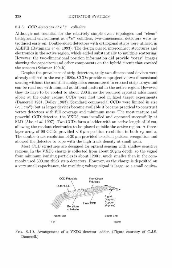
330 DETECTOR SYSTEMS
8.4.5 CCD detectors at e+e− colliders
Although not essential for the relatively simple event topologies and “clean”background environment at e+e− colliders, two-dimensional detectors were in-troduced early on. Double-sided detectors with orthogonal strips were utilized inALEPH (Batignani et al. 1993). The design placed interconnect structures andelectronics in the active region, which added substantially to multiple scattering.However, the two-dimensional position information did provide “x-ray” imagesshowing the capacitors and other components on the hybrid circuit that coveredthe sensors (Schwarz 1994b).
Despite the prevalence of strip detectors, truly two-dimensional devices werealready utilized in the early 1980s. CCDs provide nonprojective two-dimensionalsensing without the multihit ambiguities encountered in crossed-strip arrays andcan be read out with minimal additional material in the active region. However,they do have to be cooled to about 200K, so the required cryostat adds mass,albeit at the outer radius. CCDs were first used in fixed target experiments(Damerell 1981, Bailey 1983). Standard commercial CCDs were limited in size(< 1 cm2), but as larger devices became available it became practical to constructvertex detectors with full coverage and minimum mass. The most mature andpowerful CCD detector, the VXD3, was installed and operated successfully atSLD (Abe et al. 1997). Two CCDs form a ladder with an active length of 16 cm,allowing the readout electronics to be placed outside the active region. A three-layer array of 96 CCDs provided < 6 µm position resolution in both rϕ and z.The double track resolution of 20 µm provided excellent pattern recognition andallowed the detector to cope with the high track density at small radii.
Most CCD structures are designed for optical sensing with shallow sensitiveregions. In the VXD3 charge is collected from about 20 µm depth, so the signalfrom minimum ionizing particles is about 1200 e, much smaller than in the com-monly used 300 µm thick strip detectors. However, as the charge is deposited ona very small capacitance, the resulting voltage signal is large, so a small equiva-
4–97 8262A11
Outer CCD
Flex-CircuitFiducials
Pigtail(Kapton/Copperstripline)Beryllium
substrate
Inner CCD
South EndNorth End
CCD Fiducials
Fig. 8.10. Arrangement of a VXD3 detector ladder. (Figure courtesy of C.J.S.
Damerell.)
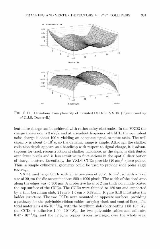
TRACKING AND VERTEX DETECTORS AT e+e− COLLIDERS 331
0.02
0
–0.02
–0.04
–0.06
5
0
–5–40
–200
South CCD
North CCD
All Dimensions in mm
8262A154–97
2040
0.06
0.04
0.02
0
–0.02
5
0
–5–40
–200
2040
Fig. 8.11. Deviations from planarity of mounted CCDs in VXD3. (Figure courtesy
of C.J.S. Damerell.)
lent noise charge can be achieved with rather noisy electronics. In the VXD3 thecharge conversion is 3 µV/e and at a readout frequency of 5 MHz the equivalentnoise charge is about 100 e, yielding an adequate signal-to-noise ratio. The wellcapacity is about 4 · 105 e, so the dynamic range is ample. Although the shallowcollection depth appears as a handicap with respect to signal charge, it is advan-tageous for track reconstruction at shallow incidence, as the signal is distributedover fewer pixels and is less sensitive to fluctuations in the spatial distributionof charge clusters. Essentially, the VXD3 CCDs provide (20µm)3 space points.Thus, a simple cylindrical geometry could be used to provide wide polar anglecoverage.
VXD3 used large CCDs with an active area of 80 × 16 mm2, so with a pixelsize of 20 µm the die accommodates 800×4000 pixels. The width of the dead areaalong the edges was < 300 µm. A protective layer of 2 µm thick polyimide coatedthe top surface of the CCDs. The CCDs were thinned to 180µm and supportedby a thin beryllium slab, 21 cm × 1.6 cm × 0.38 mm. Figure 8.10 illustrates theladder structure. The two CCDs were mounted on opposite surfaces, providinga pathway for the polyimide ribbon cables carrying clock and control lines. Thetotal material is 4.05·10−3X0, with the beryllium slab contributing 1.08·10−3X0,the CCDs + adhesive 1.60 · 10−3X0, the two polyimide cables and adhesive0.47 · 10−3X0, and the 17.8 µm copper traces, averaged over the whole area,
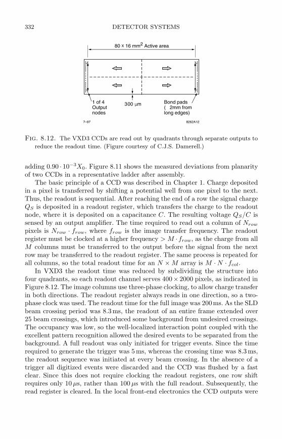
332 DETECTOR SYSTEMS
1 of 4Outputnodes
Bond pads( 2mm fromlong edges)
80 X 16 mm2 Active area
300 µm
7–97 8262A12
Fig. 8.12. The VXD3 CCDs are read out by quadrants through separate outputs to
reduce the readout time. (Figure courtesy of C.J.S. Damerell.)
adding 0.90 · 10−3X0. Figure 8.11 shows the measured deviations from planarityof two CCDs in a representative ladder after assembly.
The basic principle of a CCD was described in Chapter 1. Charge depositedin a pixel is transferred by shifting a potential well from one pixel to the next.Thus, the readout is sequential. After reaching the end of a row the signal chargeQS is deposited in a readout register, which transfers the charge to the readoutnode, where it is deposited on a capacitance C. The resulting voltage QS/C issensed by an output amplifier. The time required to read out a column of Nrow
pixels is Nrow · frow, where frow is the image transfer frequency. The readoutregister must be clocked at a higher frequency > M ·frow, as the charge from allM columns must be transferred to the output before the signal from the nextrow may be transferred to the readout register. The same process is repeated forall columns, so the total readout time for an N × M array is M · N · fcol.
In VXD3 the readout time was reduced by subdividing the structure intofour quadrants, so each readout channel serves 400× 2000 pixels, as indicated inFigure 8.12. The image columns use three-phase clocking, to allow charge transferin both directions. The readout register always reads in one direction, so a two-phase clock was used. The readout time for the full image was 200ms. As the SLDbeam crossing period was 8.3ms, the readout of an entire frame extended over25 beam crossings, which introduced some background from undesired crossings.The occupancy was low, so the well-localized interaction point coupled with theexcellent pattern recognition allowed the desired events to be separated from thebackground. A full readout was only initiated for trigger events. Since the timerequired to generate the trigger was 5 ms, whereas the crossing time was 8.3ms,the readout sequence was initiated at every beam crossing. In the absence of atrigger all digitized events were discarded and the CCD was flushed by a fastclear. Since this does not require clocking the readout registers, one row shiftrequires only 10 µs, rather than 100 µs with the full readout. Subsequently, theread register is cleared. In the local front-end electronics the CCD outputs were
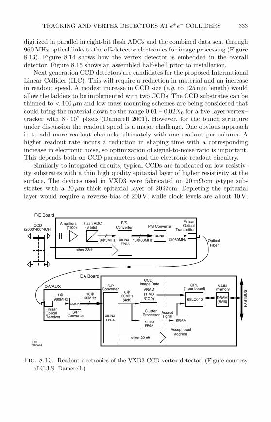
TRACKING AND VERTEX DETECTORS AT e+e− COLLIDERS 333
digitized in parallel in eight-bit flash ADCs and the combined data sent through960 MHz optical links to the off-detector electronics for image processing (Figure8.13). Figure 8.14 shows how the vertex detector is embedded in the overalldetector. Figure 8.15 shows an assembled half-shell prior to installation.
Next generation CCD detectors are candidates for the proposed InternationalLinear Collider (ILC). This will require a reduction in material and an increasein readout speed. A modest increase in CCD size (e.g. to 125mm length) wouldallow the ladders to be implemented with two CCDs. The CCD substrates can bethinned to < 100 µm and low-mass mounting schemes are being considered thatcould bring the material down to the range 0.01 – 0.02X0 for a five-layer vertex–tracker with 8 · 107 pixels (Damerell 2001). However, for the bunch structureunder discussion the readout speed is a major challenge. One obvious approachis to add more readout channels, ultimately with one readout per column. Ahigher readout rate incurs a reduction in shaping time with a correspondingincrease in electronic noise, so optimization of signal-to-noise ratio is important.This depends both on CCD parameters and the electronic readout circuitry.
Similarly to integrated circuits, typical CCDs are fabricated on low resistiv-ity substrates with a thin high quality epitaxial layer of higher resistivity at thesurface. The devices used in VXD3 were fabricated on 20 mΩ cm p-type sub-strates with a 20 µm thick epitaxial layer of 20 Ω cm. Depleting the epitaxiallayer would require a reverse bias of 200V, while clock levels are about 10V,
Optical Fiber
16@60MHz
CCD(2000*400*4CH)
Amplifiers(*100)
Flash ADC (8 bits)
8@5MHz 16@60MHz
P/SConverter
other 23ch
1@960MHz
FinisarOptical
Transmitter
F/E Board
P/S Converter
FinisarOpticalReceiver
1@960MHz
DA/AUX
S/PConverter
FA
ST
BU
S 8@20MHz(4ch)
other 20 ch
ClusterProcessor
VRAM(1 MB/CCD) 68LC040
CPU(1 per board)
MAINmemory
DRAM(8MB)
Acceptsignal
SRAM
CCDImage Data
DA Board
S/PConverter
XILINXFPGA
XILINX
FPGA
XILINX
FPGA
GLINK
GLINK
Accept pixeladdress
6–978262A24
Fig. 8.13. Readout electronics of the VXD3 CCD vertex detector. (Figure courtesy
of C.J.S. Damerell.)
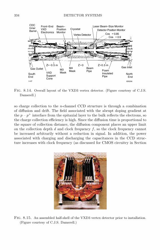
334 DETECTOR SYSTEMS
Front–EndVXDElectronics
Beam–PositionMonitor
CryostatLaser Beam–Size Monitor
Vertex Detector
Detector Position Monitor
Cos = 0.85
Cos = 0.9
4–97 8262A6
Gas InletZ=0.5 mZ=–0.5 m
Gas Outlet
CDCInnerBarrel
SouthEnd
NorthEnd
VXDSupportCone
Z = 0BeamPipe
M4Mask
M3Mask
FoamInsulatedPipe
Fig. 8.14. Overall layout of the VXD3 vertex detector. (Figure courtesy of C.J.S.
Damerell.)
so charge collection to the n-channel CCD structure is through a combinationof diffusion and drift. The field associated with the abrupt doping gradient atthe p – p+ interface from the epitaxial layer to the bulk reflects the electrons, sothe charge collection efficiency is high. Since the diffusion time is proportional tothe square of collection distance, the diffusion component places an upper limiton the collection depth d and clock frequency f , so the clock frequency cannotbe increased arbitrarily without a reduction in signal. In addition, the powerassociated with charging and discharging the capacitances in the CCD struc-ture increases with clock frequency (as discussed for CMOS circuitry in Section
Fig. 8.15. An assembled half-shell of the VXD3 vertex detector prior to installation.
(Figure courtesy of C.J.S. Damerell.)
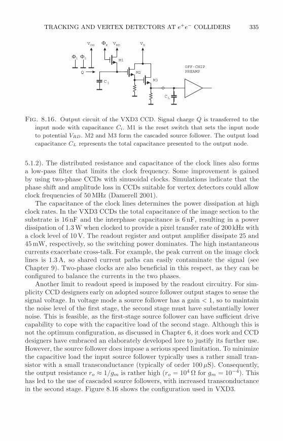
TRACKING AND VERTEX DETECTORS AT e+e− COLLIDERS 335
Q
1 2
V
C
C
V VOG
i
L
RDR D
OFF-CHIPPREAMP
M1
M3
M2
Fig. 8.16. Output circuit of the VXD3 CCD. Signal charge Q is transferred to the
input node with capacitance Ci. M1 is the reset switch that sets the input node
to potential VRD. M2 and M3 form the cascaded source follower. The output load
capacitance CL represents the total capacitance presented to the output node.
5.1.2). The distributed resistance and capacitance of the clock lines also formsa low-pass filter that limits the clock frequency. Some improvement is gainedby using two-phase CCDs with sinusoidal clocks. Simulations indicate that thephase shift and amplitude loss in CCDs suitable for vertex detectors could allowclock frequencies of 50MHz (Damerell 2001).
The capacitance of the clock lines determines the power dissipation at highclock rates. In the VXD3 CCDs the total capacitance of the image section to thesubstrate is 16 nF and the interphase capacitance is 6 nF, resulting in a powerdissipation of 1.3W when clocked to provide a pixel transfer rate of 200kHz witha clock level of 10V. The readout register and output amplifier dissipate 25 and45mW, respectively, so the switching power dominates. The high instantaneouscurrents exacerbate cross-talk. For example, the peak current on the image clocklines is 1.3A, so shared current paths can easily contaminate the signal (seeChapter 9). Two-phase clocks are also beneficial in this respect, as they can beconfigured to balance the currents in the two phases.
Another limit to readout speed is imposed by the readout circuitry. For sim-plicity CCD designers early on adopted source follower output stages to sense thesignal voltage. In voltage mode a source follower has a gain < 1, so to maintainthe noise level of the first stage, the second stage must have substantially lowernoise. This is feasible, as the first-stage source follower can have sufficient drivecapability to cope with the capacitive load of the second stage. Although this isnot the optimum configuration, as discussed in Chapter 6, it does work and CCDdesigners have embraced an elaborately developed lore to justify its further use.However, the source follower does impose a serious speed limitation. To minimizethe capacitive load the input source follower typically uses a rather small tran-sistor with a small transconductance (typically of order 100µS). Consequently,the output resistance ro ≈ 1/gm is rather high (ro = 104 Ω for gm = 10−4). Thishas led to the use of cascaded source followers, with increased transconductancein the second stage. Figure 8.16 shows the configuration used in VXD3.
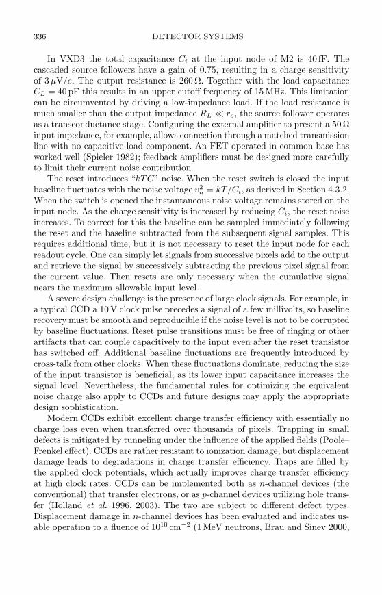
336 DETECTOR SYSTEMS
In VXD3 the total capacitance Ci at the input node of M2 is 40 fF. Thecascaded source followers have a gain of 0.75, resulting in a charge sensitivityof 3 µV/e. The output resistance is 260 Ω. Together with the load capacitanceCL = 40 pF this results in an upper cutoff frequency of 15 MHz. This limitationcan be circumvented by driving a low-impedance load. If the load resistance ismuch smaller than the output impedance RL ≪ ro, the source follower operatesas a transconductance stage. Configuring the external amplifier to present a 50 Ωinput impedance, for example, allows connection through a matched transmissionline with no capacitive load component. An FET operated in common base hasworked well (Spieler 1982); feedback amplifiers must be designed more carefullyto limit their current noise contribution.
The reset introduces “kTC” noise. When the reset switch is closed the inputbaseline fluctuates with the noise voltage v2
n = kT/Ci, as derived in Section 4.3.2.When the switch is opened the instantaneous noise voltage remains stored on theinput node. As the charge sensitivity is increased by reducing Ci, the reset noiseincreases. To correct for this the baseline can be sampled immediately followingthe reset and the baseline subtracted from the subsequent signal samples. Thisrequires additional time, but it is not necessary to reset the input node for eachreadout cycle. One can simply let signals from successive pixels add to the outputand retrieve the signal by successively subtracting the previous pixel signal fromthe current value. Then resets are only necessary when the cumulative signalnears the maximum allowable input level.
A severe design challenge is the presence of large clock signals. For example, ina typical CCD a 10V clock pulse precedes a signal of a few millivolts, so baselinerecovery must be smooth and reproducible if the noise level is not to be corruptedby baseline fluctuations. Reset pulse transitions must be free of ringing or otherartifacts that can couple capacitively to the input even after the reset transistorhas switched off. Additional baseline fluctuations are frequently introduced bycross-talk from other clocks. When these fluctuations dominate, reducing the sizeof the input transistor is beneficial, as its lower input capacitance increases thesignal level. Nevertheless, the fundamental rules for optimizing the equivalentnoise charge also apply to CCDs and future designs may apply the appropriatedesign sophistication.
Modern CCDs exhibit excellent charge transfer efficiency with essentially nocharge loss even when transferred over thousands of pixels. Trapping in smalldefects is mitigated by tunneling under the influence of the applied fields (Poole–Frenkel effect). CCDs are rather resistant to ionization damage, but displacementdamage leads to degradations in charge transfer efficiency. Traps are filled bythe applied clock potentials, which actually improves charge transfer efficiencyat high clock rates. CCDs can be implemented both as n-channel devices (theconventional) that transfer electrons, or as p-channel devices utilizing hole trans-fer (Holland et al. 1996, 2003). The two are subject to different defect types.Displacement damage in n-channel devices has been evaluated and indicates us-able operation to a fluence of 1010 cm−2 (1 MeV neutrons, Brau and Sinev 2000,
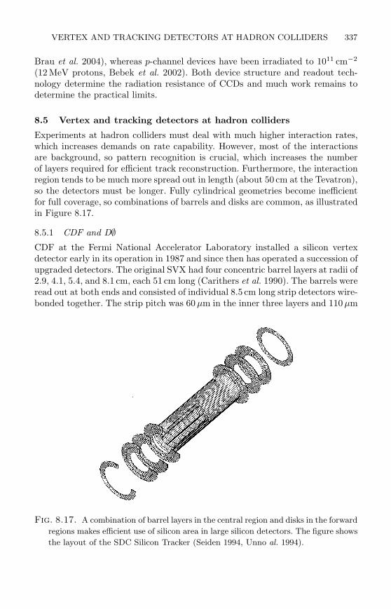
VERTEX AND TRACKING DETECTORS AT HADRON COLLIDERS 337
Brau et al. 2004), whereas p-channel devices have been irradiated to 1011 cm−2
(12 MeV protons, Bebek et al. 2002). Both device structure and readout tech-nology determine the radiation resistance of CCDs and much work remains todetermine the practical limits.
8.5 Vertex and tracking detectors at hadron colliders
Experiments at hadron colliders must deal with much higher interaction rates,which increases demands on rate capability. However, most of the interactionsare background, so pattern recognition is crucial, which increases the numberof layers required for efficient track reconstruction. Furthermore, the interactionregion tends to be much more spread out in length (about 50 cm at the Tevatron),so the detectors must be longer. Fully cylindrical geometries become inefficientfor full coverage, so combinations of barrels and disks are common, as illustratedin Figure 8.17.
8.5.1 CDF and D∅CDF at the Fermi National Accelerator Laboratory installed a silicon vertexdetector early in its operation in 1987 and since then has operated a succession ofupgraded detectors. The original SVX had four concentric barrel layers at radii of2.9, 4.1, 5.4, and 8.1 cm, each 51 cm long (Carithers et al. 1990). The barrels wereread out at both ends and consisted of individual 8.5 cm long strip detectors wire-bonded together. The strip pitch was 60 µm in the inner three layers and 110 µm
Fig. 8.17. A combination of barrel layers in the central region and disks in the forward
regions makes efficient use of silicon area in large silicon detectors. The figure shows
the layout of the SDC Silicon Tracker (Seiden 1994, Unno al. 1994).
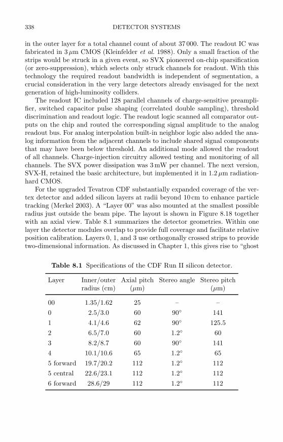
338 DETECTOR SYSTEMS
in the outer layer for a total channel count of about 37 000. The readout IC wasfabricated in 3 µm CMOS (Kleinfelder et al. 1988). Only a small fraction of thestrips would be struck in a given event, so SVX pioneered on-chip sparsification(or zero-suppression), which selects only struck channels for readout. With thistechnology the required readout bandwidth is independent of segmentation, acrucial consideration in the very large detectors already envisaged for the nextgeneration of high-luminosity colliders.
The readout IC included 128 parallel channels of charge-sensitive preampli-fier, switched capacitor pulse shaping (correlated double sampling), thresholddiscrimination and readout logic. The readout logic scanned all comparator out-puts on the chip and routed the corresponding signal amplitude to the analogreadout bus. For analog interpolation built-in neighbor logic also added the ana-log information from the adjacent channels to include shared signal componentsthat may have been below threshold. An additional mode allowed the readoutof all channels. Charge-injection circuitry allowed testing and monitoring of allchannels. The SVX power dissipation was 3mW per channel. The next version,SVX-H, retained the basic architecture, but implemented it in 1.2 µm radiation-hard CMOS.
For the upgraded Tevatron CDF substantially expanded coverage of the ver-tex detector and added silicon layers at radii beyond 10 cm to enhance particletracking (Merkel 2003). A “Layer 00” was also mounted at the smallest possibleradius just outside the beam pipe. The layout is shown in Figure 8.18 togetherwith an axial view. Table 8.1 summarizes the detector geometries. Within onelayer the detector modules overlap to provide full coverage and facilitate relativeposition calibration. Layers 0, 1, and 3 use orthogonally crossed strips to providetwo-dimensional information. As discussed in Chapter 1, this gives rise to “ghost
Table 8.1 Specifications of the CDF Run II silicon detector.
Layer Inner/outer Axial pitch Stereo angle Stereo pitchradius (cm) (µm) (µm)
00 1.35/1.62 25 – –
0 2.5/3.0 60 90 141
1 4.1/4.6 62 90 125.5
2 6.5/7.0 60 1.2 60
3 8.2/8.7 60 90 141
4 10.1/10.6 65 1.2 65
5 forward 19.7/20.2 112 1.2 112
5 central 22.6/23.1 112 1.2 112
6 forward 28.6/29 112 1.2 112
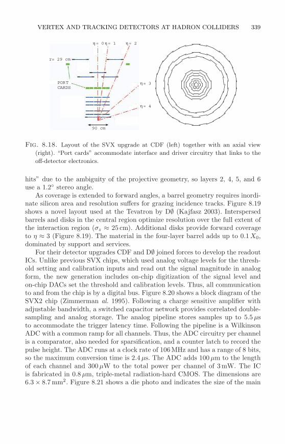
VERTEX AND TRACKING DETECTORS AT HADRON COLLIDERS 339
= 0= 1 = 2
= 3
= 4
90 cm
r= 29 cm
PORTCARDS
Fig. 8.18. Layout of the SVX upgrade at CDF (left) together with an axial view
(right). “Port cards” accommodate interface and driver circuitry that links to the
off-detector electronics.
hits” due to the ambiguity of the projective geometry, so layers 2, 4, 5, and 6use a 1.2 stereo angle.
As coverage is extended to forward angles, a barrel geometry requires inordi-nate silicon area and resolution suffers for grazing incidence tracks. Figure 8.19shows a novel layout used at the Tevatron by D∅ (Kajfasz 2003). Interspersedbarrels and disks in the central region optimize resolution over the full extent ofthe interaction region (σz ≈ 25 cm). Additional disks provide forward coverageto η ≈ 3 (Figure 8.19). The material in the four-layer barrel adds up to 0.1 X0,dominated by support and services.
For their detector upgrades CDF and D∅ joined forces to develop the readoutICs. Unlike previous SVX chips, which used analog voltage levels for the thresh-old setting and calibration inputs and read out the signal magnitude in analogform, the new generation includes on-chip digitization of the signal level andon-chip DACs set the threshold and calibration levels. Thus, all communicationto and from the chip is by a digital bus. Figure 8.20 shows a block diagram of theSVX2 chip (Zimmerman al. 1995). Following a charge sensitive amplifier withadjustable bandwidth, a switched capacitor network provides correlated double-sampling and analog storage. The analog pipeline stores samples up to 5.5 µsto accommodate the trigger latency time. Following the pipeline is a WilkinsonADC with a common ramp for all channels. Thus, the ADC circuitry per channelis a comparator, also needed for sparsification, and a counter latch to record thepulse height. The ADC runs at a clock rate of 106MHz and has a range of 8 bits,so the maximum conversion time is 2.4 µs. The ADC adds 100 µm to the lengthof each channel and 300 µW to the total power per channel of 3mW. The ICis fabricated in 0.8 µm, triple-metal radiation-hard CMOS. The dimensions are6.3 × 8.7 mm2. Figure 8.21 shows a die photo and indicates the size of the main
340 DETECTOR SYSTEMS
Fig. 8.19. D∅ uses interspersed disks and barrels in the central region, with additional
disks to provide forward coverage. The D∅ barrel is 762 mm long with four layers
distributed over 2.7 to 9.4 cm radius. The outer disks have 26 cm radius and the
overall length is 2.5 m. The detector has about 8 · 105 readout channels and 3 m2 of
silicon area (Bean 2001). (Figure courtesy of A. Bean.)
circuit blocks. The 128 signal channels are laid out on a 42µm pitch to providespace at the edges of the chip for bussing and common logic.
Despite what its name implies, the analog pipeline does not shift signals se-quentially. Instead the signal is stored in one of the memory locations B1 – B32and remains there until retrieved. Opening or closing a switch injects chargethrough the gate–channel capacitance, introducing a baseline shift, which is re-moved by correlated double sampling. Prior to signal acquisition the baselinevoltage VBL is sampled and stored in the pipeline. When a subsequent signalVS is read, the level applied to the comparator is the sum of the signal and thebaseline VS +VBL. When switches SC and SCR are closed, the voltage VS +VBL
is impressed on the coupling capacitor CC , as closing SCR establishes a lowimpedance at the comparator input through shunt feedback. To subtract thebaseline, the baseline sample stored in the pipeline is selected, while openingswitch SCR. This sets the voltage at the left side of CC to VBL, while the volt-age across CC is still VS + VBL, so the two sample voltages in series yield VS
at the comparator input. Although implemented differently, this performs thesame function as discussed in Section 4.5. The circuit utilizes switched capacitorcircuitry for many functions. The operating modes and switching sequences aredescribed in the SVX2 manual (Yarema et al. 1994).
The circuit can accept both positive and negative polarity input signals. Thepreamplifier is designed with sufficient bipolar dynamic range. Switching polarityinvolves shifting the baseline of the analog pipeline to increase the range for either
VERTEX AND TRACKING DETECTORS AT HADRON COLLIDERS 341
PREAMPLIFIER DATASPARSIFICATION
CALIBRATION
INPUT
DATA OUT
(DAC CONTROLLED)
PREAMP RESET
BANDWIDTHCONTROL
PIPELINE RESETCOMPARATOR
RESET
B1
B2
B3
B32
COMPARATORTHRESHOLD(DAC CONTROLLED)
COMP ARATORRESET
COMMONRAMP
GENERATOR
COMPARATORLATCH &
NEIGHBOR LOGIC
ANALOG PIPELINE
S C SC C CR
Fig. 8.20. Block diagram of the SVX2 chip. For details of the operating modes and
switching sequences see Yarema et al. (1994).
positive or negative excursions. In addition, the polarity of the ADC ramp andcomparator are reversed.
The neighbor logic allows three modes: read only channels whose level ex-ceeded threshold, read “struck” channels and their two neighbors, and read allchannels. The hit threshold is set digitally and is common to all channels on achip. This setting is rather coarse (about 2000 e), but external adjustment of theADC ramp start voltage provides a threshold resolution of about 400 e.
The SVX2 IC (used by D∅) is designed for sequential signal acquisition andreadout. A further development, SVX3 (used by CDF) allows concurrent read-write, so that signal acquisition and readout can proceed concurrently (Garcia-Sciveres et al. 1999). The floor plan is similar to SVX2, but the die size increasedto 6.26× 12 mm2. The measured noise Qn ≈ 2400 e at an input load of 33 pF, apreamplifier rise time of 60ns, and a sample time of 120ns. In the SVX detectordesign the concurrent readout introduces substantial common mode noise. Acompensation scheme was implemented on-chip that uses all channels in a chipto calculate a common pedestal event by event and subtract it during digitization.A subsequent version implemented in 0.25 µm CMOS, the SVX4, was designedand tested for planned upgrades of CDF and D∅ (Krieger et al. 2004). At the106MHz digitizer speed and 53MHz readout rate the SVX4 achieves 2000 e noisewith a 40pF input load, while dissipating 2mW/channel at 2.5V supply voltage.The IC was tested to > 20 Mrad total dose.
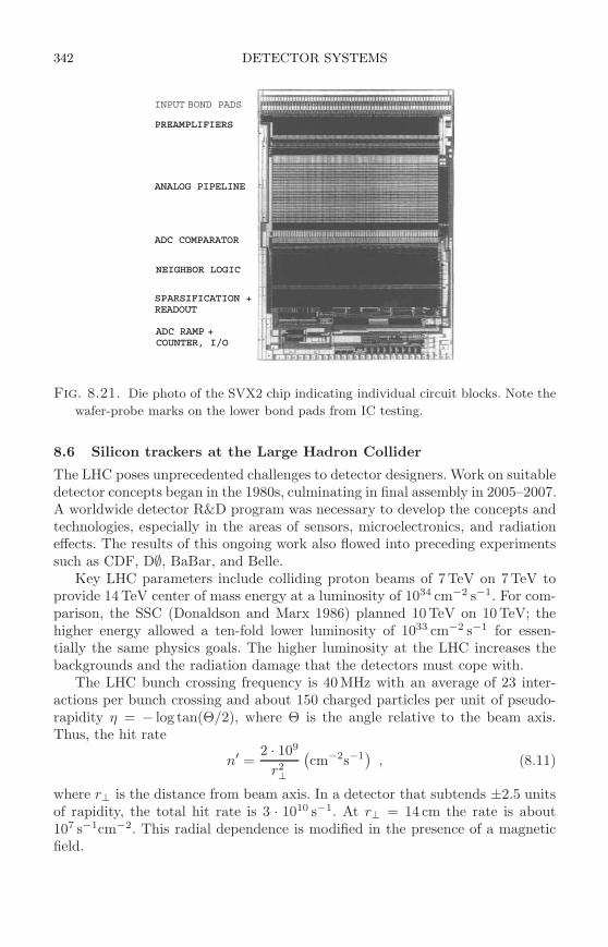
342 DETECTOR SYSTEMS
ADC COMPARATOR
INPUT BOND PADS
PREAMPLIFIERS
ANALOG PIPELINE
NEIGHBOR LOGIC
SPARSIFICATION +READOUT
ADC RAMP +COUNTER, I/O
ADC COMPARATOR
PREAMPLIFIERS
ANALOG PIPELINE
NEIGHBOR LOGIC
SPARSIFICATION +READOUT
ADC RAMP +COUNTER, I/O
Fig. 8.21. Die photo of the SVX2 chip indicating individual circuit blocks. Note the
wafer-probe marks on the lower bond pads from IC testing.
8.6 Silicon trackers at the Large Hadron Collider
The LHC poses unprecedented challenges to detector designers. Work on suitabledetector concepts began in the 1980s, culminating in final assembly in 2005–2007.A worldwide detector R&D program was necessary to develop the concepts andtechnologies, especially in the areas of sensors, microelectronics, and radiationeffects. The results of this ongoing work also flowed into preceding experimentssuch as CDF, D∅, BaBar, and Belle.
Key LHC parameters include colliding proton beams of 7TeV on 7TeV toprovide 14TeV center of mass energy at a luminosity of 1034 cm−2 s−1. For com-parison, the SSC (Donaldson and Marx 1986) planned 10TeV on 10TeV; thehigher energy allowed a ten-fold lower luminosity of 1033 cm−2 s−1 for essen-tially the same physics goals. The higher luminosity at the LHC increases thebackgrounds and the radiation damage that the detectors must cope with.
The LHC bunch crossing frequency is 40MHz with an average of 23 inter-actions per bunch crossing and about 150 charged particles per unit of pseudo-rapidity η = − log tan(Θ/2), where Θ is the angle relative to the beam axis.Thus, the hit rate
n′ =2 · 109
r2⊥
(
cm−2s−1)
, (8.11)
where r⊥ is the distance from beam axis. In a detector that subtends ±2.5 unitsof rapidity, the total hit rate is 3 · 1010 s−1. At r⊥ = 14 cm the rate is about107 s−1cm−2. This radial dependence is modified in the presence of a magneticfield.
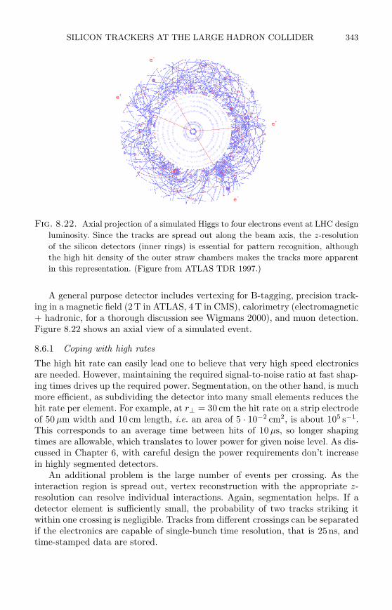
SILICON TRACKERS AT THE LARGE HADRON COLLIDER 343
e+
e-
e+
e-
Fig. 8.22. Axial projection of a simulated Higgs to four electrons event at LHC design
luminosity. Since the tracks are spread out along the beam axis, the z-resolution
of the silicon detectors (inner rings) is essential for pattern recognition, although
the high hit density of the outer straw chambers makes the tracks more apparent
in this representation. (Figure from ATLAS TDR 1997.)
A general purpose detector includes vertexing for B-tagging, precision track-ing in a magnetic field (2T in ATLAS, 4 T in CMS), calorimetry (electromagnetic+ hadronic, for a thorough discussion see Wigmans 2000), and muon detection.Figure 8.22 shows an axial view of a simulated event.
8.6.1 Coping with high rates
The high hit rate can easily lead one to believe that very high speed electronicsare needed. However, maintaining the required signal-to-noise ratio at fast shap-ing times drives up the required power. Segmentation, on the other hand, is muchmore efficient, as subdividing the detector into many small elements reduces thehit rate per element. For example, at r⊥ = 30 cm the hit rate on a strip electrodeof 50 µm width and 10 cm length, i.e. an area of 5 · 10−2 cm2, is about 105 s−1.This corresponds to an average time between hits of 10 µs, so longer shapingtimes are allowable, which translates to lower power for given noise level. As dis-cussed in Chapter 6, with careful design the power requirements don’t increasein highly segmented detectors.
An additional problem is the large number of events per crossing. As theinteraction region is spread out, vertex reconstruction with the appropriate z-resolution can resolve individual interactions. Again, segmentation helps. If adetector element is sufficiently small, the probability of two tracks striking itwithin one crossing is negligible. Tracks from different crossings can be separatedif the electronics are capable of single-bunch time resolution, that is 25ns, andtime-stamped data are stored.
344 DETECTOR SYSTEMS
Semiconductor detectors are well-matched to these requirements and they arekey components in all LHC experiments. Patterning the sensor at the “µm-scale”is straightforward and monolithically integrated electronics can be mounted lo-cally with on-chip multiplexing or sparsification to reduce the cable plant. Thefast collection times of semiconductor are very advantageous; achieving collectiontimes < 25ns with a 300 µm thick sensor is quite practical.
8.6.2 Radiation damage
The high rates bring another problem with them; radiation damage, both in thesensors and the electronics. There are two sources of particles, beam collisionsand neutron albedo from calorimeter. Estimated fluences per year at designluminosity expressed in equivalent 1 MeV neutrons are 5 ·1013 cm−2 at r = 10 cmand 2 · 1013 cm−2 at r = 30 cm. The corresponding ionizing doses are 30 kGy(3Mrad) at 10 cm and 4 kGy (400 krad) at 30 cm. In reality, complex maps arerequired of the radiation flux, which is dependent on local material distribution(examples in ATLAS TDR 1997).
As discussed in Chapter 7, displacement damage in the sensor leads to anincrease in leakage current
IR = I0 + αΦAd , (8.12)
which in the electronics increases the shot noise
Q2ni = 2eIdFiTS . (8.13)
The leakage current drops exponentially with temperature
IR(T ) ∝ T 2e−E/2kT , (8.14)
so even moderate reductions in temperature bring a significant improvement.The electronic shot noise can be reduced by choosing short shaping times.
Furthermore, reducing the area of a detector element reduces the leakage currentper channel, so the shot noise is also smaller. Again, segmentation is advanta-geous.
Reducing the leakage current by cooling is crucial for another reason. Thepower due to the leakage current together with the bias voltage leads to self-heating of the detector. Unless the sensor is cooled adequately, the increasedpower dissipation increases the temperature, which increases the bias currentexponentially and leads to thermal runaway (Kohriki et al. 1996).
The second effect of displacement damage is an increase in the required oper-ating voltage. Bias voltages can be maintained at reliable levels by thinning thesensor and by allowing for operation below full charge collection. This reducesthe signal and requires lower noise to maintain the required signal-to-noise ratio.Again, segmentation helps, as the decreased area of a detector element reducesthe capacitance and the achievable noise level.
SILICON TRACKERS AT THE LARGE HADRON COLLIDER 345
In the course of developing silicon detector systems many unexpected prob-lems arose and invariably solutions were found. Key is the use of a highly devel-oped technology, which provides performance reserves and design flexibility. Itis tempting to favor a new technology because it appears to offer a “silver bul-let” against one specific problem, but systems depend on the interplay of manydesign considerations. For this reason many “advanced” technologies have fallenby the wayside.
8.6.3 Layout
General purpose detectors provide full coverage by a combination of barrel anddisk layers. Both ATLAS (Turala al. 2001, Unno al. 2003) and CMS (Abbaneo2004) use barrels in the central region and disks in the forward regions to providethe required coverage and tracking performance with minimum silicon area. TheATLAS SemiConductor Tracker (SCT) has about 60 m2 of silicon with 6 · 106
strip detector channels, augmented by a gaseous outer tracking detector. Aftergoing rather far in the development of a mixed silicon-gaseous detector systemCMS decided to build an all-silicon tracker with about 230 m2 of silicon and 107
strip detector channels. Both ATLAS and CMS use pixel devices covering 1 –2 m2 with 50 – 100 million channels at the inner radii (< 15 cm) because of theirsuperior pattern recognition at high track densities and radiation resistance. Thesmall capacitance allows low noise Qn ≈ 200 e at sufficiently fast shaping times,so the system starts out with a very high signal-to-noise ratio. These performancereserves allow greater degradation of signal and noise with radiation damage thanin a silicon strip system, which extends the lifetime. Strips take over at largerradii to minimize material and cost.
In ATLAS four layers of silicon strips are used at radii of 30, 37, 44, and 51 cminside a superconducting solenoid with a 2T magnetic field (Figure 8.23). Beyond56 cm radius a 70-layer straw-tube gaseous tracking and transition radiationdetector (TRT) provides at least 40 hits per track. The TRT is operating closeto its limits at 1034 luminosity, but was retained for cost reasons. At both endsan array of 9 disks arranged at distances |z| = 0.85 m to 2.7m provide coverageat rapidity |η| > 1.2. Resolution in the barrel is determined by the strip pitchof 80 µm in rϕ and 40mrad small angle stereo in z. In the disks the strips goradially, with pitches ranging from 55 to 90 µm, using a 40mrad stereo anglefor r-resolution. All modules are double-sided, formed by gluing two single-sideddetectors back-to-back under an angle of 40mrad. Three layers of pixel detectorsat 5.1, 9.9, and 12.3 cm in the central region and three pixel disk layers at eachend provide the two track resolution and radiation resistance required close tothe interaction region. The pixels are 50µm × 400 µm, with the long dimensionalong the beam axis to accommodate inclined tracks. The pixel subsystem isenclosed within the pixel support tube and can be inserted or removed as a unitto facilitate replacement. Services are brought out to patch panels at the cryostatwall through the gaps between the TRT subunits, which leads to significant localincreases in the material distribution.
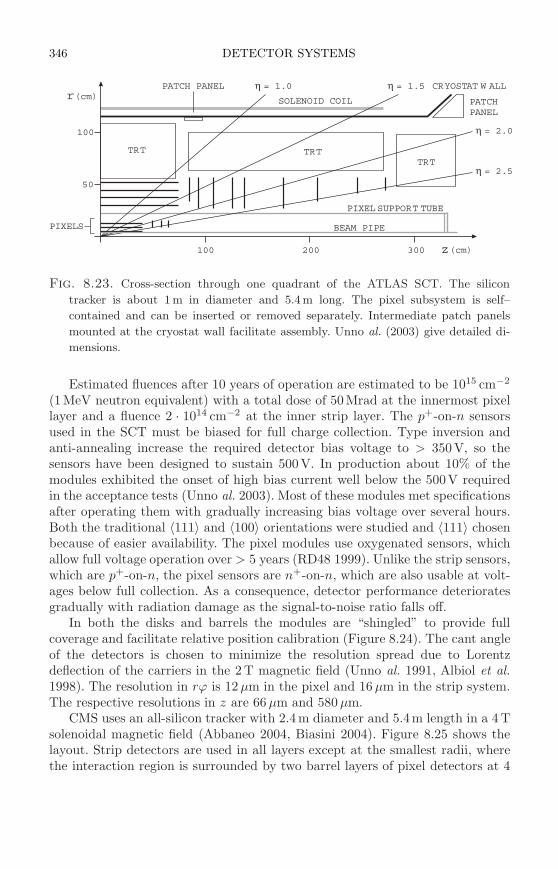
346 DETECTOR SYSTEMS
TRT TRTTRT
SOLENOID COIL
CRYOSTAT W ALLr(cm)
z(cm)
BEAM PIPE
PIXEL SUPPORT TUBE
PATCHPANEL
PATCH PANEL = 1.0 = 1.5
= 2.0
= 2.5
100
50
100 200 300
PIXELS
Fig. 8.23. Cross-section through one quadrant of the ATLAS SCT. The silicon
tracker is about 1 m in diameter and 5.4 m long. The pixel subsystem is self–
contained and can be inserted or removed separately. Intermediate patch panels
mounted at the cryostat wall facilitate assembly. Unno al. (2003) give detailed di-
mensions.
Estimated fluences after 10 years of operation are estimated to be 1015 cm−2
(1MeV neutron equivalent) with a total dose of 50Mrad at the innermost pixellayer and a fluence 2 · 1014 cm−2 at the inner strip layer. The p+-on-n sensorsused in the SCT must be biased for full charge collection. Type inversion andanti-annealing increase the required detector bias voltage to > 350V, so thesensors have been designed to sustain 500V. In production about 10% of themodules exhibited the onset of high bias current well below the 500V requiredin the acceptance tests (Unno al. 2003). Most of these modules met specificationsafter operating them with gradually increasing bias voltage over several hours.Both the traditional 〈111〉 and 〈100〉 orientations were studied and 〈111〉 chosenbecause of easier availability. The pixel modules use oxygenated sensors, whichallow full voltage operation over > 5 years (RD48 1999). Unlike the strip sensors,which are p+-on-n, the pixel sensors are n+-on-n, which are also usable at volt-ages below full collection. As a consequence, detector performance deterioratesgradually with radiation damage as the signal-to-noise ratio falls off.
In both the disks and barrels the modules are “shingled” to provide fullcoverage and facilitate relative position calibration (Figure 8.24). The cant angleof the detectors is chosen to minimize the resolution spread due to Lorentzdeflection of the carriers in the 2 T magnetic field (Unno al. 1991, Albiol et al.1998). The resolution in rϕ is 12 µm in the pixel and 16 µm in the strip system.The respective resolutions in z are 66 µm and 580 µm.
CMS uses an all-silicon tracker with 2.4m diameter and 5.4m length in a 4 Tsolenoidal magnetic field (Abbaneo 2004, Biasini 2004). Figure 8.25 shows thelayout. Strip detectors are used in all layers except at the smallest radii, wherethe interaction region is surrounded by two barrel layers of pixel detectors at 4
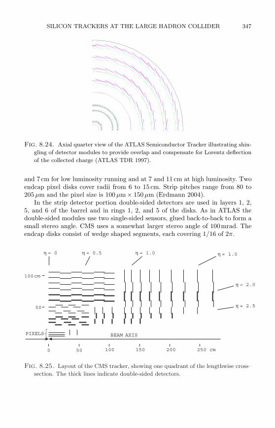
SILICON TRACKERS AT THE LARGE HADRON COLLIDER 347
Fig. 8.24. Axial quarter view of the ATLAS Semiconductor Tracker illustrating shin-
gling of detector modules to provide overlap and compensate for Lorentz deflection
of the collected charge (ATLAS TDR 1997).
and 7 cm for low luminosity running and at 7 and 11 cm at high luminosity. Twoendcap pixel disks cover radii from 6 to 15 cm. Strip pitches range from 80 to205 µm and the pixel size is 100 µm× 150 µm (Erdmann 2004).
In the strip detector portion double-sided detectors are used in layers 1, 2,5, and 6 of the barrel and in rings 1, 2, and 5 of the disks. As in ATLAS thedouble-sided modules use two single-sided sensors, glued back-to-back to form asmall stereo angle. CMS uses a somewhat larger stereo angle of 100mrad. Theendcap disks consist of wedge shaped segments, each covering 1/16 of 2π.
0 50 100 150 200 250 cm
50
100cm
BEAM AXIS
= 0 = 1.0 = 0.5 = 1.0
= 2.0
= 2.5
PIXELS
Fig. 8.25. Layout of the CMS tracker, showing one quadrant of the lengthwise cross–
section. The thick lines indicate double-sided detectors.
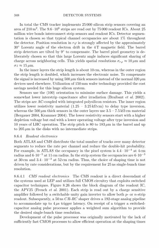
348 DETECTOR SYSTEMS
In total the CMS tracker implements 25 000 silicon strip sensors covering anarea of 210 m2. The 9.6 · 106 strips are read out by 75 000 readout ICs. About 25million wire bonds interconnect strip sensors and readout ICs. Detector segmen-tation is chosen so that typical channel occupancies are about 1% throughoutthe detector. Position resolution in rϕ is strongly affected by the approximately30 Lorentz angle of the electron drift in the 4T magnetic field. The barrelstrip detectors are tilted by 9 to compensate. The barrel pixel geometry is de-liberately chosen so that this large Lorentz angle induces significant sharing ofcharge across neighboring cells. This yields spatial resolutions σrϕ ≈ 10 µm andσz ≈ 15 µm.
In the inner layers the strip length is about 10 cm, whereas in the outer regionthe strip length is doubled, which increases the electronic noise. To compensatethe signal is increased by using 500µm thick sensors instead of the normal 320 µmdevices used elsewhere. Utilization of 150mm wafer technology provided the costsavings needed for this huge silicon system.
Sensors use the 〈100〉 orientation to minimize surface damage. This yields asomewhat lower interstrip capacitance after irradiation (Braibant et al. 2002).The strips are AC-coupled with integrated polysilicon resistors. The inner regionutilizes lower resistivity material (1.25 – 3.25 kΩ cm) to delay type inversion,whereas the 500 µm thick sensors in the outer layers use 3.5 – 7.5 kΩ cm material(Bergauer 2004, Krammer 2004). The lower resistivity sensors start with a higherdepletion voltage but end with a lower operating voltage after type inversion and10 years of LHC operation. The strip pitch is 80 to 183 µm in the barrel and upto 205 µm in the disks with no intermediate strips.
8.6.4 Readout electronics
Both ATLAS and CMS distribute the total number of tracks over many detectorsegments to reduce the rate per channel and reduce the double-hit probability.For example, in ATLAS the occupancy in the pixel system is 4.4 · 10−4 at 4 cmradius and 6·10−5 at 11 cm radius. In the strip system the occupancies are 6·10−3
at 30 cm and 3.4 · 10−3 at 52 cm radius. Thus, the choice of shaping time is notdriven by rate considerations, but by the requirement for 25 ns single-bunch timeresolution.
8.6.4.1 CMS readout electronics The CMS readout is a direct descendant ofthe systems used at LEP and utilizes full CMOS circuitry that exploits switchedcapacitor techniques. Figure 8.26 shows the block diagram of the readout IC,the APV25 (French et al. 2001). Each strip is read out by a charge sensitiveamplifier followed by a switchable unity gain inverter to allow both p- or n-stripreadout. Subsequently, a 50ns CR-RC shaper drives a 192-stage analog pipelineto accommodate up to 4 µs trigger latency. On receipt of a trigger a switched-capacitor analog pulse processor applies a weighted sum algorithm to providethe desired single-bunch time resolution.
Development of the pulse processor was originally motivated by the lack ofsufficiently fast CMOS processes to allow efficient operation at the shaping times
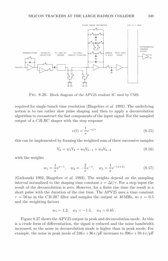
SILICON TRACKERS AT THE LARGE HADRON COLLIDER 349
PREAMPLIFIER
128 to 1 MUX
INPUT
PULSE SHAPE PROCESSOR
-1
SAMPLE& HOLD
POLARITYSELECTION
50 nsSHAPER
CR-RC 192-CELLANALOG PIPELINE
PROG GAINSTAGE
DIFFERENTIALCURRENTOUTPUT
Fig. 8.26. Block diagram of the APV25 readout IC used by CMS.
required for single-bunch time resolution (Bingefors et al. 1993). The underlyingnotion is to use rather slow pulse shaping and then to apply a deconvolutionalgorithm to reconstruct the fast components of the input signal. For the sampledoutput of a CR-RC shaper with the step response
v(t) =t
τe−t/τ (8.15)
this can be implemented by forming the weighted sum of three successive samples
Vk = w1Vk + w2Vk−1 + w3Vk−2 (8.16)
with the weights
w1 =1
xex−1, w2 = − 2
xe−1, w3 =
1
xe−(x+1) (8.17)
(Gadomski 1992, Bingefors et al. 1993). The weights depend on the samplinginterval normalized to the shaping time constant x = ∆t/τ . For a step input theresult of the deconvolution is zero. However, for a finite rise time the result is ashort pulse with the duration of the rise time. The APV25 uses a time constantτ = 50 ns in the CR-RC filter and samples the output at 40MHz, so x = 0.5and the weighting factors
w1 = 1.2, w2 = −1.5, w3 = 0.45 .
Figure 8.27 shows the APV25 output in peak and deconvolution mode. As thisis a crude form of differentiation, the signal is reduced and the noise bandwidthincreased, so the noise in deconvolution mode is higher than in peak mode. Forexample, the noise in peak mode of 246 e+36 e/pF increases to 396 e+59.4 e/pF

350 DETECTOR SYSTEMS
0 50 100 150 200 250
TIME (ns)
DECONVOLUTION
PEAK
Fig. 8.27. APV25 pulse shapes in peak and deconvolution mode, shown for input
capacitive loads ranging from 2 to 20.5 pF. The reduced pulse height at 17.5 and 20.5
pF indicates that the preamplifier bandwidth is becoming marginal. (Adapted from
Raymond al. 2000). Figure courtesy of M. Raymond.
in deconvolution mode. The latter is required for single-bunch timing resolutionat the LHC, so that is the relevant noise in normal operation.
Viewed somewhat differently, the CR-RC shaper is the anti-aliasing filterrequired before sampling the signal into the analog pipeline. The algorithm thenproduces a near triangular weighting function (Bingefors et al. 1993) with apeaking time of ∆t and the noise indices Fi = 0.35 and Fv = 1.84, similar to aconventional CR-RC3 or CR-RC4 filter.
The decision to utilize an all CMOS readout IC with the deconvolution pro-cessor was made early on and applied in a series of designs using different fabrica-tion processes. Fortuitously, the demonstration of excellent radiation resistancein standard commercial “deep sub-micron” CMOS opened the path to an effi-cient implementation in 0.25 µm CMOS (French et al. 2001). The APV25 chipcombines 128 readout channels with an output multiplexer and is 7.1mm wideand 8.1mm long (Raymond al. 2000).
The analog output signals are transmitted to the off-detector electronicsthrough optical links using edge-emitting semiconductor lasers operating at astandard telecommunications wavelength of 1310nm. Off-detector the opticalsignals are received by a photodiode-amplifier on the “front end driver”, whichdigitizes and processes the signals, subtracts pedestals and stores the results ina local memory. When operating at the maximum trigger rate, cluster finding isapplied to reduce the data volume.
8.6.4.2 ATLAS readout electronics ATLAS chose a readout system that soughtto efficiently balance the technology against cost, while meeting the physics re-quirements. The goal in these large systems is not to provide the best possible
SILICON TRACKERS AT THE LARGE HADRON COLLIDER 351
PREAMPLIFIER
DATA COMPRESSOR& SERIALIZER
INPUT
COMPARATOR 3.3 s DIGITAL PIPELINE
C
R
F
F
DACs &CALIBRATION LOGIC
THRESHOLD
EDGE SENSING &MASK REGISTER
DERANDOMIZER& BUFFER
COMMANDDECODER
READOUTCONTROLLER
READOUTLOGIC
CHOPPER TRIM DAC OUTPUT
128 PARALLEL SIGNAL CHANNELS
Fig. 8.28. Block diagram of the ABCD readout IC for the ATLAS SCT.
performance, but to maintain adequate performance over the lifetime of the de-tector. After a lengthy process of testing and comparing options, the collabora-tion concluded that these goals can be achieved by a binary readout, i.e. a systemthat just records the presence of a hit, so the output only provides a time stampwith a series of hit addresses. This technique also lends itself readily to on-chipzero-suppression, which reduces the cost and space requirements of the readoutlines. Threshold scans, as described in Section 4.7.3 and used in the BaBar SVT,allow pulse height measurements for diagnostics, but this is only necessary in-frequently to monitor changes in response, e.g. due to radiation damage. Figure8.28 shows the block diagram of the readout IC. The front-end utilizes time-invariant filtering. The bandwidths of the cascaded amplifiers needed to providethe necessary gain are tailored to provide approximately a CR-RC3 response.A comparator fires when a signal exceeds threshold and the time is stored in adigital pipeline, whose length accommodates the ATLAS level 1 trigger latency.Data sparsification and compression circuitry reduce the data volume that mustbe read out. More details follow in Section 8.6.4.4.
8.6.4.3 Required signal-to-noise ratio in a binary readout system Binary read-out systems were discussed in Section 4.7 of Chapter 4. The threshold must beset low enough to capture the desired portion of the amplitude spectrum, butnot so low that the rate of noise pulses is too high.
The signal for minimum ionizing particles is a Landau distribution, where for99% efficiency in a 300µm thick detector the threshold must be set to about onehalf the of the most probable charge Q0. Assume that the minimum signal tobe measured is fLQ0. Tracks passing between two strips will deposit charge onboth strips. The ability to distinguish one-hit from two-hit clusters improves theobtainable position resolution, as two-hit clusters are assigned mid-way betweentwo strips. If the fraction of the signal to be detected is fsh, the circuit must besensitive to signals as low as
352 DETECTOR SYSTEMS
Qmin = fshfLQ0 . (8.18)
As derived in Section 4.7, the required threshold-to-noise ratio for a noise occu-pancy Pn in a time interval ∆t is
QT
Qn=
√
−2 log
(
4√
3nTSPn
∆t
)
. (8.19)
In the strip system the average hit occupancy is about 5 · 10−3 in a time intervalof 25 ns. If we allow a noise occupancy of 10−3 at a shaping time of 20 ns, thiscorresponds to QT /Qn = 3.2.
The threshold uniformity is not perfect. The relevant measure is the thresholduniformity referred to the noise level. For a threshold variation ∆QT , the requiredthreshold-to-noise ratio becomes
QT
Qn=
√
−2 log
(
4√
3nTSPn
∆t
)
+∆QT
Qn. (8.20)
If ∆QT /Qn = 0.5, the required threshold-to-noise ratio becomes QT /Qn = 3.7.To maintain good timing, the signal must be above threshold by at least Qn, soQT /Qn > 4.7.
Combining the conditions for the threshold(
QT
Qn
)
min
Qn ≤ Qmin (8.21)
and signal (eqn 8.18)Qmin = fshfLQ0 (8.22)
yields the required noise level
Qn ≤ fshfLQ0
(QT /Qn)min. (8.23)
If charge sharing is negligible fsh = 1, so with fL = 0.5, Q0 = 3.5 fC, and(QT /Qn)min = 4.7, the required noise level Qn ≤ 0.37 fC or Qn ≤ 2300 e. Ifthe system is to operate with optimum position resolution, i.e. equal probabilityof one- and two-hit clusters, then fsh = 0.5 and Qn ≤ 0.19 fC or Qn ≤ 1150 e.ATLAS requires Qn ≤ 1500 e.
8.6.4.4 ATLAS SCT readout implementation ATLAS adopted a bipolar tran-sistor front-end with CMOS digital circuitry. Initial prototypes used separatebipolar and CMOS ICs. The production device utilizes a BiCMOS process thatcombines all of the circuitry in a single chip, the ABCD chip (Dabrowski etal. 2000, Campabadal et al. 2005a). Each chip includes 128 channels, on a6.4 × 4.5 mm2 die, bondable to a 50 µm pitch. Pitch adapters make the tran-sition to the detector strip pitch of 80µm. Designing the ICs for the smaller
SILICON TRACKERS AT THE LARGE HADRON COLLIDER 353
pitch provides space between adjacent ICs for bypass capacitors and wire bonds.The analog portion uses continuous shaping, approximating a CR-RC3 responsewith a peaking time of 20 ns. At the nominal operating threshold of 1 fC thisyields a time walk of 12 ns for signals of 1.2 to 10 fC. The double-pulse resolutionfor two successive 4 fC pulses is 50 ns. The operating current of the input tran-sistor is adjustable to optimize noise with radiation damage and the total poweris 1.3 to 1.8mW/ch.
On-chip DACs control the threshold and operating point. Trim DACs oneach channel fine tune the thresholds to compensate for threshold nonuniformityfrom channel to channel, bringing the threshold dispersion well below the noiselevel. This technique is even more important when power and readout area areminimized, as in pixel devices, so the efficacy of trimming will be illustrated inSection 8.6.7.
Each chip also includes digitally controlled calibration circuitry with a DAC-controlled injection level, shown in Figure 8.28. All control and output signals aredigital and each module communicates with the off-detector electronics throughoptical fibers. The serial link and token passing (see Figure 1.31) present single-point failure modes, so redundant readout modes are incorporated. In tokenpassing defective chips within a module can be bypassed. Normally, each modulehas two readout lines, one for each side. Should the master of one side fail, theother side’s master takes over and both sides are read out through one line.For a more detailed description of the ABCD readout IC see Campabadal et al.(2005a).
The adopted IC fabrication process was specially designed for LHC applica-tions and lacked a strong commercial base. Consequently, process control was notfully developed and the overall yield was about 20%. The project required about5 · 104 ICs, so this required a fast testing system, which was custom designed toprovide the necessary throughput to match the production schedule (Anghinolfiet al. 2002).
8.6.5 Detector modules
CMS uses a conventional module configuration with ceramic hybrids connectedat the ends of the detectors ATLAS adopted a novel module design, so it will bediscussed in more detail. Figure 8.29 shows the module layout. Connecting theelectronics at the mid-point of the barrel modules reduces the noise contributionof the strip resistance, as discussed in Section 6.5. The electronics hybrid uses afour-layer polyimide substrate shown in Figure 8.30 (Kondo 2002 et al., Kohrikiet al. 2002). This reduces material and also allows the electronics for both sidesto be placed on the same layer, as the hybrid can be wrapped around the detector(Figure 8.31). A close up of the ICs mounted on the hybrid is shown in Chapter1 (Figure 1.33).
Two single-sided p-on-n sensors are glued back to back to form a 40mradstereo angle. Each sensor has 784 strips on an 80µm pitch. Two sensors arebutted to provide an overall strip length of 126mm. An intermediate baseboard of
354 DETECTOR SYSTEMS
HYBRID ASSEMBLY
BeO FACINGS
SLOTTED W ASHER
SILICON SENSORS
BASEBOARD TPG
DATUM W ASHER
BeO FACINGS
CONNECTOR
Fig. 8.29. ATLAS SCT barrel detector module. Two single-sided sensors are glued
back-to-back with an intermediate TPG heat spreader. The “ear” extending from
the module attaches to the support/cooling stave of the SCT barrel structure.
(Figure courtesy of T. Kondo.)
thermalized pyrolytic graphite (TPG) provides support and a high-conductivitycooling path to the mounting stave of the barrel support structure. The hybridis mounted on spacers to prevent direct heat transfer from the readout ICs tothe sensors. This bridge configuration and the high thermal conductivity of theTPG heat spreader between the sensors ensures that the sensors are cooledsufficiently to limit anti-annealing and thermal runaway after radiation damage.Results of a finite element thermal simulation are shown in Figure 8.32 (Kondoet al. 2002). The disk modules use a similar structure, but the electronics are endmounted (Moorhead 2002, Feld 2003, Nisius 2004). Table 8.2 lists contributionsto the material of a barrel module. At normal incidence the detector modules,
Fig. 8.30. SCT front-end ICs and associated components are mounted on a flex
hybrid that wraps around the module. The hybrid integrates electronics, intercon-
nections and the connector for both sides. Bypass capacitors are visible adjacent to
each IC and off the ends of the two arrays of readout ICs. (Photograph courtesy of
T. Kondo.)
SILICON TRACKERS AT THE LARGE HADRON COLLIDER 355
Table 8.2 Material in an SCT module, expressedin percent of a radiation length X0.
Silicon sensors and adhesive 0.612
Baseboard and BeO facings 0.194
ICs and adhesive 0.063
Cu/polyimide hybrid 0.221
Passive components 0.076
Total 1.17% X0
the cooling and support structure, and the cabling in the four-layer tracker addup to 0.1 X0.
Electrical signals are transmitted by fully balanced LVDS links. Noise pickupfrom the digital electronics to the sensors is negligible and modules operating insystems mock-ups show negligible common mode noise and no cross-talk (Ferrari2004). Figure 8.33 shows a photograph of an assembled module. For a summaryof test beam results see Campabadal et al. (2005b).
The scale of these projects does not allow the improvisation and last minutecrash programs that characterize smaller projects. Small projects can make lastminute changes and implement them rather quickly. Small systems also tend tobe more accessible, so after some initial running it is common to take them outfor rework. In huge detectors like ATLAS and CMS removing the silicon systemsis a major effort that necessitates significant downtime. Thus the reliability re-quirements are similar to systems in space. Both ATLAS and CMS have adopted
READOUT ICs
BeO FACING (0.25)AIR GAP (0.4)
Cu-POLYIMIDE FLEXIBLE CIRCUIT (0.27)
SILICON SENSORS (0.285)
TPG HEAT SPREADER (0.38)WITH EPOXY COATING (0.02)
CARBON-CARBON BRIDGE (0.3)WITH PARYLENE COATING (0.01)
CONNECTORCOOLING BLOCK
10mm
1mm
Fig. 8.31. Schematic cross-section of an SCT barrel module (vertical scale exagger-
ated). The hybrid is glued to a bridge to reduce heat transfer to the sensors. The
height of the bridge still allows reliable wire bonding to the sensors. Thicknesses
(in parenthesis) are in mm. (Figure courtesy of T. Kondo.)
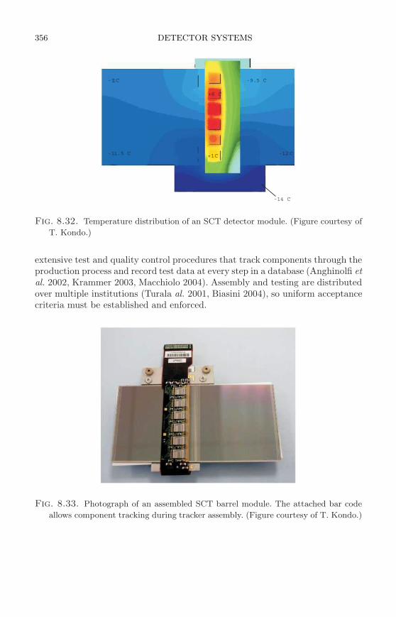
356 DETECTOR SYSTEMS
+6 C
-14 C
-9.5 C
+1C
-11C
-11.5 C -12C
Fig. 8.32. Temperature distribution of an SCT detector module. (Figure courtesy of
T. Kondo.)
extensive test and quality control procedures that track components through theproduction process and record test data at every step in a database (Anghinolfi etal. 2002, Krammer 2003, Macchiolo 2004). Assembly and testing are distributedover multiple institutions (Turala al. 2001, Biasini 2004), so uniform acceptancecriteria must be established and enforced.
Fig. 8.33. Photograph of an assembled SCT barrel module. The attached bar code
allows component tracking during tracker assembly. (Figure courtesy of T. Kondo.)
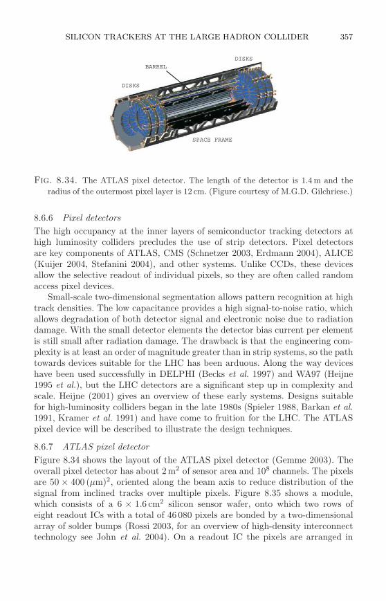
SILICON TRACKERS AT THE LARGE HADRON COLLIDER 357
DISKS
BARREL
SPACE FRAME
DISKS
Fig. 8.34. The ATLAS pixel detector. The length of the detector is 1.4 m and the
radius of the outermost pixel layer is 12 cm. (Figure courtesy of M.G.D. Gilchriese.)
8.6.6 Pixel detectors
The high occupancy at the inner layers of semiconductor tracking detectors athigh luminosity colliders precludes the use of strip detectors. Pixel detectorsare key components of ATLAS, CMS (Schnetzer 2003, Erdmann 2004), ALICE(Kuijer 2004, Stefanini 2004), and other systems. Unlike CCDs, these devicesallow the selective readout of individual pixels, so they are often called randomaccess pixel devices.
Small-scale two-dimensional segmentation allows pattern recognition at hightrack densities. The low capacitance provides a high signal-to-noise ratio, whichallows degradation of both detector signal and electronic noise due to radiationdamage. With the small detector elements the detector bias current per elementis still small after radiation damage. The drawback is that the engineering com-plexity is at least an order of magnitude greater than in strip systems, so the pathtowards devices suitable for the LHC has been arduous. Along the way deviceshave been used successfully in DELPHI (Becks et al. 1997) and WA97 (Heijne1995 et al.), but the LHC detectors are a significant step up in complexity andscale. Heijne (2001) gives an overview of these early systems. Designs suitablefor high-luminosity colliders began in the late 1980s (Spieler 1988, Barkan et al.1991, Kramer et al. 1991) and have come to fruition for the LHC. The ATLASpixel device will be described to illustrate the design techniques.
8.6.7 ATLAS pixel detector
Figure 8.34 shows the layout of the ATLAS pixel detector (Gemme 2003). Theoverall pixel detector has about 2 m2 of sensor area and 108 channels. The pixelsare 50 × 400 (µm)2, oriented along the beam axis to reduce distribution of thesignal from inclined tracks over multiple pixels. Figure 8.35 shows a module,which consists of a 6 × 1.6 cm2 silicon sensor wafer, onto which two rows ofeight readout ICs with a total of 46 080 pixels are bonded by a two-dimensionalarray of solder bumps (Rossi 2003, for an overview of high-density interconnecttechnology see John et al. 2004). On a readout IC the pixels are arranged in
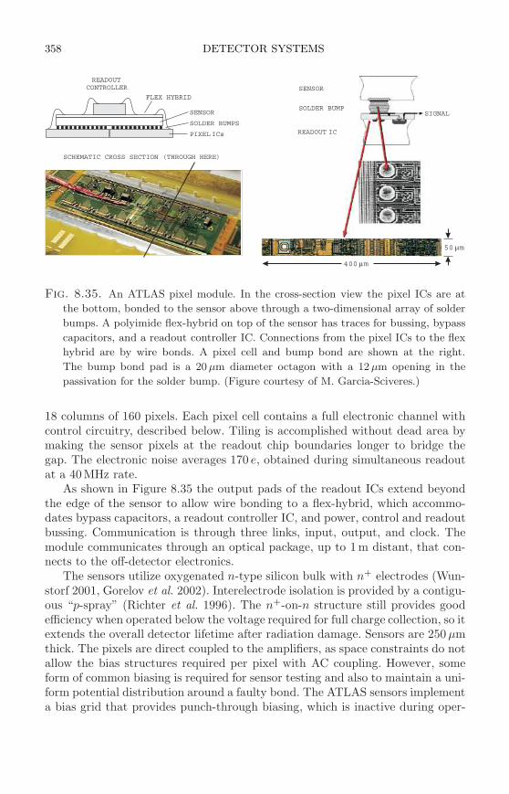
358 DETECTOR SYSTEMS
PIXEL ICs
SOLDER BUMPS
SENSOR
FLEX HYBRID
READOUTCONTROLLER
SCHEMATIC CROSS SECTION (THROUGH HERE)
SENSOR
SOLDER BUMP
READOUT IC
SIGNAL
400 m
50 m
Fig. 8.35. An ATLAS pixel module. In the cross-section view the pixel ICs are at
the bottom, bonded to the sensor above through a two-dimensional array of solder
bumps. A polyimide flex-hybrid on top of the sensor has traces for bussing, bypass
capacitors, and a readout controller IC. Connections from the pixel ICs to the flex
hybrid are by wire bonds. A pixel cell and bump bond are shown at the right.
The bump bond pad is a 20 µm diameter octagon with a 12 µm opening in the
passivation for the solder bump. (Figure courtesy of M. Garcia-Sciveres.)
18 columns of 160 pixels. Each pixel cell contains a full electronic channel withcontrol circuitry, described below. Tiling is accomplished without dead area bymaking the sensor pixels at the readout chip boundaries longer to bridge thegap. The electronic noise averages 170 e, obtained during simultaneous readoutat a 40MHz rate.
As shown in Figure 8.35 the output pads of the readout ICs extend beyondthe edge of the sensor to allow wire bonding to a flex-hybrid, which accommo-dates bypass capacitors, a readout controller IC, and power, control and readoutbussing. Communication is through three links, input, output, and clock. Themodule communicates through an optical package, up to 1 m distant, that con-nects to the off-detector electronics.
The sensors utilize oxygenated n-type silicon bulk with n+ electrodes (Wun-storf 2001, Gorelov et al. 2002). Interelectrode isolation is provided by a contigu-ous “p-spray” (Richter et al. 1996). The n+-on-n structure still provides goodefficiency when operated below the voltage required for full charge collection, so itextends the overall detector lifetime after radiation damage. Sensors are 250µmthick. The pixels are direct coupled to the amplifiers, as space constraints do notallow the bias structures required per pixel with AC coupling. However, someform of common biasing is required for sensor testing and also to maintain a uni-form potential distribution around a faulty bond. The ATLAS sensors implementa bias grid that provides punch-through biasing, which is inactive during oper-
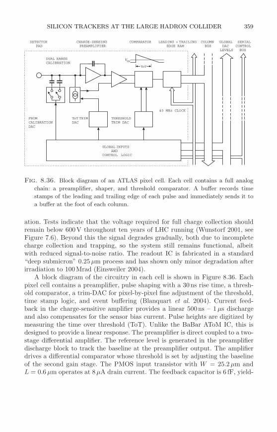
SILICON TRACKERS AT THE LARGE HADRON COLLIDER 359
FROMCALIBRATIONDAC
ToT TRIMDAC
THRESHOLDTRIM DAC
40 MHz CLOCK
LEADING + TRAILINGEDGE RAM
COMPARATORCHARGE-SENSINGPREAMPLIFIER
COLUMNBUS
GLOBAL INPUTSAND
CONTROL LOGIC
ToT
VTH
DETECTORPAD
DUAL RANGECALIBRATION
GLOBALDAC
LEVELS
SERIALCONTROLBUS
Fig. 8.36. Block diagram of an ATLAS pixel cell. Each cell contains a full analog
chain: a preamplifier, shaper, and threshold comparator. A buffer records time
stamps of the leading and trailing edge of each pulse and immediately sends it to
a buffer at the foot of each column.
ation. Tests indicate that the voltage required for full charge collection shouldremain below 600V throughout ten years of LHC running (Wunstorf 2001, seeFigure 7.6). Beyond this the signal degrades gradually, both due to incompletecharge collection and trapping, so the system still remains functional, albeitwith reduced signal-to-noise ratio. The readout IC is fabricated in a standard“deep submicron” 0.25 µm process and has shown only minor degradation afterirradiation to 100Mrad (Einsweiler 2004).
A block diagram of the circuitry in each cell is shown in Figure 8.36. Eachpixel cell contains a preamplifier, pulse shaping with a 30ns rise time, a thresh-old comparator, a trim-DAC for pixel-by-pixel fine adjustment of the threshold,time stamp logic, and event buffering (Blanquart et al. 2004). Current feed-back in the charge-sensitive amplifier provides a linear 500ns – 1µs dischargeand also compensates for the sensor bias current. Pulse heights are digitized bymeasuring the time over threshold (ToT). Unlike the BaBar AToM IC, this isdesigned to provide a linear response. The preamplifier is direct coupled to a two-stage differential amplifier. The reference level is generated in the preamplifierdischarge block to track the baseline at the preamplifier output. The amplifierdrives a differential comparator whose threshold is set by adjusting the baselineof the second gain stage. The PMOS input transistor with W = 25.2 µm andL = 0.6 µm operates at 8 µA drain current. The feedback capacitor is 6 fF, yield-
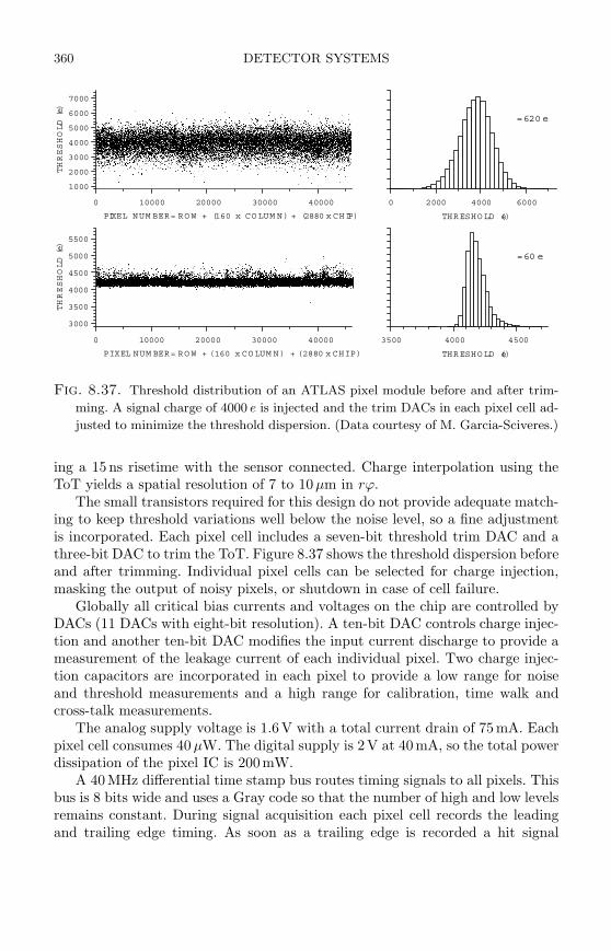
360 DETECTOR SYSTEMS
0 10000 20000 30000 40000
PIXEL NUM BER = ROW + (160 x CO LUM N) + (2880 x CHIP)
1000
2000
3000
4000
5000
6000
7000
THRESHOLD(e)
0 2000 4000 6000
THRESHO LD (e)
0 10000 20000 30000 40000
PIXEL NUM BER = RO W + (160 x CO LUM N) + (2880 x CHIP)
3000
3500
4000
4500
5000
5500
THRESHOLD(e)
3500 4000 4500
THRESHO LD (e)
=620 e
=60 e
Fig. 8.37. Threshold distribution of an ATLAS pixel module before and after trim-
ming. A signal charge of 4000 e is injected and the trim DACs in each pixel cell ad-
justed to minimize the threshold dispersion. (Data courtesy of M. Garcia-Sciveres.)
ing a 15ns risetime with the sensor connected. Charge interpolation using theToT yields a spatial resolution of 7 to 10µm in rϕ.
The small transistors required for this design do not provide adequate match-ing to keep threshold variations well below the noise level, so a fine adjustmentis incorporated. Each pixel cell includes a seven-bit threshold trim DAC and athree-bit DAC to trim the ToT. Figure 8.37 shows the threshold dispersion beforeand after trimming. Individual pixel cells can be selected for charge injection,masking the output of noisy pixels, or shutdown in case of cell failure.
Globally all critical bias currents and voltages on the chip are controlled byDACs (11 DACs with eight-bit resolution). A ten-bit DAC controls charge injec-tion and another ten-bit DAC modifies the input current discharge to provide ameasurement of the leakage current of each individual pixel. Two charge injec-tion capacitors are incorporated in each pixel to provide a low range for noiseand threshold measurements and a high range for calibration, time walk andcross-talk measurements.
The analog supply voltage is 1.6V with a total current drain of 75mA. Eachpixel cell consumes 40µW. The digital supply is 2V at 40mA, so the total powerdissipation of the pixel IC is 200mW.
A 40MHz differential time stamp bus routes timing signals to all pixels. Thisbus is 8 bits wide and uses a Gray code so that the number of high and low levelsremains constant. During signal acquisition each pixel cell records the leadingand trailing edge timing. As soon as a trailing edge is recorded a hit signal
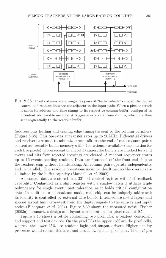
SILICON TRACKERS AT THE LARGE HADRON COLLIDER 361
COLUMNBUFFERS
PIXELCELLS
CONTENTADDRESSABLE
MEMOR Y
CONTENTADDRESSABLE
MEMOR Y
TRIGGER
DATA OUT
Fig. 8.38. Pixel columns are arranged as pairs of “back-to-back” cells, so the digital
control and readout lines are not adjacent to the input pads. When a pixel is struck
it sends its address and time stamp to its respective column buffer, configured as
a content addressable memory. A trigger selects valid time stamps, which are then
sent sequentially to the readout buffer.
(address plus leading and trailing edge timing) is sent to the column periphery(Figure 8.38). This operates at transfer rates up to 20MHz. Differential driversand receivers are used to minimize cross-talk. At the end of each column pair acontent addressable buffer memory with 64 locations is available (one location foreach five pixels). Upon receipt of a level 1 trigger, the buffers are checked for validevents and hits from rejected crossings are cleared. A readout sequencer storesup to 16 events pending readout. Data are “pushed” off the front-end chip tothe readout chip without handshaking. All column pairs operate independentlyand in parallel,. The readout operations incur no deadtime, so the overall rateis limited by the buffer capacity (Mandelli et al. 2002).
All control data are stored in a 231-bit control register with full readbackcapability. Configured as a shift register with a shadow latch it utilizes tripleredundancy for single event upset tolerance, as it holds critical configurationdata. In addition to a broadcast mode, each chip can be uniquely addressed;its identity is controlled by external wire bonds. Intermediate metal layers andspecial layout limit cross-talk from the digital signals to the sensors and inputnodes (Blanquart et al. 2004). Figure 8.39 shows the measured noise. Fischer(2003a) summarizes design and layout considerations for pixel readout ICs.
Figure 8.40 shows a reticle containing two pixel ICs, a readout controller,and support and test devices. On the pixel ICs the upper 75% are the pixel cells,whereas the lower 25% are readout logic and output drivers. Higher densityprocesses would reduce this area and also allow smaller pixel cells. The 0.25 µm
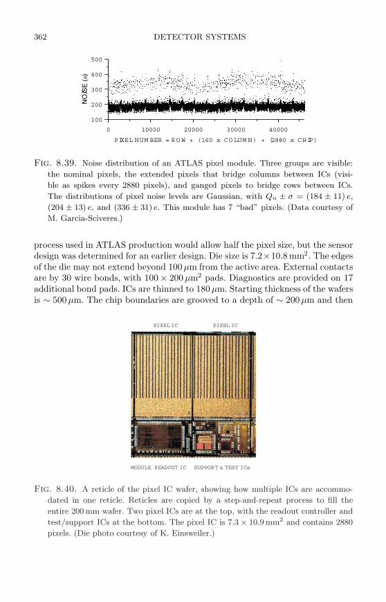
362 DETECTOR SYSTEMS
0 10000 20000 30000 40000
PIXEL NUM BER = ROW + (160 x COLUM N) + (2880 x CHIP)
100
200
300
400
500
NOISE(e)
Fig. 8.39. Noise distribution of an ATLAS pixel module. Three groups are visible:
the nominal pixels, the extended pixels that bridge columns between ICs (visi-
ble as spikes every 2880 pixels), and ganged pixels to bridge rows between ICs.
The distributions of pixel noise levels are Gaussian, with Qn ± σ = (184 ± 11) e,
(204 ± 13) e, and (336 ± 31) e. This module has 7 “bad” pixels. (Data courtesy of
M. Garcia-Sciveres.)
process used in ATLAS production would allow half the pixel size, but the sensordesign was determined for an earlier design. Die size is 7.2×10.8 mm2. The edgesof the die may not extend beyond 100 µm from the active area. External contactsare by 30 wire bonds, with 100× 200 µm2 pads. Diagnostics are provided on 17additional bond pads. ICs are thinned to 180 µm. Starting thickness of the wafersis ∼ 500 µm. The chip boundaries are grooved to a depth of ∼ 200 µm and then
MODULE READOUT IC SUPPORT & TEST ICs
PIXEL IC PIXEL IC
Fig. 8.40. A reticle of the pixel IC wafer, showing how multiple ICs are accommo-
dated in one reticle. Reticles are copied by a step-and-repeat process to fill the
entire 200 mm wafer. Two pixel ICs are at the top, with the readout controller and
test/support ICs at the bottom. The pixel IC is 7.3 × 10.9 mm2 and contains 2880
pixels. (Die photo courtesy of K. Einsweiler.)
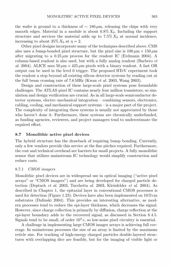
MONOLITHIC ACTIVE PIXEL DEVICES 363
the wafer is ground to a thickness of ∼ 180 µm, releasing the chips with verysmooth edges. Material in a module is about 0.8% X0. Including the supportstructure and services the material adds up to 7.5% X0 at normal incidence,increasing to about 35% X0 at η = 2.
Other pixel designs incorporate many of the techniques described above. CMSalso uses a bump-bonded pixel structure, but the pixel size is 100 µm × 150 µmafter migrating to a 0.25 µm process for the readout IC (Erdmann 2004). Acolumn-based readout is also used, but with a fully analog readout (Barbero etal. 2004). ALICE uses 50 µm × 425 µm pixels with a binary readout. A fast ORoutput can be used in the level 0 trigger. The proposed BTeV experiment tookthe readout a step beyond all existing silicon detector systems by reading out atthe full beam crossing rate of 7.6 MHz (Kwan et al. 2003, Wang 2003).
Design and construction of these large-scale pixel systems pose formidablechallenges. The ATLAS pixel IC contains nearly four million transistors, so sim-ulation and design verification are crucial. As in all large-scale semiconductor de-tector systems, electro–mechanical integration – combining sensors, electronics,cabling, cooling, and mechanical support systems – is a major part of the project.The complexity of integrating these systems is usually not appreciated by thosewho haven’t done it. Furthermore, these systems are chronically underfunded,as funding agencies, reviewers, and project managers tend to underestimate therequired effort.
8.7 Monolithic active pixel devices
The hybrid structure has the drawback of requiring bump bonding. Currently,only a few vendors provide this service at the fine pitches required. Furthermore,the cost and technical overhead are barriers for small projects. A fully monolithicsensor that utilizes mainstream IC technology would simplify construction andreduce costs.
8.7.1 CMOS imagers
Monolithic pixel devices are in widespread use in optical imaging (“active pixelarrays” or “CMOS imagers”) and are being developed for charged particle de-tection (Deptuch et al. 2003, Turchetta al. 2003, Kleinfelder et al. 2004). Asdescribed in Chapter 1, the epitaxial layer in conventional CMOS processes isused for detection (Figure 1.23). Devices have also been implemented on 10 Ω cmsubstrates (Dulinski 2004). This provides an interesting alternative, as mod-ern processes tend to reduce the epi-layer thickness, which decreases the signal.However, since charge collection is primarily by diffusion, charge reflection at theepi-layer boundary adds to the recovered signal, as discussed in Section 8.4.5.Signals tend to be small, of order 103 e, so low-noise pixel circuitry is essential.
A challenge in implementing large CMOS imager arrays is achieving full cov-erage. In mainstream processes the size of an array is limited by the maximumreticle size. For tracking of high-energy charged particles double-layered struc-tures with overlapping dice are feasible, but for the imaging of visible light or
364 DETECTOR SYSTEMS
p ppp ++ n n n+ + +
n
OHMIC CONTACT
INTERNAL GATE
S D
CONTROLGATE
n
CLEAR BULK
ROTATIONALSYMMETR Y
AXIS
ROWSELECT
OFF
ON
OFF
OFF
PIXEL MATRIX
OUTPUTS
Fig. 8.41. DEPFET structure (left) and readout matrix (right). The second row is
selected for readout and all outputs are available. The control and signal paths are
shown for the second pixel.
soft x-rays the dead area of the front IC blocks the active area of the one behind.The gap between dice can be reduced by including multiple reticles in one die.With some compromises in layout, circuitry might also be “stitched” to formcontiguous multireticle ICs. However, both techniques are limited by yield.
This is a very active area and the limits of the technology are still beingexplored. Adequate signal-to-noise ratios for particle tracking have been demon-strated and designs for full systems are underway, especially targeting linearcollider applications. In those applications that require sparsified readout, thecircuit complexity will be similar to the ATLAS pixel readout described above.
The charge collection mechanism limits the radiation resistance of these de-vices. As charge collection is primarily by diffusion, the magnitude of the signal issensitive to minority carrier lifetime (Appendix F), especially since the injectedcharge concentration is low. Displacement damage will reduce the minority car-rier lifetime to 10ns after exposure to a hadron fluence of order 1013 cm−2, scalinginversely proportional to fluence (Messenger and Ash 1986). Since the diffusiontime is of order 100ns, this limits the application of these devices to less severeenvironments.
8.7.2 DEPFET pixel detectors
The simplest active pixel device is an array of transistors. A novel implementa-tion that integrates the sensor and transistor monolithically is the “DEPFET”structure (Kemmer and Lutz 1987, Richter al. 2003). The DEPFET combines thefunctions of a charge collecting electrode and an FET. The structure is shown inthe left panel of Figure 8.41. The p-channel JFET can be controlled by two gateelectrodes. The upper gate is used to activate the device. The buried gate senses
ASTRONOMICAL IMAGING 365
the signal charge. Through a combination of doping and biasing a potential wellis formed at the buried gate so that signal electrons from the associated pixelvolume will collect there, regardless of whether the FET is activated or not.
For readout the DEPFETs are configured as a matrix, as shown in the secondpanel of Figure 8.41. All control gates in a row are bussed, as are all collectors in acolumn. By switching the gates on, all FETs in the corresponding row become thefirst stage of a readout amplifier that drives the external second amplifier stagethrough the common output bus. The first and second stages are convenientlyconfigured as a cascode. After readout the internal gate is discharged, by forwardbiasing either the clear electrode or the control gate. Discharge is not alwayscomplete and the reset itself can introduce baseline shifts, so the residual baselinemust be recorded and subtracted from the next readout (Fischer et al. 2003b).
The absence of external connections to the input node reduces stray ca-pacitance and the low input capacitance yields low equivalent noise charge. Inmatrices operated with 50 kHz line rates a noise level of 2.2 eV has been achievedwith 131 eV resolution for 5.9 keV x-rays. The key parameter is the conversion ofsignal charge qs to output current gq = ∆ID/∆qs. Values of 200 pA/e are typi-cal (Fischer et al. 2003b) and as high as 400 pA/e have been reported (Wermes2004). This is to be compared to a MOSFET’s gm/Ci, which in modern devicescan be significantly higher, even for low-power operating points (see Chapter 6).
Obtainable noise levels and full frame readout rates are comparable to CCDs.Similarly, since charge is stored when the device is inactive, applications withlow frame rates require very low power. Common to both is that the shot noisedepends on the exposure time between readouts. During an exposure time T thesensor dark current Id accumulates IdT/e electrons, so the shot noise
Qni =
√
IdT
e(8.24)
is independent of the external pulse shaper. However, the voltage noise con-tributions from the front-end transistor, series resistances, etc. depend on thebandwidth of the signal processing chain.
Both DEPFETs and CCDs can be implemented on fully depleted substrateswith hundreds of µm thickness (fully depleted CCDs are described below), soachievable signal levels are comparable. Both utilize specialized processes that arenot constrained by the die size of commercial CMOS, so large devices are possible,as described in Section 8.4.5. Unlike CCDs, DEPFET readout is nondestructiveand pixels can be addressed individually, so selected fields can be read out rapidlywhile continuing to integrate the full field. Readout also proceeds without thedata moving through the image frame. DEPFET structures have been studied forx-ray astronomy (Holl 2000), tritium autoradiography in biomedical applications(Ulrici 2004), and vertex detectors for linear colliders (Trimpl 2003).
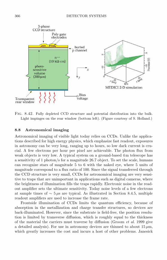
366 DETECTOR SYSTEMS
Fig. 8.42. Fully depleted CCD structure and potential distribution into the bulk.
Light impinges on the rear window (bottom left). (Figure courtesy of S. Holland.)
8.8 Astronomical imaging
Astronomical imaging of visible light today relies on CCDs. Unlike the applica-tions described for high energy physics, which emphasize fast readout, exposuresin astronomy can be very long, ranging up to hours, so low dark current is cru-cial. A few electrons per hour per pixel are achievable. The photon flux fromweak objects is very low. A typical system on a ground-based 4m telescope hasa sensitivity of 1 photon/s for a magnitude 26.7 object. To set the scale, humanscan recognize stars of magnitude 5 to 6 with the naked eye, where 5 units ofmagnitude correspond to a flux ratio of 100. Since the signal transferred throughthe CCD structure is very small, CCDs for astronomical imaging are very sensi-tive to traps that are unimportant in applications such as digital cameras, wherethe brightness of illumination fills the traps rapidly. Electronic noise in the read-out amplifier sets the ultimate sensitivity. Today noise levels of a few electronsat sample times of ∼ 5 µs are typical. As illustrated in Section 8.4.5, multiplereadout amplifiers are used to increase the frame rate.
Frontside illumination of CCDs limits the quantum efficiency, because ofabsorption in the metallization and charge transfer structures, so devices areback-illuminated. However, since the substrate is field-free, the position resolu-tion is limited by transverse diffusion, which is roughly equal to the thicknessof the material the carriers must traverse by diffusion (Groom et al. 1999 givea detailed analysis). For use in astronomy devices are thinned to about 15µm,which greatly increases the cost and incurs a host of other problems. Janesick
EMERGING APPLICATIONS 367
(2000) gives a comprehensive description of CCD technology and systems forastronomical imaging, so only one novel development will be described here toindicate how disparate fields can benefit from one another.
The CCDs used in high energy physics are adaptations of devices developedfor other applications. Conversely, technologies developed in the course of genericdetector R&D for high energy physics have enabled a new class of CCDs forastronomy and other applications.
The first ingredient was the monolithic integration of high-quality detectorsand electronics on high-resistivity, fully depleted substrates (Holland and Spieler1990, Holland 1992). Although portrayed in Chapter 1 as an evolutionary “deadend” for detectors with complex readouts, this technology is well-matched toCCDs.
The second ingredient was to adapt the technology to photodiode arrays. Thebackside gettering layer provided the low dark current required, but the backsidedead layers had to be thinned substantially to obtain high quantum efficiency inthe visible. The impetus for this development came from medical imaging andwas implemented in the course of developing the photodiode arrays in the PETsystem whose readout was described in Chapter 4 (Choong et al. 2002, Holland,Wang, and Moses 1997).
Unlike conventional CCDs that use a p-substrate and transport electrons, thisdevice uses an n-substrate and transports holes. The substrate is fully depletedby an applied bias (Holland et al. 2003). Figure 8.42 shows the structure andpotential distribution. The applied field speeds up collection time, which limitstransverse diffusion; at 30V bias voltage the transverse diffusion is about 10 µmrms (Karcher et al. 2004).
For astronomical observations the 300 µm depletion depth has the very im-portant advantage of improving the red response, as shown in Figure 8.43. Sincethe interstellar dust absorbs in the blue, the extended red response significantlyenhances imaging sensitivity (Groom 2000, Holland et al. 2003). Radiation re-sistance is also good; devices have been tested to fluences of 1011 cm−2 12MeVprotons (Bebek et al. 2002).
8.9 Emerging applications
8.9.1 Space applications
CCDs are at the heart of the Hubble Space Telescope and larger arrays will beused in future faint light imagers in space. The fully depleted CCDs describedabove are the enabling technology for a proposed satellite observatory, the Super-Nova Acceleration Probe (SNAP) (Linder 2002, Aldering 2004). A typical focalplane design includes 36 2K× 2K HgCdTe near infrared sensors with 18 µm pix-els and 36 3.5K× 3.5K CCDs with 10.5 µm pixels to cover the visible spectrum.The complete focal plane would be cooled to 140 K. Packaging is a major chal-lenge. The 200 – 300µm fully depleted CCDs are self-supporting, so single devicescan be mounted on a “window frame” made of aluminum-nitride, which closely
368 DETECTOR SYSTEMS
300 400 500 600 700 800 900 1000 1100WAVELENGTH (nm )
0
20
40
60
80
100
QUANTUMEFFICIENCY(%
)THINNED
FULL DEPLDEEPDEPL
Fig. 8.43. Quantum efficiency of a thinned CCD, a deep depletion CCD (high resis-
tivity substrate, partially depleted), and a fully depleted CCD with 300 µm sensitive
thickness. (Data courtesy of S. Holland)
matches silicon’s thermal expansion. However, the width of the frame is not suit-able for a densely packed array. In a higher density package the CCD is gluedwith the circuit side down to a contiguous aluminum-nitride carrier. The CCDextends beyond the carrier, so the bond pads are accessible to make connectionsto traces on the backside of the carrier, which also accommodates bypass capac-itors, heater resistors, and a connector for the readout cable. (Stover al. 2004).The large-scale readout utilizes custom-designed ICs and builds on experiencefrom high energy physics.
X-ray detectors are important for both cosmological surveys and the study ofblack holes. Some desired characteristics are summarized by Remillard (2004).In the soft and medium x-ray band (0.5 – 15 keV), for example, the detectorgoals include a pixel size of 20µm, spectral resolution of 2 keV at 6 keV, a timeresolution of 100 µs, and a count rate capability of 104 s−1. No single detectortechnology offers the prospect of meeting all of these goals. Gas counters andCCDs are commonly used, but enhanced CCDs or hybrid pixel arrays can im-prove substantially on current capabilities. However, this will require substantialdevelopment.
Large silicon arrays are integral to a new space-based gamma-ray telescope.The Gamma-ray Large Area Space Telescope (GLAST) utilizes stacks of alter-nating conversion foils and silicon strip detectors to track gamma-rays in therange of 20 – > 300GeV (Attwood 1994, Morselli 2004). Figure 8.44 shows theprinciple. The tracker consists of 16 square towers about 37 cm on a side and60 cm high. The modular design utilizes individual trays that are stacked to forma tower (Bellazini et al. 2003). As shown in Figure 8.45 each tray includes twolayers of single-sided strip sensors with a 90 stereo angle, a tungsten converterfoil, and a multichip module with 24 readout ICs and a readout controller. An
EMERGING APPLICATIONS 369
e e+
ANTI-COINCIDENCESHIELD
CONVERSION FOIL
SENSOR LAYER
CALORIMETER
Fig. 8.44. Incident gamma-rays produce e+e− pairs in converter foils and the tra-
jectories of the particles are measured in a silicon strip tracker.
aluminum honeycomb with carbon-carbon facings provides rigidity. The totalweight of the 16 tracker towers is 500kg.
By the standards of high energy physics the technology is conventional, butit is quite novel for NASA. The detectors are fabricated on 150mm wafers. Foursensor wafers are ganged to form a 36 cm long ladder read out at one end. Fourladders comprise the active area of a layer and 36 layers (18 x-y pairs) per towerprovide sufficient redundancy to tolerate the loss of a few layers. Building onexperience from BaBar, the readout consumes only 190µW per channel at anoise level that ensures a noise occupancy < 10−4 per trigger. The total powerdissipation of the 24 front-end ICs and the readout controller on the readouthybrid is 0.25W. With a strip pitch of 228 µm the tracker has nearly 9 · 105
channels and consumes less than 160W.The silicon tracker is an international collaboration with key fabrication and
assembly steps in Italy (tower assembly), Japan (sensors), and the U.S. (elec-tronics and final integration). Sensor design builds on extensive experience fromhigh energy physics (Ohsugi et al. 1999). Detector performance is excellent; mea-surements on 600 ladders after assembly show average bias currents of 600nAper ladder with an rms spread of 200nA (Latronico 2004). Only 105 of 1.1 · 107
strips didn’t meet specifications, i.e. a rejection rate of 10−5 (Bellazini et al.2003). All communication between ICs and with the external readout electronicsis by current balanced LVDS, which yields very low cross-talk and no measurableelectromagnetic radiation, even without shielding (Nelson 2004).
8.9.2 X-ray imaging and spectroscopy
X-ray imaging and energy spectroscopy are important in many areas. However,their requirements differ significantly from high energy physics or x-ray astron-
370 DETECTOR SYSTEMS
omy. Unlike tracking devices in high energy physics, which require low noiseto obtain a high detection efficiency of a broad energy distribution, x-ray spec-troscopy demands precision pulse-height measurements, often at high fluctuatingrandom rates that require excellent instantaneous baseline control. This also setsthem apart from x-ray astronomy, which requires high energy resolution, but atrather low rates. Image fields are filled, so the frame rate cannot be increasedby on-chip sparsification. The required trade-off between energy selectivity andrate capability depends greatly on the application. Digital imaging, i.e. photoncounting, lessens the requirements on energy precision, but still requires energywindowing to reduce backgrounds. Integrating detectors are also widely used.This is one area where amorphous silicon arrays are useful, as the total signal islarger than in single photon counting. In contrast, precision x-ray spectroscopyoften requires resolution of weak lines adjacent to strong lines, so full chargecollection in the sensor is essential to reduce low-energy “tails”, as is precisionbaseline control under random rates. Figure 4.18 in Chapter 4 illustrates the re-quired performance. Hybrid pixel arrays offer great promise in this application,as the sensor and electronics can be optimized individually. Small systems arecommon in these areas, so the effort required for dedicated ICs is prohibitiveand developing ICs that can serve multiple applications will make the technol-ogy more accessible. The Medipix chip is an example of this type of development(Campbell et al. 1998, Llopart et al. 2002, 2003).
Silicon is limited to energies < 30 keV or so because of the rapid decrease inphotoelectric cross-section (Figure 1.20). Figure 8.46 shows the required thick-
SILICON STRIP DETECTORS
SILICON STRIP DETECTORS
BIAS CIRCUIT
BIAS CIRCUITCONVERTER
READOUT HYBRID
Fig. 8.45. The GLAST tracker towers consist of stacked trays, which include two
layers of single-sided silicon strip detectors, the converter, and the front-end elec-
tronics module. In the middle an aluminum honeycomb with carbon-carbon facing
provides structural rigidity. Connections from the sensors to the front-end electron-
ics make the 90 bend through a flexible pitch adapter. The two silicon strip layers
are arranged orthogonally to provide x and y coordinates. (Figure courtesy of R.
Johnson.)
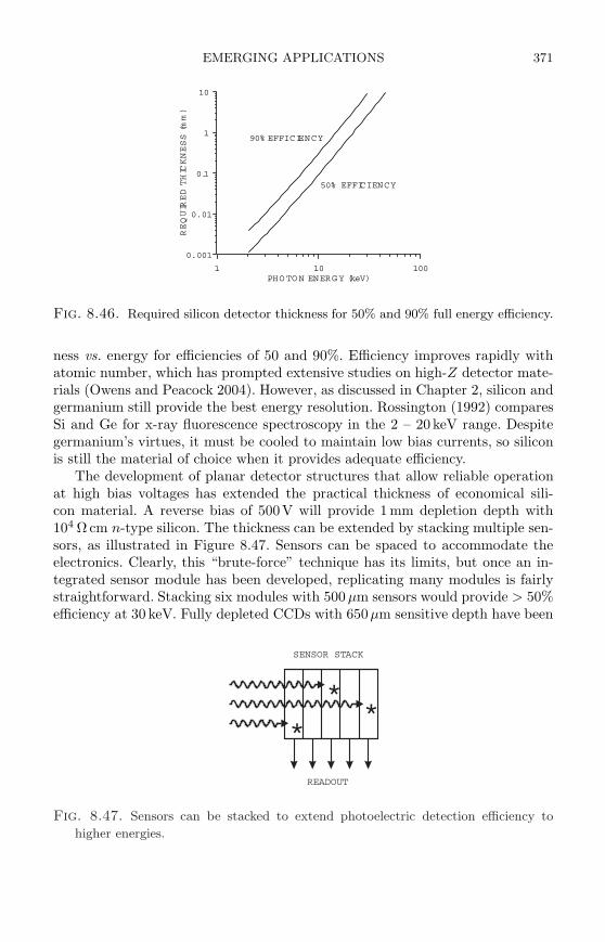
EMERGING APPLICATIONS 371
1 10 100PHOTON ENERGY (keV)
0.001
0.01
0.1
1
10
REQUIREDTHICKNESS(mm)
90% EFFICIENCY
50% EFFICIENCY
Fig. 8.46. Required silicon detector thickness for 50% and 90% full energy efficiency.
ness vs. energy for efficiencies of 50 and 90%. Efficiency improves rapidly withatomic number, which has prompted extensive studies on high-Z detector mate-rials (Owens and Peacock 2004). However, as discussed in Chapter 2, silicon andgermanium still provide the best energy resolution. Rossington (1992) comparesSi and Ge for x-ray fluorescence spectroscopy in the 2 – 20 keV range. Despitegermanium’s virtues, it must be cooled to maintain low bias currents, so siliconis still the material of choice when it provides adequate efficiency.
The development of planar detector structures that allow reliable operationat high bias voltages has extended the practical thickness of economical sili-con material. A reverse bias of 500V will provide 1 mm depletion depth with104 Ω cm n-type silicon. The thickness can be extended by stacking multiple sen-sors, as illustrated in Figure 8.47. Sensors can be spaced to accommodate theelectronics. Clearly, this “brute-force” technique has its limits, but once an in-tegrated sensor module has been developed, replicating many modules is fairlystraightforward. Stacking six modules with 500µm sensors would provide > 50%efficiency at 30 keV. Fully depleted CCDs with 650µm sensitive depth have been
*
**
READOUT
SENSOR STACK
Fig. 8.47. Sensors can be stacked to extend photoelectric detection efficiency to
higher energies.
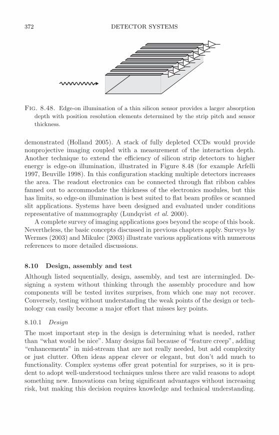
372 DETECTOR SYSTEMS
Fig. 8.48. Edge-on illumination of a thin silicon sensor provides a larger absorption
depth with position resolution elements determined by the strip pitch and sensor
thickness.
demonstrated (Holland 2005). A stack of fully depleted CCDs would providenonprojective imaging coupled with a measurement of the interaction depth.Another technique to extend the efficiency of silicon strip detectors to higherenergy is edge-on illumination, illustrated in Figure 8.48 (for example Arfelli1997, Beuville 1998). In this configuration stacking multiple detectors increasesthe area. The readout electronics can be connected through flat ribbon cablesfanned out to accommodate the thickness of the electronics modules, but thishas limits, so edge-on illumination is best suited to flat beam profiles or scannedslit applications. Systems have been designed and evaluated under conditionsrepresentative of mammography (Lundqvist et al. 2000).
A complete survey of imaging applications goes beyond the scope of this book.Nevertheless, the basic concepts discussed in previous chapters apply. Surveys byWermes (2003) and Mikulec (2003) illustrate various applications with numerousreferences to more detailed discussions.
8.10 Design, assembly and test
Although listed sequentially, design, assembly, and test are intermingled. De-signing a system without thinking through the assembly procedure and howcomponents will be tested invites surprises, from which one may not recover.Conversely, testing without understanding the weak points of the design or tech-nology can easily become a major effort that misses key points.
8.10.1 Design
The most important step in the design is determining what is needed, ratherthan “what would be nice”. Many designs fail because of “feature creep”, adding“enhancements” in mid-stream that are not really needed, but add complexityor just clutter. Often ideas appear clever or elegant, but don’t add much tofunctionality. Complex systems offer great potential for surprises, so it is pru-dent to adopt well-understood techniques unless there are valid reasons to adoptsomething new. Innovations can bring significant advantages without increasingrisk, but making this decision requires knowledge and technical understanding.

DESIGN, ASSEMBLY AND TEST 373
Superficial judgments can kill innovations that are good or accept innovationsthat lead to grief. A little bit of knowledge can be a bad thing.
Sensor technology is very well developed. For applications that don’t requirethe utmost in radiation resistance, silicon sensors are available from several ven-dors without requiring extensive development programs. Again, the most impor-tant point is determining what is really needed.
IC design commonly is a problem area. On the one hand, the availability of“free” design software and inexpensive access to multiproject fabrication runs al-lows just about anyone to design an IC and obtain some chips. Some groups haveused this approach very effectively, but many have failed. Designing a successfulIC requires more than expertise in circuit design. Since these are special purposeICs, the application environment is not as well understood as for mainstreamdevices. Furthermore, the ICs of interest in this context tend to be rather com-plex subsystems, which in turn must be integrated into a system. This requiresmore breadth than found in typical university engineering departments, whichtend to emphasize specialization.
The other side of the IC design problem occurs in groups of professionals.Highly sophisticated design tools assist in cycles of
1. establishing an initial design,
2. simulating its electrical performance,
3. laying out the silicon IC,
4. extracting parasitic resistances, capacitances, and inductances,
5. incorporating parasitics into the circuit simulation,
6. revising the design,
7. another cycle?
Simulations are performed at the circuit level, block level, and for the completeIC. They must evaluate performance over the range of parameter variationsspecified for the IC fabrication process (“corner parameters”). MOSFET modelsin the weak and moderate inversion regime often show significant disagreementwith measured device data, so models should be checked against test devices.Output resistance is another problem area. Often different simulators claimingthe same functionality will find (or miss) different problems, so multiple simulatorruns are necessary. On a complex IC this can be quite time consuming. Afterthe design and layout was completed, the presubmission simulations and designverifications of the ATLAS pixel IC took several months, but when received theIC performed to design specifications. Unfortunately, the better simulation andverification packages are expensive.
A common pitfall is the last minute change that is deemed so simple that anew verification is not necessary. Deadlines often lead to premature submissions.Schedules are necessary to keep a project on track, but the time lost by sub-mitting and then troubleshooting a flawed design is much greater than delayingsubmission to complete the full suite of verifications.
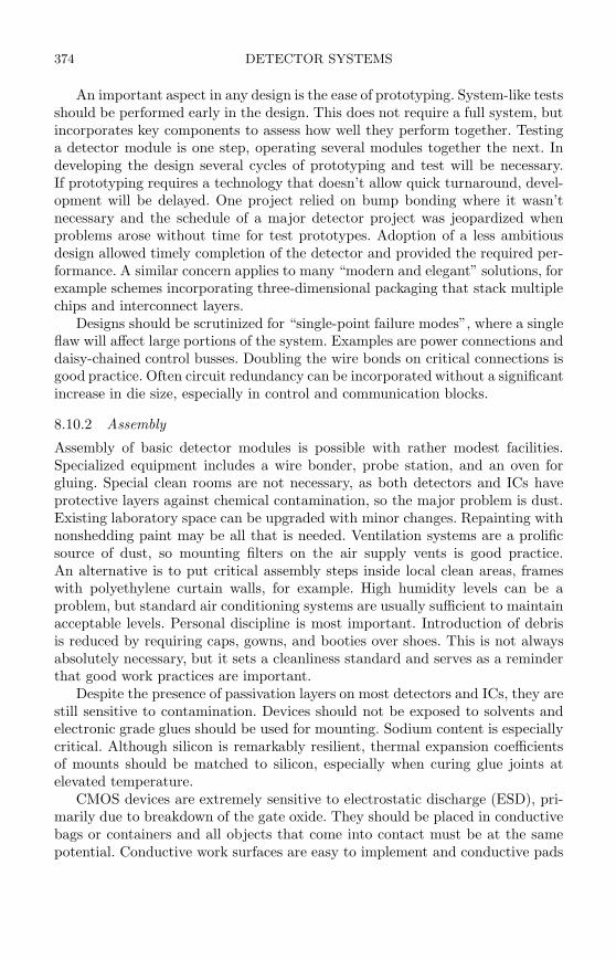
374 DETECTOR SYSTEMS
An important aspect in any design is the ease of prototyping. System-like testsshould be performed early in the design. This does not require a full system, butincorporates key components to assess how well they perform together. Testinga detector module is one step, operating several modules together the next. Indeveloping the design several cycles of prototyping and test will be necessary.If prototyping requires a technology that doesn’t allow quick turnaround, devel-opment will be delayed. One project relied on bump bonding where it wasn’tnecessary and the schedule of a major detector project was jeopardized whenproblems arose without time for test prototypes. Adoption of a less ambitiousdesign allowed timely completion of the detector and provided the required per-formance. A similar concern applies to many “modern and elegant” solutions, forexample schemes incorporating three-dimensional packaging that stack multiplechips and interconnect layers.
Designs should be scrutinized for “single-point failure modes”, where a singleflaw will affect large portions of the system. Examples are power connections anddaisy-chained control busses. Doubling the wire bonds on critical connections isgood practice. Often circuit redundancy can be incorporated without a significantincrease in die size, especially in control and communication blocks.
8.10.2 Assembly
Assembly of basic detector modules is possible with rather modest facilities.Specialized equipment includes a wire bonder, probe station, and an oven forgluing. Special clean rooms are not necessary, as both detectors and ICs haveprotective layers against chemical contamination, so the major problem is dust.Existing laboratory space can be upgraded with minor changes. Repainting withnonshedding paint may be all that is needed. Ventilation systems are a prolificsource of dust, so mounting filters on the air supply vents is good practice.An alternative is to put critical assembly steps inside local clean areas, frameswith polyethylene curtain walls, for example. High humidity levels can be aproblem, but standard air conditioning systems are usually sufficient to maintainacceptable levels. Personal discipline is most important. Introduction of debrisis reduced by requiring caps, gowns, and booties over shoes. This is not alwaysabsolutely necessary, but it sets a cleanliness standard and serves as a reminderthat good work practices are important.
Despite the presence of passivation layers on most detectors and ICs, they arestill sensitive to contamination. Devices should not be exposed to solvents andelectronic grade glues should be used for mounting. Sodium content is especiallycritical. Although silicon is remarkably resilient, thermal expansion coefficientsof mounts should be matched to silicon, especially when curing glue joints atelevated temperature.
CMOS devices are extremely sensitive to electrostatic discharge (ESD), pri-marily due to breakdown of the gate oxide. They should be placed in conductivebags or containers and all objects that come into contact must be at the samepotential. Conductive work surfaces are easy to implement and conductive pads
DESIGN, ASSEMBLY AND TEST 375
can be placed on the floor. Conductivity need not be high; even wood or card-board typically absorb enough moisture to drain off charge, although one shouldnot rely on that. Plastic work surfaces and garments of synthetic fabrics shouldbe avoided. Assembly staff commonly wear wrist straps, but they must be con-nected to an appropriate reference point. Severe ESD creates small “craters”on the device and is easy to diagnose, but even without causing breakdown thedamage to the gate oxide affects device characteristics. One widely reported caseof “mysterious” IC failures nearly led to a requirement for retesting ICs at ev-ery handling step. Asking the people who actually did the work provided theexplanation – ESD due to poor handling procedures. Unnecessary retesting ofdice and detector wafers should be avoided, as they are most vulnerable beforemounting.
Large-scale systems are more demanding than small prototype runs, as re-covering from failures requires more time and effort. Production assembly occursat many levels and can be distributed efficiently across multiple institutions, asit often must because of multiple funding sources. Specialized tooling must bedeveloped and maintained and metrology systems are essential to check andmaintain mechanical precision. This does require temperature control and forthe assembly of large systems specially prepared spaces are essential.
8.10.3 Testing
Testing means many things to many people. Incomplete testing is common, fromthe practitioner’s “I switched it on and it works” to the IC engineer who afterdetailed measurements proclaims a chip to be “fully functional”, although it isunusable because it doesn’t work in a system. Tests must have specified goalsand the reach of the test must be well-understood. To avoid unnecessary de-lays, test strategies and techniques must be developed during the design phase(they usually aren’t). The functional requirements of detector readout ICs oftenprovide built-in test capabilities. For example, on-chip charge injection circuitryprovides a test of analog performance at the wafer probe level and appropriatecommand sets can be developed that exercise digital functions. Preparing a testsystem requires time, so it is wise not to wait until the chips arrive (althoughthat’s what usually happens).
Although we all like to plan for success, testing should anticipate failure.Testing detectors and ICs prior to combining them in a detector module makesit easier to localize problems. Detector yields can be quite high, but with IC yieldsranging from 20 to 90% testing is essential. Probe stations can be equipped withprobe cards that allow contacting many pads at once (64 or 128 probes arecommon). Semi-automatic probe stations will step from die to die on a waferand automated measurement systems can record test conditions and measuredresults for future reference (see Anghinolfi et al. 2002, for example). Identifyingyield-critical fabrication steps is very important. For example, chip failures onassembled modules require delicate rework, which can easily cause new problems,so screening of individual ICs prior to assembly must be thorough to ensure a
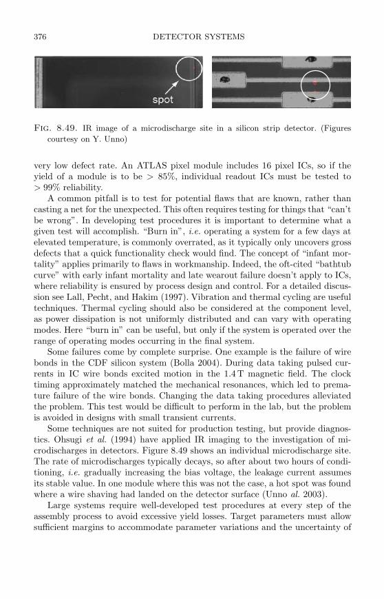
376 DETECTOR SYSTEMS
Fig. 8.49. IR image of a microdischarge site in a silicon strip detector. (Figures
courtesy on Y. Unno)
very low defect rate. An ATLAS pixel module includes 16 pixel ICs, so if theyield of a module is to be > 85%, individual readout ICs must be tested to> 99% reliability.
A common pitfall is to test for potential flaws that are known, rather thancasting a net for the unexpected. This often requires testing for things that “can’tbe wrong”. In developing test procedures it is important to determine what agiven test will accomplish. “Burn in”, i.e. operating a system for a few days atelevated temperature, is commonly overrated, as it typically only uncovers grossdefects that a quick functionality check would find. The concept of “infant mor-tality” applies primarily to flaws in workmanship. Indeed, the oft-cited “bathtubcurve” with early infant mortality and late wearout failure doesn’t apply to ICs,where reliability is ensured by process design and control. For a detailed discus-sion see Lall, Pecht, and Hakim (1997). Vibration and thermal cycling are usefultechniques. Thermal cycling should also be considered at the component level,as power dissipation is not uniformly distributed and can vary with operatingmodes. Here “burn in” can be useful, but only if the system is operated over therange of operating modes occurring in the final system.
Some failures come by complete surprise. One example is the failure of wirebonds in the CDF silicon system (Bolla 2004). During data taking pulsed cur-rents in IC wire bonds excited motion in the 1.4 T magnetic field. The clocktiming approximately matched the mechanical resonances, which led to prema-ture failure of the wire bonds. Changing the data taking procedures alleviatedthe problem. This test would be difficult to perform in the lab, but the problemis avoided in designs with small transient currents.
Some techniques are not suited for production testing, but provide diagnos-tics. Ohsugi et al. (1994) have applied IR imaging to the investigation of mi-crodischarges in detectors. Figure 8.49 shows an individual microdischarge site.The rate of microdischarges typically decays, so after about two hours of condi-tioning, i.e. gradually increasing the bias voltage, the leakage current assumesits stable value. In one module where this was not the case, a hot spot was foundwhere a wire shaving had landed on the detector surface (Unno al. 2003).
Large systems require well-developed test procedures at every step of theassembly process to avoid excessive yield losses. Target parameters must allowsufficient margins to accommodate parameter variations and the uncertainty of
SUMMARY 377
radiation load estimates. Component screening is typically conducted at roomtemperature, whereas some systems must operate cold, so the temperature de-pendence of operating parameters must also be accounted for. ATLAS and CMShave both developed detailed assembly and test procedures with extensive datatracking of individual components. Since practically all major steps are dis-tributed over multiple institutions, performance specifications must be monitoredand enforced at multiple sites. This allows some latitude in the choice of equip-ment and both experiments appear to have dealt successfully with fabricationprocesses that span the globe.
8.11 Summary
High energy physics experiments have driven the technology of large-scale semi-conductor detector systems and we can expect this to continue. Although notcomprehensive, the examples shown above illustrate the diversity of implemen-tations. Since the overall utility of a complex system accrues from many com-ponents, there is no single “correct” design. Use of a mature and well-developedtechnology provides flexibility in choosing implementations and usually allows“work arounds” to solve unanticipated problems. The choice of technology de-pends on access to expertise. For example, the success of the flex hybrids usedin the ATLAS SCT was critically dependent on access to an experienced andreliable vendor willing to take on a rather small project. Although the choice oftechnology is important, thorough design and implementation are crucial. Sometechnologies are only available commercially for large volume orders, so theyare impractical for small-scale R&D and could severely impede the design andprototyping effort in larger systems.
Silicon strip technology is quite mature. Nevertheless, as in the past, it ap-pears that acceptable radiation limits are set by the sensor, rather than theelectronics, so improvements in sensor technology will increase radiation resis-tance. As the size of silicon trackers increases, technologies for signal and powerbussing as for cooling and support systems will gain increased importance. Re-duced feature sizes in ICs raise the same issue. Device performance dependson current, but operating voltages are dropping with feature size. Power buss-ing is becoming much more critical, as voltage drops must be controlled moretightly. The ability to supply power at elevated voltage and reduced current willbecome more important in controlling both voltage drops and material, but effi-cient power conversion techniques must be developed that will function in highmagnetic fields and sustain radiation damage.
Pixel systems remain the frontier. CCD technology now offers larger sensi-tive depths in fully depleted devices, which extends x-ray detection to higherenergies and increases the signal in particle tracking. The increased signal main-tains signal-to-noise ratio at higher readout rates. Overall frame rates can beincreased by adopting column-parallel readout. DEPFET arrays offer similarcharacteristics and performance, with the additional feature of selective read-
378 DETECTOR SYSTEMS
out. The fabrication facilities used for both CCDs and DEPFETs can provide“wafer-scale” devices and are geared to special requirements.
Active pixel sensors utilizing mainstream CMOS foundry processes offer theimportant benefits of mechanical simplicity and access to fabrication. High-density circuitry is possible, so that the complexity of readout cells can go beyondthe simple readout matrices used in digital cameras. However, the signal origi-nates in an ancillary component of the process, the doping and thickness of theepitaxial layer, so industry trends are not well aligned with the requirementsof detectors. As these devices are limited to standard IC die sizes, tiling is animportant design consideration in large arrays. The devices can be thinned toreduce material, but this must be balanced against the required support struc-tures together with the signal and power bussing. Although limited in designflexibility, this technology offers significant benefits in those applications thatcan find an acceptable compromise in performance.
The hybrid pixel array, which combines separate sensor and readout units,has many advantages. It opens up the choice of sensor material, be it for x-raydetection or increased radiation resistance, and the readout can exploit futureadvances in IC technology. Tiling in large arrays is facilitated, as the sensor can“bridge” the gaps between the readout ICs. Gaps between arrays can be reducedby advanced sensor designs, for example “3D sensors” that can practically elim-inate inactive edge regions. The drawback of the hybrid array is the complexityof bump bonding. Industry is moving towards smaller bonding pitches (John etal. 2004), so this situation could change and the technology should become moreaccessible as high-density packaging in the electronics industry proliferates.
References
Abbaneo, D. (2004). Layout and performance of the CMS Silicon Strip Tracker.Nucl. Instr. and Meth. A518 (2004) 331–335
Abe, K. et al. (1997). Design and performance of the SLD vertex detector: a307 Mpixel tracking system. Nucl. Instr. and Meth. A400 (1997) 287–343
Adolphsen, C. et al. (1992). The Mark-II silicon strip vertex detector. Nucl.Instr. and Meth. A313 (1992) 63–10
Albiol, F. et al. (1998). Performance of the ATLAS silicon strip detector mod-ules. Nucl. Instr. and Meth. A403 (1998) 247–255
Allport, P.P. et al. (1994). The OPAL silicon strip microvertex detector withtwo coordinate readout. Nucl. Instr. and Meth. A346 (1994) 476–495
Alpat, B. et al. (1992). The design of the L3 silicon microvertex detector. Nucl.Instr. and Meth. A315 (1992) 197–200
Anghinolfi, F. et al. (2002). ASIC wafer test system for the ATLAS Semicon-ductor Tracker front-end chip. IEEE Trans. Nucl. Sci. 49/3 (2002) 1080–1085
ATLAS TDR (1997). ATLAS Inner Detector Technical Design Report.CERN/LHCC/97-16 and 97-17. ISBN 92-9083-102-2 and 92-9083-103-0.available at http://atlas.web.cern.ch/Atlas/internal/tdr.html
REFERENCES 379
Attwood, W.B. (1994). Gamma Large Area Silicon Telescope (GLAST) – ap-plying silicon strip technology to the detection of gamma rays in space. Nucl.Instr. and Meth. A342 (1994) 302–307
Barbero, M. et al. (2004). Design and test of the CMS pixel readout chip. Nucl.Instr. and Meth. A517 (2004) 349–359
Barkan, O. et al. (1991). Development of a customized SSC pixel detectorreadout for vertex tracking. Proceedings of the Symposium on Detector Re-search and Development for the Superconducting Super Collider, October 15–18, 1990. eds T. Dombeck, V. Kelley, G. Yost, World Scientific, Singapore
Batignani, G. et al. (1993). Operational experience with a large detector systemusing silicon strip detectors with double sided readout. Nucl. Instrum. andMeth. A326 (1993) 183–188
Battaligia, M. (2004). The Vertex Tracker at future e+e− linear colliders. Nucl.Instr. and Meth. A530 (2004) 33–37
Bean, A. (2001). Status of the D∅ Silicon Microstrip Tracker. Nucl. Instr. andMeth. A466 (2001) 262–267
Bebek, C.J. et al. (2002). Proton radiation damage in high-resistivity n-typesilicon CCDs. SPIE 4669 (2002) 161–171 and LBNL-49316
Becks, K.H. et al. (1997). The DELPHI pixels. Nucl. Instr. and Meth. A386(1997) 11–17
Bellazini, R. et al. (2003). The silicon-strip tracker of the Gamma ray LargeArea Space Telescope. Nucl. Instr. and Meth. A512 (2003) 136–142
Bergauer, T. (2004). Tests of the silicon strip sensors for the CMS tracker. Nucl.Instr. and Meth. A518 (2004) 317–320
Biasini, M. (2004). The construction of the Silicon Strip Tracker for the CMSexperiment. Nucl. Instr. and Meth. A530 (2004) 17–22
Bingefors, N. et al. (1993). A novel technique for fast pulse shaping using a slowamplifier at LHC. Nucl. Instr. and Meth. A326 (1993) 112–119
Blanquart, L. et al. (2004). FE-I2: A front-end readout chip designed in a com-mercial 0.25 µm process for the ATLAS pixel detector at LHC. IEEE Trans.Nucl. Sci. NS-51/4 (2004) 1358–1364
Braibant, S. et al. (2002). Investigation of design parameters for radiation hardsilicon microstrip detectors. Nucl. Instr. and Meth. A485 (2002) 343–361
Brau, J.E. and Sinev, N. (2000). Operation of a CCD particle detector in thepresence of bulk neutron damage. IEEE Trans. Nucl. Sci 47/6 (2000) 1898–1901
Brau, J.E. et al. (2004). Investigation of radiation damage in the SLD CCDvertex detector. IEEE Trans. Nucl. Sci 51/4 (2004) 1742–1746
Campabadal, F. et al. (2005a). Design and performance of the ABCD3TA ASICfor readout of silicon strip detectors in the ATLAS Semiconductor Tracker.Nucl. Instr. and Meth., to be published
Campabadal, F. et al. (2005b). Beam tests of ATLAS SCT silicon strip detectormodules. Nucl. Instr. and Meth. A538 (2005) 384–407
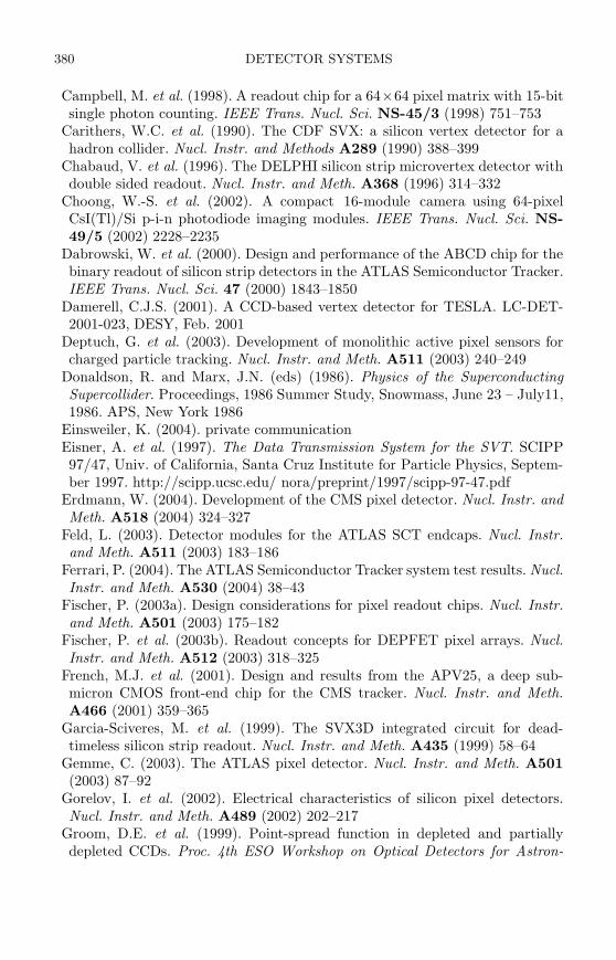
380 DETECTOR SYSTEMS
Campbell, M. et al. (1998). A readout chip for a 64×64 pixel matrix with 15-bitsingle photon counting. IEEE Trans. Nucl. Sci. NS-45/3 (1998) 751–753
Carithers, W.C. et al. (1990). The CDF SVX: a silicon vertex detector for ahadron collider. Nucl. Instr. and Methods A289 (1990) 388–399
Chabaud, V. et al. (1996). The DELPHI silicon strip microvertex detector withdouble sided readout. Nucl. Instr. and Meth. A368 (1996) 314–332
Choong, W.-S. et al. (2002). A compact 16-module camera using 64-pixelCsI(Tl)/Si p-i-n photodiode imaging modules. IEEE Trans. Nucl. Sci. NS-49/5 (2002) 2228–2235
Dabrowski, W. et al. (2000). Design and performance of the ABCD chip for thebinary readout of silicon strip detectors in the ATLAS Semiconductor Tracker.IEEE Trans. Nucl. Sci. 47 (2000) 1843–1850
Damerell, C.J.S. (2001). A CCD-based vertex detector for TESLA. LC-DET-2001-023, DESY, Feb. 2001
Deptuch, G. et al. (2003). Development of monolithic active pixel sensors forcharged particle tracking. Nucl. Instr. and Meth. A511 (2003) 240–249
Donaldson, R. and Marx, J.N. (eds) (1986). Physics of the SuperconductingSupercollider. Proceedings, 1986 Summer Study, Snowmass, June 23 – July11,1986. APS, New York 1986
Einsweiler, K. (2004). private communicationEisner, A. et al. (1997). The Data Transmission System for the SVT. SCIPP97/47, Univ. of California, Santa Cruz Institute for Particle Physics, Septem-ber 1997. http://scipp.ucsc.edu/ nora/preprint/1997/scipp-97-47.pdf
Erdmann, W. (2004). Development of the CMS pixel detector. Nucl. Instr. andMeth. A518 (2004) 324–327
Feld, L. (2003). Detector modules for the ATLAS SCT endcaps. Nucl. Instr.and Meth. A511 (2003) 183–186
Ferrari, P. (2004). The ATLAS Semiconductor Tracker system test results. Nucl.Instr. and Meth. A530 (2004) 38–43
Fischer, P. (2003a). Design considerations for pixel readout chips. Nucl. Instr.and Meth. A501 (2003) 175–182
Fischer, P. et al. (2003b). Readout concepts for DEPFET pixel arrays. Nucl.Instr. and Meth. A512 (2003) 318–325
French, M.J. et al. (2001). Design and results from the APV25, a deep sub-micron CMOS front-end chip for the CMS tracker. Nucl. Instr. and Meth.A466 (2001) 359–365
Garcia-Sciveres, M. et al. (1999). The SVX3D integrated circuit for dead-timeless silicon strip readout. Nucl. Instr. and Meth. A435 (1999) 58–64
Gemme, C. (2003). The ATLAS pixel detector. Nucl. Instr. and Meth. A501(2003) 87–92
Gorelov, I. et al. (2002). Electrical characteristics of silicon pixel detectors.Nucl. Instr. and Meth. A489 (2002) 202–217
Groom, D.E. et al. (1999). Point-spread function in depleted and partiallydepleted CCDs. Proc. 4th ESO Workshop on Optical Detectors for Astron-
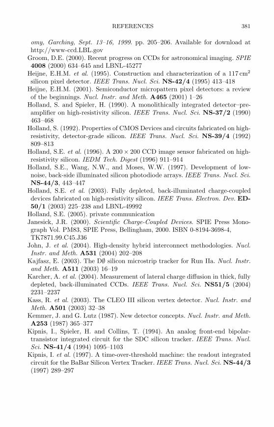
REFERENCES 381
omy, Garching, Sept. 13–16, 1999. pp. 205–206. Available for download athttp://www-ccd.LBL.gov
Groom, D.E. (2000). Recent progress on CCDs for astronomical imaging. SPIE4008 (2000) 634–645 and LBNL-45277
Heijne, E.H.M. et al. (1995). Construction and characterization of a 117 cm2
silicon pixel detector. IEEE Trans. Nucl. Sci. NS-42/4 (1995) 413–418Heijne, E.H.M. (2001). Semiconductor micropattern pixel detectors: a reviewof the beginnings. Nucl. Instr. and Meth. A465 (2001) 1–26
Holland, S. and Spieler, H. (1990). A monolithically integrated detector–pre-amplifier on high-resistivity silicon. IEEE Trans. Nucl. Sci. NS-37/2 (1990)463–468
Holland, S. (1992). Properties of CMOS Devices and circuits fabricated on high-resistivity, detector-grade silicon. IEEE Trans. Nucl. Sci. NS-39/4 (1992)809–813
Holland, S.E. et al. (1996). A 200× 200 CCD image sensor fabricated on high-resistivity silicon. IEDM Tech. Digest (1996) 911–914
Holland, S.E., Wang, N.W., and Moses, W.W. (1997). Development of low-noise, back-side illuminated silicon photodiode arrays. IEEE Trans. Nucl. Sci.NS-44/3, 443–447
Holland, S.E. et al. (2003). Fully depleted, back-illuminated charge-coupleddevices fabricated on high-resistivity silicon. IEEE Trans. Electron. Dev. ED-50/1 (2003) 225–238 and LBNL-49992
Holland, S.E. (2005). private communicationJanesick, J.R. (2000). Scientific Charge-Coupled Devices. SPIE Press Mono-graph Vol. PM83, SPIE Press, Bellingham, 2000. ISBN 0-8194-3698-4,TK7871.99.C45.J36
John, J. et al. (2004). High-density hybrid interconnect methodologies. Nucl.Instr. and Meth. A531 (2004) 202–208
Kajfasz, E. (2003). The D∅ silicon microstrip tracker for Run IIa. Nucl. Instr.and Meth. A511 (2003) 16–19
Karcher, A. et al. (2004). Measurement of lateral charge diffusion in thick, fullydepleted, back-illuminated CCDs. IEEE Trans. Nucl. Sci. NS51/5 (2004)2231–2237
Kass, R. et al. (2003). The CLEO III silicon vertex detector. Nucl. Instr. andMeth. A501 (2003) 32–38
Kemmer, J. and G. Lutz (1987). New detector concepts. Nucl. Instr. and Meth.A253 (1987) 365–377
Kipnis, I., Spieler, H. and Collins, T. (1994). An analog front-end bipolar-transistor integrated circuit for the SDC silicon tracker. IEEE Trans. Nucl.Sci. NS-41/4 (1994) 1095–1103
Kipnis, I. et al. (1997). A time-over-threshold machine: the readout integratedcircuit for the BaBar Silicon Vertex Tracker. IEEE Trans. Nucl. Sci. NS-44/3(1997) 289–297
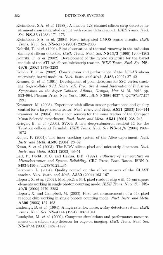
382 DETECTOR SYSTEMS
Kleinfelder, S.A. et al. (1988). A flexible 128 channel silicon strip detector in-strumentation integrated circuit with sparse data readout. IEEE Trans. Nucl.Sci. NS-35 (1988) 171–175
Kleinfelder, S.A. et al. (2004). Novel integrated CMOS sensor circuits. IEEETrans. Nucl. Sci. NS-51/5 (2004) 2328–2336
Kohriki, T. et al. (1996). First observation of thermal runaway in the radiationdamaged silicon detector. IEEE Trans. Nucl. Sci. NS43/3 (1996) 1200–1202
Kohriki, T. et al. (2002). Development of the hybrid structure for the barrelmodule of the ATLAS silicon-microstrip tracker. IEEE Trans. Nucl. Sci. NS-49/6 (2002) 1378–3283
Kondo, T. et al. (2002). Construction and performance of the ATLAS siliconmicrostrip barrel modules. Nucl. Instr. and Meth. A485 (2002) 27–42
Kramer, G. et al. (1991). Development of pixel detectors for SSC vertex track-ing. Supercollider 3 (J. Nonte, ed). Proc. 3rd Annual International IndustrialSymposium on the Super Collider, Atlanta, Georgia, Mar 13–15, 1991. pp.953–964. Plenum Press, New York, 1991. ISBN 0-3064-4037-7, QC787.P7.I571991
Krammer, M. (2003). Experience with silicon sensor performance and qualitycontrol for a large-area detector. Nucl. Instr. and Meth. A511 (2003) 136–144
Krammer, M. (2004). The silicon sensors for the inner tracker of the CompactMuon Solenoid experiment. Nucl. Instr. and Meth. A531 (2004) 238–245
Krieger, B. et al. (2004). SVX4: A new deep-submicron readout IC for theTevatron collider at Fermilab. IEEE Trans. Nucl. Sci. NS-51/5 (2004) 1968–1973
Kuijer, P. (2004). The inner tracking system of the Alice experiment. Nucl.Instr. and Meth. A530 (2004) 28–32
Kwan, S. et al. (2003). The BTeV silicon pixel and microstrip detectors. Nucl.Instr. and Meth. A511 (2003) 48–51
Lall, P., Pecht, M.G. and Hakim, E.B. (1997). Influence of Temperature onMicroelectronics and System Reliability. CRC Press, Boca Raton. ISBN 0-8493-9450-3, TK7870.25.L35
Latronico, L. (2004). Quality control on the silicon sensors of the GLASTtracker. Nucl. Instr. and Meth. A530 (2004) 163–167
Llopart, X. et al. (2002). Medipix2: a 64-k pixel readout chip with 55-µm squareelements working in single photon counting mode. IEEE Trans. Nucl. Sci. NS-49/5 (2002) 2279–2283
Llopart, X. and Campbell, M. (2003). First test measurements of a 64k pixelreadout chip working in single photon counting mode. Nucl. Instr. and Meth.A509 (2003) 157–163
Ludewigt, B. et al. (1994). A high rate, low noise, x-Ray detector system. IEEETrans. Nucl. Sci. NS-41/4 (1994) 1037–1041
Lundqvist, M. et al. (2000). Computer simulations and performance measure-ments on a silicon strip detector for edge-on imaging. IEEE Trans. Nucl. Sci.NS-47/4 (2000) 1487–1492
REFERENCES 383
Lynch, G. (1993). Figure 2.4 in Status Report on the Design of a Detector forthe Study of CP Violation at PEP-II at SLAC. SLAC-419, June, 1993
Macchiolo, A. (2004). Control of the fabrication process for the sensors of theCMS silicon tracker. Nucl. Instr. and Meth. A530 (2004) 54–58
Mandelli, E. et al. (2002). Digital column readout architecture for the ATLASpixel 0.25 µm front end IC. IEEE Trans. Nucl. Sci. NS-49/4 (2002) 1774–1777
Manfredi, P.F. et al. (1999). Functional characteristics and radiation toleranceof AToM, the front-end chip of BaBar Silicon Vertex Tracker. IEEE Trans.Nucl. Sci. NS-46/6 (1999) 1865–1870
Merkel, P. (2003). The CDF silicon detector upgrade and performance. Nucl.Instr. and Meth. A501 (2003) 1–6
Messenger, G.C. and Ash, M.S. (1986). The Effects of Radiation on ElectronicSystems. Van Nostrand Reinhold, New York. ISBN 0-442-25417-2,TK7870.M4425
Moorhead, G.F. (2002). Detector modules for the endcaps of the ATLAS semi-conductor tracker. Nucl. Instr. and Meth. A485 (2002) 43–53
Morselli, A. (2004). The GLAST tracker. Nucl. Instr. and Meth. A530 (2004)158–162
Nelson, D. (2004). Private communicationNisius, R. (2004). End-cap modules for the ATLAS SCT. Nucl. Instr. and Meth.A530 (2004) 44–49
Nyman, M. (1996). Private communicationOhsugi, T. et al. (1994). Microdischarges of AC-coupled silicon strip sensors.Nucl. Instr. and Meth. A342 (1994) 22–26
Ohsugi, T. et al. (1999). Design optimization of radiation-hard, double-sided,double-metal, AC-coupled silicon sensors. Nucl. Instr. and Meth. A436 (1999)272–280
Osterberg, K. (1999). Performance of the vertex detectors at LEP2. Nucl. Instr.and Meth. A435 (1999) 1–8
Owens, A. and A. Peacock (2004). Compound semiconductor radiation detec-tors Nucl. Instr. and Meth. A531 (2004) 18–37
Raymond, M. al. (2000). The CMS tracker APV25 0.25 µm CMOS readoutchip. 6th Workshop on Electronics for LHC Experiments, Krakow, September2000
RD48 (1999). 3rd RD48 Status Report (1999). CERN/LHCC 2000-0089.http://rd48.web.cern.ch/rd48/
Re, V. et al. (2003). Performance of the BaBar Silicon Vertex Tracker. Nucl.Instrum. and Meth. A501 (2003) 14–21
Richter, R.H. et al. (1996). Strip detector design for ATLAS and HERA-Busing two-dimensional device simulation. Nucl. Instr. and Meth. A377 (1996)412–421
Richter, R.H. et al. (2003). Design and technology of DEPFET pixel sensorsfor linear collider applications. Nucl. Instr. and Meth. A511 (2003) 250–256
384 DETECTOR SYSTEMS
Rossi, L. (2003). Pixel detectors hybridisation. Nucl. Instr. and Meth. A501(2003) 239–244
Schnetzer, S. (2003). The CMS pixel detector. Nucl. Instr. and Meth. A501(2003) 100–105
Schwarz, Andreas S. (1994a). Silicon strip vertex detectors at LEP. Nucl. Instr.and Meth. A342 (1994) 218–232
Schwarz, Andreas S. (1994b). Heavy flavor physics at colliders with silicon stripvertex detectors. Phys. Rept. 238 (1994) 1–133
Seiden, A. (1994). The SDC Silicon Tracker. IEEE Trans. Nucl. Sci. 41/4(1994) 779–784
Spieler, H. (1982). Unpublished note. The CCD output (ro ≈ 3 kΩ) drove anexternal common-gate JFET amplifier (gain ≈ 4) with an input impedanceof 100 Ω. A subsequent limiting amplifier (cascade of bipolar transistor dif-ferential pairs) constrained the amplitude of the clock pulse feedthrough andallowed retrieval of MIP level signals at a clock rate of 20MHz.
Spieler, H. (1994). Analog front-end electronics for the SDC Silicon Tracker,Nucl. Instr. and Meth. A342 (1994) 205–213
Spieler, H. (1988). Integrated microsystems as a driving force in modern detec-tor designs. in International Conference on the Impact of Digital Microelec-tronics and Microprocessors on Particle Physics. pp. 228–238. M. Budinich,E. Castelli, and A. Colavita (eds). World Scientific, Singapore. ISBN 9971-50-742-0
Stefanini, G. (2004). Progress in the ALICE silicon pixel detector. Nucl. Instr.and Meth. A530 (2004) 77–81
Stover, R.J. et al. (2004). Packaging design for Lawrence Berkeley NationalLaboratory high resistivity CCDs. SPIE 5499 58
Taylor, G. (2003). The Belle silicon vertex detector: present performance andupgrade plans. Nucl. Instr. and Meth. A501 (2003) 22–31
Turala, M. et al. (2001). The ATLAS semiconductor tracker. Nucl. Instr. andMeth. A466 (2001) 243–254
Turchetta, R. et al. (2003). Monolithic active pixel sensors (MAPS) in a VLSICMOS technology. Nucl. Instr. and Meth. A501 (2003) 251–259
Unno, Y. et al. (1996). Beam tests of a double-sided silicon strip detector withfast binary readout electronics before and after proton-irradiation. Nucl. Instr.and Meth. A383 (1996) 211–222
Unno, Y. et al. (2003). ATLAS silicon microstrip detector system (SCT). Nucl.Instr. and Meth. A511 (2003) 58–63
Ushiroda, Y. (2003). Belle silicon vertex detectors. Nucl. Instr. and Meth. A511(2003) 6–10
Weilhammer, P. (1994). Double-sided Si strip sensors for LEP vertex detectors.Nucl. Instr. and Meth. A342 (1994) 1–15
Wigmans, R. (2000). Calorimetry. Oxford University Press, Oxford. ISBN 0-19-850296-6
REFERENCES 385
Wunstorf, R. (2001). Radiation tolerant sensors for the ATLAS pixel detector.Nucl. Instr. and Meth. A466 (2001) 327–334
Yarema, R. et al. (1994). A Beginner’s Guide to the SVXII. Fermilab TM-1892, June, 1994. http://library.fnal.gov/archive/test-tm/1000/fermilab-tm-1892.pdf
Zimmerman, T. et al. (1995). The SVX2 readout chip. IEEE Trans. Nucl. Sci.NS-42/4 (1995) 803–807.
9
WHY THINGS DON’T WORK
After assembling a detector system a common experience is that it doesn’t workas expected. Apart from trivial problems such as disconnected cables, commonmaladies are spurious signals, self-oscillation, or excessive noise. This chapterdiscusses some common problems in detector systems and how to avoid them.
Throughout the previous lectures it was assumed that the only sources ofnoise were random, known, and in the detector, preamplifier, or associated com-ponents. In practice, the detector system will pick up spurious signals that arenot random, but not correlated with the signal, so with reference to the signalthey are quasi-random. These lead to baseline fluctuations superimposed on thedesired signal, which increase the detection threshold and degrade resolution.
It is important to distinguish between pickup of spurious signals, either fromlocal or remote sources (clock generators, digital circuitry, readout lines), andself-oscillation, where the system provides a feedback path that causes sustainedoscillation due to a portion of the output reaching the input. The same mecha-nisms that make a system sensitive to external pickup can also form a parasiticfeedback path.
This is not an exhaustive treatment; pickup mechanisms comprise a very com-plex system and just one weak area is sufficient to cause problems, so improvingone aspect will not always improve the situation, even if this improvement isessential. Texts with more details are listed in the bibliography at the end of thischapter.
9.1 Reflections on transmission lines
Signals are transmitted from one unit to another through transmission lines, of-ten coaxial cables or ribbon cables. When transmission lines are not terminatedwith their characteristic impedance, the signals are reflected. As a signal prop-agates along the cable, the ratio of instantaneous voltage to current equals thecable’s characteristic impedance Z0 =
√
L/C, where L and C are the induc-tance and capacitance per unit length. Typical impedances are 50 or 75 Ω forcoaxial cables and ∼ 100 Ω for ribbon cables. If at the receiving end the cable isconnected to a resistance different from the cable impedance, a different ratio ofvoltage to current must be established. This occurs through a reflected signal.If the termination is less than the line impedance, the voltage must be smallerand the reflected voltage wave has the opposite sign. If the termination is greaterthan the line impedance, the voltage wave is reflected with the same polarity.Conversely, the current in the reflected wave is of like sign when the termina-tion is less than the line impedance and of opposite sign when the termination
386
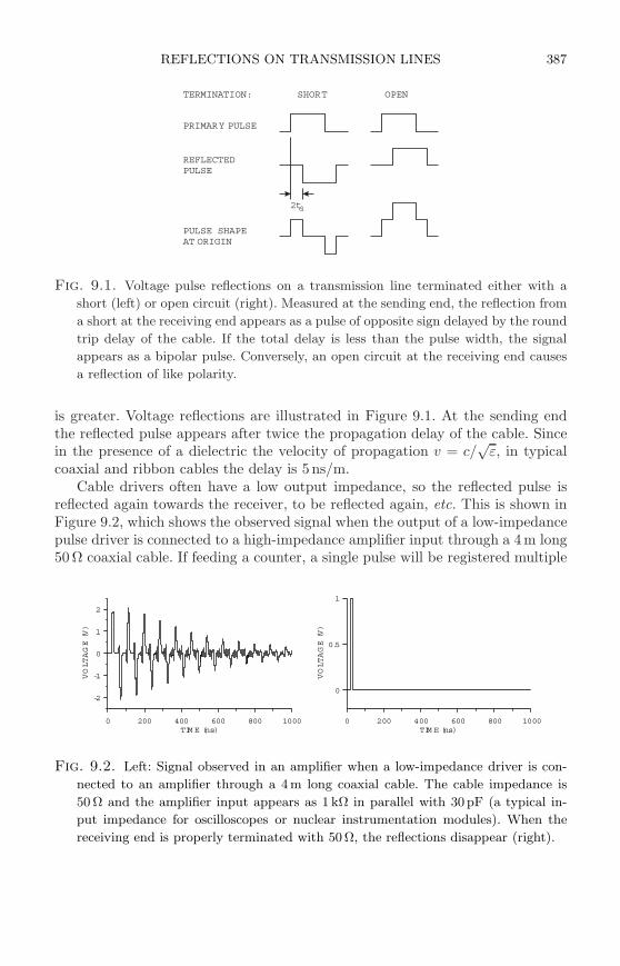
REFLECTIONS ON TRANSMISSION LINES 387
2td
TERMINATION: SHORT OPEN
REFLECTEDPULSE
PRIMARY PULSE
PULSE SHAPEAT ORIGIN
Fig. 9.1. Voltage pulse reflections on a transmission line terminated either with a
short (left) or open circuit (right). Measured at the sending end, the reflection from
a short at the receiving end appears as a pulse of opposite sign delayed by the round
trip delay of the cable. If the total delay is less than the pulse width, the signal
appears as a bipolar pulse. Conversely, an open circuit at the receiving end causes
a reflection of like polarity.
is greater. Voltage reflections are illustrated in Figure 9.1. At the sending endthe reflected pulse appears after twice the propagation delay of the cable. Sincein the presence of a dielectric the velocity of propagation v = c/
√ε, in typical
coaxial and ribbon cables the delay is 5 ns/m.Cable drivers often have a low output impedance, so the reflected pulse is
reflected again towards the receiver, to be reflected again, etc. This is shown inFigure 9.2, which shows the observed signal when the output of a low-impedancepulse driver is connected to a high-impedance amplifier input through a 4m long50 Ω coaxial cable. If feeding a counter, a single pulse will be registered multiple
0 200 400 600 800 1000TIM E (ns)
-2
-1
0
1
2
VOLTAGE(V)
0 200 400 600 800 1000TIM E (ns)
0
0.5
1
VOLTAGE(V)
Fig. 9.2. Left: Signal observed in an amplifier when a low-impedance driver is con-
nected to an amplifier through a 4 m long coaxial cable. The cable impedance is
50 Ω and the amplifier input appears as 1 kΩ in parallel with 30 pF (a typical in-
put impedance for oscilloscopes or nuclear instrumentation modules). When the
receiving end is properly terminated with 50 Ω, the reflections disappear (right).
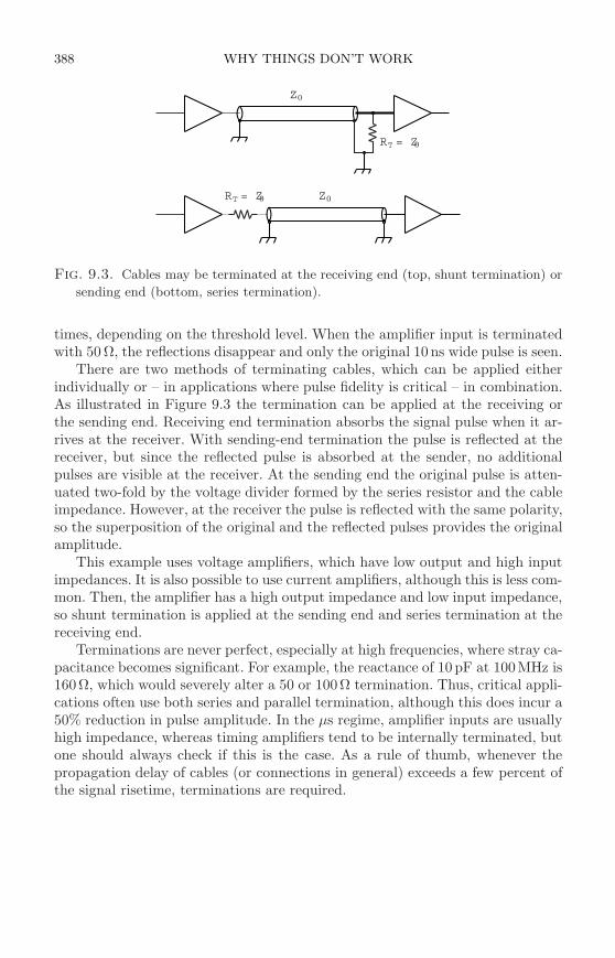
388 WHY THINGS DON’T WORK
Z
Z
R
R
= Z
= Z
0
0
T
T
0
0
Fig. 9.3. Cables may be terminated at the receiving end (top, shunt termination) or
sending end (bottom, series termination).
times, depending on the threshold level. When the amplifier input is terminatedwith 50 Ω, the reflections disappear and only the original 10 ns wide pulse is seen.
There are two methods of terminating cables, which can be applied eitherindividually or – in applications where pulse fidelity is critical – in combination.As illustrated in Figure 9.3 the termination can be applied at the receiving orthe sending end. Receiving end termination absorbs the signal pulse when it ar-rives at the receiver. With sending-end termination the pulse is reflected at thereceiver, but since the reflected pulse is absorbed at the sender, no additionalpulses are visible at the receiver. At the sending end the original pulse is atten-uated two-fold by the voltage divider formed by the series resistor and the cableimpedance. However, at the receiver the pulse is reflected with the same polarity,so the superposition of the original and the reflected pulses provides the originalamplitude.
This example uses voltage amplifiers, which have low output and high inputimpedances. It is also possible to use current amplifiers, although this is less com-mon. Then, the amplifier has a high output impedance and low input impedance,so shunt termination is applied at the sending end and series termination at thereceiving end.
Terminations are never perfect, especially at high frequencies, where stray ca-pacitance becomes significant. For example, the reactance of 10 pF at 100MHz is160Ω, which would severely alter a 50 or 100Ω termination. Thus, critical appli-cations often use both series and parallel termination, although this does incur a50% reduction in pulse amplitude. In the µs regime, amplifier inputs are usuallyhigh impedance, whereas timing amplifiers tend to be internally terminated, butone should always check if this is the case. As a rule of thumb, whenever thepropagation delay of cables (or connections in general) exceeds a few percent ofthe signal risetime, terminations are required.
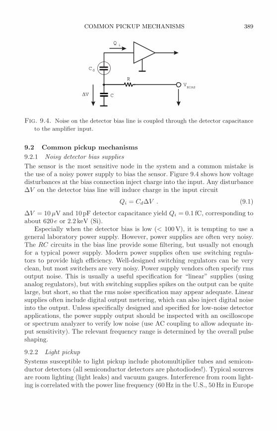
COMMON PICKUP MECHANISMS 389
C
Q
V
d
i
BIAS
V C
R
Fig. 9.4. Noise on the detector bias line is coupled through the detector capacitance
to the amplifier input.
9.2 Common pickup mechanisms
9.2.1 Noisy detector bias supplies
The sensor is the most sensitive node in the system and a common mistake isthe use of a noisy power supply to bias the sensor. Figure 9.4 shows how voltagedisturbances at the bias connection inject charge into the input. Any disturbance∆V on the detector bias line will induce charge in the input circuit
Qi = Cd∆V . (9.1)
∆V = 10 µV and 10pF detector capacitance yield Qi = 0.1 fC, corresponding toabout 620 e or 2.2 keV (Si).
Especially when the detector bias is low (< 100V), it is tempting to use ageneral laboratory power supply. However, power supplies are often very noisy.The RC circuits in the bias line provide some filtering, but usually not enoughfor a typical power supply. Modern power supplies often use switching regula-tors to provide high efficiency. Well-designed switching regulators can be veryclean, but most switchers are very noisy. Power supply vendors often specify rmsoutput noise. This is usually a useful specification for “linear” supplies (usinganalog regulators), but with switching supplies spikes on the output can be quitelarge, but short, so that the rms noise specification may appear adequate. Linearsupplies often include digital output metering, which can also inject digital noiseinto the output. Unless specifically designed and specified for low-noise detectorapplications, the power supply output should be inspected with an oscilloscopeor spectrum analyzer to verify low noise (use AC coupling to allow adequate in-put sensitivity). The relevant frequency range is determined by the overall pulseshaping.
9.2.2 Light pickup
Systems susceptible to light pickup include photomultiplier tubes and semicon-ductor detectors (all semiconductor detectors are photodiodes!). Typical sourcesare room lighting (light leaks) and vacuum gauges. Interference from room light-ing is correlated with the power line frequency (60Hz in the U.S., 50Hz in Europe

390 WHY THINGS DON’T WORK
Q
Vb
C+ C t ( )
DETECTOR SHIELD
Fig. 9.5. An electrode at a potential different from its surroundings will experience
charge flow when the capacitance changes due to vibration (“microphonics”).
and Japan). Since incandescent lamps respond to power, the light pulsates attwice the line frequency, as the light intensity is proportional to voltage squared.
To diagnose the problem, inspect the signal output with an oscilloscope setto the trigger mode “line” (which triggers off the AC line) and look for station-ary structure on the baseline. Discerning the interference in the random noiseis sometimes difficult. The averaging and pattern recognition capability of thehuman eye is very useful, so analog oscilloscopes tend to be better than digital.If room lighting is suspected, a simple test is to switch off the light. Anotheruseful technique is to cover the system with a black cloth (preferably felt, orvery densely woven fabric – check if you can see through it).
9.2.3 Microphonics
Another common source of interference is microphonics. The mechanism is il-lustrated in Figure 9.5. If the electrode at potential Vb vibrates with respect tothe shield enclosure, the stray capacitance C is modulated by ∆C(t), inducinga charge ∆Q in the detector signal circuit.
Typically, vibrations are excited by motors (vacuum pumps, blowers), so theinterference tends to be correlated with the line frequency. Again. one can checkwith an oscilloscope on line trigger. Vibrations can be detected by hand, or onecan exacerbate vibrations by banging against sensitive parts of the system (butdon’t overdo it). Switching off pumps or other vibration sources can also localizethe source.
This type of pickup only occurs between conductors at different potentials, soit can be reduced by shielding the relevant electrode. Introducing an additionalshield at electrode potential that doesn’t vibrate with respect to the detectoris an effective cure. In coaxial detectors, one can operate the outer electrode at0V, although there are sometimes other reasons against this.
COMMON PICKUP MECHANISMS 391
9.2.4 RF pickup
RF pickup is the most popular suspect. Whenever interference is observed, talkof radio transmitters and wires acting as antennas is soon to follow. There issome justification for this, as all detector electronics are sensitive to RF signals.However, the frequency of the interference is important. Antennas are a usefulconcept in the far field, i.e. typically several wavelengths from the source, wherean electromagnetic wave has formed. At 1MHz the wavelength in free space is300m, so at power line frequencies and even in the MHz range the dimensions ofthe typical laboratory place the system in the near field and for typical connec-tion lengths the wires act primarily as capacitive probes (or loops as inductiveprobes).
The critical frequency range depends on the shaping time. The gain of thesystem peaks at
f ≈ 1
2πTP, (9.2)
where TP is the peaking time. Since the half-power bandwidth is several octavesthe system will be sensitive over a wide range of frequencies around the peakingfrequency.
Typical sources are radio and TV stations. The source can be identified byfrequency; AM broadcast stations are in the range 0.5 – 1.7MHz, FM broad-cast stations are at about 100MHz, and TV stations transmit in the range 50 –800MHz. Local sources of RF interference in the laboratory are induction fur-naces, which typically operate at legally prescribed “industrial frequencies” of13.6, 27, or 40.7MHz. Detector systems are frequent companions to accelera-tors, but in most facilities these are very well shielded and usually not a problem(although exceptions exist).
RF sources generate sine waves. Since proximity is a major factor, systemsclose to the detector tend to be most troublesome. Computer and microprocessorclocks operate in the range of tens to hundreds of MHz, as do clocks internalto the readout system. Video displays commonly introduce interference in therange 10 – 100 kHz. Unlike broadcast stations or induction furnaces, which gen-erate sine waves, digital circuitry emanates pulses, which distribute power overa wide spectrum (the repetition rate determines the intensity, not the extentof the spectrum). Frequently pulses excite resonances, so one sees damped high-frequency oscillations repeating at the pulse frequency. As a result, low frequencydisturbances lead to high frequency interference.
Pulsed UHF or microwave emissions, from radar stations for example, canaffect low-frequency circuitry by driving it beyond linearity, as the bandwidth ofthe preamplifier can be much greater than of the subsequent shaper.
Again, one of the most powerful diagnostic techniques is to inspect the analogsignal on an oscilloscope. Check with different trigger levels and deflection timesand look for periodic structure on the baseline. The frequency of the interferenceis a key diagnostic. Pickup levels as low as 10% of the noise level can be serious,so careful adjustment of the trigger and judicious squinting of the eye is often
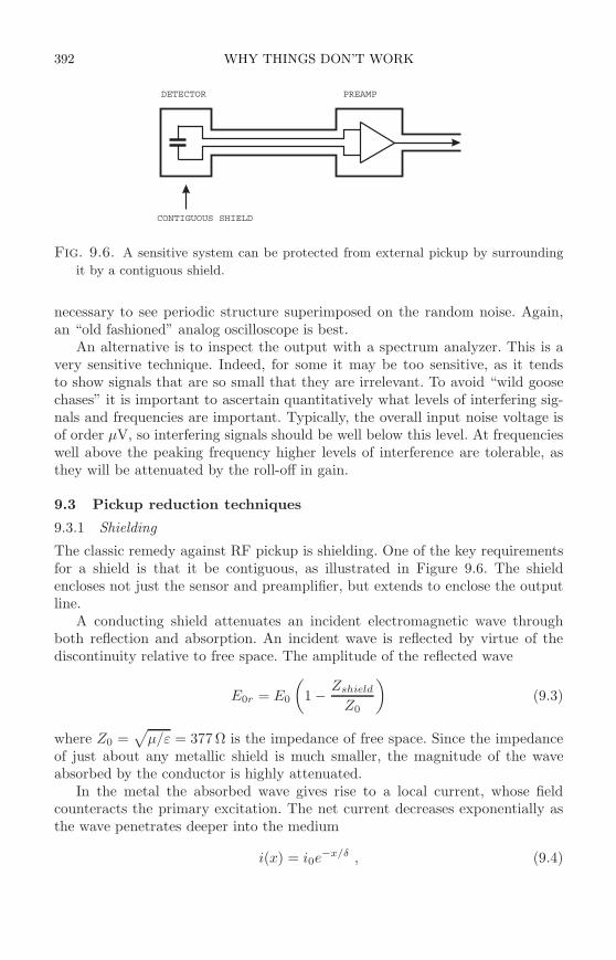
392 WHY THINGS DON’T WORK
DETECTOR PREAMP
CONTIGUOUS SHIELD
Fig. 9.6. A sensitive system can be protected from external pickup by surrounding
it by a contiguous shield.
necessary to see periodic structure superimposed on the random noise. Again,an “old fashioned” analog oscilloscope is best.
An alternative is to inspect the output with a spectrum analyzer. This is avery sensitive technique. Indeed, for some it may be too sensitive, as it tendsto show signals that are so small that they are irrelevant. To avoid “wild goosechases” it is important to ascertain quantitatively what levels of interfering sig-nals and frequencies are important. Typically, the overall input noise voltage isof order µV, so interfering signals should be well below this level. At frequencieswell above the peaking frequency higher levels of interference are tolerable, asthey will be attenuated by the roll-off in gain.
9.3 Pickup reduction techniques
9.3.1 Shielding
The classic remedy against RF pickup is shielding. One of the key requirementsfor a shield is that it be contiguous, as illustrated in Figure 9.6. The shieldencloses not just the sensor and preamplifier, but extends to enclose the outputline.
A conducting shield attenuates an incident electromagnetic wave throughboth reflection and absorption. An incident wave is reflected by virtue of thediscontinuity relative to free space. The amplitude of the reflected wave
E0r = E0
(
1 − Zshield
Z0
)
(9.3)
where Z0 =√
µ/ε = 377 Ω is the impedance of free space. Since the impedanceof just about any metallic shield is much smaller, the magnitude of the waveabsorbed by the conductor is highly attenuated.
In the metal the absorbed wave gives rise to a local current, whose fieldcounteracts the primary excitation. The net current decreases exponentially asthe wave penetrates deeper into the medium
i(x) = i0e−x/δ , (9.4)
PICKUP REDUCTION TECHNIQUES 393
Fig. 9.7. Currents induced on the outside surface of a shield by can flow to the inside
through holes or slots.
where i0 is the current at the surface of the conductor and
δ =1
2 · 10−4
[√
cm
s
]√
ρ
µrf(9.5)
is the penetration depth or “skin depth”. µr and ρ are the permeability and resis-tivity of the conductor and f is the frequency of the incident wave. In aluminum,ρ = 2.8 µΩ cm and µr = 1, so at f = 1MHz the skin depth δ = 84 µm ≈ 100 µm.
The skin depth decreases with the square root of increasing frequency anddecreasing resistivity (increasing conductivity). If the shield is sufficiently thick,the skin effect isolates the inner surface of a shielding enclosure from the outersurface. However, this isolation only obtains if no openings in the shield allow theprimary current to flow from the outside to the inside. The shape of the openingis less important than its maximum dimension. For example, a slot acts like adipole antenna and has zero attenuation at the frequency where the slot’s lengthis a half wavelength. For slots whose length l is less then a half wavelength theattenuation of penetrating currents is
A ≈(
2l
λ
)2
. (9.6)
When N small openings are closely spaced, as in a perforated shield, the leakageincreases by
√N . Since leakage depends primarily on the maximum linear di-
mension, rather than the area, a linear array of small holes has less leakage thana slot of the same length and width. Pickup is larger than would be expectedfor a plane wave impinging on the aperture, as the whole outside surface is thecapture area. The induced current is then transferred through the opening, asillustrated in 9.7, albeit with attenuation.
The leakage through an opening can be reduced substantially by configuringit as a waveguide below cutoff. A circular tube of diameter d acts as a waveguideat frequencies above a cutoff frequency
fc =2.7× 10⁹ [Hz · cm]
d. (9.7)
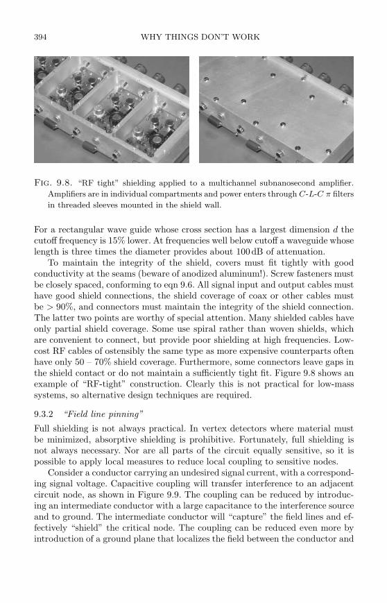
394 WHY THINGS DON’T WORK
Fig. 9.8. “RF tight” shielding applied to a multichannel subnanosecond amplifier.
Amplifiers are in individual compartments and power enters through C-L-C π filters
in threaded sleeves mounted in the shield wall.
For a rectangular wave guide whose cross section has a largest dimension d thecutoff frequency is 15% lower. At frequencies well below cutoff a waveguide whoselength is three times the diameter provides about 100dB of attenuation.
To maintain the integrity of the shield, covers must fit tightly with goodconductivity at the seams (beware of anodized aluminum!). Screw fasteners mustbe closely spaced, conforming to eqn 9.6. All signal input and output cables musthave good shield connections, the shield coverage of coax or other cables mustbe > 90%, and connectors must maintain the integrity of the shield connection.The latter two points are worthy of special attention. Many shielded cables haveonly partial shield coverage. Some use spiral rather than woven shields, whichare convenient to connect, but provide poor shielding at high frequencies. Low-cost RF cables of ostensibly the same type as more expensive counterparts oftenhave only 50 – 70% shield coverage. Furthermore, some connectors leave gaps inthe shield contact or do not maintain a sufficiently tight fit. Figure 9.8 shows anexample of “RF-tight” construction. Clearly this is not practical for low-masssystems, so alternative design techniques are required.
9.3.2 “Field line pinning”
Full shielding is not always practical. In vertex detectors where material mustbe minimized, absorptive shielding is prohibitive. Fortunately, full shielding isnot always necessary. Nor are all parts of the circuit equally sensitive, so it ispossible to apply local measures to reduce local coupling to sensitive nodes.
Consider a conductor carrying an undesired signal current, with a correspond-ing signal voltage. Capacitive coupling will transfer interference to an adjacentcircuit node, as shown in Figure 9.9. The coupling can be reduced by introduc-ing an intermediate conductor with a large capacitance to the interference sourceand to ground. The intermediate conductor will “capture” the field lines and ef-fectively “shield” the critical node. The coupling can be reduced even more byintroduction of a ground plane that localizes the field between the conductor and
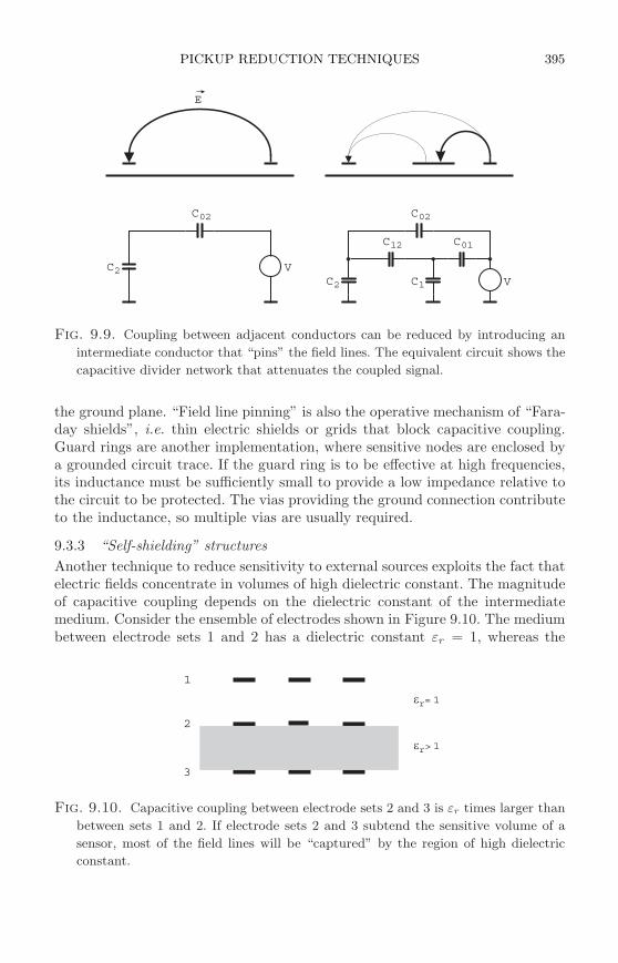
PICKUP REDUCTION TECHNIQUES 395
C
CC
CC
C
C 01
0202
2
2
1
12
E
VV
Fig. 9.9. Coupling between adjacent conductors can be reduced by introducing an
intermediate conductor that “pins” the field lines. The equivalent circuit shows the
capacitive divider network that attenuates the coupled signal.
the ground plane. “Field line pinning” is also the operative mechanism of “Fara-day shields”, i.e. thin electric shields or grids that block capacitive coupling.Guard rings are another implementation, where sensitive nodes are enclosed bya grounded circuit trace. If the guard ring is to be effective at high frequencies,its inductance must be sufficiently small to provide a low impedance relative tothe circuit to be protected. The vias providing the ground connection contributeto the inductance, so multiple vias are usually required.
9.3.3 “Self-shielding” structures
Another technique to reduce sensitivity to external sources exploits the fact thatelectric fields concentrate in volumes of high dielectric constant. The magnitudeof capacitive coupling depends on the dielectric constant of the intermediatemedium. Consider the ensemble of electrodes shown in Figure 9.10. The mediumbetween electrode sets 1 and 2 has a dielectric constant εr = 1, whereas the
r
r
1
2
3
= 1
> 1
Fig. 9.10. Capacitive coupling between electrode sets 2 and 3 is εr times larger than
between sets 1 and 2. If electrode sets 2 and 3 subtend the sensitive volume of a
sensor, most of the field lines will be “captured” by the region of high dielectric
constant.
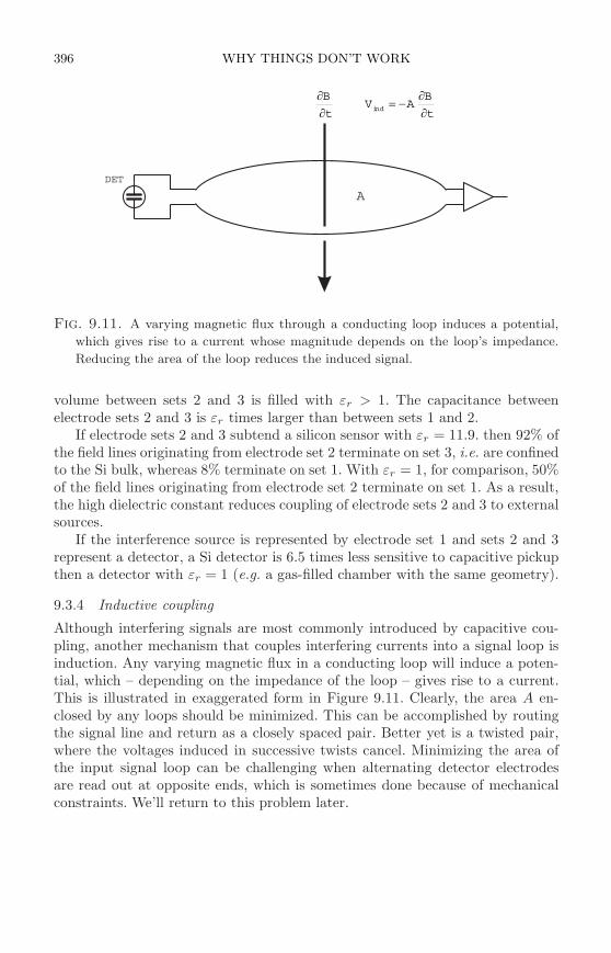
396 WHY THINGS DON’T WORK
DET
B
t
ind
BV A
t
A
Fig. 9.11. A varying magnetic flux through a conducting loop induces a potential,
which gives rise to a current whose magnitude depends on the loop’s impedance.
Reducing the area of the loop reduces the induced signal.
volume between sets 2 and 3 is filled with εr > 1. The capacitance betweenelectrode sets 2 and 3 is εr times larger than between sets 1 and 2.
If electrode sets 2 and 3 subtend a silicon sensor with εr = 11.9. then 92% ofthe field lines originating from electrode set 2 terminate on set 3, i.e. are confinedto the Si bulk, whereas 8% terminate on set 1. With εr = 1, for comparison, 50%of the field lines originating from electrode set 2 terminate on set 1. As a result,the high dielectric constant reduces coupling of electrode sets 2 and 3 to externalsources.
If the interference source is represented by electrode set 1 and sets 2 and 3represent a detector, a Si detector is 6.5 times less sensitive to capacitive pickupthen a detector with εr = 1 (e.g. a gas-filled chamber with the same geometry).
9.3.4 Inductive coupling
Although interfering signals are most commonly introduced by capacitive cou-pling, another mechanism that couples interfering currents into a signal loop isinduction. Any varying magnetic flux in a conducting loop will induce a poten-tial, which – depending on the impedance of the loop – gives rise to a current.This is illustrated in exaggerated form in Figure 9.11. Clearly, the area A en-closed by any loops should be minimized. This can be accomplished by routingthe signal line and return as a closely spaced pair. Better yet is a twisted pair,where the voltages induced in successive twists cancel. Minimizing the area ofthe input signal loop can be challenging when alternating detector electrodesare read out at opposite ends, which is sometimes done because of mechanicalconstraints. We’ll return to this problem later.
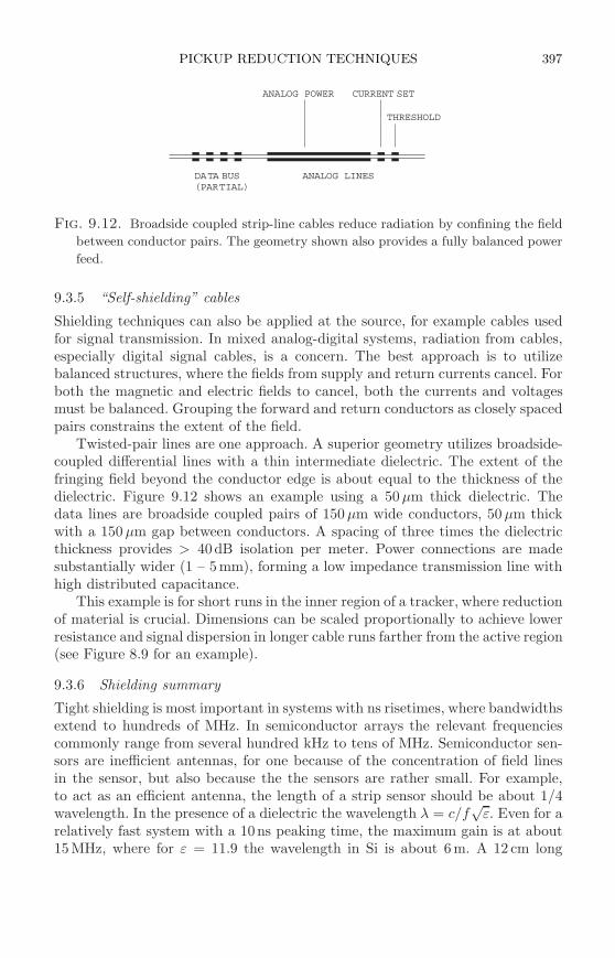
PICKUP REDUCTION TECHNIQUES 397
ANALOG LINESDATA BUS(PARTIAL)
THRESHOLD
ANALOG POWER CURRENT SET
Fig. 9.12. Broadside coupled strip-line cables reduce radiation by confining the field
between conductor pairs. The geometry shown also provides a fully balanced power
feed.
9.3.5 “Self-shielding” cables
Shielding techniques can also be applied at the source, for example cables usedfor signal transmission. In mixed analog-digital systems, radiation from cables,especially digital signal cables, is a concern. The best approach is to utilizebalanced structures, where the fields from supply and return currents cancel. Forboth the magnetic and electric fields to cancel, both the currents and voltagesmust be balanced. Grouping the forward and return conductors as closely spacedpairs constrains the extent of the field.
Twisted-pair lines are one approach. A superior geometry utilizes broadside-coupled differential lines with a thin intermediate dielectric. The extent of thefringing field beyond the conductor edge is about equal to the thickness of thedielectric. Figure 9.12 shows an example using a 50µm thick dielectric. Thedata lines are broadside coupled pairs of 150µm wide conductors, 50 µm thickwith a 150 µm gap between conductors. A spacing of three times the dielectricthickness provides > 40dB isolation per meter. Power connections are madesubstantially wider (1 – 5mm), forming a low impedance transmission line withhigh distributed capacitance.
This example is for short runs in the inner region of a tracker, where reductionof material is crucial. Dimensions can be scaled proportionally to achieve lowerresistance and signal dispersion in longer cable runs farther from the active region(see Figure 8.9 for an example).
9.3.6 Shielding summary
Tight shielding is most important in systems with ns risetimes, where bandwidthsextend to hundreds of MHz. In semiconductor arrays the relevant frequenciescommonly range from several hundred kHz to tens of MHz. Semiconductor sen-sors are inefficient antennas, for one because of the concentration of field linesin the sensor, but also because the the sensors are rather small. For example,to act as an efficient antenna, the length of a strip sensor should be about 1/4wavelength. In the presence of a dielectric the wavelength λ = c/f
√ε. Even for a
relatively fast system with a 10ns peaking time, the maximum gain is at about15MHz, where for ε = 11.9 the wavelength in Si is about 6m. A 12 cm long
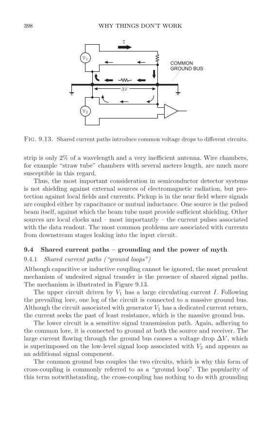
398 WHY THINGS DON’T WORK
V
V
V
1
2
I
COMMON
GROUND BUS
Fig. 9.13. Shared current paths introduce common voltage drops to different circuits.
strip is only 2% of a wavelength and a very inefficient antenna. Wire chambers,for example “straw tube” chambers with several meters length, are much moresusceptible in this regard.
Thus, the most important consideration in semiconductor detector systemsis not shielding against external sources of electromagnetic radiation, but pro-tection against local fields and currents. Pickup is in the near field where signalsare coupled either by capacitance or mutual inductance. One source is the pulsedbeam itself, against which the beam tube must provide sufficient shielding. Othersources are local clocks and – most importantly – the current pulses associatedwith the data readout. The most common problems are associated with currentsfrom downstream stages leaking into the input circuit.
9.4 Shared current paths – grounding and the power of myth
9.4.1 Shared current paths (“ground loops”)
Although capacitive or inductive coupling cannot be ignored, the most prevalentmechanism of undesired signal transfer is the presence of shared signal paths.The mechanism is illustrated in Figure 9.13.
The upper circuit driven by V1 has a large circulating current I . Followingthe prevailing lore, one leg of the circuit is connected to a massive ground bus.Although the circuit associated with generator V1 has a dedicated current return,the current seeks the past of least resistance, which is the massive ground bus.
The lower circuit is a sensitive signal transmission path. Again, adhering tothe common lore, it is connected to ground at both the source and receiver. Thelarge current flowing through the ground bus causes a voltage drop ∆V , whichis superimposed on the low-level signal loop associated with V2 and appears asan additional signal component.
The common ground bus couples the two circuits, which is why this form ofcross-coupling is commonly referred to as a “ground loop”. The popularity ofthis term notwithstanding, the cross-coupling has nothing to do with grounding
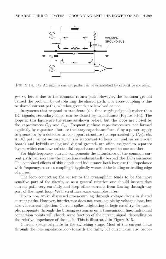
SHARED CURRENT PATHS – GROUNDING AND THE POWER OF MYTH 399
V
V
V
1
2
I
C
Cs2
s1
COMMON
GROUND BUS
Fig. 9.14. For AC signals current paths can be established by capacitive coupling.
per se, but is due to the common return path. However, the common groundcaused the problem by establishing the shared path. The cross-coupling is dueto shared current paths, whether grounds are involved or not.
In systems that respond to transients (i.e. time-varying signals) rather thanDC signals, secondary loops can be closed by capacitance (Figure 9.14). Theloops in this figure are the same as shown before, but the loops are closed bythe capacitances Cs1 and Cs2. Frequently, these capacitances are not formedexplicitly by capacitors, but are the stray capacitance formed by a power supplyto ground or by a detector to its support structure (as represented by Cs2), etc.A DC path is not necessary. This is important to keep in mind, as on circuitboards and hybrids analog and digital grounds are often assigned to separatelayers, which can have substantial capacitance with respect to one another.
For high-frequency current components the inductance of the common cur-rent path can increase the impedance substantially beyond the DC resistance.The combined effects of skin depth and inductance both increase the impedancewith frequency, so cross-coupling is typically worse at the leading or trailing edgeof pulses.
The loop connecting the sensor to the preamplifier tends to be the mostsensitive part of the circuit, so as a general criterion one should inspect thatcurrent path very carefully and keep other currents from flowing through anypart of the input loop. We’ll scrutinize some examples later.
Up to now we’ve discussed cross-coupling through voltage drops in sharedcurrent paths. However, interference does not cross-couple by voltage alone, butalso via current injection. Current spikes originating in logic circuitry, for exam-ple, propagate through the bussing system as on a transmission line. Individualconnection points will absorb some fraction of the current signal, depending onthe relative impedance of the node. This is illustrated in Figure 9.15.
Current spikes originate in the switching stage. Most of the current flowsthrough the low-impedance loop towards the right, but current can also propa-
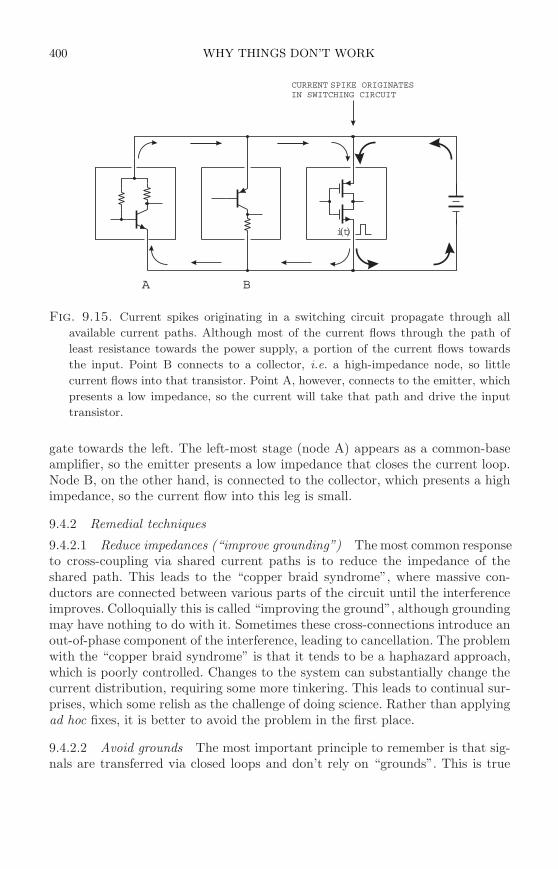
400 WHY THINGS DON’T WORK
it( )
CURRENT SPIKE ORIGINATESIN SWITCHING CIRCUIT
A B
Fig. 9.15. Current spikes originating in a switching circuit propagate through all
available current paths. Although most of the current flows through the path of
least resistance towards the power supply, a portion of the current flows towards
the input. Point B connects to a collector, i.e. a high-impedance node, so little
current flows into that transistor. Point A, however, connects to the emitter, which
presents a low impedance, so the current will take that path and drive the input
transistor.
gate towards the left. The left-most stage (node A) appears as a common-baseamplifier, so the emitter presents a low impedance that closes the current loop.Node B, on the other hand, is connected to the collector, which presents a highimpedance, so the current flow into this leg is small.
9.4.2 Remedial techniques
9.4.2.1 Reduce impedances (“improve grounding”) The most common responseto cross-coupling via shared current paths is to reduce the impedance of theshared path. This leads to the “copper braid syndrome”, where massive con-ductors are connected between various parts of the circuit until the interferenceimproves. Colloquially this is called “improving the ground”, although groundingmay have nothing to do with it. Sometimes these cross-connections introduce anout-of-phase component of the interference, leading to cancellation. The problemwith the “copper braid syndrome” is that it tends to be a haphazard approach,which is poorly controlled. Changes to the system can substantially change thecurrent distribution, requiring some more tinkering. This leads to continual sur-prises, which some relish as the challenge of doing science. Rather than applyingad hoc fixes, it is better to avoid the problem in the first place.
9.4.2.2 Avoid grounds The most important principle to remember is that sig-nals are transferred via closed loops and don’t rely on “grounds”. This is true
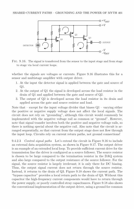
SHARED CURRENT PATHS – GROUNDING AND THE POWER OF MYTH 401
OUTPUT
+V
+V
V
V
DET
DET
DETECTOR
Q1
Q2
Q3
Fig. 9.16. The signal is transferred from the sensor to the input stage and from stage
to stage via local current loops.
whether the signals are voltages or currents. Figure 9.16 illustrates this for asensor and multistage amplifier with output driver.
1. At the input the detector signal is applied between the gate and source ofQ1.
2. At the output of Q1 the signal is developed across the load resistor in thedrain of Q1 and applied between the gate and source of Q2.
3. The output of Q2 is developed across the load resistor in its drain andapplied across the gate and source resistor and load.
Note that – except for the input voltage divider that biases Q1 – varying eitherthe positive or negative supply voltage does not affect the local signals. Thecircuit does not rely on “grounding”, although this circuit would commonly beimplemented with the negative voltage rail as common or “ground”. However,note that signal transfer involves both the positive and negative voltage rails, sothere is nothing special about the negative rail. Also note that the circuit is ar-ranged sequentially, so that current from the output stage does not flow throughthe input loop. Circuits rely on current return paths, not ground connections!
9.4.2.3 Control signal paths Let’s extend the circuit in Figure 9.16 to includean external data acquisition system, as shown in Figure 9.17. The output driveris an example of an extended local loop. To provide sufficient current drive for thetransmission line the driver is configured as a source follower. The source resistoris chosen to be large compared to the termination resistor in the DAQ systemand also large compared to the output resistance of the source follower. For thesignal, the source resistor is largely irrelevant; it is only there for DC biasing.Thus, the output signal current does not return through the source resistor.Instead, it returns to the drain of Q3. Figure 9.18 shows the current path. The“bypass capacitor” provides a local return path to the drain of Q3. Without thiscapacitor the high-frequency current components would have to return throughthe power supply, or poorly controlled stray capacitances. Figure 9.18 also showsthe conventional implementation of the output driver, using a ground for common
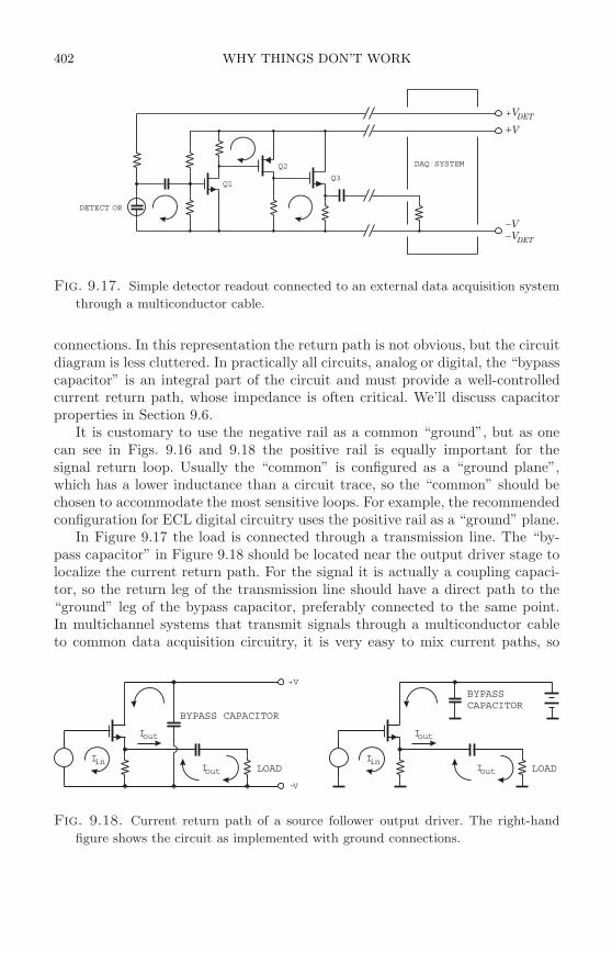
402 WHY THINGS DON’T WORK
DAQ SYSTEM
+V
+V
V
V
DET
DET
Q1
Q2
Q3
DETECT OR
Fig. 9.17. Simple detector readout connected to an external data acquisition system
through a multiconductor cable.
connections. In this representation the return path is not obvious, but the circuitdiagram is less cluttered. In practically all circuits, analog or digital, the “bypasscapacitor” is an integral part of the circuit and must provide a well-controlledcurrent return path, whose impedance is often critical. We’ll discuss capacitorproperties in Section 9.6.
It is customary to use the negative rail as a common “ground”, but as onecan see in Figs. 9.16 and 9.18 the positive rail is equally important for thesignal return loop. Usually the “common” is configured as a “ground plane”,which has a lower inductance than a circuit trace, so the “common” should bechosen to accommodate the most sensitive loops. For example, the recommendedconfiguration for ECL digital circuitry uses the positive rail as a “ground” plane.
In Figure 9.17 the load is connected through a transmission line. The “by-pass capacitor” in Figure 9.18 should be located near the output driver stage tolocalize the current return path. For the signal it is actually a coupling capaci-tor, so the return leg of the transmission line should have a direct path to the“ground” leg of the bypass capacitor, preferably connected to the same point.In multichannel systems that transmit signals through a multiconductor cableto common data acquisition circuitry, it is very easy to mix current paths, so
+V
-V
BYPASS CAPACITOR
BYPASSCAPACITOR
LOADLOAD I
I
I
I
IinIinout
out
out
out
Fig. 9.18. Current return path of a source follower output driver. The right-hand
figure shows the circuit as implemented with ground connections.
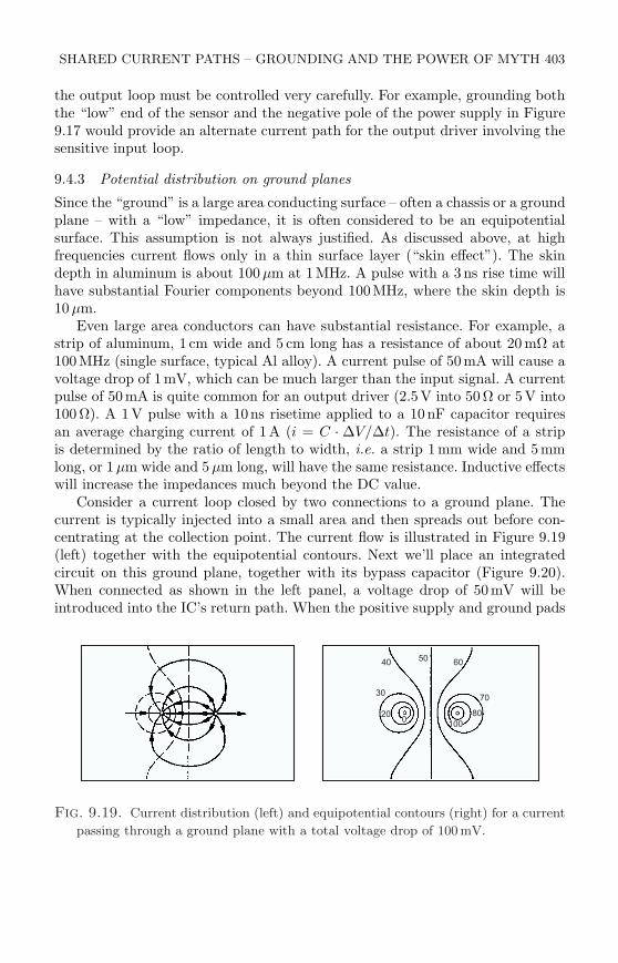
SHARED CURRENT PATHS – GROUNDING AND THE POWER OF MYTH 403
the output loop must be controlled very carefully. For example, grounding boththe “low” end of the sensor and the negative pole of the power supply in Figure9.17 would provide an alternate current path for the output driver involving thesensitive input loop.
9.4.3 Potential distribution on ground planes
Since the “ground” is a large area conducting surface – often a chassis or a groundplane – with a “low” impedance, it is often considered to be an equipotentialsurface. This assumption is not always justified. As discussed above, at highfrequencies current flows only in a thin surface layer (“skin effect”). The skindepth in aluminum is about 100 µm at 1MHz. A pulse with a 3ns rise time willhave substantial Fourier components beyond 100MHz, where the skin depth is10 µm.
Even large area conductors can have substantial resistance. For example, astrip of aluminum, 1 cm wide and 5 cm long has a resistance of about 20 mΩ at100MHz (single surface, typical Al alloy). A current pulse of 50mA will cause avoltage drop of 1mV, which can be much larger than the input signal. A currentpulse of 50mA is quite common for an output driver (2.5V into 50 Ω or 5V into100 Ω). A 1V pulse with a 10ns risetime applied to a 10nF capacitor requiresan average charging current of 1A (i = C · ∆V/∆t). The resistance of a stripis determined by the ratio of length to width, i.e. a strip 1 mm wide and 5mmlong, or 1 µm wide and 5 µm long, will have the same resistance. Inductive effectswill increase the impedances much beyond the DC value.
Consider a current loop closed by two connections to a ground plane. Thecurrent is typically injected into a small area and then spreads out before con-centrating at the collection point. The current flow is illustrated in Figure 9.19(left) together with the equipotential contours. Next we’ll place an integratedcircuit on this ground plane, together with its bypass capacitor (Figure 9.20).When connected as shown in the left panel, a voltage drop of 50mV will beintroduced into the IC’s return path. When the positive supply and ground pads
100
80
70
6050
40
30
200
Fig. 9.19. Current distribution (left) and equipotential contours (right) for a current
passing through a ground plane with a total voltage drop of 100 mV.
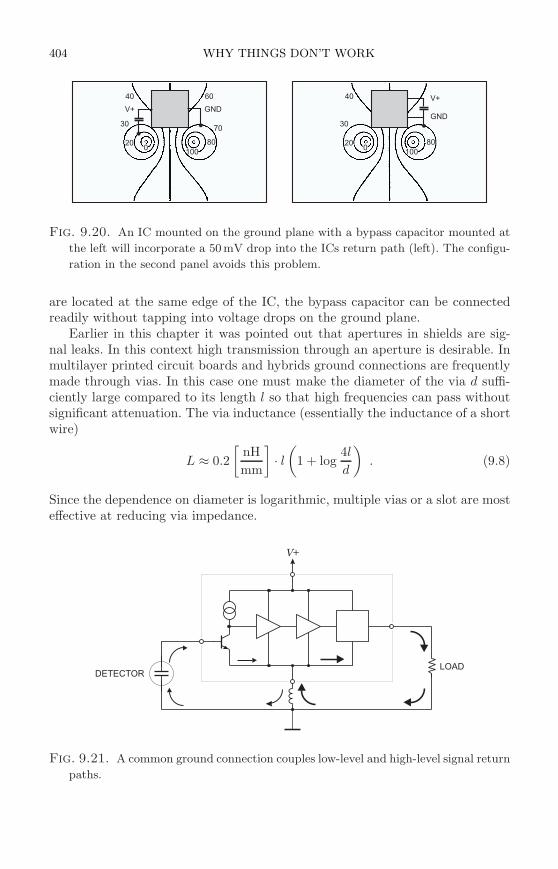
404 WHY THINGS DON’T WORK
100 100
80 80
70
6040 40
30 30
20 200 0
GND
GND
V+
V+
Fig. 9.20. An IC mounted on the ground plane with a bypass capacitor mounted at
the left will incorporate a 50 mV drop into the ICs return path (left). The configu-
ration in the second panel avoids this problem.
are located at the same edge of the IC, the bypass capacitor can be connectedreadily without tapping into voltage drops on the ground plane.
Earlier in this chapter it was pointed out that apertures in shields are sig-nal leaks. In this context high transmission through an aperture is desirable. Inmultilayer printed circuit boards and hybrids ground connections are frequentlymade through vias. In this case one must make the diameter of the via d suffi-ciently large compared to its length l so that high frequencies can pass withoutsignificant attenuation. The via inductance (essentially the inductance of a shortwire)
L ≈ 0.2
[
nH
mm
]
· l(
1 + log4l
d
)
. (9.8)
Since the dependence on diameter is logarithmic, multiple vias or a slot are mosteffective at reducing via impedance.
V+
DETECTORLOAD
Fig. 9.21. A common ground connection couples low-level and high-level signal return
paths.
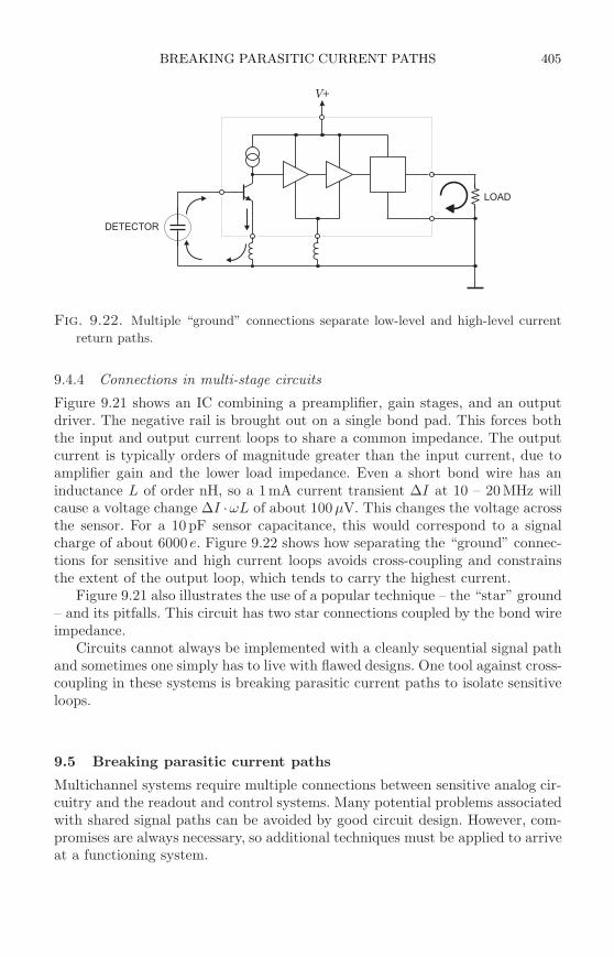
BREAKING PARASITIC CURRENT PATHS 405
LOAD
V+
DETECTOR
Fig. 9.22. Multiple “ground” connections separate low-level and high-level current
return paths.
9.4.4 Connections in multi-stage circuits
Figure 9.21 shows an IC combining a preamplifier, gain stages, and an outputdriver. The negative rail is brought out on a single bond pad. This forces boththe input and output current loops to share a common impedance. The outputcurrent is typically orders of magnitude greater than the input current, due toamplifier gain and the lower load impedance. Even a short bond wire has aninductance L of order nH, so a 1mA current transient ∆I at 10 – 20MHz willcause a voltage change ∆I ·ωL of about 100µV. This changes the voltage acrossthe sensor. For a 10pF sensor capacitance, this would correspond to a signalcharge of about 6000 e. Figure 9.22 shows how separating the “ground” connec-tions for sensitive and high current loops avoids cross-coupling and constrainsthe extent of the output loop, which tends to carry the highest current.
Figure 9.21 also illustrates the use of a popular technique – the “star” ground– and its pitfalls. This circuit has two star connections coupled by the bond wireimpedance.
Circuits cannot always be implemented with a cleanly sequential signal pathand sometimes one simply has to live with flawed designs. One tool against cross-coupling in these systems is breaking parasitic current paths to isolate sensitiveloops.
9.5 Breaking parasitic current paths
Multichannel systems require multiple connections between sensitive analog cir-cuitry and the readout and control systems. Many potential problems associatedwith shared signal paths can be avoided by good circuit design. However, com-promises are always necessary, so additional techniques must be applied to arriveat a functioning system.
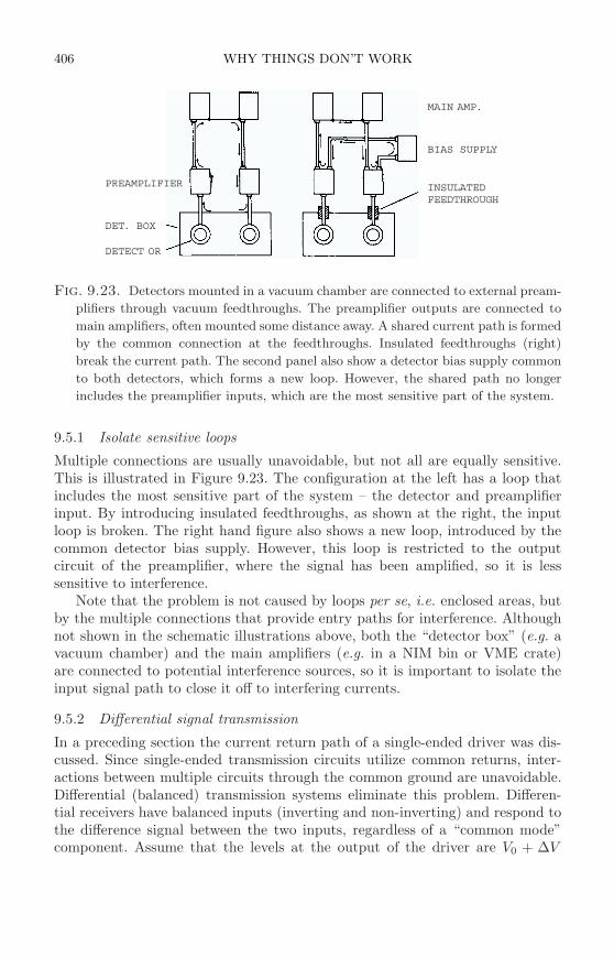
406 WHY THINGS DON’T WORK
DETECT OR
DET. BOX
INSULATEDFEEDTHROUGH
BIAS SUPPLY
MAIN AMP.
PREAMPLIFIER
Fig. 9.23. Detectors mounted in a vacuum chamber are connected to external pream-
plifiers through vacuum feedthroughs. The preamplifier outputs are connected to
main amplifiers, often mounted some distance away. A shared current path is formed
by the common connection at the feedthroughs. Insulated feedthroughs (right)
break the current path. The second panel also show a detector bias supply common
to both detectors, which forms a new loop. However, the shared path no longer
includes the preamplifier inputs, which are the most sensitive part of the system.
9.5.1 Isolate sensitive loops
Multiple connections are usually unavoidable, but not all are equally sensitive.This is illustrated in Figure 9.23. The configuration at the left has a loop thatincludes the most sensitive part of the system – the detector and preamplifierinput. By introducing insulated feedthroughs, as shown at the right, the inputloop is broken. The right hand figure also shows a new loop, introduced by thecommon detector bias supply. However, this loop is restricted to the outputcircuit of the preamplifier, where the signal has been amplified, so it is lesssensitive to interference.
Note that the problem is not caused by loops per se, i.e. enclosed areas, butby the multiple connections that provide entry paths for interference. Althoughnot shown in the schematic illustrations above, both the “detector box” (e.g. avacuum chamber) and the main amplifiers (e.g. in a NIM bin or VME crate)are connected to potential interference sources, so it is important to isolate theinput signal path to close it off to interfering currents.
9.5.2 Differential signal transmission
In a preceding section the current return path of a single-ended driver was dis-cussed. Since single-ended transmission circuits utilize common returns, inter-actions between multiple circuits through the common ground are unavoidable.Differential (balanced) transmission systems eliminate this problem. Differen-tial receivers have balanced inputs (inverting and non-inverting) and respond tothe difference signal between the two inputs, regardless of a “common mode”component. Assume that the levels at the output of the driver are V0 + ∆V
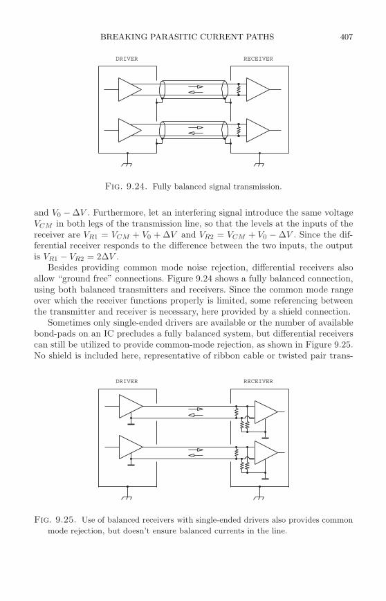
BREAKING PARASITIC CURRENT PATHS 407
DRIVER RECEIVER
Fig. 9.24. Fully balanced signal transmission.
and V0 −∆V . Furthermore, let an interfering signal introduce the same voltageVCM in both legs of the transmission line, so that the levels at the inputs of thereceiver are VR1 = VCM + V0 + ∆V and VR2 = VCM + V0 − ∆V . Since the dif-ferential receiver responds to the difference between the two inputs, the outputis VR1 − VR2 = 2∆V .
Besides providing common mode noise rejection, differential receivers alsoallow “ground free” connections. Figure 9.24 shows a fully balanced connection,using both balanced transmitters and receivers. Since the common mode rangeover which the receiver functions properly is limited, some referencing betweenthe transmitter and receiver is necessary, here provided by a shield connection.
Sometimes only single-ended drivers are available or the number of availablebond-pads on an IC precludes a fully balanced system, but differential receiverscan still be utilized to provide common-mode rejection, as shown in Figure 9.25.No shield is included here, representative of ribbon cable or twisted pair trans-
DRIVER RECEIVER
Fig. 9.25. Use of balanced receivers with single-ended drivers also provides common
mode rejection, but doesn’t ensure balanced currents in the line.
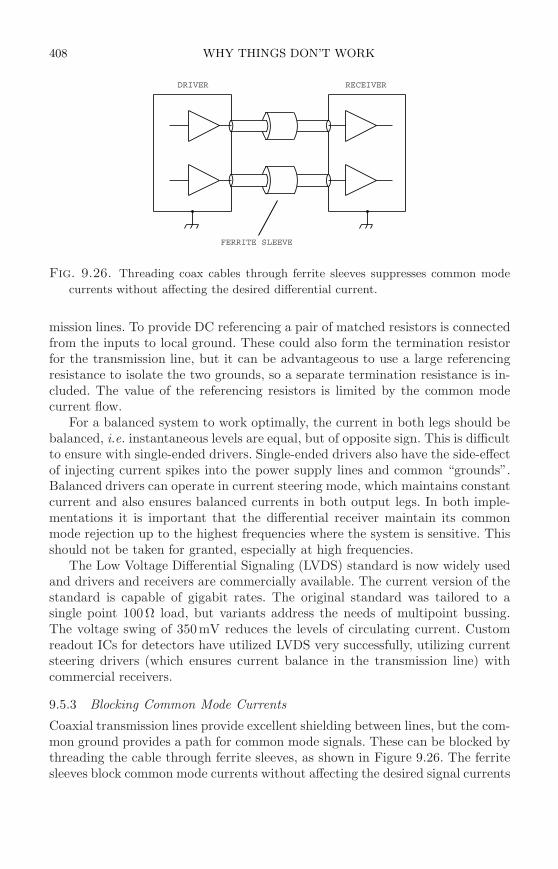
408 WHY THINGS DON’T WORK
FERRITE SLEEVE
DRIVER RECEIVER
Fig. 9.26. Threading coax cables through ferrite sleeves suppresses common mode
currents without affecting the desired differential current.
mission lines. To provide DC referencing a pair of matched resistors is connectedfrom the inputs to local ground. These could also form the termination resistorfor the transmission line, but it can be advantageous to use a large referencingresistance to isolate the two grounds, so a separate termination resistance is in-cluded. The value of the referencing resistors is limited by the common modecurrent flow.
For a balanced system to work optimally, the current in both legs should bebalanced, i.e. instantaneous levels are equal, but of opposite sign. This is difficultto ensure with single-ended drivers. Single-ended drivers also have the side-effectof injecting current spikes into the power supply lines and common “grounds”.Balanced drivers can operate in current steering mode, which maintains constantcurrent and also ensures balanced currents in both output legs. In both imple-mentations it is important that the differential receiver maintain its commonmode rejection up to the highest frequencies where the system is sensitive. Thisshould not be taken for granted, especially at high frequencies.
The Low Voltage Differential Signaling (LVDS) standard is now widely usedand drivers and receivers are commercially available. The current version of thestandard is capable of gigabit rates. The original standard was tailored to asingle point 100Ω load, but variants address the needs of multipoint bussing.The voltage swing of 350mV reduces the levels of circulating current. Customreadout ICs for detectors have utilized LVDS very successfully, utilizing currentsteering drivers (which ensures current balance in the transmission line) withcommercial receivers.
9.5.3 Blocking Common Mode Currents
Coaxial transmission lines provide excellent shielding between lines, but the com-mon ground provides a path for common mode signals. These can be blocked bythreading the cable through ferrite sleeves, as shown in Figure 9.26. The ferritesleeves block common mode currents without affecting the desired signal currents
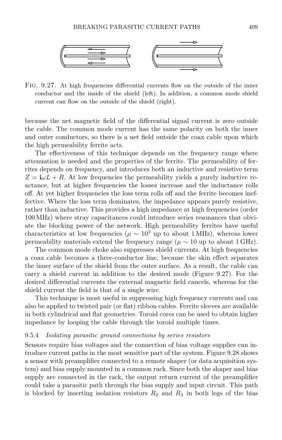
BREAKING PARASITIC CURRENT PATHS 409
Fig. 9.27. At high frequencies differential currents flow on the outside of the inner
conductor and the inside of the shield (left). In addition, a common mode shield
current can flow on the outside of the shield (right).
because the net magnetic field of the differential signal current is zero outsidethe cable. The common mode current has the same polarity on both the innerand outer conductors, so there is a net field outside the coax cable upon whichthe high permeability ferrite acts.
The effectiveness of this technique depends on the frequency range whereattenuation is needed and the properties of the ferrite. The permeability of fer-rites depends on frequency, and introduces both an inductive and resistive termZ = iωL + R. At low frequencies the permeability yields a purely inductive re-actance, but at higher frequencies the losses increase and the inductance rollsoff. At yet higher frequencies the loss term rolls off and the ferrite becomes inef-fective. Where the loss term dominates, the impedance appears purely resistive,rather than inductive. This provides a high impedance at high frequencies (order100MHz) where stray capacitances could introduce series resonances that obvi-ate the blocking power of the network. High permeability ferrites have usefulcharacteristics at low frequencies (µ ∼ 103 up to about 1 MHz), whereas lowerpermeability materials extend the frequency range (µ ∼ 10 up to about 1GHz).
The common mode choke also suppresses shield currents. At high frequenciesa coax cable becomes a three-conductor line, because the skin effect separatesthe inner surface of the shield from the outer surface. As a result, the cable cancarry a shield current in addition to the desired mode (Figure 9.27). For thedesired differential currents the external magnetic field cancels, whereas for theshield current the field is that of a single wire.
This technique is most useful in suppressing high frequency currents and canalso be applied to twisted pair (or flat) ribbon cables. Ferrite sleeves are availablein both cylindrical and flat geometries. Toroid cores can be used to obtain higherimpedance by looping the cable through the toroid multiple times.
9.5.4 Isolating parasitic ground connections by series resistors
Sensors require bias voltages and the connection of bias voltage supplies can in-troduce current paths in the most sensitive part of the system. Figure 9.28 showsa sensor with preamplifier connected to a remote shaper (or data acquisition sys-tem) and bias supply mounted in a common rack. Since both the shaper and biassupply are connected in the rack, the output return current of the preamplifiercould take a parasitic path through the bias supply and input circuit. This pathis blocked by inserting isolation resistors R2 and R3 in both legs of the bias
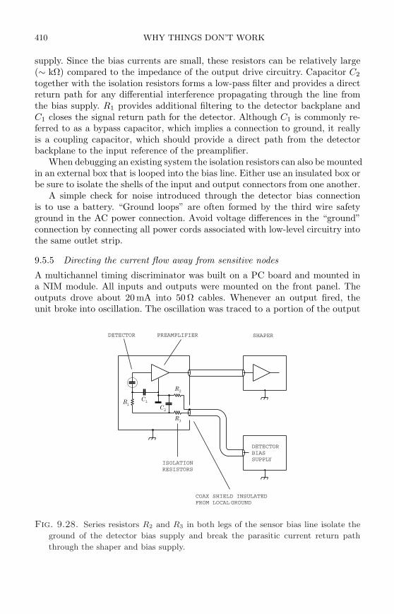
410 WHY THINGS DON’T WORK
supply. Since the bias currents are small, these resistors can be relatively large(∼ kΩ) compared to the impedance of the output drive circuitry. Capacitor C2
together with the isolation resistors forms a low-pass filter and provides a directreturn path for any differential interference propagating through the line fromthe bias supply. R1 provides additional filtering to the detector backplane andC1 closes the signal return path for the detector. Although C1 is commonly re-ferred to as a bypass capacitor, which implies a connection to ground, it reallyis a coupling capacitor, which should provide a direct path from the detectorbackplane to the input reference of the preamplifier.
When debugging an existing system the isolation resistors can also be mountedin an external box that is looped into the bias line. Either use an insulated box orbe sure to isolate the shells of the input and output connectors from one another.
A simple check for noise introduced through the detector bias connectionis to use a battery. “Ground loops” are often formed by the third wire safetyground in the AC power connection. Avoid voltage differences in the “ground”connection by connecting all power cords associated with low-level circuitry intothe same outlet strip.
9.5.5 Directing the current flow away from sensitive nodes
A multichannel timing discriminator was built on a PC board and mounted ina NIM module. All inputs and outputs were mounted on the front panel. Theoutputs drove about 20 mA into 50 Ω cables. Whenever an output fired, theunit broke into oscillation. The oscillation was traced to a portion of the output
DETECTORBIASSUPPLY
SHAPER
COAX SHIELD INSULATEDFROM LOCAL GROUND
ISOLATIONRESISTORS
DETECTOR PREAMPLIFIER
RC
C
R
R
11
2
3
2
Fig. 9.28. Series resistors R2 and R3 in both legs of the sensor bias line isolate the
ground of the detector bias supply and break the parasitic current return path
through the shaper and bias supply.
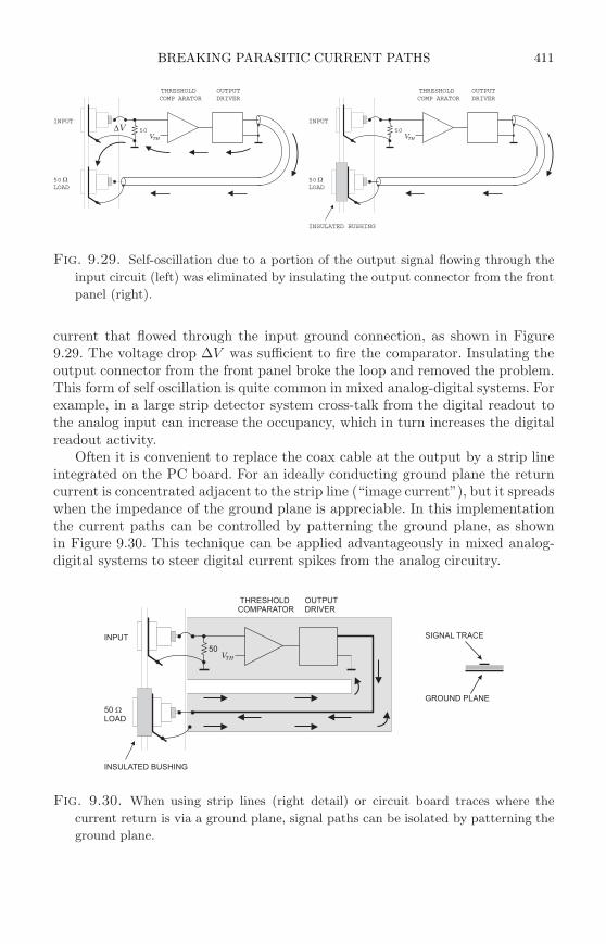
BREAKING PARASITIC CURRENT PATHS 411
50 50
THRESHOLDCOMP ARATOR
THRESHOLDCOMP ARATOR
OUTPUTDRIVER
OUTPUTDRIVER
V VTH TH
V
50LOAD
50LOAD
INSULATED BUSHING
INPUT INPUT
Fig. 9.29. Self-oscillation due to a portion of the output signal flowing through the
input circuit (left) was eliminated by insulating the output connector from the front
panel (right).
current that flowed through the input ground connection, as shown in Figure9.29. The voltage drop ∆V was sufficient to fire the comparator. Insulating theoutput connector from the front panel broke the loop and removed the problem.This form of self oscillation is quite common in mixed analog-digital systems. Forexample, in a large strip detector system cross-talk from the digital readout tothe analog input can increase the occupancy, which in turn increases the digitalreadout activity.
Often it is convenient to replace the coax cable at the output by a strip lineintegrated on the PC board. For an ideally conducting ground plane the returncurrent is concentrated adjacent to the strip line (“image current”), but it spreadswhen the impedance of the ground plane is appreciable. In this implementationthe current paths can be controlled by patterning the ground plane, as shownin Figure 9.30. This technique can be applied advantageously in mixed analog-digital systems to steer digital current spikes from the analog circuitry.
Fig. 9.30. When using strip lines (right detail) or circuit board traces where the
current return is via a ground plane, signal paths can be isolated by patterning the
ground plane.
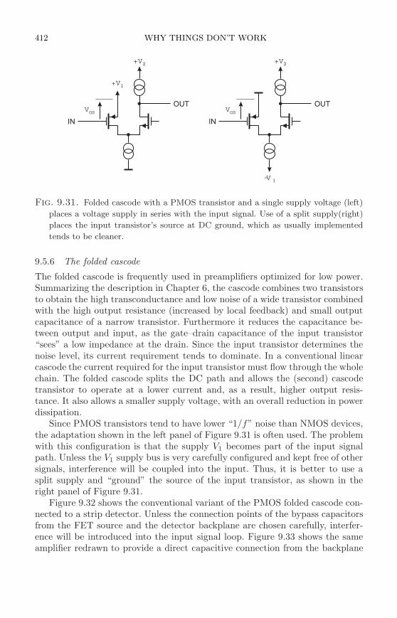
412 WHY THINGS DON’T WORK
ININ
OUTOUTVV
-V
+V
+V+V
GSGS
1
1
22
Fig. 9.31. Folded cascode with a PMOS transistor and a single supply voltage (left)
places a voltage supply in series with the input signal. Use of a split supply(right)
places the input transistor’s source at DC ground, which as usually implemented
tends to be cleaner.
9.5.6 The folded cascode
The folded cascode is frequently used in preamplifiers optimized for low power.Summarizing the description in Chapter 6, the cascode combines two transistorsto obtain the high transconductance and low noise of a wide transistor combinedwith the high output resistance (increased by local feedback) and small outputcapacitance of a narrow transistor. Furthermore it reduces the capacitance be-tween output and input, as the gate–drain capacitance of the input transistor“sees” a low impedance at the drain. Since the input transistor determines thenoise level, its current requirement tends to dominate. In a conventional linearcascode the current required for the input transistor must flow through the wholechain. The folded cascode splits the DC path and allows the (second) cascodetransistor to operate at a lower current and, as a result, higher output resis-tance. It also allows a smaller supply voltage, with an overall reduction in powerdissipation.
Since PMOS transistors tend to have lower “1/f” noise than NMOS devices,the adaptation shown in the left panel of Figure 9.31 is often used. The problemwith this configuration is that the supply V1 becomes part of the input signalpath. Unless the V1 supply bus is very carefully configured and kept free of othersignals, interference will be coupled into the input. Thus, it is better to use asplit supply and “ground” the source of the input transistor, as shown in theright panel of Figure 9.31.
Figure 9.32 shows the conventional variant of the PMOS folded cascode con-nected to a strip detector. Unless the connection points of the bypass capacitorsfrom the FET source and the detector backplane are chosen carefully, interfer-ence will be introduced into the input signal loop. Figure 9.33 shows the sameamplifier redrawn to provide a direct capacitive connection from the backplane
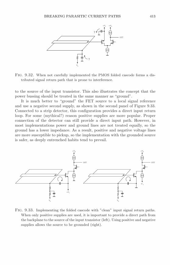
BREAKING PARASITIC CURRENT PATHS 413
OUT
V
+V +V
b
1 2
?
?
Fig. 9.32. When not carefully implemented the PMOS folded cascode forms a dis-
tributed signal return path that is prone to interference.
to the source of the input transistor. This also illustrates the concept that thepower bussing should be treated in the same manner as “ground”.
It is much better to “ground” the FET source to a local signal referenceand use a negative second supply, as shown in the second panel of Figure 9.33.Connected to a strip detector, this configuration provides a direct input returnloop. For some (mythical?) reason positive supplies are more popular. Properconnection of the detector can still provide a direct input path. However, inmost implementations power and ground lines are not treated equally, so theground has a lower impedance. As a result, positive and negative voltage linesare more susceptible to pickup, so the implementation with the grounded sourceis safer, as deeply entrenched habits tend to prevail.
OUT OUT
V V
+V
-V
+V +V
b b
1
1
2 2
Fig. 9.33. Implementing the folded cascode with ”clean” input signal return paths.
When only positive supplies are used, it is important to provide a direct path from
the backplane to the source of the input transistor (left). Using positive and negative
supplies allows the source to be grounded (right).
414 WHY THINGS DON’T WORK
9.6 Capacitors
The preceding discussions have underscored the key role of “bypass” capacitorsin the signal path. When used to close low-impedance loops, as in bypass capac-itors at IC power connections, the impedance must be small. Although drawnas an ideal capacitor in circuit diagrams, it is important to remember that ev-ery capacitor also has a series inductance and resistance. The capacitance andinductance form a series resonant circuit. At resonance the impedance is limitedby the series resistance and above resonance the capacitor appears inductive.The frequency response is complicated by the fact that the equivalent series re-sistance is frequency dependent. When in the signal path, the capacitor’s seriesresistance can introduce noise.
The inductance depends on the geometry. Foil capacitors are commonly madeof thin metallized layers of plastic, often rolled into a cylinder, but also availableas rectangular stacks. These capacitors tend to have a rather high inductanceand their use is limited to frequencies up to hundreds of kHz or so. In tantalumelectrolytic capacitors the dielectric is formed as an oxide on a rough surfaceor sponge-like electrode. These devices provide capacitance up to hundreds ofµF and are usable into the MHz range. However, they have poor tolerances andlarge temperature coefficients. The lowest inductance is provided by multilayerceramic chip capacitors, where many layers of metallized ceramic are fused to-gether. Essentially, these are many small capacitors connected in parallel, sothe inductance is reduced correspondingly. Multilayer ceramic capacitors are thedevices of choice in high frequency applications, especially when used as chipcapacitors, which practically eliminate the lead inductance. However, there aresignificant differences between the dielectrics used in these devices.
The dielectrics are BaTiO5 based, diluted with rare earth oxides. Z5U or Y5Vdielectrics have dielectric constants up to 2·104, so they provide high capacitancein a small volume. For example, a 0.1 µF/16 V capacitor has a footprint of 1.6×0.8mm2 with a thickness of 0.9mm. Available capacitances range into the 10sof µF. These dielectrics have a large voltage coefficient. Operated at their ratedvoltage the capacitance of Y5V capacitors can be as small as 20% of the valueat zero volts. The capacitance also shows a strong frequency dependence.
X7R has a dielectric constant of about 103. The capacitance variation withfrequency is about 20% from 1kHz to 10MHz and the voltage coefficient is small.Maximum capacitance is several µF.
The highest quality ceramic dielectric is NP0 (“negative positive zero”) witha temperature coefficient of ±30ppm/
C and practically no dependence of ca-
pacitance vs. frequency. The capacitance is limited to about 10nF.Since the dielectrics are piezoelectric, ceramic capacitors are microphonic.
Application of a 1 kHz alternating voltage can make a capacitor “sing”. Con-versely, vibration will translate into voltage changes. Z5U and Y5U are mostsusceptible.
Figure 9.34 shows the impedance vs. frequency for various capacitors. Theinductance is determined by the size of the package and is of order nH. For a given
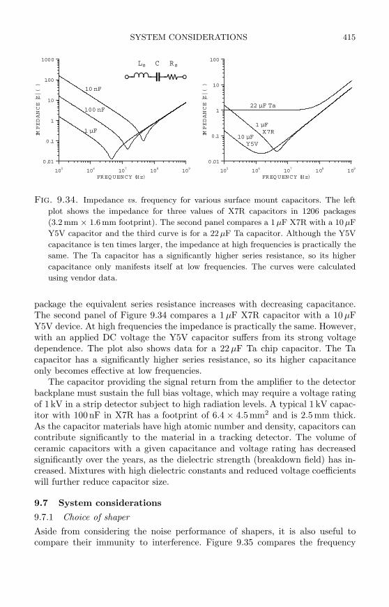
SYSTEM CONSIDERATIONS 415
105
106
107
108
109
FREQUENCY (Hz)
0.01
0.1
1
10
100
1000
IMPEDANCE|Z|()
10 nF
105
106
107
108
109
FREQUENCY (Hz)
0.01
0.1
1
10
100
IMPEDANCE|Z|()
1 µFX7R
100 nF
1 µF10 µF
Y5V
22 µF Ta
CL Rs s
Fig. 9.34. Impedance vs. frequency for various surface mount capacitors. The left
plot shows the impedance for three values of X7R capacitors in 1206 packages
(3.2 mm × 1.6 mm footprint). The second panel compares a 1 µF X7R with a 10 µF
Y5V capacitor and the third curve is for a 22 µF Ta capacitor. Although the Y5V
capacitance is ten times larger, the impedance at high frequencies is practically the
same. The Ta capacitor has a significantly higher series resistance, so its higher
capacitance only manifests itself at low frequencies. The curves were calculated
using vendor data.
package the equivalent series resistance increases with decreasing capacitance.The second panel of Figure 9.34 compares a 1µF X7R capacitor with a 10 µFY5V device. At high frequencies the impedance is practically the same. However,with an applied DC voltage the Y5V capacitor suffers from its strong voltagedependence. The plot also shows data for a 22µF Ta chip capacitor. The Tacapacitor has a significantly higher series resistance, so its higher capacitanceonly becomes effective at low frequencies.
The capacitor providing the signal return from the amplifier to the detectorbackplane must sustain the full bias voltage, which may require a voltage ratingof 1 kV in a strip detector subject to high radiation levels. A typical 1 kV capac-itor with 100nF in X7R has a footprint of 6.4 × 4.5mm2 and is 2.5mm thick.As the capacitor materials have high atomic number and density, capacitors cancontribute significantly to the material in a tracking detector. The volume ofceramic capacitors with a given capacitance and voltage rating has decreasedsignificantly over the years, as the dielectric strength (breakdown field) has in-creased. Mixtures with high dielectric constants and reduced voltage coefficientswill further reduce capacitor size.
9.7 System considerations
9.7.1 Choice of shaper
Aside from considering the noise performance of shapers, it is also useful tocompare their immunity to interference. Figure 9.35 compares the frequency
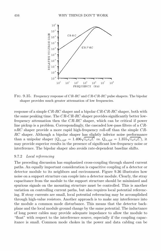
416 WHY THINGS DON’T WORK
102 103 104 105 106 107 108
FREQUENCY (Hz)
10-9
10-8
10-7
10-6
10-5
10-4
10-3
10-2
10-1
100
RELATIVEVOLTAGEGAIN
(CR)2-RC
CR-RC
Fig. 9.35. Frequency response of CR-RC and CR-CR-RC pulse shapers. The bipolar
shaper provides much greater attenuation of low frequencies.
response of a simple CR-RC shaper and a bipolar CR-CR-RC shaper, both withthe same peaking time. The CR-CR-RC shaper provides significantly better low-frequency attenuation then the CR-RC shaper, which can be critical if powerline pickup is a problem. Correspondingly, the cascaded low-pass filters of a CR-nRC shaper provide a more rapid high-frequency roll-off than the simple CR-RC shaper. Although a bipolar shaper has slightly inferior noise performancethan a unipolar shaper (Qn,opt = 1.406
√inenC vs. Qn,opt = 1.355
√inenC), it
may provide superior results in the presence of significant low-frequency noise orinterference. The bipolar shaper also avoids rate-dependent baseline shifts.
9.7.2 Local referencing
The preceding discussion has emphasized cross-coupling through shared currentpaths. An equally important consideration is capacitive coupling of a detector ordetector module to its neighbors and environment. Figure 9.36 illustrates hownoise on a support structure can couple into a detector module. Clearly, the straycapacitance from the module to the support structure should be minimized andspurious signals on the mounting structure must be controlled. This is anothervariation on controlling current paths, but also requires local potential referenc-ing. If stray currents are small, local potential referencing may be accomplishedthrough high-value resistors. Another approach is to make any interference intothe module a common mode disturbance. This means that the detector back-plane and the local module ground change by the same potential. The inductanceof long power cables may provide adequate impedance to allow the module to“float” with respect to the interference source, especially if the coupling capac-itance is small. Common mode chokes in the power and data cabling can be
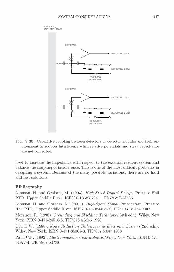
SYSTEM CONSIDERATIONS 417
DETECTOR BIAS
DETECTOR BIAS
SIGNAL OUTPUT
SIGNAL OUTPUT
DETECTOR
DETECTOR
ISOLATIONRESISTORS
ISOLATIONRESISTORS
SUPPORT /COOLING STAVE
Fig. 9.36. Capacitive coupling between detectors or detector modules and their en-
vironment introduces interference when relative potentials and stray capacitance
are not controlled.
used to increase the impedance with respect to the external readout system andbalance the coupling of interference. This is one of the most difficult problems indesigning a system. Because of the many possible variations, there are no hardand fast solutions.
Bibliography
Johnson, H. and Graham, M. (1993). High-Speed Digital Design. Prentice HallPTR, Upper Saddle River. ISBN 0-13-395724-1, TK7868.D5J635
Johnson, H. and Graham, M. (2002). High-Speed Signal Propagation. PrenticeHall PTR, Upper Saddle River, ISBN 0-13-084408-X, TK5103.15.J64 2002
Morrison, R. (1998). Grounding and Shielding Techniques (4th edn). Wiley, NewYork. ISBN 0-471-24518-6, TK7878.4.M66 1998
Ott, H.W. (1988). Noise Reduction Techniques in Electronic Systems(2nd edn).Wiley, New York. ISBN 0-471-85068-3, TK7867.5.087 1988
Paul, C.R. (1992). Electromagnetic Compatibility. Wiley, New York. ISBN 0-471-54927-4, TK 7867.5.P38
APPENDIX A
SEMICONDUCTOR DEVICE TECHNOLOGY
Fabrication of semiconductor devices is a complex technology that uses manydifferent techniques. This is only a brief survey of the key steps to provide a betterunderstanding of the implications in utilizing devices. Many process tutorials canbe found on university web-sites. For a detailed description of modern fabricationtechniques see a recent compilation by Nishi and Doering (2000), for example.Lutz (1999) describes simulations and some aspects of detector fabrication.
The key ingredients of a semiconductor device fabrication process are
1. Bulk material, e.g. Si, Ge, or GaAs.
2. Dopants to create p- and n-type regions.
3. Deposition of contact and insulator films.
4. Patterning to selectively introduce dopants and remove material.
5. Passivation to protect the semiconductor surfaces from damage and con-taminants.
Practically all semiconductor devices are fabricated in a planar geometry. No-table exceptions are large volume detectors for gamma-ray spectroscopy.
A.1 Bulk material
The starting point is a semiconductor wafer, i.e. a slice of silicon from a largecylindrical single crystal (boule). Here detectors differ significantly from inte-grated circuits. Electronic circuitry resides in a thin layer at the wafer surface,whereas in detectors the diode depletion region extends into or throughout thebulk. This requires both high purity and a low density of mechanical micro-defects, e.g. dislocations. This is achieved by growing the crystals using a floatzone process, which through zone refining removes impurities and yields essen-tially dislocation-free crystals. A polysilicon rod is passed through a heatingcoil, typically using RF induction heating. Impurities segregate from the moltenzone and the melt solidifies as a single crystal. Since the silicon boule is self-supporting and only in contact with a gas ambient, crystal growth can proceedwithout introducing significant contamination. Resistivity levels in the range 10– 50 kΩ are obtainable, although routine levels are around 5 kΩ for n-type ma-terial. Float zone wafers with 100 mm diameter were standard for many years,but 150mm wafers are now common. The major market drivers are high voltageMOSFETs and rectifiers. Typical wafer thicknesses for detector applications havebeen around 300 µm, as this would yield depletion voltages < 100 V with typical
418
INTRODUCTION OF DOPANTS 419
resistivities, while yielding an adequate signal-to-noise ratio with low-power elec-tronics. Refinement of detector structures to operate at voltages > 500 V afterradiation damage has extended the range of usable thicknesses.
Wafers for integrated circuits, on the other hand, are grown using the Czochral-ski method, which starts with polysilicon fragments placed in a silica cruciblethat is heated for crystal growth. Typical resistivities are substantially lower(< 50 Ωcm), although higher resistivity material in the range adequate for detec-tors is now available. As crystal growth proceeds in a crucible, impurity control ismore difficult. However, Czochralski-grown silicon has some major advantages forIC fabrication. The rather high density of microdefects provides efficient getter-ing of impurities and the high oxygen content strengthens the material, reducingbreakage of wafers during fabrication. Since IC fabrication involves many moreprocessing steps than detectors, resistance to breakage is crucial. Czochralskiwafers are readily available up to 300mm diameter. The need for high-purity sil-icon for detectors is relaxed when radiation damage is significant. Furthermore,as discussed in Chapter 7 oxygenation ameliorates the effects of displacementdamage, so Czochralski-grown silicon is being investigated for detectors.
Traditionally, detector wafers have used the 〈111〉 orientation. This goes backto an analysis in the early days of semiconductor radiation detectors that showeda smaller probability of channeling, i.e. the passage of particle through the “freechannels” of the crystal without interaction. The semiconductor industry, how-ever, has used 〈100〉 because of the smaller number of bonds per unit area,6.8 ·1014 cm−2 for 〈100〉 compared to 11.8 ·1014 cm−2 for 〈111〉 (Sze 1981), whichis advantageous in MOS structures, as it reduces the density of interface traps.In most detector applications the small probability of channeling is not veryrelevant, so both orientations are suitable.
A.2 Introduction of dopants
Dopants are introduced to make the silicon n- or p-type. Typical n-dopants arephosphorus and arsenic, whereas boron is the most common p-dopant. Dopantscan be introduced either by diffusion or ion implantation. For doping by diffusionthe wafer is exposed to a gaseous ambient of the desired dopant at temperaturesof 800 – 1000 C. Higher temperatures accelerate the diffusion process, so theconcentration depends on both the temperature and duration of exposure. Highdoping concentrations lead to deep concentration profiles. Since the diffusionconstants tend to depend on concentration, the doping profile often deviatesfrom the complementary error function distribution expected from simple theory.Arsenic, for example, shows a more “box-like” profile (Fair 1981).
The second technique is ion implantation, which today is most commonlyused, as it allows more precise control of doping levels and depth. Acceleratorsare used to bombard the wafers with the desired dopant ions at energies rangingfrom keV to MeV. Since the beam spot is smaller than the wafer, it is scannedwith a carefully designed pattern to ensure the desired uniformity (Ryssel andGlawischnig 1982). After implantation the ions are in interstitial sites, so they
420 SEMICONDUCTOR DEVICE TECHNOLOGY
are electrically inactive. Thermal annealing is required to move the dopant atomsinto bound lattice sites and electrically activate them. During thermal annealingthe dopants diffuse, so the final doping profile extends deeper into the bulk thanthe range of the implanted ions. Implanted wafers are commonly annealed infurnaces of the same type used for diffusion, although flash annealing with briefbursts of intense infrared radiation – typically from tungsten-halogen lamps –is also used to minimize diffusion. Figure 2.36 in Chapter 2 shows a practicaldoping distribution.
Doping by diffusion ensures a high level of activation, whereas formation ofshallow layers by ion-implantation requires careful control of the annealing pro-cess to limit diffusion while ensuring good activation. Since the doping profilesfrom diffusion are more gradual, they are more conducive to high voltage op-eration, as the fields at the edges of doped regions are smaller by virtue of thegreater radius of curvature than usually attained in ion implanted devices. Ionimplantation generates interstitials, which migrate beyond the doped region, sodefect zones tend to accompany ion-implanted layers. Frequently these are notof great importance, but they can induce low-frequency noise in transistors.
A.3 Deposition
Making electrical contact to doped regions requires metallization. In a strip de-tector the metallization must extend along the whole length of the strip to reducethe series resistance in the signal loop, which introduces both thermal noise andsignal dispersion. The Fermi level of the contact must be compatible with thesemiconductor to ensure a non-rectifying (“ohmic”) contact. This is often a prob-lem with large bandgap semiconductors. Aluminum is commonly used in silicondetectors. In integrated circuits doped polysilicon and a variety of refractorymetals and alloys are used. Metallization is applied either in thermal evapora-tors or in sputtering systems, where atoms are ejected from a cathode throughbombardment by inert energetic ions, typically argon. Atoms are ejected with anapproximately cosine distribution, which is directed towards the sample. Depo-sition by evaporation is susceptible to “shadowing”, whereas sputtering systemscan be designed to provide better step coverage and fill trenches. Evaporators arestill found in R&D facilities, whereas IC fabrication uses sputtering exclusively.Multistation chambers allow multilayer depositions without breaking vacuum.This is also important in the deposition of antireflective coatings for photodi-odes.
Chemical vapor deposition (CVD) and plasma enhanced CVD are used toform films of polysilicon (doped and undoped), silicon nitride, and silicon dioxide(both low and high temperature). Doped polysilicon is used for the integratedbias resistors in strip detectors and gate electrodes of MOSFETs. Some applica-tions of deposited oxides will be shown below.
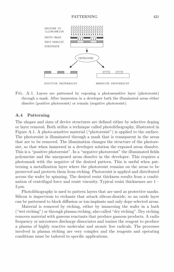
PATTERNING 421
DEVELOPER
NEGATIVE PHOTORESISTPOSITIVE PHOTORESIST
UNIFORM UVILLUMINATION
PHOTO-MASK
PHOT ORESIST
SUBSTRATE
Fig. A.1. Layers are patterned by exposing a photosensitive layer (photoresist)
through a mask. After immersion in a developer bath the illuminated areas either
dissolve (positive photoresist) or remain (negative photoresist).
A.4 Patterning
The shapes and sizes of device structures are defined either by selective dopingor layer removal. Both utilize a technique called photolithography, illustrated inFigure A.1. A photo-sensitive material (“photoresist”) is applied to the surface.The photoresist is illuminated through a mask that is transparent in the areasthat are to be removed. The illumination changes the structure of the photore-sist, so that when immersed in a developer solution the exposed areas dissolve.This is a “positive photoresist”. In a “negative photoresist” the illuminated fieldspolymerize and the unexposed areas dissolve in the developer. This requires aphotomask with the negative of the desired pattern. This is useful when pat-terning a metallization layer where the photoresist remains on the areas to bepreserved and protects them from etching. Photoresist is applied and distributedacross the wafer by spinning. The desired resist thickness results from a combi-nation of centrifugal force and resist viscosity. Typical resist thicknesses are 1 –2 µm.
Photolithography is used to pattern layers that are used as protective masks.Silicon is impervious to etchants that attack silicon-dioxide, so an oxide layercan be patterned to block diffusion or ion-implants and only dope selected areas.
Material is removed by etching, either by immersing the wafer in a bath(“wet etching”) or through plasma etching, also called “dry etching”. Dry etchingremoves material with gaseous reactants that produce gaseous products. A radiofrequency or microwave discharge dissociates and ionizes the reagent to producea plasma of highly reactive molecular and atomic free radicals. The processesinvolved in plasma etching are very complex and the reagents and operatingconditions must be tailored to specific applications.
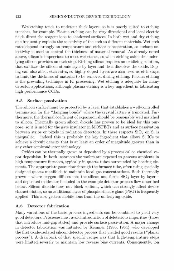
422 SEMICONDUCTOR DEVICE TECHNOLOGY
Wet etching tends to undercut thick layers, so it is poorly suited to etchingtrenches, for example. Plasma etching can be very directional and local electricfields direct the reagent ions to shadowed surfaces. In both wet and dry etchingone frequently exploits the selectivity of the etch to different materials. Wet etchrates depend strongly on temperature and etchant concentration, so etchant se-lectivity is used to control the thickness of material removal. As already notedabove, silicon is impervious to most wet etches, so when etching oxide the under-lying silicon provides an etch stop. Etching silicon requires an oxidizing solution,that oxidizes the silicon atomic layer by layer and then dissolves the oxide. Dop-ing can also affect etch rates, so highly doped layers are also used as etch stopsto limit the thickness of material to be removed during etching. Plasma etchingis the prevailing technique in IC processing. Wet etching is adequate for manydetector applications, although plasma etching is a key ingredient in fabricatinghigh performance CCDs.
A.5 Surface passivation
The silicon surface must be protected by a layer that establishes a well-controlledtermination for the “dangling bonds” where the crystal lattice is truncated. Fur-thermore, the thermal coefficient of expansion should be reasonably well matchedto silicon. Thermally grown silicon dioxide has proven to be ideal for this pur-pose, so it is used for the gate insulator in MOSFETs and as surface passivationbetween strips or pixels in radiation detectors. In these respects SiO2 on Si isunequalled – indeed this is probably the key ingredient that allows Si ICs toachieve a circuit density that is at least an order of magnitude greater than inany other semiconductor technology.
Oxides can be thermally grown or deposited by a process called chemical va-por deposition. In both instances the wafers are exposed to gaseous ambients inhigh temperature furnaces, typically in quartz tubes surrounded by heating ele-ments. The appropriate gases flow through the furnace tube, often using speciallydesigned quartz manifolds to maintain local gas concentrations. Both thermallygrown – where oxygen diffuses into the silicon and forms SiO2 layer by layer –and deposited oxides are included in the example detector process flow describedbelow. Silicon dioxide does not block sodium, which can strongly affect devicecharacteristics, so an additional layer of phosphosilicate glass (PSG) is frequentlyapplied. This also getters mobile ions from the underlying oxide.
A.6 Detector fabrication
Many variations of the basic process ingredients can be combined to yield verygood detectors. Processes must avoid introduction of deleterious impurities (thosethat introduce mid-gap states) and provide surface passivation. A major changein detector fabrication was initiated by Kemmer (1980, 1984), who developedthe first oxide-isolated silicon detector process that yielded good results (“planarprocess”). A drawback of that specific recipe was that high-temperature stepswere limited severely to maintain low reverse bias currents. Consequently, ion
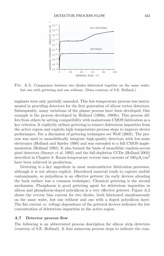
DETECTOR PROCESS FLOW 423
REVERSE BIAS (V)
0 20 40 60 80 10010
10
10
10
10
10
10
10
10
10
-12
-11
-10
-9
-8
-7
-6
-5
-4
-3
NOT GETTERED
GETTEREDREVERSECURRENT
DENSITY(A/cm
)2
Fig. A.2. Comparison between two diodes fabricated together on the same wafer,
but one with gettering and one without. (Data courtesy of S.E. Holland.)
implants were only partially annealed. This low-temperature process was instru-mental in providing detectors for the first generation of silicon vertex detectors.Subsequently, many variations of the planar process have been developed. Oneexample is the process developed by Holland (1989a, 1989b). This process dif-fers from others by setting compatibility with mainstream CMOS fabrication as akey criterion. It explicitly utilizes gettering to remove deleterious impurities fromthe active region and exploits high temperature process steps to improve deviceperformance. For a discussion of gettering techniques see Wolf (2002). The pro-cess was used to monolithically integrate high-quality detectors with low-noiseelectronics (Holland and Spieler 1990) and was extended to a full CMOS imple-mentation (Holland 1992). It also formed the basis of monolithic random-accesspixel detectors (Snoeys et al. 1992) and the full-depletion CCDs (Holland 2003)described in Chapter 8. Room-temperature reverse bias currents of 100 pA/cm2
have been achieved in production.Gettering is a key ingredient in most semiconductor fabrication processes,
although it is not always explicit. Disordered material tends to capture mobilecontaminants, so polysilicon is an effective getterer (in early devices abradingthe back surface was a common technique). Chemical gettering is the secondmechanism. Phosphorus is good gettering agent for deleterious impurities insilicon and phosphorus-doped polysilicon is a very effective getterer. Figure A.2shows the reverse bias current for two diodes, both fabricated simultaneouslyon the same wafer, but one without and one with a doped polysilicon layer.The flat current vs. voltage dependence of the gettered devices indicates the lowconcentration of deleterious impurities in the active region.
A.7 Detector process flow
The following is an abbreviated process description for silicon strip detectors(courtesy of S.E. Holland). It lists numerous process steps to indicate the com-
424 SEMICONDUCTOR DEVICE TECHNOLOGY
a) DEPOSITP-DOPED POLY-SiBACKSIDE CONT ACT
b) BACK CONTACT PROTECTEDBY Si-NITRIDE CAPPING LAYER
c)THERMAL OXIDATION OFTOP SURFACE
d) OPEN WINDOW FOR pELECTRODE
e) B-DOPINGTO FORM pELECTRODE
+ + f)ALUMINUM METALLIZATIONFOR FRONT CONTACT
i)ALUMINUM METALLIZATIONFOR BACK CONTACT
h) ETCH FRONT CONTACTg) PHOTORESIST MASKFOR FRONT CONTACT
Fig. A.3. Some key steps in a detector fabrication process. See text for details.
plexity involved in fabricating rather simple devices. Intermediate steps areshown in Figure A.3. Various process ingredients interact in complex ways, no-tably doping and thermal cycles. Detailed process simulators are available toevaluate the cumulative effect of all process steps on the final device.
1. First the entire wafer is coated with a doped polysilicon layer, which is thenremoved from the front of the wafer. On the backside the doped polysiliconremains as both a gettering layer and the ohmic electrode of the diode.
(a) Deposition of ∼ 0.5 µm low-temperature oxide (LTO) ∼ 1 hr at 400 C.
(b) Apply photoresist to wafer frontside.(c) Etch backside oxide. This leaves a clean silicon surface.
(d) Deposit ∼ 1.2 µm phosphorus-doped polysilicon (Figure A.3a).
(e) Deposit silicon nitride to protect wafer backside. This acts as a back-side capping layer during subsequent processing.
(f) Dry etch frontside nitride.
(g) Dry etch frontside polysilicon.
(h) Wet etch LTO (Figure A.3b).
2. Grow thermal oxide (steam, 4 hrs at 900 C to form a 400nm thick oxide).This will ultimately remain as the interstrip passivation (Figure A.3c).
3. Deposit photoresist.
4. Expose photoresist through mask with strip pattern, develop.
5. Etch exposed oxide (Figure A.3d).
6. Introduce p-dopant, typically boron, to form strip electrodes (Figure A.3e).Two methods are possible:
(a) thermal diffusion: expose to B203 source for 30min at 900 C.(b) ion implantation: 30 keV B ions at a dose of 2 · 1015 cm2.

DETECTOR PROCESS FLOW 425
7. Drive-in and thermal anneal of implant, combined with oxidation: 40minat 900 C in steam followed by 80min at 900 C in N2.
8. Deposit 500nm aluminum-silicon alloy for contacts (Figure A.3f).
9. Spin on photoresist.
10. Expose through a mask to form strip metallization and bonding pads andthen develop resist (Figure A.3g).
11. Etch metal (Figure A.3h).
12. Coat front side with photoresist.
13. Etch away backside nitride capping layer.
14. Deposit 100nm aluminum on back side to form ohmic contact (FigureA.3i).
15. Forming gas anneal to reduce density of interface states at Si–SiO2 inter-face: 20min at 400 C in 80% H2 + 20% N2.
Additional intermediate steps are necessary: Wafers must be cleaned prior toeach furnace step (except the post-metallization anneal). “DI water” refers tohigh purity water with sub-ppb contamination levels. With regard to contamina-tion water is one of the most critical process ingredients, as wafers are exposedto many more water molecules than air. An “HF etch” immerses the wafer indiluted hydrofluoric acid to strip oxide off of the wafer surface.
1. Immerse in 5:1:1 solution of H2O : H2S04 : H202 at 120 C.
2. HF etch.
3. Rinse in DI water.
4. Immerse in 5:1:1 solution of H2O : NH4OH : H202 at 65 C.
5. Dilute HF etch.
6. Rinse in DI water.
7. Immerse in 5:1:1 solution of H2O : HCl : H202 at 65C.
8. Rinse in DI water.
The overall process takes several weeks. Processing typically proceeds in cleanrooms of class 100 or better, i.e. with fewer than 100 particles > 0.5 µm in sizeper cubic foot. For comparison, hospital operating rooms are class ∼ 105 and the“normal” air in a big city has ∼ 108 particles per cubic foot. Wafers are typicallyprocessed in batches of 25 – 50. Handling of individual wafers is minimized byusing wafer holders, for example to immerse multiple wafers at once in a bath.Semirobotic systems automate the application of photoresist and baking, whichmust be well-controlled at small feature sizes. Furnaces are computer controlledto ensure that temperature ramping and gas flows follow the required recipe.Dedicated furnace tubes are used and gas lines are purged before and after eachprocess step to prevent cross-contamination.
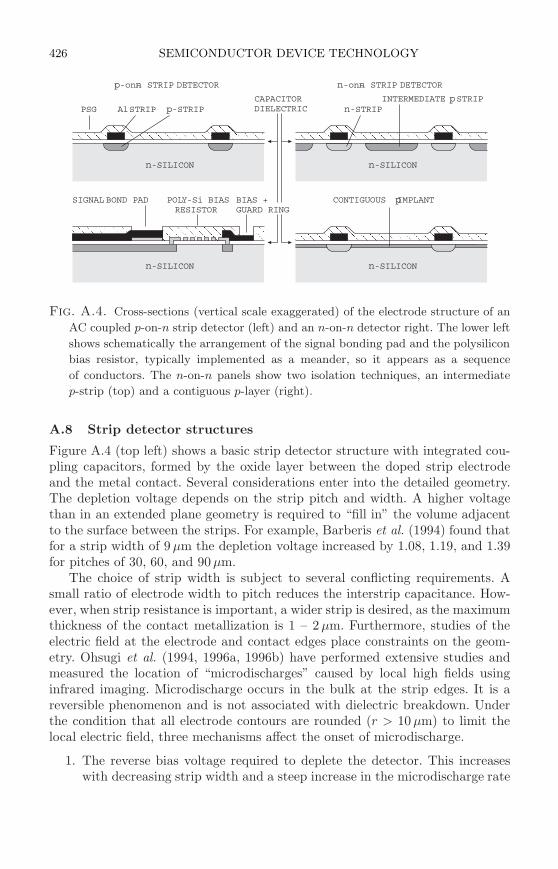
426 SEMICONDUCTOR DEVICE TECHNOLOGY
p n-on- STRIP DETECTOR n n-on- STRIP DETECTOR
SIGNAL BOND PAD POLY-Si BIASRESISTOR
BIAS +GUARD RING
p-STRIP n-STRIP
n-SILICON n-SILICON
n-SILICON n-SILICON
AlSTRIPINTERMEDIATE STRIPp
CONTIGUOUS IMPLANTp
PSGCAPACITORDIELECTRIC
Fig. A.4. Cross-sections (vertical scale exaggerated) of the electrode structure of an
AC coupled p-on-n strip detector (left) and an n-on-n detector right. The lower left
shows schematically the arrangement of the signal bonding pad and the polysilicon
bias resistor, typically implemented as a meander, so it appears as a sequence
of conductors. The n-on-n panels show two isolation techniques, an intermediate
p-strip (top) and a contiguous p-layer (right).
A.8 Strip detector structures
Figure A.4 (top left) shows a basic strip detector structure with integrated cou-pling capacitors, formed by the oxide layer between the doped strip electrodeand the metal contact. Several considerations enter into the detailed geometry.The depletion voltage depends on the strip pitch and width. A higher voltagethan in an extended plane geometry is required to “fill in” the volume adjacentto the surface between the strips. For example, Barberis et al. (1994) found thatfor a strip width of 9 µm the depletion voltage increased by 1.08, 1.19, and 1.39for pitches of 30, 60, and 90µm.
The choice of strip width is subject to several conflicting requirements. Asmall ratio of electrode width to pitch reduces the interstrip capacitance. How-ever, when strip resistance is important, a wider strip is desired, as the maximumthickness of the contact metallization is 1 – 2µm. Furthermore, studies of theelectric field at the electrode and contact edges place constraints on the geom-etry. Ohsugi et al. (1994, 1996a, 1996b) have performed extensive studies andmeasured the location of “microdischarges” caused by local high fields usinginfrared imaging. Microdischarge occurs in the bulk at the strip edges. It is areversible phenomenon and is not associated with dielectric breakdown. Underthe condition that all electrode contours are rounded (r > 10 µm) to limit thelocal electric field, three mechanisms affect the onset of microdischarge.
1. The reverse bias voltage required to deplete the detector. This increaseswith decreasing strip width and a steep increase in the microdischarge rate
STRIP DETECTOR STRUCTURES 427
is observed for ratios of strip width to pitch w/p ≥ 0.2 (Ohsugi et al. 1999).A deep diffusion is beneficial as it increases the radius of curvature.
2. The potential across the integrated coupling capacitor. When operatedwith the full bias voltage across the capacitor this is the dominant fieldaround the strip, so the total field is highest at the junction side. However,this is also significant at the ohmic side when the detector is operatedwell beyond depletion. The field increases steeply when the contact widthexceeds the implant width. The contact edge should be kept 2 – 3µm insidethe strip electrode.
3. Charge trapped in the dielectric oxide or at the oxide–silicon interface.This contribution to the field is exacerbated at the p-side, as on the n-sideit is partially cancelled by the field across the capacitor.
Moving the high-field regions from the bulk into the dielectric is advanta-geous, as the breakdown field in the oxide is much greater than in the bulk(103 V/µm vs. 30 V/µm). This can be accomplished by thickening the oxide be-yond the implant edges and extending the metallization to provide an overhangbeyond the implant width (Ohsugi et al. 1996a, Passeri et al. 2000). Another limitto the maximum bias voltage is determined by the guard ring structure, whichmust ensure that the potential is appropriately graded to avoid high fields at theedge of the sensor. Multiple guard rings are often used to control the potentialgradient (for an example see Andricek et al. 2000), although other techniquescan be applied (Ohsugi et al. 1999).
The design of optimum structures for double-sided detectors is discussed byOhsugi et al. (1999). Passeri et al. (2001) discuss the interstrip capacitance vs.metal overhang. Figure A.4 (left) shows a strip detector with integrated couplingcapacitors. For simplicity, this does not include the metal overhang. Since thedielectric is deposited, it is subject to pinholes depending on the quality of the un-derlying surface. This limits the breakdown voltage and overall reliability of thecapacitor. Multilayer dielectrics are effective against pinholes. Silicon-nitride hasa higher dielectric constant and breakdown field, so oxide-nitride layers are com-monly used (Ohsugi et al. 1996a). Holland (1995) discusses oxide-nitride-oxidelayers and equivalent coupling circuits. Nevertheless, the integrated capacitorsoften develop defects, so some detectors “float” their readout electronics at thedetector bias level to maintain minimal voltage across the capacitors. Their solepurpose then is to block the detector bias current from flowing into the amplifierinput.
With AC coupling each strip requires a DC return path, which is best imple-mented with resistors, implemented as narrow strip meanders of lightly dopedpolysilicon. These are placed at the ends of the strips between the strip elec-trodes and the guard ring, which isolates the detector’s active area from thewafer saw cut. A common bias connection feeds all strips. This is shown in thelower left cross-section of Figure A.4. Some detector designs utilize MOSFETstructures to bias the individual strips (often called FOXFET biasing), but as
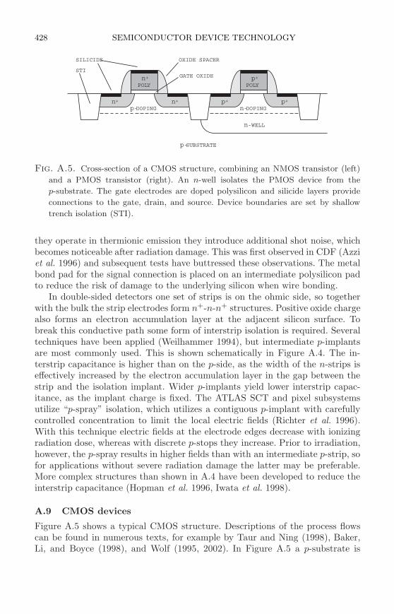
428 SEMICONDUCTOR DEVICE TECHNOLOGY
OXIDE SPACERSILICIDE
n
n p
n p p+
+ +
+ + +
n-WELL
DOPINGn-DOPINGp-
SUBSTRATEp-
POLY POLY
STIGATE OXIDE
Fig. A.5. Cross-section of a CMOS structure, combining an NMOS transistor (left)
and a PMOS transistor (right). An n-well isolates the PMOS device from the
p-substrate. The gate electrodes are doped polysilicon and silicide layers provide
connections to the gate, drain, and source. Device boundaries are set by shallow
trench isolation (STI).
they operate in thermionic emission they introduce additional shot noise, whichbecomes noticeable after radiation damage. This was first observed in CDF (Azziet al. 1996) and subsequent tests have buttressed these observations. The metalbond pad for the signal connection is placed on an intermediate polysilicon padto reduce the risk of damage to the underlying silicon when wire bonding.
In double-sided detectors one set of strips is on the ohmic side, so togetherwith the bulk the strip electrodes form n+-n-n+ structures. Positive oxide chargealso forms an electron accumulation layer at the adjacent silicon surface. Tobreak this conductive path some form of interstrip isolation is required. Severaltechniques have been applied (Weilhammer 1994), but intermediate p-implantsare most commonly used. This is shown schematically in Figure A.4. The in-terstrip capacitance is higher than on the p-side, as the width of the n-strips iseffectively increased by the electron accumulation layer in the gap between thestrip and the isolation implant. Wider p-implants yield lower interstrip capac-itance, as the implant charge is fixed. The ATLAS SCT and pixel subsystemsutilize “p-spray” isolation, which utilizes a contiguous p-implant with carefullycontrolled concentration to limit the local electric fields (Richter et al. 1996).With this technique electric fields at the electrode edges decrease with ionizingradiation dose, whereas with discrete p-stops they increase. Prior to irradiation,however, the p-spray results in higher fields than with an intermediate p-strip, sofor applications without severe radiation damage the latter may be preferable.More complex structures than shown in A.4 have been developed to reduce theinterstrip capacitance (Hopman et al. 1996, Iwata et al. 1998).
A.9 CMOS devices
Figure A.5 shows a typical CMOS structure. Descriptions of the process flowscan be found in numerous texts, for example by Taur and Ning (1998), Baker,Li, and Boyce (1998), and Wolf (1995, 2002). In Figure A.5 a p-substrate is
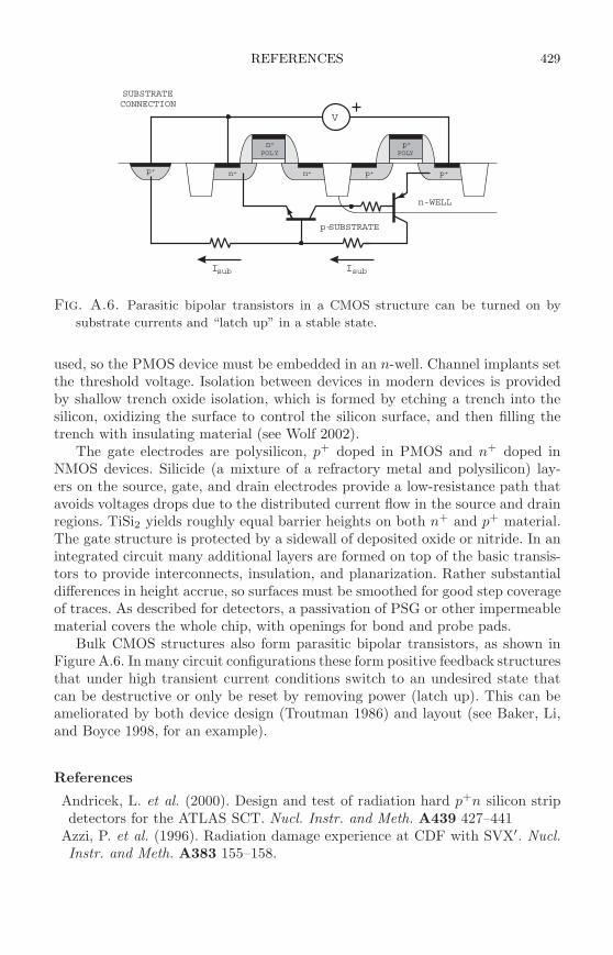
REFERENCES 429
n
n p
n p p+
+ +
+ + +
n-WELL
SUBSTRATEp-
POLY POLY
p+
SUBSTRATECONNECTION
V
I Isub sub
Fig. A.6. Parasitic bipolar transistors in a CMOS structure can be turned on by
substrate currents and “latch up” in a stable state.
used, so the PMOS device must be embedded in an n-well. Channel implants setthe threshold voltage. Isolation between devices in modern devices is providedby shallow trench oxide isolation, which is formed by etching a trench into thesilicon, oxidizing the surface to control the silicon surface, and then filling thetrench with insulating material (see Wolf 2002).
The gate electrodes are polysilicon, p+ doped in PMOS and n+ doped inNMOS devices. Silicide (a mixture of a refractory metal and polysilicon) lay-ers on the source, gate, and drain electrodes provide a low-resistance path thatavoids voltages drops due to the distributed current flow in the source and drainregions. TiSi2 yields roughly equal barrier heights on both n+ and p+ material.The gate structure is protected by a sidewall of deposited oxide or nitride. In anintegrated circuit many additional layers are formed on top of the basic transis-tors to provide interconnects, insulation, and planarization. Rather substantialdifferences in height accrue, so surfaces must be smoothed for good step coverageof traces. As described for detectors, a passivation of PSG or other impermeablematerial covers the whole chip, with openings for bond and probe pads.
Bulk CMOS structures also form parasitic bipolar transistors, as shown inFigure A.6. In many circuit configurations these form positive feedback structuresthat under high transient current conditions switch to an undesired state thatcan be destructive or only be reset by removing power (latch up). This can beameliorated by both device design (Troutman 1986) and layout (see Baker, Li,and Boyce 1998, for an example).
References
Andricek, L. et al. (2000). Design and test of radiation hard p+n silicon stripdetectors for the ATLAS SCT. Nucl. Instr. and Meth. A439 427–441
Azzi, P. et al. (1996). Radiation damage experience at CDF with SVX′. Nucl.Instr. and Meth. A383 155–158.
430 SEMICONDUCTOR DEVICE TECHNOLOGY
Baker, R.J., Li, H.W., and Boyce, D.E. (1998). CMOS Circuit Design, Layout,and Simulation. IEEE Press, New York. ISBN 0-7803-3416-7,TK7871.99.M44B35 1997
Fair, R.B. (1981). Concentration profiles of diffused dopants in silicon. in Im-purity Doping Processes in Silicon, F.F.F. Wang (ed). North Holland, Ams-terdam. ISBN 0-444-86095-9, TK7871.85.I48
Holland, S.E. (1989a). An IC-compatible detector process IEEE Trans. Nucl.Sci. NS-36/1 (1989) 283–288
Holland, S.E. (1989b). Fabrication of detectors and transistors on high-resistivitysilicon. Nucl. Instr. and Meth. A275 (1989) 537–541
Holland, S. and Spieler, H. (1990). A monolithically integrated detector–pre-amplifier on high-resistivity silicon. IEEE Trans. Nucl. Sci. NS-37/2 (1990)463–468
Holland, S. (1992). Properties of CMOS devices and circuits fabricated on high-resistivity, detector-grade silicon.IEEE Trans. Nucl. Sci. NS-39/4 (1992) 809–813
Holland, S. (1995). An oxide-nitride-oxide capacitor dielectric film for siliconstrip detectors. IEEE Trans. Nucl. Sci. NS-42/4 423–427
Holland, S.E. et al. (2003). Fully depleted, back-illuminated charge-coupleddevices fabricated on high-resistivity silicon. IEEE Trans. Electron. Dev. ED-50/1 (2003) 225–238 and LBNL-49992
Hopman, P.I. et al. (1996). Optimization of silicon microstrip detector designfor CLEO III. Nucl. Instr. and Meth. A383 (1996) 98–103
Iwata, Y. et al. (1998). Optimal p-stop pattern for the n-side strip isolation ofsilicon microstrip detectors. IEEE Trans. Nucl. Sci. NS-45/3 (1998) 303–309
Kemmer, J. (1980). Fabrication of low noise silicon radiation detectors by theplanar process. Nucl. Instr. and Meth. 169 (1980) 499–502
Kemmer, J. (1984). Improvement of detector fabrication by the planar process.Nucl. Instr. and Meth. 226 (1984) 89–93
Lutz, G. (1999). Semiconductor Radiation Detectors. Springer Verlag, Berlin,1999. ISBN 3-5406-4859-3
Nishi, Y. and Doering, R. (eds) (2000). Handbook of Semiconductor Manufac-turing Technology. Marcel Dekker, New York, 2000. ISBN 0-8247-8783-8
Ohsugi, T. et al. (1994). Microdischarges of AC-coupled silicon strip sensors.Nucl. Instr. and Meth. A342 (1994) 22–26
Ohsugi, T. et al. (1996a). Micro-discharge at strip edge of silicon microstripsensors Nucl. Instr. and Meth. A383 (1996) 116–122
Ohsugi, T. et al. (1996b). Micro-discharge noise and radiation damage of siliconmicrostrip sensors Nucl. Instr. and Meth. A383 (1996) 166–173
Ohsugi, T. et al. (1999). Design optimization of radiation-hard, double-sided,double-metal, AC-coupled silicon sensors. Nucl. Instr. and Meth. A436 (1999)272–280
Passeri, D. et al. (2000). Optimization of overhanging-metal microstrip detec-tors: test and simulation IEEE Trans. Nucl. Sci. NS-48/3 (2001) 249–253
REFERENCES 431
Passeri, D. et al. (2001). Physical modeling of silicon microstrip detectors: in-fluence of the electrode geometry on critical electric fields. IEEE Trans. Nucl.Sci. NS-47/4 (2000) 1468–1473
Richter, R.H. et al. (1996). Strip detector design for ATLAS and HERA-Busing two-dimensional device simulation. Nucl. Instr. and Meth. A377 (1996)412–421
Ryssel, H. and Glawischnig, H. (eds) (1982). Ion Implantation Techniques.Springer Verlag, Berlin, 1982. ISBN 3-540-11878-0
Sze, S.M. (1981). Physics of Semiconductor Devices. Wiley, New York 1981.ISBN 0-471-05661-8, TK7871.85.S988 1981
Snoeys, W. et al. (1992). A new integrated pixel detector for high energy physicsIEEE Trans. Nucl. Sci. NS-39/5 (1992) 1263–1269
Taur, Y. and Ning, T.H. (1998). Fundamentals of Modern VLSI Devices. Cam-bridge University Press, Cambridge. ISBN 0-521-55056-6, TK7871.99.M44T38
Troutman, R.R. (1986). Latch-up in CMOS Technology. Kluwer, BostonWeilhammer, P. (1994). Double-sided Si strip sensors for LEP vertex detectors.Nucl. Instr. and Meth. A342 (1994) 1–15
Wolf, S. (1995). Silicon Processing for the VLSI Era, Volume 3 – The SubmicronMOSFET. Lattice Press, Sunset Beach, ISBN 0-961672-5-3
Wolf, S. (2002). Silicon Processing for the VLSI Era, Volume 4 – Deep-SubmicronProcess Technology. Lattice Press, Sunset Beach, ISBN 0-9616721-7-X
APPENDIX B
PHASORS AND COMPLEX ALGEBRA IN ELECTRICAL
CIRCUITS
Consider the RLC circuit shown in Figure B.1. The total voltage developedacross the circuit
V = VR + VL + VC
V = IR + LdI
dt+
Q
CdV
dt=
dI
dtR + L
d2I
dt2+
I
C. (B.1)
The desired result can be found by solving the differential equation, but sincesimilar problems occur repeatedly, simpler techniques have been developed. Ifwe write V (t) and I(t) in the form
V (t) = V0eiωt
I(t) = I0ei(ωt+ϕ) , (B.2)
then eqn B.1 becomes
iωV0eiωt = iωRI0e
i(ωt−ϕ) − ω2LI0ei(ωt−ϕ) +
1
CI0e
i(ωt−ϕ)
V0
I0eiϕ = R + iωL − i
1
ωC. (B.3)
It( )
V t( )
C
L
R V
V
V
R
L
C
Fig. B.1. A resistor, inductor, and capacitor connected in series and driven by a
voltage source.
432
PHASORS AND COMPLEX ALGEBRA IN ELECTRICAL CIRCUITS 433
Re
Im
R
Z
i i L C- /
- /i C
iL
Fig. B.2. The series RLC circuit is represented in the complex plane by “phasors”
that characterize the magnitude and phase of the impedance.
Thus, we can express the total impedance Z ≡ (V0/I0)eiϕ of the circuit as a com-
plex number with the magnitude |Z| = V0/I0 and phase ϕ. In this representationthe equivalent resistances (reactances) of L and C are imaginary numbers.
Plotted in the complex plane (Figure B.2) the components on the right side ofeqn B.3 are represented as “phasors”, whose magnitude and phase characterizethe impedance. Relative to VR, the voltage across the inductor VL is shifted inphase by +90. The voltage across the capacitor VC is shifted in phase by −90.
The total impedance has the magnitude
|Z| =
√
[Re(Z)]2 + [Im(Z)]2 =
√
R2 +
(
ωL − 1
ωC
)2
(B.4)
and phase
tanϕ =Im(Z)
Re(Z)=
ωL − 1
ωCR
. (B.5)
From eqn B.4 one sees immediately that the impedance Z assumes a minimumat
ω =1√LC
, (B.6)
the resonant frequency of the tuned circuit. The impedance vs. frequency yieldsthe resonance curve. At resonance the phase ϕ becomes zero.
At frequencies above resonance the inductive reactance dominates (as ap-parent in Figure B.2) and the asymptotic phase is +90. Below resonance thecapacitive reactance dominates and the asymptotic phase is −90. This repre-sentation can be used for any element that introduces a phase shift, e.g. anamplifier. A phase shift of +90 appears as +i, −90 as −i.
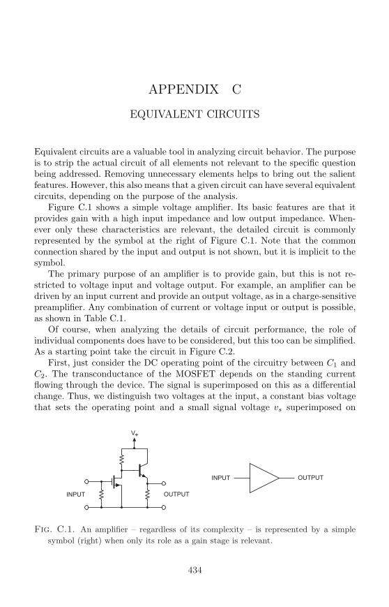
APPENDIX C
EQUIVALENT CIRCUITS
Equivalent circuits are a valuable tool in analyzing circuit behavior. The purposeis to strip the actual circuit of all elements not relevant to the specific questionbeing addressed. Removing unnecessary elements helps to bring out the salientfeatures. However, this also means that a given circuit can have several equivalentcircuits, depending on the purpose of the analysis.
Figure C.1 shows a simple voltage amplifier. Its basic features are that itprovides gain with a high input impedance and low output impedance. When-ever only these characteristics are relevant, the detailed circuit is commonlyrepresented by the symbol at the right of Figure C.1. Note that the commonconnection shared by the input and output is not shown, but it is implicit to thesymbol.
The primary purpose of an amplifier is to provide gain, but this is not re-stricted to voltage input and voltage output. For example, an amplifier can bedriven by an input current and provide an output voltage, as in a charge-sensitivepreamplifier. Any combination of current or voltage input or output is possible,as shown in Table C.1.
Of course, when analyzing the details of circuit performance, the role ofindividual components does have to be considered, but this too can be simplified.As a starting point take the circuit in Figure C.2.
First, just consider the DC operating point of the circuitry between C1 andC2. The transconductance of the MOSFET depends on the standing currentflowing through the device. The signal is superimposed on this as a differentialchange. Thus, we distinguish two voltages at the input, a constant bias voltagethat sets the operating point and a small signal voltage vs superimposed on
V+
INPUT
INPUT
OUTPUT
OUTPUT
Fig. C.1. An amplifier – regardless of its complexity – is represented by a simple
symbol (right) when only its role as a gain stage is relevant.
434
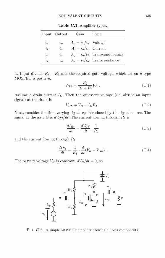
EQUIVALENT CIRCUITS 435
Table C.1 Amplifier types.
Input Output Gain Type
vi vo Av = vo/vi Voltage
ii io Ai = io/ii Current
vi io Ag = io/vi Transconductance
ii vo Ar = vi/io Transresistance
it. Input divider R1 − R2 sets the required gate voltage, which for an n-typeMOSFET is positive,
VGS =R2
R1 + R2VB . (C.1)
Assume a drain current ID . Then the quiescent voltage (i.e. absent an inputsignal) at the drain is
VDS = VB − IDR3 . (C.2)
Next, consider the time-varying signal vS introduced by the signal source. Thesignal at the gate G is dVGS/dt. The current flowing through R2 is
dIR2
dt=
dVGS
dt· 1
R2(C.3)
and the current flowing through R1
dIR1
dt=
1
R1· d
dt(VB − VGS) . (C.4)
The battery voltage VB is constant, dVB/dt = 0, so
R
RR
R
V
C
C
R
v
VV
S
1
3
B
1
2
2
s
GSDS
G D
S
Fig. C.2. A simple MOSFET amplifier showing all bias components.
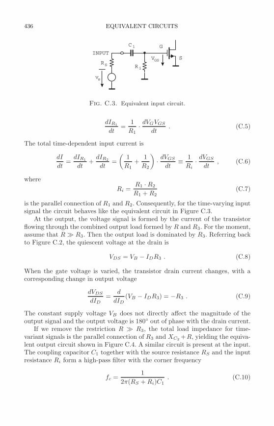
436 EQUIVALENT CIRCUITS
R
C
R
VS
1
i
GS
G
SINPUT
vs
Fig. C.3. Equivalent input circuit.
dIR1
dt=
1
R1· dVGVGS
dt. (C.5)
The total time-dependent input current is
dI
dt=
dIR1
dt+
dIR2
dt=
(
1
R1+
1
R2
)
· dVGS
dt≡ 1
Ri· dVGS
dt, (C.6)
where
Ri =R1 · R2
R1 + R2(C.7)
is the parallel connection of R1 and R2. Consequently, for the time-varying inputsignal the circuit behaves like the equivalent circuit in Figure C.3.
At the output, the voltage signal is formed by the current of the transistorflowing through the combined output load formed by R and R3. For the moment,assume that R ≫ R3. Then the output load is dominated by R3. Referring backto Figure C.2, the quiescent voltage at the drain is
VDS = VB − IDR3 . (C.8)
When the gate voltage is varied, the transistor drain current changes, with acorresponding change in output voltage
dVDS
dID=
d
dID(VB − IDR3) = −R3 . (C.9)
The constant supply voltage VB does not directly affect the magnitude of theoutput signal and the output voltage is 180 out of phase with the drain current.
If we remove the restriction R ≫ R3, the total load impedance for time-variant signals is the parallel connection of R3 and XC2
+R, yielding the equiva-lent output circuit shown in Figure C.4. A similar circuit is present at the input.The coupling capacitor C1 together with the source resistance RS and the inputresistance Ri form a high-pass filter with the corner frequency
fc =1
2π(RS + Ri)C1. (C.10)
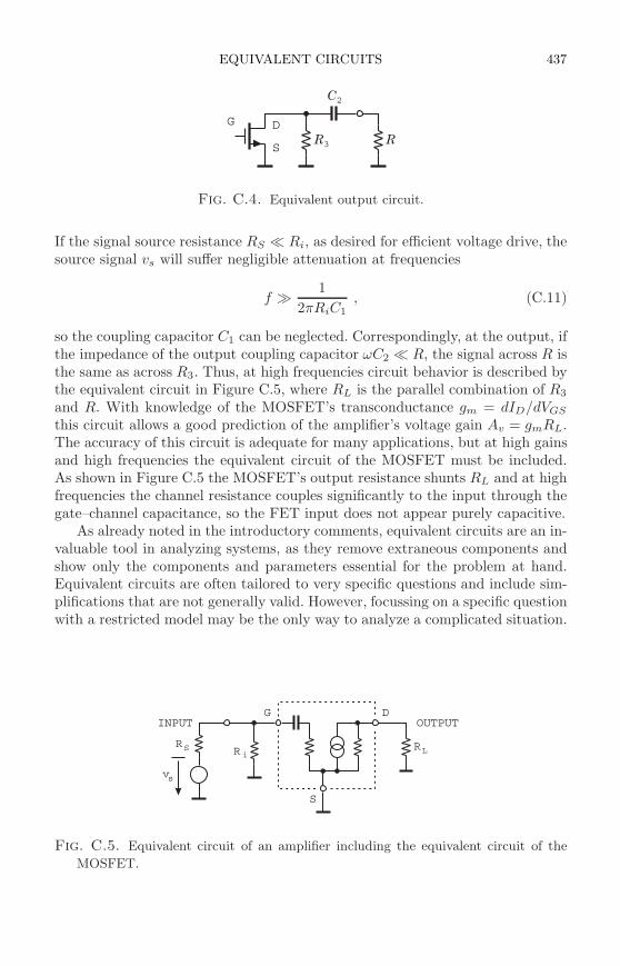
EQUIVALENT CIRCUITS 437
R R
C
3
2
G D
S
Fig. C.4. Equivalent output circuit.
If the signal source resistance RS ≪ Ri, as desired for efficient voltage drive, thesource signal vs will suffer negligible attenuation at frequencies
f ≫ 1
2πRiC1, (C.11)
so the coupling capacitor C1 can be neglected. Correspondingly, at the output, ifthe impedance of the output coupling capacitor ωC2 ≪ R, the signal across R isthe same as across R3. Thus, at high frequencies circuit behavior is described bythe equivalent circuit in Figure C.5, where RL is the parallel combination of R3
and R. With knowledge of the MOSFET’s transconductance gm = dID/dVGS
this circuit allows a good prediction of the amplifier’s voltage gain Av = gmRL.The accuracy of this circuit is adequate for many applications, but at high gainsand high frequencies the equivalent circuit of the MOSFET must be included.As shown in Figure C.5 the MOSFET’s output resistance shunts RL and at highfrequencies the channel resistance couples significantly to the input through thegate–channel capacitance, so the FET input does not appear purely capacitive.
As already noted in the introductory comments, equivalent circuits are an in-valuable tool in analyzing systems, as they remove extraneous components andshow only the components and parameters essential for the problem at hand.Equivalent circuits are often tailored to very specific questions and include sim-plifications that are not generally valid. However, focussing on a specific questionwith a restricted model may be the only way to analyze a complicated situation.
G D
S
RR RSi L
INPUT OUTPUT
vs
Fig. C.5. Equivalent circuit of an amplifier including the equivalent circuit of the
MOSFET.
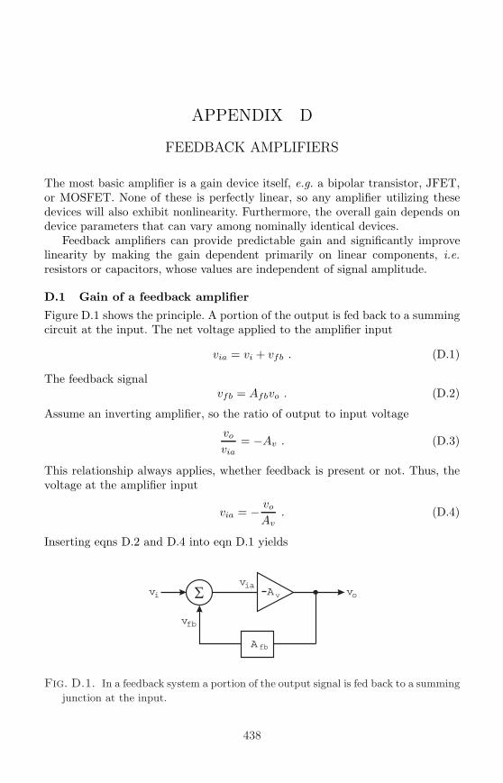
APPENDIX D
FEEDBACK AMPLIFIERS
The most basic amplifier is a gain device itself, e.g. a bipolar transistor, JFET,or MOSFET. None of these is perfectly linear, so any amplifier utilizing thesedevices will also exhibit nonlinearity. Furthermore, the overall gain depends ondevice parameters that can vary among nominally identical devices.
Feedback amplifiers can provide predictable gain and significantly improvelinearity by making the gain dependent primarily on linear components, i.e.resistors or capacitors, whose values are independent of signal amplitude.
D.1 Gain of a feedback amplifier
Figure D.1 shows the principle. A portion of the output is fed back to a summingcircuit at the input. The net voltage applied to the amplifier input
via = vi + vfb . (D.1)
The feedback signalvfb = Afbvo . (D.2)
Assume an inverting amplifier, so the ratio of output to input voltage
vo
via= −Av . (D.3)
This relationship always applies, whether feedback is present or not. Thus, thevoltage at the amplifier input
via = − vo
Av. (D.4)
Inserting eqns D.2 and D.4 into eqn D.1 yields
v
v
vv
A
i
fb
iaov
fb
A
Fig. D.1. In a feedback system a portion of the output signal is fed back to a summing
junction at the input.
438
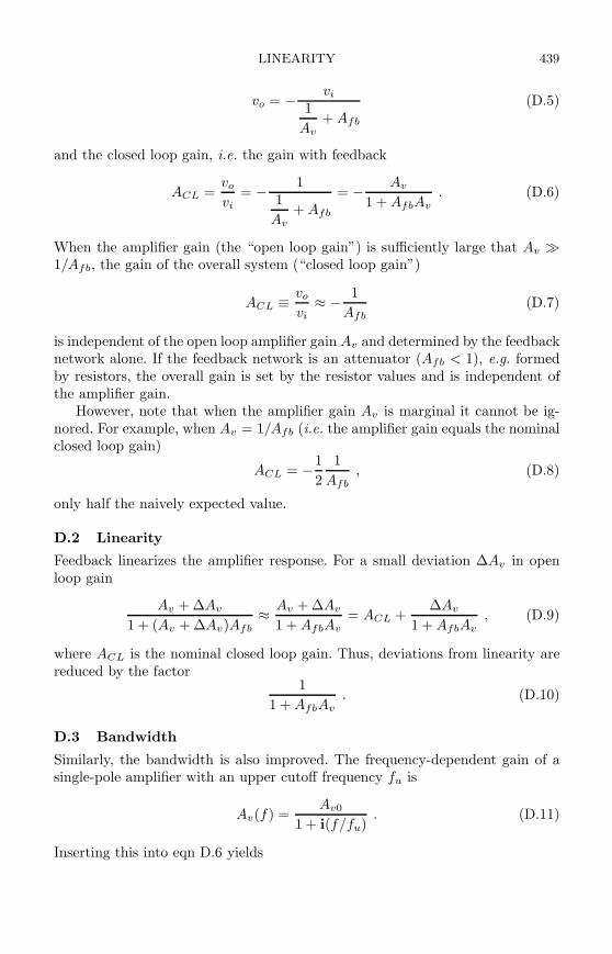
LINEARITY 439
vo = − vi
1
Av+ Afb
(D.5)
and the closed loop gain, i.e. the gain with feedback
ACL =vo
vi= − 1
1
Av+ Afb
= − Av
1 + AfbAv. (D.6)
When the amplifier gain (the “open loop gain”) is sufficiently large that Av ≫1/Afb, the gain of the overall system (“closed loop gain”)
ACL ≡ vo
vi≈ − 1
Afb(D.7)
is independent of the open loop amplifier gain Av and determined by the feedbacknetwork alone. If the feedback network is an attenuator (Afb < 1), e.g. formedby resistors, the overall gain is set by the resistor values and is independent ofthe amplifier gain.
However, note that when the amplifier gain Av is marginal it cannot be ig-nored. For example, when Av = 1/Afb (i.e. the amplifier gain equals the nominalclosed loop gain)
ACL = −1
2
1
Afb, (D.8)
only half the naively expected value.
D.2 Linearity
Feedback linearizes the amplifier response. For a small deviation ∆Av in openloop gain
Av + ∆Av
1 + (Av + ∆Av)Afb≈ Av + ∆Av
1 + AfbAv= ACL +
∆Av
1 + AfbAv, (D.9)
where ACL is the nominal closed loop gain. Thus, deviations from linearity arereduced by the factor
1
1 + AfbAv. (D.10)
D.3 Bandwidth
Similarly, the bandwidth is also improved. The frequency-dependent gain of asingle-pole amplifier with an upper cutoff frequency fu is
Av(f) =Av0
1 + i(f/fu). (D.11)
Inserting this into eqn D.6 yields
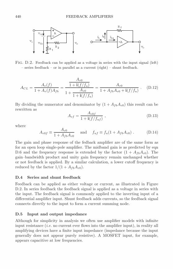
440 FEEDBACK AMPLIFIERS
RR
R
2
1
f
vi ii
vv
i
i iaf
o
o
via
vfb A
A
Fig. D.2. Feedback can be applied as a voltage in series with the input signal (left)
– series feedback – or in parallel as a current (right) – shunt feedback.
ACL =Av(f)
1 + Av(f)Afb=
Av0
1 + i(f/fu)
1 +Av0
1 + i(f/fu)
=Av0
1 + AfbAv0 + i(f/fu). (D.12)
By dividing the numerator and denominator by (1 + AfbAv0) this result can berewritten as
Avf =Av0f
1 + i(f/fuf ), (D.13)
where
Av0f ≡ Av0
1 + AfbAv0and fuf ≡ fu(1 + AfbAv0) . (D.14)
The gain and phase response of the fedback amplifier are of the same form asfor an open loop single-pole amplifier. The midband gain is as predicted by eqnD.6 and the frequency response is extended by the factor (1 + AfbAv0). Thegain–bandwidth product and unity gain frequency remain unchanged whetheror not feedback is applied. By a similar calculation, a lower cutoff frequency isreduced by the factor 1/(1 + AfbAv0).
D.4 Series and shunt feedback
Feedback can be applied as either voltage or current, as illustrated in FigureD.2. In series feedback the feedback signal is applied as a voltage in series withthe input. The feedback signal is commonly applied to the inverting input of adifferential amplifier input. Shunt feedback adds currents, so the feedback signalconnects directly to the input to form a current summing node.
D.5 Input and output impedance
Although for simplicity in analysis we often use amplifier models with infiniteinput resistance (i.e. no current ever flows into the amplifier input), in reality allamplifying devices have a finite input impedance (impedance because the inputgenerally does not appear purely resistive). A MOSFET input, for example,appears capacitive at low frequencies.
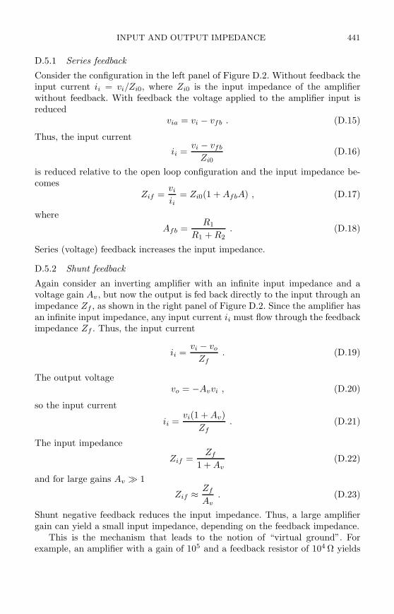
INPUT AND OUTPUT IMPEDANCE 441
D.5.1 Series feedback
Consider the configuration in the left panel of Figure D.2. Without feedback theinput current ii = vi/Zi0, where Zi0 is the input impedance of the amplifierwithout feedback. With feedback the voltage applied to the amplifier input isreduced
via = vi − vfb . (D.15)
Thus, the input current
ii =vi − vfb
Zi0(D.16)
is reduced relative to the open loop configuration and the input impedance be-comes
Zif =vi
ii= Zi0(1 + AfbA) , (D.17)
where
Afb =R1
R1 + R2. (D.18)
Series (voltage) feedback increases the input impedance.
D.5.2 Shunt feedback
Again consider an inverting amplifier with an infinite input impedance and avoltage gain Av , but now the output is fed back directly to the input through animpedance Zf , as shown in the right panel of Figure D.2. Since the amplifier hasan infinite input impedance, any input current ii must flow through the feedbackimpedance Zf . Thus, the input current
ii =vi − vo
Zf. (D.19)
The output voltagevo = −Avvi , (D.20)
so the input current
ii =vi(1 + Av)
Zf. (D.21)
The input impedance
Zif =Zf
1 + Av(D.22)
and for large gains Av ≫ 1
Zif ≈ Zf
Av. (D.23)
Shunt negative feedback reduces the input impedance. Thus, a large amplifiergain can yield a small input impedance, depending on the feedback impedance.
This is the mechanism that leads to the notion of “virtual ground”. Forexample, an amplifier with a gain of 105 and a feedback resistor of 104 Ω yields
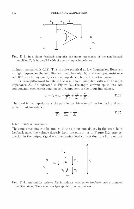
442 FEEDBACK AMPLIFIERS
Z
i i Z
i
a
i f f
a
vi
vo
Fig. D.3. In a shunt feedback amplifier the input impedance of the non-fedback
amplifier Za is in parallel with the active input impedance.
an input resistance is 0.1 Ω. This is quite practical at low frequencies. However,at high frequencies the amplifier gain may be only 100, and the input resistanceis 100 Ω, which may qualify as a low impedance, but not a virtual ground.
It is straightforward to extend the result to an amplifier with a finite inputimpedance Za. As indicated in Figure D.3 the input current splits into twocomponents, each corresponding to a component of the input impedance,
ii = if + ia =vi
Zif+
vi
Za≡ vi
Zi. (D.24)
The total input impedance is the parallel combination of the feedback and am-plifier input impedance
1
Zi=
1
Zif+
1
Za. (D.25)
D.5.3 Output impedance
The same reasoning can be applied to the output impedance. In this case shuntfeedback takes the voltage directly from the output, as in Figure D.2. Any re-duction in the output signal with increasing load current due to a finite output
V
V
V V
I
VR
BE
B
CE C
C
EE
Fig. D.4. An emitter resistor RE introduces local series feedback into a common
emitter stage. The same principle applies to other devices.
LOOP GAIN 443
impedance will also reduce the magnitude of the fedback signal, compensatingfor the output drop. This effectively reduces the output impedance to
Zof =Zo
1 + AfbAv. (D.26)
Conversely, series feedback will increase the output impedance. Figure D.4shows an example of local series feedback. The emitter resistor introduces avoltage drop into the input circuit that depends on the output current. If theoutput voltage sags because of the inherent output resistance of the device, thecurrent decreases, which in turn reduces the voltage drop across the emitterresistor and increases the base–emitter voltage to counteract the decrease inoutput current.
For a constant input voltage VB applied to the base, the collector voltage
VC = ICRE + VCE(VBE , IC) . (D.27)
The total differential
dVC = dICRE + dVBEdVCE
dVBE+ dIC
dVCE
dIC. (D.28)
Since dVBE = −dICRE and the output resistance of the transistor ro = dVCE/dIC ,the change in output voltage
dVC = dICRE − dICREdVCE
dVBE+ dICro . (D.29)
Using dIC/dVBE = gm and dVCE = −dICRE , the output resistance with feed-back becomes
rof ≡ dVC
dIC= ro + RE(1 + gmRE) . (D.30)
The source resistor also introduces local series feedback into the input, increasingthe input resistance as discussed for the emitter follower in Chapter 6.
D.6 Loop gain
The quantity AfbAv that improves linearity, extends bandwidth, and affects theinput or output impedance is called the loop gain. It can be measured by breakingthe feedback loop at any convenient point and measuring the total gain betweenthe break, as illustrated in Figure D.5. The original input signal source shouldremain connected, but with zero signal.
Since the benefits that accrue from negative feedback depend on the loopgain, as the loop gain decreases with Av(f) beyond the either the lower or uppercorner frequency, the effects of negative feedback decrease. For small loop gainsthe overall response follows the open loop response.
444 FEEDBACK AMPLIFIERS
v
v
v
vv
v
A
A il
il
fb
iao
o
v
fb
SIGNALGENERATOR
NO INPUTSIGNAL
LOOP GAIN =
Fig. D.5. The loop gain can be determined by splitting the feedback loop, injecting
a signal vil, and measuring the output vo. The loop can be split at any convenient
point.
D.7 Stability
The amount of feedback is limited by stability considerations. In reality, ampli-fiers have multiple corner frequencies, so eventually the additional phase shiftattains 180 and negative feedback turns into positive feedback, leading to self-oscillation. Figure D.6 illustrates the frequency response of an amplifier in openloop and closed loop operation. Two values of closed loop gain are shown. ForACL1 the corner frequency is in the regime where the open loop phase shift is90, so the total phase shift of the inverting amplifier is 180+90 = 270. At fre-quencies beyond the second corner frequency the additional phase shift is 180,so the amplifier is noninverting and potentially unstable if too much feedback isapplied. The stability criterion is that the loop gain may not exceed unity at thefrequency where the additional phase shift is 180. However, to ensure a safetymargin, a phase margin of 45, i.e. an additional phase shift of 135 is generallyaccepted to be the minimum. This is shown for closed loop gain ACL2.
log Av
CL 1
CL 2
CL 1
CL 2
0o
90o
135o
180o
f
A
A
f log f
Fig. D.6. Open loop gain (solid line) and closed loop gains (dashed) for two values
of closed loop gain ACL1 and ACL2.
STABILITY 445
103
104
105
106
107
108
109
FREQ UENCY (Hz)
10-2
10-1
100
101
102
103
104
105
GAIN
-200
-100
0
100
200
PHASE(deg)
103
104
105
106
107
108
109
FREQ UENCY (Hz)
10-1
100
101
102
103
104
105
GAIN
ACL = 5
G AIN
PHASE
ACL = 100
ACL = 3
OPEN LO O P
ACL = 20
Fig. D.7. Open loop gain and phase vs. frequency (left) of a commercial operational
amplifier. The phase wraps at values exceeding 180. The right panel shows the gain
vs. frequency for various closed loop gains with the open loop gain for comparison.
Pronounced peaking for closed loop gains ACL of 3 and 5 is due to reduced phase
margin.
Figure D.7 shows the open loop gain and phase vs. frequency (left) of acommercial operational amplifier. Two corner frequencies with an extended 90
phase shift regime are apparent. The right panel shows the gain vs. frequency forvarious closed loop gains with the open loop gain for comparison. Beyond theirrespective corner frequencies the closed loop gain curves follow the open loopresponse. Reduced phase margin at closed loop gains of 3 and 5 results in pro-
0 10 20 30TIM E (ns)
-0.4
0
0.4
0.8
1.2
1.6
2
AMPLITUDE
ACL = 3
ACL = 5
ACL = 10
ACL = 20
Fig. D.8. Pulse response of the amplifier for closed loop gains ACL = 3, 5, 10, and
20. The peaking in the frequency response for ACL = 3 and 5 translates into ringing
in the pulse response. The output pulse for ACL = 10 shows a very slight overshoot
and the pulse for ACL = 20 exhibits a fully monotonic response.
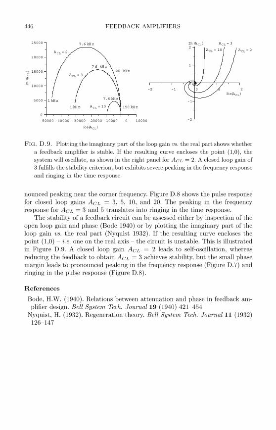
446 FEEDBACK AMPLIFIERS
-50000 -40000 -30000 -20000 -10000 0 10000
Re(ACL)
0
5000
10000
15000
20000
25000
Im(A
CL)
-2 -1 0 1 2Re(ACL)
-2
-1
0
1
2Im (ACL)
ACL = 2
ACL = 3
ACL = 10
ACL = 2
ACL = 3
ACL = 10
1 kHz
7.6 kHz
20 kHz
150 kHz
7.6 kHz
1 kHz
7.6 kHz
Fig. D.9. Plotting the imaginary part of the loop gain vs. the real part shows whether
a feedback amplifier is stable. If the resulting curve encloses the point (1,0), the
system will oscillate, as shown in the right panel for ACL = 2. A closed loop gain of
3 fulfills the stability criterion, but exhibits severe peaking in the frequency response
and ringing in the time response.
nounced peaking near the corner frequency. Figure D.8 shows the pulse responsefor closed loop gains ACL = 3, 5, 10, and 20. The peaking in the frequencyresponse for ACL = 3 and 5 translates into ringing in the time response.
The stability of a feedback circuit can be assessed either by inspection of theopen loop gain and phase (Bode 1940) or by plotting the imaginary part of theloop gain vs. the real part (Nyquist 1932). If the resulting curve encloses thepoint (1,0) – i.e. one on the real axis – the circuit is unstable. This is illustratedin Figure D.9. A closed loop gain ACL = 2 leads to self-oscillation, whereasreducing the feedback to obtain ACL = 3 achieves stability, but the small phasemargin leads to pronounced peaking in the frequency response (Figure D.7) andringing in the pulse response (Figure D.8).
References
Bode, H.W. (1940). Relations between attenuation and phase in feedback am-plifier design. Bell System Tech. Journal 19 (1940) 421–454
Nyquist, H. (1932). Regeneration theory. Bell System Tech. Journal 11 (1932)126–147
APPENDIX E
THE DIODE EQUATION
Before entering into a quantitative analysis of the diode characteristics, it isuseful to review the relationships that determine carrier concentrations. To avoidconfusion with exponential functions the symbol qe will be used for the electroniccharge instead of e. Furthermore, Ei denotes the intrinsic energy level, insteadof the ionization energy.
E.1 Carrier concentrations in pure semiconductors
In thermal equilibrium the probability that an electron state in the conductionband is filled is given by the Fermi–Dirac distribution
fe(E) =1
e(E−EF )/kT + 1. (E.1)
The parameter EF is the Fermi level (or chemical potential). Figure E.1 shows thedistribution for several temperatures. The density of atoms in a Si or Ge crystalis about 5 · 1022 atoms/cm3. Since the minimum carrier density of interest inpractical devices is of order 1010 to 1011 cm−3, very small occupancies are quiteimportant.
In silicon the bandgap is 1.12 eV. If the Fermi level is at midgap, the band-edges will be 0.56 eV above and below EF . As is apparent from Figure E.1,relatively large deviations from the Fermi level, i.e. extremely small occupancies,will still yield significant carrier densities.
0.6 0.8 1 1.2 1.4ENERGY IN UNITS OF THE FERM I LEVEL
0
0.2
0.4
0.6
0.8
1
OCCUPANCY
kT = 0.1
kT = 0.0.026 (300 K)
0.8 1 1.2 1.4 1.6 1.8ENERGY IN UNITS OF THE FERM I LEVEL
10-10
10-8
10-6
10-4
10-2
100
OCCUPANCY
kT = 0.026 eV (300 K)
kT = 0.035 eV (400 K)
kT = 0.005
Fig. E.1. The Fermi–Dirac distribution plotted for various temperatures.
447
448 THE DIODE EQUATION
0 1 2 3 4
ENERGY SPACING FROM EF IN UNITS OF kT
0.01
0.1
1
OCCUPANCY
BO LTZM ANNAPPROXIM ATION
FERM I−DIRACDISTRIBUTION
Fig. E.2. Comparison between the Fermi–Dirac and Boltzmann distributions.
The number of occupied electron states Ne is determined by summing overall available states multiplied by the occupation probability for each individualstate:
Ne =∑
i
mif(Ei) (E.2)
Since the density of states near the band edge tends to be quite high, this canbe written as an integral
Ne =
∞∫
Ec
f(E)g(E)dE , (E.3)
where g(E) is the density of states. Solution of this integral requires knowledgeof the density of states. Fortuitously, to a good approximation the density ofstates near the band edge has a parabolic distribution
g(E)dE ∝ (E − Ec)1/2 . (E.4)
As the energy increases beyond the band edge, the distribution will deviatefrom the simple parabolic form, but since the probability function decreasesvery rapidly, the integral will hardly be affected.
The second obstacle to a simple analytical solution of the integral is theintractability of integrating over the Fermi distribution. Fortunately, if E − EF
is at least several times kT , the Fermi distribution can be approximated by aBoltzmann distribution, as shown in Figure E.2.
1 + e(E−EF )/kT ≈ e(E−EF )/kT
CARRIER CONCENTRATIONS IN PURE SEMICONDUCTORS 449
f(E) ≈ e−(E−EF )/kT . (E.5)
At energies 2.3 kT beyond the Fermi level the difference between the Boltz-mann approximation and the Fermi distribution is < 10%, for energies > 4.5 kTit is less than 1%.
Applying the approximation to the occupancy of hole states, the probabilityof a hole state being occupied, i.e. a valence state being empty, is
fh(E) = 1 − fe(E) =1
e(EF −E)/kT + 1≈ e−(EF −E)/kT . (E.6)
The conditions for the Boltzmann approximation are fulfilled for excitation acrossthe bandgap, as the bandgap is of order 1 eV and kT at room temperature is0.026 eV.
With these simplifications the concentration of electrons in the conductionband in thermal equilibrium
n ∝ (kT )3/2e−(Ec−EF )/kT (E.7)
orn = Nce
−(Ec−EF )/kT , (E.8)
where Nc is the effective density of states at the band edge. Correspondingly,the hole concentration
p = Nve−(EF −Ev)/kT . (E.9)
In an ideal semiconductor the only source of mobile carriers is thermal excitationacross the bandgap (additional impurity atoms or crystal imperfections thatwould allow other excitation mechanisms are absent), so the concentrations ofelectrons and holes are equal,
n = p = ni . (E.10)
ni is called the intrinsic carrier concentration. In silicon (Eg = 1.12 eV) theintrinsic concentration ni = 1.45 · 1010 cm−3 at 300K and in germanium (Eg =0.66 eV), ni = 2.4·1013 cm−3. For comparison, the purest semiconductor materialthat has been fabricated is Ge with active impurity levels of about 3 ·1010 cm−3.
Using the above results
ni = Nce−(Ec−EF )/kT = Nve
−(EF −Ev)/kT , (E.11)
which one can solve to obtain
EF = Ei =Ec + Ev
2− kT
2log (Nc/Nv) . (E.12)
If the band structure is symmetrical (Nc = Nv), the intrinsic energy level Ei
lies near the middle of the bandgap. Even rather substantial deviations from
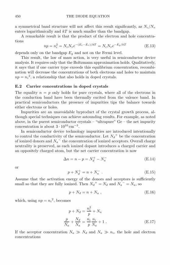
450 THE DIODE EQUATION
a symmetrical band structure will not affect this result significantly, as Nc/Nv
enters logarithmically and kT is much smaller than the bandgap.A remarkable result is that the product of the electron and hole concentra-
tionsnp = n2
i = NcNve−(Ec−Ev)/kT = NcNve
−Eg/kT (E.13)
depends only on the bandgap Eg and not on the Fermi level.This result, the law of mass action, is very useful in semiconductor device
analysis. It requires only that the Boltzmann approximation holds. Qualitatively,it says that if one carrier type exceeds this equilibrium concentration, recombi-nation will decrease the concentrations of both electrons and holes to maintainnp = ni
2, a relationship that also holds in doped crystals.
E.2 Carrier concentrations in doped crystals
The equality n = p only holds for pure crystals, where all of the electrons inthe conduction band have been thermally excited from the valence band. Inpractical semiconductors the presence of impurities tips the balance towardseither electrons or holes.
Impurities are an unavoidable byproduct of the crystal growth process, al-though special techniques can achieve astounding results. For example, as notedabove, in the purest semiconductor crystals – “ultrapure” Ge – the net impurityconcentration is about 3 · 1010 cm−3.
In semiconductor device technology impurities are introduced intentionallyto control the conductivity of the semiconductor. Let Nd
+ be the concentrationof ionized donors and Na
− the concentration of ionized acceptors. Overall chargeneutrality is preserved, as each ionized dopant introduces a charged carrier andan oppositely charged atom, but the net carrier concentration is now
∆n = n − p = N+d − N−
a (E.14)
orp + N+
d = n + N−a . (E.15)
Assume that the activation energy of the donors and acceptors is sufficientlysmall so that they are fully ionized. Then Nd
+ = Nd and Na− = Na, so
p + Nd = n + Na , (E.16)
which, using np = ni2, becomes
p + Nd =n2
i
p+ Na
p
Na+
Nd
Na=
ni
p
ni
Na+ 1 . (E.17)
If the acceptor concentration Na ≫ Nd and Na ≫ ni, the hole and electronconcentrations
pn-JUNCTIONS 451
p ≈ Na and n ≈ n2i
Na≪ Na , (E.18)
i.e. the conductivity is dominated by holes. Conversely, if the donor concentrationNd ≫ Na and Nd ≫ ni the conductivity is dominated by electrons.
If the conductivity is dominated by only one type of carrier, the Fermi levelis easy to determine. If, for example, n ≫ p then eqn E.16 can be written as
n = Nd − Na
Nce−(Ec−EF )/kT = Nd − Na , (E.19)
yieldingEc − EF
kBT= log
(
Nc
Nd − Na
)
. (E.20)
If Nd ≫ Na, then Ec − EF must be small, i.e. the Fermi level lies close to theconduction band edge.
In reality the impurity levels of common dopants are not close enough to theband edge for the Boltzmann approximation to hold, so the calculation must usethe Fermi distribution and solve numerically for EF . Nevertheless, the qualitativeconclusions derived here still apply.
It is often convenient to refer all of these quantities to the intrinsic level Ei,as it accounts for both Ec and Ev . Then
n = Nce−(Ec−EF )/kT = nie
−(EF−Ei)/kT
p = Nve−(EF −Ev)/kT = nie
−(Ei−EF )/kT (E.21)
and the Fermi level
EF − Ei = −kBT logNa − Nd
ni. (E.22)
E.3 pn-junctions
A pn-junction is formed at the interface of a p- and an n-type region. Since theelectron concentration in the n-region is greater than in the p-region, electronswill diffuse into the p-region. Correspondingly, holes will diffuse into the n-region.As electrons and holes diffuse across the junction, a space charge due to theionized donor and acceptor atoms builds up. The field due to this space chargeis directed to impede the flow of electrons and holes.
The situation is dynamic. The concentration gradient causes a continuousdiffusion current to flow, whereas the field due to the space charge drives a driftcurrent in the opposite direction. Equilibrium is attained when the two currentsare equal, i.e. the sum of the diffusion and drift currents is zero. The net holecurrent density is
Jp = −qeDpdp
dx+ qepµpEp , (E.23)
where Dp is the diffusion constant for holes and Ep is the electric field in thep-region.
452 THE DIODE EQUATION
To solve this equation we make use of the following relationships: The holeconcentration is
p = nie(Ei−EF )/kT , (E.24)
so its derivativedp
dx=
p
kT
(
dEi
dx− dEF
dx
)
. (E.25)
Since the force on a charge qe due to an electric field E is equal to the negativegradient of the potential energy,
qeE = −dEc
dx= −dEv
dx= −dEi
dx. (E.26)
As only the gradient is of interest and Ec, Ev , and Ei differ only by a constantoffset, any of these three measures can be used. We’ll use the intrinsic Fermilevel Ei, since it applies throughout the sample.
The remaining ingredient is the Einstein relationship, which relates the mo-bility to the diffusion constant
µp =qeDp
kT. (E.27)
Using these relationships the net hole current becomes
Jp = qepDp
kT
dEF
dx= µpp
dEF
dx. (E.28)
Accordingly, the net electron current
Jn = −qenDn
kT
dEF
dx= −µnn
dEF
dx. (E.29)
Since, individually, the net hole and electron currents in equilibrium must bezero, the derivative of the Fermi level
dEF
dx= 0 . (E.30)
In thermal equilibrium the Fermi level must be constant throughout the junctionregion.
For the Fermi level to be flat, the band structure must adapt, since on thep-side the Fermi level is near the valence band, whereas on the n-side it is nearthe conduction band (Figure 2.19). If we assume that the dopants are exclusivelydonors on the n-side and acceptors on the p-side, the difference in the respectiveFermi levels is
∆EF = −kT logNaNd
n2i
. (E.31)
This corresponds to an electric potential
∆VF =1
qe∆EF ≡ Vbi , (E.32)
often referred to as the “built-in” voltage of the junction.
THE FORWARD-BIASED pn-JUNCTION 453
As either Na or Nd increases relative to ni, the respective Fermi level movescloser to the band edge, increasing the built-in voltage. With increasing dopinglevels the built-in voltage approaches the equivalent potential of the bandgapEg/qe.
E.4 The forward-biased pn-junction
Applying an external bias leads to a condition that deviates from thermal equi-librium, i.e. the Fermi level is no longer constant throughout the junction. If apositive voltage is applied to the p-electrode relative to the n-electrode, the totalvariation of the electric potential across the junction will decrease (Figure 2.20).Since this reduces the electric field across the junction, the drift component ofthe junction current will decrease. Since the concentration gradient is unchanged,the diffusion current will exceed the drift current and a net current will flow.
This net current leads to an excess of electrons in the p-region and an excessof holes in the n-region. This “injection” condition leads to a local deviationfrom equilibrium, i.e. pn > ni
2. Equilibrium will be restored by recombination.Note that a depletion region exists even under forward bias, although its
width is decreased. The electric field due to the space charge opposes the flow ofcharge, but the large concentration gradient overrides the field.
Consider holes flowing into the n-region. They will flow through the deple-tion region with small losses due to recombination, as the electron concentrationis small compared with the bulk. When holes reach the n-side boundary of thedepletion region the concentration of electrons available for recombination in-creases and the concentration of holes will decrease with distance, depending onthe cross-section for recombination, expressed as a diffusion length. Ultimately,all holes will have recombined with electrons. The required electrons are fur-nished through the external contact from the power supply.
On the p-side, electrons undergo a similar process. The holes required tosustain recombination are formed at the external contact to the p-region byelectron flow toward the power supply, equal to the electron flow toward then-contact. The following derivation follows the discussions by Shockley (1949,1950) and Grove (1967).
The steady-state distribution of charge is determined by solving the diffusionequation,
Dnd2np
dx2− np − np0
τn= 0 . (E.33)
Electrons flowing into the p-region give rise to a local concentration np in excessof the equilibrium concentration np0. This excess will decay with a recombinationtime τn, corresponding to a diffusion length Ln.
The first boundary condition required for the solution of the diffusion equa-tion is that the excess concentration of electrons vanish at large distances x,
np(∞) = np0 . (E.34)
454 THE DIODE EQUATION
The second boundary condition is that the carriers are injected at the originof the space charge region x = 0 with a concentration np(0). This yields thesolution
np(x) = np0 + (np(0) − np0) e−x/Ln . (E.35)
From this we obtain the electron current entering the p-region
Jnp = −qeDndnp
dx
∣
∣
∣
∣
x=0
= qeDnnp(0) − np0
Ln. (E.36)
This says that the electron current is limited by the concentration gradient de-termined by the carrier density at the depletion edge np(0) and the equilibriumminority carrier density np0. Determining the equilibrium density np0 is easy,
np0 = n2i /Na . (E.37)
The problem is that np(0) is established in a non-equilibrium state, where thepreviously employed results do not apply.
To analyze the regions with non-equilibrium carrier concentrations Shockleyintroduced a simplifying assumption by postulating that the product pn is con-stant. In this specific quasi-equilibrium state this constant will be larger thanni
2, the pn-product in thermal equilibrium. In analogy to thermal equilibrium,this quasi-equilibrium state is expressed in terms of a “quasi-Fermi level”, whichis the quantity used in place of EF that gives the carrier concentration undernon-equilibrium conditions.
The postulate pn = const is equivalent to stating that the non-equilibriumcarrier concentrations are given by a Boltzmann distribution, so the concentra-tion of electrons is
n = nie(EF n−Ei)/kT , (E.38)
where EFn is the quasi-Fermi level for electrons, and
p = nie(Ei−EF p)/kT , (E.39)
where EFp is the quasi-Fermi level for holes. The product of the two carrierconcentrations in non-equilibrium is
pn = n2i e
(EF n−EF p)/kT . (E.40)
If pn is constant throughout the space-charge region, then EFn −EFp must alsoremain constant.
Using the quasi-Fermi level and the Einstein relationship, the electron currententering the p-region becomes
Jnp = −qeDndnp
dx
∣
∣
∣
∣
x=0
= −qeDnd
dx(nie
(EF n−Ei)/kBT ) = −µnndEFn
dx. (E.41)
These relationships describe the behavior of the quasi-Fermi level in the de-pletion region. How does this connect to the neutral region?
THE FORWARD-BIASED pn-JUNCTION 455
In the neutral regions the majority carrier motion is dominated by drift (incontrast to the injected minority carrier current, which is determined by diffu-sion). Consider the n-type region. Here the bulk electron current that providesthe junction current
Jnn = −µnndEi
dx. (E.42)
Since the two electron currents must be equal
Jnn = Jnp , (E.43)
it follows thatdEFn
dx=
dEi
dx, (E.44)
i.e. the quasi-Fermi level follows the energy band variation. Thus, in a neutralregion, the quasi-Fermi level for the majority carriers is the same as the Fermilevel in equilibrium. At current densities small enough not to cause significantvoltage drops in the neutral regions, the band diagram is flat, and hence thequasi-Fermi level is flat.
In the space charge region, pn is constant, so the quasi-Fermi levels for holesand electrons must be parallel, i.e. both will remain constant at their respectivemajority carrier equilibrium levels in the neutral regions.
If an external bias V is applied, the equilibrium Fermi levels are offset by V ,so it follows that the quasi-Fermi levels are also offset by V ,
EFn − EFp = qeV . (E.45)
Consequently, the pn-product in non-equilibrium
pn = n2i e
(EFn−EF p)/kT = n2i e
qeV/kT . (E.46)
If the majority carrier concentration is much greater than the concentrationdue to minority carrier injection (“low-level injection”), the hole concentrationat the edge of the p-region remains essentially at the equilibrium value. Conse-quently, the enhanced pn-product increases the electron concentration.
np(0) = np0eqeV/kT . (E.47)
Correspondingly, the hole concentration in the n-region at the edge of the deple-tion zone becomes
pn(0) = pn0eqeV/kT . (E.48)
Since the equilibrium concentrations
np0 =n2
i
Naand pn0 =
n2i
Nd, (E.49)
the components of the diffusion current due to holes and electrons are
Jn = qeDnn2
i
NaLn
(
eqeV/kT − 1)
456 THE DIODE EQUATION
Jp = qeDpn2
i
NdLp
(
eqeV/kT − 1)
. (E.50)
The total current is the sum of the electron and hole components
J = Jn + Jp = J0(eqeV/kT − 1) , (E.51)
where
J0 = qen2i
(
Dn
NaLn+
Dp
NdLp
)
. (E.52)
This is the diode equation (or Shockley equation), which describes the current–voltage characteristic both under forward and reverse bias. Under forward biasthe current increases exponentially. Under reverse bias (negative V ), the ex-ponential term vanishes when the bias exceeds several kT/qe and the currentbecomes the reverse saturation current J = −J0. For a uniform junction cross-section the current densities Jn, Jp, and J0 can be replaced by their respectivecurrents.
Note that in the diode equation:
1. The bandgap does not appear explicitly (only implicitly in J0 via ni).
2. The total current has two distinct components, due to electrons and holes.
3. The electron and hole currents are generally not equal. The ratio
Jn
Jp=
Nd
Naif
Dn
Ln=
Dp
Lp. (E.53)
4. Current flows for all values of V . However, when plotted on a linear scale,the exponential appears to have a knee, often referred to as the “turn-on”voltage.
5. The magnitude of the turn-on voltage is determined by J0. Diodes withdifferent bandgaps will show the same behavior if J0 is the same.
Figure E.3 shows measured I–V curves for commercial Si and Ge junctiondiodes (1N4148 and 1N34A). On a linear scale the Ge diode “turns on” at 200– 300mV, whereas the Si diode has a threshold of 500 – 600mV. However, ona logarithmic scale it becomes apparent that both diodes pass current at allvoltages > 0.
The reverse current (Figure E.4) shows why the Ge diode shows greatersensitivity at low voltages. The smaller bandgap leads to increased ni. The Sidiode shows a “textbook” exponential forward characteristic at currents > 10 nA,whereas the Ge diode exhibits a more complex structure.
The discrepancies in the forward current between the measured results andthe simple theory require the analysis of all processes in the depletion zone:
1. Generation-recombination in the depletion region (see Appendix F).
2. Diffusion current (as just calculated for the ideal diode).
THE FORWARD-BIASED pn-JUNCTION 457
0 200 400 600 800 1000
FORW ARD BIAS VOLTAGE (m V)
0
0.005
0.01
0.015
CURRENT(A) Si
G e
0 200 400 600 800 1000
FORW ARD BIAS VOLTAGE (m V)
10-10
10-8
10-6
10-4
10-2
CURRENT(A)
Si
Ge
Fig. E.3. Current vs. voltage for forward biased Si and Ge diodes.
3. High-injection region where the injected carrier concentration affects thepotentials in the neutral regions.
4. Voltage drop due to bulk series resistance.
For a discussion of these effects see Sze (1981).The reverse current is increased due to generation and recombination currents
in the depletion zone, as discussed in Appendix F. In optimized photodiodesreverse bias currents of about 100pA/cm2 have been achieved, which is about 3times the theoretical value (Holland 2004).
0 2 4 6 8 10
REVERSE BIAS VO LTAG E (V)
10-9
10-8
10-7
10-6
10-5
CURRENT(A)
Si
G e
Fig. E.4. Reverse current of Si and Ge diodes at room temperature.

458 THE DIODE EQUATION
References
Grove, A.S. (1967). Physics and Technology of Semiconductor Devices. Wiley,New York. ISBN 0-471-32998-3
Holland, S.E. (2004). private communicationShockley, W. (1949). The Theory of p−n junctions in Semiconductors and p−nJunction Transistors, Bell System Tech. Journal 28 (1949) 435–489
Shockley, W. (1950). Electrons and Holes in Semiconductors. van Nostrand,Princeton
Sze, S.M. (1981). Physics of Semiconductor Devices (2nd edn). Wiley, NewYork. ISBN 0-471-05661-8, TK7871.85.S988 1981
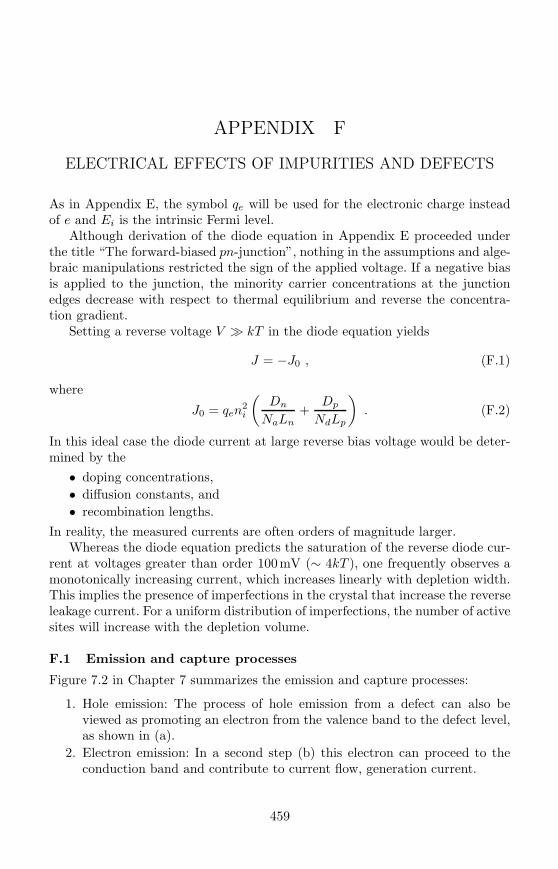
APPENDIX F
ELECTRICAL EFFECTS OF IMPURITIES AND DEFECTS
As in Appendix E, the symbol qe will be used for the electronic charge insteadof e and Ei is the intrinsic Fermi level.
Although derivation of the diode equation in Appendix E proceeded underthe title “The forward-biased pn-junction”, nothing in the assumptions and alge-braic manipulations restricted the sign of the applied voltage. If a negative biasis applied to the junction, the minority carrier concentrations at the junctionedges decrease with respect to thermal equilibrium and reverse the concentra-tion gradient.
Setting a reverse voltage V ≫ kT in the diode equation yields
J = −J0 , (F.1)
where
J0 = qen2i
(
Dn
NaLn+
Dp
NdLp
)
. (F.2)
In this ideal case the diode current at large reverse bias voltage would be deter-mined by the
• doping concentrations,
• diffusion constants, and
• recombination lengths.
In reality, the measured currents are often orders of magnitude larger.Whereas the diode equation predicts the saturation of the reverse diode cur-
rent at voltages greater than order 100mV (∼ 4kT ), one frequently observes amonotonically increasing current, which increases linearly with depletion width.This implies the presence of imperfections in the crystal that increase the reverseleakage current. For a uniform distribution of imperfections, the number of activesites will increase with the depletion volume.
F.1 Emission and capture processes
Figure 7.2 in Chapter 7 summarizes the emission and capture processes:
1. Hole emission: The process of hole emission from a defect can also beviewed as promoting an electron from the valence band to the defect level,as shown in (a).
2. Electron emission: In a second step (b) this electron can proceed to theconduction band and contribute to current flow, generation current.
459
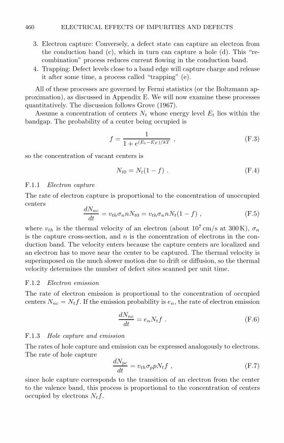
460 ELECTRICAL EFFECTS OF IMPURITIES AND DEFECTS
3. Electron capture: Conversely, a defect state can capture an electron fromthe conduction band (c), which in turn can capture a hole (d). This “re-combination” process reduces current flowing in the conduction band.
4. Trapping: Defect levels close to a band edge will capture charge and releaseit after some time, a process called “trapping” (e).
All of these processes are governed by Fermi statistics (or the Boltzmann ap-proximation), as discussed in Appendix E. We will now examine these processesquantitatively. The discussion follows Grove (1967).
Assume a concentration of centers Nt whose energy level Et lies within thebandgap. The probability of a center being occupied is
f =1
1 + e(Et−EF )/kT, (F.3)
so the concentration of vacant centers is
Nt0 = Nt(1 − f) . (F.4)
F.1.1 Electron capture
The rate of electron capture is proportional to the concentration of unoccupiedcenters
dNnc
dt= vthσnnNt0 = vthσnnNt(1 − f) , (F.5)
where vth is the thermal velocity of an electron (about 107 cm/s at 300K), σn
is the capture cross-section, and n is the concentration of electrons in the con-duction band. The velocity enters because the capture centers are localized andan electron has to move near the center to be captured. The thermal velocity issuperimposed on the much slower motion due to drift or diffusion, so the thermalvelocity determines the number of defect sites scanned per unit time.
F.1.2 Electron emission
The rate of electron emission is proportional to the concentration of occupiedcenters Nnc = Ntf . If the emission probability is en, the rate of electron emission
dNne
dt= enNtf . (F.6)
F.1.3 Hole capture and emission
The rates of hole capture and emission can be expressed analogously to electrons.The rate of hole capture
dNpc
dt= vthσppNtf , (F.7)
since hole capture corresponds to the transition of an electron from the centerto the valence band, this process is proportional to the concentration of centersoccupied by electrons Ntf .
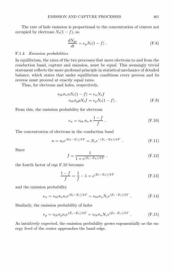
EMISSION AND CAPTURE PROCESSES 461
The rate of hole emission is proportional to the concentration of centers notoccupied by electrons Nt(1 − f), so
dNpe
dt= epNt(1 − f) . (F.8)
F.1.4 Emission probabilities
In equilibrium, the rates of the two processes that move electrons to and from theconduction band, capture and emission, must be equal. This seemingly trivialstatement reflects the more profound principle in statistical mechanics of detailedbalance, which states that under equilibrium conditions every process and itsreverse must proceed at exactly equal rates.
Thus, for electrons and holes, respectively,
vthσnnNt(1 − f) = enNtf
vthσppNtf = epNt(1 − f) . (F.9)
From this, the emission probability for electrons
en = vth σn n1 − f
f. (F.10)
The concentration of electrons in the conduction band
n = nie(EF −Ei)/kT = Nce
−(Ec−EF )/kT . (F.11)
Since
f =1
1 + e(Et−EF )/kT, (F.12)
the fourth factor of eqn F.10 becomes
1 − f
f=
1
f− 1 = e(Et−EF )/kT (F.13)
and the emission probability
en = vthσnnie(Et−Ei)/kT = vthσnNce
(Ec−Ei)/kT . (F.14)
Similarly, the emission probability of holes
ep = vthσpnie(Ei−Et)/kT = vthσnNve(Et−Ev)/kT . (F.15)
As intuitively expected, the emission probability grows exponentially as the en-ergy level of the center approaches the band edge.
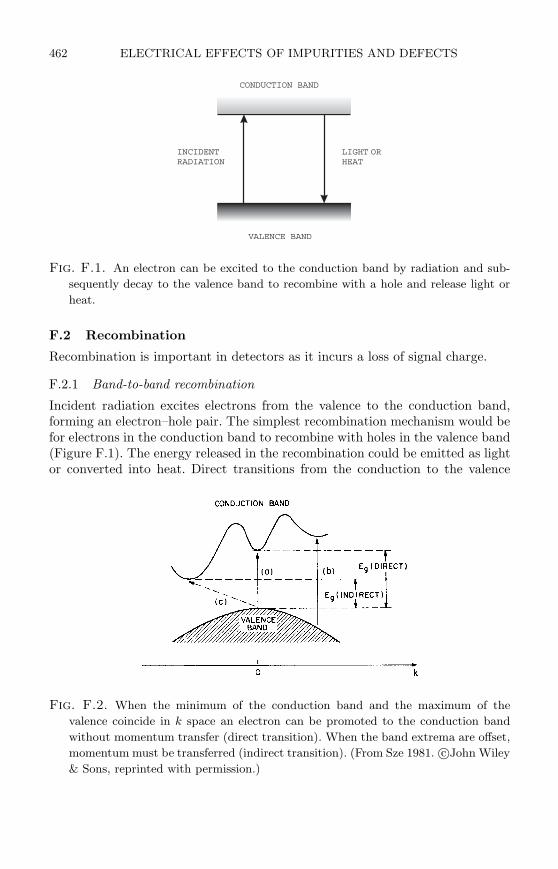
462 ELECTRICAL EFFECTS OF IMPURITIES AND DEFECTS
CONDUCTION BAND
VALENCE BAND
INCIDENTRADIATION
LIGHT ORHEAT
Fig. F.1. An electron can be excited to the conduction band by radiation and sub-
sequently decay to the valence band to recombine with a hole and release light or
heat.
F.2 Recombination
Recombination is important in detectors as it incurs a loss of signal charge.
F.2.1 Band-to-band recombination
Incident radiation excites electrons from the valence to the conduction band,forming an electron–hole pair. The simplest recombination mechanism would befor electrons in the conduction band to recombine with holes in the valence band(Figure F.1). The energy released in the recombination could be emitted as lightor converted into heat. Direct transitions from the conduction to the valence
Fig. F.2. When the minimum of the conduction band and the maximum of the
valence coincide in k space an electron can be promoted to the conduction band
without momentum transfer (direct transition). When the band extrema are offset,
momentum must be transferred (indirect transition). (From Sze 1981. c©John Wiley
& Sons, reprinted with permission.)
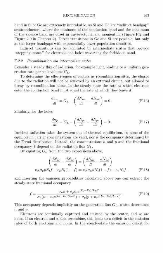
RECOMBINATION 463
band in Si or Ge are extremely improbable, as Si and Ge are “indirect bandgap”semiconductors, where the minimum of the conduction band and the maximumof the valence band are offset in wavevector k, i.e. momentum (Figure F.2 andFigure 2.9 in Chapter 2). Direct transitions in Ge and Si are possible, but onlyat the larger bandgaps with exponentially lower population densities.
Indirect transitions can be facilitated by intermediate states that provide“stepping stones” for electrons and holes traversing the forbidden band.
F.2.2 Recombination via intermediate states
Consider a steady flux of radiation, for example light, leading to a uniform gen-eration rate per unit volume GL.
To determine the effectiveness of centers as recombination sites, the chargedue to the radiation will not be removed by an external circuit, but allowed todecay by recombination alone. In the steady state the rate at which electronsenter the conduction band must equal the rate at which they leave it:
dnn
dt= GL −
(
dNnc
dt− dNne
dt
)
= 0 . (F.16)
Similarly, for the holes
dnp
dt= GL −
(
dNpc
dt− dNpe
dt
)
= 0 . (F.17)
Incident radiation takes the system out of thermal equilibrium, so none of theequilibrium carrier concentrations are valid, nor is the occupancy determined bythe Fermi distribution. Instead, the concentrations n and p and the fractionaloccupancy f depend on the radiation flux GL.
By equating GL from the two expressions above,
(
dNpc
dt− dNpe
dt
)
=
(
dNnc
dt− dNne
dt
)
vthσppNtf − epNt(1 − f) = vthσnnNt(1 − f) − enNtf , (F.18)
and inserting the emission probabilities calculated above one can extract thesteady state fractional occupancy
f =σnn + σpnie
(Ei−Et)/kBT
σn(n + nie(Et−Ei)/kBT ) + σp(p + nie(Ei−Et)/kBT ). (F.19)
This occupancy depends implicitly on the generation flux GL, which determinesn and p.
Electrons are continually captured and emitted by the center, and so areholes. If an electron and a hole recombine, this leads to a deficit in the emissionrates of both electrons and holes. In the steady-state the emission deficit for
464 ELECTRICAL EFFECTS OF IMPURITIES AND DEFECTS
electrons and holes must be equal, so the net rate of recombination is the capturerate minus the emission rate
dNR
dt=
(
dNnc
dt− dNne
dt
)
=
(
dNpc
dt− dNpe
dt
)
. (F.20)
This is the same expression as above, so one can determine the recombinationrate by inserting the steady state fractional occupancy into either side of eqnF.18,
dNR
dt=
σpσnvthNt(pn − n2i )
σn(n + nie(Et−Ei)/kBT ) + σp(p + nie(Ei−Et)/kBT ). (F.21)
To simplify the equation and facilitate the interpretation of this result, assume(somewhat arbitrarily) that the capture cross-sections σn and σp are equal. Then
dNR
dt= σvthNt
pn − n2i
n + p + 2ni(e(Et−Ei)/kBT + e−(Et−Ei)/kBT ). (F.22)
From this expression one can see that the driving force of the recombination pro-cess is the excess carrier concentration pn beyond the equilibrium concentrationni
2.The third term in the denominator describes the relative occupancies of elec-
trons and holes. A center close to the conduction band will have a higher occu-pancy of electrons than holes, so the recombination rate is limited by the holepopulation. Conversely, a center close to the valence band will have an excess ofholes, so the population of electrons limits the recombination rate. The recombi-nation rate is maximum when Et = Ei, i.e. when the energy of the recombinationcenter is at mid-gap.
A special case of recombination is minority carrier injection. Consider holesinjected into an n-type region, as in a forward biased diode. In this case
nn ≫ pn . (F.23)
Furthermore, since efficient recombination centers are far from the band edge,the Boltzmann approximation holds, so the equilibrium electron concentration
nn ≫ nie(Et−Ei)/kBT . (F.24)
Then the above expression for the recombination rate simplifies to
dNR
dt=
σpσnvthNt(nnpn − n2i )
σnnn= σpvthNt(pn − pn0) . (F.25)
Expressed as a lifetimedNR
dt=
p − pn0
τp, (F.26)
CARRIER GENERATION 465
so the carrier lifetime
τp =1
σpvthNt. (F.27)
The lifetime of the holes in the n-bulk is independent of the concentration of theelectrons.
This is due to an abundance of electrons, so as soon as a hole is captured, anelectron is available for immediate recombination. Hence, the hole concentrationis the rate-limiting parameter. Conversely, if electrons are injected into n-typematerial where they are majority carriers, their lifetime will be significantlygreater, since few holes are available for recombination.
Minority carrier injection is the worst case with respect to recombination, so“minority carrier lifetime” is a figure of merit used to characterize the presenceof defects in semiconductors.
Recombination is important whenever the carrier concentration deviates fromthermal equilibrium
pn > n2i . (F.28)
This occurs
• with incident radiation,
• in a forward biased diode.
F.3 Carrier generation
F.3.1 Generation in the depletion region
In a diode operated with reverse bias, e.g. a radiation detector, with
VR ≫ kT
qe(F.29)
all of the free carriers are swept from the depletion region, so there are no freecarriers available for capture and recombination. In this configuration only emis-sion processes are important.
Emission, in the absence of capture, can only proceed by alternating hole andelectron emission, i.e. generation of electron–hole pairs. The rate of generationof electron–hole pairs can be determined from the previously derived expressionseqns F.20 and F.21 for the difference between capture and emission rates
dNc
dt− dNe
dt=
σpσnvthNt(pn − n2i )
σn(n + nie(Et−Ei)/kBT ) + σp(p + nie(Ei−Et)/kBT ). (F.30)
Since dNc/dt = 0 and p ≪ ni , n ≪ ni,
dNe
dt=
σpσnvthNtni
σne(Et−Ei)/kBT + σpe(Ei−Et)/kBT. (F.31)
This is often written asdNe
dt≡ ni
2τg, (F.32)
where τg is called the generation lifetime.
466 ELECTRICAL EFFECTS OF IMPURITIES AND DEFECTS
Again consider the simplified case of equal cross-sections σp = σn = σ. Thenthe generation rate becomes
dNe
dt=
σvthNtni
e(Ei−Et)/kBT + e−(Ei−Et)/kBT, (F.33)
which again shows that only states near the intrinsic Fermi level Ei, i.e. mid-gapstates, contribute significantly to the generation rate.
Intuitively, this is easy to see in the “stepping stone” picture. Since the emis-sion probabilities for electrons and holes increase exponentially with the sepa-ration from their respective band edges, the probability for sequential hole andelectron emission is maximum at mid-gap.
The emission rate of carriers leads to an electrical current, the generationcurrent, which increases with the density of centers. If the emission centers aredistributed uniformly throughout the depletion width W , the generation currentdensity
Jgen = qedNe
dtW = qeW
σvthNtni
e(Ei−Et)/kBT + e−(Ei−Et)/kBT. (F.34)
F.3.2 Generation in the neutral region
In the neutral region the absence of a significant electric field means that anyexcess carriers due to generation move only by diffusion. Charges generated nearthe transition to the depletion region can reach the influence of the electric fieldand will be swept to the opposite electrode. This additional contribution to thereverse diode current is called the diffusion current.
The starting point of the calculation is the steady-state diffusion equationfor minority carriers. Consider electrons generated in the p-region:
Dnd2np
dx2− np − np0
τn= 0 . (F.35)
Far from the space charge region the carrier concentration attains the thermalequilibrium value
np(∞) = np0 . (F.36)
At the edge of the depletion region all carriers will be swept away by the electricfield, so
np(0) = 0 . (F.37)
The solution of the diffusion equation for these boundary conditions is
np(x) = np0(1 − e−x/Ln) , (F.38)
whereLn ≡
√
Dnτn (F.39)
is the diffusion length of electrons in the p-region.
THE ORIGIN OF RECOMBINATION AND GENERATION CENTERS 467
This gives rise to an electrical current
Jdiff,n = −qe
(
−Dndnp
dx
∣
∣
∣
∣
x=0
)
= qeDnnp0
Ln= qe
Dn
Ln
n2i
Na. (F.40)
Similarly, for holes in the n-region
Jdiff,p = qeDppn0
Lp= qe
Dp
Lp
n2i
Nd. (F.41)
The diffusion current increases with the square of the intrinsic carrier concentra-tion, in contrast to the generation current in the depletion zone, which increaseslinearly with ni.
The generation rate in a neutral region depleted of minority carriers can bedrastically different from the depletion region. For simplicity, assume that thediffusion lifetime is equal to the generation lifetime. Then the ratio of the twogeneration currents
Jdiff,n
Jgen=
np0
τLn
ni
2τW
= 2np0
ni
Ln
W= 2
ni
Na
Ln
W. (F.42)
In an n-bulk Si radiation detector with a thin p-electrode, the diffusion lengthis limited by the electrode thickness, i.e. ∼ 1 µm. For ni ≈ 1010 cm−3, Na ≈1015 cm−3, and W ≈ 300 µm
Jdiff,n
Jgen≈ 3 · 10−8 .
In high-quality radiation detectors the generation current dominates.By contrast, in a symmetrical Ge small signal rectifier diode with Ln ≈
100 µm, W ≈ 1 µm, ni ≈ 1013 cm−3, and Na ≈ 1015 cm−3,
Jdiff,n
Jgen≈ 2 .
At higher temperatures the exponential increase in ni can increase the diffusioncurrent so much that the generation current is negligible.
F.4 The origin of recombination and generation centers
Recombination and generation centers can be introduced by
1. impurity atoms,
2. structural imperfections,
3. radiation damage (displacement of atoms from lattice sites).
468 ELECTRICAL EFFECTS OF IMPURITIES AND DEFECTS
Figure F.3 shows the energy levels of impurities in Si and GaAs crystals. Mn, Cd,Zn, Au, Co, V and Fe are effective “lifetime killers” in Si. Au is commonly intro-duced intentionally in devices where short lifetimes are desirable (fast switchingdiodes and transistors).
All three defect mechanisms can create states distributed throughout thebandgap Since only mid-gap states can contribute significantly to generation andrecombination, in a continuum of states statistics automatically select the statesnear mid-gap. Indirect bandgap materials show reduced transition probabilities,as the mismatch in k-space must be bridged.
GaAs appears favorable, since relatively few impurity states are near mid-gap.However, a structural defect tends to dominate: The “anti-site” defect, where aGa atom occupies an As site (or vice versa) and introduces a mid-gap statethat effectively pins the Fermi level at mid-gap. This is why GaAs commonlyappears intrinsic, or “semi-insulating”, so that large depletion widths can beobtained with small reverse bias voltages. Unfortunately, recombination is alsohigh, although for some applications acceptable in thin (∼ 102µm) detectors.
F.5 The diode equation revisited
F.5.1 Reverse Current
Both the generation and diffusion currents invariably override the ideal reversesaturation current
J0 = qen2i
(
Dn
NaLn+
Dp
NdLp
)
<< Jdiff + Jgen , (F.43)
so the diode equation becomes
J = JR(eqeV/kT − 1) . (F.44)
The reverse current JR for voltages > 3kT/qe is the sum of the diffusion andgeneration currents
JR = qen2i
(
1
Na
√
Dn
τn+
1
Nd
√
Dp
τp
)
+ qeni
2τgW . (F.45)
Whether the generation or diffusion current dominates can be determined fromthe temperature coefficient. The diffusion current scales with ni
2, so
dJR
dT= JR
Eg
kT 2, (F.46)
whereas the generation current scales with ni, yielding
dJR
dT= JR
Eg
2kT 2. (F.47)
In practice, a plot of log JR vs. 1/kT will yield a slope of −Eg for diffusion andapproximately −Eg/2 for generation dominated operation. At sufficiently hightemperatures diffusion will always dominate.
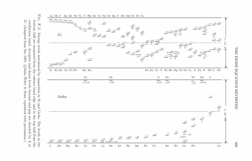
TH
ED
IOD
EE
QU
AT
ION
RE
VIS
ITE
D469
1.12
eV
1.42
eV
Si
GaAs
.63A
.4
.0059.03
Si Ge
C Be Mg Zn Ag Pb Co NiSn Cu Fe CrSi Cd Li Ge Au Mn
S Sn Te Se O
.045.067.072
.16
.3.34
.033.039.045.054.069.14
.21.25
.25.25
.11
A
.40.41
.14
.43
.30.32.26
.43.36A
.20A
.45A
.25A .34
A
.55A
.54A
.53.49
.35.33.31
A
A
.28 .27 .26.25.22
.30
.37
.17.16.14
.38A.51 .51
Li Sb P As Bi Te Ti C Mg Se Cr Ta Cs Ba S Mn Ag Cd Pt Si
B Al Ga In Tl Pd Na Be Zn Au Co V Ni Mo Hg Sr Ge Cu K Sn W Pb O Fe
.35D
.42
.17
.50.50.48.45
.53
.33
.55
.30.36
.49
.19D
D
.26.29D
A.49
.35.40
.23.30D
.34D .33
.25D
D
.50D
.50D
.24
.40
.53
.35D .27
.34
.31D
D.37
.41.40
D
.36
D.30
.026 .028 .028 .031 .035 .035 .05.023
.07
.04
.09 .095 .11 .12.16 .17
.21
.14
.023
.24
.44
.19
.37
.52D
.53D
.67
.006.006.006.0058
Fig
.F.3
.E
nerg
ylev
elsin
troduced
by
impurities
inSiand
GaA
s.T
he
levels
inth
e
botto
mhalf
are
mea
sured
from
the
valen
ceband
edge
and
inth
eto
phalf
from
the
conductio
nband.A
ccepto
rand
donor
levels
bey
ond
mid
-gap
are
den
oted
by
Aor
D.(A
dapted
from
Sze
1981.
c©John
Wiley
&Sons,
reprin
tedw
ithperm
ission.)
470 ELECTRICAL EFFECTS OF IMPURITIES AND DEFECTS
In radiation damaged diodes the generation current dominates even afterrather low fluences, so the reverse bias current
IR(T ) ∝ vthni ∝ vth
√
NcNve−E/2kT ∝ T 2e−E/2kT , (F.48)
where E ≈ Eg , depending on the impurity or defect energy level. The ratio ofcurrents at two temperatures T1 and T2 is
IR(T2)
IR(T1)=
(
T2
T1
)2
exp
[
− E
2k
(
T1 − T2
T1T2
)]
. (F.49)
Cooling to 0 C typically reduces the reverse bias current to 1/6 of its valueat room temperature. As discussed in Chapter 7, after irradiation the leakagecurrent initially decreases with time. Pronounced short term and long term an-nealing components are observed and precise fits to the annealing curve requirea sum of exponentials.
In practice, the variation of leakage current with temperature is very re-producible from device to device, even after substantial doping changes due toradiation damage. The leakage current can be used for dosimetry and diodes areoffered commercially specifically for this purpose.
F.5.2 Forward current
Recombination in the depletion region also affects the forward diode characteris-tic. Experimental results can generally be described by introducing an “idealityfactor” n
J = JR(eqeV/nkT − 1) , (F.50)
where n = 2 when the recombination current dominates and n = 1 when thecurrent is dominated by diffusion in the neutral regions. In practical diodes nlies between 1 and 2.
At very low currents the generation currents dominate. Since these currentsare opposite to the forward injection current, one observes a change of sign inthe current flow at low voltage.
F.5.3 Comments
In radiation detectors the reverse current is of primary interest, as it is a sourceof shot noise. Nevertheless, the forward current–voltage characteristic can pro-vide useful diagnostic information. Since recombination and generation are bothmaximized for mid-gap states, one commonly observes that devices with largegeneration currents also exhibit high recombination rates.
This has promoted a tendency to characterize both phenomena by one pa-rameter, the minority carrier lifetime. However, generation and recombinationare two distinct phenomena. First, their temperature dependencies differ, andsecond, it is not at all assured that a state is equally effective at generation as itis at recombination.
REFERENCES 471
References
Grove, A.S. (1967). Physics and Technology of Semiconductor Devices. Wiley,New York. ISBN 0-471-32998-3
Sze, S.M. (1981). Physics of Semiconductor Devices (2nd edn). Wiley, NewYork. ISBN 0-471-05661-8, TK7871.85.S988 1981
APPENDIX G
BIPOLAR TRANSISTOR EQUATIONS
The basic processes in an npn bipolar junction transistor are summarized below.
1. Holes are injected into the base through the external contact. The poten-tial distribution drives them towards the emitter. Since they are majoritycarriers in the base, few will recombine. Holes entering the base–emitterdepletion region will either
(a) pass through the depletion region into the emitter or
(b) be lost due to recombination.
2. As shown in the discussion of the pn-junction (Appendix E), coupled withthe hole current is an electron current originating in the emitter. Thiselectron current will flow towards the collector, driven by the more positivepotential. These electrons either
(a) enter the collector to become the collector current or(b) recombine in the base region. The holes required for the recombination
are furnished by the base current.
3. Thus, the base current is the sum of the
(a) hole current entering the emitter,
(b) hole losses due to recombination in the base–emitter depletion region,and
(c) electron losses due to recombination in the base during transport tothe collector.
The goal is to maximize 2(a) and 3(a).As in Appendix E, the discussion follows Grove (1967) and the symbol qe will
be used for the electronic charge instead of e to avoid confusion with exponentialfunctions.
The transport of minority carriers in the base is driven by diffusion, so
Dnd2np
dx2− np − np0
τn= 0 . (G.1)
At the boundary to the base–emitter depletion region
np(0) = np0eqeVBEe/kT . (G.2)
The equilibrium concentration of electrons in the base is determined by the baseacceptor doping level NaB
np0 =n2
i
NaB. (G.3)
472
BIPOLAR TRANSISTOR EQUATIONS 473
At the collector boundary all minority carriers will be immediately swept awayby the reverse bias field, so that the boundary condition becomes
np(WB) = 0 . (G.4)
Then the solution of the diffusion equation is
np(x) = np0
1 −sinh
x
Ln
sinhWB
Ln
+ (np(0) − np0)sinh
WB − x
Ln
sinhWB
Ln
. (G.5)
If VBE ≫ 4kT/qe the non-equilibrium concentration will dominate,
np(0) ≫ np0 , (G.6)
so this simplifies to
np(x) = np(0)sinh
WB − x
Ln
sinhWB
Ln
. (G.7)
Since the base width WB in good transistors is much smaller than the diffusionlength Ln, the concentration profile can be approximated by a linear distribution
np(x) = np(0)
(
1 − x
WB
)
. (G.8)
Now we can evaluate the individual current components. In this approximationthe diffusion current of electrons in the base region becomes
JnB = −qeDnBdnp(x)
dx= qeDnB
n2i
NaBWBeqeVBE/kT , (G.9)
where DnB is the diffusion constant of electrons in the base. Similarly, the dif-fusion current of holes injected into the emitter, under the assumption that theemitter depth WE is much smaller than the diffusion length,
JpE = qeDpEn2
i
NdEWEeqeVBE/kT . (G.10)
For the moment, we’ll neglect recombination of holes in the base–emitter deple-tion region. Under this assumption, the base current is
IB = JpEAJE , (G.11)
where AJE is the area of the emitter junction.
474 BIPOLAR TRANSISTOR EQUATIONS
The collector current is primarily the electron current injected into the base,minus any losses due to recombination during diffusion. The collector transportfactor
αT =electron current reaching collector
electron current injected from emitter=
dnp
dx
∣
∣
∣
∣
x=WB
dnp
dx
∣
∣
∣
∣
x=0
. (G.12)
Using the above result this becomes
αT =1
coshWB
Ln
. (G.13)
Recalling that the base width is to be much smaller than the diffusion length,this expression can be approximated as
αT ≈ 1 − 1
2
(
WB
Ln
)2
. (G.14)
In modern devices α ≈ 1. The resulting collector current is the diffusion currentof electrons in the base times the transport factor
IC = JnBAJEαT . (G.15)
One of the most interesting parameters of a bipolar transistor is the directcurrent gain (DC gain), which is the ratio of collector current to base current
βDC =IC
IB. (G.16)
Using the above results
βDC =qeDnB
n2i
NaBWBeqeVBE/kT
qeDpEn2
i
NdEWEeqeVBE/kT
βDC =NdE
NaB· DnBWE
DpEWB. (G.17)
Primarily, the DC gain is determined by the ratio of doping concentrations inthe emitter and the base. This simple result reflects the distribution of currentin the forward biased diode between electrons and holes. Transistors with highcurrent gains always have much higher doping levels in the emitter than in thebase.
BIPOLAR TRANSISTOR EQUATIONS 475
The result of this idealized analysis implies that for a given device the DCgain should be independent of current. In reality this is not the case. Althoughmodern transistors show a roughly constant current gain over decades of current,the current gain falls off both at very low and at high currents.
The decrease at low currents is due to recombination in the base–emitterdepletion region. Since the most efficient recombination centers are near themiddle of the bandgap, we set Et = Ei to obtain the recombination rate
dNR
dt= σvthNt
pn − n2i
n + p + 2ni. (G.18)
Due to quasi-equilibrium in the space charge region
pn = n2i e
qeVBE/kT . (G.19)
This gives us the product of electron concentrations, but we also need the indi-vidual concentrations.
For a given forward bias the maximum recombination rate will coincide withthe minimum concentration, i.e.
d(p + n) = 0 (G.20)
and since pn = const,
dp = −dn =pn
p2dp (G.21)
orp = n (G.22)
at the point of maximum recombination. Hence, the carrier concentrations are
pn = n2 = p2 = n2i e
qeVBE/kT (G.23)
orn = p = nie
qeVBE/2kT . (G.24)
Inserting these concentrations into the expression for the recombination rate eqnG.18 yields
dNR
dt= σvthNt
n2i (e
qeVBE/kT − 1)
2ni(eqeVBE/2kT + 1). (G.25)
This maximum recombination rate will not prevail throughout the depletionregion, but only over a region where the potential changes no more than ∼ kT/qe.
476 BIPOLAR TRANSISTOR EQUATIONS
If we assume that the average field is VBE/WBE , a suitable averaging distanceis
w =kT
qe
WBE
VBE. (G.26)
Nevertheless, for simplicity assume that recombination is uniform throughoutthe depletion region. For VBE ≫ kT/qe this yields the recombination current tobe made up by holes from the base current
Jpr = qedNR
dt≈ 1
2qeσvthNtniWBEeqeVBE/2kT . (G.27)
Now the base current becomes
IB = (JpE + JR)AJE , (G.28)
so the DC gain with recombination is
βDC =qeDnB
n2i
NaBWBeqeVBE/kT
qeDpEn2
i
NdEWEeqeVBE/kT +
1
2qeσvthNtniWeqeVBE/2kBT
. (G.29)
Because of the factor 1/2 in the exponent of the recombination term
βDC =DnB
n2i
NaBWB
DpEn2
i
NdEWE+
ni
2τ0WBEe−qeVBE/2kT
, (G.30)
which can be rewritten in a more informative form as
1
βDC=
1
β0+
NaBWBE
DnBWB
Ntσvth
nieqeVBE/2kT, (G.31)
where β0 is the DC gain without recombination. Increasing the concentration oftraps Nt decreases the current gain βDC , whereas decreasing the base width WB
reduces the effect of traps. Since a smaller base width translates to increasedspeed (reduced transit time through the base), fast transistors tend to be lesssensitive to trapping.
The current dependence enters through the exponential, which relates theinjected carrier concentrations to the base–emitter voltage VBE . With decreasingvalues of base–emitter voltage, i.e. decreasing current, recombination becomesmore important. This means that the DC gain is essentially independent ofcurrent above some current level, but will decrease at lower currents.
Furthermore note that – although not explicit in the above expression – the“ideal” DC gain depends only on device and material constants, whereas therecombination depends on the local density of injected electrons and holes with
REFERENCES 477
respect to the concentration of recombination centers. Consider two transistorswith different emitter areas, but operating at the same current, so the largertransistor operates at a lower current density. The larger area transistor willachieve a given current at a lower base–emitter voltage VBE than the smallerdevice, which increases the effect of trapping. Thus, the relative degradation ofDC gain due to recombination depends on the current density.
This means that within a given fabrication process, a large transistor willexhibit more recombination than a small transistor at the same current. Stateddifferently, for a given current, the large transistor will offer more recombinationcenters for the same number of carriers.
Measured current gains vs. current are shown in Chapter 6. Data in Chapter7 show the degradation of current gain after irradiation. Radiation damage in-creases the concentration of trapping sites Nt proportional to fluence Φ, so theabove equation can be rewritten to express the degradation of current gain withfluence for a given current density (fixed VBE):
1
βDC=
1
β0+ KΦ , (G.32)
where the constant K encompasses the device constants and operating point.In a radiation-damaged transistor the reduction in current gain for a given DCcurrent will be less for smaller devices and furthermore faster transistors (smallbase width) will be less sensitive to radiation damage.
Why does the DC gain drop off at high currents?
1. With increasing current the high field region shifts towards the collector,effectively increasing the base width (“Kirk effect”).
2. At high current levels the injected carrier concentration becomes compara-ble with the bulk doping. This reduces the injection efficiency and at veryhigh current densities leads to bandgap narrowing.
3. Voltage drops in base and emitter resistance reduce the effective base–emitter and collector voltages.
4. Auger recombination.
For a discussion of these effects see Sze (1981).
References
Grove, A.S. (1967). Physics and Technology of Semiconductor Devices. Wiley,New York. ISBN 0-471-32998-3
Sze, S.M. (1981). Physics of Semiconductor Devices (2nd edn). Wiley, NewYork. ISBN 0-471-05661-8, TK7871.85.S988 1981