semiconductor detector development and processing laboratory
TRANSCRIPT
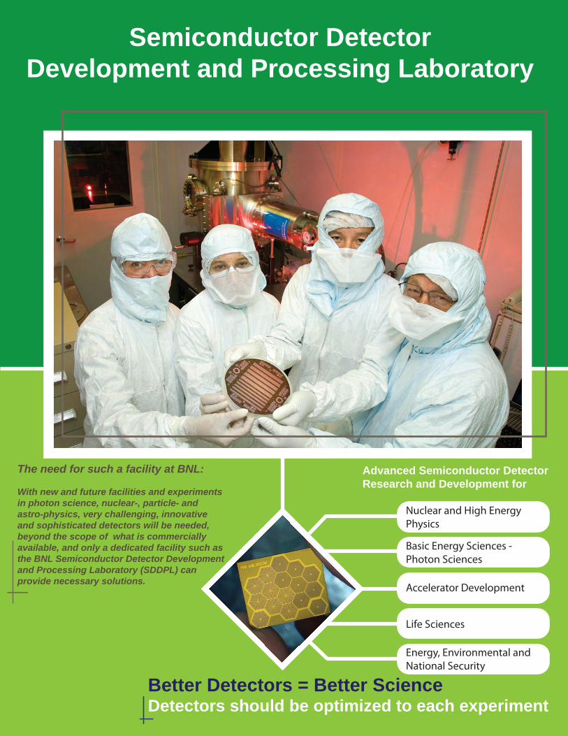
Semiconductor DetectorDevelopment and Processing Laboratory
Semiconductor Detector Development and Processing LaboratoryInstrumentation Division
Brookhaven National LaboratoryUpton, NY 11973
Advanced Semiconductor DetectorResearch and Development for
Nuclear and High EnergyPhysics
Basic Energy Sciences -Photon Sciences
Life Sciences
Energy, Environmental andNational Security
Accelerator Development
10-20-2008/AK
Better Detectors = Better ScienceDetectors should be optimized to each experiment
The need for such a facility at BNL:
With new and future facilities and experiments in photon science, nuclear-, particle- and astro-physics, very challenging, innovative and sophisticated detectors will be needed, beyond the scope of what is commercially available, and only a dedicated facility such as the BNL Semiconductor Detector Development and Processing Laboratory (SDDPL) can provide necessary solutions.

Brookhaven National Laboratory’s Semiconductor Detector Developmentand Processing Lab (SDDPL) is a unique facility that has been developing detectors for more than 20 years, serving the scientific community in the United States and abroad. Detectors developed and fabricated in the Instrumentation Division have been used in nuclear and high energy physics, photon (material and life) science and experiments for X-ray astronomy.
The 500 sq ft Class-100 cleanroom supports detector and monolithic JFET technology in 4” and 6” high resistivity ( ≥ 4000 Ω-cm) silicon (Si) wafers.
SDDPL is staffed by 1 Ph.D. and 1 Professional from Instrumentation, 1 Ph.D. from NSLS and 1 Professional from Physics.
Simulation and DesignDedicated software for 2-D and 3-D simulation of semiconductor processing and devices is used for implementing new concepts in fabrication and design. The close collaboration of physicists and engineers is vital for making new ideas a reality for specific experiment needs. A good simulation will prevent some potential problems in the actual detector processing and provide insurance for a good detector fabrication run.
Lithography masks are made using various CAD tools after exhaustive simulations. Close collaboration and frequent feedback between the physicists, engineers and lithography mask designers are crucial for a successful detector fabrication run. 3-D simulation of a single cell
structure of a 3-D Si detector.Fabrication
The majority of steps required for the fabrication of the detectors are performed in- house to guarantee the quality and repeatability of a very unique process. In fact, detector fabrication requires the strictly controlled environment of a typical integrated circuit foundry together with the flexibility of a pure R&D lab where the risk of pursuing novel approaches for fabrication can be taken. A modern detector is typically a double-sided device where the full detector thickness (200-600 μm) of the wafer, as well as the majority of the wafer area (typically ≥ 36 cm2), constitute the active medium for interaction with the radiation. The integrity of these features at micron levels must be maintained over such a large area.
High resistivity 4” or 6” Wafers Oxidation Lithography
Etching Ion-Implantation Annealing
Metalization Passivation
This implies that the high quality and high resistivity silicon wafers are used to obtain detection sensitivity throughout the full detector thickness at a reasonable operating bias voltage (≤200 volts). In addition, the wafer resistivity must be main-tained during the entire detector fabrication. Any contamination in a processing step among a typical total of more than 150 steps will compromise the wafer quality and resistivity, and therefore the detector quality. Furthermore, rigorous inspections have to be made after each photolithography step (among a typical 8-14 photo lithography steps) to ensure that no defects will be introduced over the entire detector area.
Simplified fabrication flow diagram representing more than 150 process steps.
BanddetStaDivand
Thtec
SDfro
High resisitivity silicon wafers being loadedinto the oxidation furnace. Commercial Fabrication vs. In-house Fabrication
Detector-ASIC Integration
Dedicated to high resistivity silicon wafers:A typical integrated circuit foundry, or a user facility, processes mainly low resistivity silicon wafers where devices are formed only in the top few microns of silicon from the wafer surface. The wafer bulk has no active electronic components.
In detector fabrication, the entire volume of the wafer is required. A gettering of defects in the entire wafer is implemented in the beginning of detector fabrication. Although this high resistivity starting material is remarkably pure, it is still necessary to reduce the impurity levels even further. This is achieved by high-temperature processes performed under the cleanest possible conditions to avoid introducing further contaminants. The maintenance of high quality/high resistivity, no contamina-tion, and no defects is carried out during the entire detector fabrication run.
As an indication of the difference in importance of this property between ourselves and industry, typical carrier lifetime in a CMOS structure is of the order of microseconds. In a good detector it is expected to be in the millisecond range, one thousand times better than commercial production. Obviously, in a multi-user, multi-purpose cleanroom in which a wide range of different materials are permitted, such an improvement will not be possible. In a commercial foundry, this process is simply not available since more economical processes suffice for their purpose.
Cross-contaminationMany different/unknown samples and various incompatible metals are typically used in a multi-user clean room facility device fabrication process, which will certainly introduce contaminations and impurities to Si wafers via cross-contamination. This is absolutely unacceptable to the detector fabrication.
In detector fabrication at BNL, only high quality, high resistivity Si wafers and Al metal are used in the detector processing facility, which makes the fabrication environment well contained and reduces the susceptibility for cross-contamination.
Use of Dedicated Detector Lab vs. Multi-User Clean Room Facilities
384 pixel Si Detector integratedon to an ASIC readout PCB.
Yield: Typical Integrated Circuit (IC) fabrication consists of a wafer with hundreds or thousands of identical devices. It is acceptable for these foundries to have defects spread over the entire area of the wafer, which results in an acceptable 80 to 90% yield.
In detector fabrication, a detector can occupy an entire wafer and in some cases even a single defect can render the entire detector unusable, i.e., yield of 0%.
Wafer from a commercial IC foundry.
Reticle
Semiconductor Detector fabricated in a high resistivity silicon wafer.
Detector Active Area
It is not possible to fabricate wafer-scale devices in a conventional semiconductor foundry, since their technology involves masks made on thin reticles typically 20mm x 20mm. This is, therefore, the maximum size device which can be lithographed.
Modern foundries base their production on 8”, 10” or 12” diameter wafers. The high-purity material we need is not available in these sizes. The maximum size available is 6”. This effectively excludes us from using such foundries.
+
Specialized wire-bonding techniques are often required in order to satisfy physics require-ments of the detector assembly. For example, extremely long bonds as illustrated in the adjacent figure, or bonding between different levels of a multi-layer support stack. Again, close collaboration between the engineer and the bonding specialist is essential. All of these operations involve unprotected detectors and Application Specific Integrated Circuits (ASICs) and hence should be performed in a clean environment (Class-1000), unlike conventional electronics assembly.
To arrive at a complete detector system it takes about 12 to 18 individuals with different expertise.
38383883844444 iipipipixexexelllll SiSiSiSiSi DDDD D ttetetetececectttototorrr iiininintttetetegrgrgr ttatatat ddedededt ASIC d t PCB
+
Lithography mask being inspected.LiLiLiiLithhththththogogogogrararara hhphphphphyyyy mamamama kksksksksk bbbbb b iieieieieingngngng iiiii insnsnsnspepepepe ttctctctct ddedededed..
Why
doesdetectorfabricationre
quir
ea
dedi
cated facility

Semiconductor DetectorDevelopment and Processing Laboratory
Semiconductor Detector Development and Processing LaboratoryInstrumentation Division
Brookhaven National LaboratoryUpton, NY 11973
Advanced Semiconductor DetectorResearch and Development for
Nuclear and High EnergyPhysics
Basic Energy Sciences -Photon Sciences
Life Sciences
Energy, Environmental andNational Security
Accelerator Development
10-20-2008/AK
Better Detectors = Better ScienceDetectors should be optimized to each experiment
The need for such a facility at BNL:
With new and future facilities and experiments in photon science, nuclear-, particle- and astro-physics, very challenging, innovative and sophisticated detectors will be needed, beyond the scope of what is commercially available, and only a dedicated facility such as the BNL Semiconductor Detector Development and Processing Laboratory (SDDPL) can provide necessary solutions.