czt room-temp semiconductor detector - cells · czt room-temp semiconductor detector ... £3million...
TRANSCRIPT
1
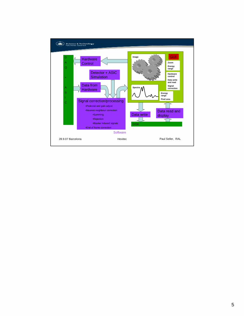
28.9.07 Barcelona Hexitec Paul Seller, RAL
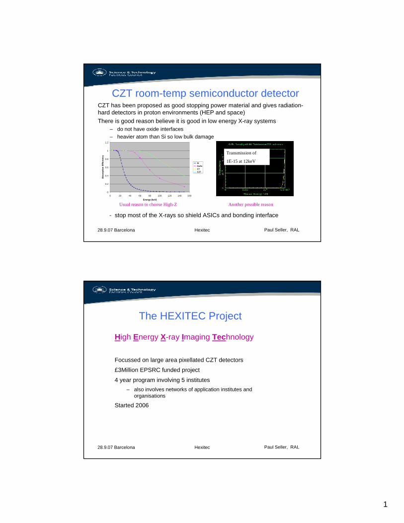
CZT room-temp semiconductor detectorCZT has been proposed as good stopping power material and gives radiation-hard detectors in proton environments (HEP and space)There is good reason believe it is good in low energy X-ray systems
– do not have oxide interfaces– heavier atom than Si so low bulk damage
Transmission of
1E-15 at 12keV
0
0.2
0.4
0.6
0.8
1
1.2
0 20 40 60 80 100 120 140 160
Energy (keV)
Ab
sorp
tio
n E
ffic
ien
cy
SiGaAsCTCZT
Usual reason to choose High-Z Another possible reason
- stop most of the X-rays so shield ASICs and bonding interface
28.9.07 Barcelona Hexitec Paul Seller, RAL
High Energy X-ray Imaging Technology
Focussed on large area pixellated CZT detectors
£3Million EPSRC funded project
4 year program involving 5 institutes
– also involves networks of application institutes and organisations
Started 2006
The HEXITEC Project
2
28.9.07 Barcelona Hexitec Paul Seller, RAL
HEXITEC Project objectives
fabricate large area CZT detector material for X-ray imaging
characterise to improvement material performance
develop cutting/polishing/contact-deposition and passivation techniques
develop bump-bonding techniques for CZT
develop pixellated spectroscopy ASIC for CZT
insert this technology into a diverse network of scientific users
create a sustainable base for continued CZT detector production
28.9.07 Barcelona Hexitec Paul Seller, RAL
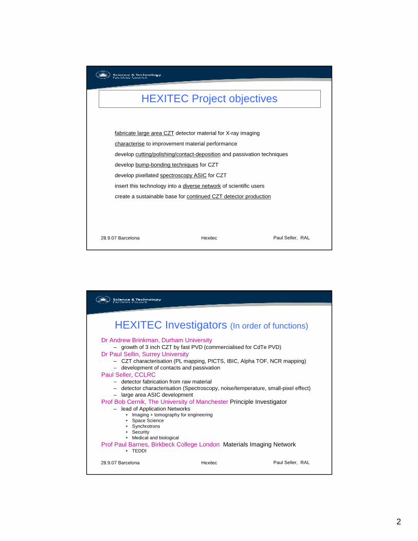
Dr Andrew Brinkman, Durham University– growth of 3 inch CZT by fast PVD (commercialised for CdTe PVD)
Dr Paul Sellin, Surrey University– CZT characterisation (PL mapping, PICTS, IBIC, Alpha TOF, NCR mapping)– development of contacts and passivation
Paul Seller, CCLRC– detector fabrication from raw material– detector characterisation (Spectroscopy, noise/temperature, small-pixel effect)– large area ASIC development
Prof Bob Cernik, The University of Manchester Principle Investigator– lead of Application Networks
• Imaging + tomography for engineering• Space Science• Synchrotrons• Security• Medical and biological
Prof Paul Barnes, Birkbeck College London Materials Imaging Network • TEDDI
HEXITEC Investigators (In order of functions)
3
28.9.07 Barcelona Hexitec Paul Seller, RAL
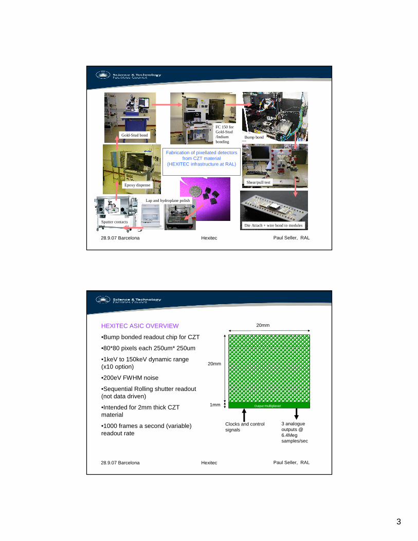
Fabrication of pixellated detectors from CZT material
(HEXITEC infrastructure at RAL)
Gold-Stud bond Bump bond
Shear/pull test
FC 150 for Gold-Stud /Indium bonding
Die Attach + wire bond to modules
Epoxy dispense
Lap and hydroplane polish
Sputter contacts
28.9.07 Barcelona Hexitec Paul Seller, RAL
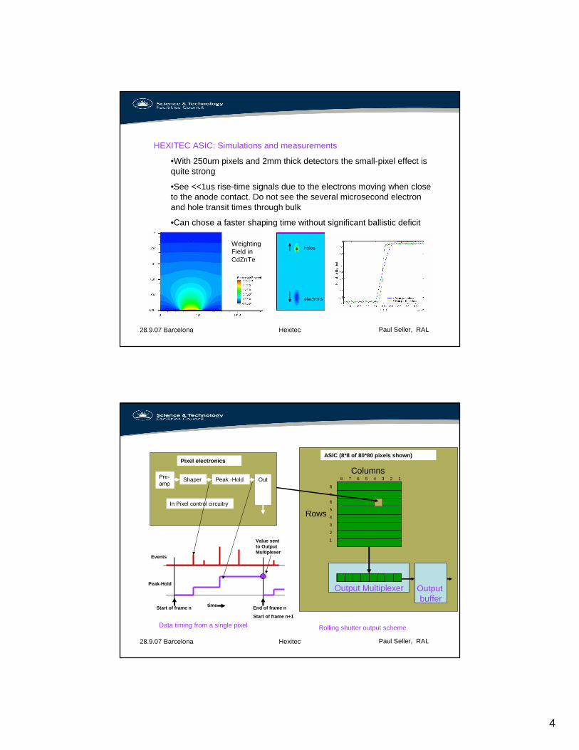
HEXITEC ASIC OVERVIEW
•Bump bonded readout chip for CZT
•80*80 pixels each 250um* 250um
•1keV to 150keV dynamic range (x10 option)
•200eV FWHM noise
•Sequential Rolling shutter readout (not data driven)
•Intended for 2mm thick CZT material
•1000 frames a second (variable) readout rate
Clocks and control signals
3 analogue outputs @ 6.4Meg samples/sec
Output multiplexer
20mm
1mm
20mm
4
28.9.07 Barcelona Hexitec Paul Seller, RAL
HEXITEC ASIC: Simulations and measurements
•With 250um pixels and 2mm thick detectors the small-pixel effect is quite strong
•See <<1us rise-time signals due to the electrons moving when close to the anode contact. Do not see the several microsecond electron and hole transit times through bulk
•Can chose a faster shaping time without significant ballistic deficit
Weighting Field in CdZnTe
electrons
holes
28.9.07 Barcelona Hexitec Paul Seller, RAL
OutPre-amp
Shaper
Pixel electronics
Peak -Hold
Value sent to Output Multiplexer
Start of frame n End of frame n
Start of frame n+1
Peak-Hold
Events
Data timing from a single pixel
time
In Pixel control circuitry
Output buffer
Output Multiplexer
8
7
6
5
4
3
2
1
8 7 6 5 4 3 2 1
Columns
Rows
Rolling shutter output scheme
ASIC (8*8 of 80*80 pixels shown)
5
28.9.07 Barcelona Hexitec Paul Seller, RAL
Software
Data write
GUI
Data read and display
Zoom
Energy range
Signal correction/processing•Pedestal and gain adjust
•Nearest neighbour correction
•Summing
•Rejection
•Bipolar induced signals
•End of frame correction
Data from Hardware
Hardware Control
D
A
Q
+
A
S
I
C
DISK
Energy range
Pixel area
Hardware control
Data write and read
Signal correctionSpectra
Image
Detector + ASIC Simulation