semiconductor detectorsatlas.physics.arizona.edu/~shupe/physics_courses/phys_586_s2015_s...1...
TRANSCRIPT
1
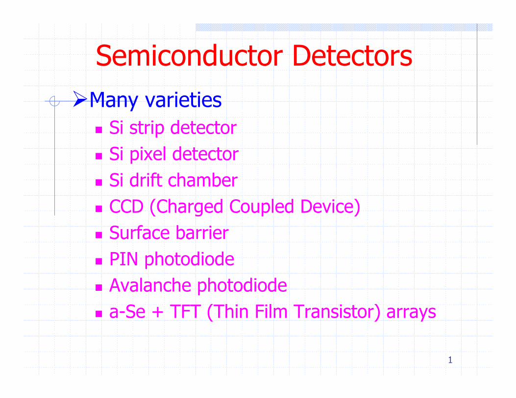
Semiconductor DetectorsMany varieties
Si strip detectorSi pixel detectorSi drift chamberCCD (Charged Coupled Device) Surface barrier PIN photodiodeAvalanche photodiodea-Se + TFT (Thin Film Transistor) arrays
2
PhotodiodesPhotodiodes are semiconductor detectors that convert light into an electric current
Also responsive to charged particlesUsed in a wide variety of applications in science and commercially
All p-n junctions (diodes) are light sensitivePhotodiodes are designed to optimize this effect

3
Photodiodes
4
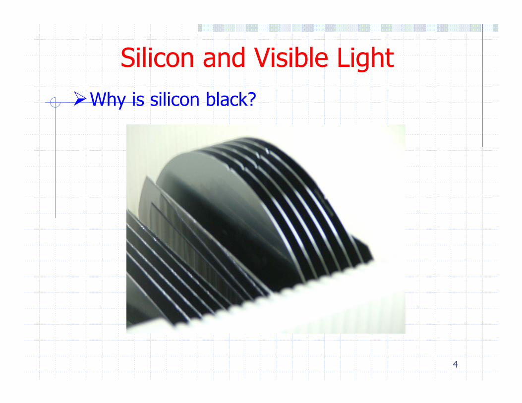
Silicon and Visible LightWhy is silicon black?
5
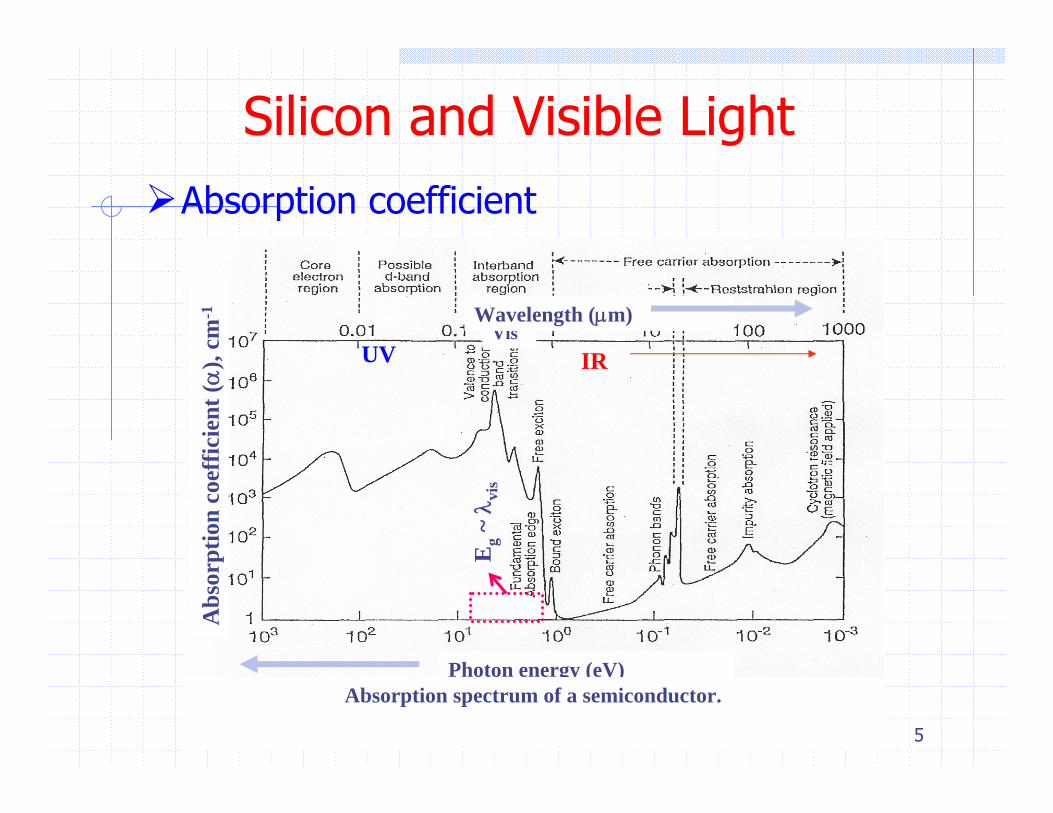
Silicon and Visible LightAbsorption coefficientA
bsor
ptio
n co
effic
ient
(α),
cm-1
Photon energy (eV)Absorption spectrum of a semiconductor.
Vis
Eg
~ λ vi
s
Wavelength (μm)
IRUV
6
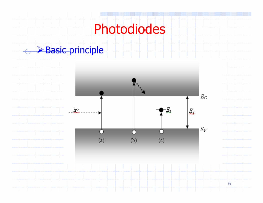
PhotodiodesBasic principle
7
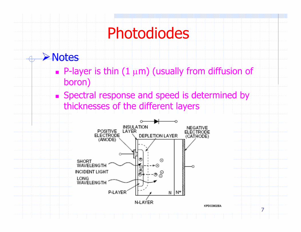
PhotodiodesNotes
P-layer is thin (1 μm) (usually from diffusion of boron)Spectral response and speed is determined by thicknesses of the different layers
8
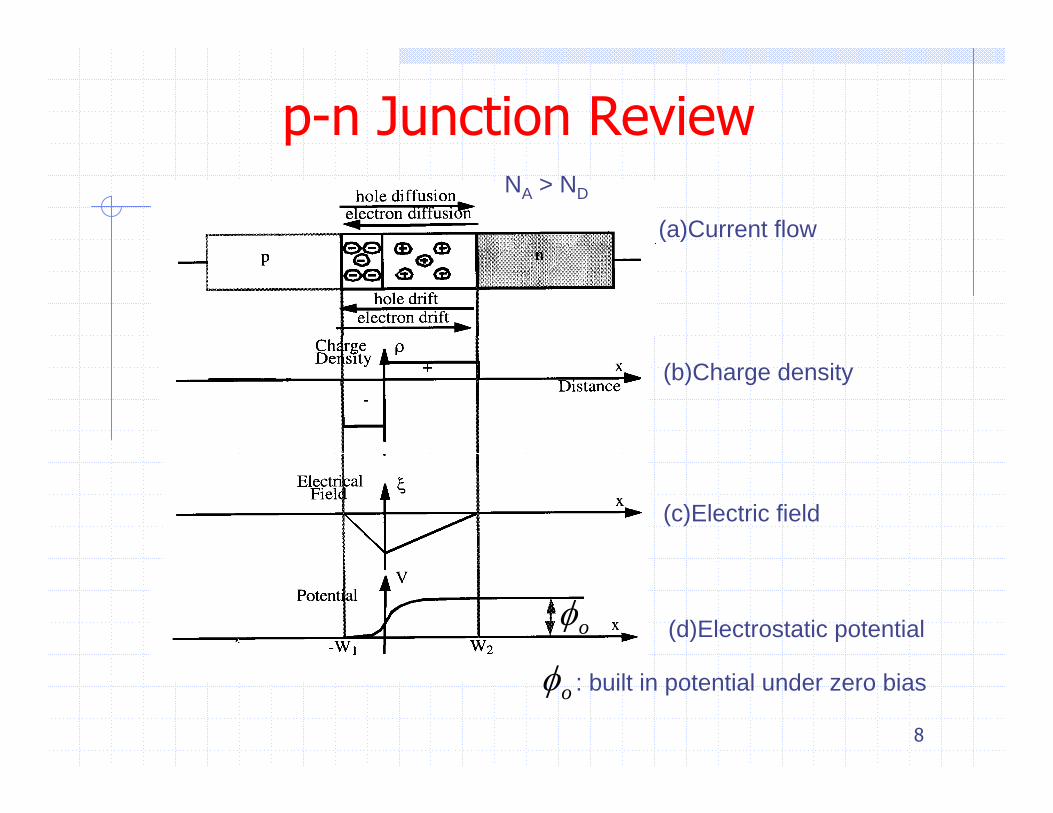
p-n Junction Review
(a)Current flow
(c)Electric field
(b)Charge density
NA > ND
(d)Electrostatic potential
oφ : built in potential under zero bias
oφ
9
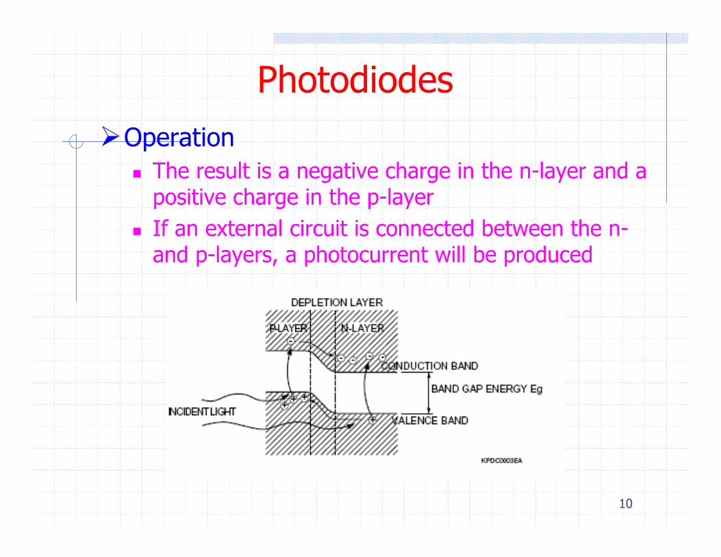
PhotodiodesOperation
Electron-hole pairs are created throughout the photodiodeThose in the depletion layer are accelerated to their respective sides (electrons to n, holes to p)Electrons generated in the n-layer, along with diffusion electrons from the p-layer, are left in the conduction bandHoles generated in the n-layer diffuse to the depletion layer and are collected in the p-layer valance bandOf course, some of the charge carriers created outside the depletion region will recombine and disappear
10
PhotodiodesOperation
The result is a negative charge in the n-layer and a positive charge in the p-layerIf an external circuit is connected between the n-and p-layers, a photocurrent will be produced
11
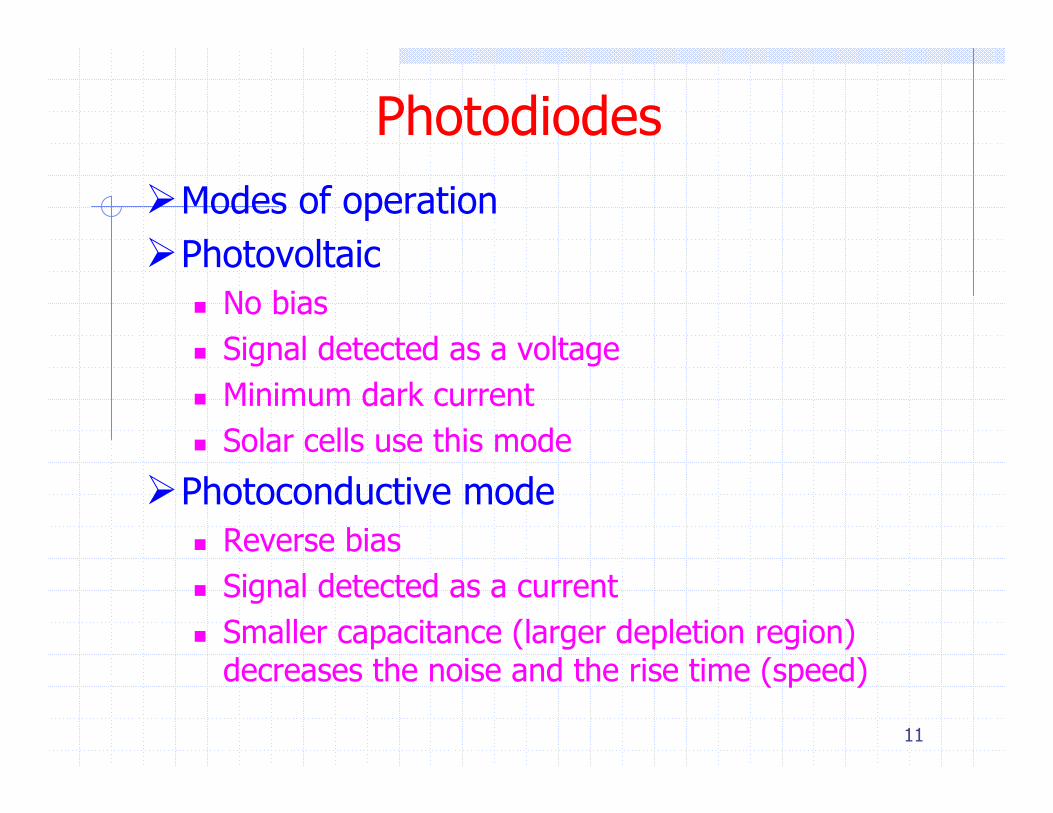
PhotodiodesModes of operationPhotovoltaic
No biasSignal detected as a voltageMinimum dark currentSolar cells use this mode
Photoconductive modeReverse biasSignal detected as a currentSmaller capacitance (larger depletion region) decreases the noise and the rise time (speed)
12
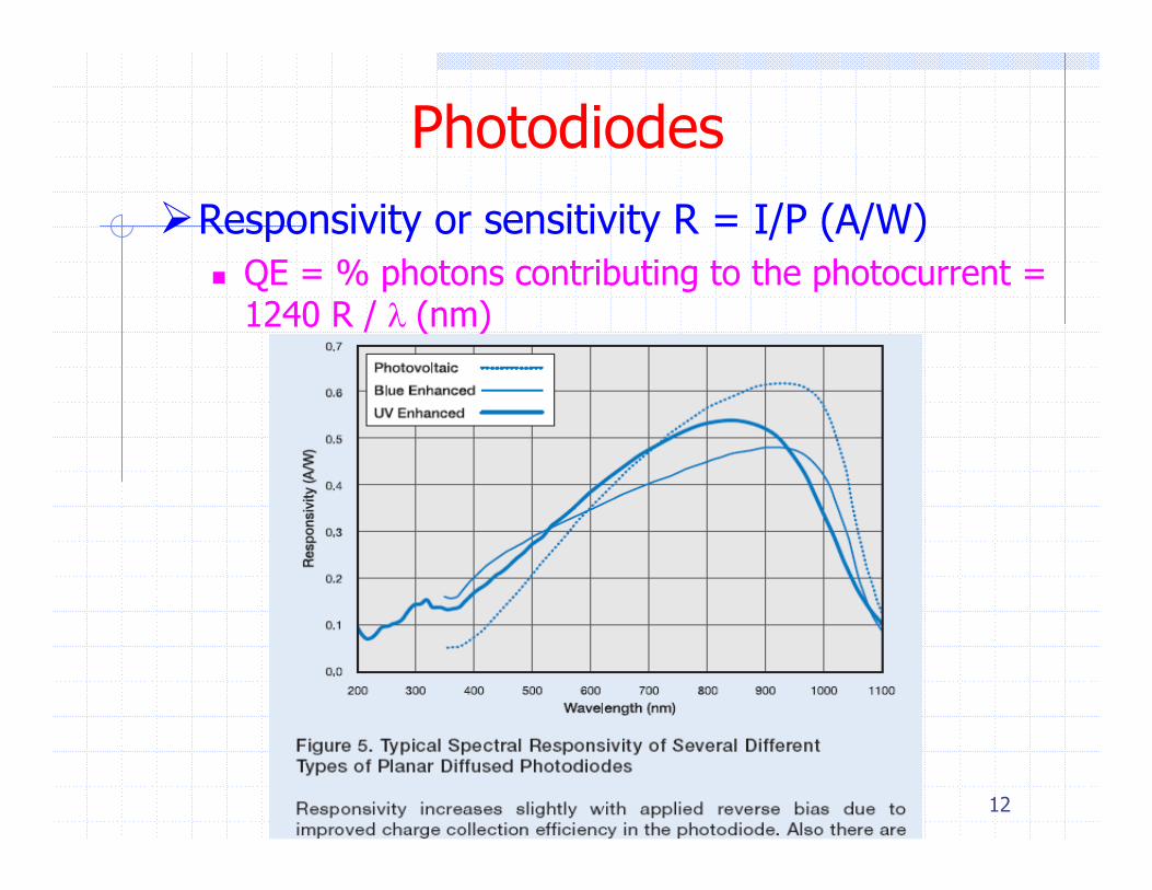
PhotodiodesResponsivity or sensitivity R = I/P (A/W)
QE = % photons contributing to the photocurrent = 1240 R / λ (nm)
13
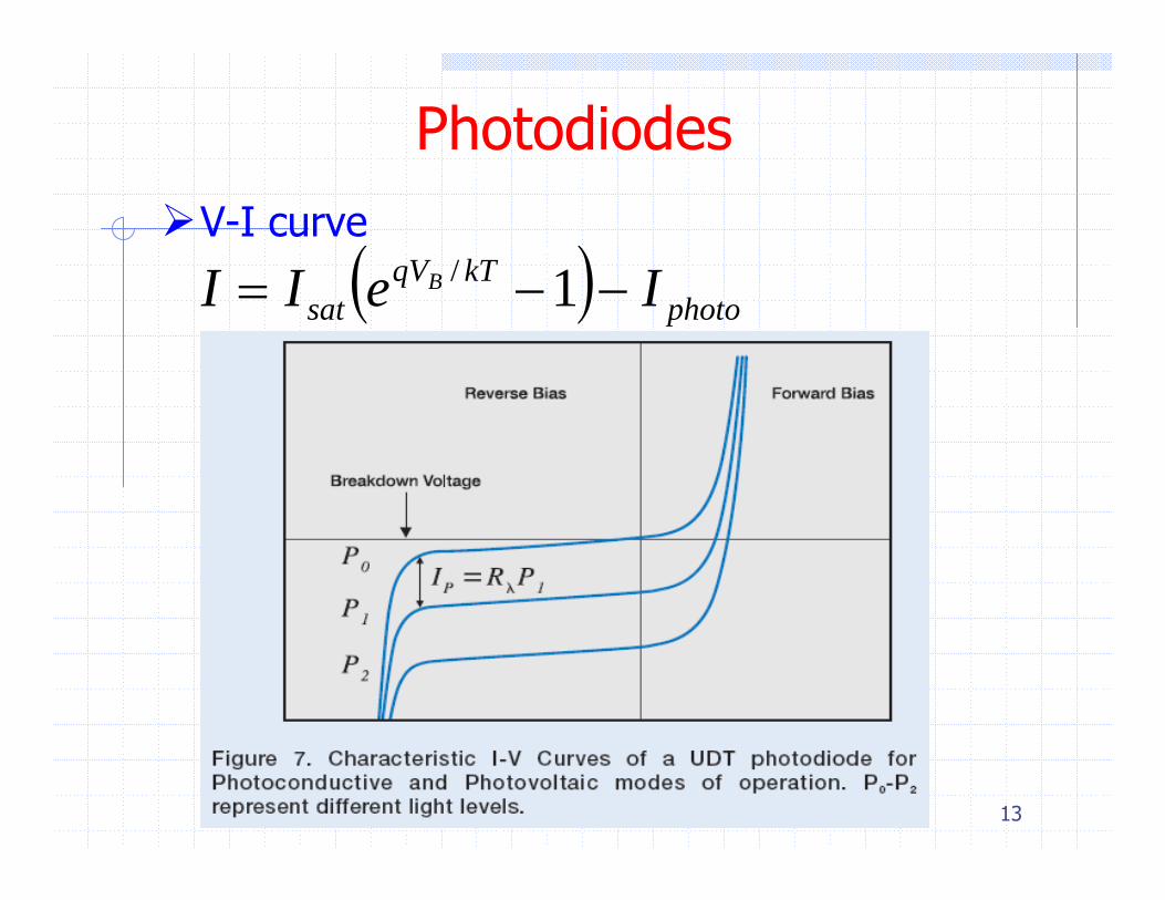
PhotodiodesV-I curve
( ) photokTqV
sat IeII B −−= 1/
14
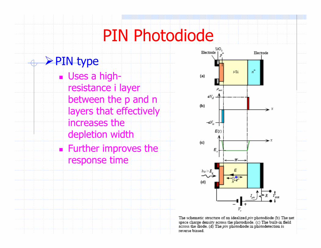
PIN PhotodiodePIN type
Uses a high-resistance i layer between the p and n layers that effectively increases the depletion widthFurther improves the response time
15
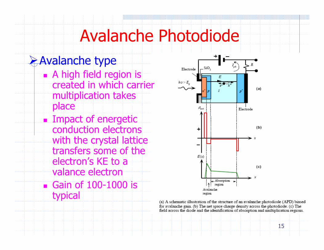
Avalanche PhotodiodeAvalanche type
A high field region is created in which carrier multiplication takes place Impact of energetic conduction electrons with the crystal lattice transfers some of the electron’s KE to a valance electronGain of 100-1000 is typical
16
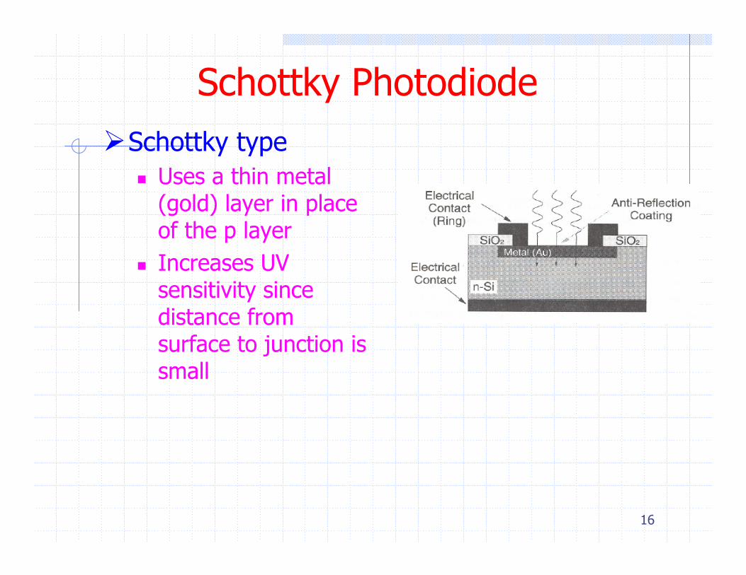
Schottky PhotodiodeSchottky type
Uses a thin metal (gold) layer in place of the p layerIncreases UV sensitivity since distance from surface to junction is small
17
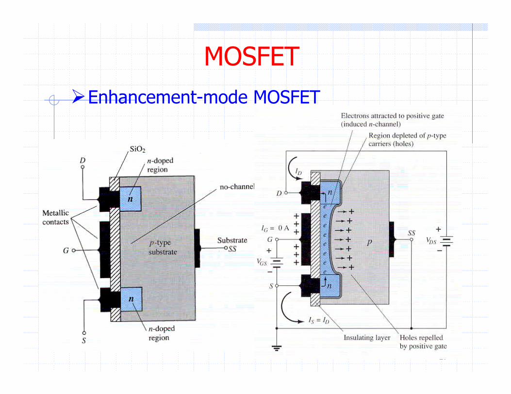
MOSFETEnhancement-mode MOSFET
18
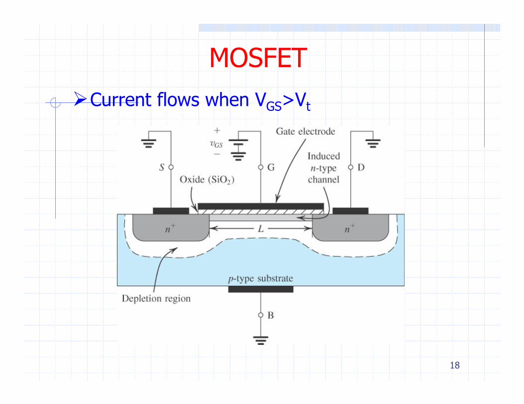
MOSFETCurrent flows when VGS>Vt
19
MOSFETConnecting a small voltage to the gate Vgs(relative to the source, and thus the substrate), attracts electrons to the gateThe oxide insulation prevents current from entering the gate and forms a parallel plate capacitorThese electrons induce an n-type region called a channel
This is called an NMOS transistorThe value required to form the conducting channel is called the threshold voltage and is denoted Vt

20
MOSFET
Characteristic I-V curve
21
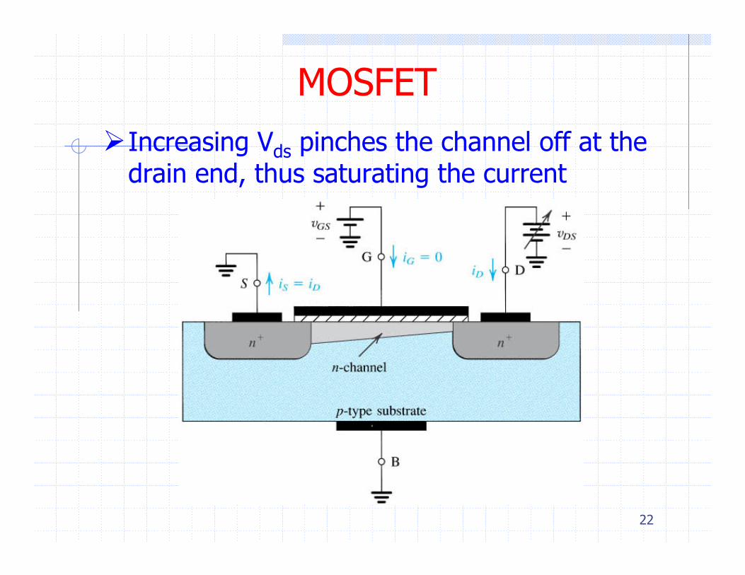
MOSFETApplying a small (~50 mV) Vds will cause current (electrons) to flow from source to drain
The NMOS transistor is essentially a transistor here
Increasing Vgs > Vt attracts more electrons to the channel thus decreasing the resistance and increasing the currentIncreasing Vds further such that Vgd=Vtdecreases the channel depth to almost zero
The channel is pinched off and the drain current saturates
22
MOSFETIncreasing Vds pinches the channel off at the drain end, thus saturating the current
23
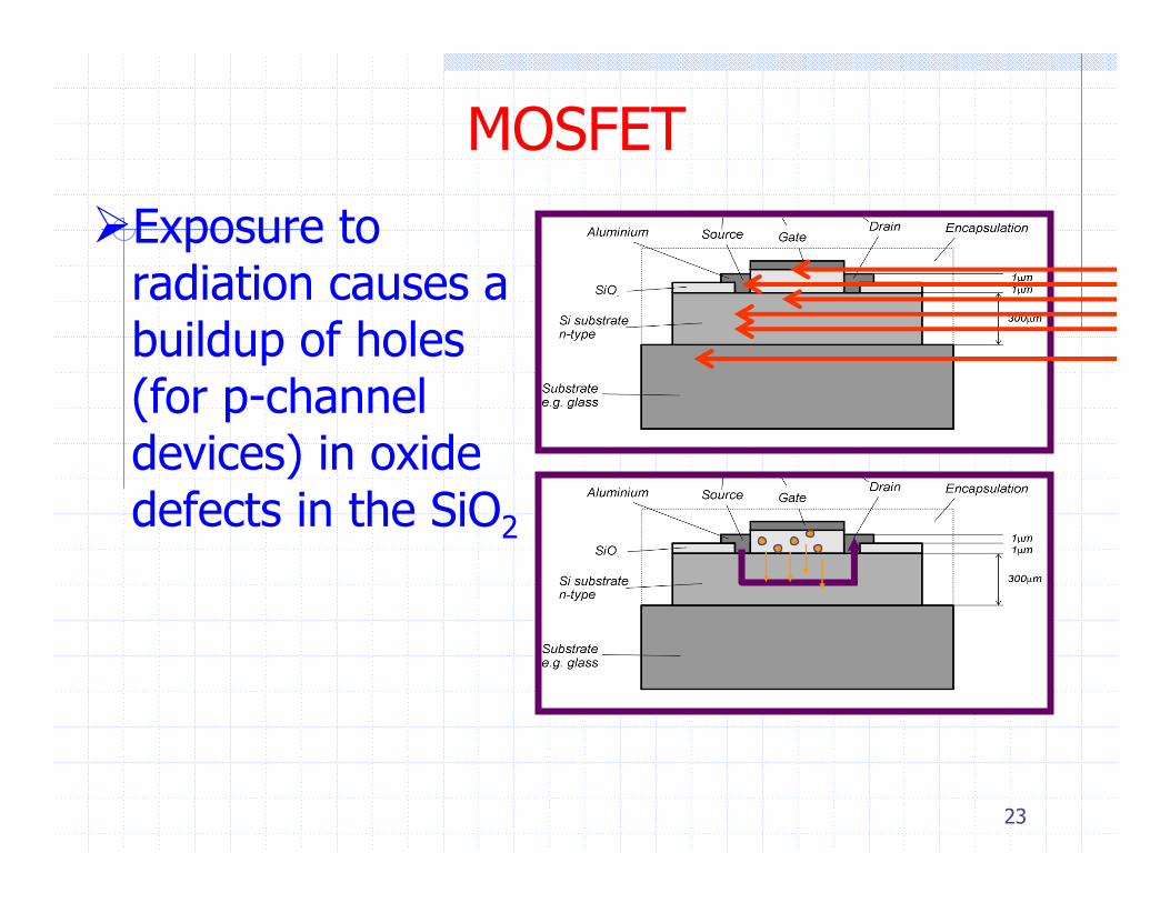
MOSFET
Exposure to radiation causes a buildup of holes (for p-channel devices) in oxide defects in the SiO2
24
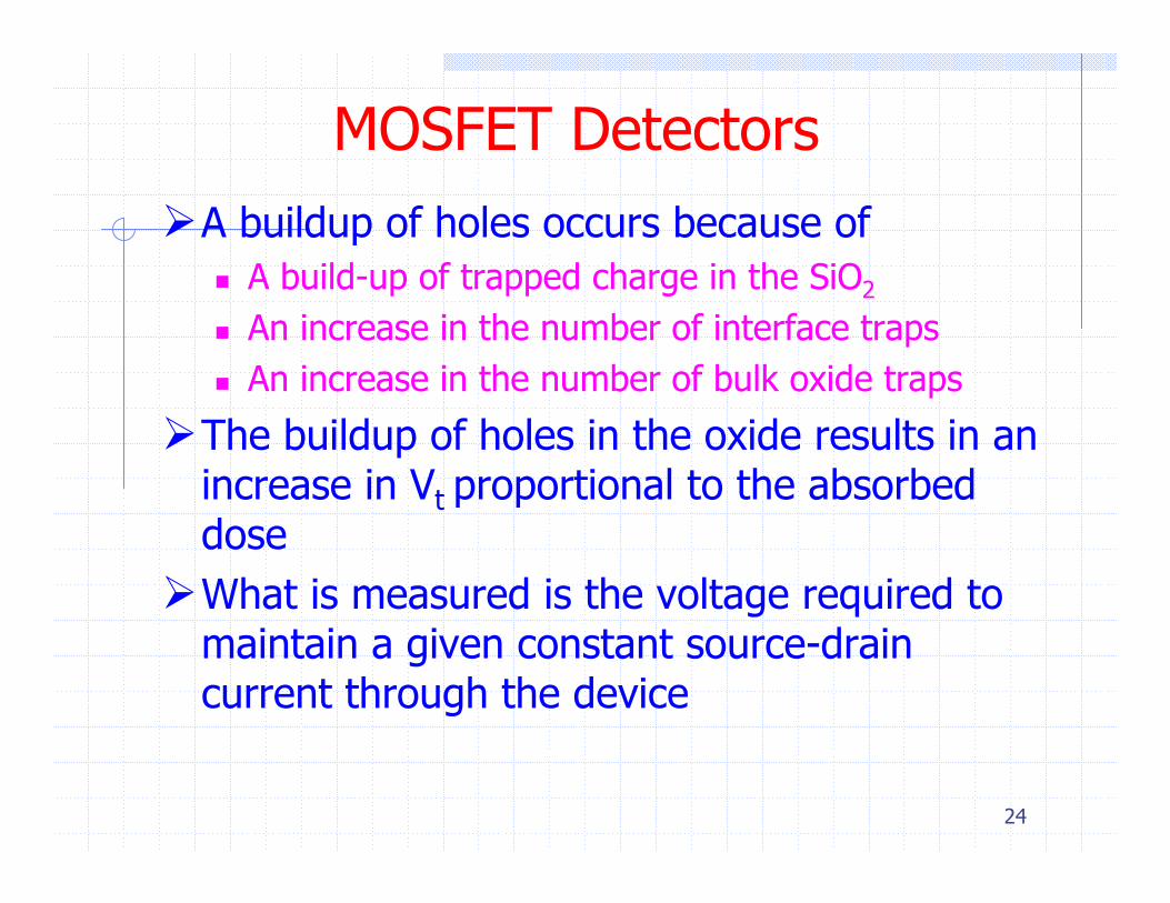
MOSFET DetectorsA buildup of holes occurs because of
A build-up of trapped charge in the SiO2
An increase in the number of interface trapsAn increase in the number of bulk oxide traps
The buildup of holes in the oxide results in an increase in Vt proportional to the absorbed doseWhat is measured is the voltage required to maintain a given constant source-drain current through the device

25
MOSFET Detectors
26
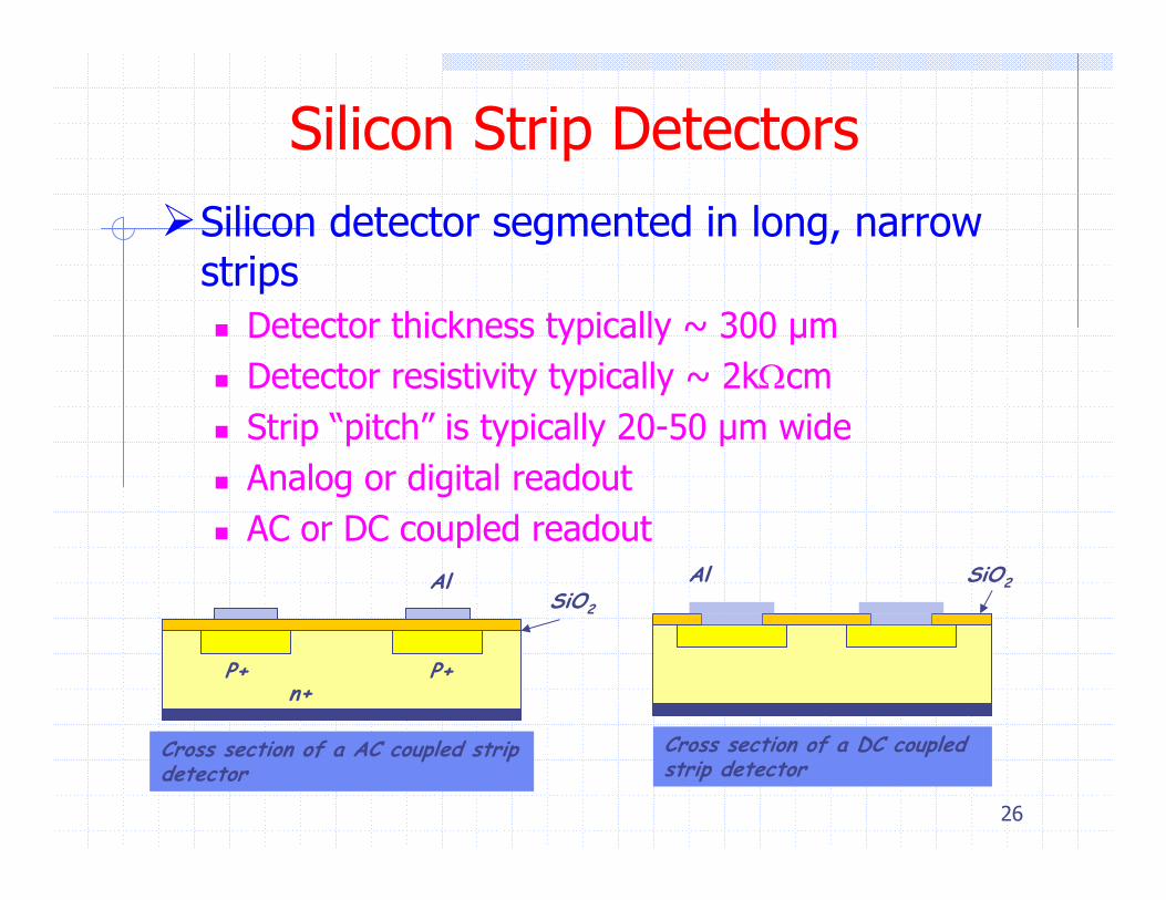
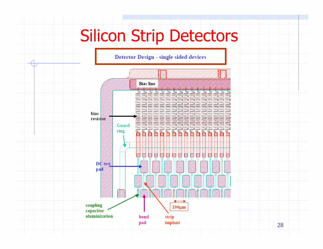
Silicon Strip DetectorsSilicon detector segmented in long, narrow strips
Detector thickness typically ~ 300 μmDetector resistivity typically ~ 2kΩcmStrip “pitch” is typically 20-50 μm wideAnalog or digital readoutAC or DC coupled readout
P+n+
Al
P+
Cross section of a AC coupled strip detector
SiO2
Cross section of a DC coupled strip detector
Al SiO2

27
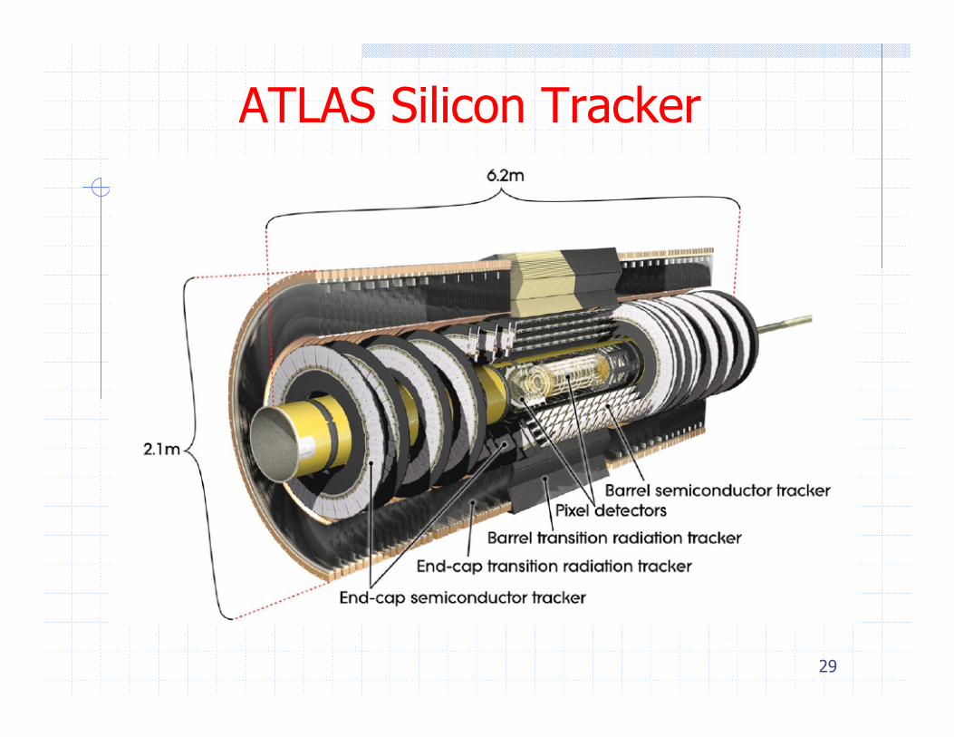
ATLAS Silicon Tracker (SCT)
28
Silicon Strip Detectors
29
ATLAS Silicon Tracker
30
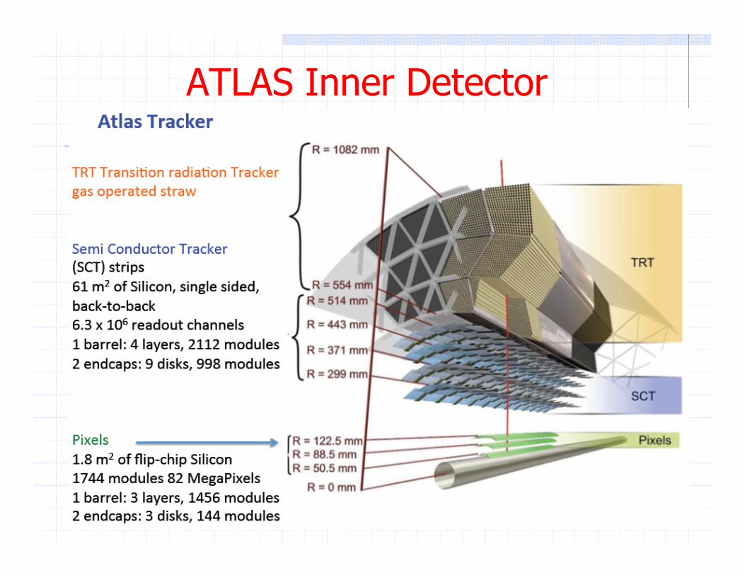
ATLAS Inner Detector

31
ATLAS Silicon Tracker
32
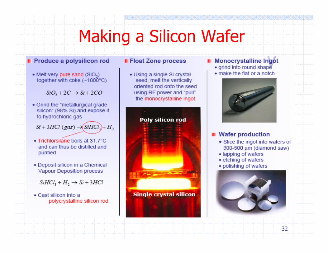
Making a Silicon Wafer
33
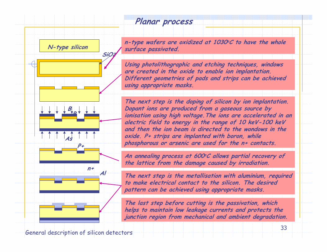
Planar process
General description of silicon detectors
N-type siliconSiO2
BB
As
n+
P+
n-type wafers are oxidized at 1030oC to have the whole surface passivated.
Using photolithographic and etching techniques, windows are created in the oxide to enable ion implantation. Different geometries of pads and strips can be achieved using appropriate masks.
The next step is the doping of silicon by ion implantation. Dopant ions are produced from a gaseous source by ionisation using high voltage.The ions are accelerated in an alectric field to energy in the range of 10 keV-100 keVand then the ion beam is directed to the wondows in the oxide. P+ strips are implanted with boron, while phosphorous or arsenic are used for the n+ contacts.
An annealing process at 600oC allows partial recovery of the lattice from the damage caused by irradiation.
The next step is the metallisation with aluminium, required to make electrical contact to the silicon. The desired pattern can be achieved using appropriate masks.
Al
The last step before cutting is the passivation, which helps to maintain low leakage currents and protects the junction region from mechanical and ambient degradation.