ionic cooling systemd2oqb2vjj999su.cloudfront.net/users/000/084/887/729... · the ionic cooling...
TRANSCRIPT
Page | i
Ionic Cooling System
EML 4551 - Senior Design Project
Team 9
Patrick Burgart - Aaron Hearnz - Lucas Harris
Cover Page
Advisor:
Dr. Masory
December 11, 2013

Page | ii
© 2013, Team 9 and Florida Atlantic University

Page | iii
ABSTRACT
The Ionic Cooling System is a smart alternative to the conventional methods of cooling
electronics. The ICS replaces the standard fan by providing the needed air flow to keep the
internal components of electronics at proper operating temperatures. The systems works by
utilizing the corona effect to ionize air to create bulk airflow in the system.
The system consists of four major components which drive the system. A high voltage
power supply is created to create the corona discharge needed for operation. A system of
collector and emitter units will control the direction of the airflow. The heat sink and enclosure
unit will be built to house the electrical components and show the heat convection ability of the
device. A temperature feedback system will be built to control the flow of the system based on
variable heating loads.
The device is meant for microelectronic applications, so size and power consumption
were of major priority. Work was done to create a small and modular case and heat sink
structure, and further improvement in this area could minimize the footprint further. Power
consumption in the system was extremely small with only 1.56W measured while the system is
running. The actual underlying ionic circuitry pulls much less power due to the LCD screen and
Ardiuno circuitry that the prototype used for operation
The results of the project were mixed. The team’s circuitry failed to deliver the voltage
that was originally stipulated in the design proposal. The device’s airflow had a high enough
velocity to blow out a lighter flame during test. During testing a malfunction in the system
prevented further data to be collected. Ultimately, further work can be done to improve upon this
prototype design, and with proper funding a marketable version of the device can be made.

Page | iv
Table of Contents
COVER PAGE ................................................................................................................................. I
ABSTRACT .................................................................................................................................... III
LIST OF FIGURES ........................................................................................................................ VI
LIST OF TABLES ........................................................................................................................... VI
1 INTRODUCTION ........................................................................................................................ 7
1.1 PROBLEM STATEMENT ...................................................................................................... 7 1.2 TECHNICAL REVIEW .......................................................................................................... 7
1.2.1 Corona Discharge ................................................................................................... 8 1.2.2 Onset Voltage ......................................................................................................... 9
1.2.3 Feasibility of electrostatic airflow. ........................................................................... 9
2 DESIGN DESCRIPTION .......................................................................................................... 11 2.1 OVERVIEW ...................................................................................................................... 11 2.2 DETAILED DESCRIPTION .................................................................................................. 12
2.2.1 High Voltage power Supply .................................................................................. 12 2.2.2 Modified H-bridge .................................................................................................. 13 2.2.3 Transformer ........................................................................................................... 14
2.2.4 Capacitor Bank ..................................................................................................... 14 2.2.5 Design and implement the Emitter and Collector System ................................... 15 2.2.6 Case Design and Heat sink .................................................................................. 16 2.2.7 Case – shape and fitting ....................................................................................... 17
2.2.8 Feedback control .................................................................................................. 17 2.2.9 Voltage Probe ....................................................................................................... 18 2.2.10 Arduino Screen Output ......................................................................................... 18
2.3 USE ................................................................................................................................ 19
3 EVALUATION........................................................................................................................... 20 3.1 OUTCOME ....................................................................................................................... 20 3.2 TESTING AND RESULTS ................................................................................................... 21
3.2.1 The high Voltage circuit ........................................................................................ 21
3.2.2 Power draw ........................................................................................................... 21 3.2.3 Emitter and Collector Units ................................................................................... 22 3.2.4 Damage to the circuit ............................................................................................ 22
4 DISCUSSION ........................................................................................................................... 23
4.1 ASSESSMENT .................................................................................................................. 23 4.2 NEXT STEPS ................................................................................................................... 24
5 CONCLUSION ......................................................................................................................... 25
REFERENCES ............................................................................................................................. 26
A P P E N D I X ............................................................................................................................. 27
Page | v
Appendix A: Drawing – Insulator .......................................................................................... 28 Appendix B: Drawing – Insulator End Fin ............................................................................ 29
Appendix C: Drawing – Insulator Floor ................................................................................. 30 Appendix D: Drawing – Insulator Side Wall – Display.......................................................... 31 Appendix E: Drawing – Insulator Side Wall – Power ........................................................... 32 Appendix F: Drawing – Insulator Side Wall .......................................................................... 33
Appendix G: Drawing – Lid ................................................................................................... 34 Appendix H: Drawing – Heat Sink Fin .................................................................................. 35 Appendix I: Drawing – Heat Sink Spacer ............................................................................ 36 Appendix J: Drawing – Assembly ........................................................................................ 37
Appendix K: Exploded assembly view .................................................................................. 38 Appendix L: Probe testing data ............................................................................................ 39 Appendix M: Bill of Materials ................................................................................................. 40 Appendix N: Custom Built Transformer ............................................................................... 41

Page | vi
LIST OF FIGURES
Figure 1: Diagram of the corona effect ........................................................................................... 8 Figure 2: Block Diagram of overall system ................................................................................... 11 Figure 3: Flow chart of high voltage power supply ....................................................................... 12 Figure 4: Cockcroft walton Voltage multiplier diagram................................................................. 12
Figure 5: IR2010 Recommended circuit diagram ........................................................................ 13 Figure 6: Voltage Output vs number of stages............................................................................. 15 Figure 7: Slider unit for distance testing ....................................................................................... 16
Figure 8: Collector and emitter diagram ....................................................................................... 16 Figure 9: Completed case assembly ............................................................................................ 17 Figure 11: Voltage Probe Schematic ............................................................................................ 18
LIST OF TABLES
Table 1: Evaluation outcomes ...................................................................................................... 20 Table 2: Power consumption and voltage consumption for transformer ..................................... 21 Table 3: Table of power consumption for the device ................................................................... 21

Page | 7
1 INTRODUCTION
1.1 Problem Statement
The ever-advancing developments in electronics require new methods of cooling. Thermal
management of microelectronics, due to counterpart advancements, becomes the limiting agent
in overall evolution. Immense component density, contributing to heightening performance,
remains threatened by conventional cooling methods. Optimization for the rotary fan is
restricted, due to moving parts, and static cross-sectional air velocity profiles. Ionic cooling, in
the form of an ionic wind pump, is set at an advantage due to its nature and advancing field of
study, research, and development. Lack of moving parts, controllable air propulsion velocities,
and dynamic airflow profiles have become attractive features offered by the advancement of
ionic cooling. The ionic wind pump has room in thermal management where conventional
methods cannot apply.
The ionic wind pump, or fan, works on a principle that is similar to the Corona Effect. The
Corona Effect is a physics principle that, when achieved, provides air propulsion between a
high-voltage emitter and collector. The result is due to ionized air created in an intense electric
field from the voltage difference. Early recorded observations of the corona effect date back
those whom pioneered the field in the study of electricity. It is known that lightning is a natural
atmospheric coolant; and ionic wind cooling is currently making advancements in the
development of technologies that provide ozone depletion, air purification, and air conditioning.
The ionic wind pump is a stand-alone thermal cooling device, and will be a prototype of an ionic
fan that could eventually be embedded inside of small electronics.
1.2 Technical Review
The ionic cooler proposed in this report works off the principle of electro-hydrodynamics.
The mechanism of action within the cooler is that a high voltage DC source is sent through
small sharp tip object called the emitter. The high voltage current ionizes the air within the
vicinity of the emitter tip leading to a Corona discharge of the electrons. The now ionized air is
then propelled by electric field that extends from emitter tip to a common ground (collector)
electrode located downstream from the electrode. The movement of the ionized air to the
collector causes bulk airflow as the ionized air exchanges its momentum in the stream [1].
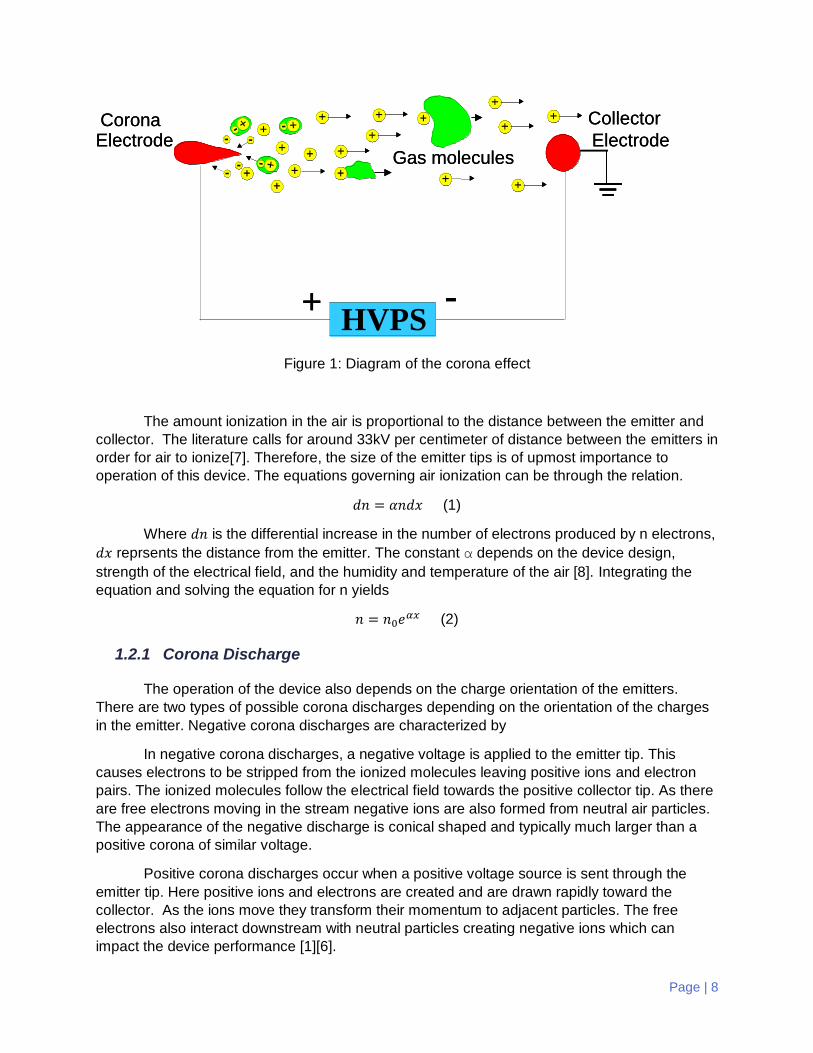
Page | 8
Figure 1: Diagram of the corona effect
The amount ionization in the air is proportional to the distance between the emitter and
collector. The literature calls for around 33kV per centimeter of distance between the emitters in
order for air to ionize[7]. Therefore, the size of the emitter tips is of upmost importance to
operation of this device. The equations governing air ionization can be through the relation.
(1)
Where is the differential increase in the number of electrons produced by n electrons,
reprsents the distance from the emitter. The constant α depends on the device design,
strength of the electrical field, and the humidity and temperature of the air [8]. Integrating the
equation and solving the equation for n yields
(2)
1.2.1 Corona Discharge
The operation of the device also depends on the charge orientation of the emitters.
There are two types of possible corona discharges depending on the orientation of the charges
in the emitter. Negative corona discharges are characterized by
In negative corona discharges, a negative voltage is applied to the emitter tip. This
causes electrons to be stripped from the ionized molecules leaving positive ions and electron
pairs. The ionized molecules follow the electrical field towards the positive collector tip. As there
are free electrons moving in the stream negative ions are also formed from neutral air particles.
The appearance of the negative discharge is conical shaped and typically much larger than a
positive corona of similar voltage.
Positive corona discharges occur when a positive voltage source is sent through the
emitter tip. Here positive ions and electrons are created and are drawn rapidly toward the
collector. As the ions move they transform their momentum to adjacent particles. The free
electrons also interact downstream with neutral particles creating negative ions which can
impact the device performance [1][6].
HVPSHVPS
Collector
ElectrodeGas molecules
CoronaElectrode
- +
HVPSHVPS
Collector
ElectrodeGas molecules
CoronaElectrode
- +

Page | 9
1.2.2 Onset Voltage
The voltage needed for onset ionization can be described for a wire to plate
configuration using Peek’s law [6]. Peek’s law defines the minimum electrical potential needed
to initiate a corona discharge between two wires. The equation is given by:
(
√ ) (3)
Where the electric field on the wire is given in terms of the voltage potential:
0
0
2ln
wireEd
rr
(4)
The substitution of 3 and 4 yields
2
0 0
00
00301 21 . lnc v
dE m r
rr
(5)
The equation above describes the voltage potential needed for a corona discharge
based off of the operating conditions. is the critical potential gradient for air which is around
33kV/cm for standard air. The factor vm is scaling factor that accounts for impurities in the wire
tip. is the gas density factor for air.
From fluid dynamic modeling the pressure drop across the wire gap between the emitter
and collector can be given as:
0
2ln
i d dp
b A r
(6)
Where I is the current, d is the distance between the emitter and the collector, A is the
area of the collector, and 0r is the radius of the emitter. The pressure drop can be then be
related to the voltage potential of the device through substitution. The constant b is the ion
mobility factor and is related to the temperature of the air.
The equation (6) allows for the current information to be written in terms of the pressure
drop across the emitter. This allows for a fairly straightforward fluid analysis to be conducted on
the channel.
1.2.3 Feasibility of electrostatic airflow.
Previous research on electrostatic airflow devices has produced mixed results. In the
early 1960’s Robinson, [1][9] studied the effect of corona driven ionic pumps. The studied
showed corona discharges only being about 1-2% efficient in converting electrical energy to
kinetic energy. Later studies focused on miniaturization have given more promises results.

Page | 10
Micro fabricated electrodes with radiuses on the order of 100µm drastically lower the necessary
voltage needed to engage a corona discharge [2][3]. As the onset voltage of the corona
discharge is related to the emitter tip radius and the gap distance, decreasing these parameters
improves the efficiency of the devices.
Various studies have been conducted on the feasibility of micro fabricated ionic device.
Researchers from the University of Washington have conducted multiple studies on electrostatic
coolers. The work conducted has looked into both negative and positive corona discharge
coolers along with various different types of emitter and collector geometries. Tessera
technologies Inc, which formed from the research at the University of Washington, produced a
prototype design of an ionic cooled laptop [2][3][4][6]. The research of both entities showed
comparable airflow and cooling properties to typical fans.
Purdue University looked at the combination of ionic cooling technology combined
typical fan air flow. The work performed showed a 50% increase in heat convective ability by the
cooler. Their work used extremely small size emitter tips with relatively low voltage. The
research show that the airflow is effected not only by the bulk air flow increase caused by the
ionic air flow, but also by the change in the velocity gradient due to the electromagnetic field
produced to ionize the air [10].
Page | 11
2 DESIGN DESCRIPTION
2.1 Overview
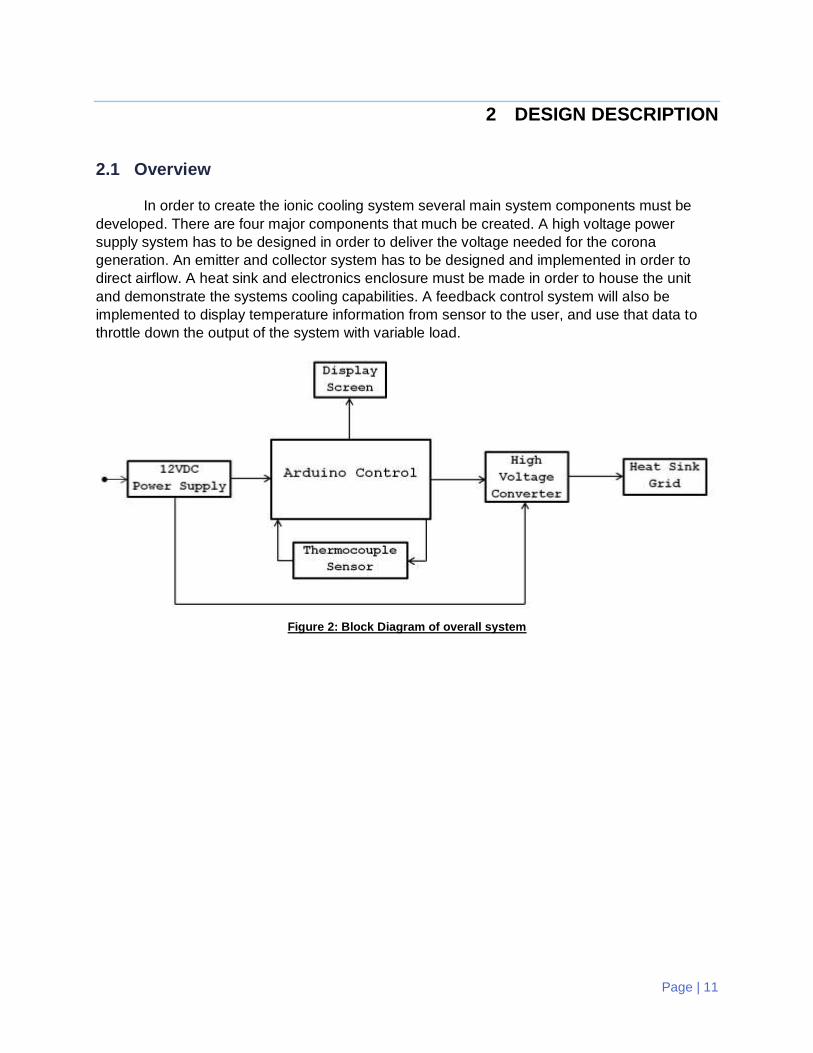
In order to create the ionic cooling system several main system components must be
developed. There are four major components that much be created. A high voltage power
supply system has to be designed in order to deliver the voltage needed for the corona
generation. An emitter and collector system has to be designed and implemented in order to
direct airflow. A heat sink and electronics enclosure must be made in order to house the unit
and demonstrate the systems cooling capabilities. A feedback control system will also be
implemented to display temperature information from sensor to the user, and use that data to
throttle down the output of the system with variable load.
Figure 2: Block Diagram of overall system

Page | 12
2.2 Detailed Description
2.2.1 High Voltage power Supply
The ionization of air only occurs under extremely high voltages (33kV/cm). In order to
produce a wind flow device delivering stable high voltage power is necessary for the function of
the device. The literature lists plenty of ways to create a high voltage power supply delivering a
constant DC voltage. The one most applicable to the project is a Cockcroft Walton Generator.
This takes in an AC current and uses a capacitor and diode ladder to increase the voltage within
the current. Various studies and documentation exist on this type of power supply. Most
literature indicates that ~10 stages of the ladder is needed to take a 200V AC voltage to 10kV
constant DC.
Figure 3: Flow chart of high voltage power supply
Figure 4: Cockcroft walton Voltage multiplier diagram
Creating the circuit necessary for this project required that we create the three
components that were needed for the voltage output. The modified H-bridge circuit exists to
change the unipolar PWM signal from the Arduino into a bipolar signal for use in the
transformer. An off the shelf transformer was originally used, but due to the high frequency of
the signal it was required that we build our own. Finally the capacitor bank is built from a
schematic of the Cockcroft voltage multiplier, but the number of stages and type of capacitors
used would need to be found experimentally.
Page | 13
2.2.2 Modified H-bridge
Two different designs were created by the team over the lifecycle of this product. The
first method using a low side driver in a push pull format was unsuccessful. The second method
used a high side driver and n-channel mosfets for improved efficiency and switch speed.
The first circuit used low side drivers to switch p-channel and n-channel mosfets with two
out of phase PWM waves. The out of phase PWM wave was created through using a from
SN7406 logic inverters to invert the square wave coming out of the ardiuno. The H-bridge circuit
was oriented with the p-channel mosfets going to the 12V line and the n-channel mosfets
connecting to the ground. The output of this circuit produced a modified bipolar square wave.
During testing of this circuit, it was noticed that the low side mosfet drivers were getting
extremely hot and their performance under these conditions began to decrease the longer the
unit was on. It was eventually realized that the combination of p-channel mosfets and n-channel
mosfets with the low side mosfets drivers was not an optimal setup. This circuit was eventually
scrapped due to these issues.
The second and successful circuit is essentially an h-bridge used for directional motor
control. This circuit features two low and high side moset drivers IR2010. These chips allow for
both low and high side output of the bridge, and also allow for us to use only n-channel mosfets.
Using only n-channel mosfet improves the efficieny and speed of the switching. Another benefit
was that we now had direct control over the voltage input on the high side of the bridge, given
that the high side mosfet drivers can be isolated from the rest of the chipset. This also meant
that during testing we could eliminate power to the high side of the circuit to protect the circuit
during testing.
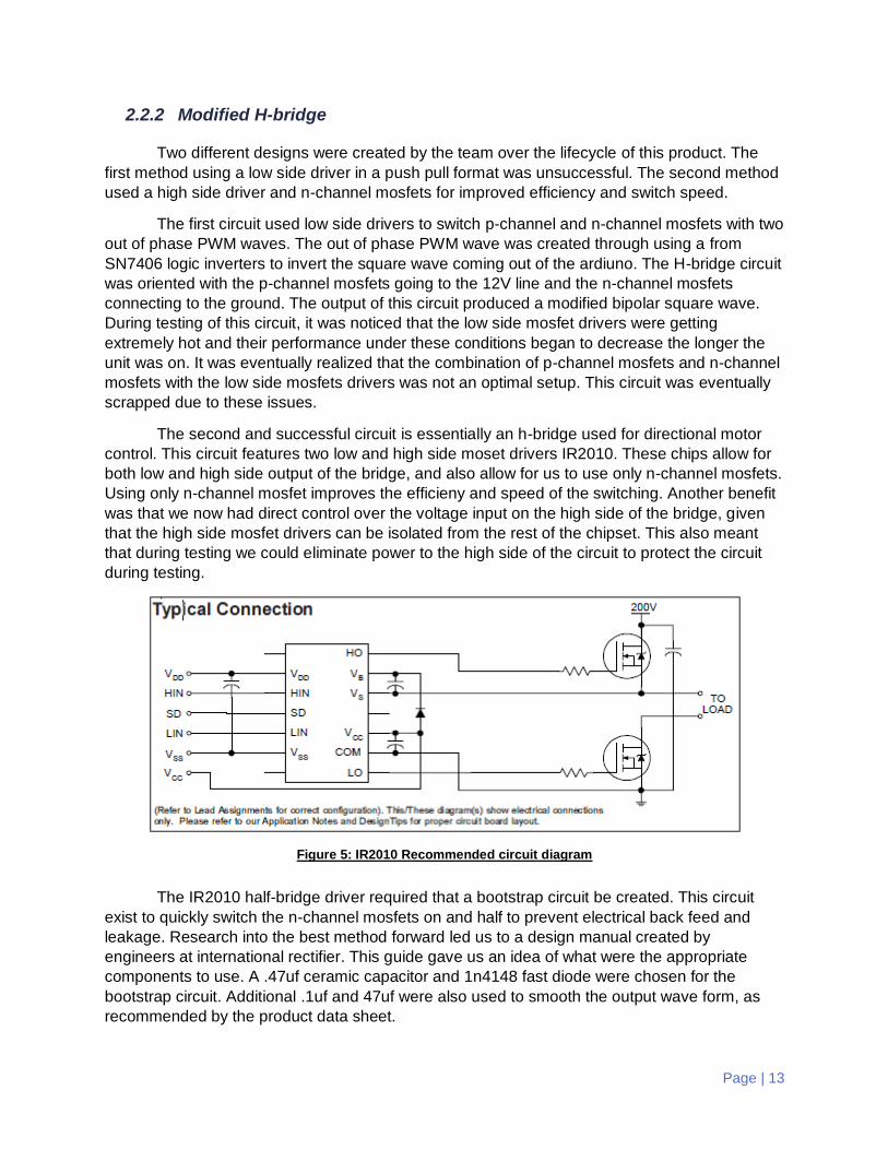
Figure 5: IR2010 Recommended circuit diagram
The IR2010 half-bridge driver required that a bootstrap circuit be created. This circuit
exist to quickly switch the n-channel mosfets on and half to prevent electrical back feed and
leakage. Research into the best method forward led us to a design manual created by
engineers at international rectifier. This guide gave us an idea of what were the appropriate
components to use. A .47uf ceramic capacitor and 1n4148 fast diode were chosen for the
bootstrap circuit. Additional .1uf and 47uf were also used to smooth the output wave form, as
recommended by the product data sheet.
Page | 14
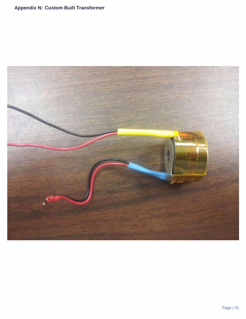
2.2.3 Transformer
This team originally intended to use an off the shelf transformer for stepping up the
output voltage from the H-bridge to be fed into the capacitor bank. Eventually it was necessary
to build our own transformer to suite the exact needs of this project. As this team lacked the
knowledge of transformer design, an advisor was contacted for the right design approach. The
transformer to be built was designed to step-up the 12V to 220V. The decision was made two
use a dual side plastic bobbin for the primary and secondary coils. Calculations done led us to
use using a metal ferrite core for a signal frequency of 20 kHz. The primary side turn numbers
were found to be 36 and 728 respectively.
2.2.4 Capacitor Bank
Detailed description of the design of Cockcroft multiplier exists in several locations
online. The circuit itself is extremely simple; the only task for this team was to determine the
appropriate number of stages and the type of diodes to use. A choice of .1uf electrolytic
capacitors and 1n4007 diodes were decided because of price, and availability. The number of
stages was determined from experimentation.
The table on the following page shows some of the testing done on the .1uf electrolytic
capacitors to determine the number of stages needed to hit the output voltage required for
airflow. Two separate tests were done, one with square wave fed from a function generator and
another, where the capacitor bank is driven directly from mains. The result show that 22 stages
will be needed in order to get to design voltage of 7.5kV with an input voltage of 120VAC. The
result of 22 stages with an input of 120VAC at 60Hz demonstrated to us that the initial voltage
through the capacitors must be high in order to lower the amount of stages that is needed. A
downside that was noticed during this testing was that the capacitors maximum voltage capacity
is only 450V which limited us in the amount of voltage gain we could have across each stage in
the ladder.

Page | 15
Figure 6: Voltage Output vs number of stages
2.2.5 Design and implement the Emitter and Collector System
The actual air ionization will be conducted through the emitters and collectors. The
emitters will be made out of 50µm tungsten wire that runs through the center of the channel.
Several emitters will be connected in series and in parallel across the length of the channel to
improve flow characteristics. The collector diodes will be made out of a fine metal mesh
connected to a common ground. This mesh will cover the cross section of each channel but
have a mesh size small enough to not impede airflow. The planned device will likely consist of
multiple channels of ionic coolers that are embedded within an aluminum heat sink.
It is known from theory that the ionization voltage of air is 33kV/cm. Since ionization
results in ozone creation, this value places a maximum voltage per distance that is usable inside
the project. Finding the exact distance between the emitter and collector units was done
experimentally, by creating a slider to allow us to test the airflow we received at different
distance values.
In order to be sure about the spacing needed between the emitter and collector wires, a
simple prototype device was conceived and produced. The prototype consists of two plastic
windows, a pair of emitter and collector wires, and the remains of an old CD/DVD drive. The
drive is disassembled and stripped of everything except for the sliding optical drive that was
used to read the CD/DVDs. One window is mounted perpendicular onto the structure of the
drive while the other window is mounted perpendicular onto the sliding component of the optical
drive on the drive. This provides for uniform and smooth distance changes between the two
windows. The wires are mounted horizontally; one on each window. The testing voltage circuit is
applied to the pair of wires with the distance between the two windows being the max. The
windows are slid closer together until either air flow or arcing between the wires is present. The
distance between the two wires that allows for the maximum air flow depends on the voltage
0
500
1000
1500
2000
2500
3000
3500
0 1 2 3 4 5 6 7 8 9 10
Output Voltage
Stages
120V Input

Page | 16
that is being applied. Through this method of experimentation it was found that the proper
distance between the emitter and collector was .25”
Figure 7: Slider unit for distance testing
Figure 8: Collector and emitter diagram
2.2.6 Case Design and Heat sink
The ionic cooler will be housed inside of an aluminum case. The case will need to be
designed so that the components are electrically isolated from the outside. The cooling grid and

Page | 17
heat sink will be packaged together. The individual units of the grid will cool along the channels
of the heat sink. The heat sink will be attached to an external heat source to mimic the cooling in
an electronic device.
2.2.7 Case – shape and fitting
The case is designed in such a way so that the entire structure, minus the lid, is held
together by two bolts. These bolts clamp the insulating pieces together around the heat sink,
providing sufficient safety from the internal components. The lid is held on by four sets of
magnets; each set consisting of two. A magnet is embedded in each corner on the inside of the
lid. The pair to each magnet is located on the inside of sidewalls of the enclosure, away from
any components that might be affected by the magnetic fields. The magnets apply more than
enough force to hold the simple lid into place.
Figure 9: Completed case assembly
2.2.8 Feedback control
In order to control the flow of the system it was necessary to create a feedback control
system to the Arduino. The method that was taken was to find the temperature of the heat sink
using a thermocouple unit. Thermocouple would return a voltage value that would be curve
fitted against temperature. From there the duty cycle of the PWM output to the high voltage
circuit could be adjusted based on the temperature
Page | 18
In order to minimize the complexity of this circuit, a standalone thermocouple amplifier
unit was found. The breakout board MAX1385 provided the entire amplifier unit and supporting
circuit structure for the thermocouple. The only thing that needed to be provided was the K-type
thermocouple that was necessary for the operation. This unit also had a expansive library
through the Arduino complier which made coding the unit extremely easy.
However, there was some difficulty seen with adjusting the duty cycle output. During
testing, lowering the duty cycle of the PWM output caused the transformer to act strangely. With
any duty cycle below 40% the transformer would start clicking, and the amperage draw would
increase. The reason for this could be that the lower duty cycle causes the transformer to
become saturated. A logical solution would have been to vary the voltage output of the PWM
wave rather than the frequency or duty cycle. Unfortunately the Ardiuno does not allow for
variable voltage output through its digital IO’s which made this method impossible.
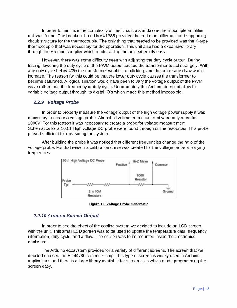
2.2.9 Voltage Probe
In order to properly measure the voltage output of the high voltage power supply it was
necessary to create a voltage probe. Almost all voltmeter encountered were only rated for
1000V. For this reason it was necessary to create a probe for voltage measurement.
Schematics for a 100:1 High voltage DC probe were found through online resources. This probe
proved sufficient for measuring the system.
After building the probe it was noticed that different frequencies change the ratio of the
voltage probe. For that reason a calibration curve was created for the voltage probe at varying
frequencies.
Figure 10: Voltage Probe Schematic
2.2.10 Arduino Screen Output
In order to see the effect of the cooling system we decided to include an LCD screen
with the unit. This small LCD screen was to be used to update the temperature data, frequency
information, duty cycle, and airflow. The screen was to be mounted inside the electronics
enclosure.
The Arduino ecosystem provides for a variety of different screens. The screen that we
decided on used the HD44780 controller chip. This type of screen is widely used in Arduino
applications and there is a large library available for screen calls which made programming the
screen easy.

Page | 19
2.3 Use
The intended purpose of the ionic cooling system detailed in this report is to cool
microelectronic devices. The device would work as a replacement or in conjunction with a rotary
fan. The benefits of this method of cooling over a rotary fan are that the ionic system can be
manufactured in a much smaller format. Power consumption is also less than a typical rotary
fan, although overall efficiency is lower. Since this type of cooling is intended for extremely small
low powered devices, the benefit of small size should outweigh the loss of efficiency.
The ultimate goal for this style of cooling is to manufacture ultra-small ionic cooling
system through micro fabrication. These small devices can then be embedded in the heat sinks
that attach to small IC’s in electronic devices. The benefit of this format is that it will allow for
forced convective cooling to be applied in situations where before only passive cooling has been
possible.

Page | 20
3 EVALUATION
3.1 Outcome
The outcome of this project is viewed in terms of the deliverables that this team
committed to and the function of the prototype unit. There were several project outcomes that
we wish to meet
1) Construction of the high voltage power supply
2) Construction of the emitter and collector units
3) Fabrication of the heat sink and collector units
4) Control the airflow through a feedback control system
5) Minimize the size of the unit as much as possible
This section will discuss these project goals in light of the
Table 1: Evaluation outcomes
Project Section Testing Method
Outcome
High voltage Power Supply Voltage Probe ~5kV measured
Emitter Collector Units Is there Airflow Yes, but only on some channels
Heat sink and Enclosure Fi t finish and Construction Rough, bad component placement
Feedback Control Controll ing Airflow Did not work
Miniaturization Qualitative Size As small as we could make i t

Page | 21
3.2 Testing and Results
3.2.1 The high Voltage circuit
The high voltage power supply circuit was measured by using the voltage probe at the
end of capacitor bank. Using the probe prompted .1cm long corona arcs when the probe was
placed near the electrode. When the probe was connected to the multimeter a measurement of
29V was seen. This would indicate a voltage of only ~5000kV which is far below the design
value that was needed.
The low voltage value can be attributed to the failure of the transformer to provide the
necessary voltage gain for the capacitor bank circuit. The transformer that we built only
measured 70VAC with an input voltage of 12VAC. This issue could be attributed to leakage
inductance caused by hand turning the transformer. This issue was attempted to be alleviated
by changing the frequency and duty cycle of the transformer. However, by trying to change
these values the transformers power consumption
Table 2: Power consumption and voltage consumption for transformer
Frequency (kHz) Voltage Current
25000 64.9 .164
20000 70.51 .130
15000 101.2 .1490
Duty Cycle %
50 70.51 .130
45 64.3 .178
40 58 .178
It was quickly discovered that changing the frequency and duty cycle of the PWM signal
proved insufficient in improving the performance of the transformer. Increasing the voltage fed
into the transformer was possible by using an external power source, but doing so would
eliminate the size constraint put on this project.
Location Voltage Measurement Device
Before Transformer 12V Multimeter
After Transformer 70.5V Multimeter
After Capacitor Bank ~5000V Voltage Probe
3.2.2 Power draw
The power draw of the unit was measured by connecting an antmeter up to the 12VDC
input of the system.
Table 3: Table of power consumption for the device
COMPONENT AMPERAGE (A) VOLTAGE POWER (W)

Page | 22
TOTAL .130 12 1.56
LCD SCREEN .160 5 .82
ARDUINO MEGA .10 5 .05W
The 1.56 W power usage usages is in conjunction with the ardiuno. The ardiuno itself
uses 10mA at 5V and the lcd screen pulls .82W of power. That means only approxmateily .70W
of power is going towards powering the actual ionic cooling unit. Other additional losses also
exist from the transformer and other parasitic losses, so the actual power consumption value
could be lower.
3.2.3 Emitter and Collector Units
Despite not getting the design value for voltage the emitter and collector units still
created some airflow across the unit. Measuring the air velocity of the flow proved difficult. We
used a qualitative measure of the airflow by using lighter and incense to see the flow movement
caused by the device. With this testing method, the device was able to blow out the flame of the
lighter at a distance of during testing, it was noticed that only two of the channels in the heat
sink were providing airflow.
3.2.4 Damage to the circuit
Unfortunately, during the testing of the unit we experienced a short somewhere in the
high voltage power supply. The short caused an arc from one of the capacitors to the screen of
the unit rendering both inoperable. The damage to the high voltage circuit was likely a blown
diode in the bootstrap circuit in the half-brdige driver. The screen was completely destroyed and
would need be replaced. Unfortunately, there was not enough time left to adequately fix these
components.

Page | 23
4 DISCUSSION
4.1 Assessment
In hindsight, this project ended up being far outside what this team expected. In the
original proposal of this project, it was thought that creating the electrical circuitry needed to
create the high voltage would be relatively easy. What ended up happening was several failed
circuits and a lot of resources and time being wasted on finding some type of circuit design that
did work. In reality none of the team had the electrical circuitry knowledge to build the unit, and
much of what was done in this capacity had to be learned while we progressed. Eventually, a
workable solution was found with the finalized circuit, but even then it did not work as intended.
The circuit shorted out during testing, likely because of insufficient insulation inside of the unit.
Had this project be chosen again, the team would immediately look to find an electrical
engineering student with proper knowledge in the area of ionic cooling. Far too much time was
spent on the electrical circuitry, when any EE student with basic knowledge could have
alleviated those issues.
In other areas there were problems. The enclosure unit was designed with a small
footprint in mind. However, it proved to be far too small for our needs. The screen and Ardiuno
mega barely fit inside the enclosure, and last second changes to the side panels had to be
made in order to get everything fitting properly inside the enclosure. The enclosure also wasn’t
designed with high voltage in mind. It was known by this group that the high voltage Cockcroft
Walton generator produced a high enough voltage to arc to metallic objects in its vicinity.
Despite this knowledge, no attempt was made at isolating this circuit from other components. In
the end, the capacitor bank ended up shorting to the LCD screen inside the enclosure which
destroyed the LCD screen and blew a diode (and also shocked a team member). A redesign of
this unit would have the electrical components far better isolated even if it resulted in a large
footprint.
Manufacturing also posed its own challenges. Originally the heat sink unit was to be
machined out of a single block of aluminum. This design was then changed into bolting together
fins cut out of sheet aluminum. The problem with this method was that in order to get the fin
geometry we wanted, the water jet unit had to be used. The water jet proved to be a hassle in
use due to inconsistency of the unit and the long down time that exist in between a single use.
Much time was wasted waiting for the water jet to operational, and resulted in a couple of parts
begin manufacturing far later than this team anticipated.
Dealing with the Arduino PWM output was also a problem. The original circuit that was
explored used two independent pwm outputs from the Arduino to drive a transformer. This
proved to be almost impossible in practice. The Arduino’s built in timers are extremely
rudimentary, and have it output two out of phase PWM waves was almost impossible without
using low level programming to interrupt the PWM in a cycle for the phase shift. It took almost
three weeks to find a workable solution, and the solution was as simple as adding a specialty
inverter chip after a single PWM output.
The transformer could also be improved. The transformer that was built was only
designed in the last week, when it was realized that other shelf bought transformers were not
Page | 24
going to work for out needs. The transformers that were attempted to use either were not rated
for the frequency range that we were using the circuit, or were so small that using them was
next to impossible. The one that was purposely built worked also did not work as intended. The
transformer was design for a 1:20 ratio, but in practice only produced 1:8. This was because of
the leakage inductance that is common in a hand wound transformer.
The results of the project were mixed. Of the original design goals that we set out to
achieve 3 of the 4 were completed. The only one thing that was unable to be accomplished was
direct feedback control of the high voltage circuitry.
During testing with the high frequency transformer and capacitor bank, it was discovered
that alternating the frequency to control the airflow as was originally described was not possible.
Large frequency changes up and down from the norm value of 20 kHz produced bad outcomes.
Lower frequencies caused the transformer to start crackling, and the amperage draw of the unit
to increase. High frequency did the same, so much so that in one test with 1Mhz frequency, the
transformer became so saturated that it back fed into the power supply we were using to test,
destroying the unit.
Another major issue was the inability to actually control the airflow of the unit. The
originally design incorporated frequency control of the output. This method proved impossible
with the type of transformer that was used. The only method that would work was to alter the
amplitude of the PWM wave from the Ardiuno. That circuit would easily be able to control the
output of the unit, but was not capable of being implanted in the timeframe that was available.
4.2 Next Steps
Although the project did not meet the all of the original design goals, the basic theory of
ionic cooling and its application towards microelectronics were shown. The device has no
moving parts, and extremely low power draw all of which make it attractive for use in those style
of devices. The small size of the device was created with just off the shelf components and
future work on miniaturization could create a device that is extremely small. Further work on the
high voltage circuit and transformer could lead to a unit that has a home in an electronic device.

Page | 25
5 CONCLUSION
The group’s approach towards a non-conventional thermal cooling method led to
research and development of an ionic cooling pump prototype that could eventually evolve into
a smaller cooling system that will be applicable to micro-electronics. The final assembly of the
ionic wind pump device included the manufactured hardware (heat sink) that was insulated from
the electronic components. It was shaped by the stable design of the heat sink, and furthermore
by the housing which also provided for further insulation.
Although successful tests were originally observed during the first stages of the
electronic component development, faulty measures taken during the final tests shorted the
circuitry and rendered the device inoperative upon assembly. It was due to the ever-changing
modifications needed for circuitry to satisfy the high voltage output required for device operation.
The device was designed not to short upon electrical arcing, but changes in circuitry during the
final stages of development left the assembly vulnerable towards malfunctioning because the
initial hardware set-up was not designed for the preceding electrical modifications. The short in
the system was due to faulty routing of the high-voltage emitter from the circuitry, where the
insulation proved to be too little for the final assembly.
Future attempts to complete a functional ionic wind pump would emphasize
modifications in hardware to complement any electrical changes from the original design. The
restrictive time, due to limited knowledge of overall circuitry, prevented major gains in the
group’s efforts through the method of trial and error. Each stage of development proved to be
an obstacle that was overcome, but draw backs and changes provided negative effects upon
completion of the finalized assembly. The device design and shorting of electrical components
prevents any further testing or modifications needed for a system to be present in working
condition.

Page | 26
REFERENCES
1) Tirumala, Rakshit. "CORONA DISCHARGES IN ASYMMETRIC ELECTRIC FIELDS AND ITS IMPACT
ON IONIC WIND GENERATION." Diss. University of Notre Dame, n.d. University of Notre Dame. Mar.
2013. Web. Apr. 2013. <http://www3.nd.edu/~sst/theses/2013_PhDThesis_Tirumala.pdf>.
2) N.E. Jewell-Larsen, E. Tran, I.A. Krichtafovitch, A.V. Mamishev, "Design and optimization of electrostatic fluid accelerators," IEEE Trans. Dielectr. Electr. 3) F. Yang, N.E. Jewell-Larsen, D.L. Brown, K. Pendergrass, D.A. Parker, I.A. Krichtafovitch, A.V. Mamishev, "Corona driven air propulsion for cooling of electronics," in XIII Int’l. Sympos. High Voltage Engineering (ISH),, Rotterdam, The Netherlands, 2003. 4) Chih-Peng Hsu; Jewell-Larsen, N.E.; Krichtafovitch, I.A.; Montgomery, S.W.; Dibene, J.T.; Mamishev, A.V., "Miniaturization of Electrostatic Fluid Accelerators," Microelectromechanical Systems, Journal of , vol.16, no.4, pp.809,815, Aug. 2007
5) Fritzius, Robert S. Ion Wind Generator. Rober S Fritzihus, assignee. Patent 3638058. 25 Jan. 1972.
Print.
6) Jewell-Larsen, N. E.; Ran, H.; Zhang, Y.; Schwiebert, M. K.; Tessera, K.A.H.; Mamishev, A.V.,
"Electrohydrodynamic (EHD) cooled laptop," Semiconductor Thermal Measurement and Management
Symposium, 2009. SEMI-THERM 2009. 25th Annual IEEE , vol., no., pp.261,266, 15-19 March 2009
7) J. F.W. Peek, Dielectric phenomenon in high voltage engineering, McGraw-HillBook Company, 1915.
8) J. Townsend, Electricity in gases, Oxford University Press, 1915.
9) M. Robinson, "Movement of air in the electric wind of the corona discharge," 10) Go, David B. ; Garimella , S V.; Fisher, Timothy; and Mongia, R. K., "Ionic Winds for Locally Enhanced Cooling" (2007). CTRC Research Publications. Paper 57. http://docs.lib.purdue.edu/coolingpubs/57 11) N.M. Brown, F.C. Lai, Electrohydrodynamic gas pump in a vertical tube, Journal of Electrostatics, Volume 67, Issue 4, July 2009, Pages 709-714, ISSN 0304-3886, 10.1016/j.elstat.2009.03.007. 12) International Rectifier. IR201 (S)(TR). DATA SHEET. N.p.: International Rectifier, 2004. Print.
PD60195-E.

Page | 27
A P P E N D I X

Page | 28
Appendix A: Drawing – Insulator

Page | 29
Appendix B: Drawing – Insulator End Fin
Page | 30
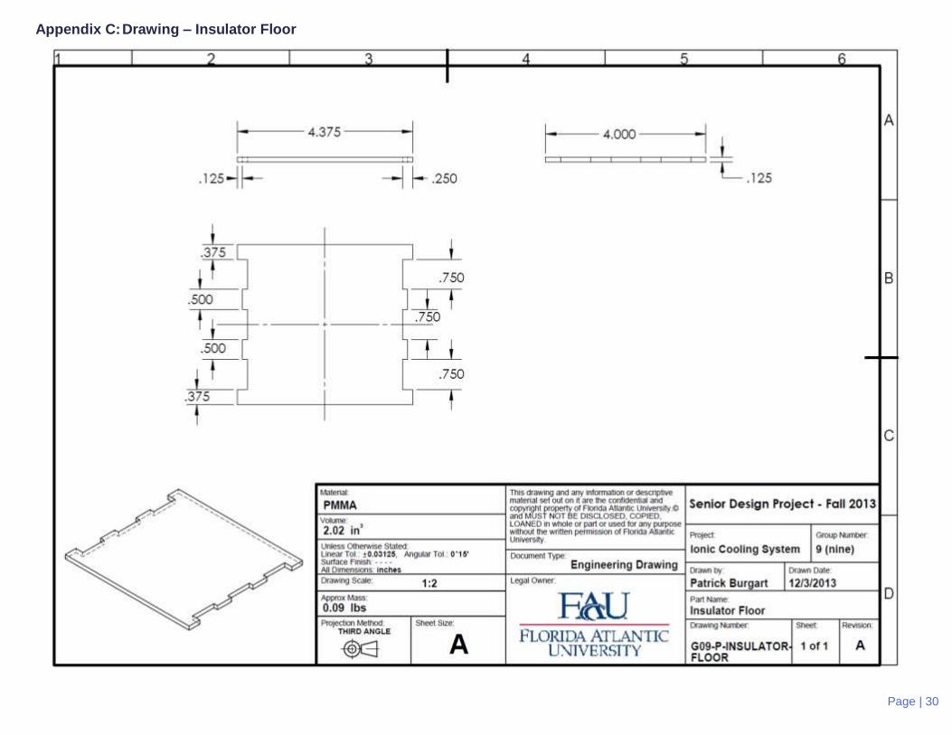
Appendix C: Drawing – Insulator Floor

Page | 31
Appendix D: Drawing – Insulator Side Wall – Display
Page | 32
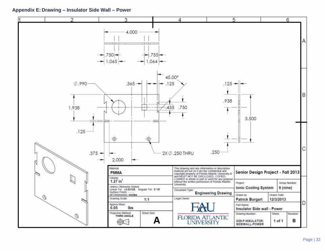
Appendix E: Drawing – Insulator Side Wall – Power
Page | 33
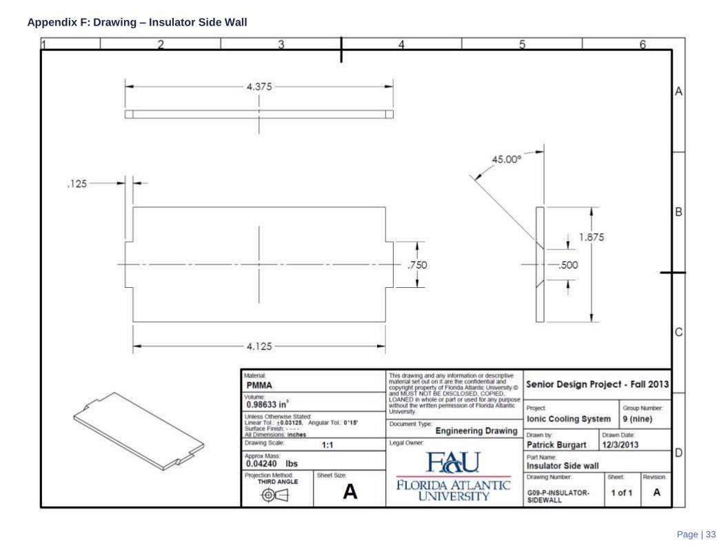
Appendix F: Drawing – Insulator Side Wall

Page | 34
Appendix G: Drawing – Lid

Page | 35
Appendix H: Drawing – Heat Sink Fin

Page | 36
Appendix I: Drawing – Heat Sink Spacer

Page | 37
Appendix J: Drawing – Assembly

Page | 38
Appendix K: Exploded assembly view

Page | 39
Appendix L: Probe testing data
Using Ground on transformer Output
20,000 HZ
69.69257656
V - Trans in V - Trans out V - Probe Multiplier
10 232.81 3.302 70.50575409
9 209.35 3.027 69.16088537
8 185.75 2.6871 69.12656768
7 161.92 2.347 68.99020026
6 138.51 1.967 70.4168785
5 114.82 1.63 70.44171779
4 91.5 1.302 70.2764977
3 68.25 0.984 69.3597561
2 45.08 0.6495 69.40723634
1 22.42 0.3238 69.24027177
60 Hz
211.0608495
V - Trans in V - Trans out V - Probe Multiplier
10 98.88 0.453 218.2781457
9 89.01 0.4081 218.1083068
8 78.83 0.3619 217.8226029
7 68.53 0.315 217.5555556
6 58.24 0.2681 217.232376
5 47.77 0.2204 216.7422868
4 37.42 0.174 215.0574713
3 27.225 0.1284 212.0327103
2 17.225 0.0845 203.8461538
1 7.7748 0.0447 173.9328859
10,000 Hz
95.63973318
V - Trans in V - Trans out V - Probe Multiplier
10 128.09 1.319 97.11144807
9 115.51 1.1892 97.13252607
8 102.75 1.0598 96.95225514
7 89.91 0.9284 96.84403274
6 76.09 0.7955 95.65053426
5 63.62 0.666 95.52552553
4 51.02 0.5359 95.20432917
3 38.25 0.403 94.91315136
2 25.435 0.2695 94.37847866
1 12.772 0.1378 92.6850508

Page | 40
Appendix M:Bill of Materials
Part Name Material Qty
Heat sink fin 6061 aluminum 11
Heat sink spacer 6061 aluminum 10
Insulator Polycarbonate 33
Insulator floor Polycarbonate 1
Insulator end fins Polycarbonate 2
Insulator wall - Short Polycarbonate 2
Insulator wall - Display Polycarbonate 1
Insulator wall - Power Polycarbonate 1
Lid Polycarbonate 1
Wire - Emitter Tungsten 2 feet
Wire - Collector Copper 2 feet
Bolt - hex 3/16 x 4-1/2 Zinc 2
Nut - Hex 3/16 Steel 2
Arduino Mega - - - 1
Wire - Jumper - - - 3
Wire - 16 AWG - - - 5 feet
Switch - Toggle - - - 1
Regulator - 5V - 7805 - - - 1
Socket - Wall wart - - - 1
Capacitor - 0.1 uf Electrolytic 24
Potentiometer - 10k - - - 1
Mosfet driver - IR2010 - - - 2
Mosfet - IRF630N - - - 4
Hex inverter - 7405 - - - 1
Resistor - 20 ohm - - - 4
Resistor - 10k ohm - - - 2
Diode - IN4148 Fast - - - 6
Diode - IN4007 - - - 24
Screen - 16x2 LCD HD47780 Liquid crystal 1
Circuit board - - - 2
Transformer - 20:1 high freq. - - - 1
Thermocouple - Controller - - - 1
Thermocouple - K-type - - - 1
Socket - 1 Pin - - - 8
Socket - 14 pin - - - 3
Bolt - M3 Nylon 8
Nut - M3 Nylon 8
Magnets - sphere Neodymium 8
Capacitor - 0.47 uf Ceramic 2
Capacitor - 47 uf Ceramic 2
Page | 41
Appendix N: Custom Built Transformer