laboratory 4 a: /2 b: /5 c: /8 tot: /15
TRANSCRIPT
EP-212 Electronics Lab-2 : Analog Electronics Page1/3
Name: Roll Number:___________________________________
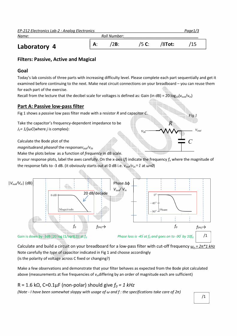
vin vout
C
R Fig 1
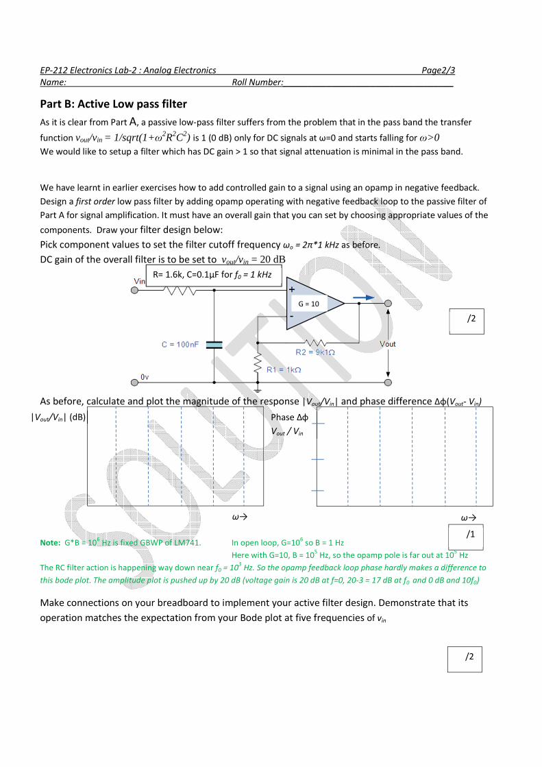
f(Hz)→
|Vout/Vin| (dB)
f(Hz)→
Phase Δφ
Vout/ Vin
/1
/1
Laboratory 4
Filters: Passive, Active and Magical
Goal
Today’s lab consists of three parts with increasing difficulty level. Please complete each part sequentially and get it
examined before continuing to the next. Make neat circuit connections on your breadboard – you can reuse them
for each part of the exercise.
Recall from the lecture that the decibel scale for voltages is defined as: Gain (in dB) = 20 log10(vout/vin)
Part A: Passive low-pass filter
Fig 1 shows a passive low pass filter made with a resistor R and capacitor C.
Take the capacitor’s frequency-dependent impedance to be
JC= 1/jωC(where j is complex):
Calculate the Bode plot of the
magnitudeand phaseof the responsevout/vin
Make the plots below as a function of frequency in dB scale.
In your response plots, label the axes carefully. On the x-axis (f) indicate the frequency fo where the magnitude of
the response falls to -3 dB. (it obviously starts out at 0 dB i.e. vout/vin=1 at ω=0)
Gain is down by -3dB [20 log (1/sqrt(2)] at f0 Phase loss is -45at f0 and goes on to -90
by 10f0
Calculate and build a circuit on your breadboard for a low-pass filter with cut-off frequency ωo = 2π*1 kHz
Note carefully the type of capacitor indicated in Fig 1 and choose accordingly
(is the polarity of voltage across C fixed or changing?)
Make a few observations and demonstrate that your filter behaves as expected from the Bode plot calculated
above (measurements at five frequencies of vindiffering by an order of magnitude each are sufficient)
R = 1.6 kΩ, C=0.1μF (non-polar) should give f0 = 1 kHz
(Note - I have been somewhat sloppy with usage of ω and f : the specifications take care of 2π)
A: /2B: /5 C: /8Tot: /15
20 dB/decade
f0 f0
EP-212 Electronics Lab-2 : Analog Electronics Page2/3
Name: Roll Number:___________________________________
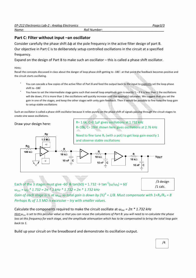
ω→
|Vout/Vin| (dB)
ω→
Phase Δφ
Vout / Vin
/2
/1
/2
G = 10
R= 1.6k, C=0.1μF for f0 = 1 kHz
Part B: Active Low pass filter
As it is clear from Part A, a passive low-pass filter suffers from the problem that in the pass band the transfer
function vout/vin = 1/sqrt(1+ω2R2C2) is 1 (0 dB) only for DC signals at ω=0 and starts falling for ω>0
We would like to setup a filter which has DC gain > 1 so that signal attenuation is minimal in the pass band.
We have learnt in earlier exercises how to add controlled gain to a signal using an opamp in negative feedback.
Design a first order low pass filter by adding opamp operating with negative feedback loop to the passive filter of
Part A for signal amplification. It must have an overall gain that you can set by choosing appropriate values of the
components. Draw your filter design below:
Pick component values to set the filter cutoff frequency ωo = 2π*1 kHz as before.
DC gain of the overall filter is to be set to vout/vin = 20 dB
As before, calculate and plot the magnitude of the response |Vout/Vin| and phase difference Δφ(Vout- Vin)
Note: G*B = 106 Hz is fixed GBWP of LM741. In open loop, G=10
6 so B = 1 Hz
Here with G=10, B = 105 Hz, so the opamp pole is far out at 10
5 Hz
The RC filter action is happening way down near f0 = 103 Hz. So the opamp feedback loop phase hardly makes a difference to
this bode plot. The amplitude plot is pushed up by 20 dB (voltage gain is 20 dB at f=0, 20-3 = 17 dB at f0 and 0 dB and 10f0)
Make connections on your breadboard to implement your active filter design. Demonstrate that its
operation matches the expectation from your Bode plot at five frequencies of vin
EP-212 Electronics Lab-2 : Analog Electronics Page3/3
Name: Roll Number:___________________________________
/3 design
/1 calc.
/4
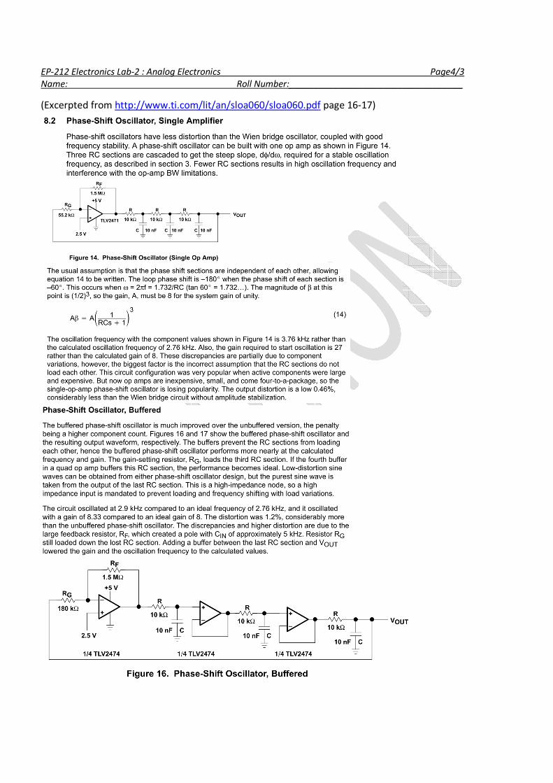
R= 1.6k, C=0.1μF gives oscillations at 1.732 kHz
R=10k, C= 10nF shown here gives oscillations at 2.76 kHz
Need to fine tune RF (with a pot) to get loop gain exactly 1
and observe stable oscillations
Part C: Filter without input –an oscillator
Consider carefully the phase shift Δφ at the pole frequency in the active filter design of part B.
Our objective in Part C is to deliberately setup controlled oscillations in the circuit at a specified
frequency.
Expand on the design of Part B to make such an oscillator – this is called a phase shift oscillator.
Hints:
Recall the concepts discussed in class about the danger of loop phase shift getting to -180: at that point the feedback becomes positive and
the circuit starts oscillating.
• You can cascade a few copies of the active filter of Part B and feed the output back to the input to explicitly set the loop phase
shift to -180
• You have to set the intermediate stage gains such that overall loop amplitude gain is exactly 1 – if it is less than 1 the oscillations
will die down, if it is more than 1 the oscillations will quickly increase until the opamp(s) saturates. We suggest that you set the
gain in one of the stages, and keep the other stages with unity gain feedback. Then it would be possible to fine-tune the loop gain
to setup stable oscillations
Such an oscillator is called a phase shift oscillator because it relies purely on the phase shift of signals passing through the circuit stages to
create sine wave oscillations.
Draw your design here:
Each of the 3 stages must give -60 & tan(60) = 1.732 → tan
-1(ω/ω0) = 60
ωosc = ω0 * 1.732 = 2π * 1 kHz * 1.732 = 2π * 1.732 kHz
Gain of each stage is ½ at ωosc so total gain is down by (½)3 = 1/8. Must compensate with 1+RF/RG = 8
Perhaps RF of 1.5 MΩ is excessive – try with smaller values.
Calculate the components required to make the circuit oscillate at ωosc = 2π * 1.732 kHz
Hint:ωosc is set to this peculiar value so that you can reuse the calculations of Part B: you will need to re-calculate the phase
loss at this frequency for each stage, and the amplitude attenuation which has to be compensated to bring the total loop gain
back to 1.
Build up your circuit on the breadboard and demonstrate its oscillation output.
+V
-V
EP-212 Electronics Lab-2 : Analog Electronics Page4/3
Name: Roll Number:___________________________________
(Excerpted from http://www.ti.com/lit/an/sloa060/sloa060.pdf page 16-17)