large area chemical vapour deposition grown transition
TRANSCRIPT

ARTICLE OPEN
Large area chemical vapour deposition grown transition metaldichalcogenide monolayers automatically characterizedthrough photoluminescence imagingToby Severs Millard1, Armando Genco 1✉, Evgeny M. Alexeev 1, Sam Randerson1, Seongjoon Ahn2, A-Rang Jang2,Hyeon Suk Shin2 and Alexander I. Tartakovskii 1✉
Chemical vapour deposition (CVD) growth is capable of producing multiple single-crystal islands of atomically thin transition metaldichalcogenides (TMDs) over large areas. Subsequent merging of perfectly epitaxial domains can lead to single-crystal monolayersheets, a step towards scalable production of high quality TMDs. For CVD growth to be effectively harnessed for such production itis necessary to be able to rapidly assess the quality of material across entire large area substrates. To date, characterisation has beenlimited to sub-0.1-mm2 areas, where the properties measured are not necessarily representative of an entire sample. Here, we applyphotoluminescence (PL) imaging and computer vision techniques to create an automated analysis for large area samples ofmonolayer TMDs, measuring the properties of island size, density of islands, relative PL intensity and homogeneity, and orientationof triangular domains. The analysis is applied to ×20 magnification optical microscopy images that completely map samples ofWSe2 on hBN, 5.0 mm × 5.0 mm in size, and MoSe2–WS2 on SiO2/Si, 11.2 mm × 5.8 mm in size. Two prevailing orientations ofepitaxial growth were observed in WSe2 grown on hBN and four predominant orientations were observed in MoSe2, initially grownon c-plane sapphire. The proposed analysis will greatly reduce the time needed to study freshly synthesised material over large areasubstrates and provide feedback to optimise growth conditions, advancing techniques to produce high quality TMD monolayersheets for commercial applications.
npj 2D Materials and Applications (2020) 4:12 ; https://doi.org/10.1038/s41699-020-0146-y
INTRODUCTIONVan der Waals layered crystals such as TMDs, hexagonal boronnitride (hBN) and graphene are defined by their strong covalentbonds in-plane and weak interlayer forces1. These characteristicsallow for individual atomically thin layers to be easily removedfrom the bulk crystal, and for single layers to be brought togetherto build vertical heterostructures that display promising newproperties1–3. As TMDs are exfoliated down to monolayerthickness their electronic band structure is altered due todimensional confinement, causing the materials to become directbandgap semiconductors that display photoluminescence (PL)under optical excitation4,5. MoSe2, WSe2, MoS2 and WS2 aredocumented as the most promising and widely studied TMDmonolayers, emitting bright PL while remaining stable in air, atroom temperature6. Such traits lend these materials to applica-tions in optoelectronic devices7 such as LEDs3,8, photovoltaiccells9,10, photodetectors11 and single photo-emitters12,13. Theiroptical properties have attracted further attention due to thepossibility for straightforward coupling to spin and valley degreesof freedom14. The extreme thinness and mechanical stability ofthese materials provide the potential for flexible and transparentdevices15. However, to realise such devices, the goal of scalableand controlled production of mono- and multilayers must first beachieved, an objective which has been of great interest forcommercial application ever since TMDs were rediscovered asatomically thin materials4,5.The original method of monolayer production, micromechanical
exfoliation2, produces high quality two-dimensional (2D) flakes,
but with a low yield and random nature it has an inherent inabilityto be scaled up. This has lead to a catalogue of methods beingdeveloped including other top-down approaches such as liquid-phase exfoliation16 and various forms of thinning17–19, as well asbottom-up routes such as wet-chemical synthesis20 and physicalvapour deposition21,22. A further technique, chemical vapourdeposition (CVD), has the capability to grow multiple monolayerislands across large area substrates and has been earmarked asthe process that will deliver scalable production23.Continuous lateral growth of these CVD islands leads to the in-
plane merging of single-crystal monolayers and eventually theformation of monolayer sheets. A problem encountered is that ifrandomly orientated, or irregularly shaped islands are allowed tocoalesce, grain boundaries are formed at every merger ofunaligned edges, which may negatively affect the optical andelectrical characteristics of the sheet24,25. The density of grainboundaries can be reduced through epitaxial growth of the TMDislands on substrates with hexagonal symmetry, such as hBN26–28,mica29, c-plane sapphire30,31 and graphene32. On these substrates,van der Waals interlayer interaction promotes the relativealignment despite the, often large, lattice mismatch33. In CVDthe morphology of islands can be controlled to a degree byaltering the local ratio of the transition metal and chalcogenatoms around a nucleation point. Typically the synthesised islandstake on a hexagonal or equilateral triangle shape34,35. The regularand reproducible triangular morphology is of particular interestwith respect to the production of continuous single-crystal films.On the majority of the crystalline substrates mentioned, hBN26–28,mica29 and graphene32, two well defined groups of triangular
1Department of Physics and Astronomy, University of Sheffield, Sheffield, UK. 2Department of Energy Engineering and Department of Chemistry, Ulsan National Institute ofScience and Technology (UNIST), Ulsan, South Korea. ✉email: [email protected]; [email protected]
www.nature.com/npj2dmaterials
Published in partnership with FCT NOVA with the support of E-MRS
1234567890():,;

islands rotated at 60° relative to one another are observed. Thesubsequent merging of these two groups results in either perfectstitching between objects at the same orientation, or theformation of mirror grain boundaries between those of opposite.On c-plane sapphire two more orientations were observed with amuch lower probability, both at a 30° rotation from the first set30.However, epitaxial growth is not a well-studied phenomenon
for any TMD and substrate combination, and it is generally onlyassessed manually across sub-0.1-mm2 areas, with analysiscontaining just hundreds of triangular crystals at most. Such smallsample sizes are not necessarily representative of the CVD growthacross an entire substrate, as all island properties, both physicaland optical, vary with spatial position. If this ordered growth canbe analysed across a larger area and a causality established withgrowth parameters, the gained feedback could be used forproduction of monolayer sheets with minimal grain boundaries,potentially realising commercial production of devices. Furtherrequirement for regular orientation of islands arises from potentialuses in van der Waals heterostructures, where a relative twistbetween adjacent layers is being actively researched as a newdegree of freedom36–42.Although the mechanisms that bring about the physical
properties of CVD grown material are believed to be understood20,to date, there are no documented methods to provide feedbackon an entire sample for optimisation of the desired propertiessuch as, island size and density, quality of PL emission andorientation of individual islands. If the quality of CVD grown TMDmonolayers is to improve and high-grade sheets and van derWaals heterostructures produced, it is first necessary to be able toreliably characterise entire large area samples.Computer vision has been used in the field of 2D materials,
predominantly as a tool for automatic mono- and multilayeridentification of exfoliated material across large areas43,44—freeing up time taken searching for flakes. The technique of PLimaging has been developed in parallel, as a fast and innovativetype of optical imaging, that can be simply applied to a standardoptical microscope for wide-field and fast capture of fluorescentmonolayer material45.
Here, these two techniques have been applied to create anautomated analysis capable of characterising substrates on whichCVD synthesis has been carried out. The size, orientation, relativeintensity and homogeneity of PL emission are analysed usingimage processing software for each TMD island on substrates upto 65mm2 in size, containing more than 100,000 individual islandsof one or two TMD materials. The analysis is demonstrated inapplication to two samples of WSe2 grown directly onto hBN(sample 1 and 2, both 5.0 mm × 5.0 mm) and a third sample(sample 3) containing MoSe2 and WS2 islands on SiO2/Si(11.2 mm × 5.8 mm), where the WS2 was grown directly ontothe substrate while the MoSe2 was grown on c-plane sapphireand subsequently transferred. The reported characterisation andanalysis can be extended to any combination of TMDs andsubstrate where PL is emitted at room temperature. For WSe2monolayers grown directly on hBN, we observe two equallypreferential orientations, while MoSe2 samples originally grown onc-plane sapphire and subsequently transferred onto SiO2/Sisubstrate demonstrate four prevalent preferential orientations.
RESULTSImaging and image processing frameworkWe use computer vision functions from the MATLAB imageprocessing toolbox46 to analyse the high-resolution PL image ofthe entire sample on a large substrate of a few 10 s of mm2,acquired by manually stitching the images taken with a ×20magnification microscope objective. The monolayer TMD islandswere identified through their PL as the only luminescent objectson the studied substrates, and their size and shape were extractedusing MATLAB shape recognition functions. Only monolayerislands with the shape close to equilateral triangle were used fororientation analysis, while monolayer islands with all morpholo-gies were used for size, mean PL intensity, and material coverageanalysis, as described below in this section, and further detailed inthe ‘Methods’ section and in Supplementary information.Figure 1a shows a schematic diagram of how a dichroic mirror
can be used to isolate PL emission in a generic microscope set-up,reflecting the visible light while transmitting in the near infrared45
Fig. 1 Imaging and image processing of CVD grown TMD monolayers. a A schematic showing how PL emission is isolated from thecollected light in a typical BF microscope set-up using a 550-nm short-pass filter, 550-nm long-pass dichoric mirror and 600-nm long-pass filtercombination. b–d A comparison between images at ×50 magnification obtained using BF (b), DF (c) and PL (d). In (d), the two materials areoutlined in light blue with MoSe2 appearing as a light pink colour and WS2 as a dark red. The image was taken with a 10 s exposure time and9.6x analogue gain. The red scale bars in each image are 50 μm. The binary image resulting from the image processing of (d) is shown in (e),with each individual object highlighted by their central point (centroid) shown by a blue marker, and their extrema shown by red dots.f Illustration of how the applied image analysis programme attempts to find a triangular outline of a single isolated island by combining ordiscarding the extrema, resulting in three clear combined points, E1-3. See further details in text and Supplementary Information(Supplementary Note 1). g A visual representation of how the programme calculates the orientation of each island from the positions of thecombined extrema, E1-3. The light blue equilateral triangle is fitted to each combinations of two points and the angle, θ, along with anuncertainty, is calculated.
T. Severs Millard et al.
2
npj 2D Materials and Applications (2020) 12 Published in partnership with FCT NOVA with the support of E-MRS
1234567890():,;
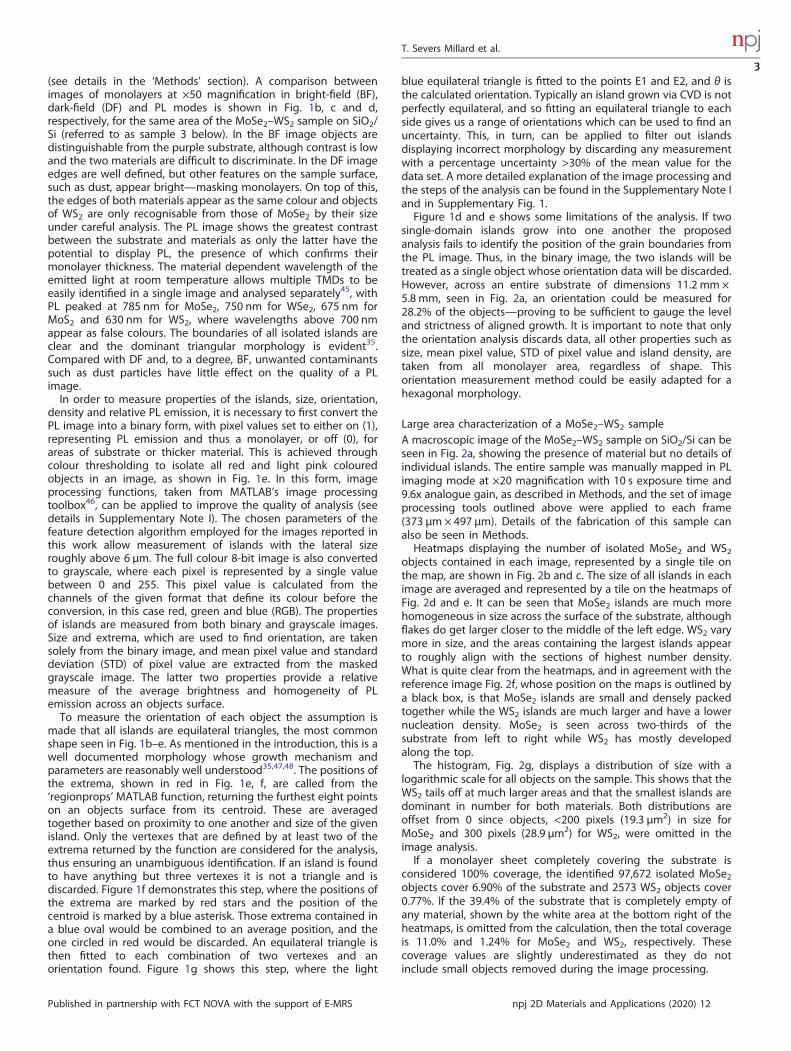
(see details in the ‘Methods’ section). A comparison betweenimages of monolayers at ×50 magnification in bright-field (BF),dark-field (DF) and PL modes is shown in Fig. 1b, c and d,respectively, for the same area of the MoSe2–WS2 sample on SiO2/Si (referred to as sample 3 below). In the BF image objects aredistinguishable from the purple substrate, although contrast is lowand the two materials are difficult to discriminate. In the DF imageedges are well defined, but other features on the sample surface,such as dust, appear bright—masking monolayers. On top of this,the edges of both materials appear as the same colour and objectsof WS2 are only recognisable from those of MoSe2 by their sizeunder careful analysis. The PL image shows the greatest contrastbetween the substrate and materials as only the latter have thepotential to display PL, the presence of which confirms theirmonolayer thickness. The material dependent wavelength of theemitted light at room temperature allows multiple TMDs to beeasily identified in a single image and analysed separately45, withPL peaked at 785 nm for MoSe2, 750 nm for WSe2, 675 nm forMoS2 and 630 nm for WS2, where wavelengths above 700 nmappear as false colours. The boundaries of all isolated islands areclear and the dominant triangular morphology is evident35.Compared with DF and, to a degree, BF, unwanted contaminantssuch as dust particles have little effect on the quality of a PLimage.In order to measure properties of the islands, size, orientation,
density and relative PL emission, it is necessary to first convert thePL image into a binary form, with pixel values set to either on (1),representing PL emission and thus a monolayer, or off (0), forareas of substrate or thicker material. This is achieved throughcolour thresholding to isolate all red and light pink colouredobjects in an image, as shown in Fig. 1e. In this form, imageprocessing functions, taken from MATLAB’s image processingtoolbox46, can be applied to improve the quality of analysis (seedetails in Supplementary Note I). The chosen parameters of thefeature detection algorithm employed for the images reported inthis work allow measurement of islands with the lateral sizeroughly above 6 μm. The full colour 8-bit image is also convertedto grayscale, where each pixel is represented by a single valuebetween 0 and 255. This pixel value is calculated from thechannels of the given format that define its colour before theconversion, in this case red, green and blue (RGB). The propertiesof islands are measured from both binary and grayscale images.Size and extrema, which are used to find orientation, are takensolely from the binary image, and mean pixel value and standarddeviation (STD) of pixel value are extracted from the maskedgrayscale image. The latter two properties provide a relativemeasure of the average brightness and homogeneity of PLemission across an objects surface.To measure the orientation of each object the assumption is
made that all islands are equilateral triangles, the most commonshape seen in Fig. 1b–e. As mentioned in the introduction, this is awell documented morphology whose growth mechanism andparameters are reasonably well understood35,47,48. The positions ofthe extrema, shown in red in Fig. 1e, f, are called from the‘regionprops’ MATLAB function, returning the furthest eight pointson an objects surface from its centroid. These are averagedtogether based on proximity to one another and size of the givenisland. Only the vertexes that are defined by at least two of theextrema returned by the function are considered for the analysis,thus ensuring an unambiguous identification. If an island is foundto have anything but three vertexes it is not a triangle and isdiscarded. Figure 1f demonstrates this step, where the positions ofthe extrema are marked by red stars and the position of thecentroid is marked by a blue asterisk. Those extrema contained ina blue oval would be combined to an average position, and theone circled in red would be discarded. An equilateral triangle isthen fitted to each combination of two vertexes and anorientation found. Figure 1g shows this step, where the light
blue equilateral triangle is fitted to the points E1 and E2, and θ isthe calculated orientation. Typically an island grown via CVD is notperfectly equilateral, and so fitting an equilateral triangle to eachside gives us a range of orientations which can be used to find anuncertainty. This, in turn, can be applied to filter out islandsdisplaying incorrect morphology by discarding any measurementwith a percentage uncertainty >30% of the mean value for thedata set. A more detailed explanation of the image processing andthe steps of the analysis can be found in the Supplementary Note Iand in Supplementary Fig. 1.Figure 1d and e shows some limitations of the analysis. If two
single-domain islands grow into one another the proposedanalysis fails to identify the position of the grain boundaries fromthe PL image. Thus, in the binary image, the two islands will betreated as a single object whose orientation data will be discarded.However, across an entire substrate of dimensions 11.2 mm ×5.8 mm, seen in Fig. 2a, an orientation could be measured for28.2% of the objects—proving to be sufficient to gauge the leveland strictness of aligned growth. It is important to note that onlythe orientation analysis discards data, all other properties such assize, mean pixel value, STD of pixel value and island density, aretaken from all monolayer area, regardless of shape. Thisorientation measurement method could be easily adapted for ahexagonal morphology.
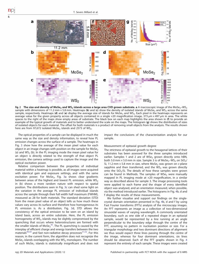
Large area characterization of a MoSe2–WS2 sampleA macroscopic image of the MoSe2–WS2 sample on SiO2/Si can beseen in Fig. 2a, showing the presence of material but no details ofindividual islands. The entire sample was manually mapped in PLimaging mode at ×20 magnification with 10 s exposure time and9.6x analogue gain, as described in Methods, and the set of imageprocessing tools outlined above were applied to each frame(373 μm× 497 μm). Details of the fabrication of this sample canalso be seen in Methods.Heatmaps displaying the number of isolated MoSe2 and WS2
objects contained in each image, represented by a single tile onthe map, are shown in Fig. 2b and c. The size of all islands in eachimage are averaged and represented by a tile on the heatmaps ofFig. 2d and e. It can be seen that MoSe2 islands are much morehomogeneous in size across the surface of the substrate, althoughflakes do get larger closer to the middle of the left edge. WS2 varymore in size, and the areas containing the largest islands appearto roughly align with the sections of highest number density.What is quite clear from the heatmaps, and in agreement with thereference image Fig. 2f, whose position on the maps is outlined bya black box, is that MoSe2 islands are small and densely packedtogether while the WS2 islands are much larger and have a lowernucleation density. MoSe2 is seen across two-thirds of thesubstrate from left to right while WS2 has mostly developedalong the top.The histogram, Fig. 2g, displays a distribution of size with a
logarithmic scale for all objects on the sample. This shows that theWS2 tails off at much larger areas and that the smallest islands aredominant in number for both materials. Both distributions areoffset from 0 since objects, <200 pixels (19.3 μm2) in size forMoSe2 and 300 pixels (28.9 μm2) for WS2, were omitted in theimage analysis.If a monolayer sheet completely covering the substrate is
considered 100% coverage, the identified 97,672 isolated MoSe2objects cover 6.90% of the substrate and 2573 WS2 objects cover0.77%. If the 39.4% of the substrate that is completely empty ofany material, shown by the white area at the bottom right of theheatmaps, is omitted from the calculation, then the total coverageis 11.0% and 1.24% for MoSe2 and WS2, respectively. Thesecoverage values are slightly underestimated as they do notinclude small objects removed during the image processing.
T. Severs Millard et al.
3
Published in partnership with FCT NOVA with the support of E-MRS npj 2D Materials and Applications (2020) 12
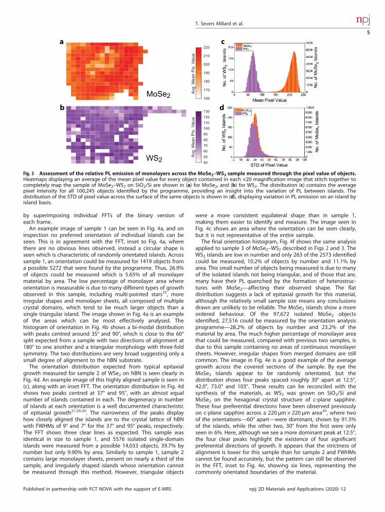
The optical properties of a sample can be displayed in much thesame way as the size and density information, to reveal how PLemission changes across the surface of a sample. The heatmaps inFig. 3 show how the average of the mean pixel value for eachobject in an image changes with position on the sample for MoSe2(a) and WS2 (b). In the PL imaging mode the mean pixel value foran object is directly related to the strength of that object PLemission, the camera settings used to capture the image and theoptical excitation power.Relative comparison between the properties of individual
material within a heatmap is possible, as all images were acquiredwith identical gain and exposure settings, and with the sameexcitation power. For MoSe2, Fig. 3a shows clear gradientsbetween areas of the highest and lowest PL emission, while WS2in (b) shows a more random nature with respect to spatialposition. The distributions seen in Fig. 3c can shed some light onthe variation in the average PL emission of individual islandsacross the sample through their full width half maximum (FWHM),measured as 28 for both materials. The standard deviation (STD)from the mean pixel value of an object tells us how much thesevalues vary across its surface and therefore how homogeneous itsPL emission is. As a distribution, Fig. 3d, STD allows theconsistency of the optical emission to be seen on an island byisland basis, across an entire substrate. Here, the PL emissionhomogeneity of WS2 islands may be slightly compromised by thequenching that occurs where heterostructures are formed withthe smaller islands of MoSe2
45. The PL quenching is caused by theinterplay of efficient charge and energy transfers between the twomaterials49,50 and fast non-radiative decay processes51,52. For thisreason, in the current form, the algorithm does not recognize theMoSe2 islands overlapping with the WS2 monolayers. The numberof such MoSe2 islands is statistically insignificant and does not
impact the conclusions of the characterization analysis for oursample.
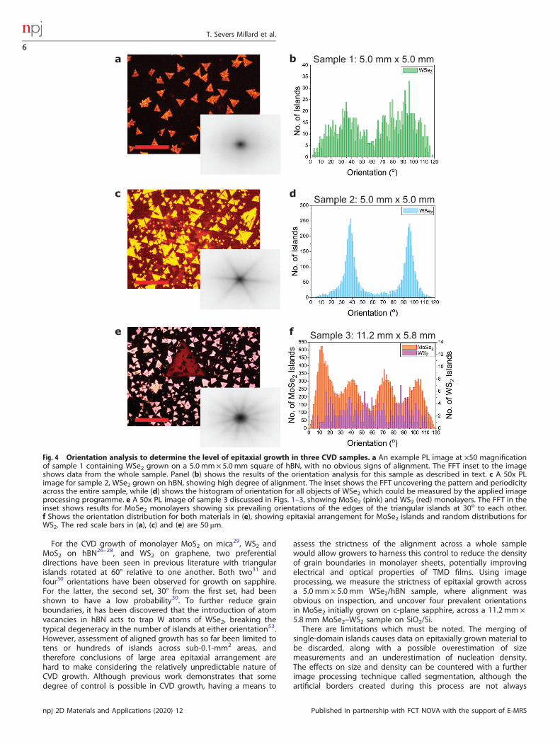
Measurement of epitaxial growth degreeThe strictness of epitaxial growth to the hexagonal lattices of theirsubstrates has been assessed for the three samples introducedearlier. Samples 1 and 2 are of WSe2 grown directly onto hBN,both 5.0 mm × 5.0 mm in size. Sample 3 is of MoSe2–WS2 on SiO2/Si, 11.2 mm × 5.8 mm in size, where MoSe2 was grown on c-planesapphire and then transferred, and the WS2 was grown directlyonto the SiO2/Si. The details of how these samples were growncan be found in Methods. The samples of WSe2 were manuallymapped in PL imaging mode at ×20 magnification, in a similarway as described above for sample 3. The image processing toolswere applied to each frame and the shape of every identifiedobject was analysed, and an orientation measured, when possible,via the method introduced earlier. The histograms in Fig. 4b, d andf display the results of these measurements.We further visualise and support our findings on the single-
crystal domain orientation presented in Fig. 4b, d and f by usingFast Fourier transforms (FFTs) analysis of the microscopy images.An FFT represents an image as a collection of two-dimensionalsinusoidal waves of varying wavelength. A commonly orientatedboundary, such as one side of a repeated shape in an epitaxialsample, would be represented by a line running at an angleperpendicular to the boundary edge through the centre of theFFT, assuming no pattern in nucleation position or size. For atriangular morphology and two dominant directions of alignmentwe thus would expect three lines passing through the centre ofthe image, whereas for four dominant orientations, six linesshould be observed. Each of the FFT graphs shown in Fig. 4represent the entirety of each sample. These images were created
Fig. 2 The size and density of MoSe2 and WS2 islands across a large area CVD grown substrate. a A macroscopic image of the MoSe2–WS2sample with dimensions of 11.2 mm× 5.8 mm. Heatmaps (b) and (c) show the density of isolated islands of MoSe2 and WS2 across the samesample, respectively. Heatmaps (d) and (e) display the average size of islands for MoSe2 and WS2. Each pixel in the heatmaps represents anaverage value for the given property across all objects contained in a single ×20 magnification image, 373 μm× 497 μm in area. The whitespaces to the right of the maps show empty areas of substrate. The black box on each map highlights the area shown in (f) to provide anexample of the typical growth of materials and to better understand the scale on the maps. The histogram (g) shows the distribution of sizesof isolated objects for each material. The offset for both materials is a product of removing small objects from the analysis. The results shownhere are from 97,672 isolated MoSe2 islands and 2573 of WS2.
T. Severs Millard et al.
4
npj 2D Materials and Applications (2020) 12 Published in partnership with FCT NOVA with the support of E-MRS
by superimposing individual FFTs of the binary version ofeach frame.An example image of sample 1 can be seen in Fig. 4a, and on
inspection no preferred orientation of individual islands can beseen. This is in agreement with the FFT, inset to Fig. 4a, wherethere are no obvious lines observed, instead a circular shape isseen which is characteristic of randomly orientated islands. Acrosssample 1, an orientation could be measured for 1419 objects froma possible 5272 that were found by the programme. Thus, 26.9%of objects could be measured which is 5.65% of all monolayermaterial by area. The low percentage of monolayer area whereorientation is measurable is due to many different types of growthobserved in this sample, including multi-pointed stars35, moreirregular shapes and monolayer sheets, all composed of multiplecrystal domains, which tend to be much larger objects than asingle triangular island. The image shown in Fig. 4a is an exampleof the areas which can be most effectively analysed. Thehistogram of orientation in Fig. 4b shows a bi-modal distributionwith peaks centred around 35° and 90°, which is close to the 60°split expected from a sample with two directions of alignment at180° to one another and a triangular morphology with three-foldsymmetry. The two distributions are very broad suggesting only asmall degree of alignment to the hBN substrate.The orientation distribution expected from typical epitaxial
growth measured for sample 2 of WSe2 on hBN is seen clearly inFig. 4d. An example image of this highly aligned sample is seen in(c), along with an inset FFT. The orientation distribution in Fig. 4dshows two peaks centred at 37° and 95°, with an almost equalnumber of islands contained in each. The degeneracy in numberof islands at each orientation is a well documented characteristicof epitaxial growth27,28,30. The narrowness of the peaks displayhow closely aligned the islands are to the crystal lattice of hBNwith FWHMs of 9° and 7° for the 37° and 95° peaks, respectively.The FFT shows three clear lines as expected. This sample wasidentical in size to sample 1, and 5576 isolated single-domainislands were measured from a possible 14,033 objects, 39.7% bynumber but only 9.90% by area. Similarly to sample 1, sample 2contains large monolayer sheets, present on nearly a third of thesample, and irregularly shaped islands whose orientation cannotbe measured through this method. However, triangular objects
were a more consistent equilateral shape than in sample 1,making them easier to identify and measure. The image seen inFig. 4c shows an area where the orientation can be seen clearly,but it is not representative of the entire sample.The final orientation histogram, Fig. 4f shows the same analysis
applied to sample 3 of MoSe2–WS2 described in Figs 2 and 3. TheWS2 islands are low in number and only 263 of the 2573 identifiedcould be measured, 10.2% of objects by number and 11.1% byarea. This small number of objects being measured is due to manyof the isolated islands not being triangular, and of those that are,many have their PL quenched by the formation of heterostruc-tures with MoSe2—affecting their observed shape. The flatdistribution suggests a lack of epitaxial growth for this material,although the relatively small sample size means any conclusionsdrawn are unlikely to be reliable. The MoSe2 islands show a moreordered behaviour. Of the 97,672 isolated MoSe2 objectsidentified, 27,516 could be measured by the orientation analysisprogramme—28.2% of objects by number and 23.2% of thematerial by area. The much higher percentage of monolayer areathat could be measured, compared with previous two samples, isdue to this sample containing no areas of continuous monolayersheets. However, irregular shapes from merged domains are stillcommon. The image in Fig. 4e is a good example of the averagegrowth across the covered sections of the sample. By eye theMoSe2 islands appear to be randomly orientated, but thedistribution shows four peaks spaced roughly 30° apart at 12.5°,42.0°, 73.0° and 103°. These results can be reconciled with thesynthesis of the materials, as WS2 was grown on SiO2/Si andMoSe2 on the hexagonal crystal structure of c-plane sapphire.These four preferential directions have been observed previouslyon c-plane sapphire across a 220 μm× 220 μm area30, where twoof the orientations—60° apart—were dominant, shown by 91.5%of the islands, while the other two, 30° from the first were onlyseen in 6%. Here, although we see a more dominant peak at 12.5°,the four clear peaks highlight the existence of four significantpreferential directions of growth. It appears that the strictness ofalignment is lower for this sample than for sample 2 and FWHMscannot be found accurately, but the pattern can still be observedin the FFT, inset to Fig. 4e, showing six lines, representing thecommonly orientated boundaries of the material.
a
b
MoSe2
WS2
c
d
Fig. 3 Assessment of the relative PL emission of monolayers across the MoSe2–WS2 sample measured through the pixel value of objects.Heatmaps displaying an average of the mean pixel value for every object contained in each ×20 magnification image that stitch together tocompletely map the sample of MoSe2–WS2 on SiO2/Si are shown in (a) for MoSe2, and (b) for WS2. The distribution (c) contains the averagepixel intensity for all 100,245 objects identified by the programme, providing an insight into the variation of PL between islands. Thedistribution of the STD of pixel value across the surface of the same objects is shown in (d), displaying variation in PL emission on an island byisland basis.
T. Severs Millard et al.
5
Published in partnership with FCT NOVA with the support of E-MRS npj 2D Materials and Applications (2020) 12
For the CVD growth of monolayer MoS2 on mica29, WS2 andMoS2 on hBN26–28, and WS2 on graphene, two preferentialdirections have been seen in previous literature with triangularislands rotated at 60° relative to one another. Both two31 andfour30 orientations have been observed for growth on sapphire.For the latter, the second set, 30° from the first set, had beenshown to have a low probability30. To further reduce grainboundaries, it has been discovered that the introduction of atomvacancies in hBN acts to trap W atoms of WSe2, breaking thetypical degeneracy in the number of islands at either orientation53.However, assessment of aligned growth has so far been limited totens or hundreds of islands across sub-0.1-mm2 areas, andtherefore conclusions of large area epitaxial arrangement arehard to make considering the relatively unpredictable nature ofCVD growth. Although previous work demonstrates that somedegree of control is possible in CVD growth, having a means to
assess the strictness of the alignment across a whole samplewould allow growers to harness this control to reduce the densityof grain boundaries in monolayer sheets, potentially improvingelectrical and optical properties of TMD films. Using imageprocessing, we measure the strictness of epitaxial growth acrossa 5.0 mm × 5.0 mm WSe2/hBN sample, where alignment wasobvious on inspection, and uncover four prevalent orientationsin MoSe2 initially grown on c-plane sapphire, across a 11.2 mm ×5.8 mm MoSe2–WS2 sample on SiO2/Si.There are limitations which must be noted. The merging of
single-domain islands causes data on epitaxially grown material tobe discarded, along with a possible overestimation of sizemeasurements and an underestimation of nucleation density.The effects on size and density can be countered with a furtherimage processing technique called segmentation, although theartificial borders created during this process are not always
Fig. 4 Orientation analysis to determine the level of epitaxial growth in three CVD samples. a An example PL image at ×50 magnificationof sample 1 containing WSe2 grown on a 5.0 mm× 5.0 mm square of hBN, with no obvious signs of alignment. The FFT inset to the imageshows data from the whole sample. Panel (b) shows the results of the orientation analysis for this sample as described in text. c A 50x PLimage for sample 2, WSe2 grown on hBN, showing high degree of alignment. The inset shows the FFT uncovering the pattern and periodicityacross the entire sample, while (d) shows the histogram of orientation for all objects of WSe2 which could be measured by the applied imageprocessing programme. e A 50x PL image of sample 3 discussed in Figs. 1–3, showing MoSe2 (pink) and WS2 (red) monolayers. The FFT in theinset shows results for MoSe2 monolayers showing six prevailing orientations of the edges of the triangular islands at 30o to each other.f Shows the orientation distribution for both materials in (e), showing epitaxial arrangement for MoSe2 islands and random distributions forWS2. The red scale bars in (a), (c) and (e) are 50 μm.
T. Severs Millard et al.
6
npj 2D Materials and Applications (2020) 12 Published in partnership with FCT NOVA with the support of E-MRS
accurate and it tends to overcompensate for the problem. On theother hand, for orientation, in most cases a large enough numberof objects can be detected across a substrate to give arepresentative measurement of the level of epitaxial growth.Any technique that relies on PL imaging will encounter similarproblems and a more complex method would be necessary toextract orientation and grain boundaries from merged domains.As can be seen in the Supplementary Fig. 2, the degree of epitaxialgrowth of objects can still be assessed in samples of 2D materialsthat do not emit PL at room temperature using DF imaging,providing the correct morphology is present.
DISCUSSIONA new automated analysis has been developed capable ofmeasuring the characteristics of monolayer islands across tensof mm2 areas of CVD grown TMD semiconductors, from imagesthat map the sample surface. The analysis uses PL imagingtechniques and can be applied to various combinations ofsemiconducting TMD monolayer and substrate which emit PL atroom temperature. Functions from MATLAB’s image processingtoolbox are used to measure island size and density, as well asrelative average value, and homogeneity of, PL emission.Importantly, for each isolated monolayer island across a samplewe measure orientation, and obtain data on the presence anddegree of epitaxial growth. An FFT analysis has been furtherapplied to uncover any underlying patterns in the sample and toverify the results of the orientation histogram. Four preferentialdirections of alignment, not apparent to the naked eye, werefound in MoSe2 islands grown on c-plane sapphire, a characteristicthat had not been seen previously to such a degree. This analysismethod coupled with the automated mapping of CVD samples inPL image mode forms a fast and reliable characterisation tool.With the use of dark-field imaging the analysis of epitaxial
growth can be extended to many other materials that do not emitPL. Such analysis will reduce the amount of time needed to studyCVD samples or 2D materials produced by other scalabletechniques, and has particular application to developing aconsistent method of production for high quality 2D monolayersheets and heterostructures. Applications in other thin filmmaterial systems, such as perovskite or organic semiconductorsare also possible.Image analysis will likely become the norm as progression in the
field leads to inevitable commercial production of devices thatrequire a consistent quality of TMD monolayer, without time forconstant manual inspection. The utility of the automated analysisdeveloped in this work comes in its ability to characterise thequality of grown material automatically and unearth patterns thatwould be missed by manual inspection, such as the fourpreferential directions found in material grown on c-planesapphire (Fig. 4f), and the quantitative level of homogeneity inMoSe2 island size across the same sample (Fig. 2d).With thousands of objects analysed, a statistical approach to
assessing the quality of an entire substrate can be taken, as well asthe ability to focus on the properties of individual islands such as,size, orientation and quality of PL emission. The analysis holds vastamounts of information, providing a deep understanding of thecharacteristics of a sample and the opportunity to quantitativelycompare samples grown under different conditions.
METHODSGrowth of single-layer WS2WS2 was grown on a SiO2 substrate via CVD. Before the growth of WS2,SiO2 was cleaned by a piranha solution and was spin-coated by sodiumcholate which acted as a seeding promoter. WO3 (99.998%, Alfa Aesar) wasdissolved in the water/ammonia solution (9:1) and 1mL of the solution wascoated on the crucible. This crucible was placed at the centre of the
furnace and 100mg of S (99.999%, Alfa Aesar) was placed at the upstreamentry of the furnace. Then, the temperature of the tube furnace wasincreased up to 900 °C for 24min under a steady flow of Ar gas (100 sccm)in the ambient condition. When the furnace reached 600 °C the Svaporised. Then, temperature of the tube furnace was maintained at 900 °Cfor 30min for the WS2 growth. Afterwards, the tube furnace was cooleddown to room temperature under the Ar flow.
Growth of single-layer MoSe2 and transfer to SiO2/SiMoSe2 was grown on c-plane sapphire by CVD. Two precursors, MoO3
(99.97%, Sigma-Aldrich) and Se (99.999%, Alfa Aesar), were used for thegrowth. One hundred and fifty milligrams of Se was placed at theupstream entry of the furnace and 60mg of MoO3 powder was placed atthe centre of the furnace. A crucible containing MoO3 was partially coveredby a SiO2/Si wafer to reduce intense evaporation of the precursor. Thesapphire substrate was located next to the crucible that contained MoO3.Before the tube furnace was heated, the tube was evacuated for 30minand filled with the Ar gas achieving ambient pressure. The temperature ofthe furnace was increased up to 600 °C for 18min under a steady flow of Argas (60 sccm) and H2 gas (12 sccm). When the furnace reached 600 °C, Sewas vaporised by heating the upstream entry of the tube up to 270 °Cusing a heating belt. Finally, temperature of the tube furnace wasincreased to 700 °C and maintained for 1 h for the MoSe2 growth.Afterwards, the tube furnace was cooled down to room temperature whilethe Ar flow was maintained without H2. To transfer MoSe2 on top of theSiO2/Si substrate containing WS2, polystyrene was used to maintain thesample quality instead of poly(methyl methacrylate) that has been widelyused previously54.
Growth of single-layer WSe2 on hBNTo fabricate WSe2 on hBN, multilayer hBN was initially grown on c-planesapphire55. WO3 (99.998%, Alfa Aesar) and Se (99.999%, Alfa Aesar), wereused for the WSe2 growth. Three hundred milligrams of Se was placed atthe upstream entry of the furnace and 120mg of WO3 powder was placedat the centre of the furnace. To reduce the influence of humidity, a smallamount of NaCl was mixed with WO3 powder. The multilayer hBN onsapphire substrate was positioned next to the crucible containing WO3.Before the tube furnace was heated, the tube was evacuated for more than30min. Then, the temperature of the tube furnace was increased to 800 °Cfor 24min under a steady flow of Ar gas (120 sccm) and H2 gas (20 sccm).When the furnace reached 800 °C, the Se was vaporised by heating theupstream entry of the tube to 270 °C using a heating belt. Finally,temperature of the tube furnace was increased to 870 °C and maintainedfor 1 h for the WSe2 growth. Afterwards, the tube furnace was cooled downto room temperature under Ar flow.
PL imagingThe PL images analysed, such as Fig. 1d, were taken with an adaptedindustrial microscope (LV150N, Nikon). A 550-nm short-pass filter ispositioned in the path of the white light from the illumination source and a600-nm long-pass filter is placed before the camera (DS-Vi1, Nikon) toisolate PL emission. A further 550 long-pass dichroic mirror is applied todirect the excitation light and collected PL emission. A detailed descriptionof the method can be found in ref. 45. Using this technique, the samplesdiscussed in reference to Fig. 1 through 4 were mapped manually at ×20magnification. The images of WSe2 on hBN were taken with 4 s exposuretime and an analogue gain of 5.6x, those of MoSe2–WS2 on SiO2/Si weretaken with 10 s and 9.6x, respectively. Each image was 373 μm× 497 μmin area.
Image processingImages were analysed in MATLAB using functions from the imageprocessing toolbox46. The colour thresholding application was used toisolate monolayer material in a PL image and was applied to eachcombination of monolayer and substrate. The ‘regionprops’ function wasused for the analysis of size, island density and pixel value with minimalcustom code. The programme that measured the orientation of equilateraltriangles was developed specifically for the analysis of epitaxial growth. Ittook the programme 43 s to analyse the orientation of the images forsample 1 containing 5272 objects, 69 s to analyse that of sample 2 of14,033 objects, and 1 h 8min and 13 s to analyse sample 3 containing100,245 objects of two different colours. FFTs, representing entire
T. Severs Millard et al.
7
Published in partnership with FCT NOVA with the support of E-MRS npj 2D Materials and Applications (2020) 12

substrates, were created by superimposing individual image FFTs and weresubsequently artificially enhanced for clarity by transforming the pixelvalues using contrast-limited adaptive histogram equalisation. Furtherdetails of the image processing and a more complete explanation of theanalysis can be found in the Supplementary Note I.
DATA AVAILABILITYThe data that support the findings of this study are available from the correspondingauthor upon reasonable request.
CODE AVAILABILITYThe codes that support the findings of this study are available from thecorresponding author upon reasonable request.
Received: 23 December 2019; Accepted: 10 April 2020;
REFERENCES1. Geim, A. K. & Grigorieva, I. V. Van der Waals heterostructures. Nature 499, 419
(2013).2. Novoselov, K. S. et al. Two-dimensional atomic crystals. Proc. Natl Acad. Sci. USA
102, 10451–10453 (2005).3. Withers, F. et al. Light-emitting diodes by band-structure engineering in van der
Waals heterostructures. Nature Mater. 14, 301 (2015).4. Mak, K. F., Lee, C., Hone, J., Shan, J. & Heinz, T. F. Atomically thin MoS2: a new
direct-gap semiconductor. Phys. Rev. Lett. 105, 136805 (2010).5. Splendiani, A. et al. Emerging photoluminescence in monolayer MoS2. Nano Lett.
10, 1271–1275 (2010).6. Tonndorf, P. et al. Photoluminescence emission and Raman response of mono-
layer MoS2, MoSe2, and WSe2. Opt. Express 21, 4908–4916 (2013).7. Pospischil, A. & Mueller, T. Optoelectronic devices based on atomically thin
transition metal dichalcogenides. Appl. Sci. 6, 78 (2016).8. Ross, J. S. et al. Electrically tunable excitonic light-emitting diodes based on
monolayer WSe2 p–n junctions. Nat. Nanotechnol. 9, 268 (2014).9. Pospischil, A., Furchi, M. M. & Mueller, T. Solar-energy conversion and light
emission in an atomic monolayer p–n diode. Nature Nanotechnol. 9, 257 (2014).10. Wu, K., Ma, H., Gao, Y., Hu, W. & Yang, J. Highly-efficient heterojunction solar cells
based on two-dimensional tellurene and transition metal dichalcogenides. J.Mater. Chem. A 7, 7430–7436 (2019).
11. Huo, N. & Konstantatos, G. Recent progress and future prospects of 2D-basedphotodetectors. Advanced Materials 30, 1801164 (2018).
12. Koperski, M. et al. Single photon emitters in exfoliated WSe2 structures. NatureNanotechnol. 10, 503 (2015).
13. Palacios-Berraquero, C. Quantum Confined Excitons in 2-Dimensional Materials71–89 (Springer, 2018).
14. Schaibley, J. R. et al. Valleytronics in 2D materials. Nat. Rev. Mater. 1, 16055 (2016).15. Akinwande, D., Petrone, N. & Hone, J. Two-dimensional flexible nanoelectronics.
Nat. Commun. 5, 5678 (2014).16. Backes, C. et al. Guidelines for exfoliation, characterization and processing of
layered materials produced by liquid exfoliation. Chem. Mater. 29, 243–255(2016).
17. Castellanos-Gomez, A. et al. Laser-thinning of MoS2: on demand generation of asingle-layer semiconductor. Nano Lett. 12, 3187–3192 (2012).
18. Varghese, A., Sharma, C. H. & Thalakulam, M. Topography preserved microwaveplasma etching for top-down layer engineering in MoS2 and other van der Waalsmaterials. Nanoscale 9, 3818–3825 (2017).
19. Huang, Y. et al. An innovative way of etching MoS2: characterization andmechanistic investigation. Nano Res. 6, 200–207 (2013).
20. Samadi, M. et al. Group 6 transition metal dichalcogenide nanomaterials:synthesis, applications and future perspectives. Nanoscale Horiz. 3, 90–204 (2018).
21. Wasa, K.; Kanno, I. & Kotera, H. Handbook of Sputter Deposition Technology:Fundamentals and Applications for Functional Thin Films, Nano-materials andMEMS (William Andrew, 2012).
22. Muratore, C. et al. Continuous ultra-thin MoS2 films grown by low-temperaturephysical vapor deposition. Appl. Phys. Lett. 104, 261604 (2014).
23. Shi, Y., Li, H. & Li, L.-J. Recent advances in controlled synthesis of two-dimensionaltransition metal dichalcogenides via vapour deposition techniques. Chem. Soc.Rev. 44, 2744–2756 (2015).
24. Najmaei, S. et al. Electrical transport properties of polycrystalline monolayermolybdenum disulfide. ACS Nano 8, 7930–7937 (2014).
25. Ly, T. H. et al. Misorientation-angle-dependent electrical transport acrossmolybdenum disulfide grain boundaries. Nat. Commun. 7, 10426 (2016).
26. Okada, M. et al. Direct chemical vapor deposition growth of WS2 atomic layers onhexagonal boron nitride. ACS Nano 8, 8273–8277 (2014).
27. Yan, A. et al. Direct growth of single-and few-layer MoS2 on h-BN with preferredrelative rotation angles. Nano Lett. 15, 6324–6331 (2015).
28. Yu, H. et al. Precisely aligned monolayer MoS2 epitaxially grown on h-BN basalplane. Small 13, 1603005 (2017).
29. Ji, Q. et al. Epitaxial monolayer MoS2 on mica with novel photoluminescence.Nano Lett. 13, 3870–3877 (2013).
30. Dumcenco, D. et al. Large-area epitaxial monolayer MoS2. ACS Nano 9, 4611–4620(2015).
31. Zhang, X. et al. Diffusion-controlled epitaxy of large area coalesced WSe2monolayers on sapphire. Nano Lett. 18, 1049–1056 (2018).
32. Bianco, G. et al. Direct epitaxial CVD synthesis of tungsten disulfide on epitaxialand CVD graphene. RSC Adv. 5, 98700–98708 (2015).
33. Nakanishi, T. et al. The atomic and electronic structure of 0∘ and 60∘ grainboundaries in MoS2. Front. Phys. 7, 59 (2019).
34. Yang, S. Y., Shim, G. W., Seo, S.-B. & Choi, S.-Y. Effective shape-controlled growthof monolayer MoS2 flakes by powder-based chemical vapor deposition. Nano Res.10, 255–262 (2017).
35. Wang, S. et al. Shape evolution of monolayer MoS2 crystals grown by chemicalvapor deposition. Chem. Mater. 26, 6371–6379 (2014).
36. Van Der Zande, A. M. et al. Tailoring the electronic structure in bilayer molyb-denum disulfide via interlayer twist. Nano Lett. 14, 3869–3875 (2014).
37. Liu, K. et al. Evolution of interlayer coupling in twisted molybdenum disulfidebilayers. Nat. Commun. 5, 4966 (2014).
38. Kunstmann, J. et al. Momentum-space indirect interlayer excitons in transition-metal dichalcogenide van der Waals heterostructures. Nat. Phys. 14, 801–805(2018).
39. Alexeev, E. M. et al. Resonantly hybridized excitons in moiré superlattices in vander Waals heterostructures. Nature 567, 81 (2019).
40. Jin, C. et al. Observation of moiré excitons in WSe2/WS2 heterostructure super-lattices. Nature 567, 76–81 (2019).
41. Seyler, K. L. et al. Signatures of moiré-trapped valley excitons in MoSe2/WSe2heterobilayers. Nature 567, 66–70 (2019).
42. Tran, K. et al. Evidence for moiré excitons in van der Waals heterostructures.Nature 567, 71–75 (2019).
43. Jessen, B. S. et al. Quantitative optical mapping of two-dimensional materials. Sci.Rep. 8, 6381 (2018).
44. Lee, J. et al. Highly efficient computer algorithm for identifying layer thicknessof atomically thin 2D materials. J. Phys. D App. Phys. 51, 11LT03 (2018).
45. Alexeev, E. M. et al. Imaging of interlayer coupling in van der Waals hetero-structures using a bright-field optical microscope. Nano Lett. 17, 5342–5349(2017).
46. MathWorks. Image Processing Toolbox User’s Guide 195–207 (MathWorks,2017).
47. Govind Rajan, A., Warner, J. H., Blankschtein, D. & Strano, M. S. Generalizedmechanistic model for the chemical vapor deposition of 2D transition metaldichalcogenide monolayers. ACS Nano 10, 4330–4344 (2016).
48. You, J., Hossain, M. D. & Luo, Z. Synthesis of 2D transition metal dichalcogenidesby chemical vapor deposition with controlled layer number and morphology.Nano Converg. 5, 26 (2018).
49. Kozawa, D. et al. Evidence for fast interlayer energy transfer in MoSe2/WS2 het-erostructures. Nano Lett. 16, 4087–4093 (2016).
50. Ceballos, F., Bellus, M., Chiu, H. & Zhao, H. Probing charge transfer excitons in aMoSe2-WS2 van der Waals heterostructure. Nanoscale 7, 17523–17528 (2015).
51. Ovesen, S. et al. Interlayer exciton dynamics in van der Waals heterostructures.Commun. Phys. 2, 1–8 (2019).
52. Selig, M. et al. Dark and bright exciton formation, thermalization, and photo-luminescence in monolayer transition metal dichalcogenides. 2D Mater. 5,035017 (2018).
53. Zhang, X. et al. Defect-controlled nucleation and orientation of WSe2 onhBN: a route to single-crystal epitaxial monolayers. ACS Nano 13, 3341–3352(2019).
54. Gurarslan, A. et al. Surface-energy-assisted perfect transfer of centimeter-scalemonolayer and few-layer MoS2 films onto arbitrary substrates. ACS Nano 8,11522–11528 (2014).
55. Jang, A.-R. et al. Wafer-scale and wrinkle-free epitaxial growth of single-orientated multilayer hexagonal boron nitride on sapphire. Nano Lett. 16,3360–3366 (2016).
T. Severs Millard et al.
8
npj 2D Materials and Applications (2020) 12 Published in partnership with FCT NOVA with the support of E-MRS

ACKNOWLEDGEMENTST.S.M., A.G., E.M.A. and A.I.T. acknowledge funding by EPSRC (EP/P026850/1). S.R. andA.I.T. acknowledge support from the SURE scheme of the University of Sheffield. Thiswork was supported by the research fund (NRF-2017R1E1A1A01074493) by theMinistry of Science and ICT, Korea. E.M.A. and A.I.T. thank the financial support of theGraphene Flagship under grant agreements 785219.
AUTHOR CONTRIBUTIONSThe samples were grown by S.A., A.J. and H.S.S. S.R. manually mapped the sample ofMoSe2–WS2 and T.S.M. mapped those of WSe2. T.S.M., A.G. and E.M.A. developed theMATLAB script for the computer analysis. T.S.M. analysed all images and produceddata for the paper. T.S.M., A.G. and A.I.T. wrote the paper with contributions from allco-authors. A.I.T. conceived and supervised the project.
COMPETING INTERESTSThe authors declare no competing interests.
ADDITIONAL INFORMATIONSupplementary information is available for this paper at https://doi.org/10.1038/s41699-020-0146-y.
Correspondence and requests for materials should be addressed to A.G. or A.I.T.
Reprints and permission information is available at http://www.nature.com/reprints
Publisher’s note Springer Nature remains neutral with regard to jurisdictional claimsin published maps and institutional affiliations.
Open Access This article is licensed under a Creative CommonsAttribution 4.0 International License, which permits use, sharing,
adaptation, distribution and reproduction in anymedium or format, as long as you giveappropriate credit to the original author(s) and the source, provide a link to the CreativeCommons license, and indicate if changes were made. The images or other third partymaterial in this article are included in the article’s Creative Commons license, unlessindicated otherwise in a credit line to the material. If material is not included in thearticle’s Creative Commons license and your intended use is not permitted by statutoryregulation or exceeds the permitted use, you will need to obtain permission directlyfrom the copyright holder. To view a copy of this license, visit http://creativecommons.org/licenses/by/4.0/.
© The Author(s) 2020
T. Severs Millard et al.
9
Published in partnership with FCT NOVA with the support of E-MRS npj 2D Materials and Applications (2020) 12