lic student copy
DESCRIPTION
LIC Lab ManualTRANSCRIPT

EC6412: Linear Integrated Circuits Lab Department of ECE 2014 - 2015
INDEX
Name of the student: Department:
Roll no.: Reg. No.:
Lab-in-charges:
S.No. Date Name of the ExperimentPage No
Date of Sub
MarksStaff Sign
Date
St. Joseph’s College of Engineering / 1 ISO 9001:2008St. Joseph’s Institute of Technology

EC6412: Linear Integrated Circuits Lab Department of ECE 2014 - 2015
University Syllabus:EC6412-LINEAR INTEGRATED CIRCUITS LAB L T P C 0 0 3 2
Design and Testing of:1. Inverting, Non inverting and differential amplifiers2. Integrator and Differentiator3. Instrumentation amplifier4. Active low-pass, High-pass and band-pass filters5. Astable & Monostable multivibrators and Schmitt Trigger using op-amp6. Phase shift and Wien bridge oscillators using op-amp7. Astable and monostable multivibrators using NE555 Timer8. PLL characteristics and its use as Frequency Multiplier9. DC power supply using LM317 and LM72310. Study of SMPS
Simulation Using SPICE:1. Simulation of Experiments 3, 4, 5, 6 and 72. D/A and A/D converters (Successive approximation)3. Analog multiplier4. CMOS Inverter, NAND and NOR
LIST OF EXPERIMENTSDesign& Testing of:1. Inverting, Non Inverting And Differential Amplifier2. Integrator And Differentiator3. Instrumentation Amplifier4. Second Order Active Filters5. Band Pass Filter6. Astable Multivibrator Using Op-Amp IC 7417. Monostable Multivibrator Using Op-Amp IC 7418. Schmitt Trigger (Regenerative Comparator)9. RC Phase Shift Oscillator10. Wien Bridge Oscillator11. Design Of Astable Multivibrator Using IC 555 Timer12. Design Of Monostable Multivibrator Using IC 555 Timer13. PLL (IC 565) characteristics and its use as Frequency Multiplier14. IC Regulated DC Power Supply Using LM723 And LM317
Study Of:15. SMPS
SIMULATION EXPERIMENTS USING PSPICE1. Instrumentation Amplifier 2. Second Order Active Filters 3. Active Band Pass Filters4. Astable Multivibrator (Using Op-amp and IC 555 Timer)5. Schmitt Trigger (Regenerative Comparator)6. Monostable Multivibrator (Using Op-amp and IC 555 Timer)7. RC Phase Shift Oscillator 8. Wien Bridge Oscillator 9. a) Digital to Analog Convertor.
b) Analog to Digital Converter. 10. Analog Multiplier 11. CMOS IC’s Invertor, NAND and NOR gate.
St. Joseph’s College of Engineering / 2 ISO 9001:2008St. Joseph’s Institute of Technology

EC6412: Linear Integrated Circuits Lab Department of ECE 2014 - 2015
Ex. No:1 INVERTING, NON-INVERTING AND DIFFERENTIAL AMPLIFIER
Date:
AIM:To design, construct and test inverting, non-inverting and differential amplifier using IC 741.APPARATUS REQUIRED:
S.No. Name of the Apparatus Range/Value Qty
1. Bread Board - 1
2. RPS (0-30) V 2
3. Dual Power Supply ±15 V 1
4. Resistor 1k Ω,10k Ω 2,2
5. IC 741 Op-Amp - 1
6. Connecting Wires - Few
7. Function Generator (0-3) MHz 1
8. CRO (0-30) MHz 1
9. Voltmeter or Multi-meter (0-30) V 1
DESIGN:INVERTING AMPLIFIER: To design an amplifier for the gain of -10.Gain = Rf/R1.As the Gain is given negative, the circuit is inverting amplifier.Gain Av = Rf/R1 = 10 => Rf= 10 R1. Let R1= 1k, Rf = 10 * R1 = 10 * 1k = 10k.NON - INVERTING AMPLIFIER: To design an amplifier for the gain of 11.Gain = 1+ Rf/R1.As the Gain is given positive, the circuit is non-inverting amplifier.Gain Av = 1+Rf/R1 = 11 => Rf = 10 R1. Let R1= 1k, Rf = 10 * R1 = 10 * 1k = 10k.THEORY:INVERTING AMPLIFIER: A typical inverting amplifier with input resistor R1and a feedback resistor Rf is shown in the figure. Since the op-amp is assumed to be an ideal one the input bias current is zero and hence the non -inverting input terminal is at ground potential. The voltage at node ‘A’ is Zero, as the non inverting input terminal is grounded. The nodal equation by KCL at node ‘A’ is given by Vi/R1 + Vo/Rf =0 or V0 = -Rf (Vi/R1).NON- INVERTING AMPLIFIER: A typical noninverting amplifier with input resistor R1 and a feedback resistor Rf is shown in the figure. The input voltage is given to the positive terminal. The output voltage is given by V0= (1+Rf /R1) ViDIFFERENTIAL AMPLIFIER: Basic differential amplifier is shown in figure, it amplifies the difference between the two input signal applied. The differential amplifier is characterized by the common mode rejection ratio (CMRR), which is the ratio of differential gain to common mode gain. The output voltage is given by V0 = (R2 / R1) (V1 – V2), where V1 and V2 are the input voltages.CIRCUIT DIAGRAM:INVERTING AMPLIFIER TABULATION:
St. Joseph’s College of Engineering / 3 ISO 9001:2008St. Joseph’s Institute of Technology
Wave-form
Time Period in ms
Voltage in Volts
Practical Gain
Input
(Vin)
Output
(Vo)

EC6412: Linear Integrated Circuits Lab Department of ECE 2014 - 2015
NON INVERTING AMPLIFIER
DIFFERENTIAL AMPLIFIER
PROCEDURE:(i) Connect the inverting amplifier circuit as per the circuit diagram.(ii) For various input voltage measure and record the output voltage.(iii) Repeat the same for non- inverting and differential amplifier.MODEL GRAPH:INVERTING AMPLIFIER NON-INVERTING AMPLIFIER
St. Joseph’s College of Engineering / 4 ISO 9001:2008St. Joseph’s Institute of Technology
Wave-
form
Time
in ms
Voltage
in Volts
Practical
Gain
Input
(Vin)
Output
(Vo)
R2
ohmR1
ohmV1
voltsV2
volts Vo in Volts
Theoretical Practical

EC6412: Linear Integrated Circuits Lab Department of ECE 2014 - 2015
RESULT:
REVIEW QUESTIONS:1. What type of feedback is used in Op-Amp?2. List the characteristics of Ideal Op-Amp.3. List the practical characteristic of Op-Amp.4. Write down the gain formula for Inverting and Non-Inverting Op-Amp amplifiers.5. What is the Maximum output voltage that can be obtained at the output terminal of Op- Amp? Justify your answer.
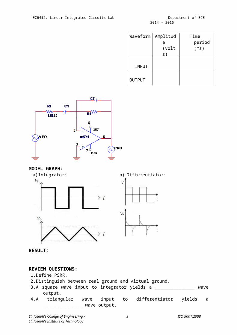
Ex. No:2 INTEGRATOR AND DIFFERENTIATOR Date:AIM:
To design and test the following Op-Amp Circuits: a. Integrator b. DifferentiatorAPPARATUS REQUIRED:
S.No. Name of the Apparatus Range/Value Qty
1. Bread Board - 12. IC Power Supply ±15 V 13. Resistor 10 k Ω, 100 k Ω,1.5 k Ω,15k Ω 2, 1,1,14. IC 741 Op-Amp - 15. CRO 20 MHz. 16. Signal Generator 0-1 MHz. 17. Capacitor 0.1µF,0.01 µF 1(each)
8. Connecting Wires - Few
THEORY:a. INTEGRATOR:The circuit performs the mathematical operation of integration, that is, the output waveform is the integral of the input waveform. The output voltage Vo(t) = - (1/RfCf) Vi(t) dt , Where Vi is the input voltage , Rf is the feedback resistance & Cf is the feedback capacitence.b. DIFFERENTIATOR:The circuit performs the mathematical operation of differentiation, that is, the output waveform is the derivative of the input waveform. The output voltage Vo(t) = - RC (dvi / dt) Where Vi is the input voltage , Rf is the feedback resistance & Cf is the feedback capacitenceDESIGN:a. Integrator: Design of Integrator with lower frequency limit of fmin = 160Hz.
Rf = 10R1
Let R1=1.5KΩ, then Rf = The range of Cf value from 0.001µF to 10µF is preferable. The capacitor has to very low leakage
b. Differentiator: Design of opamp differentiator that will differentiate an input
signal with fa =100Hz.The time period T of the input signal must be larger than or equal to RfC1.
Highest frequency of the input signal =
Select . Let
;
St. Joseph’s College of Engineering / 5 ISO 9001:2008St. Joseph’s Institute of Technology

EC6412: Linear Integrated Circuits Lab Department of ECE 2014 - 2015
R1 C1 = Rf Cf;
PROCEDURE:1. Connections are given as per the circuit diagram for integrator.2. The square wave of 2Vp-p is given as input to the inverting terminal of the IC. 3. The output waveform is observed in the CRO.4. Plot the input and output waveforms.5. Repeat the same for differentiator
CIRCUIT DIAGRAM TABULATION:a. INTEGRATOR :
b. DIFFERENTIATOR:
St. Joseph’s College of Engineering / 6 ISO 9001:2008St. Joseph’s Institute of Technology
Waveform Amplitude (Volts)
Time period (ms)
INPUT
OUTPUT
Waveform Amplitude (volts)
Time period (ms)
INPUT
OUTPUT

EC6412: Linear Integrated Circuits Lab Department of ECE 2014 - 2015
MODEL GRAPH:a) Integrator: b) Differentiator:
RESULT:
REVIEW QUESTIONS:1. Define PSRR.2. Distinguish between real ground and virtual ground.3. A square wave input to integrator yields a _______________ wave output.4. A triangular wave input to differentiator yields a _______________ wave output.5. If a square wave is given as input to a differentiator, what will be its output? Justify the answer.
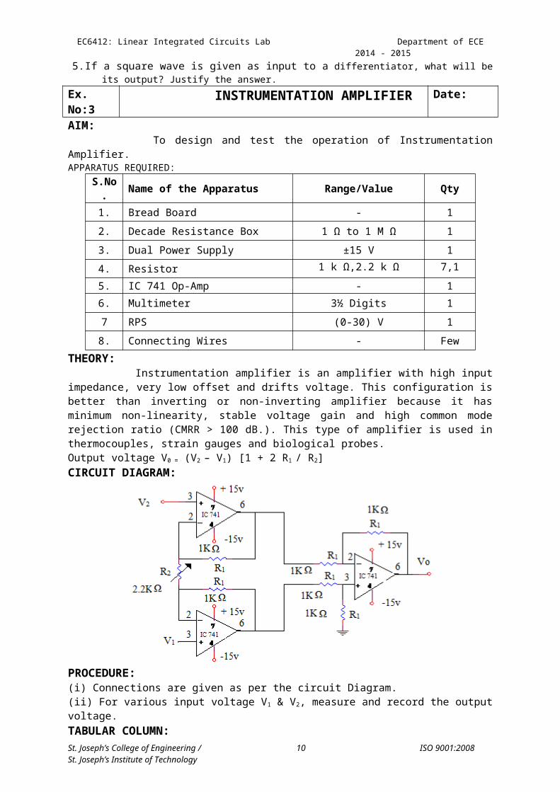
Ex. No:3 INSTRUMENTATION AMPLIFIER Date:AIM: To design and test the operation of Instrumentation Amplifier.APPARATUS REQUIRED:
S.No. Name of the Apparatus Range/Value Qty
1. Bread Board - 1
2. Decade Resistance Box 1 Ω to 1 M Ω 1
3. Dual Power Supply ±15 V 1
4. Resistor 1 k Ω,2.2 k Ω 7,1
5. IC 741 Op-Amp - 1
6. Multimeter 3½ Digits 1
7 RPS (0-30) V 1
8. Connecting Wires - Few
THEORY: Instrumentation amplifier is an amplifier with high input impedance, very low offset and
drifts voltage. This configuration is better than inverting or non-inverting amplifier because it has minimum non-linearity, stable voltage gain and high common mode rejection ratio (CMRR > 100 dB.). This type of amplifier is used in thermocouples, strain gauges and biological probes.Output voltage V0 = (V2 – V1) [1 + 2 R1 / R2]CIRCUIT DIAGRAM:
St. Joseph’s College of Engineering / 7 ISO 9001:2008St. Joseph’s Institute of Technology

EC6412: Linear Integrated Circuits Lab Department of ECE 2014 - 2015
PROCEDURE:(i) Connections are given as per the circuit Diagram.(ii) For various input voltage V1 & V2, measure and record the output voltage.TABULAR COLUMN:
R2
ohmsR1
ohmsV1
voltsV2
voltsVo in volts
Theoretical Practical
RESULT:
REVIEW QUESTIONS:1. List the important features of Instrumentation Amplifiers.2. List the commercially available Monolithic IC Instrumentation Amplifiers.3. List the applications of Instrumentation Amplifiers.4. Define: Common mode gain, Differential Mode gain.
Ex. No:4 SECOND ORDER ACTIVE FILTERS Date:AIM: To design, construct and plot the frequency response of second order low pass and high pass filter having the fc of 1 kHz.APPARATUS REQUIRED:
S.No. Name of the Apparatus Range/Value Qty
1. Bread Board - 1
2. IC Power Supply ±15 V 1
3. Resistor10 k Ω,5.86 k Ω
1.6 k Ω12
4. IC 741 Op-Amp - 1
5. CRO 20 MHz. 1
6. Function Generator 0-3MHz. 1
7. Capacitor 0.1µF 2
8. Connecting Wires - Few
St. Joseph’s College of Engineering / 8 ISO 9001:2008St. Joseph’s Institute of Technology
EC6412: Linear Integrated Circuits Lab Department of ECE 2014 - 2015
THEORY: An improved filter response can be obtained by using a second order active filter. A second order filter consist of two RC pairs has a roll-off rate of –40db/decade. The transfer function of a Low pass
filter is For n=2, the damping factor α = 1.414, the pass band gain
A0 = 3 – α = 1.586. Cutoff frequency of the filter = 1/ 2π RC= h. HPF is the complement of the Low pass filter and can be obtained simply by interchanging R and C in the low pass configurationDESIGN:
fc = 1KHz, Assume C = 0.1µF, R= 1/2πfcC= The gain for the second order filter is known as 1.5816.
Let Ri = 10KΩ, Gain =Ao = 1.5816 => 1+ Rf / Ri = 1.586 => Rf = 0.586 Ri = CIRCUIT DIAGRAM: Low Pass Filter
PROCEDURE:1. Connect the Low pass filter circuit as shown in the circuit diagram.2. Give an input signal Vi of 2V(p-p) and measure the output voltage for different frequency from the
CRO.3. Plot the frequency response 20 log Vo/Vi versus input frequency and find 3db frequency.4. Determine the cut-off frequency from the plot.5. Repeat the above for HPF.TABULATION: Low Pass Filter INPUT VOLTAGE: Vi = volts
Frequency Hz Output voltage Vo volts Gain in db 20 logVo/Vi
St. Joseph’s College of Engineering / 9 ISO 9001:2008St. Joseph’s Institute of Technology
EC6412: Linear Integrated Circuits Lab Department of ECE 2014 - 2015
High Pass Filter:
High Pass Filter: INPUT VOLTAGE: Vi = voltsFrequency Hz Output voltage Vo volts Gain in db 20 logVo/Vi
St. Joseph’s College of Engineering / 10 ISO 9001:2008St. Joseph’s Institute of Technology

EC6412: Linear Integrated Circuits Lab Department of ECE 2014 - 2015
MODEL GRAPH: Low Pass Filter: High Pass Filter:
RESULT:
LPF: i. Theoretical = ii. Practical = HPF: i. Theoretical = ii. Practical =
REVIEW QUESTIONS:1. Why are active filters preferred?2. What is the roll-off rate of a First order filter?3. Define Active Low Pass and Band Pass Filter.4. On what factors does the damping coefficient of a filter depend on?5. What is a Sallen –Kay filter?
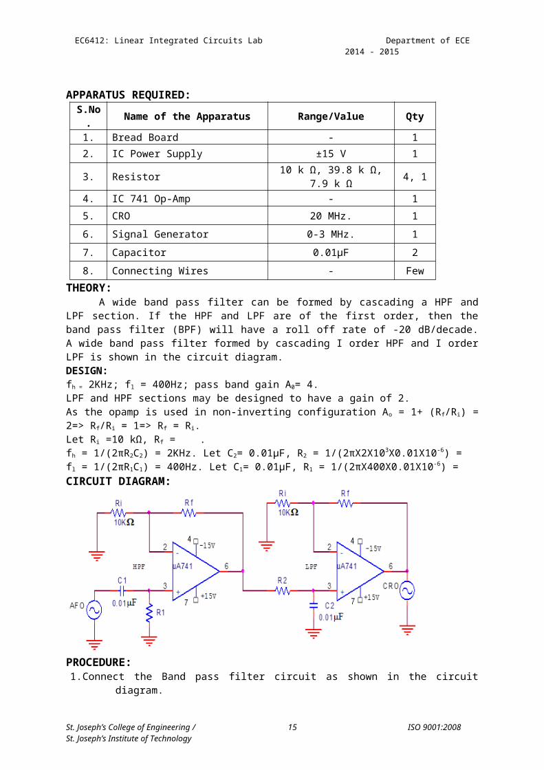
Ex. No:5 BAND PASS FILTER Date:AIM: To design, construct, test and to plot the frequency response of wide band pass filter.
APPARATUS REQUIRED:
S.No. Name of the Apparatus Range/Value Qty
1. Bread Board - 1
2. IC Power Supply ±15 V 1
3. Resistor 10 k Ω, 39.8 k Ω, 7.9 k Ω 4, 1
4. IC 741 Op-Amp - 1
5. CRO 20 MHz. 1
6. Signal Generator 0-3 MHz. 1
7. Capacitor 0.01µF 2
8. Connecting Wires - Few
THEORY:A wide band pass filter can be formed by cascading a HPF and LPF section. If the HPF and
LPF are of the first order, then the band pass filter (BPF) will have a roll off rate of -20 dB/decade. A wide band pass filter formed by cascading I order HPF and I order LPF is shown in the circuit diagram.DESIGN: fh = 2KHz; fl = 400Hz; pass band gain A0= 4. LPF and HPF sections may be designed to have a gain of 2. As the opamp is used in non-inverting configuration Ao = 1+ (Rf/Ri) = 2=> Rf/Ri = 1=> Rf = Ri.Let Ri =10 kΩ, Rf = .
St. Joseph’s College of Engineering / 11 ISO 9001:2008St. Joseph’s Institute of Technology

EC6412: Linear Integrated Circuits Lab Department of ECE 2014 - 2015
fh = 1/(2πR2C2) = 2KHz. Let C2= 0.01µF, R2 = 1/(2πX2X103X0.01X10-6) = fl = 1/(2πR1C1) = 400Hz. Let C1= 0.01µF, R1 = 1/(2πX400X0.01X10-6) = CIRCUIT DIAGRAM:
PROCEDURE:1. Connect the Band pass filter circuit as shown in the circuit diagram.2. Give an input signal Vi of 1V (p-p) and measure the output voltage for different frequency.3. Plot the frequency response 20 log Vo/Vi versus input frequency and find 3db frequency.4. Determine the cut-off frequency fh and fl .
MODEL GRAPH:
TABULATION: INPUT VOLTAGE: Vi = voltsFrequency ( Hz ) Output voltage Vo (volts) Gain in db 20 logVo/Vi
St. Joseph’s College of Engineering / 12 ISO 9001:2008St. Joseph’s Institute of Technology

EC6412: Linear Integrated Circuits Lab Department of ECE 2014 - 2015
RESULT:
Lower cutoff frequency: i. Theoretical = ii. Practical = Upper cutoff frequency: i. Theoretical = ii. Practical =
REVIEW QUESTIONS:1.Why are active filters preferred?2.What is the roll-off rate of a First order filter?3.On what factors does the damping coefficient of a filter depend on?4.How a Notch filter is obtained from a band pass filter?5.How a low pass filter is transformed into a high pass filter?
Ex. No:6 ASTABLE MULTIVIBRATOR USING OP-AMP IC 741.
Date:
AIM: To design a square wave generator for fo = 1kHz and study its performance.APPARATUS REQUIRED:
S.No. Name of the Apparatus Range/Value Qty
1. Bread Board - 12. IC Power Supply ±15 V 1
3. Resistor 10KΩ, 11.6KΩ 2, 1
4. IC 741 Op-Amp - 15. CRO 20MHz. 17. Capacitor-DCB 0.05µF 18. Connecting Wires - Few
THEORY: Square wave outputs are generated when the opamp is forced to operate in the saturated
region. That is, the output of the opamp is forced to swing repetitively between positive saturation V sat and negative saturation –Vsat, resulting in the square wave output. Astable multivibrator circuit is shown in figure. The output of the opamp in this circuit will be in positive or negative saturation, depending whether the differential voltage is positive or negative, respectively. The time period T of the output wave form is T = 2 RC ln ((1+β)/(1-β)) where β=R2/(R1+R2). If R1 = 1.16 R2, T = 2RC and frequency = 1/(2RC).DESIGN: f0 = 1KHzR1 = 1.16R2, Let R2 = 10KΩ => R1 = Let C= 0.05µF => R = 1/ (10 X10-8X1000) = CIRCUIT DIAGRAM:
St. Joseph’s College of Engineering / 13 ISO 9001:2008St. Joseph’s Institute of Technology

EC6412: Linear Integrated Circuits Lab Department of ECE 2014 - 2015
PROCEDURE:1. Connect the circuit as shown in the circuit diagram using component values as obtained in design.2. Observe and sketch the capacitor voltage wave form and output wave form. 3. Determine the frequency and plot the graph.TABULATION:
Tlow (ms) Thigh (ms) Frequency (Hz) Output Voltage (V)
Capacitor Voltage (V)
Practical Theoretical Practical Theoretical Practical Theoretical
MODEL GRAPH:
RESULT:
REVIEW QUESTIONS:1. Give the other name for Astable Multivibrator.2. Write the principle of Astable Multivibrator.3. What will be the peak to peak output voltage of Astable Multivibrator?4. How to generate an asymmetrical square wave from Astable Multivibrator?5. List the applications of Astable Multivibrator.
Ex. No:7 MONOSTABLE MULTIVIBRATOR USING OP-AMP IC 741.
Date:
AIM: To design, construct and test a monostable multivibratorAPPARATUS REQUIRED:
S.No. Name of the Apparatus Range/Value Qty
St. Joseph’s College of Engineering / 14 ISO 9001:2008St. Joseph’s Institute of Technology
EC6412: Linear Integrated Circuits Lab Department of ECE 2014 - 2015
1. Bread Board - 1
2. IC Power Supply ±15 V 1
3. Resistor 1KΩ, 8.2KΩ 3, 1
4. IC 741 Op-Amp - 1
5. CRO 20 MHz. 1
6. Function Generator 0-1 MHz. 1
7. Capacitor 0.1µF 2
9. Diode - 2
8. Connecting Wires - Few
THEORY:Monostable multivibrator is a square wave shaping circuit having one stable state and another
quasi stable state. It can be made to switch to other state by the application of triggering pulse, but it then returns to its stable state after a time interval determined the RC value. It is often referred as single shot multivibrator. It is also used as a gating circuit and delay circuit. The time period is T = RC ln ((1+VD / Vsat)/ (1-)) Where = R2 / (R1+R2), VD is diode cut-in Voltage and Vsat = 15VIf Vsat >> VD and R1= R2 so that = 0.5, then T =0.69RC.DESIGN:
T= 600µs, Assume C= 0.1 µF; T =0.69RC Let R1= R2=1k Ω; C= C4= 0.1 µF; R = 600X106/(0.69X0.1X10-6) =
CIRCUIT DIAGRAM:
PROCEDURE:1. The connection is made as per the circuit diagram.2. Apply a negative going pulse as the input signal.3. Observe the output voltage across the capacitor Vc and the output waveform V0 and trace it.
TABULATION:
Resistance R(KHz) Capacitor C (μF) Time Period T(ms) Frequency KHZ
WAVEFORM:
St. Joseph’s College of Engineering / 15 ISO 9001:2008St. Joseph’s Institute of Technology

EC6412: Linear Integrated Circuits Lab Department of ECE 2014 - 2015
RESULT:
i. Theoretical = Practical =REVIEW QUESTIONS:1. State the two states of Monostable Multivibrator.2. How is the width of the output pulse adjusted in a Monostable Multivibrator?3. For Monostable operation, the trigger pulse width Tp should be _________ than T, the pulse width.4. Give the other name for Monostable Multivibrator.5. List the applications of Astable and Monostable Multivibrator.Ex. No:8 SCHMITT TRIGGER (REGENERATIVE
COMPARATOR)Date:
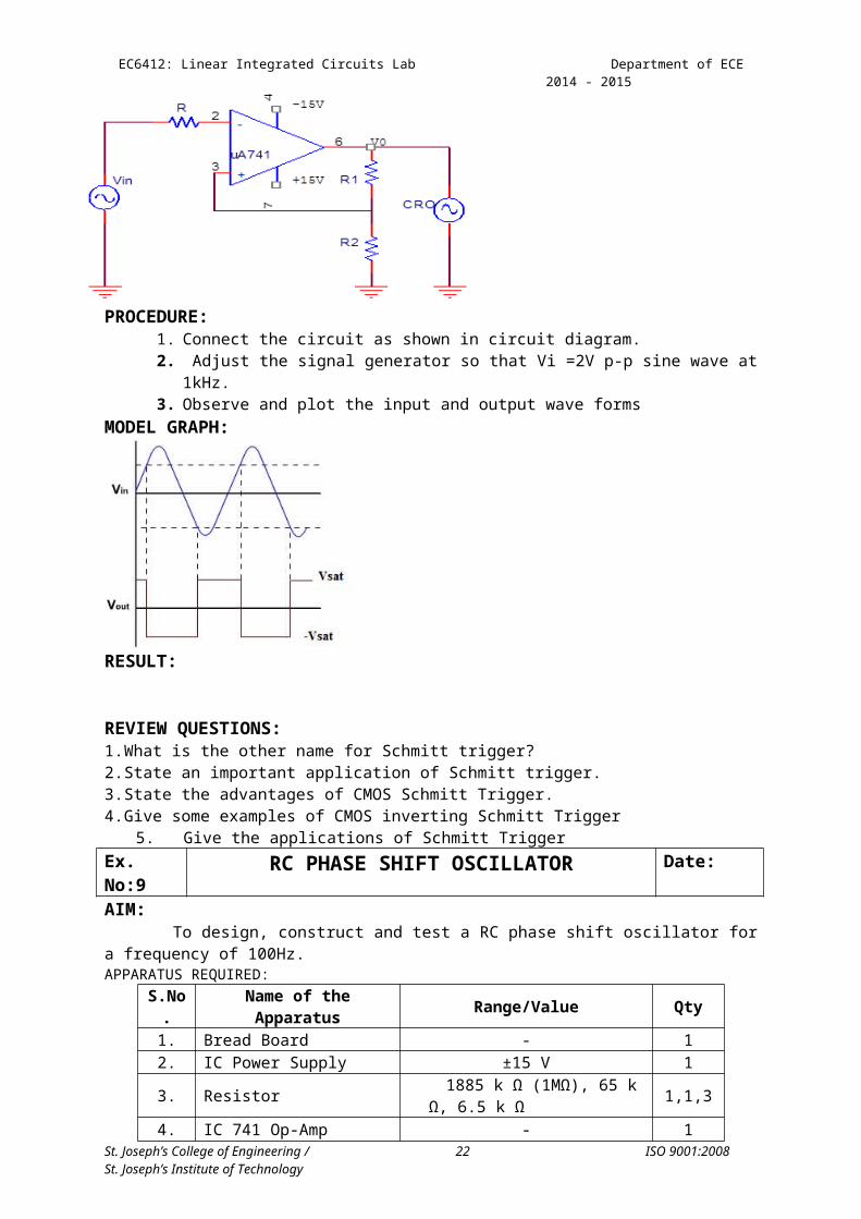
AIM: To design a Schmitt trigger circuit for generating a square wave output. APPARATUS REQUIRED:
S.No. Name of the Apparatus Range/Value Qty
1. Bread Board - 1
2. IC Power Supply ±15 V 1
3. Resistor 1 k Ω, 27 k Ω 2, 1
4. IC 741 Op-Amp - 1
5. CRO 20 MHz. 1
6. Function Generator 0-3 MHz. 1
7. Connecting Wires - Few
THEORY: Schmitt trigger circuit is an inverting comparator with positive feed back. The input voltage
is applied to the (-) terminal and feed back voltage to the (+) terminal. The input voltage V i triggers the output every time it exceeds certain voltage levels called upper threshold and lower threshold voltage. This circuit converts an irregular shaped wave form to a square wave or pulse. The upper and lower threshold is VUT = Vsat [R2/(R1+R2)], VLT = - Vsat [R2/(R1+R2)] respectively.DESIGN: VUT = + 0.5V; VLT = - 0.5VFor 741, with supply voltages ±15V, the saturation voltage ±V sat = ±15V0.5 = 15 [R2/ (R1+R2)]. R1=27 R2. Let R2 = 1 kΩ therefore R1 = CIRCUIT DIAGRAM: TABULATION:
St. Joseph’s College of Engineering / 16 ISO 9001:2008St. Joseph’s Institute of Technology
EC6412: Linear Integrated Circuits Lab Department of ECE 2014 - 2015
PROCEDURE:1. Connect the circuit as shown in circuit diagram.2. Adjust the signal generator so that Vi =2V p-p sine wave at 1kHz.3. Observe and plot the input and output wave forms
MODEL GRAPH:
RESULT:
REVIEW QUESTIONS:1. What is the other name for Schmitt trigger?2. State an important application of Schmitt trigger.3. State the advantages of CMOS Schmitt Trigger.4. Give some examples of CMOS inverting Schmitt Trigger
5. Give the applications of Schmitt TriggerEx. No:9 RC PHASE SHIFT OSCILLATOR Date:AIM: To design, construct and test a RC phase shift oscillator for a frequency of 100Hz.APPARATUS REQUIRED:
S.No. Name of the Apparatus Range/Value Qty
1. Bread Board - 12. IC Power Supply ±15 V 1
3. Resistor 1885 k Ω (1MΩ), 65 k Ω, 6.5 k Ω 1,1,3
4. IC 741 Op-Amp - 1
5. CRO 20 MHz. 16. Capacitor 0.1µF, 0.01µF 3, 1
St. Joseph’s College of Engineering / 17 ISO 9001:2008St. Joseph’s Institute of Technology
Waveform Amplitude (Volts)
Time period (ms)
INPUT
OUTPUT

EC6412: Linear Integrated Circuits Lab Department of ECE 2014 - 2015
7. Connecting Wires - Few
THEORY: Oscillator is a feed back circuit where a fraction of output voltage of an amplifier is fed back to the input in the same phase. RC phase shift oscillators are sine wave oscillators which are used in the audio frequency range. The amplification is done by the op-amp and as it is used in the inverting mode is gives a phase shift of 180 .The feedback RC network produces an additional phase shift of 180.Each RC network gives 60 phase shift.
The frequency of oscillation is given by = 1/6(2RC)DESIGN:fo = 100Hz; Assume C = 0.1 µF => R = 1/6(2foC) = 1/6(2X100X0.1X10-6) = To prevent overloading of the amplifier by RC network, R1 ≤ 10RLet R1 = 10R = Rf = 29 R1 = CIRCUIT DIAGRAM:
PROCEDURE: 1. The connection is made as per the circuit diagram. 2. Observe the output waveform V0 and calculate the frequency of oscillation. 3. Plot the waveform.TABULATION:
OUTPUT VOLTAGE (V) TIME PERIOD(ms) FREQUENCY OF
OSCILLATION (KHZ)
MODEL GRAPH:
T= One cycle time, F=Frequency of wave in Hz=1/TRESULT:
i. Theoretical = ii. Practical =REVIEW QUESTIONS:1. Write the conditions necessary for Sustained Oscillations.2. List the two types of AF RC Oscillators.3. In RC phase shift oscillator, the gain of Inverting Op-Amp should be.4. Write the expression for output frequency in a RC Phase shift oscillator.St. Joseph’s College of Engineering / 18 ISO 9001:2008St. Joseph’s Institute of Technology

EC6412: Linear Integrated Circuits Lab Department of ECE 2014 - 2015
5. List the applications of RC Phase shift oscillator.
Ex. No:10 WEIN BRIDGE OSCILLATOR Date:AIM: To design the wein’s bridge oscillator using OP-AMP IC for f0 = 1000Hz APPARATUS REQUIRED:
S.No. Name of the Apparatus Range/Value Qty
1. Bread Board - 12. IC Power Supply ±15 V 1
3. Resistor 100 k Ω POT, 3 k Ω, 30 k Ω 1,2,14. IC 741 Op-Amp - 15. CRO 20 MHz. 1
6. Capacitor - DCB 0.05 µF 2 THEORY: The Wein bridge oscillator is the most commonly used audio frequency oscillator because of its simplicity and stability. The bridge has a series RC network in one arm and a parallel RC network in the adjoining arm. In the remaining two arms of the bridge, resistors R 1 and Rf are connected. The phase angle criterion for oscillation is that the total phase shift around the circuit must be 0. This condition occurs only when the bridge is balanced. The frequency of oscillation f0 is exactly the resonant frequency of the balanced Wein bridge and is given by, Frequency = f0 = 1/ (2πRC).DESIGN:f0=1KHz; f0 = 1/(2πRC)=> R = 1/(2πf0C), Choose C=0.05FR= 1/(2πX1X103X0.05X10-6) => R = Take R1=10R= Rf = 2R1 = CIRCUIT DIAGRAM:
PROCEDURE: 1. Construct the circuit with the values obtained in the design.2. Observe the output waveform on an Oscilloscope. Adjust Rf to obtain a sine wave output.3. Measure the frequency of oscillator and voltage amplitude. Plot the output.
TABULATION:OUTPUT VOLTAGE (V) TIME PERIOD (ms) Frequency of Oscillation (KHz)
St. Joseph’s College of Engineering / 19 ISO 9001:2008St. Joseph’s Institute of Technology

EC6412: Linear Integrated Circuits Lab Department of ECE 2014 - 2015
MODEL GRAPH:
RESULT:
i. Theoretical = ii. Practical =REVIEW QUESTIONS:1. What is Oscillator?2. Write the expression for output frequency in a Wien Bridge oscillator.3. In a Wien Bridge Oscillator, what should be the gain of the amplifier for sustained oscillations?4. Classify the Oscillators based on their frequencies5. List the applications of Wien Bridge oscillator
Ex. No:11 DESIGN OF ASTABLE MULTIVIBRATOR USING IC 555 TIMER
Date:
AIM: To design and test an astable multivibrator for generating symmetrical and unsymmetrical square wave form for the given frequency and duty cycle.APPARATUS REQUIRED:
S. No. Name of the Apparatus Range/Value Qty
1. Bread Board - 1
2. Resistor 3.6 k Ω, 7.2 k Ω 1, 2
3. IC 555 - 1
4. CRO 20 MHz. 1
5. Capacitor 0.1µF, 0.01µF 1, 1
6. RPS (0-30) V/ 5V 1
7. Diode 18. Connecting Wires - Few
THEORY: The 555 timer is connected as an astable multivibrator as shown in figure. In this mode of operation the timing capacitor charges up towards Vcc (assuming Vo is high initially) through (Ra + Rb) until the voltage across the capacitor reaches the threshold level (2/3) Vcc. At this point the internal upper comparator switches state causing the internal flip-flop output to go high. This turns on the discharge transistor and the timing capacitor C then discharges through Rb and the discharging transistor. The discharging continues until the capacitor voltage drops to (1/3) V cc at which point the internal lower comparator switches states causing the internal flip-flop output to go low, turning off the discharge transistor. At this point the capacitor starts to charge again, thus completing the cycle.DESIGN: i. For Unsymmetrical waveform: f =1/T=1.44/(Ra+2Rb)C;DutyCycle = D = tlow/ ( tlow + t high ) => D= R b/ (Ra +2Rb) ;Where thigh = 0.693(Ra + R b)C; tlow = 0.69; Specifications: frequency = 1kHz; Duty cycle = 25% Design: tlow = 0.25ms = 0.693R b C; Let C= 0.1µF => R b = 0.25/(0.693X0.1X10-6) = thigh = 0.693(Ra + R b)C = 0.75 ms => Ra = ii. For Symmetrical Wave form :
St. Joseph’s College of Engineering / 20 ISO 9001:2008St. Joseph’s Institute of Technology

EC6412: Linear Integrated Circuits Lab Department of ECE 2014 - 2015
thigh = 0.693 Ra C; tlow = 0.693 R bC f = 1/T = 1.44 /(Ra + Rb)C => D= Rb /(Ra + Rb); Specifications: frequency = 1 kHz; Duty cycle = 50% .Design: tlow = 0.5 ms = 0.693 R bC; Let C= 0.1 µF; R b =thigh = 0.693 Ra C = 0.5 ms ; Ra =CIRCUIT DIAGRAM: Unsymmetrical: Symmetrical:
St. Joseph’s College of Engineering / 21 ISO 9001:2008St. Joseph’s Institute of Technology
PROCEDURE:1. Connect the circuit as given using component values as obtained in designed part (i)2. Observe and sketch the capacitor voltage waveform and output waveform.3. Measure the frequency and duty cycle of the output waveform.4. Connect the circuit using component values as obtained from designed part (ii).5. Repeat step 2 and 3 TABULATION:Symmetrical: Duty Cycle = 50 %
tlow (ms) t high (ms) Frequency (Hz)Output
Voltage (V)Capacitor
Voltage (V)Theoretical Practical Theoretical Practical Theoretical Practical
Unsymmetrical: Duty Cycle = 25%
tlow (ms)t high (ms) Frequency (Hz)
Output Voltage (V)
Capacitor Voltage (V)
Theoretical Practical Theoretical Practical Theoretical Practical
MODEL GRAPH:
RESULT:
REVIEW QUESTIONS:1. List the Characteristics of IC 555 timer.2. List two available packages of IC 555.3. With which type of Logic circuits, IC 555 is compatible?4. What is the range of supply voltage over which IC 555 works?5. List the applications of IC 555.
Ex. No:12 MONOSTABLE MULTIVIBRATOR USING IC 555 TIMER
Date:
AIM:To design, construct and test a monostable multivibrator using IC - 555 timer.
APPARATUS REQUIRED:
S. No. Name of the Apparatus Range/Value Qty
1. Bread Board - 1
2. Resistor 1.8 k Ω 1
3. IC 555 - 1
4. CRO 20 MHz. 1

5. Function Generator 0-3 MHz. 1
6. Capacitor 0.1µF, 0.01µF 1, 1
7. RPS (0-30) V/ 5V 1
8. Connecting Wires - Few
THEORY:Mono-stable multivibrator has only one stable state and one quasi-stable state. Transition is
obtained from the stable to quasi-stable by triggering. The transition time due to external triggering is very short, whereas the time for the circuit to remain quasi-stable state is very large. The circuit returns to stable state from its quasi-stable state by itself, without requiring any external triggering signal. Because, after triggering, the circuit returns from quasi-stable state by itself after a certain time delay, therefore the circuit is also called a one shot multivibrator or univibrator.
The mono-stable multivibrator is a regenerative device, which is used to generate rectangular output, pulse of predetermined width. The device can make a fast transition in time T after the application of input trigger and as such can be used as a delay circuit. The circuit is also referred to as gating circuit, because it generates rectangular wave form, which can be used to gate other circuits. The Pulse width is T = 1.1 RC, where R is the resistor and C is the capacitor. DESIGN:T=1.1 RC;Let T = 200 µsec; C= 0.1µF => R = CIRCUIT DIAGRAM:
PROCEDURE:1. Connect the circuit as shown in circuit diagram. 2. Apply negative trigger to pin 2. 3. Observe and sketch the output wave form at pin 3.4. Observe the output pulse width for different values of C and tabulate.
TABULATION:R (k Ω) C (F ) Pulse width
T (Practical) (ms)Pulse width
T (Theoretical) (ms)
MODEL GRAPH:

RESULT:
REVIEW QUESTIONS:1. Write the expression for timing interval of IC 555 Timer Monostable operation.2. Write the applications of Monostable mode operation of IC 555.3. Write the applications of Astable mode operation of IC 555.4. What are the modes of operation of a Timer?5. Define Duty Cycle.
Ex. No:13 PLL (IC 565) CHARACTERISTICS AND ITS USEAS FREQUENCY MULTIPLIER
Date:
AIM:a. To study the characteristics of a Phase Locked Loop (PLL)-IC 565. b. To study the frequency multiplier circuit using PLL-IC 565.
THEORY:a) PLL- It is basically a feedback control system that controls the phase of a voltage controlled
oscillator (VCO). The input signal is applied to one input of a phase detector. The other input is connected to the output of VCO. Normally the frequencies of both signals will be nearly the same. The output of the phase detector is a voltage proportional to the phase difference between the two inputs. This signal is applied to the loop filter. It is the loop filter that determines the dynamic characteristics of the PLL. The filtered signal controls the VCO. The output of the VCO is applied to the phase detector. Normally the loop filter is designed to match the characteristics required by the application of the PLL. If the PLL is to acquire and track a signal the bandwidth of the loop filter will be greater than if it expects a fixed input frequency. The frequency range which the PLL will accept and lock on is called the capture range. Once the PLL is locked and tracking a signal the range of frequencies that the PLL will follow is called the tracking range. Generally the tracking range is larger than the capture range. Figure shows the block diagram of PLL
Reference Signal Source
Phase Frequency Detector
Loop Filter
Voltage Controlled Oscillator
Oscillator Output

b) Frequency multiplier using the 565 PLL- The frequency divider is inserted between the VCO and the phase comparator. Since the output of the divider is locked to the input frequency f in, the VCO is actually running at a multiple of the input frequency. The desired amount of multiplication can be obtained by selecting a proper divide by N network, where N is an integer. For example, to obtain the output frequency fOUT = 5 fin, a divide by N = 5 network is needed. The 4 bit binary counter (7490) is configured as a divide by 5 circuits. The transistor Q is used as a driver stage to increase the driving capability of the NE 565. C3 is used to eliminate possible oscillation. C2 should be large enough to stabilize the VCO frequency.
DESIGN: a. PLL Circuit The Circuit components are R1 = 12 KΩ, C1 =0.01 µF, C2 =10 µF & C3 =0.001 µF. The design formulae are: V= (+V)-(-V) = 20 Volt. Free running frequency, f out= 1.2 / [4 R1 C1 ] = 2.5 KHz. Lock Range, fL= ± 8 X fout / V = ± 1 KHz. Capture Range, fc= ± fL / [2 π X 3.6 X 103 X C2] = ± 66.49 Hz
CIRCUIT DIAGRAM: a. PLL Circuit
b. Frequency Multiplier
Phase Comparator Amplifier LPF
Voltage Controlled Oscillator
VCOfin
Fin = fout / N

RESULT:
REVIEW QUESTIONS:1. What are the building blocks of PLL?2. What is VCO? Explain.3. Which determines the frequency of VCO?4. What is the use of LPF in PLL?5. Define Lock in range and Capture range.
Ex. No:14 IC REGULATED DC POWER SUPPLY USING LM 723 and LM 317
Date:
AIM:To design the regulated DC power supply using LM 723 and LM 317.
APPARATUS REQUIRED:
S. No. Name of the Apparatus Range/Value Qty
1. Bread Board - 1
2. Resistor 5 KΩ, 240Ω 1
3. NE 565 , IC 7490 - 1 each
4. Voltmeter (0 – 30)V 1
6. Capacitor 10µF, 0.1µF, 0.100pF 1 each
7. RPS (0-30) V/ 5V 1
8. Connecting Wires - Few
THEORY:

A voltage regulator is designed to automatically maintain a constant voltage level. A voltage regulator may be a simple "feed-forward" design or may include negative feedback control loops. It may use an electromechanical mechanism, or electronic components. Depending on the design, it may be used to regulate one or more AC or DC voltages. Electronic voltage regulators are found in devices such as computer power supplies where they stabilize the DC voltages used by the processor and other elements. In automobile alternators and central power station generator plants, voltage regulators control the output of the plant. In an electric power distribution system, voltage regulators may be installed at a substation or along distribution lines so that all customers receive steady voltage independent of how much power is drawn from the line. The circuit diagram shows an IC 723 connected to operate as a positive voltage regulator. The output voltage can be set to any value between approximately 7 V (reference voltage) and 37 V by appropriate selection of resistors R1 and R2. A potentiometer may be included between R1 and R2, of course, to make the voltage adjustable. An external transistor may be Darlington connected to Q 1
(as shown in earlier post) to handle large load current.
DESIGN:a) REGULATOR USING LM317Vout = 6V (given). Vout = 1.25[1+R2/R1]Let R2 = 240Ω, R1 = R2/(0.8XVout-1) =
b)REGULATOR USING LM723
Vout = 3V (given). .
Vref = 7V. Choose R1+R2=10K Ω, C1 = 100pF.
=
PROCEDURE:1. Connect the circuit as shown in circuit diagram. 2. Apply the unregulated power supply at pin 3. 3. Vary the voltage and observe the regulated output and tabulate the reading.4. Plot the graph.
CIRCUIT DIAGRAM:REGULATOR USING LM317 TABULATION:
REGULATOR USING LM 723:
S.No. Vin in Volts Vout in Volts

RESULT:
REVIEW QUESTIONS:1. What are the major blocks of series Op-Amp regulator?2. Write the function of a Voltage regulator.3. What is Voltage reference? Why is it needed?4. What are the voltage options available in 78XX and 79XX Voltage regulators?5. What are the limitations of 3-terminal voltage regulators?
Ex. No:15 STUDY OF SMPS Date:AIM:To study the switched mode power supplyTHEORY:
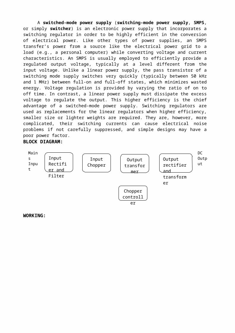
A switched-mode power supply (switching-mode power supply, SMPS, or simply switcher) is an electronic power supply that incorporates a switching regulator in order to be highly efficient in the conversion of electrical power. Like other types of power supplies, an SMPS transfer’s power from a source like the electrical power grid to a load (e.g., a personal computer) while converting voltage and current characteristics. An SMPS is usually employed to efficiently provide a regulated output voltage, typically at a level different from the input voltage. Unlike a linear power supply, the pass transistor of a switching mode supply switches very quickly (typically between 50 kHz and 1 MHz) between full-on and full-off states, which minimizes wasted energy. Voltage regulation is provided by varying the ratio of on to off time. In contrast, a linear power supply must dissipate the excess voltage to regulate the output. This higher efficiency is the chief advantage of a switched-mode power supply. Switching regulators are used as replacements for the linear regulators when higher efficiency, smaller size or lighter weights are required. They are, however, more complicated, their switching currents can cause electrical noise problems if not carefully suppressed, and simple designs may have a poor power factor.BLOCK DIAGRAM:
S.No. Vin in Volts Vout in Volts
DC OutputInput
Rectifier and Filter
Input Chopper
Output transformer
Output rectifier and transformer
Chopper controller
MainsInput

WORKING:INPUT RECTIFIER STAGE
If the SMPS has an AC input, then the first stage is to convert the input to DC. This is called rectification. The rectifier circuit can be configured as a voltage doubler by the addition of a switch operated either manually or automatically. This is a feature of larger supplies to permit operation from nominally 120 V or 240 V supplies. The rectifier produces an unregulated DC voltage which is then sent to a large filter capacitor. The current drawn from the mains supply by this rectifier circuit occurs in short pulses around the AC voltage peaks. These pulses have significant high frequency energy which reduces the power factor. Special control techniques can be employed by the following SMPS to force the average input current to follow the sinusoidal shape of the AC input voltage thus the designer should try correcting the power factor. An SMPS with a DC input does not require this stage.
An SMPS designed for AC input can often be run from a DC supply (for 230 V AC this would be 330 V DC), as the DC passes through the rectifier stage unchanged. It's however advisable to consult the manual before trying this, though most supplies are quite capable of such operation even though nothing is mentioned in the documentation. However, this type of use may be harmful to the rectifier stage as it will only use half of diodes in the rectifier for the full load. This may result in overheating of these components, and cause them to fail prematurely. If an input range switch is used, the rectifier stage is usually configured to operate as a voltage doubler when operating on the low voltage (~120 V AC) range and as a straight rectifier when operating on the high voltage (~240 V AC) range.INVERTER STAGE (CHOPPER)
The inverter stage converts DC, whether directly from the input or from the rectifier stage described above, to AC by running it through a power oscillator, whose output transformer is very small with few windings at a frequency of tens or hundreds of kilohertz (kHz). The frequency is usually chosen to be above 20 kHz, to make it inaudible to humans. The output voltage is optically coupled to the input and thus very tightly controlled. The switching is implemented as a multistage (to achieve high gain) MOSFET amplifier. MOSFETs are a type of transistor with a low on-resistance and a high current-handling capacity. VOLTAGE CONVERTER AND OUTPUT RECTIFIER
If the output is required to be isolated from the input, as is usually the case in mains power supplies, the inverted AC is used to drive the primary winding of a high-frequency transformer. This converts the voltage up or down to the required output level on its secondary winding. The output transformer in the block diagram serves this purpose. If a DC output is required, the AC output from the transformer is rectified. For output voltages above ten volts or so, ordinary silicon diodes are commonly used. For lower voltages, Schottky diodes are commonly used as the rectifier elements; they have the advantages of faster recovery times than silicon diodes (allowing low-loss operation at higher frequencies) and a lower voltage drop when conducting. For even lower output voltages, MOSFETs may be used as synchronous rectifiers; compared to Schottky diodes, these have even lower conducting state voltage drops. The rectified output is then smoothed by a filter consisting of inductors and capacitors. For higher switching frequencies, components with lower capacitance and inductance are needed. REGULATION
A feedback circuit monitors the output voltage and compares it with a reference voltage, which shown in the block diagram serves this purpose. Depending on design/safety requirements, the controller may contain an isolation mechanism (such as opto-couplers) to isolate it from the DC output. Switching supplies in computers, TVs and VCRs have these opto-couplers to tightly control the output voltage.SMPS IC:

RESULT:
REVIEW QUESTIONS:1.What is SMPS?2. Explain the working of SMPS.3. Give the advantages of SMPS.4. Give the SMPS IC number.5. Explain the working of rectifier.
SIMULATION EXPERIMENTS USING PSPICE
INTRODUCTION:PSpice is the acronym for personal SPICE, which is acronym for simulation program with
integrated circuit emphasis. It is a type of program for simulating analog and digital circuits.
The type of simulation performed by PSpice depends on the source specifications and control statements. The types of analysis usually executed in the PSpice program are as follows:
1. DC Analysis:- it is used for circuits with time – invariant sources (e.g., steady state dc sources). It calculates all nodal voltages and branch currents over a range of values. The types of analysis and their corresponding. (dot) commands are described below:
2. Transient Analysis:- It is used for circuits with time variant sources (e.g., ac sources/switched dc sources). It calculates all nodes voltages and branch currents over a time interval and their instantaneous values are the outputs. The corresponding. (dot) commands are as follows:
3. AC Analysis:- It is used for small signal analysis of circuits with sources of varying frequencies. It also calculates all nodal voltages and branch currents (over a range of frequencies) and their magnitudes and phase angles.
In PSpice, the circuit is first described to a computer by using a file called circuit file. It contains the circuit details, viz., the information about source and commands for what to do and what to display as output. The PSpice accepts circuit file as an input and after executing commands, creates and outputs file to store results. However, the circuit to be analyzed is specified in terms of element names, element values different sources (voltage or current) and different parameters.
PSpice calculates all nodal voltages and branch currents over a range of time interval by giving the output of their instantaneous values. It can also perform other operations as will be evident later. For circuits with variable frequency sources, AC analysis is used. Each circuit element is connected between two nodes. All nodes must be connected to at least two elements and therefore appear twice at least.
OrCAD PSpice simulates analog-only circuits. After the preparation of a design for simulation, OrCAD Capture generates a circuit file set. The circuit file set, containing the circuit netlist and analysis commands, is read by PSpice for simulation.
PSpice formulates these into meaningful graphical plots, which can be marked for display directly from schematic page using markers.
OrCAD® offers a total solution for core design tasks, schematic- and VHDL-based design entry; FPGA and CPLD design synthesis; digital, analog, and mixed-signal simulation; and printed circuit board layout.

Ex. No:1 INSTRUMENTATION AMPLIFIER Date:AIM: To simulate an instrumentation amplifier using Pspice and to plot their waveform.SOFTWARE REQUIRED:PC with Pspice software.CIRCUIT DIAGRAM:
R 1
1k
uA 7413
2
74
6
+
-
..
.
R 1
1 k
+15V
+15V
+15V
R 1
1k
V1
uA 741
3
2
74
6
+
-
..
.
-15V
-15V
R 2
2 . 2 k
-15V
V2
R 1
1k
V0
R 1
1k
R 1
1 k
uA 7413
2
74
6
+
-
..
.
INSTRUMENTATION AMPLIFIER
PROCEDURE:1. Open Orcade Capture Lite edition.2. Go to file option in the main menu and select new project.3. Go to place part and select the components and place in the schematic window.4. Add wires to all the components and specify the values of the components.5. Go to Pspice in the main menu and check for errors in the netlist and set up the simulation profile by
adding required traces.6. Observe the output waveformRESULT:
REVIEW QUESTIONS:1. List the important features of Instrumentation Amplifiers.2. List the commercially available Monolithic IC Instrumentation Amplifiers.3. List the applications of Instrumentation Amplifiers.4. Write the expression for figure of merit ρ for a differential amplifier.5. Define: Common mode gain, Differential Mode gain.Ex. No:2 SECOND ORDER ACTIVE FILTERS Date:AIM: To simulate a second order Low pass filter & high pass filter using Pspice and to obtain their frequency response.SOFTWARE REQUIRED:PC with Pspice software.CIRCUIT DIAGRAM: Low Pass Filter

High Pass Filter:
PROCEDURE:Follow the same procedure as in the first experiment.RESULT:
REVIEW QUESTIONS:1. Why are active filters preferred?2. What is the roll-off rate of a First order filter?3. Define Active Low Pass and Band Pass Filter.4. On what factors does the damping coefficient of a filter depend on?5. What is a Sallen –Kay filter?
Ex. No:3 ACTIVE BAND PASS FILTER Date:
AIM: To design and simulate a band pass filter using Pspice and to obtain the frequency response.SOFTWARE REQUIRED:System with Pspice software.CIRCUIT DIAGRAM:
PROCEDURE:Follow the same procedure as in the first simulation experiment.RESULT:

REVIEW QUESTIONS:1. Define Active Low Pass and Band Pass Filter.2. On what factors does the damping coefficient of a filter depend on?3. What is a Sallen –Kay filter?4. How a Notch filter is obtained from a band pass filter?5. How a low pass filter is transformed into a high pass filter?6. Draw the frequency response of First order Low pass and High pass Filters.
Ex. No:4 ASTABLE MULTIVIBRATOR(USING OP-AMP AND IC 555 TIMER)
Date:
AIM: To simulate an astable multivibrator using Pspice.APPARATUS REQUIRED:System with Pspice software.PROCEDURE:Follow the same procedure as in the first simulation experiment.CIRCUIT DIAGRAM: Using Op-Amp
Using 555 Timer
RESULT:
REVIEW QUESTIONS:1. Give the other name for Astable Multivibrator.2. Write the principle of Astable Multivibrator.3. What will be the peak to peak output voltage of Astable Multivibrator?4. How to generate an asymmetrical square wave from Astable Multivibrator?5. List the applications of Astable Multivibrator.
Ex. No:5 SCHMITT TRIGGER Date:AIM: To design and simulate a Schmitt trigger using Pspice.SOFTWARE REQUIRED:System with Pspice software.

CIRCUIT DIAGRAM:
PROCEDURE: Follow the same procedure as in the first simulation experiment. RESULT:
REVIEW QUESTIONS:1. What is the other name for Schmitt trigger?2. State an important application of Schmitt trigger.3. State the advantages of CMOS Schmitt Trigger.4. Give some examples of CMOS inverting Schmitt Trigger5. Give the applications of Schmitt Trigger
Ex. No:6 MONOSTABLE MULTIVIBRATOR Date:AIM: To simulate monostable multivibrator using Pspice and to observe the waveforms.SOFTWARE REQUIRED:Sytsem with Pspice software.CIRCUIT DIAGRAM:
CIRCUIT DIAGRAM USING 555 TIMER

PROCEDURE:Follow the same procedure as in the first simulation experiment.RESULT:
REVIEW QUESTIONS:1 Give the application of monostable multivibrator and give its other name.2 What does MODEL D represent in pspice?3 What is the command used to end the program in pspice?4 State the two states of Monostable Multivibrator.5 How is the width of the output pulse adjusted in a Monostable Multivibrator?
Ex. No:7 RC PHASE SHIFT OSCILLATOR Date:AIM: To design and simulate RC Phase shift Oscillator using Pspice and to observe the waveform.SOFTWARE REQUIRED:Sytem with Pspice software.
CIRCUIT DIAGRAM:
PROCEDURE:Follow the same procedure as in the first simulation experiment.RESULT:
REVIEW QUESTIONS:1. How is the phase shift criteria satisfied in phase shift oscillator?2. How to represent opamp in pspice?3. What does .LIB indicate in pspice ?4. What is the type of RC oscillators?5. What are oscillation criteria?
Ex. No:8 WEIN BRIDGE OSCILLATOR Date:
AIM: To simulate Wein Bridge Oscillator using Pspice and observe the output waveform.SOFTWARE REQUIRED:System with Pspice software.
CIRCUIT DIAGRAM:
PROCEDURE:Follow the same procedure as in the first simulation experiment.RESULT: REVIEW QUESTIONS:
1. Define Oscillator and its types2. What is the condition for oscillations?3. What does .PROBE mean?4. U indicates ________________value of capacitance.5. Give the basic criteria for oscillations.
Ex. No:9a DIGITAL TO ANALOG CONVERTER Date:AIM : To simulate the Digital to analog converter using log operational amplifier.APPARATUS REQUIRED: PC with PSPICE SOFTWARECIRCUIT DIAGRAM:
RESULT:
REVIEW QUESTIONS: 1. What is DAC? 2. Define Resolution.3. List the types of DAC?4. Which type of DAC is mostly preferable?5. Drawback of Weighted resistor type DAC?

Ex. No:9b ANALOG TO DIGITAL CONVERTER Date:AIM: To simulate the analog to Digital converter using log operational amplifier.APPARATUS REQUIRED: PC with PSPICE SOFTWARECIRCUIT DIAGRAM:
RESULT: REVIEW QUESTIONS:
1. What is ADC? 2. Define Resolution.3. List the types of ADC?4. Which type of ADC is mostly preferable?5. List the advantages of Successive approximation type of ADC ?
Ex. No:10 ANALOG MULTIPLIER Date:AIM : To simulate the analog multiplier using log and antilog amplifier.APPARATUS REQUIRED: PC with PSPICE SOFTWARECIRCUIT DIAGRAM:

PROCEDURE:1.Open Pspice software.2.Goto Pspie AD/Lite in the software3.Open the file Menu and create a new project4.Type the program and save the file with extension .cir.5.Simulate and Run the program and view the output wave form.
RESULT:
REVIEW QUESTIONS:1. What is analog multiplier?2. What is log amplifier?3. What is antilog amplifier?4. What is instrumentation amplifier?5. How will you run the program in PSPICE?
Ex. No:11 CMOS IC’S –NAND ,NOR & NOT GATES Date:AIM: To simulate CMOS –NAND, NOR and NOT gates using Pspice.APPARATUS REQUIRED: PC with PSPICE SOFTWAREPROCEDURE:Same procedure as previous simulation.
CIRCUIT DIAGRAM:NOT GATE:
M2
PMO S
V dd
5V dc
OUTPUT
M1
N MO S
V
V
V 2
R l 100K
NOR GATE:
VD D5V
A
R l 100K
N MO S
NOR
OUTPUT
B
V
V
PMO S
V
NAND GATE:
PMO S
NAND
A
Mb reak N
N MO S
OUTPUTV
V
V dd
5V dc
VR l 100K
B
RESULT:
REVIEW QUESTIONS:1.What is CMOS?2.What are universal gates?3.What for .PLOT TRAN command is used?4.How CMOS is used to get NAND output?5.What is the truth table of NOR gate?
APPENDIX
