microscopes phenom xl - phenom-world · specification sheet | microscopes phenom xl all-in-one...
TRANSCRIPT
Specification Sheet | Microscopes
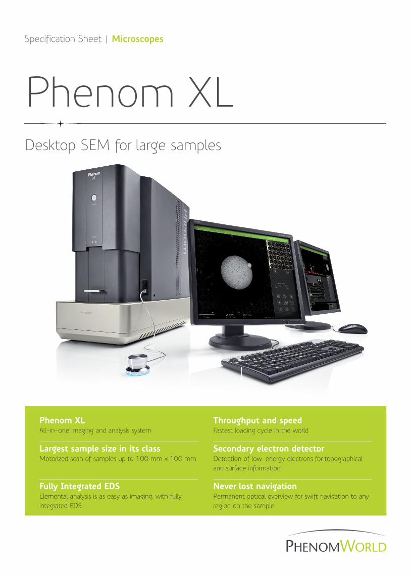
Phenom XLAll-in-one imaging and analysis system
Largest sample size in its classMotorized scan of samples up to 100 mm x 100 mm
Fully Integrated EDSElemental analysis is as easy as imaging, with fully integrated EDS
Throughput and speedFastest loading cycle in the world
Secondary electron detector Detection of low-energy electrons for topographical and surface information
Never lost navigationPermanent optical overview for swift navigation to any region on the sample
Desktop SEM for large samples
Phenom XL

Imaging Specifications
Phenom XL
Specification sheet | Phenom XL02
The Phenom XL Scanning Electron Microscope (SEM) pushes the boundaries of compact desktop SEM performance. It features the proven ease-of-use and fast time-to-image of any Phenom system. It is also equipped with a chamber that allows analysis of large samples up to 100 mm x 100 mm. A proprietary venting/loading mechanism ensures the fastest vent/load cycle in the world, providing the highest throughput. A newly developed compact motorized stage enables the user to scan the full sample area, and yet the Phenom XL is a desktop SEM that needs little space and no extra facilities. Ease-of-use is given an extra boost in the Phenom XL with a single-shot optical navigation camera that allows the user to move to any spot on the sample with just a single click – within seconds.
The Phenom XL features a newly designed chamber including a compact motorized stage that allows analysis of samples of up to 100 mm x 100 mm. In spite of this much larger sample size, a proprietary loading shuttle keeps the vent/load cycle to a minimum, which in practice enables a throughput that is a few factors higher than any comparable SEM system. The user interface is based on the proven ease-of-use technology already applied in the successful Phenom Pro and ProX desktop SEM. The interface enables both existing and new users to quickly become familiar with the system without much training. The standard
detector in the Phenom XL is a four-segment BackScatter Detector (BSD) that yields sharp images and provides chemical contrast information. The Phenom XL can be equipped with two optional detector systems. The first one is a fully integrated EDS system for elemental analysis. The second option is a Secondary Electron Detector (SED) that enables surface sensitive imaging. The ProSuite software application platform is also available for the Phenom XL. With the ProSuite software, and applications such as ParticleMetric, PoroMetric, FiberMetric and 3D Roughness Reconstruction the user can further analyze samples.
Imaging modes> Light optical Magnification range: 3 - 16x> Electron optical Magnification range: 80 - 100,000x Digital zoom max. 12x
Illumination detector> Light optical Bright field / dark field modes> Electron optical Long-lifetime thermionic source (CeB6) Multiple beam currents> Acceleration voltages Default: 5 kV, 10 kV and 15 kV Advanced mode: adjustable range between 4,8 kV and 15 kV imaging and analysis mode Secondary Electron Detector > Resolution ≤ 20 nm
Detector> Standard BackScatter Detector> Optional Secondary Electron Detector
Digital image detection> Light optical Proprietary high-resolution color navigation camera, single shot> Electron optical High-sensitivity BackScatter Detector (compositional and topographical modes)Image formats JPEG, TIFF, BMPImage resolutation options 456 x 456, 684 x 684, 1024 x 1024
and 2048 x 2048 pixelsData storage USB flash drive Network ProSuite PCSample Stage Computer-controlled motorized X and YSample size Max. 100 mm x 100 mm (up to 36 x 12 mm pin stubs) Max. 65 mm (h)Scan area 50 mm x 50 mm 100 mm x 100 mm (optional)Sample loading time> Optical < 5 s> From optical to SEM < 60 s

EDS Specifications System Specifications
Specification sheet | Phenom XL 03
Detector type Silicon Drift Detector (SDD) Thermoelectrically cooled (LN2 free)> Detector active Area 25 mm2
> X-ray window Ultra-thin Silicon Nitride (Si3N4) window allowing detection of elements B to Am
> Energy resolution Mn Kα ≤ 137 eV> Processing capabilities Multi-channel analyzer with 2048
channels at 10 eV/ch> Max. input count rate 300,000 cps > Hardware integration Fully embedded
Software Integrated in Phenom ProSuite Integrated column and stage control Auto-peak ID Iterative strip peak deconvolution Confidence of analysis indicator Export functions: CSV, JPG, TIFF,
ELID, EMSA
Report Docx format
Dimensions & Weight> Imaging module 316(w) x 587(d) x 625(h) mm, 75 kg> Diaphragm vacuum pump 145(w) x 220(d) x 213(h) mm, 4.5 kg> Power supply 156(w) x 300(d) x 74(h) mm, 3 kg> Monitor 375(w) x 203(d) x 395(h) mm, 7.9 kg> ProSuite Standard ProSuite System including: 19” monitor with PC and network
router mounted 375(w) x 250(d) x 395(h) mm, 9 kg
RequirementsAmbient conditions> Temperature 15°C ~ 30°C (59°F ~ 86°F)> Humidity < 80% RH> Power Single phase AC 110 - 240 Volt,
50/60 Hz, 300 W (max.)
Recommended table size 150 x 75 cm, load rating of 100 kg
Step-by-step data collection
Elemental analysis can be added by EDS technology already proven on the Phenom ProX. Energy Dispersive Spectroscopy (EDS) allows users to analyze the chemical composition of their samples. Detailed chemical composition can be obtained from a micro volume via a spot analysis. Elemental distribution can be visualized with the elemental mapping option. An optional Secondary Electron Detector (SED) is available for applications that require surface and topography sensitive imaging.
The dedicated software package Element Identification (EID) isused to control the fully integrated EDS detector. Analysis hasbecome as easy as imaging, since there is no need to switchbetween external software packages or computers. The CeB6 electron source in the Phenom is used to generate the highest X-ray count rate in its market segment, allowing fast results. The EID software package allows the user to identify nearly all materials in the periodic table, starting from Boron (5) and ranging up to Americium (95). It is a perfect analysis tool for a wide range of samples and applications.
Projects can be stored locally or on the network, where theycan be analyzed at a later stage or offline.The EID software package runs smart algorithms with advanced peak analysis to optimize the auto-identification functionality, while still allowing for manual adjustments by the user at any time in the analysis process.The intuitive step-by-step process within the software helpsthe user to collect all X-ray results in an organized and structured way
Phenom-World BV, Dillenburgstraat 9E, 5652 AM Eindhoven, The Netherlands, www.phenom-world.com©2015. Specifications and prices are subject to change without notice. All rights reserved. Reproduction, copying, usage,modifying, hiring, renting, public performance, transmission and/or broadcasting in whole or in part is prohibited withoutthe written consent of Phenom-World BV. Find your Phenom-World contact information at www.phenom-world.com
Elemental Mapping & Line Scan Specifications SED Specifications
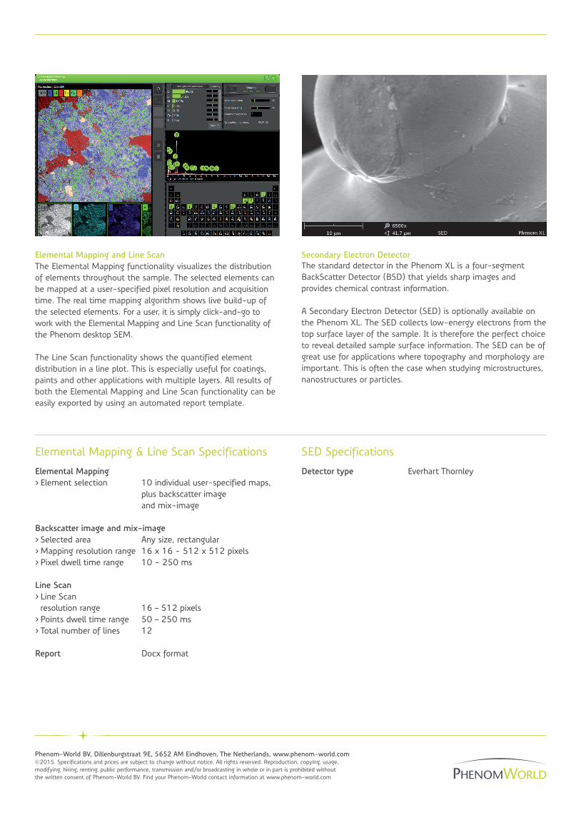
Elemental Mapping and Line Scan Secondary Electron Detector
Elemental Mapping> Element selection 10 individual user-specified maps, plus backscatter image and mix-image
Backscatter image and mix-image> Selected area Any size, rectangular> Mapping resolution range 16 x 16 - 512 x 512 pixels> Pixel dwell time range 10 - 250 ms
Line Scan> Line Scan resolution range 16 – 512 pixels> Points dwell time range 50 – 250 ms> Total number of lines 12
Report Docx format
Detector type Everhart Thornley
The Elemental Mapping functionality visualizes the distributionof elements throughout the sample. The selected elements canbe mapped at a user-specified pixel resolution and acquisitiontime. The real time mapping algorithm shows live build-up ofthe selected elements. For a user, it is simply click-and-go to work with the Elemental Mapping and Line Scan functionality of the Phenom desktop SEM.
The Line Scan functionality shows the quantified element distribution in a line plot. This is especially useful for coatings, paints and other applications with multiple layers. All results of both the Elemental Mapping and Line Scan functionality can be easily exported by using an automated report template.
The standard detector in the Phenom XL is a four-segmentBackScatter Detector (BSD) that yields sharp images andprovides chemical contrast information.
A Secondary Electron Detector (SED) is optionally available on the Phenom XL. The SED collects low-energy electrons from the top surface layer of the sample. It is therefore the perfect choice to reveal detailed sample surface information. The SED can be of great use for applications where topography and morphology are important. This is often the case when studying microstructures, nanostructures or particles.