nanofabrication2008 lecture 6 lg - aau
TRANSCRIPT

Lecture 6
Photoresist

Simple exposure system
Last lecture
Today’s lectureformation of an areal image
registration of an areal image in a photosensitive layer

Lecture content
• Resist chemistry• Resist resolution and line profile• Resist technology• Advanced resists

Resolution of the aerial image
( )W k z gλ≈ +~1 distance
wavelength
Contact/proximity
minW kNAλ
≈
~1 – 0.3
• k depends on many factors incl. illumination system, mask etc.

Photoresists• Resist polarity
– positive resists: exposed regions dissolve in the developer
– negative resist: unexposed regions dissolve
better resolution,commonly used
desired qualities: sensitivity (mJ/cm2)resolution
photoresist = resin (base material) + photoactive component (PAC) + solvent

Mechanism of a simple photoresist• Solubility of a polymer ~ MW-2.
– so, scission of a polymer during exposure leads to better solubility: positive resist, e.g. PMMA, ZEP
Poly(methylmethacrylate) - PMMA resist
– cross-linking of a polymer during exposure leads to reduced solubility: negative photoresist, e.g. Polystyrene
poly(methyl-a-chloroacrylate-co- a-methylstyrene)
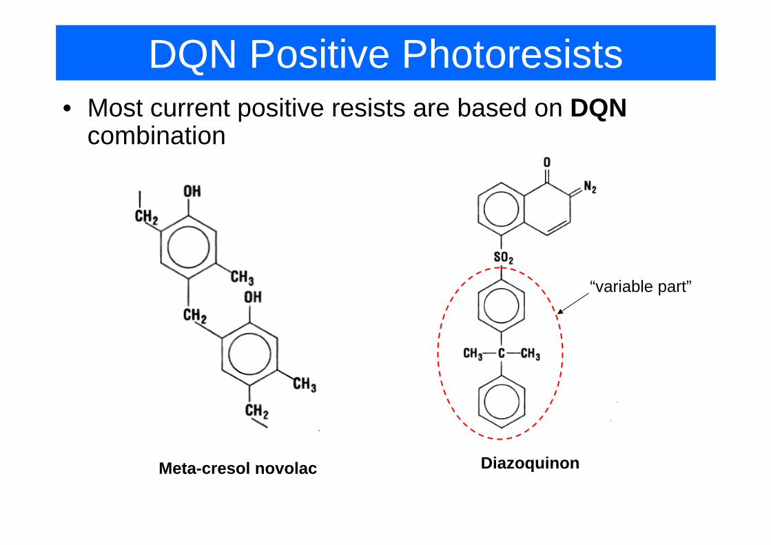
DQN Positive Photoresists• Most current positive resists are based on DQN
combination
Meta-cresol novolac Diazoquinon
“variable part”

DQN Positive Photoresists
• Novolac: – viscous liquid, viscosity can be
adjusted with organic solvents;– dissolves easily in aqueous
solutions
Meta-cresol novolac

DQN Positive PhotoresistsDiazoquinon• in unexposed state acts as
inhibitor, reduces dissolution rate in developer by factor >10(softbake crucial!)
• in exposed state helps dissolution in developer
Diazoquinon

DQN Positive Photoresists• Photolysis of DQ
foams resist, assist dissolution
carboxylic acid, dissolves in base solution

DQN Positive Photoresists
• Advantages:– unexposed areas are not attacked by the
developer: possible to create narrow lines on a blank field
– fairly resistant to chemical attack (incl. plasma etching)
• Example: Shipley S1800 family of resists

Negative resists
• usually employ crosslinking: larger molecules are less soluble
• high photo speed• main disadvantage: swelling during
development in organic solvents• generally not used for features smaller than
2um

Contrast curves and Resolution
• Slope of photoresistlines:
dZ dZ dDdX dD dX
⎛ ⎞⎛ ⎞= ⎜ ⎟⎜ ⎟⎝ ⎠⎝ ⎠
profile vs. dose,i.e. contrast
dose vs. coordinate,i.e. aerial image

Contrast curves and Resolution• contrast curves for idealized positive and negative tone resists
100 0
1log( / )D D
γ =the contrast
energy dosefor 100% removal
energy dosefor to start ph/chem
The measure of the ability of a resist to distinguish between black and white areas of the mask :

Contrast curves and Resolution
• contrast values for common resists
2.13.63.643623.63.63651.93.43.43130.850.70.7248
Hunt 204AZ-1450AZ-1350l (nm)
• typical contrast 2-5, i.e.1152
100 0 10 10D D = −
• contrast depends on the processing e.g. softbake, postbake, wavelength, development etc.

Contrast curves and Resolution• calculating the resist profile
resist profile at several exposure times
dZ dZ dDdX dD dX
⎛ ⎞⎛ ⎞= ⎜ ⎟⎜ ⎟⎝ ⎠⎝ ⎠
• lower exposures (< 50mJ/cm2):shallow angle resist profile
• high exposure (>150mJ/cm2):sharp profile determined by the quality of aerial image and scattering
• typically exposure is in moderate or high exposure regimes
x time =dose

Contrast curves and Resolution• light absorption in the resist
0zI I e α−=
• D0 – independent on the resist thickness (TR)• D100 – inversely proportional to adsorbance A:
0
0
( ( ))11
R
R
T
T
R R
I I z dzeA
I I T
α
α
−−
−= = −∫
• the contrast is 1
RTγ
β α=
+
! thinner resist has higher contrast though less stable against etch and might limit the thickness of lift-off layer.
contrast drops with the resist thickness!

Contrast curves and Resolution• The Critical Modulation Transfer Function (CMTF)
100 0
100 0resist
D DCMTFD D
−=
+
• The resolution criterion:For successfully resolved image the MTF should be larger than CMTF
1/
1/
10 110 1resistCMTF
γ
γ
−=
+
( ) 1100 0log( / )D Dγ −=

Radiation and Resist profiles
• scattering at the resist interface and adsorption affect the resist profile
wet etch<5dominantlow
dry etch, lift-off, wet etch
5-10moderatemoderate
lift-off, ion implant
>10lowhigh
UsesR/R0Developer influence
DoseProfile
develop rate for exposed/unexposed resist

Resist technologyDehydrate bake
Adhesion promoter application
Resist application
Softbake
Exposure
Post exposure bake
Develop cycle
Hardbake
Resist stabilization
150 – 200 oC in vacuum or dry nitrogen
usually, HMDS (hexamethyldisilazane)via spin coating or vapour depositionspin coating with static or dynamic dispenseto remove solvent and establish exposure characteristics, typ. 90-100 oC
required for some (negative) resists
alkaline develop for DQN (or alkaline-free based on TMAH (tetramethyl ammonium hydroxide)
to increase resist stability for etching
1RT ω∝

Resist technology• spin coating – critical process!
depends on: – deposition technique (static, dynamic, prespin)– acceleration (important for uniformity)– spin rate (2000 – 6000 rpm)– resist viscosity
1RT
ω∝
Spin curves for Shipley S1800

Resist technology• spin coating – equipment:
– automated track systems: high reproducibility, high costs
– manual spin coater + hot plate/oven

Resist technology• Develop – can change the image contrast
single spray puddle
double spray puddle
techniques• tank• puddle• spray etc.Developer• metal bearing • metal free

Resist technology• hardbake – changes
chemical/physical properties, affects the pattern
• resist profiles of 1 mm line vs. hardbake T

Second-order exposure effects• absorption in the resist and absorption spectrum• actinic effect (bleaching)
transparency of exposed resist increasing
• effect of the underlying topography: thickness variation will cause line width variation.
thinthick

Advanced Photoresists• Resist for 193 nm and 157 nm lines
– Novolac strongly adsorbs below 248 nm and DQ doesn’t bleach significantly
– Possibilities:• Chemically amplified resist (CAR) system based
on DQN. Typically: Photoacid generator (PAG)• PMMA or other polymers that undergo chain
scission or crosslinking. (high contrast, but low sensitivity ~200 mJ/cm2, against 5-10 mJ/cm2
required, very low etch resistance).• acrylic-based resins with PAG and a protection
agent

Advanced Photoresists
• CAR related effects:– diffusion of PAG from exposed to unexposed
regions– deterioration of the surface of the resist upon
exposure to air

Advanced Photoresists
• Inorganic resists
• Ag/Se-Ge:– very high contrast g~7– requires planarization– tends to have pinholes– defects added during
plating

Advanced Photoresists
• dry developable resists
Example: Si-containing resists (polysilynes-based)

Multilayer resist• multilayer resist may be required for
– resolution improvement– topography planarization– lift-off improvement – etching improvement etc.

Gray-scale lithography• regime where resist profile strongly depends on exposure (low doses) can be used
to create 3D structures
SU8 gray scale lithography
fabrication of aspherical lens array by gray scale lithography
DMD superposition of an image stack photoresist pattern pattern in silicon
dryetch

Shipley S1800 resist • positive resist• exist in a number of different
viscosity formulation, we use S1813

SU8-2000• negative resist, • thick layers <200mm in a single coat• high aspect ratios, up to 1:10 • vertical sidewalls

SU-8 2000 (cont)
• soft bake
• spin coat
• exposure
• postbake

Problems• 8.1: Calculate CMTF for AZ-1450 at the
wavelengths listed in the table. Assuming NA=0.4 use figure 7.22 to determine the minimum feature for an aligner with S=0.5.
3.64363.63653.43130.7248
Contrast AZ-1450
l (nm)
• 8.15: Assume that a wafer is being exposed with a proximity printer. In the far field limit in one dimension intensity depends as:
• Assume that you are using 1 µm thick positive tone resist with D0=30mJ/cm2 and D100=100mJ/cm2. For l=436nm, g=10µm, and I(0)=100mW.µm2/cm2 calculate resist profiles for W=1µm and exposure times 1, 2, 4, and 7 sec.
222 2 2( ) (0) ; sinx x
W xW xWI x I I Ig gg
π πλ λλ
⎡ ⎤ ⎡ ⎤= =⎢ ⎥ ⎢ ⎥
⎣ ⎦⎣ ⎦

ProblemsProblem 8.1