pcn product/process change notification - anglia · pcn product/process change notification ......
TRANSCRIPT
STMicroelectronics ADG - ASD & IPAD™ Division1 BU Protection
(1) ADG: Automotive and Discretes Group - ASD: Application Specific Device – IPAD™: Integrated Passive and Active Devices
Issue date 24-01-2017 1/2
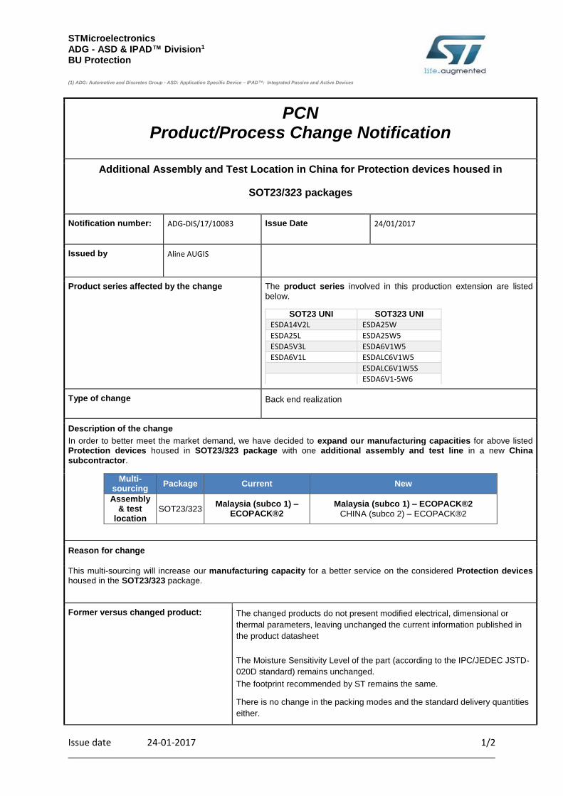
PCN Product/Process Change Notification
Additional Assembly and Test Location in China for Protection devices housed in
SOT23/323 packages
Notification number: ADG-DIS/17/10083 Issue Date 24/01/2017
Issued by Aline AUGIS
Product series affected by the change
The product series involved in this production extension are listed
below.
SOT23 UNI SOT323 UNI
ESDA14V2L ESDA25W
ESDA25L ESDA25W5
ESDA5V3L ESDA6V1W5
ESDA6V1L ESDALC6V1W5
ESDALC6V1W5S
ESDA6V1-5W6
Type of change Back end realization
Description of the change
In order to better meet the market demand, we have decided to expand our manufacturing capacities for above listed Protection devices housed in SOT23/323 package with one additional assembly and test line in a new China subcontractor.
Multi-sourcing
Package Current New
Assembly & test
location SOT23/323
Malaysia (subco 1) – ECOPACK®2
Malaysia (subco 1) – ECOPACK®2
CHINA (subco 2) – ECOPACK®2
Reason for change
This multi-sourcing will increase our manufacturing capacity for a better service on the considered Protection devices housed in the SOT23/323 package.
Former versus changed product: The changed products do not present modified electrical, dimensional or
thermal parameters, leaving unchanged the current information published in
the product datasheet
The Moisture Sensitivity Level of the part (according to the IPC/JEDEC JSTD-
020D standard) remains unchanged.
The footprint recommended by ST remains the same.
There is no change in the packing modes and the standard delivery quantities
either.

STMicroelectronics ADG - ASD & IPAD™ Division1 BU Protection
(1) ADG: Automotive and Discretes Group - ASD: Application Specific Device – IPAD™: Integrated Passive and Active Devices
Issue date 24-01-2017 2/2
The products remain in full compliance with the ST ECOPACK®2 grade
(“halogen-free”).
Disposition of former products
Deliveries of former product will continue.
Marking and traceability
Traceability for the implemented change will be ensured by internal codification and by the Q.A. number.
Qualification complete date 06-01-2016
Forecasted sample availability
Samples are available upon request.
Change implementation schedule
Sales types Estimated production start Estimated first shipments
All Week 12-2017 Week 17-2017
Comments:
Customer’s feedback
Please contact your local ST sales representative or quality contact for requests concerning this change notification.
Absence of acknowledgement of this PCN within 30 days of receipt will constitute acceptance of the change
Absence of additional response within 90 days of receipt of this PCN will constitute acceptance of the change
Qualification program and results 17001QRP-Rev1.0
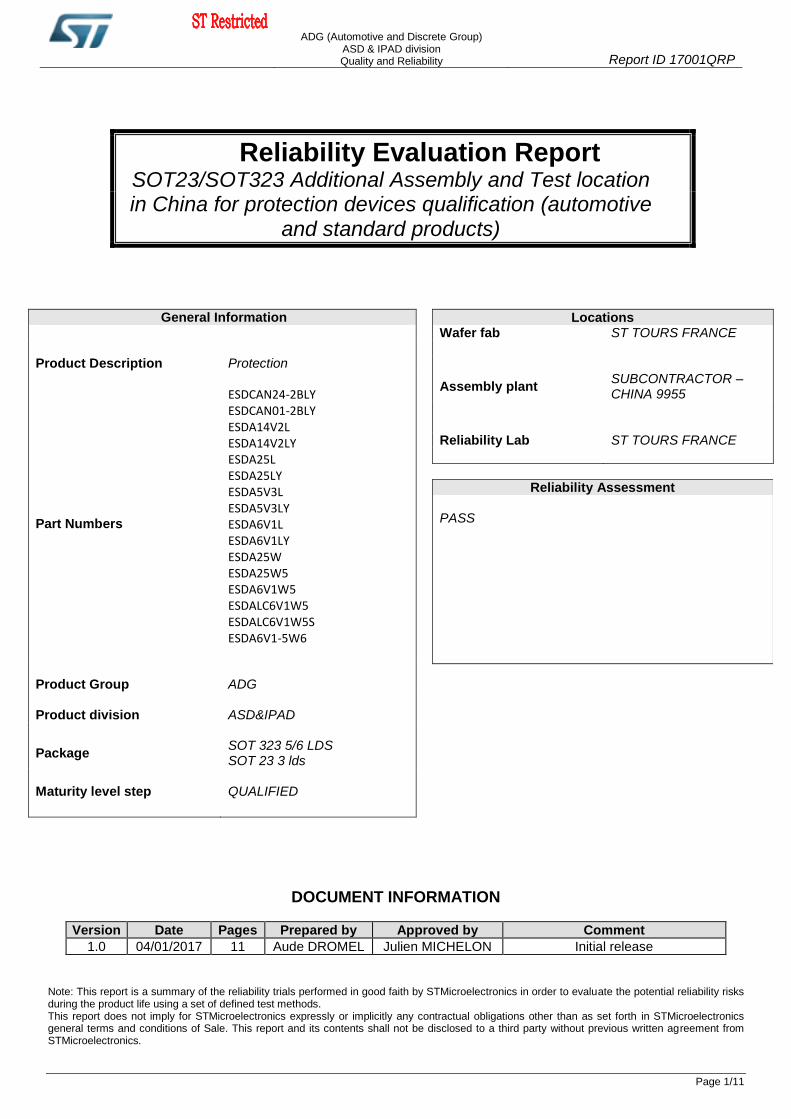
ADG (Automotive and Discrete Group)
ASD & IPAD division Quality and Reliability Report ID 17001QRP
Page 1/11
Reliability Evaluation Report SOT23/SOT323 Additional Assembly and Test location in China for protection devices qualification (automotive
and standard products)
General Information Product Description
Protection
Part Numbers
ESDCAN24-2BLY ESDCAN01-2BLY ESDA14V2L ESDA14V2LY ESDA25L ESDA25LY ESDA5V3L ESDA5V3LY ESDA6V1L ESDA6V1LY ESDA25W ESDA25W5 ESDA6V1W5 ESDALC6V1W5 ESDALC6V1W5S ESDA6V1-5W6
Product Group
ADG
Product division
ASD&IPAD
Package
SOT 323 5/6 LDS SOT 23 3 lds
Maturity level step
QUALIFIED
Locations Wafer fab ST TOURS FRANCE
Assembly plant SUBCONTRACTOR – CHINA 9955
Reliability Lab ST TOURS FRANCE
Reliability Assessment PASS
DOCUMENT INFORMATION
Version Date Pages Prepared by Approved by Comment
1.0 04/01/2017 11 Aude DROMEL Julien MICHELON Initial release
Note: This report is a summary of the reliability trials performed in good faith by STMicroelectronics in order to evaluate the potential reliability risks during the product life using a set of defined test methods. This report does not imply for STMicroelectronics expressly or implicitly any contractual obligations other than as set forth in STMicroelectronics general terms and conditions of Sale. This report and its contents shall not be disclosed to a third party without previous written agreement from STMicroelectronics.

ADG (Automotive and Discrete Group)
ASD & IPAD division Quality and Reliability Report ID 17001QRP
Page 2/11
TABLE OF CONTENTS
1 APPLICABLE AND REFERENCE DOCUMENTS ........................................................................................... 3 2 GLOSSARY ....................................................................................................................................................... 3 3 RELIABILITY EVALUATION OVERVIEW ........................................................................................................ 4
3.1 OBJECTIVES .............................................................................................................................................. 4 3.2 CONCLUSION ............................................................................................................................................. 4
4 DEVICE CHARACTERISTICS .......................................................................................................................... 5 4.1 DEVICE DESCRIPTION ................................................................................................................................. 5 4.2 CONSTRUCTION NOTE ................................................................................................................................ 5
5 TESTS RESULTS SUMMARY .......................................................................................................................... 7 5.1 TEST VEHICLES .......................................................................................................................................... 7 5.2 TEST PLAN AND RESULTS SUMMARY ............................................................................................................ 7
6 ANNEXES ........................................................................................................................................................ 10 6.1 TESTS DESCRIPTION ................................................................................................................................ 10
ADG (Automotive and Discrete Group)
ASD & IPAD division Quality and Reliability Report ID 17001QRP
Page 3/11
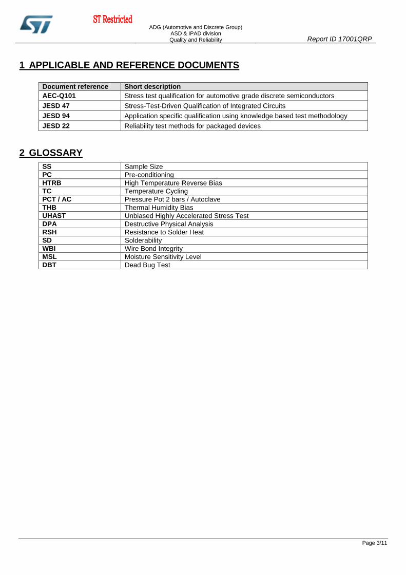
1 APPLICABLE AND REFERENCE DOCUMENTS
Document reference Short description
AEC-Q101 Stress test qualification for automotive grade discrete semiconductors
JESD 47 Stress-Test-Driven Qualification of Integrated Circuits
JESD 94 Application specific qualification using knowledge based test methodology
JESD 22 Reliability test methods for packaged devices
2 GLOSSARY
SS Sample Size
PC Pre-conditioning
HTRB High Temperature Reverse Bias
TC Temperature Cycling
PCT / AC Pressure Pot 2 bars / Autoclave
THB Thermal Humidity Bias
UHAST Unbiased Highly Accelerated Stress Test
DPA Destructive Physical Analysis
RSH Resistance to Solder Heat
SD Solderability
WBI Wire Bond Integrity
MSL Moisture Sensitivity Level
DBT Dead Bug Test
ADG (Automotive and Discrete Group)
ASD & IPAD division Quality and Reliability Report ID 17001QRP
Page 4/11
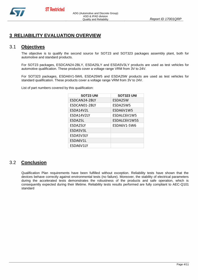
3 RELIABILITY EVALUATION OVERVIEW
3.1 Objectives
The objective is to qualify the second source for SOT23 and SOT323 packages assembly plant, both for automotive and standard products. For SOT23 packages, ESDCAN24-2BLY, ESDA25LY and ESDA5V3LY products are used as test vehicles for automotive qualification. These products cover a voltage range VRM from 3V to 24V. For SOT323 packages, ESDA6V1-5W6, ESDA25W5 and ESDA25W products are used as test vehicles for standard qualification. These products cover a voltage range VRM from 3V to 24V. List of part numbers covered by this qualification:
SOT23 UNI SOT323 UNI
ESDCAN24-2BLY ESDA25W ESDCAN01-2BLY ESDA25W5 ESDA14V2L ESDA6V1W5 ESDA14V2LY ESDALC6V1W5 ESDA25L ESDALC6V1W5S ESDA25LY ESDA6V1-5W6 ESDA5V3L
ESDA5V3LY
ESDA6V1L
ESDA6V1LY
3.2 Conclusion
Qualification Plan requirements have been fulfilled without exception. Reliability tests have shown that the devices behave correctly against environmental tests (no failure). Moreover, the stability of electrical parameters during the accelerated tests demonstrates the robustness of the products and safe operation, which is consequently expected during their lifetime. Reliability tests results performed are fully compliant to AEC-Q101 standard

ADG (Automotive and Discrete Group)
ASD & IPAD division Quality and Reliability Report ID 17001QRP
Page 5/11
4 DEVICE CHARACTERISTICS
4.1 Device description
See referenced Datasheet document.
Pin connection
4.2 Construction note
ESDCAN242BLY, ESDA5V3LY, ESDA25LY
Wafer/Die fab. information
Wafer fab manufacturing location ST TOURS GLOBAL 6"
Technology / Process family ASD-TRANSIL
Wafer Testing (EWS) information
Electrical testing manufacturing location ST TOURS
Assembly information
Assembly site SUBCONTRACTOR. - CHINA
Package description SOT 23 3LDS
Final testing information
Testing location SUBCONTRACTOR. - CHINA
ADG (Automotive and Discrete Group)
ASD & IPAD division Quality and Reliability Report ID 17001QRP
Page 6/11
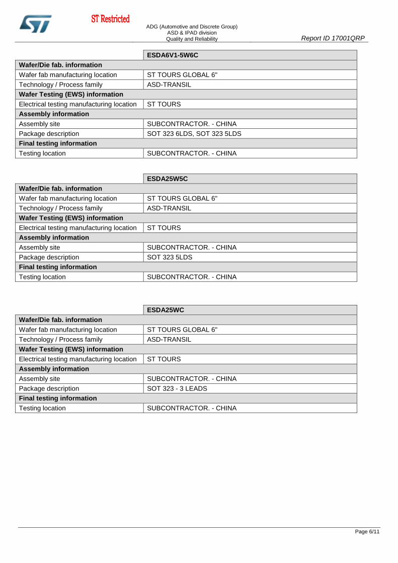
ESDA6V1-5W6C
Wafer/Die fab. information
Wafer fab manufacturing location ST TOURS GLOBAL 6"
Technology / Process family ASD-TRANSIL
Wafer Testing (EWS) information
Electrical testing manufacturing location ST TOURS
Assembly information
Assembly site SUBCONTRACTOR. - CHINA
Package description SOT 323 6LDS, SOT 323 5LDS
Final testing information
Testing location SUBCONTRACTOR. - CHINA
ESDA25W5C
Wafer/Die fab. information
Wafer fab manufacturing location ST TOURS GLOBAL 6"
Technology / Process family ASD-TRANSIL
Wafer Testing (EWS) information
Electrical testing manufacturing location ST TOURS
Assembly information
Assembly site SUBCONTRACTOR. - CHINA
Package description SOT 323 5LDS
Final testing information
Testing location SUBCONTRACTOR. - CHINA
ESDA25WC
Wafer/Die fab. information
Wafer fab manufacturing location ST TOURS GLOBAL 6"
Technology / Process family ASD-TRANSIL
Wafer Testing (EWS) information
Electrical testing manufacturing location ST TOURS
Assembly information
Assembly site SUBCONTRACTOR. - CHINA
Package description SOT 323 - 3 LEADS
Final testing information
Testing location SUBCONTRACTOR. - CHINA
ADG (Automotive and Discrete Group)
ASD & IPAD division Quality and Reliability Report ID 17001QRP
Page 7/11
5 TESTS RESULTS SUMMARY
5.1 Test vehicles
Lot # Part Number Die
manufacturing plant
Package Assembly plant Comments
Lot 1 ESDA6V1-5W6
ST TOURS FRANCE
SOT 323 6 LDS
SUBCONTRACTOR CHINA
Qualification lots SOT323 Lot 2 ESDA25W5 SOT 323 5 LDS
Lot 3 ESDA25W SOT 323
Lot 4 ESDCAN24-2BLY
SOT 23 3 LDS Qualification lots SOT23
auto
Lot 5 ESDA5V3LY
Lot 6 ESDA25LY
Lot 7 ESDCAN24-2BLY
Lot 8 ESDCAN01-2BLY
Lot 9 ESDCAN24-2BLY
Lot 10 ESDCAN24-2BLY
Detailed results in below chapter will refer to P/N and Lot #.
5.2 Test plan and results summary
5.2.1 Standard products
Test PC Std ref. Conditions SS Steps
Failure/SS
Lot 1 Lot 2 Lot 3
HTRB N JESD22 A-108 Junction
Temperature=125°C Tension=3V
75
168h 0/75 - -
504h 0/75 - -
1000h 0/75 - -
HTRB
N JESD22 A-108 Junction
Temperature=125°C Tension=24V
154
168h - 0/77 0/77
504h - 0/77 0/77
1000h - 0/77 0/77
TC Y JESD22 A-104
Frequency (cy/h)=2cy/h Temperature (high)=150°C Temperature (low)=-65°C
74 500cy 0/74 - -
THB Y JESD22 A-101 Humidity (HR)=85% Temperature=85°C
Tension=3V 77
168h 0/77 - -
504h 0/77 - -
1000h 0/77 - -
SD N JESD22 B-102
Steam Ageing SnAgCu bath 245°C
60
visual inspection
0/15 - -
Steam Ageing SnPb 220°C
visual inspection
0/15 - -
Dry Ageing SnAgCu 245°C
visual inspection
0/15 - -
Dry Ageing SnPb 220°C
visual inspection
0/15 - -
MSL research
Y JESD22 A-113 Humidity (HR)=85%
MSL=1 Temperature=85°C
30 168h 0/30 - -
ADG (Automotive and Discrete Group)
ASD & IPAD division Quality and Reliability Report ID 17001QRP
Page 8/11
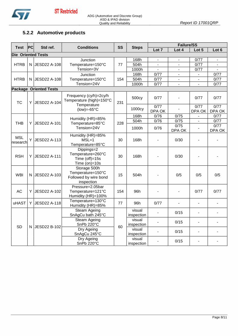
5.2.2 Automotive products
Test PC Std ref. Conditions SS Steps Failure/SS
Lot 7 Lot 4 Lot 5 Lot 6
Die Oriented Tests
HTRB N JESD22 A-108 Junction
Temperature=150°C Tension=3V
77
168h - - 0/77 -
504h - - 0/77 -
1000h - - 0/77 -
HTRB N JESD22 A-108 Junction
Temperature=150°C Tension=24V
154
168h 0/77 - - 0/77
504h 0/77 - - 0/77
1000h 0/77 - - 0/77
Package Oriented Tests
TC Y JESD22 A-104
Frequency (cy/h)=2cy/h Temperature (high)=150°C
Temperature (low)=-65°C
231
500cy 0/77 - 0/77 0/77
1000cy 0/77
DPA OK -
0/77 DPA OK
0/77 DPA OK
THB Y JESD22 A-101 Humidity (HR)=85% Temperature=85°C
Tension=24V 228
168h 0/76 0/75 - 0/77
504h 0/76 0/75 - 0/77
1000h 0/76 0/75
DPA OK -
0/77 DPA OK
MSL research
Y JESD22 A-113 Humidity (HR)=85%
MSL=1 Temperature=85°C
30 168h - 0/30 - -
RSH Y JESD22 A-111
Dippings=2 Temperature=260°C
Time (off)=15s Time (on)=10s
30 168h - 0/30 - -
WBI N JESD22 A-103
Storage 500h Temperature=150°C
Followed by wire bond inspection
15 504h - 0/5 0/5 0/5
AC Y JESD22 A-102 Pressure=2.05bar
Temperature=121°C Humidity (HR)=100%
154 96h - - 0/77 0/77
uHAST Y JESD22 A-118 Temperature=130°C Humidity (HR)=85%
77 96h 0/77 - - -
SD N JESD22 B-102
Steam Ageing SnAgCu bath 245°C
60
visual inspection
- 0/15 - -
Steam Ageing SnPb 220°C
visual inspection
- 0/15 - -
Dry Ageing SnAgCu 245°C
visual inspection
- 0/15 - -
Dry Ageing SnPb 220°C
visual inspection
- 0/15 - -
ADG (Automotive and Discrete Group)
ASD & IPAD division Quality and Reliability Report ID 17001QRP
Page 9/11
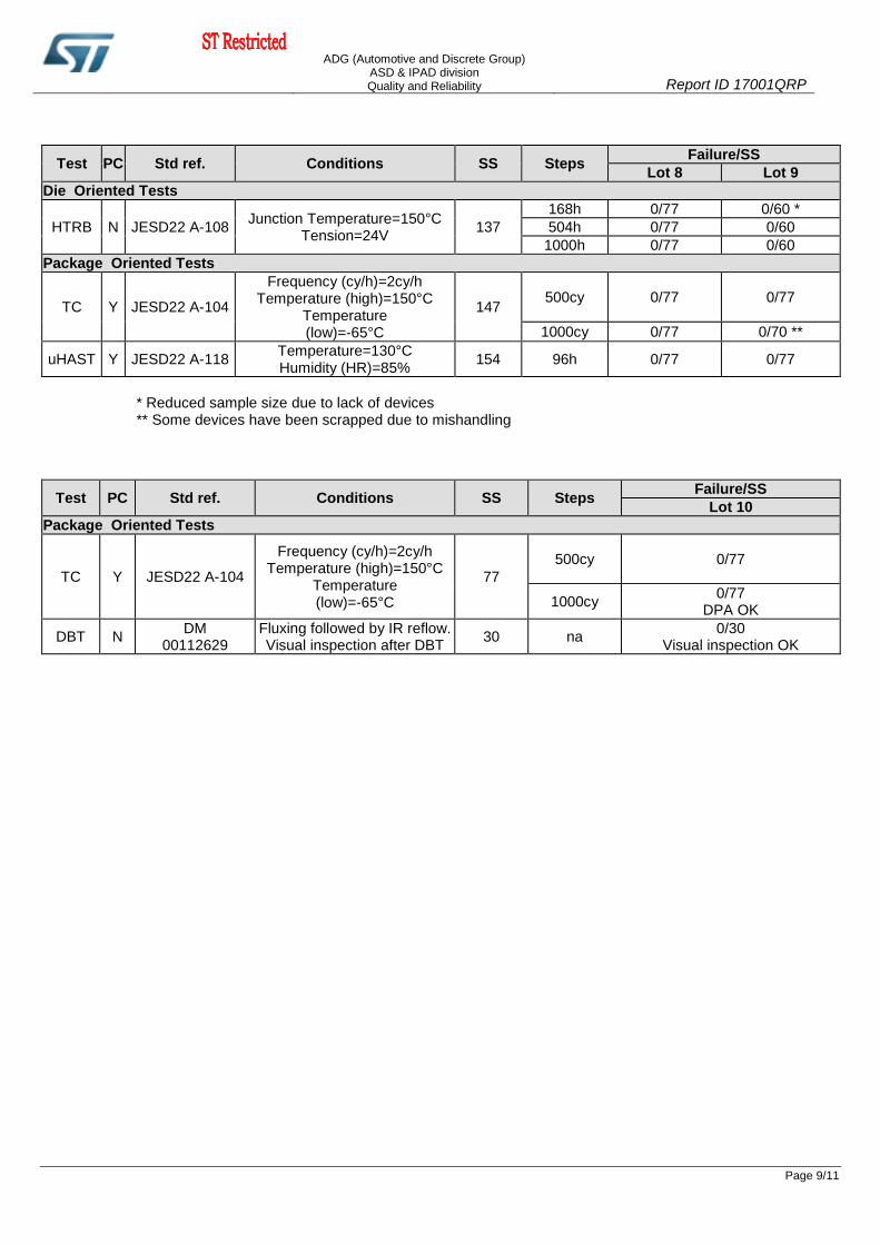
Test PC Std ref. Conditions SS Steps Failure/SS
Lot 8 Lot 9
Die Oriented Tests
HTRB N JESD22 A-108 Junction Temperature=150°C
Tension=24V 137
168h 0/77 0/60 *
504h 0/77 0/60
1000h 0/77 0/60
Package Oriented Tests
TC Y JESD22 A-104
Frequency (cy/h)=2cy/h Temperature (high)=150°C
Temperature (low)=-65°C
147 500cy 0/77 0/77
1000cy 0/77 0/70 **
uHAST Y JESD22 A-118 Temperature=130°C Humidity (HR)=85%
154 96h 0/77 0/77
* Reduced sample size due to lack of devices ** Some devices have been scrapped due to mishandling
Test PC Std ref. Conditions SS Steps Failure/SS
Lot 10
Package Oriented Tests
TC Y JESD22 A-104
Frequency (cy/h)=2cy/h Temperature (high)=150°C
Temperature (low)=-65°C
77
500cy 0/77
1000cy 0/77
DPA OK
DBT N DM
00112629 Fluxing followed by IR reflow. Visual inspection after DBT
30 na 0/30
Visual inspection OK

ADG (Automotive and Discrete Group)
ASD & IPAD division Quality and Reliability Report ID 17001QRP
Page 10/11
6 ANNEXES
6.1 Tests Description
Test name Standard Reference
Description Purpose
Die Oriented
HTRB High
Temperature Reverse Bias
JESD22 A-108
HTRB : High Temperature Reverse
Bias HTFB / HTGB : High Temperature Forward (Gate) Bias
The device is stressed in static configuration, trying to satisfy as much as possible the following conditions: - low power dissipation; - max. supply
voltage compatible with diffusion process and internal circuitry
limitations.
To determine the effects of bias conditions and temperature on solid state devices over
time. It simulates the devices' operating condition in an accelerated way. To
maximize the electrical field across either reverse-biased junctions or dielectric layers,
in order to investigate the failure modes linked to mobile contamination, oxide
ageing, layout sensitivity to surface effects.
Package Oriented
RSH Resistance to
solder heat
JESD22 A-111
Device is submitted to a dipping in a solder bath at 260°C with a dwell time of 10s. Only for through hole mounted
devices.
This test is used to determine whether solid state devices can withstand the effects of
the temperature to which they will be subjected during soldering of their leads. The heat is conducted through the leads
into the device package from solder heat at the reverse side of the board. This
procedure does not simulate wave soldering or reflow heat exposure on the same side of
the board as the package body.
PC
Preconditioning
JESD22 A-113
The device is submitted to a typical temperature profile used for surface mounting devices, after a controlled
moisture absorption.
As stand-alone test: to investigate the moisture sensitivity level. As preconditioning before other reliability tests: to verify that the surface mounting stress does not impact on the subsequent reliability performance. The typical failure modes are "pop corn" effect and delamination.
TC Temperature
Cycling
JESD22 A-104
The device is submitted to cycled temperature excursions, between a hot and a cold chamber in air atmosphere.
To investigate failure modes related to the thermo-mechanical stress induced by the
different thermal expansion of the materials interacting in the die-package system.
Typical failure modes are linked to metal displacement, dielectric cracking, molding
compound delamination, wire-bonds failure, die-attach layer degradation.

ADG (Automotive and Discrete Group)
ASD & IPAD division Quality and Reliability Report ID 17001QRP
Page 11/11
Test name Standard Reference
Description Purpose
THB Temperature Humidity Bias
JESD22 A-101
The device is biased in static
configuration minimizing its internal power dissipation, and stored at controlled conditions of ambient
temperature and relative humidity.
To evaluate the package moisture resistance with electrical field applied, both electrolytic and galvanic corrosion are put in
evidence.
AC
Autoclave
JESD22 A-
102
The device is stored in saturated
steam, at fixed and controlled conditions of pressure and
temperature.
Purpose: to investigate corrosion
phenomena affecting die or package materials, related to chemical contamination
and package hermeticity. To point out critical water entry paths with consequent electrochemical and galvanic
corrosion.
uHAST
JESD22 A-
118
The Unbiased HAST is performed for the purpose of evaluating the reliability of non-hermetic packaged solidstate devices in humid environments
.
Purpose: to investigate corrosion
phenomena affecting die or package materials, related to chemical contamination
and package hermeticity. To point out critical water entry paths with consequent electrochemical and galvanic
corrosion.
Solderability
J-STD-002
The purpose of this test method is to provide a referee condition for the evaluation of the solderability of terminations (including leads up to 0.125 inch in diameter) that will be assembled using tin lead eutectic solder.
This evaluation is made on the basis of the ability of these terminations to be wetted
and to produce a suitable fillet when coated by tin lead eutectic solder. These
procedures will test whether the packaging materials and processes used during the
manufacturing operations process produce a component that can be successfully
soldered to the next level assembly using tin lead eutectic solder. A preconditioning test
is included in this test method, which degrades the termination finish to provide a
guard band against marginal finish.
WBI
Wire Bond Integrity
MIL-STD-750
Method 2037
The device is stored at maximum rated Tj during 500 hours. Decap and wire
bond inspection after storage.
Purpose: to evaluate the quality of the contact of the wire bonding (dissimilar metals) after high temperature storage.
Migration of IMC is expected.
DBT Dead Bug test
DM 00112629
Leads are covered with soldering flux before being submitted to IR reflow.
Assessment by visual inspection of the leads
To ensure good wettability of the leads
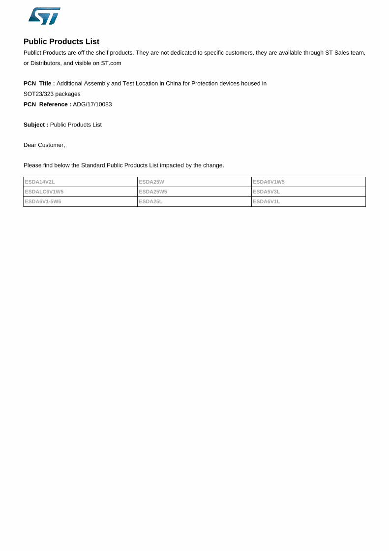
Public Products List
Publict Products are off the shelf products. They are not dedicated to specific customers, they are available through ST Sales team,
or Distributors, and visible on ST.com
PCN Title : Additional Assembly and Test Location in China for Protection devices housed in
SOT23/323 packages
PCN Reference : ADG/17/10083
Subject : Public Products List
Dear Customer,
Please find below the Standard Public Products List impacted by the change.
ESDA14V2L ESDA25W ESDA6V1W5
ESDALC6V1W5 ESDA25W5 ESDA5V3L
ESDA6V1-5W6 ESDA25L ESDA6V1L
Public Products List
IMPORTANT NOTICE – PLEASE READ CAREFULLY
STMicroelectronics NV and its subsidiaries (“ST”) reserve the right to make changes, corrections, enhancements, modifications, and improvements to ST products and/or to this document at any time without notice. Purchasers should obtain the latest relevant information on ST products before placing orders. ST products are sold pursuant to ST’s terms and conditions of sale in place at the time of order acknowledgement.
Purchasers are solely responsible for the choice, selection, and use of ST products and ST assumes no liability for application assistance or the design of Purchasers’ products.
No license, express or implied, to any intellectual property right is granted by ST herein.
Resale of ST products with provisions different from the information set forth herein shall void any warranty granted by ST for such product.
ST and the ST logo are trademarks of ST. All other product or service names are the property of their respective owners.
Information in this document supersedes and replaces information previously supplied in any prior versions of this document.
© 2016 STMicroelectronics – All rights reserved