photonic integrated circuits nasa goddard space … · photonic integrated circuits nasa goddard...
TRANSCRIPT
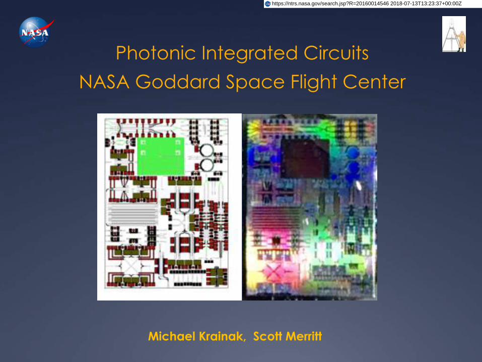
Photonic Integrated Circuits
NASA Goddard Space Flight Center
Michael Krainak, Scott Merritt
https://ntrs.nasa.gov/search.jsp?R=20160014546 2018-07-13T13:23:37+00:00Z

AGENDA
Ü NASA Application Areas for Integrated Photonics
Ü Laser Communication Relay Demonstration (LCRD) modem
Ü Photonic Integrated Circuit (PIC) – Examples
Ü Direct-Write Waveguides, Machining, Patterning, Bonding…
Ü Our Early Stage Innovators
Ü Acknowledgements
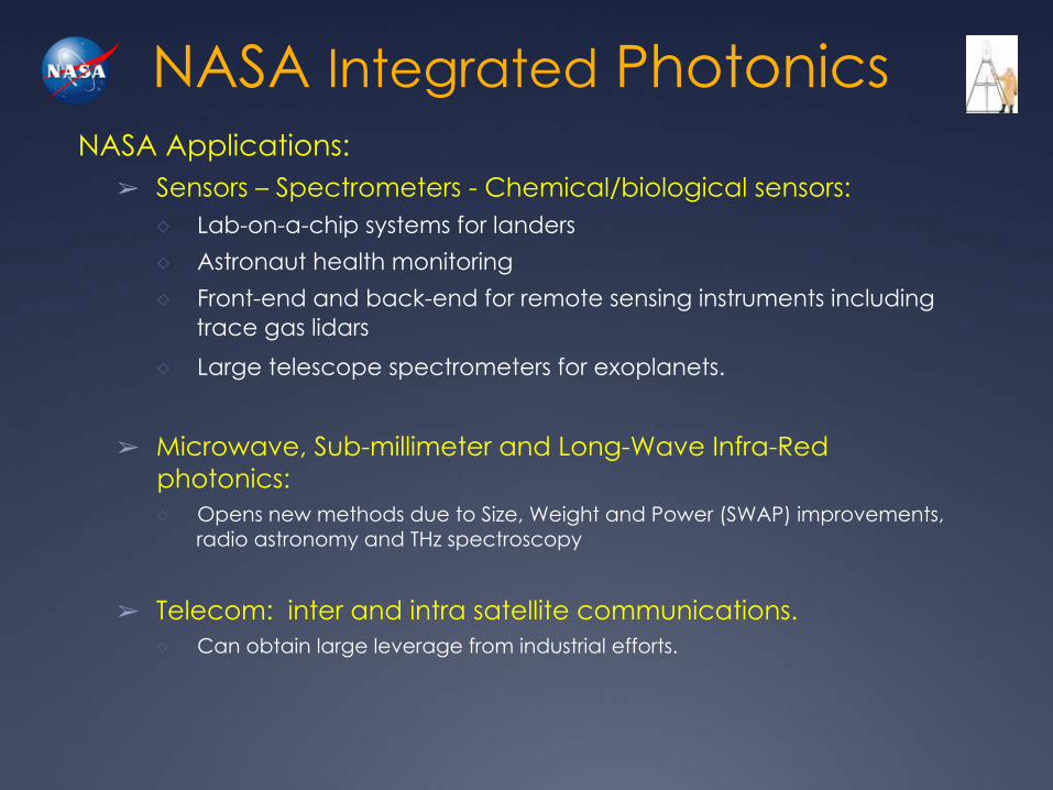
NASA Integrated Photonics NASA Applications:
➢ Sensors – Spectrometers - Chemical/biological sensors: ◇ Lab-on-a-chip systems for landers ◇ Astronaut health monitoring ◇ Front-end and back-end for remote sensing instruments including
trace gas lidars
◇ Large telescope spectrometers for exoplanets.
➢ Microwave, Sub-millimeter and Long-Wave Infra-Red photonics: ◇ Opens new methods due to Size, Weight and Power (SWAP) improvements,
radio astronomy and THz spectroscopy
➢ Telecom: inter and intra satellite communications. ◇ Can obtain large leverage from industrial efforts.

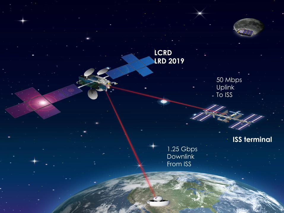
1.25 Gbps Downlink From ISS
50 Mbps Uplink To ISS
LCRD LRD 2019
ISS terminal
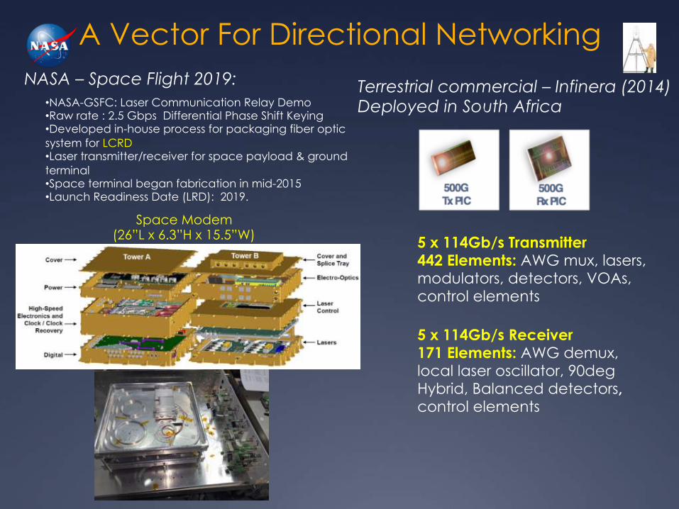
A Vector For Directional Networking
• NASA-GSFC: Laser Communication Relay Demo • Raw rate : 2.5 Gbps Differential Phase Shift Keying • Developed in-house process for packaging fiber optic system for LCRD • Laser transmitter/receiver for space payload & ground terminal • Space terminal began fabrication in mid-2015 • Launch Readiness Date (LRD): 2019.
Space Modem (26”L x 6.3”H x 15.5”W)
Terrestrial commercial – Infinera (2014) Deployed in South Africa
NASA – Space Flight 2019:
5 x 114Gb/s Transmitter 442 Elements: AWG mux, lasers, modulators, detectors, VOAs, control elements
5 x 114Gb/s Receiver 171 Elements: AWG demux, local laser oscillator, 90deg Hybrid, Balanced detectors, control elements
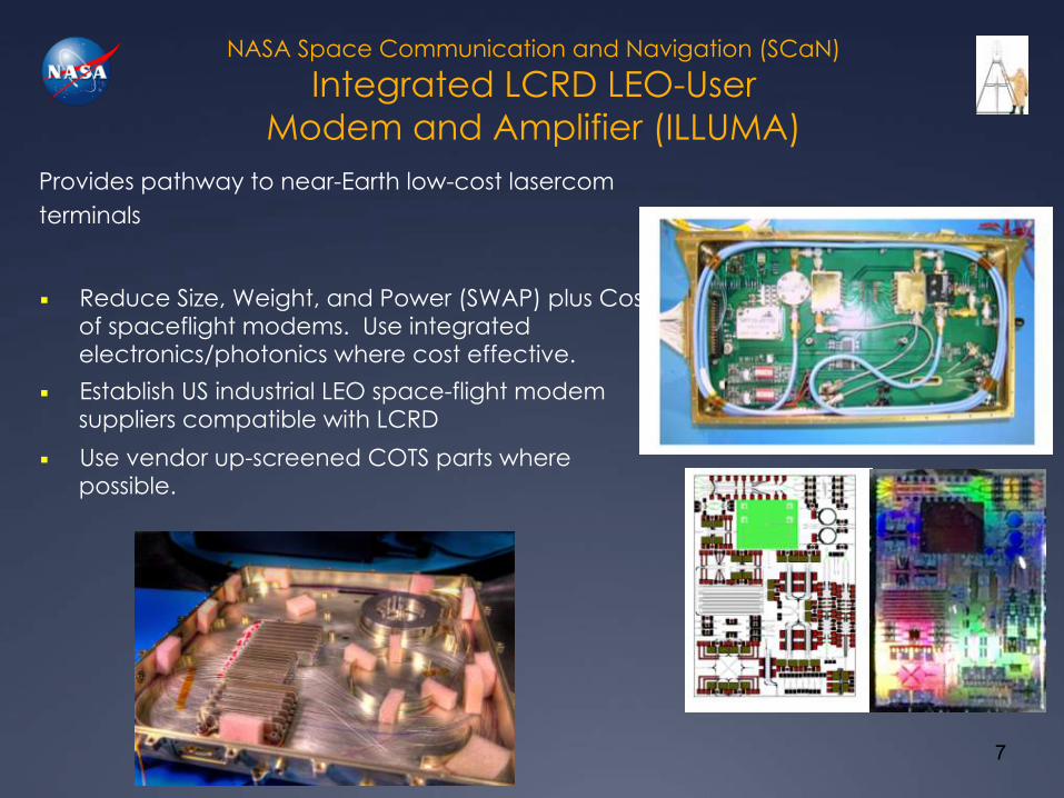
NASA Space Communication and Navigation (SCaN)
Integrated LCRD LEO-User Modem and Amplifier (ILLUMA)
Provides pathway to near-Earth low-cost lasercom terminals
▪ Reduce Size, Weight, and Power (SWAP) plus Cost
of spaceflight modems. Use integrated electronics/photonics where cost effective.
▪ Establish US industrial LEO space-flight modem suppliers compatible with LCRD
▪ Use vendor up-screened COTS parts where possible.
7

Transmitter front-end PIC DFB with Integrated MZ modulator
(need high extinction ratio ~20 dB) Comparison of integrated InP to LiNbO3 DE VALICOURT et al.: MONOLITHIC INTEGRATED INP TRANSMITTERS USING SWITCHING OF PREFIXED OPTICAL PHASES 665
Fig. 2. (a) A cross-view of a SI buried ridge. (b) Transmitter chip mounted on HF submount. Photographies of integrated (c) BPSK & 2ASK-2PSK transmitter,(d) QPSK transmitter and (e) packaged QPSK transmitter.
passive and different active regions made of AlGaInAs multi-quantum wells. In SAG, different areas of material optimized foractive or passive optical function are defined in a single epitaxialstep by use of dielectric masks that locally enhance growth rate.Unlike the Butt-joint technique, self-aligned and genuinely con-tinuous SAG guide avoids reflection between each area whateverwas the number of engineered bandgaps. The simulated photo-luminescence wavelength for each photonic function area of thefour-arm integrated transmitter has been calculated and moredetails could be found in [8]. Up to five different material gapsare designed and realized for this circuit with SAG (laser, EAM,VOA, SOA and transparent waveguides). The two-arm circuit issimpler and required three different material gaps (laser, EAMand transparent waveguides).
Second epitaxial technique used in the realization process ofthe component is the Semi Insulating Buried heterostructure forlow RC product EAMs. In addition to its simplicity (only onesingle regrowth for all PIC components), it enhances the chip ro-bustness, thermal dissipation and current confinement. A cross-view of a semi insulating-buried ridge is shown on Fig. 2 (a).A blocking layer prevents the inter-diffusion between the semiinsulating InP and the upper p-doped InP which finishes to buryall the structure. The final device was coated with a high reflec-tion coating on the laser side and with an anti-reflection coatingon the output guide. Finally, the device is mounted on a highfrequency submount in order to perform high speed measure-ments, Fig. 2(b). The QPSK transmitter has been assembled ina standard LiNbO3 package providing dc and high frequencyconnections. In Fig. 2(e), the chip is displayed in its large box,suggesting ∼100 times footprint reduction with InP technologyas compared to conventional unintegrated photonic components.
The monolithic two-arm interferometer transmitter is repre-sented in Fig. 2(c). It includes eight components on chip suchas three passives (two MMI, one taper) and five actives (onelaser, two EAM and two PSs). The propagation loss split is as
follows: 2.5 dB for linear waveguide, 2 × 0.5 dB for waveguidebends, 2 × 0.5 dB for MMI excess loss and 0.5 dB for on-stateEAMs. The output power coupled into the fiber for constructiveinterference state and unbiased EAMs at 150 mA laser-biasedcurrent was measured to be +2 dBm, under modulation theaverage coupled optical power is –5 dBm. The circuit dimen-sions are 2.65 mm × 0.5 mm, making it the smallest reported100 Gb/s PSK-capable integrated transmitter, to the best of ourknowledge.
For the QPSK transmitter, the four waveguides are then com-bined by a two-stage 2:1 MMI into a single output. The totalchip size is 5200 µm length and 500 µm width, which makes it,again to the best of our knowledge, the smallest reported QPSKtransmitter [see Fig. 2(d)]. The loss split is as follows: 6.5 dB forlinear waveguide, 3×0.5 dB for waveguide bends, 3 × 0.5 dBfor MMI excess loss and 0.5 dB for on-state EAMs. A SOA wasintegrated to compensate for partially such losses. Therefore thecontinuous wave optical power coupled into the fiber was also+2 dBm however the optical output power under modulationwas reduced to −9 dBm. Low bias current was used for theSOA to prevent laser oscillations due to the non-ideal fabrica-tion process. The chip integrates in total 19 components: fivepassive (four MMI and one taper) and 14 active (one laser, fourEAM, four variable optical attenuators, four PSs and one SOA).For the two-arms transmitters, the quality of the output signalmainly depends on the SMSR of the laser. For the four-armstransmitter, the output optical signal-to-noise ratio (OSNR) isreduced due to the extra noise added by the SOA resulting ofaround 20 dB OSNR.
III. INTEGRATED TRANSMITTER CHARACTERISTIC
Moving to a real device induces different sources of distor-tions which may be considered when looking for the most effi-cient configuration. Device limitations can be mainly attributed
JOURNAL OF LIGHTWAVE TECHNOLOGY, VOL. 33, NO. 3, FEBRUARY 1, 2015 663
Monolithic Integrated InP Transmitters UsingSwitching of Prefixed Optical Phases
Guilhem de Valicourt, Haik Mardoyan, M. A. Mestre, P. Jenneve, J. C. Antona, S. Bigo, O. Bertran-Pardo,Christophe Kazmierski, J. Decobert, N. Chimot, and F. Blache
Abstract—Recent progresses on monolithic InP integration arepresented for achieving high-performance transmitters for cost-sensitive metropolitan networks. We demonstrate the generationof advanced modulation format using two types of integrated trans-mitters with prefixed optical phases. Complex modulation formatsare generated with constellations exploiting the whole complexplane such as BPSK, quadrature phase-shift keying, N-QIM, and2ASK-2PSK modulation. We achieve data rate up to 224 Gb/s using2ASK-2PSK modulation with polarization division multiplexing.Finally, we assess its suitability for metropolitan networks with alarge number of cascaded nodes.
Index Terms—Coherent communications, integrated opticsdevices.
I. INTRODUCTION
COHERENT technologies have been revolutionizing op-tical core networks and are expected to conquer a large
market share in metropolitan and inter-datacenter networks inthe very near future. However, these segments are particularlysensitive to cost, and therefore to footprint and power consump-tion, while possibly facing stringent requirements from largercascades of optical nodes than in core networks.
In order to contain cost, several chips can be co-packagedin the optoelectronic transmitter. For example, in [1], laser andmodulator chips were co-packaged and produced optical dataat 32 GBaud. However, monolithic integration is expected toprovide larger cost savings than co-packaging. The first gen-eration of monolithically integrated transmitters was inspiredby LiNbO3 modulators, based on Mach–Zehnder modulators(MZMs) and designed with Indium Phosphide (InP) technol-ogy. In [2], four of such MZMs were integrated with the cor-responding lasers and an optical multiplexer, but the outputsymbol rate did not exceed 14.3 Gbaud per laser. More re-cently, a monolithic transmitter incorporating a MZM witha sampled grating-distributed Bragg reflector tunable laser, a
Manuscript received June 1, 2014; revised September 5, 2014; accepted Oc-tober 7, 2014. Date of publication October 14, 2014; date of current versionFebruary 17, 2015. This work was supported by IST-257980 MIRTHE project.
G. de Valicourt was with the Alcatel-Lucent Bell Labs France, 91620 Nozay,France. He is now with Bell Labs, Alcatel-Lucent, NJ 07733 Holmdel, USA(e-mail: [email protected])
H. Mardoyan, M. A. Mestre, P. Jenneve, J. C. Antona, and S. Bigo arewith the Alcatel-Lucent Bell Labs France, 91620 Nozay, France (e-mail:[email protected]).
O. Bertran-Pardo is with Alcatel-Lucent, Route de Villejust, Nozay, France.C. Kazmierski, J. Decobert, N. Chimot, and F. Blache are with III-V lab, a
joint Laboratory of Alcatel-Lucent Bell Labs, Thales Research & Technologyand CEA-Leti, Campus Polytechnique, 1, Avenue A. Fresnel, 91767 Palaiseaucedex, France (e-mail: [email protected]).
Color versions of one or more of the figures in this paper are available onlineat http://ieeexplore.ieee.org.
Digital Object Identifier 10.1109/JLT.2014.2363104
semiconductor optical amplifier, and an absorber was reportedand produced data streams at 10 Gbaud [3]. Here again, de-spite the high level of integration, the transmitter was lim-ited in terms of modulation bandwidth by the MZM. A recordbandwidth operation of transmitter photonic integrated circuits(PICs) (28 Gbaud/wavelength) was demonstrated however itsperformances in optical transmission systems still need to beassessed [4]. To extend this bandwidth while further reduc-ing footprint, short electro-absorption modulators (EAM) arenatural candidates, but act primarily as intensity modulators.However, several EAMs in an interferometric arrangement canproduce complex amplitude/phase modulation [5], [6]. We builtupon this principle our two previous reports where we showedthat a monolithic chip incorporating two EAMs and a lasersource could be used to deliver 12.5 Gbaud binary phase shiftkeying (BPSK) [7] and 28 Gbaud polarization division mul-tiplexed (PDM) -BPSK [8]. Both proof-of-concept papers fellshort of the requirements of metropolitan optical terrestrial (only40 km distance shown at 12.5 Gb/s).
In order to modulate light along the positive and negativeparts of one single axis, the combination of two intensity mod-ulators with a phase difference of 180° is needed. With thisapproach, we demonstrated modulation formats such as BPSKor two-level amplitude shift keying (2ASK), two-level phaseshift keying (2PSK) 2ASK-2PSK by driving the modulatorswith DACs [9]. We can also generate non-quadrature intensitymodulation (N-QIM) formats in the complex plane (2-D) withthe limited number of two intensity modulators and a phaseshift different than 180° between both arms; however the imple-mentation of such scheme based on photonic integration inducesextra-penalties due to non-ideal devices. Therefore 2ASK-2PSKremains the less noise sensitive four-symbol modulation for-mat which however requires 4-level electrical signals. In orderto achieve quadrature phase-shift keying (QPSK) modulationwith intensity modulators, the obvious solution consists of us-ing four modulators with phase shifts of 0 and 180° on the onehand, and 90° and 270° on the other hand. Such InP-monolithicQPSK transmitter is achieved at the expense of a more complex4-arms interferometer device which integrates 19 components.130 Gb/s data-rate on a single wavelength is demonstrated usingsuch transmitter; however a relatively large linewidth and lowpower of the laser were limiting the propagation distance [10].
In order to cope with the metropolitan network requirements,we propose to use the 2ASK-2PSK modulation format andachieve a record 224 Gb/s bit-rate per wavelength for mono-lithic transmitter. We then show the robustness of the generatedsignal to narrow filtering in optical nodes.
0733-8724 © 2014 IEEE. Personal use is permitted, but republication/redistribution requires IEEE permission.See http://www.ieee.org/publications standards/publications/rights/index.html for more information.

Coherent receiver PIC
6100108 IEEE JOURNAL OF SELECTED TOPICS IN QUANTUM ELECTRONICS, VOL. 20, NO. 4, JULY/AUGUST 2014
Fig. 3. Polarization-diversity coherent receiver using Si PIC. (a) Photonic cir-cuit diagram. PBS: polarization beam splitter; PR: polarization rotator; TIA:transimpedance amplifier. (b) Photograph of the receiver PIC. PD: photo detec-tor; IT: inverse taper; MMI: multimode interference coupler. (c) Photograph ofthe packaged coherent receiver. PCB: printed circuit board.
The receiver PIC consists of two inverse tapers, two polar-ization beam splitters (PBSs), two polarization rotators, twomultimode-interference coupler (MMI) 90◦ hybrids and eightgermanium PDs. Fig. 3(a) and (b) shows the circuit diagramand the photograph of the fabricated PIC, respectively. Boththe transmitter and receiver PICs share the same design of po-larization rotators; the PBC and PBS are identical. The overallchip size is 1.3 mm × 3 mm. The silicon PIC was packagedwith two SiGe dual-channel transimpedance amplifiers (TIAs)whose circuit architectures were presented in [41]. The PIC waswire-bonded to two dual-TIA chips, as shown in Fig. 3(c).
The principle of operation is as follows. The optical signalwith two polarizations is coupled into the signal port of thereceiver PIC while the optical local oscillator (LO) is coupledinto the Si PIC through the other port. Once coupled in, the signaland LO are divided into TE and TM polarizations through twoPBSs. The TE polarized lights proceed to the 4 × 4 MMI-based90-degree hybrids, whose four outputs are detected by four GePDs on the left side of the PIC [see Fig. 3(b)]. The detectionby two balanced PD pairs produces the in-phase and quadraturecomponents of the TE-polarization. The TM components fromthe output of PBSs are converted to TE polarization by twopolarization rotators. The converted TE lights enter the right-side 4 × 4 MMI-based 90◦ hybrid, which is identical to thatfor the TE mode. The in-phase and quadrature components ofthe TM-polarization are then detected by the same detectionscheme as that used for the TE mode.
III. 224-GB/S PDM-16-QAM GENERATION
To generate coherent signals, a CW laser at 1539.77 nm waslaunched into the transmitter PIC in the TE mode. The four mod-ulators were driven by four RF signals, each generated by four7-bit digital-analog-converters (DACs) and amplified by fourRF amplifiers to a peak-to-peak voltage swing of ∼5 V. To en-
Fig. 4. 28-Gbaud PDM-QPSK and PDM-16-QAM generation using sili-con PIC. (a) BER versus OSNR, (b) and (c) QPSK constellations, (d) and(e) 16-QAM constellations. Inset: the optical spectrum of the PDM-16-QAMsignal.
able high spectral efficiency wavelength-division multiplexing,digital signal processing (DSP) was performed to form Nyquistpre-filtered driving signals with a roll-off factor of 0.1 [46].The DACs were operating at 56 GSamples/s to provide a mod-ulation speed of 28 Gbaud when an oversampling ratio of twowas used. The original data sequences used for constellationmapping were pseudo-random bit sequences (PRBS) of length215–1. Digital coherent detection was carried out by using a50-GSamples/s digital sampling oscilloscope, followed by of-fline DSP using common signal recovery algorithms such aschannel equalization and polarization de-multiplexing based onconstant-modulus algorithm and multi-modulus algorithm, fre-quency estimation and compensation, and carrier phase estima-tion and compensation [37].
The performance of the transmitter PIC was first character-ized using a commercial coherent optical receiver frontend.Fig. 4 shows the performance of the generated PDM-QPSKand PDM-16-QAM signals. The recovered signal constellationsin Fig. 4(b-e) show the successful signal generation, while thespectrum (inset) exhibits the Nyquist spectral shaping (NSS).The bit error ratio (BER), calculated by direct error counting,
6100108 IEEE JOURNAL OF SELECTED TOPICS IN QUANTUM ELECTRONICS, VOL. 20, NO. 4, JULY/AUGUST 2014
Monolithic Silicon Photonic Integrated Circuitsfor Compact 100+Gb/s Coherent Optical
Receivers and TransmittersPo Dong, Member, IEEE, Xiang Liu, Senior Member, IEEE, S. Chandrasekhar, Fellow, IEEE, Lawrence L. Buhl,
Ricardo Aroca, and Young-Kai Chen, Fellow, IEEE
(Invited Paper)
Abstract—We present silicon photonic integrated circuits (PICs)based coherent optical transmitters and receivers for high-speedlong-distance fiber optical transmission. High-degree photonic in-tegration is achieved by monolithically integrating silicon electro-optic modulators, germanium photo detectors, silicon nitride-assisted on-chip polarization rotators, thermal phase shifters, andvarious passive silicon optical devices on a single wafer platform.We demonstrate the use of these PICs for modulating and detect-ing 112-Gb/s polarization-division-multiplexed quadrature phase-shift keying (PDM-QPSK) and 224-Gb/s PDM 16-ary quadratureamplitude modulation (PDM-16-QAM) signals. Transmission andcoherent detection of a 112-Gb/s PDM-QPSK signal over 2560-kmstandard single-mode fiber is also demonstrated. The high-degreephotonic integration for silicon PICs promises small-form-factorand low-power-consumption transceivers for future coherent sys-tems that demand high cost efficiency and energy efficiency.
Index Terms—Photonic integrated circuits, silicon photonics, co-herent communications, waveguide modulators, optoelectronics,coherent receivers.
I. INTRODUCTION
G LOBAL information communications demand opticaltransmission systems with high spectral efficiency, high
channel data rate, and low cost [1]–[3]. Recent advances inoptical modulation formats, together with wavelength-divisionand polarization-division multiplexing, are key enablers to in-crease the spectral efficiency and the data rates. Coherent opti-cal transmission has become a key technology for high-capacitylong-haul communications with channel data rates at 100 Gb/sand beyond [3]–[5]. Polarization-division-multiplexed quadra-ture phase-shift keying (PDM-QPSK) has been utilized in thecurrent 100-Gb/s networks. Next-generation transport networks
Manuscript received October 21, 2013; revised December 10, 2013; acceptedDecember 11, 2013. Date of current version January 9, 2014.
P. Dong, X. Liu, S. Chandrasekhar, and L. L. Buhl are with Bell Labs,Alcatel-Lucent, Holmdel, NJ 07733 USA (e-mail: [email protected]; [email protected]; [email protected]; [email protected]).
R. Aroca and Y.-K. Chen are with Bell Labs, Alcatel-Lucent, MurrayHill, NJ 07974 USA (e-mail: [email protected]; [email protected]).
Color versions of one or more of the figures in this paper are available onlineat http://ieeexplore.ieee.org.
Digital Object Identifier 10.1109/JSTQE.2013.2295181
may utilize even higher-level modulation formats, such as 16-aryquadrature amplitude modulation (16-QAM). With its embed-ded high capacity, cost-effective electronic equalization of fiberimpairments, and network monitoring capabilities, the coher-ent transmission technology is also well-suited for metro andshorter-reach networks [6].
The key components that enable coherent optical transmissionare coherent optical receivers and transmitters, typically consist-ing of a number of high-performance optical components, suchas narrow linewidth lasers, high-speed modulators, high-speedphoto detectors (PDs), polarization beam splitters/combiners(PBS/C), polarization rotators, and 90◦optical hybrids. The first-generation coherent transceivers in long-haul systems are imple-mented by selective discrete optical components with optimizedperformance for meeting the very challenging transmission re-quirements. Low-cost, energy-efficient, and compact coherenttransceivers are needed for the future coherent transmissionsystems.
Several hybrid optical integration technologies have beenexplored to demonstrate coherent transmitters and receivers.For example, silica or polymer planar lightwave circuits havebeen co-packaged with LiNbO3 (LN) [7], [8] or indium phos-phide (InP) modulators [9], or have been assembled with photo-detectors [10]–[16]. Although the overall optical device sizesmay be small enough for next-generation transceivers, the pack-aging cost could be a concern.
Higher-degree photonic integration can be achieved by III-V(mainly InP or GaAs) and silicon photonic integrated circuits(PICs). The PICs could significantly reduce the device sizesand simplify the packaging procedures. InP-based PICs havebeen realized to integrate high-speed modulators or PDs, wave-length multiplexing filters, and integrated lasers on the same chip[17]–[31]. However, to the best of our knowledge, on-chip po-larization rotators and PBS/Cs have not yet been integrated intocoherent transmitters and receivers, even though integrated po-larization elements have been reported in InP-based DQPSKreceivers in [32].
Silicon PIC shows very promising progress for coherenttransceivers. Recently, QPSK modulated optical signals weregenerated by compact silicon microring modulators [33], [34]as well as silicon Mach-Zehnder modulators (MZMs) [35]. Byfurther integrating two in-phase/quadrature (I/Q) modulatorswith an on-chip polarization rotator and a PBC, a monolithic
1077-260X © 2014 IEEE. Personal use is permitted, but republication/redistribution requires IEEE permission.See http://www.ieee.org/publications standards/publications/rights/index.html for more information.

Receiver preamplifier PIC
Erbium-doped spiral amplifiers with 20 dB of net gain on silicon
Sergio A. Vázquez-Córdova,1,2,* Meindert Dijkstra,1,2 Edward H. Bernhardi,1 Feridun Ay,1,3 Kerstin Wörhoff,1 Jennifer L. Herek,2 Sonia M. García-Blanco,1,2 and
Markus Pollnau1,4 1Integrated Optical MicroSystems Group, MESA + Institute for Nanotechnology, University of Twente, P.O. Box 217,
7500 AE Enschede, The Netherlands 2Optical Sciences Group, MESA + Institute for Nanotechnology, University of Twente, P.O. Box 217, 7500 AE
Enschede, The Netherlands 3Department of Electrical and Electronics Engineering, Anadolu University, 26555 Eskişehir, Turkey
4Department of Materials and Nano Physics, School of Information and Communication Technology, KTH−Royal Institute of Technology, Electrum 229, Isafjordsgatan 22−24, 16440 Kista, Sweden
Abstract: Spiral-waveguide amplifiers in erbium-doped aluminum oxide on a silicon wafer are fabricated and characterized. Spirals of several lengths and four different erbium concentrations are studied experimentally and theoretically. A maximum internal net gain of 20 dB in the small-signal-gain regime is measured at the peak emission wavelength of 1532 nm for two sample configurations with waveguide lengths of 12.9 cm and 24.4 cm and concentrations of 1.92 × 1020 cm−3 and 0.95 × 1020 cm−3, respectively. The noise figures of these samples are reported. Gain saturation as a result of increasing signal power and the temperature dependence of gain are studied. ©2014 Optical Society of America OCIS codes: (130.0130) Integrated optics; (140.4480) Optical amplifiers; (160.5690) Rare-earth-doped materials; (130.2755) Glass waveguides.
References and links 1. R. Soulard, A. Zinoviev, J. L. Doualan, E. Ivakin, O. Antipov, and R. Moncorgé, “Detailed characterization of
pump-induced refractive index changes observed in Nd:YVO4, Nd:GdVO4 and Nd:KGW,” Opt. Express 18(2), 1553–1568 (2010).
2. J. D. B. Bradley, M. Costa e Silva, M. Gay, L. Bramerie, A. Driessen, K. Wörhoff, J. C. Simon, and M. Pollnau, “170 Gbit/s transmission in an erbium-doped waveguide amplifier on silicon,” Opt. Express 17(24), 22201–22208 (2009).
3. S. Blaize, L. Bastard, C. Cassagnetes, and J. E. Broquin, “Multiwavelengths DFB waveguide laser arrays in Yb-Er codoped phosphate glass substrate,” IEEE Photon. Technol. Lett. 15(4), 516–518 (2003).
4. E. H. Bernhardi, H. A. van Wolferen, L. Agazzi, M. R. Khan, C. G. Roeloffzen, K. Wörhoff, M. Pollnau, and R. M. de Ridder, “Ultra-narrow-linewidth, single-frequency distributed feedback waveguide laser in Al2O3:Er3+ on silicon,” Opt. Lett. 35(14), 2394–2396 (2010).
5. D. Geskus, S. Aravazhi, S. M. García-Blanco, and M. Pollnau, “Giant optical gain in a rare-earth-ion-doped microstructure,” Adv. Mater. 24(10), OP19–OP22 (2012).
6. Y. C. Yan, A. J. Faber, H. de Waal, P. G. Kik, and A. Polman, “Erbium-doped phosphate glass waveguide on silicon with 4.1 dB/cm gain at 1.535 µm,” Appl. Phys. Lett. 71(20), 2922–2924 (1997).
7. L. H. Slooff, M. J. A. de Dood, A. van Blaaderen, and A. Polman, “Effects of heat treatment and concentration on the luminescence properties of erbium-doped silica sol-gel films,” J. Non-Cryst. Solids 296(3), 158–164 (2001).
8. J. Yang, M. B. J. Diemeer, D. Geskus, G. Sengo, M. Pollnau, and A. Driessen, “Neodymium-complex-doped photodefined polymer channel waveguide amplifiers,” Opt. Lett. 34(4), 473–475 (2009).
9. K. Wörhoff, J. D. B. Bradley, F. Ay, D. Geskus, T. P. Blauwendraat, and M. Pollnau, “Reliable low-cost fabrication of low-loss Al2O3:Er3+ waveguides with 5.4-dB optical gain,” IEEE J. Quantum Electron. 45(5), 454–461 (2009).
10. L. Agazzi, J. D. B. Bradley, M. Dijkstra, F. Ay, G. Roelkens, R. Baets, K. Wörhoff, and M. Pollnau, “Monolithic integration of erbium-doped amplifiers with silicon-on-insulator waveguides,” Opt. Express 18(26), 27703–27711 (2010).
#221324 - $15.00 USD Received 19 Aug 2014; revised 24 Sep 2014; accepted 3 Oct 2014; published 15 Oct 2014(C) 2014 OSA 20 October 2014 | Vol. 22, No. 21 | DOI:10.1364/OE.22.025993 | OPTICS EXPRESS 25993
Fig. 1. (a) Waveguide amplifier cross-section and simulated signal-mode profile. (b)
Photograph of a pumped (λP = 976 nm) Al2O3:Er3+
spiral amplifier on a silicon chip. A close-
up view of the spiral amplifier is shown in the inset.
Understanding the performance of an Er3+
-doped amplifier is significantly complicated by
the spectroscopic processes of the Er3+
ion. The migration-accelerated ETU process (4I13/2,
4I13/2) → (
4I15/2,
4I9/2) induces a concentration- and excitation-dependent quenching of the
4I13/2
amplifier level. More importantly, a fast quenching process of this level occurs in SiO2 [11],
Al2O3:Er3+
[13], and potentially other Er3+
-doped materials, which limits the optimum Er3+
concentration in Al2O3 to 1−2 × 10²⁰
cm−3
. As a consequence, waveguide lengths on the order
of 10 cm are desired for efficient amplifier performance.
Al2O3 layers with Er3+
concentrations of 0.45 × 10²⁰
cm−3
, 0.95 × 10²⁰
cm−3
, 1.92 × 10²⁰
cm−3
, and 3.0 × 10²⁰
cm−3
were deposited onto thermally oxidized silicon substrates by RF
reactive co-sputtering [9]. For each of the four different doping concentrations, spiral-shaped
channel waveguides with different lengths varying from 12.9 cm to 41.6 cm were patterned
into the Al2O3:Er3+
layers using standard lithographic techniques and chlorine-based reactive
ion etching [24]. The spiral shape [Fig. 1(b)] minimizes the device foot print. A minimum
bending radius of R = 2 mm was selected. For this radius, the simulated additional bending
loss of <10−6
dB/cm is negligible compared to the straight-waveguide propagation loss of
~0.1 dB/cm and the mode-mismatch loss of ~0.02 dB at the junction in the center of the
spiral. Transverse-electric (TE) polarization was chosen for signal and pump light in the
simulations and measurements.
A 5-μm-thick SiO2 layer was deposited on top of each patterned Al2O3 layer by PECVD
as a protective cladding. Finally, waveguide end faces were prepared by dicing.
3. Propagation losses
The non-destructive method proposed by Okamura et al. [28] was applied to investigate the
propagation loss in our devices. The method consists of capturing a top-view image (InGaAs
camera Sensors Inc. SU320M-1.7RT, 320 × 240 px.) of the infrared light (λ = 1320 nm,
Amoco laser model D200) scattered from a quarter of the spiral waveguide, as shown in Fig.
2(a). The wavelength selected for this experiment lies outside the Er3+
absorption bands and,
thus, the passive characteristics can be determined. Background propagation losses around
1530 nm are expected to be similar to those at 1320 nm and 0.18 dB/cm higher at 980 nm due
to Rayleigh scattering [23]. A spatial calibration of the image was readily performed, since
the dimensions of the spirals are well known from the lithographic mask. It was assumed that
in average the intensity of scattered light is proportional to the intensity of light propagating
within the channel. This is the case if the scattering centers (such as channel interface
#221324 - $15.00 USD Received 19 Aug 2014; revised 24 Sep 2014; accepted 3 Oct 2014; published 15 Oct 2014(C) 2014 OSA 20 October 2014 | Vol. 22, No. 21 | DOI:10.1364/OE.22.025993 | OPTICS EXPRESS 25996
• Internal net gain = 20 dB • Noise figure of 3.75 dB small-signal-gain regime.

Fused Silica Witness Sample Etched by Femtosecond Laser
Dielectric Breakdown of Air at Laser Focus
Goddard Code 554 Femtosecond Direct-Write laser

Direct-write laser system is multi-use
Optical waveguides Precision Machining Patterning graphene
Milling/Bonding/welding glass Glass/copper weld Additive manufacturing with laser sintering (3D printer principle)

Direct write waveguide fabrication
Making lasers with a laser

NASA Space Technology Mission Directorate (STMD) Early Stage Innovation (ESI)
Integrated Photonics for Space Communication
Ü Karen Bergman, Columbia University
Ultra-Low Power CMOS-Compatible Integrated-Photonic Platform for Terabit-Scale Communications
Ü Seng-Tiong Ho, Northwestern University
Compact Robust Integrated PPM Laser Transceiver Chip Set with High Sensitivity, Efficiency, and Reconfigurability
Ü Jonathan Klamkin, University of California-Santa Barbara,
PICULS: Photonic Integrated Circuits for Ultra-Low size, Weight, and Power
Ü Paul Leisher, Rose-Hulman Institute of Technology
Integrated Tapered Active Modulators for High-Efficiency Gbps PPM Laser Transmitter PICs
Ü Shayan Mookherjea, University of California-San Diego
Integrated Photonics for Adaptive Discrete Multi-Carrier Space-Based Optical Communication
and Ranging

Acknowledgments
NASA STMD
NASA SCaN
DoD IP-IMI
AETD colloquium
Thank you!