presentación de powerpoint - aalto · plasma enhanced chemical vapor deposition (pecvd) ......
TRANSCRIPT
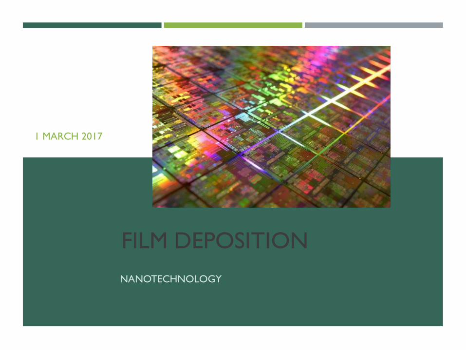
FILM DEPOSITION
1 MARCH 2017
NANOTECHNOLOGY
PRESENTATION
Pedro C. Feijoo
E-mail: [email protected]
FABRICATION TECHNOLOGIES FOR NANOELECTRONIC DEVICES. PEDRO C. FEIJOO 2
FILM GROWTH
Chemical vapor deposition (CVD)/Vapor phase epitaxy (VPE)
Atmospheric pressure CVD (APCVD)
Low pressure CVD (LPCVD)
Metal organic chemical vapor deposition (MOCVD)
Plasma enhanced chemical vapor deposition (PECVD)
Atomic layer deposition (ALD)
Physical vapor deposition (PVD)
Evaporation
Sputtering
Pulsed laser deposition/Laser sputtering/Laser ablation deposition (PLD)
Molecular beam epitaxy (MBE)
Electrochemical forming
Electrodeposition
FABRICATION TECHNOLOGIES FOR NANOELECTRONIC DEVICES. PEDRO C. FEIJOO 3
OUTLINE
1. CONCEPTS
2. TYPES OF TECHNIQUES
3. TECHNIQUES
FABRICATION TECHNOLOGIES FOR NANOELECTRONIC DEVICES. PEDRO C. FEIJOO 4
CONCEPTS
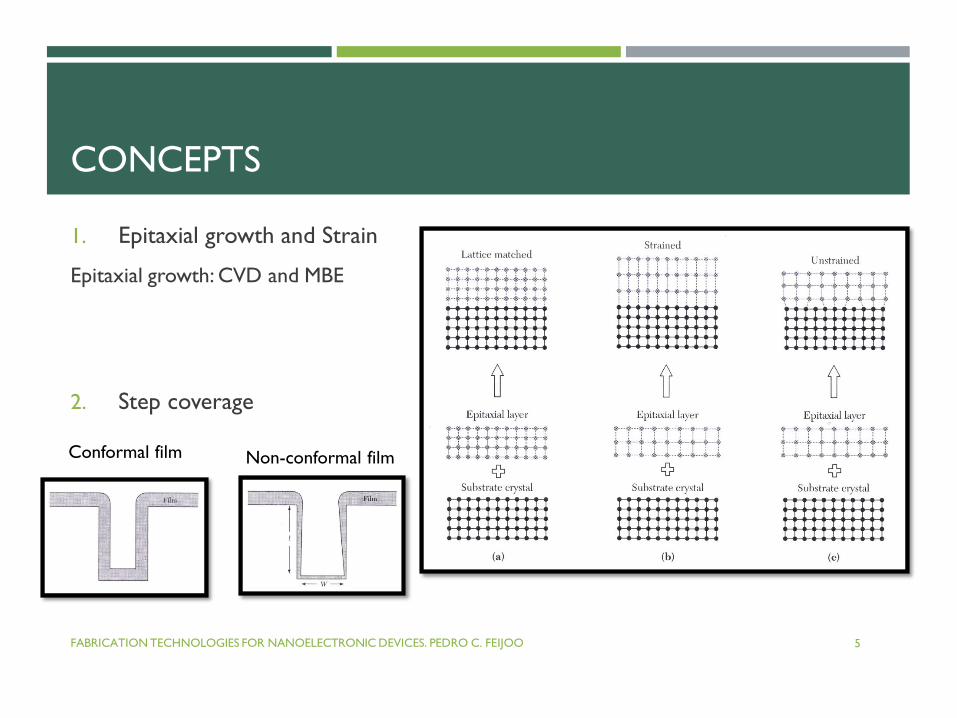
1. Epitaxial growth and Strain
Epitaxial growth: CVD and MBE
2. Step coverage
FABRICATION TECHNOLOGIES FOR NANOELECTRONIC DEVICES. PEDRO C. FEIJOO 5
Conformal film Non-conformal film
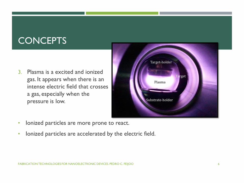
3. Plasma is a excited and ionized
gas. It appears when there is an
intense electric field that crosses
a gas, especially when the
pressure is low.
• Ionized particles are more prone to react.
• Ionized particles are accelerated by the electric field.
CONCEPTS
FABRICATION TECHNOLOGIES FOR NANOELECTRONIC DEVICES. PEDRO C. FEIJOO 6
FILM GROWTH CLASSIFICATION
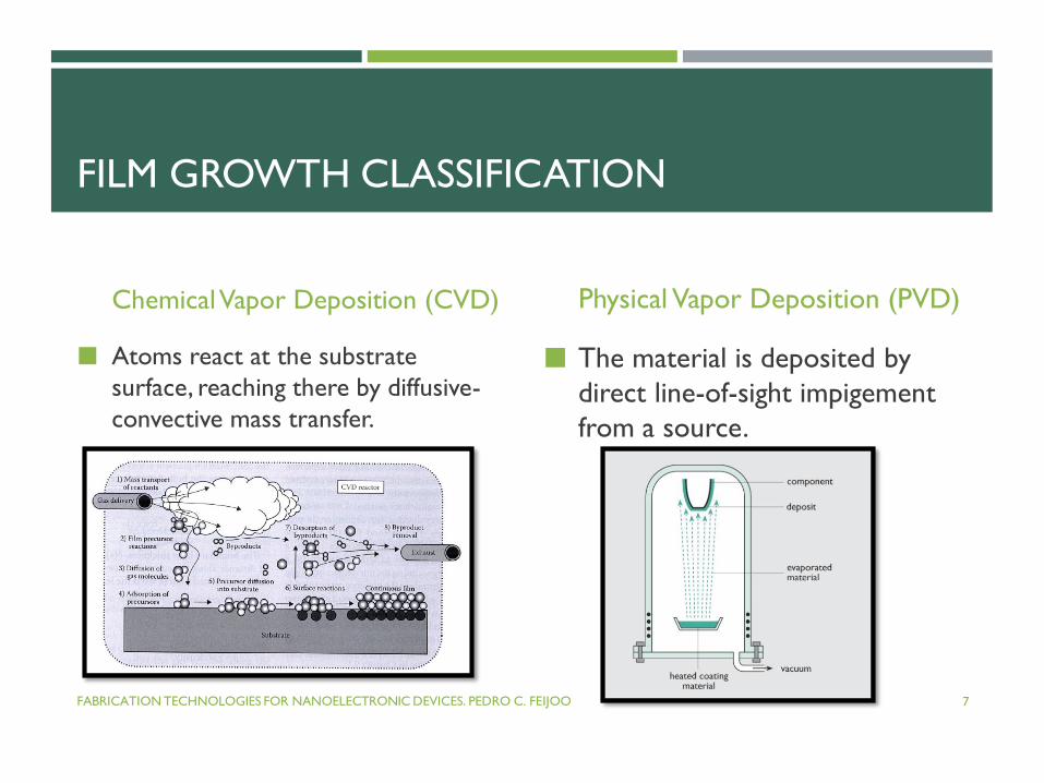
ChemicalVapor Deposition (CVD)
Atoms react at the substrate
surface, reaching there by diffusive-
convective mass transfer.
Physical Vapor Deposition (PVD)
The material is deposited by
direct line-of-sight impigement
from a source.
FABRICATION TECHNOLOGIES FOR NANOELECTRONIC DEVICES. PEDRO C. FEIJOO 7
FILM GROWTH CLASSIFICATION
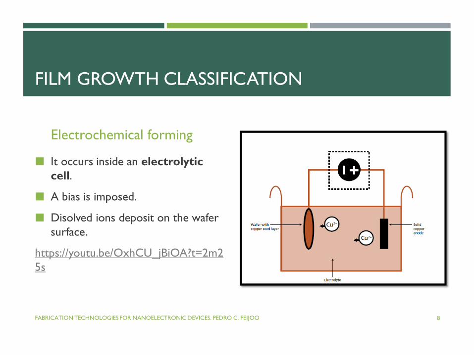
Electrochemical forming
It occurs inside an electrolytic
cell.
A bias is imposed.
Disolved ions deposit on the wafer
surface.
https://youtu.be/OxhCU_jBiOA?t=2m2
5s
FABRICATION TECHNOLOGIES FOR NANOELECTRONIC DEVICES. PEDRO C. FEIJOO 8
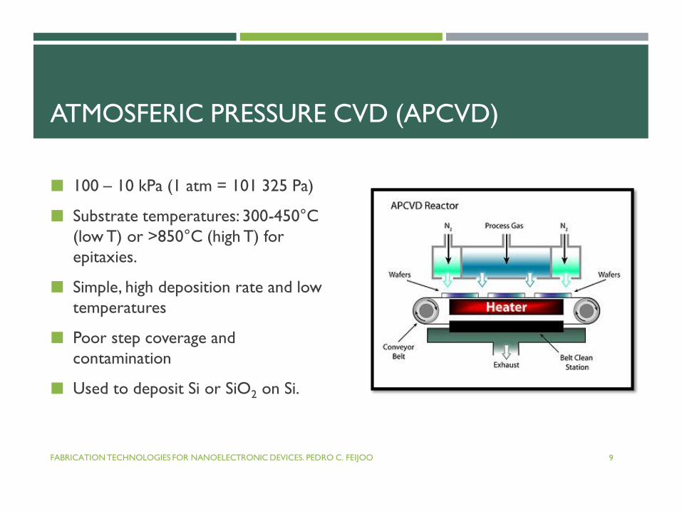
ATMOSFERIC PRESSURE CVD (APCVD)
100 – 10 kPa (1 atm = 101 325 Pa)
Substrate temperatures: 300-450°C
(low T) or >850°C (high T) for
epitaxies.
Simple, high deposition rate and low
temperatures
Poor step coverage and
contamination
Used to deposit Si or SiO2 on Si.
FABRICATION TECHNOLOGIES FOR NANOELECTRONIC DEVICES. PEDRO C. FEIJOO 9
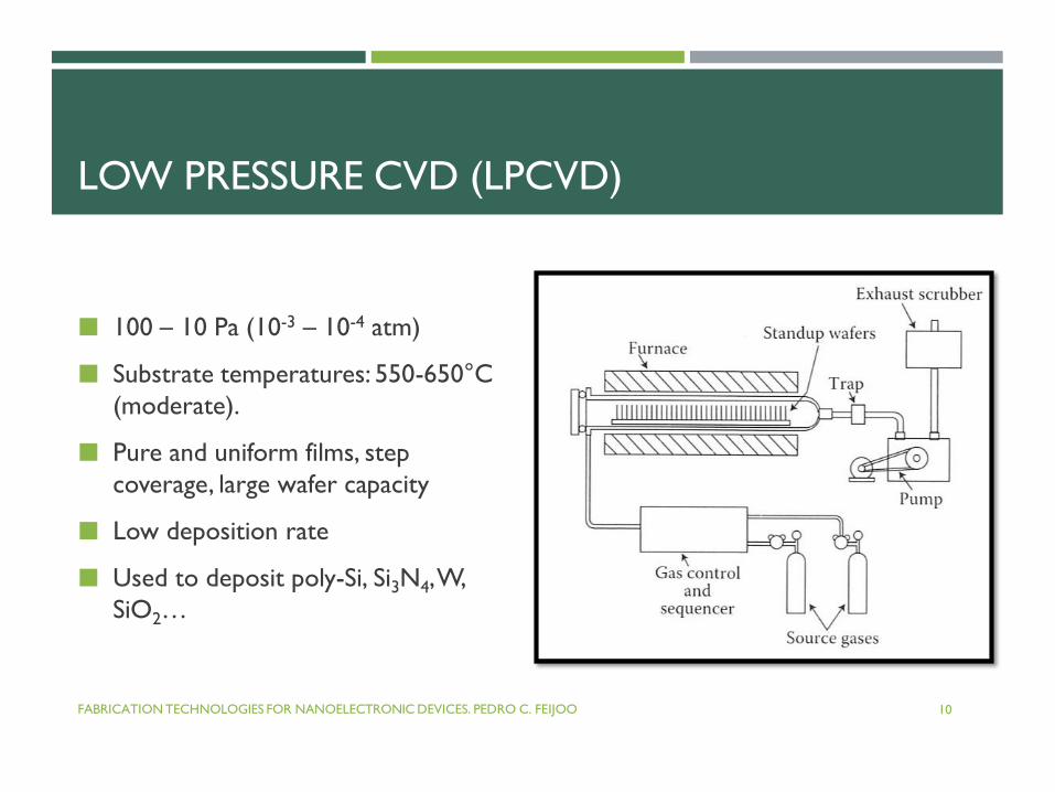
LOW PRESSURE CVD (LPCVD)
100 – 10 Pa (10-3 – 10-4 atm)
Substrate temperatures: 550-650°C
(moderate).
Pure and uniform films, step
coverage, large wafer capacity
Low deposition rate
Used to deposit poly-Si, Si3N4, W,
SiO2…
FABRICATION TECHNOLOGIES FOR NANOELECTRONIC DEVICES. PEDRO C. FEIJOO 10
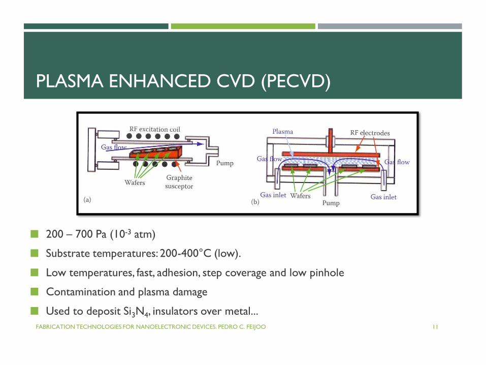
PLASMA ENHANCED CVD (PECVD)
200 – 700 Pa (10-3 atm)
Substrate temperatures: 200-400°C (low).
Low temperatures, fast, adhesion, step coverage and low pinhole
Contamination and plasma damage
Used to deposit Si3N4, insulators over metal...
FABRICATION TECHNOLOGIES FOR NANOELECTRONIC DEVICES. PEDRO C. FEIJOO 11
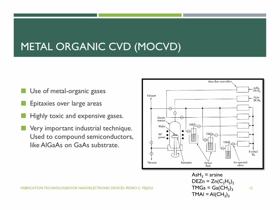
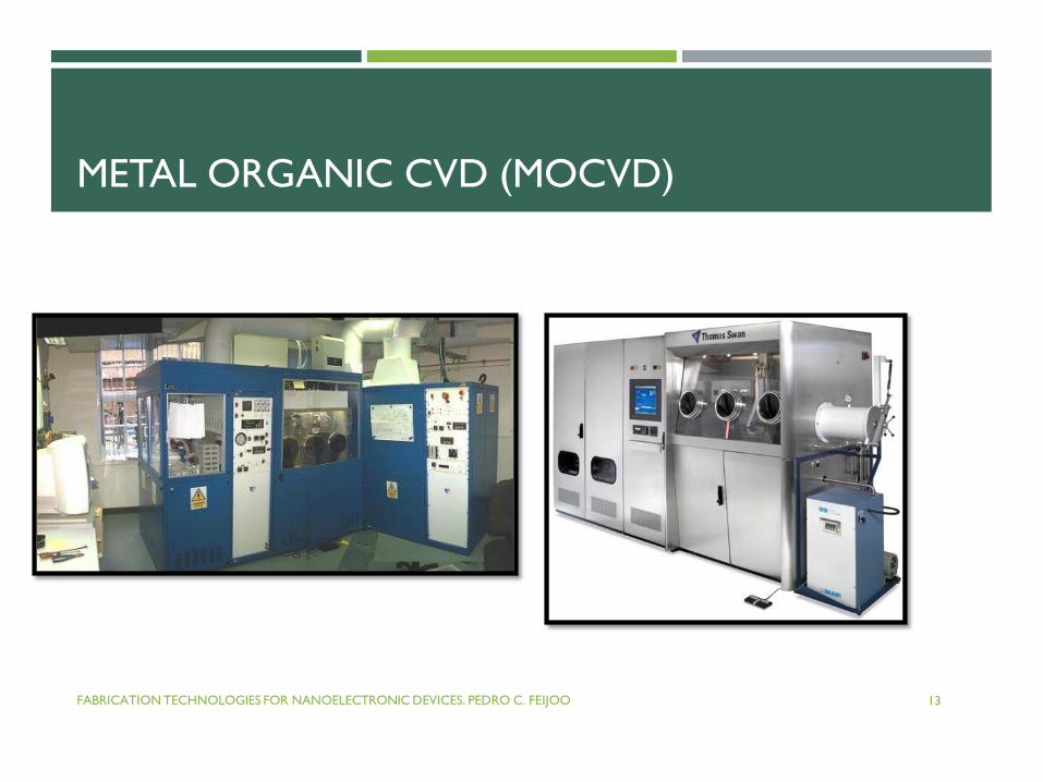
METAL ORGANIC CVD (MOCVD)
Use of metal-organic gases
Epitaxies over large areas
Highly toxic and expensive gases.
Very important industrial technique.
Used to compound semiconductors,
like AlGaAs on GaAs substrate.
FABRICATION TECHNOLOGIES FOR NANOELECTRONIC DEVICES. PEDRO C. FEIJOO 12
AsH3 = arsine
DEZn = Zn(C2H5)2
TMGa = Ga(CH3)3
TMAl = Al(CH3)3
METAL ORGANIC CVD (MOCVD)
MOCVD (2/2)
FABRICATION TECHNOLOGIES FOR NANOELECTRONIC DEVICES. PEDRO C. FEIJOO 13
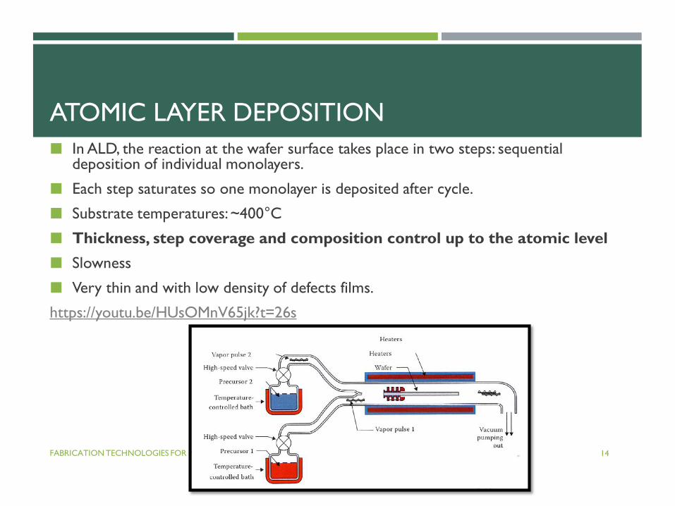
ATOMIC LAYER DEPOSITION
In ALD, the reaction at the wafer surface takes place in two steps: sequential deposition of individual monolayers.
Each step saturates so one monolayer is deposited after cycle.
Substrate temperatures: ~400°C
Thickness, step coverage and composition control up to the atomic level
Slowness
Very thin and with low density of defects films.
https://youtu.be/HUsOMnV65jk?t=26s
FABRICATION TECHNOLOGIES FOR NANOELECTRONIC DEVICES. PEDRO C. FEIJOO 14
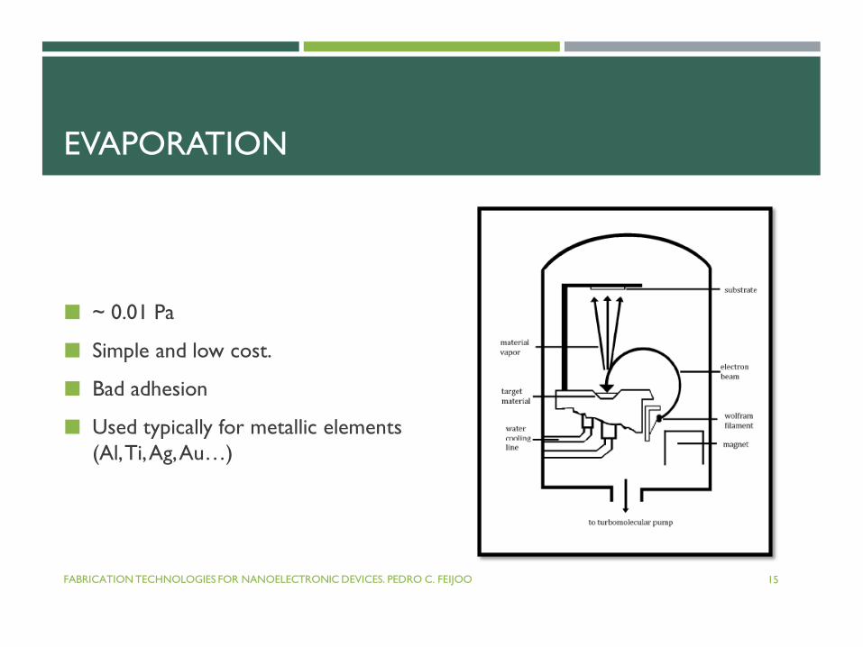
EVAPORATION
~ 0.01 Pa
Simple and low cost.
Bad adhesion
Used typically for metallic elements
(Al, Ti, Ag, Au…)
FABRICATION TECHNOLOGIES FOR NANOELECTRONIC DEVICES. PEDRO C. FEIJOO 15
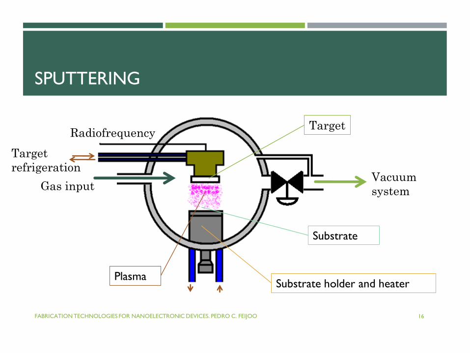
SPUTTERING
FABRICATION TECHNOLOGIES FOR NANOELECTRONIC DEVICES. PEDRO C. FEIJOO 16
Radiofrequency
Target
refrigeration
Gas inputVacuum
system
Target
Substrate
Substrate holder and heaterPlasma
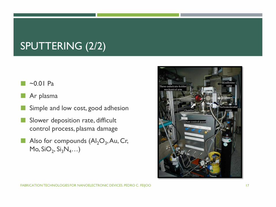
SPUTTERING (2/2)
~0.01 Pa
Ar plasma
Simple and low cost, good adhesion
Slower deposition rate, difficult
control process, plasma damage
Also for compounds (Al2O3, Au, Cr,
Mo, SiO2, Si3N4…)
FABRICATION TECHNOLOGIES FOR NANOELECTRONIC DEVICES. PEDRO C. FEIJOO 17
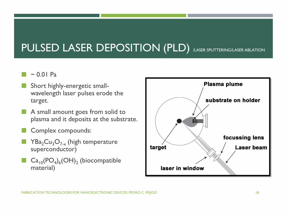
PULSED LASER DEPOSITION (PLD) /LASER SPUTTERING/LASER ABLATION
~ 0.01 Pa
Short highly-energetic small-wavelength laser pulses erode the target.
A small amount goes from solid to plasma and it deposits at the substrate.
Complex compounds:
YBa2Cu3O7-x (high temperature superconductor)
Ca10(PO4)6(OH)2 (biocompatible material)
FABRICATION TECHNOLOGIES FOR NANOELECTRONIC DEVICES. PEDRO C. FEIJOO 18
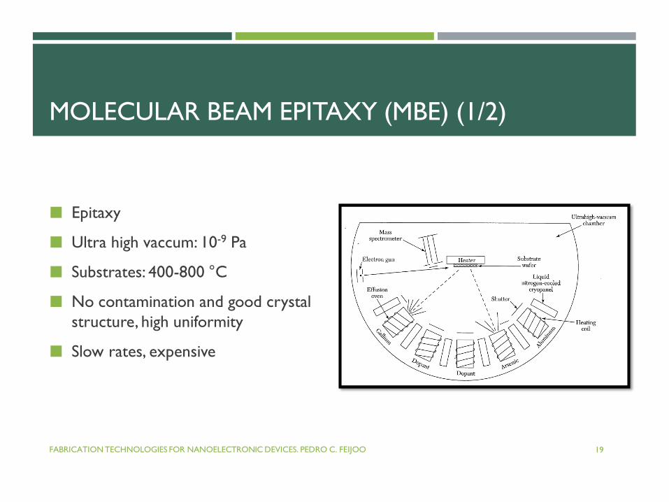
MOLECULAR BEAM EPITAXY (MBE) (1/2)
Epitaxy
Ultra high vaccum: 10-9 Pa
Substrates: 400-800 °C
No contamination and good crystal
structure, high uniformity
Slow rates, expensive
FABRICATION TECHNOLOGIES FOR NANOELECTRONIC DEVICES. PEDRO C. FEIJOO 19
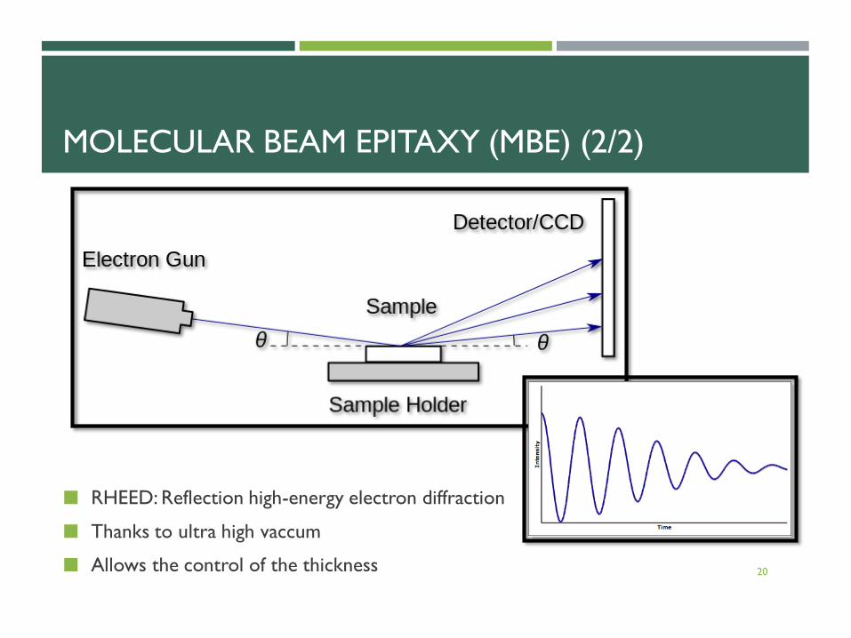
MOLECULAR BEAM EPITAXY (MBE) (2/2)
RHEED: Reflection high-energy electron diffraction
Thanks to ultra high vaccum
Allows the control of the thickness 20
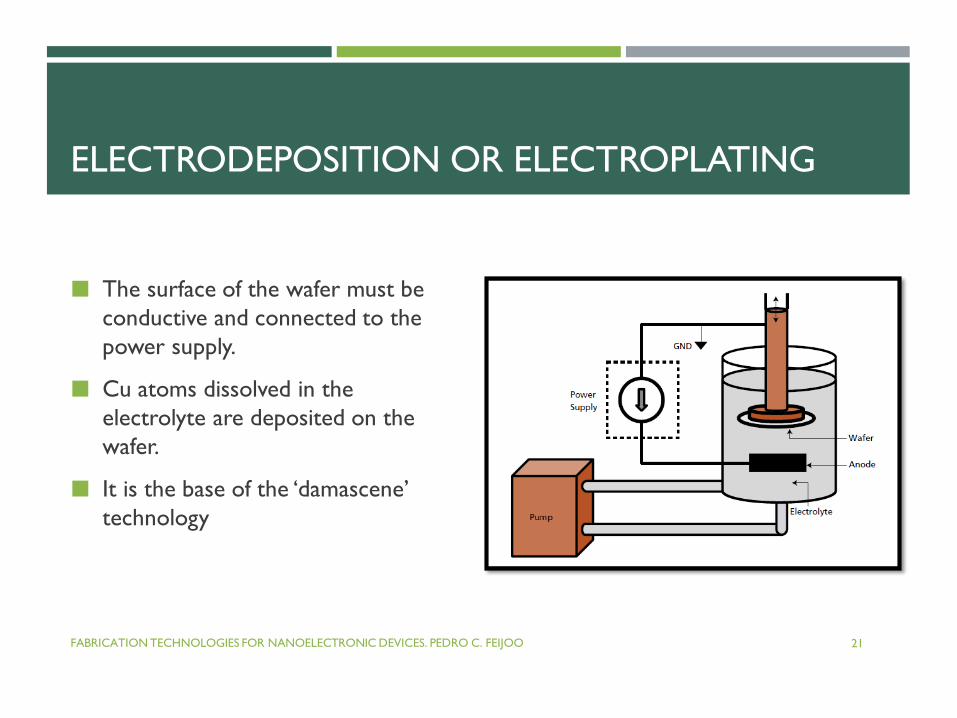
ELECTRODEPOSITION OR ELECTROPLATING
The surface of the wafer must be
conductive and connected to the
power supply.
Cu atoms dissolved in the
electrolyte are deposited on the
wafer.
It is the base of the ‘damascene’
technology
FABRICATION TECHNOLOGIES FOR NANOELECTRONIC DEVICES. PEDRO C. FEIJOO 21
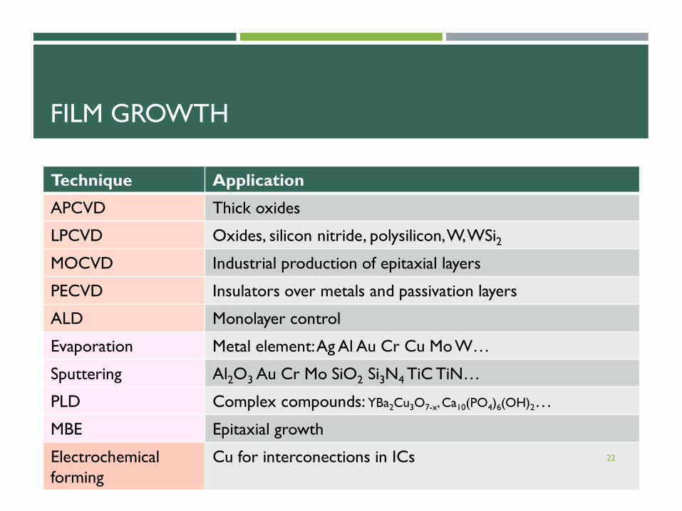
FILM GROWTH
Technique Application
APCVD Thick oxides
LPCVD Oxides, silicon nitride, polysilicon, W, WSi2
MOCVD Industrial production of epitaxial layers
PECVD Insulators over metals and passivation layers
ALD Monolayer control
Evaporation Metal element:Ag Al Au Cr Cu Mo W…
Sputtering Al2O3 Au Cr Mo SiO2 Si3N4 TiC TiN…
PLD Complex compounds: YBa2Cu3O7-x, Ca10(PO4)6(OH)2…
MBE Epitaxial growth
Electrochemical
forming
Cu for interconections in ICs 22
REFERENCES
Fundamentals of microfabrication and nanotechnology, volumen 2: Manufacturing techniques for microfabrication and nanotechnology. 3rd edition. Marc J. Madou. CRC Press 2012. ISBN: 978-1-4200-5519-1
Fundamentals of semiconductor fabrication. Gary S. May and Simon M. Sze. John Wileyand Sons, Inc 2004. ISBN: 0-471-23279-3
Overview of the Use of Copper Interconnects in the Semiconductor Industry. Annabelle Pratt http://www.advanced-energy.com/upload/File/White_Papers/SL-ELECTROPLATING-270-01.pdf
Some figures were extracted from https://en.wikipedia.org
http://www.gan.msm.cam.ac.uk/facilities/mocvd/
http://webstaff.itn.liu.se/~qinzh/MOCVD
http://www.dowcorning.com/content/etronics/etronicschem/etronics_newcvd_tutorial3.asp
FABRICATION TECHNOLOGIES FOR NANOELECTRONIC DEVICES. PEDRO C. FEIJOO 23