reg1117 reg1117a 800ma and 1a low dropout positive regulator 1… · 2017-08-06 · at tj = +25°c,...
TRANSCRIPT

FEATURES FIXED AND ADJUSTABLE VERSIONS 2.85V MODEL FOR SCSI-2 ACTIVE
TERMINATION OUTPUT CURRENT:
REG1117: 800mA maxREG1117A: 1A max
OUTPUT TOLERANCE: 1% max DROPOUT VOLTAGE:
REG1117: 1.2V max at I O = 800mAREG1117A: 1.3V max at I O = 1A
INTERNAL CURRENT LIMIT THERMAL OVERLOAD PROTECTION SOT-223 AND DDPAK SURFACE-MOUNT
PACKAGES
APPLICATIONS SCSI-2 ACTIVE TERMINATION HAND-HELD DATA COLLECTION DEVICES HIGH EFFICIENCY LINEAR REGULATORS BATTERY-POWERED INSTRUMENTATION BATTERY MANAGEMENT CIRCUITS FOR
NOTEBOOK AND PALMTOP PCs CORE VOLTAGE SUPPLY: FPGA, PLD, DSP,
CPU
DESCRIPTIONThe REG1117 is a family of easy-to-use three-terminalvoltage regulators. The family includes a variety of fixed-and adjustable-voltage versions, two currents (800mA and1A) and two package types (SOT-223 and DDPAK). Seethe chart below for available options.
Output voltage of the adjustable versions is set with twoexternal resistors. The REG1117 low dropout voltageallows its use with as little as 1V input-output voltagedifferential.
Laser trimming assures excellent output voltage accuracywithout adjustment. An NPN output stage allows outputstage drive to contribute to the load current for maximumefficiency.
800mA 1A
VOLTAGE SOT-223 DDPAK SOT-223 DDPAK
1.8V
2.5V
2.85V
3.3V
5V
Adjustable
! !
All trademarks are the property of their respective owners.
REG1117REG1117A
SBVS001D − OCTOBER 1992 − REVISED JULY 2004
800mA and 1A Low Dropout Positive Regulator1.8V, 2.5V, 2.85, 3.3V, 5V, and Adjustable
www.ti.com
Copyright 1992−2004, Texas Instruments Incorporated
Please be aware that an important notice concerning availability, standard warranty, and use in critical applications of Texas Instrumentssemiconductor products and disclaimers thereto appears at the end of this data sheet.

"#$$$%"#$$$%
SBVS001D − OCTOBER 1992 − REVISED JULY 2004
www.ti.com
2
ABSOLUTE MAXIMUM RATINGS (1)
Power Dissipation Internally Limited. . . . . . . . . . . . . . . . . . . . . . . . . . Input Voltage +15V. . . . . . . . . . . . . . . . . . . . . . . . . . . . . . . . . . . . . . . Operating Junction Temperature Range −40°C to +125°C. . . . . . . . Storage Temperature Range −65°C to +150°C. . . . . . . . . . . . . . . . . Lead Temperature (soldering, 10s)(2) +300°C. . . . . . . . . . . . . . . . .
(1) Stresses above these ratings may cause permanent damage.(2) See Soldering Methods section.
This integrated circuit can be damaged by ESD. TexasInstruments recommends that all integrated circuits behandled with appropriate precautions. Failure to observe
proper handling and installation procedures can cause damage.
ESD damage can range from subtle performance degradation tocomplete device failure. Precision integrated circuits may be moresusceptible to damage because very small parametric changes couldcause the device not to meet its published specifications.
CONNECTION DIAGRAM
Front View
Plastic SOT−223Plastic DDPAK
Tab is VOUT
VINVOUTGround(Adj.)(1)
Tab isVOUT
VINVOUTGround(Adj.)(1)
NOTE: (1) Adjustable−Voltage Model.

"#$$$%"#$$$%
SBVS001D − OCTOBER 1992 − REVISED JULY 2004
www.ti.com
3
PACKAGE/ORDERING INFORMATION (1)
PRODUCT VO/IO PACKAGE-LEADPACKAGE
DESIGNATOR
OPERATINGTEMPERATURE
RANGE
PACKAGEMARKING
ORDERINGNUMBER
TRANSPORTMEDIA,
QUANTITY
−40°C toREG1117-2.85 Rails, 80
REG1117-2.85 2.85/800mA SOT223-3 DCY−40°C to+125°C BB11172
REG1117-2.85Tape and Reel,
2500
−40°C toREG1117-3.3 Rails, 80
REG1117-3.3 3.3/800mA SOT223-3 DCY−40°C to+125°C BB11174
REG1117-3.3Tape and Reel,
2500
REG1117F-3.3 3.3/800mA DDPAK-3 KTT−40°C to
BB1117F4
REG1117F-3.3KTTTTape and Reel,
50REG1117F-3.3 3.3/800mA DDPAK-3 KTT
−40 C to+125°C BB1117F4
REG1117F-3.3/500Tape and Reel,
500
−40°C toREG1117-5 Rails, 80
REG1117-5 5V/800mA SOT223-3 DCY−40°C to+125°C BB11175
REG1117-5Tape and Reel,
2500
−40°C toREG1117 Rails, 80
REG1117 Adj./800mA SOT223-3 DCY−40°C to+125°C BB1117
REG1117Tape and Reel,
2500
−40°C toREG1117A-1.8 Rails, 80
REG1117A-1.8 1.8V/1A SOT223-3 DCY−40°C to+125°C R111718
REG1117A-1.8Tape and Reel,
2500
REG1117FA-1.8 1.8/1A DDPAK-3 KTT−40°C to
REG1117FA1.8
REG1117FA-1.8KTTTTape and Reel,
50REG1117FA-1.8 1.8/1A DDPAK-3 KTT
−40 C to+125°C REG1117FA1.8
REG1117FA-1.8/500Tape and Reel,
500
−40°C toREG1117A-2.5 Rails, 80
REG1117A-2.5 2.5/1A SOT223-3 DCY−40°C to+125°C R111725
REG1117A-2.5Tape and Reel,
2500
REG1117FA-2.5 2.5/1A DDPAK-3 KTT−40°C to
REG1117FA2.5
REG1117FA-2.5KTTTTape and Reel,
50REG1117FA-2.5 2.5/1A DDPAK-3 KTT
−40 C to+125°C REG1117FA2.5
REG1117FA-2.5/500Tape and Reel,
500
REG1117FA-5 5/1A DDPAK-3 KTT−40°C to
BB1117FA5.0
REG1117FA-5/KTTTTape and Reel,
50REG1117FA-5 5/1A DDPAK-3 KTT
−40 C to+125°C BB1117FA5.0
REG1117FA-5/500Tape and Reel,
500
−40°C toREG1117A Rails, 80
REG1117A Adj./1A SOT223-3 DCY−40°C to+125°C BB1117A
REG1117ATape and Reel,
2500
REG1117FA Adj./1A DDPAK-3 KTT−40°C to
REG1117FA
REG1117FA/KTTTTape and Reel,
50REG1117FA Adj./1A DDPAK-3 KTT
−40 C to+125°C REG1117FA
REG1117FA/500Tape and Reel,
500
(1) For the most current package and ordering information, see the Package Option Addendum located at the end of this data sheet.

"#$$$%"#$$$%
SBVS001D − OCTOBER 1992 − REVISED JULY 2004
www.ti.com
4
ELECTRICAL CHARACTERISTICS At TJ = +25°C, unless otherwise noted.
REG1117, REG1117A
PARAMETER CONDITION MIN TYP MAX UNIT
OUTPUT VOLTAGE
REG1117-2.85 IO = 10mA, VIN = 4.85V 2.820 2.85 2.880 V
See Note 1 IO = 0 to 800mA, VIN = 4.05V to 10V 2.790 2.85 2.910 V
REG1117-3.3 IO = 10mA, VIN = 5.3V 3.270 3.30 3.330 V
See Note 1 IO = 0 to 800mA, VIN = 4.8V to 10V 3.240 3.30 3.360 V
REG1117-5 IO = 10mA, VIN = 7V 4.950 5.00 5.050 V
See Note 1 IO = 0 to 800mA, VIN = 6.5V to 10V 4.900 5.00 5.100 V
REG1117A-1.8 IO = 10mA, VIN = 3.8V 1.782 1.8 1.818 V
See Note 1 IO = 0 to 1A, VIN = 3.8V to 10V 1.764 1.8 1.836 V
REG1117A-2.5 IO = 10mA, VIN = 4.5V 2.475 2.5 2.525 V
See Note 1 IO = 0 to 1A, VIN = 4.5V to 10V 2.450 2.5 2.550 V
REG1117A-5 IO = 10mA, VIN = 7V 4.950 5.0 5.050 V
See Note 1 IO = 0 to 1A, VIN = 7V to 10V 4.900 5.0 5.100 V
REFERENCE VOLTAGE
REG1117 (Adjustable) IO = 10mA, VIN − VO = 2V 1.238 1.250 1.262 V
See Note 1 IO = 10 to 800mA, VIN − VO = 1.4 to 10V 1.225 1.250 1.280 V
REG1117A (Adjustable) IO = 10mA, VIN − VO = 2V 1.238 1.250 1.262 V
See Note 1 IO = 10mA to 1A, VIN − VO = 1.4 to 10V 1.225 1.250 1.280 V
LINE REGULATION
REG1117-2.85(1) IO = 0, VIN = 4.25 to 10V 1 7 mV
REG1117-3.3(1) IO = 0, VIN = 4.8 to 10V 2 7 mV
REG1117-5(1) IO = 0, VIN = 6.5 to 15V 3 10 mV
REG1117 (Adjustable)(1) IO = 10mA, VIN − VO = 1.5 to 13.75V 0.1 0.4 %
REG1117A (Adjustable)(1) IO = 10mA, VIN − VO = 1.5 to 13.75V 0.1 0.4 %
REG1117A-1.8(1) IO = 0, VIN = 3.8V to 10V 1 7 mV
REG1117A-2.5(1) IO = 0, VIN = 4.5V to 10V 1 7 mV
REG1117A-5.0(1) IO = 0, VIN = 7V to 15V 3 10 mV
LOAD REGULATION
REG1117-2.85(1) IO = 0 to 800mA, VIN = 4.25V 2 10 mV
REG1117-3.3(1) IO = 0 to 800mA, VIN = 4.8V 3 12 mV
REG1117-5(1) IO = 0 to 800mA, VIN = 6.5V 3 15 mV
REG1117 (Adjustable)(1)(2) IO = 10 to 800mA, VIN − VO = 3V 0.1 0.4 %
REG1117A (Adjustable)(1)(2) IO = 10mA to 1A, VIN − VO = 3V 0.1 0.4 %
REG1117A-1.8(1) IO = 0 to 1A, VIN = 3.8V 2 10 mV
REG1117A-2.5 IO = 0 to 1A, VIN = 4.5V 2 10 mV
REG1117A-5 IO = 0 to 1A, VIN = 7.0V 3 15 mV
DROPOUT VOLTAGE(3)
All Models(1) IO = 100mA 1.00 1.10 V
See Note 1 IO = 500mA 1.05 1.15 V
REG1117 Models(1) IO = 800mA 1.10 1.20 V
REG1117A IO = 1A 1.2 1.30 V
See Note 1 IO = 1A 1.2 1.55 V
(1) Specification applies over the full specified junction temperature range, 0°C to +125°C.(2) REG1117 and REG1117A adjustable versions require a minimum load current for ±3% regulation.(3) Dropout voltage is the input voltage minus output voltage that produces a 1% decrease in output voltage.(4) Percentage change in unloaded output voltage before versus after a 30ms power pulse of IO = 800mA (REG1117 models), IO = 1A (REG1117A),
VIN − VO = 1.4V (reading taken 10ms after pulse).

"#$$$%"#$$$%
SBVS001D − OCTOBER 1992 − REVISED JULY 2004
www.ti.com
5
ELECTRICAL CHARACTERISTICS (continued)At TJ = +25°C, unless otherwise noted.
REG1117, REG1117A
PARAMETER UNITMAXTYPMINCONDITION
CURRENT LIMIT
REG1117 Models VIN − VO = 5V 800 950 1200 mA
REG1117A VIN − VO = 5V 1000 1250 1600 mA
MINIMUM LOAD CURRENT
Adjustable Models(1)(2) VIN − VO = 13.75V 1.7 5 mA
QUIESCENT CURRENT
Fixed-Voltage Models(1) VIN − VO = 5V 4 10 mA
ADJUSTABLE PIN CURRENT(1)(2) IO = 10mA, VIN − VO = 1.4 to 10V 50 120 µA
vs Load Current, REG1117(1) IO = 10mA to 800mA, VIN − VO = 1.4 to 10V 0.5 5 µA
vs Load Current, REG1117A(1) IO = 10mA to 1A, VIN − VO = 1.4 to 10V 0.5 5 µA
THERMAL REGULATION
All Models(4) 30ms Pulse 0.01 0.1 %/W
RIPPLE REJECTION
All Models f = 120Hz, VIN − VOUT = 3V + 1VPP Ripple 62 dB
TEMPERATURE DRIFT
Fixed-Voltage Models TJ = 0°C to +125°C 0.5 %
Adjustable Models TJ = 0°C to +125°C 2 %
LONG-TERM STABILITY
All Models TA = 125°C, 1000Hr 0.3 %
OUTPUT NOISE
rms Noise, All Models f = 10Hz to 10kHz 0.003 %
THERMAL RESISTANCE
Thermal Resistance, JC (Junction-to-Case at Tab)
3-Lead SOT-223 Surface-Mount 15 °C/W
3-Lead DDPAK Surface-Mount f > 50Hz 2 °C/W
dc 3 °C/W
Thermal Resistance, JA (Junction-to-Case at Tab)
3-Lead DDPAK Surface-Mount No Heatsink 65 °C/W
(1) Specification applies over the full specified junction temperature range, 0°C to +125°C.(2) REG1117 and REG1117A adjustable versions require a minimum load current for ±3% regulation.(3) Dropout voltage is the input voltage minus output voltage that produces a 1% decrease in output voltage.(4) Percentage change in unloaded output voltage before versus after a 30ms power pulse of IO = 800mA (REG1117 models), IO = 1A (REG1117A),
VIN − VO = 1.4V (reading taken 10ms after pulse).

"#$$$%"#$$$%
SBVS001D − OCTOBER 1992 − REVISED JULY 2004
www.ti.com
6
SIMPLIFIED SCHEMATIC
ThermalLimit
10XVOUT
VIN
Ground (Fixed−voltage Models)
Adj. (Adjustable−voltage Model)
(Substrate)
+
CurrentLimit

"#$$$%"#$$$%
SBVS001D − OCTOBER 1992 − REVISED JULY 2004
www.ti.com
7
TYPICAL CHARACTERISTICS
At TA = +25°C, all models, unless otherwise noted.
SHORT−CIRCUIT CURRENT vs TEMPERATURE1400
1300
1200
1100
1000
900
800−50 −25 0 25 50 75 100
Temperature (C)
Sh
ort−
Cir
cuit
Cu
rren
t(m
A)
REG1117A
REG1117 Models
LOAD REGULATION( ∆ILOAD = 800mA)
1
0
1
−2
−3
−4
−5
−6
−7−50 −25 0 25 50 75 100
Temperature (C)
Ou
tput
Vol
tage
Dev
iatio
n(m
V)
REG1117−2.85
REG1117A−1.8
REG1117−5
LINE REGULATION vs TEMPERATURE6
5
4
3
2
1
0
−1
−2−50 −25 0 25 50 75 100
Temperature (C)
Ou
tput
Vo
ltage
Cha
nge
(mV
)
REG1117A−1.8VIN = 3.8V to 10V
VIN = 6.5V to 15VREG1117−5
RIPPLE REJECTION vs FREQUENCY
Frequency (Hz)
Rip
ple
Re
ject
ion
(dB
)100
90
80
70
60
50
40
30
20
10
010 100 1k 10k 100k
IOUT = 100mAVRIPPLE = 1.0VPP
OUTPUT VOLTAGE vs TEMPERATURE2.0
1.0
0
−1.0
−2.0−50 −25 0 25 50 75 100
Temperature (C)
Out
putV
olta
ge
Cha
nge
(%)
IO = 10mA
QUIESCENT CURRENT vs TEMPERATURE8
7
6
5
4
3
2
1
0−50 −25 0 25 50 75 100
Temperature (C)
Qui
esce
ntC
urr
ent
(mA
)
Fixed−Voltage Models

"#$$$%"#$$$%
SBVS001D − OCTOBER 1992 − REVISED JULY 2004
www.ti.com
8
TYPICAL CHARACTERISTICS (continued)At TA = +25°C, all models, unless otherwise noted.
LOAD TRANSIENT RESPONSE
0.1
0
−0.1
0.5
0
−0.5
Load
Cur
rent
(A)
Out
putV
olta
geD
evia
tions
(V)
0 20 40 60 80 100
Time (µs)
CIN = 10µFCOUT = 10µFTantalumVIN = 4.25VPreload = 0.1A
LINE TRANSIENT RESPONSE60
40
20
0
−20
−40
5.25
4.25
3.25Inpu
tVol
tage
(V)
Out
putV
olta
geD
evia
tion
(mV
)
0 20 40 60 80 100 120 140 160 180 200
Time (µs)
CIN = 1µFCOUT = 10µF TantalumIOUT = 0.1A
APPLICATIONS INFORMATIONFigure 1 shows the basic hookup diagram for fixed-voltagemodels. All models require an output capacitor for properoperation, and for improving high-frequency loadregulation; a 10µF tantalum capacitor is recommended.Aluminum electrolytic types of 50µF or greater can also beused. A high-quality capacitor should be used to assurethat the ESR (Effective Series Resistance) is less than0.5Ω.
REG1117 VOVIN
10µFTantalum
10µFTantalum
+ +
Figure 1. Fixed-Voltage Model—BasicConnections
Figure 2 shows a hookup diagram for the adjustablevoltage model. Resistor values are shown for somecommonly-used output voltages. Values for other voltagescan be calculated from the equation shown in Figure 2. Forbest load regulation, connect R1 close to the output pin andR2 close to the ground side of the load as shown.
THERMAL CONSIDERATIONSThe REG1117 has current limit and thermal shutdowncircuits that protect it from overload. The thermal shutdownactivates at approximately TJ = 165°C. For continuousoperation, however, the junction temperature should notbe allowed to exceed 125°C. Any tendency to activate thethermal shutdown in normal use is an indication of aninadequate heat sink or excessive power dissipation. Thepower dissipation is equal to:
PD = (VIN – VOUT) IOUT
The junction temperature can be calculated by:
TJ = TA + PD (JA)
where TA is the ambient temperature, and JA is thejunction-to-ambient thermal resistance.
REG1117(Adj)
VIN VO
C210µF
C110µF
C3(1)
10µF
+ +
+
R1
R2
Load
3 2
1
NOTES: (1) C3 optional. Improves high−frequency line rejection. (2) Resistors are standard 1% values.
VO = x (1.25V) + (50µA) (R2)R1
R1 + R2
This term is negligible withproper choice of values−seetable at right.
VOUT R1 R2(V) (Ω)(2) (Ω)(2)
1.25 Open Short1.5 750 1472.1 158 107
2.85 169 2153 137 191
3.3 115 1875 113 34010 113 787
Figure 2. Adjustable-Voltage Model—Basic Connections

"#$$$%"#$$$%
SBVS001D − OCTOBER 1992 − REVISED JULY 2004
www.ti.com
9
A simple experiment will determine whether the maximumrecommended junction temperature is exceeded in anactual circuit board and mounting configuration: Increasethe ambient temperature above that expected in normaloperation until the device’s thermal shutdown is activated.If this occurs at more than 40°C above the maximumexpected ambient temperature, then TJ will be less than125°C during normal operation.
The internal protection circuitry of the REG1117 wasdesigned to protect against overload conditions. It was notintended to replace proper heat sinking. Continuouslyrunning the REG1117 into thermal shutdown will degradereliability.
LAYOUT CONSIDERATIONSThe DDPAK (REG1117F-3.3 and REG1117FA) is asurface-mount power package that has excellent thermalcharacteristics. For best thermal performance, themounting tab should be soldered directly to a circuit boardcopper area, as shown in Figure 3. Increasing the copperarea improves heat dissipation. Figure 4 shows typicalthermal resistance from junction-to-ambient as a functionof the copper area.
3−Lead DDPAK(1)
NOTE: (1) For improved thermal performance increasefootprint area. See Figure 4 (Thermal Resistance vsCircuit Board Copper Area).
All measurementsin inches.
0.45
0.08
5
0.2
0.51
0.10
0.155 0.05
Figure 3. DDPAK Footprint
THERMAL RESISTANCE vsCIRCUIT BOARD COPPER AREA
60
50
40
30
20
100 1 2 3 4 5
Copper Area (inches2)
REG1117FDDPAK Surface Mount Package
1oz copper
The
rmal
Res
ista
nce,
JA
(°C
/W)
Circuit Board Copper Area
REG1117FDDPAK Surface−Mount Package
Figure 4. DDPAK Thermal Resistance versus Circuit Board Copper Area

"#$$$%"#$$$%
SBVS001D − OCTOBER 1992 − REVISED JULY 2004
www.ti.com
10
The SOT-223 package derives heat sinking fromconduction through its copper leads, especially the largemounting tab. These must be soldered to a circuit boardwith a substantial amount of copper remaining, as shownin Figure 5. Circuit board traces connecting the tab and theleads should be made as large as practical. The mountingtab of both packages is electrically connected to VOUT.
Total Area: 50 x 50mm
35 x 17 mm
16 x 10 mm 16 x 10 mm
Without backside copper: JA ≈ 59C/W
With solid backside copper: JA ≈ 49C/W
Figure 5. SOT-223 Circuit Board Layout Example
Other nearby circuit traces, including those on the backside of the circuit board, help conduct heat away from thedevice, even though they may not be electricallyconnected. Make all nearby copper traces as wide aspossible and leave only narrow gaps between traces.
Table 1 shows approximate values of JA for various circuitboard and copper areas for the SOT-223 package. Nearbyheat dissipating components, circuit board mountingconditions, and ventilation can dramatically affect theactual JA. Proper heat sinking significantly increases themaximum power dissipation at a given ambienttemperature, as shown in Figure 6.
Table 1. SOT-223 JA for Various BoardConfigurations
(1)
SOT-223THERMAL
TOTAL PCBOARD
TOPSIDE(1)COPPER
BACKSIDECOPPER
THERMALRESISTANCEJUNCTION-BOARD
AREACOPPER
AREACOPPER
AREAJUNCTION-
TO-AMBIENT
2500mm2 2500mm2 2500mm2 46°C/W
2500mm2 1250mm2 2500mm2 47°C/W
2500mm2 950mm2 2500mm2 49°C/W
2500mm2 2500mm2 0 51°C/W
2500mm2 1800mm2 0 53°C/W
1600mm2 600mm2 1600mm2 55°C/W
2500mm2 1250mm2 0 58°C/W
2500mm2 915mm2 0 59°C/W
1600mm2 600mm2 0 67°C/W
900mm2 340mm2 900mm2 72°C/W
900mm2 340mm2 0 85°C/W
(1) Tab is attached to the topside copper.
SOLDERING METHODS
Both REG1117 packages are suitable for infrared reflowand vapor-phase reflow soldering techniques. The highrate of temperature change that occurs with wavesoldering or hand soldering can damage the REG1117.
INSPEC Abstract Number: B91007604, C91012627.Kelly, E.G. “Thermal Characteristics of Surface 5WK9ΩPackages.” The Proceedings of SMTCON. Surface MountTechnology Conference and Exposition: CompetitiveSurface Mount Technology, April 3−6, 1990, Atlantic City,NJ, USA. Abstract Publisher: IC Manage, 1990, Chicago,IL, USA.
6
5
4
3
2
1
0
Pow
er
Dis
sip
atio
n(W
atts
)
0 25 50 75 100 125
Ambient Temperature (C)
MAXIMUM POWER DISSIPATIONvs AMBIENT TEMPERATURE
PD = (TJ (max) − TA) / JA
TJ (max) = 150C
DDPAKSOT−223
JA = 85C/W(340mm2 topside copper,no backside copper)
JA = 46C/W(2500mm2 topside andbackside copper)
JA = 27C/W(4in2 one oz coppermounting pad)
JA = 65C/W(no heat sink)
Figure 6. Maximum Power Dissipation versus Ambient Temperature

"#$$$%"#$$$%
SBVS001D − OCTOBER 1992 − REVISED JULY 2004
www.ti.com
11
10µF10µF
REG1117−2.85110Ω110Ω
110Ω110Ω
10µF 10µF
1N5817
5VTERMPWR
2.85V 2.85V
TERMPWR
1N5817
5V
(Up to 27 Lines)
REG1117−2.85
Figure 7. SCSI Active Termination Configuration
REG1117−5
GND
In Out
10µF 100µF+ +
5V to 10V
10µF+
VIN > 12V
1kΩ
Figure 8. Adjusting Output of Fixed Voltage Models
REG1117−5
GND
In Out
10µF 100µF+ +
7.5VVIN > 9.0V
2.5VOUT
REF1004−2.5
Figure 9. Regulator with Reference
REG1117−5
GND
In Out
REG1117−5
GND
In Out
10µF
10µF
100µF6.5V
1kΩ
50Ω
5.2V Line5.0V Battery
VIN
+
+ +
Figure 10. Battery Backed-Up Regulated Supply
REG1117−5
GND
In Out
10µF 100µF+ +
VOUT = −5V
VIN
Floating Input
Figure 11. Low Dropout Negative Supply

PACKAGE OPTION ADDENDUM
www.ti.com 17-Mar-2017
Addendum-Page 1
PACKAGING INFORMATION
Orderable Device Status(1)
Package Type PackageDrawing
Pins PackageQty
Eco Plan(2)
Lead/Ball Finish(6)
MSL Peak Temp(3)
Op Temp (°C) Device Marking(4/5)
Samples
REG1117 ACTIVE SOT-223 DCY 4 80 Green (RoHS& no Sb/Br)
CU NIPDAU Level-1-260C-UNLIM 0 to 125 BB1117
REG1117-2.85 ACTIVE SOT-223 DCY 4 80 Green (RoHS& no Sb/Br)
CU NIPDAU Level-1-260C-UNLIM 0 to 125 BB11172
REG1117-2.85/2K5 ACTIVE SOT-223 DCY 4 2500 Green (RoHS& no Sb/Br)
CU NIPDAU Level-1-260C-UNLIM 0 to 125 BB11172
REG1117-2.85G4 ACTIVE SOT-223 DCY 4 80 Green (RoHS& no Sb/Br)
CU NIPDAU Level-1-260C-UNLIM 0 to 125 BB11172
REG1117-3.3 ACTIVE SOT-223 DCY 4 80 Green (RoHS& no Sb/Br)
CU NIPDAU Level-1-260C-UNLIM 0 to 125 BB11174
REG1117-3.3/2K5 ACTIVE SOT-223 DCY 4 2500 Green (RoHS& no Sb/Br)
CU NIPDAU Level-1-260C-UNLIM 0 to 125 BB11174
REG1117-3.3/2K5G4 ACTIVE SOT-223 DCY 4 2500 Green (RoHS& no Sb/Br)
CU NIPDAU Level-1-260C-UNLIM 0 to 125 BB11174
REG1117-3.3G4 ACTIVE SOT-223 DCY 4 80 Green (RoHS& no Sb/Br)
CU NIPDAU Level-1-260C-UNLIM 0 to 125 BB11174
REG1117-5 ACTIVE SOT-223 DCY 4 80 Green (RoHS& no Sb/Br)
CU NIPDAU Level-1-260C-UNLIM 0 to 125 BB11175
REG1117-5/2K5 ACTIVE SOT-223 DCY 4 2500 Green (RoHS& no Sb/Br)
CU NIPDAU Level-1-260C-UNLIM 0 to 125 BB11175
REG1117-5G4 ACTIVE SOT-223 DCY 4 80 Green (RoHS& no Sb/Br)
CU NIPDAU Level-1-260C-UNLIM 0 to 125 BB11175
REG1117/2K5 ACTIVE SOT-223 DCY 4 2500 Green (RoHS& no Sb/Br)
CU NIPDAU Level-1-260C-UNLIM 0 to 125 BB1117
REG1117/2K5G4 ACTIVE SOT-223 DCY 4 2500 Green (RoHS& no Sb/Br)
CU NIPDAU Level-1-260C-UNLIM 0 to 125 BB1117
REG1117A ACTIVE SOT-223 DCY 4 80 Green (RoHS& no Sb/Br)
CU NIPDAU Level-1-260C-UNLIM 0 to 125 BB1117A
REG1117A-1.8 ACTIVE SOT-223 DCY 4 80 Green (RoHS& no Sb/Br)
CU NIPDAU Level-1-260C-UNLIM 0 to 125 R111718
REG1117A-1.8/2K5 ACTIVE SOT-223 DCY 4 2500 Green (RoHS& no Sb/Br)
CU NIPDAU Level-1-260C-UNLIM 0 to 125 R111718
REG1117A-1.8G4 ACTIVE SOT-223 DCY 4 80 Green (RoHS& no Sb/Br)
CU NIPDAU Level-1-260C-UNLIM 0 to 125 R111718

PACKAGE OPTION ADDENDUM
www.ti.com 17-Mar-2017
Addendum-Page 2
Orderable Device Status(1)
Package Type PackageDrawing
Pins PackageQty
Eco Plan(2)
Lead/Ball Finish(6)
MSL Peak Temp(3)
Op Temp (°C) Device Marking(4/5)
Samples
REG1117A-2.5 ACTIVE SOT-223 DCY 4 80 Green (RoHS& no Sb/Br)
CU NIPDAU Level-1-260C-UNLIM 0 to 125 R111725
REG1117A-2.5/2K5 ACTIVE SOT-223 DCY 4 2500 Green (RoHS& no Sb/Br)
CU NIPDAU Level-1-260C-UNLIM 0 to 125 R111725
REG1117A-2.5G4 ACTIVE SOT-223 DCY 4 80 Green (RoHS& no Sb/Br)
CU NIPDAU Level-1-260C-UNLIM 0 to 125 R111725
REG1117A/2K5 ACTIVE SOT-223 DCY 4 2500 Green (RoHS& no Sb/Br)
CU NIPDAU Level-1-260C-UNLIM 0 to 125 BB1117A
REG1117A/2K5G4 ACTIVE SOT-223 DCY 4 2500 Green (RoHS& no Sb/Br)
CU NIPDAU Level-1-260C-UNLIM 0 to 125 BB1117A
REG1117AG4 ACTIVE SOT-223 DCY 4 80 Green (RoHS& no Sb/Br)
CU NIPDAU Level-1-260C-UNLIM 0 to 125 BB1117A
REG1117F-3.3/500 ACTIVE DDPAK/TO-263
KTT 3 500 Green (RoHS& no Sb/Br)
CU SN Level-2-260C-1 YEAR 0 to 125 REG1117F4
REG1117F-3.3KTTT ACTIVE DDPAK/TO-263
KTT 3 50 Green (RoHS& no Sb/Br)
CU SN Level-2-260C-1 YEAR 0 to 125 REG1117F4
REG1117F33KTTTG3 ACTIVE DDPAK/TO-263
KTT 3 50 Green (RoHS& no Sb/Br)
CU SN Level-2-260C-1 YEAR 0 to 125 REG1117F4
REG1117FA-1.8KTTT ACTIVE DDPAK/TO-263
KTT 3 50 Green (RoHS& no Sb/Br)
CU SN Level-2-260C-1 YEAR 0 to 125 REG1117FA1.8
REG1117FA-2.5/500 ACTIVE DDPAK/TO-263
KTT 3 500 Green (RoHS& no Sb/Br)
CU SN Level-2-260C-1 YEAR 0 to 125 REG1117FA2.5
REG1117FA-2.5KTTT ACTIVE DDPAK/TO-263
KTT 3 50 Green (RoHS& no Sb/Br)
CU SN Level-2-260C-1 YEAR 0 to 125 REG1117FA2.5
REG1117FA-5.0/500 ACTIVE DDPAK/TO-263
KTT 3 500 Green (RoHS& no Sb/Br)
CU SN Level-2-260C-1 YEAR 0 to 125 REG1117FA5.0
REG1117FA-5.0KTTT ACTIVE DDPAK/TO-263
KTT 3 50 Green (RoHS& no Sb/Br)
CU SN Level-2-260C-1 YEAR 0 to 125 REG1117FA5.0
REG1117FA-5.0KTTTG ACTIVE DDPAK/TO-263
KTT 3 50 Green (RoHS& no Sb/Br)
CU SN Level-2-260C-1 YEAR 0 to 125 REG1117FA5.0
REG1117FA/500 ACTIVE DDPAK/TO-263
KTT 3 500 Green (RoHS& no Sb/Br)
CU SN Level-2-260C-1 YEAR 0 to 125 REG1117FA
REG1117FA1.8KTTTG3 ACTIVE DDPAK/TO-263
KTT 3 50 Green (RoHS& no Sb/Br)
CU SN Level-2-260C-1 YEAR 0 to 125 REG1117FA1.8
REG1117FA2.5KTTTG3 ACTIVE DDPAK/TO-263
KTT 3 50 Green (RoHS& no Sb/Br)
CU SN Level-2-260C-1 YEAR 0 to 125 REG1117FA2.5

PACKAGE OPTION ADDENDUM
www.ti.com 17-Mar-2017
Addendum-Page 3
Orderable Device Status(1)
Package Type PackageDrawing
Pins PackageQty
Eco Plan(2)
Lead/Ball Finish(6)
MSL Peak Temp(3)
Op Temp (°C) Device Marking(4/5)
Samples
REG1117FAKTTT ACTIVE DDPAK/TO-263
KTT 3 50 Green (RoHS& no Sb/Br)
CU SN Level-2-260C-1 YEAR 0 to 125 REG1117FA
REG1117G4 ACTIVE SOT-223 DCY 4 80 Green (RoHS& no Sb/Br)
CU NIPDAU Level-1-260C-UNLIM 0 to 125 BB1117
(1) The marketing status values are defined as follows:ACTIVE: Product device recommended for new designs.LIFEBUY: TI has announced that the device will be discontinued, and a lifetime-buy period is in effect.NRND: Not recommended for new designs. Device is in production to support existing customers, but TI does not recommend using this part in a new design.PREVIEW: Device has been announced but is not in production. Samples may or may not be available.OBSOLETE: TI has discontinued the production of the device.
(2) Eco Plan - The planned eco-friendly classification: Pb-Free (RoHS), Pb-Free (RoHS Exempt), or Green (RoHS & no Sb/Br) - please check http://www.ti.com/productcontent for the latest availabilityinformation and additional product content details.TBD: The Pb-Free/Green conversion plan has not been defined.Pb-Free (RoHS): TI's terms "Lead-Free" or "Pb-Free" mean semiconductor products that are compatible with the current RoHS requirements for all 6 substances, including the requirement thatlead not exceed 0.1% by weight in homogeneous materials. Where designed to be soldered at high temperatures, TI Pb-Free products are suitable for use in specified lead-free processes.Pb-Free (RoHS Exempt): This component has a RoHS exemption for either 1) lead-based flip-chip solder bumps used between the die and package, or 2) lead-based die adhesive used betweenthe die and leadframe. The component is otherwise considered Pb-Free (RoHS compatible) as defined above.Green (RoHS & no Sb/Br): TI defines "Green" to mean Pb-Free (RoHS compatible), and free of Bromine (Br) and Antimony (Sb) based flame retardants (Br or Sb do not exceed 0.1% by weightin homogeneous material)
(3) MSL, Peak Temp. - The Moisture Sensitivity Level rating according to the JEDEC industry standard classifications, and peak solder temperature.
(4) There may be additional marking, which relates to the logo, the lot trace code information, or the environmental category on the device.
(5) Multiple Device Markings will be inside parentheses. Only one Device Marking contained in parentheses and separated by a "~" will appear on a device. If a line is indented then it is a continuationof the previous line and the two combined represent the entire Device Marking for that device.
(6) Lead/Ball Finish - Orderable Devices may have multiple material finish options. Finish options are separated by a vertical ruled line. Lead/Ball Finish values may wrap to two lines if the finishvalue exceeds the maximum column width.
Important Information and Disclaimer:The information provided on this page represents TI's knowledge and belief as of the date that it is provided. TI bases its knowledge and belief on informationprovided by third parties, and makes no representation or warranty as to the accuracy of such information. Efforts are underway to better integrate information from third parties. TI has taken andcontinues to take reasonable steps to provide representative and accurate information but may not have conducted destructive testing or chemical analysis on incoming materials and chemicals.TI and TI suppliers consider certain information to be proprietary, and thus CAS numbers and other limited information may not be available for release.
In no event shall TI's liability arising out of such information exceed the total purchase price of the TI part(s) at issue in this document sold by TI to Customer on an annual basis.
PACKAGE OPTION ADDENDUM
www.ti.com 17-Mar-2017
Addendum-Page 4

TAPE AND REEL INFORMATION
*All dimensions are nominal
Device PackageType
PackageDrawing
Pins SPQ ReelDiameter
(mm)
ReelWidth
W1 (mm)
A0(mm)
B0(mm)
K0(mm)
P1(mm)
W(mm)
Pin1Quadrant
REG1117-2.85/2K5 SOT-223 DCY 4 2500 330.0 12.4 7.1 7.45 1.88 8.0 12.0 Q3
REG1117-3.3/2K5 SOT-223 DCY 4 2500 330.0 12.4 7.1 7.45 1.88 8.0 12.0 Q3
REG1117-5/2K5 SOT-223 DCY 4 2500 330.0 12.4 7.1 7.45 1.88 8.0 12.0 Q3
REG1117/2K5 SOT-223 DCY 4 2500 330.0 12.4 7.1 7.45 1.88 8.0 12.0 Q3
REG1117A-1.8/2K5 SOT-223 DCY 4 2500 330.0 12.4 7.1 7.45 1.88 8.0 12.0 Q3
REG1117A-2.5/2K5 SOT-223 DCY 4 2500 330.0 12.4 7.1 7.45 1.88 8.0 12.0 Q3
REG1117A/2K5 SOT-223 DCY 4 2500 330.0 12.4 7.1 7.45 1.88 8.0 12.0 Q3
REG1117F-3.3/500 DDPAK/TO-263
KTT 3 500 330.0 24.4 10.6 15.6 4.9 16.0 24.0 Q2
REG1117F-3.3KTTT DDPAK/TO-263
KTT 3 50 330.0 24.4 10.6 15.6 4.9 16.0 24.0 Q2
REG1117FA-1.8KTTT DDPAK/TO-263
KTT 3 50 330.0 24.4 10.6 15.6 4.9 16.0 24.0 Q2
REG1117FA-2.5/500 DDPAK/TO-263
KTT 3 500 330.0 24.4 10.6 15.6 4.9 16.0 24.0 Q2
REG1117FA-2.5KTTT DDPAK/TO-263
KTT 3 50 330.0 24.4 10.6 15.6 4.9 16.0 24.0 Q2
REG1117FA-5.0/500 DDPAK/TO-263
KTT 3 500 330.0 24.4 10.6 15.6 4.9 16.0 24.0 Q2
REG1117FA-5.0KTTT DDPAK/ KTT 3 50 330.0 24.4 10.6 15.6 4.9 16.0 24.0 Q2
PACKAGE MATERIALS INFORMATION
www.ti.com 5-Aug-2017
Pack Materials-Page 1

Device PackageType
PackageDrawing
Pins SPQ ReelDiameter
(mm)
ReelWidth
W1 (mm)
A0(mm)
B0(mm)
K0(mm)
P1(mm)
W(mm)
Pin1Quadrant
TO-263
REG1117FA/500 DDPAK/TO-263
KTT 3 500 330.0 24.4 10.6 15.6 4.9 16.0 24.0 Q2
REG1117FAKTTT DDPAK/TO-263
KTT 3 50 330.0 24.4 10.6 15.6 4.9 16.0 24.0 Q2
*All dimensions are nominal
Device Package Type Package Drawing Pins SPQ Length (mm) Width (mm) Height (mm)
REG1117-2.85/2K5 SOT-223 DCY 4 2500 358.0 335.0 35.0
REG1117-3.3/2K5 SOT-223 DCY 4 2500 358.0 335.0 35.0
REG1117-5/2K5 SOT-223 DCY 4 2500 358.0 335.0 35.0
REG1117/2K5 SOT-223 DCY 4 2500 358.0 335.0 35.0
REG1117A-1.8/2K5 SOT-223 DCY 4 2500 358.0 335.0 35.0
REG1117A-2.5/2K5 SOT-223 DCY 4 2500 358.0 335.0 35.0
REG1117A/2K5 SOT-223 DCY 4 2500 358.0 335.0 35.0
REG1117F-3.3/500 DDPAK/TO-263 KTT 3 500 367.0 367.0 45.0
REG1117F-3.3KTTT DDPAK/TO-263 KTT 3 50 367.0 367.0 45.0
REG1117FA-1.8KTTT DDPAK/TO-263 KTT 3 50 367.0 367.0 45.0
REG1117FA-2.5/500 DDPAK/TO-263 KTT 3 500 367.0 367.0 45.0
REG1117FA-2.5KTTT DDPAK/TO-263 KTT 3 50 367.0 367.0 45.0
PACKAGE MATERIALS INFORMATION
www.ti.com 5-Aug-2017
Pack Materials-Page 2
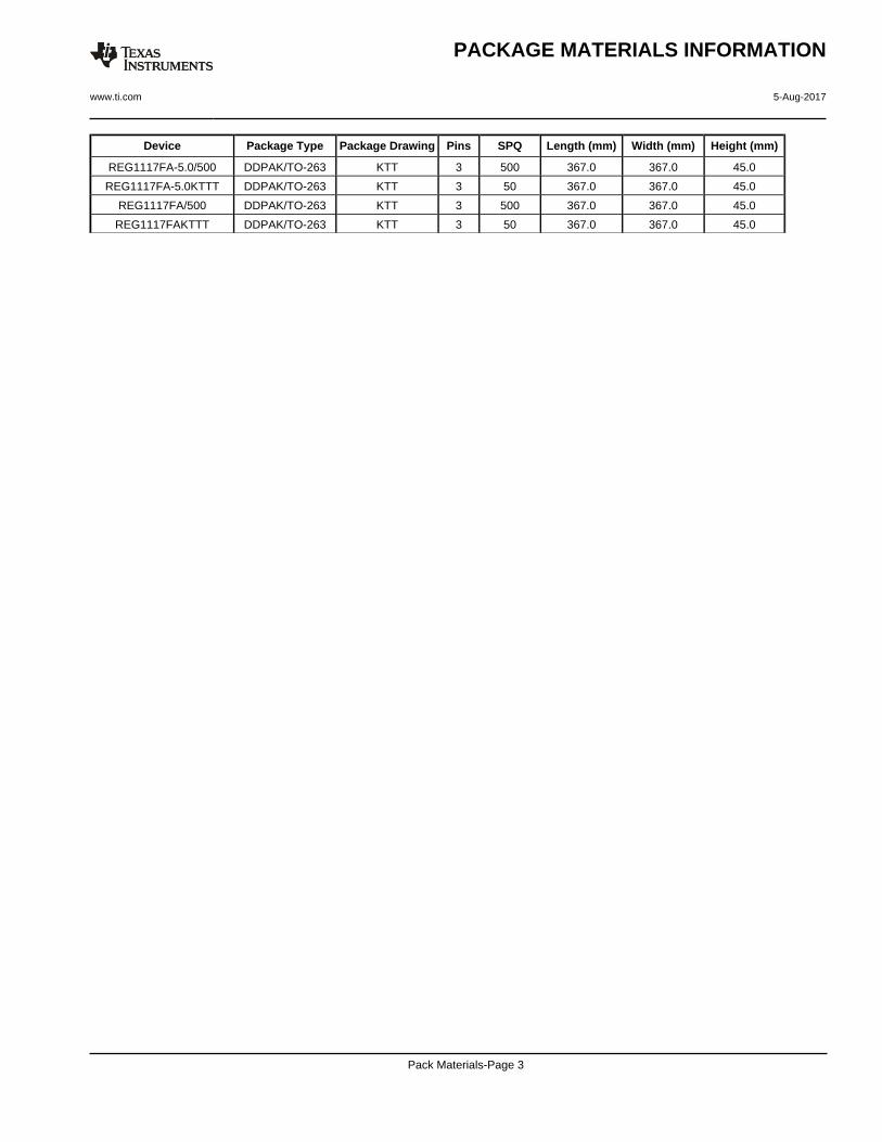
Device Package Type Package Drawing Pins SPQ Length (mm) Width (mm) Height (mm)
REG1117FA-5.0/500 DDPAK/TO-263 KTT 3 500 367.0 367.0 45.0
REG1117FA-5.0KTTT DDPAK/TO-263 KTT 3 50 367.0 367.0 45.0
REG1117FA/500 DDPAK/TO-263 KTT 3 500 367.0 367.0 45.0
REG1117FAKTTT DDPAK/TO-263 KTT 3 50 367.0 367.0 45.0
PACKAGE MATERIALS INFORMATION
www.ti.com 5-Aug-2017
Pack Materials-Page 3
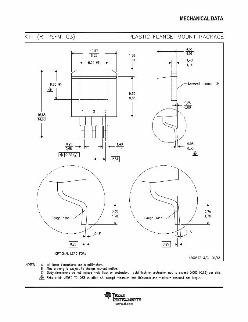


MECHANICAL DATA
MPDS094A – APRIL 2001 – REVISED JUNE 2002
POST OFFICE BOX 655303 • DALLAS, TEXAS 75265
DCY (R-PDSO-G4) PLASTIC SMALL-OUTLINE
4202506/B 06/2002
6,30 (0.248)6,70 (0.264)
2,90 (0.114)3,10 (0.122)
6,70 (0.264)7,30 (0.287) 3,70 (0.146)
3,30 (0.130)
0,02 (0.0008)0,10 (0.0040)
1,50 (0.059)1,70 (0.067)
0,23 (0.009)0,35 (0.014)
1 2 3
4
0,66 (0.026)0,84 (0.033)
1,80 (0.071) MAX
Seating Plane
0°–10°
Gauge Plane
0,75 (0.030) MIN
0,25 (0.010)
0,08 (0.003)
0,10 (0.004) M
2,30 (0.091)
4,60 (0.181) M0,10 (0.004)
NOTES: A. All linear dimensions are in millimeters (inches).B. This drawing is subject to change without notice.C. Body dimensions do not include mold flash or protrusion.D. Falls within JEDEC TO-261 Variation AA.


IMPORTANT NOTICE
Texas Instruments Incorporated (TI) reserves the right to make corrections, enhancements, improvements and other changes to itssemiconductor products and services per JESD46, latest issue, and to discontinue any product or service per JESD48, latest issue. Buyersshould obtain the latest relevant information before placing orders and should verify that such information is current and complete.TI’s published terms of sale for semiconductor products (http://www.ti.com/sc/docs/stdterms.htm) apply to the sale of packaged integratedcircuit products that TI has qualified and released to market. Additional terms may apply to the use or sale of other types of TI products andservices.Reproduction of significant portions of TI information in TI data sheets is permissible only if reproduction is without alteration and isaccompanied by all associated warranties, conditions, limitations, and notices. TI is not responsible or liable for such reproduceddocumentation. Information of third parties may be subject to additional restrictions. Resale of TI products or services with statementsdifferent from or beyond the parameters stated by TI for that product or service voids all express and any implied warranties for theassociated TI product or service and is an unfair and deceptive business practice. TI is not responsible or liable for any such statements.Buyers and others who are developing systems that incorporate TI products (collectively, “Designers”) understand and agree that Designersremain responsible for using their independent analysis, evaluation and judgment in designing their applications and that Designers havefull and exclusive responsibility to assure the safety of Designers' applications and compliance of their applications (and of all TI productsused in or for Designers’ applications) with all applicable regulations, laws and other applicable requirements. Designer represents that, withrespect to their applications, Designer has all the necessary expertise to create and implement safeguards that (1) anticipate dangerousconsequences of failures, (2) monitor failures and their consequences, and (3) lessen the likelihood of failures that might cause harm andtake appropriate actions. Designer agrees that prior to using or distributing any applications that include TI products, Designer willthoroughly test such applications and the functionality of such TI products as used in such applications.TI’s provision of technical, application or other design advice, quality characterization, reliability data or other services or information,including, but not limited to, reference designs and materials relating to evaluation modules, (collectively, “TI Resources”) are intended toassist designers who are developing applications that incorporate TI products; by downloading, accessing or using TI Resources in anyway, Designer (individually or, if Designer is acting on behalf of a company, Designer’s company) agrees to use any particular TI Resourcesolely for this purpose and subject to the terms of this Notice.TI’s provision of TI Resources does not expand or otherwise alter TI’s applicable published warranties or warranty disclaimers for TIproducts, and no additional obligations or liabilities arise from TI providing such TI Resources. TI reserves the right to make corrections,enhancements, improvements and other changes to its TI Resources. TI has not conducted any testing other than that specificallydescribed in the published documentation for a particular TI Resource.Designer is authorized to use, copy and modify any individual TI Resource only in connection with the development of applications thatinclude the TI product(s) identified in such TI Resource. NO OTHER LICENSE, EXPRESS OR IMPLIED, BY ESTOPPEL OR OTHERWISETO ANY OTHER TI INTELLECTUAL PROPERTY RIGHT, AND NO LICENSE TO ANY TECHNOLOGY OR INTELLECTUAL PROPERTYRIGHT OF TI OR ANY THIRD PARTY IS GRANTED HEREIN, including but not limited to any patent right, copyright, mask work right, orother intellectual property right relating to any combination, machine, or process in which TI products or services are used. Informationregarding or referencing third-party products or services does not constitute a license to use such products or services, or a warranty orendorsement thereof. Use of TI Resources may require a license from a third party under the patents or other intellectual property of thethird party, or a license from TI under the patents or other intellectual property of TI.TI RESOURCES ARE PROVIDED “AS IS” AND WITH ALL FAULTS. TI DISCLAIMS ALL OTHER WARRANTIES ORREPRESENTATIONS, EXPRESS OR IMPLIED, REGARDING RESOURCES OR USE THEREOF, INCLUDING BUT NOT LIMITED TOACCURACY OR COMPLETENESS, TITLE, ANY EPIDEMIC FAILURE WARRANTY AND ANY IMPLIED WARRANTIES OFMERCHANTABILITY, FITNESS FOR A PARTICULAR PURPOSE, AND NON-INFRINGEMENT OF ANY THIRD PARTY INTELLECTUALPROPERTY RIGHTS. TI SHALL NOT BE LIABLE FOR AND SHALL NOT DEFEND OR INDEMNIFY DESIGNER AGAINST ANY CLAIM,INCLUDING BUT NOT LIMITED TO ANY INFRINGEMENT CLAIM THAT RELATES TO OR IS BASED ON ANY COMBINATION OFPRODUCTS EVEN IF DESCRIBED IN TI RESOURCES OR OTHERWISE. IN NO EVENT SHALL TI BE LIABLE FOR ANY ACTUAL,DIRECT, SPECIAL, COLLATERAL, INDIRECT, PUNITIVE, INCIDENTAL, CONSEQUENTIAL OR EXEMPLARY DAMAGES INCONNECTION WITH OR ARISING OUT OF TI RESOURCES OR USE THEREOF, AND REGARDLESS OF WHETHER TI HAS BEENADVISED OF THE POSSIBILITY OF SUCH DAMAGES.Unless TI has explicitly designated an individual product as meeting the requirements of a particular industry standard (e.g., ISO/TS 16949and ISO 26262), TI is not responsible for any failure to meet such industry standard requirements.Where TI specifically promotes products as facilitating functional safety or as compliant with industry functional safety standards, suchproducts are intended to help enable customers to design and create their own applications that meet applicable functional safety standardsand requirements. Using products in an application does not by itself establish any safety features in the application. Designers mustensure compliance with safety-related requirements and standards applicable to their applications. Designer may not use any TI products inlife-critical medical equipment unless authorized officers of the parties have executed a special contract specifically governing such use.Life-critical medical equipment is medical equipment where failure of such equipment would cause serious bodily injury or death (e.g., lifesupport, pacemakers, defibrillators, heart pumps, neurostimulators, and implantables). Such equipment includes, without limitation, allmedical devices identified by the U.S. Food and Drug Administration as Class III devices and equivalent classifications outside the U.S.TI may expressly designate certain products as completing a particular qualification (e.g., Q100, Military Grade, or Enhanced Product).Designers agree that it has the necessary expertise to select the product with the appropriate qualification designation for their applicationsand that proper product selection is at Designers’ own risk. Designers are solely responsible for compliance with all legal and regulatoryrequirements in connection with such selection.Designer will fully indemnify TI and its representatives against any damages, costs, losses, and/or liabilities arising out of Designer’s non-compliance with the terms and provisions of this Notice.
Mailing Address: Texas Instruments, Post Office Box 655303, Dallas, Texas 75265Copyright © 2017, Texas Instruments Incorporated