research on design and firing performance of si-based detonator · research on design and firing...
TRANSCRIPT

Research on design and firing performance of Si-based detonator
Rui-zhen XIE*, Xiao-ming REN, Lan LIU, Yan XUE, Dong-xiao FU, Rui ZHANG
Science and Technology on Applied Physical Chemistry Laboratory, Shaanxi Applied Physics-Chemistry Research Institute, Xi’an 710061, China
Received 25 November 2013; revised 30 December 2013; accepted 6 January 2014
Available online 24 January 2014
Abstract
For the chip integration of MEMS (micro-electromechanical system) safety and arming device, a miniature detonator needs to be developedto reduce the weight and volume of explosive train. A Si-based micro-detonator is designed and fabricated, which meets the requirement ofMEMS safety and arming device. The firing sensitivity of micro-detonator is tested according to GJB/z377A-94 sensitivity test methods:Langlie. The function time of micro-detonator is measured using wire probe and photoelectric transducer. The result shows the average firingvoltage is 6.4 V when the discharge capacitance of firing electro-circuit is 33 mF. And the average function time is 5.48 ms. The firing energyactually utilized by Si-based micro-detonator is explored.Copyright � 2014, China Ordnance Society. Production and hosting by Elsevier B.V. All rights reserved.
Keywords: MEMS safety and arming device; Initiating device; Si-based detonator; Firing sensitivity; Function time
1. Introduction
With the development of ammunition technology, thedeveloping trends of fuze technology should be miniaturiza-tion, smart, high reliability and low cost [1]. Traditional safetyand arming device can accomplish the safety and armingfunctions of fuze, but it is not available for small-caliberammunition because of its large size, many parts and pooranti-overload capability [2]. MEMS safety and arming devicehas small size, light weight and good anti-overload capability,which makes conventional fuze has more space to accom-modate the multi-sensor detection circuit and the main chargeto improve the precision and lethality of ammunition [3,4]. Inrecent years, the U.S. fuze annual conferences reported thatthe performance of on-chip-based safety and arming device istested using the missile warhead at present [5e8], and the
development trend of fuze technology is on-chip integration ofmachinery, electronics and pyrotechnics in the future. Themicro-detonator has been paid more and more attention as onekey technology of MEMS fuze safety and arming device. Inthis paper, Si-based micro-detonator was designed and fabri-cated, its firing sensitivity, function time, firing energy weretested, and the test results were analyzed.
2. Design and fabrication of Si-based micro-detonator
The design idea of Si-based micro-detonator is to break-through the traditional concept of the minimum primer chargemass for achieving sub-milligram charge. Fabrication ofmicro-detonator is to use MEMS fabrication process supple-mented by other technical means to achieve the integrationmanufacture of igniter resistor and charge chamber. Thecharge chamber is made of silicon and glass, etc.
Si-based micro-detonator was designed according to thedesign idea and MEMS fabrication process. Fig. 1 shows theprinciple structure of micro-detonator, which contains chargelayer 1, igniter resistor 2(NieCr film bridge), substrate 3, andprimer charge. The charge layer 1 has a chamber which isfilled with the energetic material, and the igniter resistor 2 isfabricated on the Pyrex7740 glass substrate 3. Pyrex7740 glass
* Corresponding author.
E-mail address: [email protected] (R.Z. XIE).
Peer review under responsibility of China Ordnance Society.
Production and hosting by Elsevier
Available online at www.sciencedirect.com
ScienceDirect
Defence Technology 10 (2014) 34e39 www.elsevier.com/locate/dt
2214-9147/$ - see front matter Copyright � 2014, China Ordnance Society. Production and hosting by Elsevier B.V. All rights reserved.
http://dx.doi.org/10.1016/j.dt.2014.01.002

substrate has much lower thermal conductivity compared tothat of silicon substrate, and is easily integrated with chargelayer.
The igniter resistor is fabricated on the double-polishedPyrex7740 glass substrate [9,10]. In the first step, the sub-strate is cleaned using a special solvent, thoroughly rinsed bydeionized (DI) water, and blow-dried by nitrogen. And thenthe glass substrate is placed into a hotplate at 120 �C for10 min for further drying. In the second step, a metal layer ofNieCr is deposited on the glass substrate by sputtering. TheNieCr film acts as the bridge area of igniter resistor. In thethird step, a positive photoresist is spincoated onto thePyrex7740 glass substrate and patterned using photolithog-raphy, and then the exposed photoresist is removed by resistdeveloper. After the substrate is put into NieCr etchant(HCLO4 þ Ce2(SO4)3 þ H2O), the designed NieCr filmbridge area comes into being.
A metal layer of 1.5 mm-thick Al film is deposited onto theNieCr film layer by sputtering after NieCr film bridge area isfinished. The Al film acts as the bonding pad. A positivephotoresist is also spincoated onto Al film layer and patterned,and the exposed photoresist is then removed. After the substrateis put into Al etchant (HPO4þHNO3þCH3COOH þ H2O) at60 �C, the designed bonding pad is formed. The glass wafer withthe NieCr film heating resistor is blown-dried with nitrogenafter cleaning and then put into an oven with nitrogen flux at250 �C for 20min Fig. 2 illustrates the photograph ofNieCrfilmbridge igniter resistor.
The fabrication process of charge chamber starts with a0.5 mm-thick double-polished silicon chip. In the first step, thesubstrate is cleaned by RCA1 (NH4ON þ H2O2 þ H2O) at80 �C for 20 min. In the second step, a positive photoresist isspincoated onto a top of silicon chip and patterned usingphotolithography, and then the exposed photoresist is removed
by resist developer. After the silicon chip is put into etchant,the designed groove for embedding igniter resistor comes intobeing. In the third step, Al film is deposited on the othersurface of silicon substrate chip by sputtering. Then Al maskof chamber etching is fabricated by photolithography and wetetching. In the fourth step, the charge chamber is formed byInduction Couple Plasma (ICP) etching.
The assembly of micro-detonator is accomplished after theglass substrate and silicon chip is bonded together by chipe-chip anodic bonding method. Fig. 3 illustrates the process flowchart of micro-detonator. Fig. 4 illustrates the photograph ofSi-based micro-detonator without energetic material.
The micro-detonator is loaded with nano-porous copperazide. The copper azide contains a certain amount of cuprousazide because of the limit of energetic material preparationprocess. The size of charge chamber is 1.0 mm (D) � 0.5 mm(H ), and the average charge quantity is 0.93 mg. Fig. 5 il-lustrates the photograph of detonator loading with energeticmaterial.
Fig. 1. Schematic diagram of Si-based detonator.
Fig. 2. Photograph of NieCr film bridge igniter resistor.
Fig. 3. Process flow chart of Si-based initiator.
Fig. 4. Photograph of Si-based detonator.
Fig. 5. The photograph of Si-based detonator loading with energetic material.
35R.Z. XIE et al. / Defence Technology 10 (2014) 34e39

3. Performance characterization of Si-based micro-detonator
3.1. Firing sensitivity test of Si-based micro-detonator
Three sensitivity test methods, such as up-and-downmethod, Langlie method and D-optimization method, areprovided in GJB/Z377A-1994 “sensitivity test mathematicalstatistics methods”. The ideal parameter estimates can be gotusing Langlie method because the initial parameters have alittle effect on sensitivity testing results. But the process ofusing Langlie method to calculate the total parameter esti-mation is complex. Therefore, a portable personal digital as-sistant (PDA) developed by Shaanxi Applied Physics-Chemistry Research Institute [11] is used for test data pro-cessing. Its functions are mainly data entry, data processing,and data transfer, etc in sensitivity test of initiators andpyrotechnics.
The firing sensitivity of micro-detonator was tested ac-cording to GJB/z377A-94 sensitivity test method: Langlie.The resolution of the power supply is 0.01 V, the minimal andmaximum stimuli are selected to be 5 Vand 18 V, respectively,the data distribution is assumed to be normal distribution, anda mercury switch is used as a discharge switch. Standard de-viation of the test results is not altered. The firing circuit isillustrated in Fig. 6, and the capacitance of ignition capacitor is33 mF.
The firing sensitivity test results of micro-detonator arelisted in Table 1. The calculated 50% firing voltage is 6.40 V,and the standard deviation is 0.12 V. The 99.9% firing voltageis 6.78 V, the firing energy calculated by the following equa-tion is 0.76 mJ
Q¼ 1
2CU2
3.2. Function time test of Si-based micro-detonator
The test principle of function time is that the power supplyenergy is provided to the igniter resistor of detonator, at thesame time, an activation signal is given by the startup circuit,and the chronometer begins timing. The terminating circuitgives a stop signal to the chronometer when a detonationoutput exists at the output end of detonator. This time period isthe function time of detonator. An activation signal is alsogiven simultaneously when the micro-detonator initiation(start) circuit is switched on. The principle block diagram oftest is shown in Fig. 7.
The function time of micro-detonator was tested using wireprobe and photoelectric transducer. If the wire probe is usedfor test, two juxtaposed enameled copper wires are adhered tothe output end of micro-detonator. When a detonation outputexists at the output end of detonator, the stop circuit isswitched on to give a stop signal because of plasmas formedbetween two wire probes. The stop circuit consisting of pho-toelectric transducer gives a stop signal using photoelectricmethod.
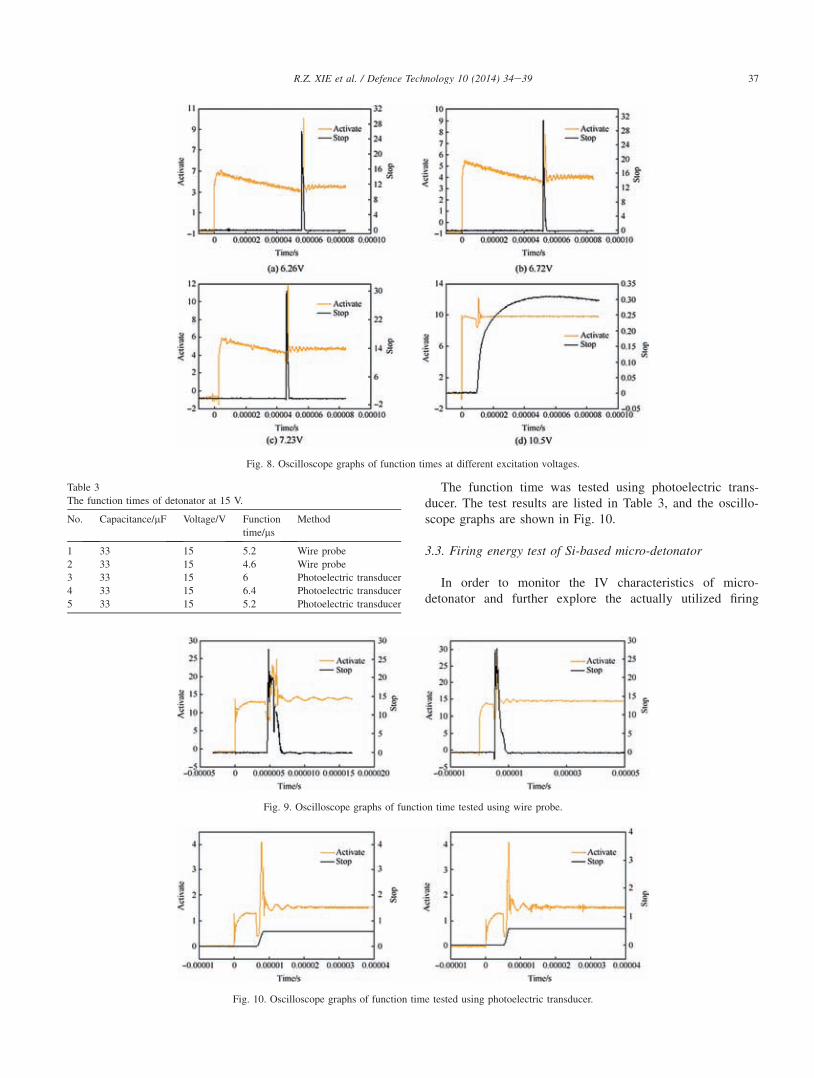
The function time at different excitation voltages was testedusing wire probe. The test results are listed in Table 2, and theoscilloscope graphs are shown in Fig. 8, (a) 6.26 V, (b) 6.72 V,(c) 7.23 V, (d) 10.5 V. The function times at 15 V excitationvoltage are listed in Table 3, and the oscilloscope graphs areshown in Fig. 9.
Fig. 6. Firing circuit of Si-based detonator.
Table 1
The test results of firing sensitivity of Si-based detonator.
No. 1 2 3 4 5 6 7 8 9 10
Voltage/V 11.5 8.25 6.62 5.81 6.22 7.23 6.72 6.26 5.63 5.94
Results 1 1 1 0 0 1 1 1 0 0
No. 11 12 13 14 15 16 17 18 19 20
Voltage/V 6.33 6.78 6.56 6.25 6.4 6.59 6.5 6.38 6.44 6.41
Results 0 1 1 0 0 1 1 0 1 0
1 Expresses firing, and 0 expresses misfire.
Fig. 7. The testing sketch of Si-based detonator’s function time.
Table 2
The function times of detonator at different excitation voltages.
No. Resistance/U Capacitance/mF Voltage/V Function time/ms
1 5.2 33 10.5 9.8
2 4.45 33 7.23 42.8
3 5.03 33 6.72 50.22
4 4.5 33 6.26 56.2
36 R.Z. XIE et al. / Defence Technology 10 (2014) 34e39
The function time was tested using photoelectric trans-ducer. The test results are listed in Table 3, and the oscillo-scope graphs are shown in Fig. 10.
3.3. Firing energy test of Si-based micro-detonator
In order to monitor the IV characteristics of micro-detonator and further explore the actually utilized firing
Fig. 8. Oscilloscope graphs of function times at different excitation voltages.
Table 3
The function times of detonator at 15 V.
No. Capacitance/mF Voltage/V Function
time/ms
Method
1 33 15 5.2 Wire probe
2 33 15 4.6 Wire probe
3 33 15 6 Photoelectric transducer
4 33 15 6.4 Photoelectric transducer
5 33 15 5.2 Photoelectric transducer
Fig. 9. Oscilloscope graphs of function time tested using wire probe.
Fig. 10. Oscilloscope graphs of function time tested using photoelectric transducer.
37R.Z. XIE et al. / Defence Technology 10 (2014) 34e39

energy, the current loop is connected with other test apparatusin series. The input current (I0) and voltage (U0) are monitoredand recorded in an oscilloscope in order to get the firing curvesfor each test of micro-detonator. The action of micro-detonatorrequires energy based on the following integral equation.
EðtÞ ¼ZT
0
Uðt0ÞIðt0Þdt0:
When the firing voltage is 15 V, the IV test results of micro-detonator are shown in Fig. 11, where (a) shows the test resultsfor 6.4 ms of function time, and (b) shows the test results for5.2 ms of function time. The integrate results of micro-detonator firing energies are shown in Fig. 12, which is
0.24 mJ and 0.20 mJ respectively. On the other hand, the firingenergies are also calculated using the following integralequation. The results of two calculating method are accordant.
EðtÞ ¼ZT
0
I2ðt0ÞRdt0
The IV characteristics of micro-detonator are tested whenthe firing voltage is 6.26 V and 6.72 V, the test results areshown in Fig. 13 where (a) shows the test results for 6.26 V,and (b) shows the test results for 6.72 V. The integrate resultsof micro-detonator firing energies are shown in Fig. 14, whichis 0.23 mJ and 0.21 mJ respectively. The result is accordantwith 15 V.
Fig. 11. The IV curve of micro-detonator (1).
Fig. 12. Firing energy of Si-based detonator (1).
Fig. 13. The IV curve of micro-detonator (2).
38 R.Z. XIE et al. / Defence Technology 10 (2014) 34e39

4. Results and discussions
Firing sensitivity of micro-detonator was tested accordingto GJB/z377A-94, the average firing voltage is 6.4 V when thecapacitor of firing circuit is 33 mF. The result shows that themicro-detonator is sensitive. Further research will be focusedon optimizing the design and reducing the firing energy tomeet the low-energy ignition requirement.
The test results show that the function time reduces linearlywith the increase in firing voltage. Both the test results ob-tained by wire probe are in agreement with those obtained byphotoelectric transducer. The average function time is 5.48 msunder 15 V, 33 mF.
The IV characteristics of micro-detonator were tested byusing current coils, and the obtained actual firing energy is0.22 mJ. The firing energy is 0.76 mJ, which is calculatedbased on 1/2CU2. The actually utilized firing energy is only29% of calculated firing energy, which is consistent with thetheoretical result in Ref. [12]. The reason is that the firingcircuit uses a part of energy, on the other hand, the initiationtime is only a small part of the RC discharge time.
5. Conclusions
A Si-based micro-detonator was designed and fabricated.Detailed design and fabrication process of each part of micro-detonator were presented, and the assembly of the two layers(Si-layer and glass layer) was described. Its operation wasvalidated by experimentation. The firing performance isexcellent for low-energy ignition and fleetly action require-ment. This paper also proposed a feasible method for testingthe actual firing energy.
In future, we plan to make further research into the inputperformance of Si-based micro-detonator to provide a reference
for its optimization design; test its output performance andoptimize its functionality design to meet the low energy ignitionand efficient output requirements of miniature munitions.
References
[1] Jiang XH, Yin Q, Tian Y, He B, Zhi YF, Zhang HB. Study on MEMS
initiators. Initiat Pyrotech 2009;6:11e3 [in Chinese].
[2] Wang SW, Hao YP, Zhang DZ, Yang F. The comprehensive analysis of
MEMS-based fuze safety and arming device. J Detect Control
2006;28(6):55e8 [in Chinese].
[3] Feng PZ, Zhu JN, Wu ZL. Analysis of US typical MEMS fuze safety &
arming device. J Detect Control 2007;29(5):26e30 [in Chinese].
[4] Pezous Helene, Rossi Carole, Sanchez Marjorie, Mathieu Fabrice,
Dollat Xavier, Charlot Samuel, et al. Fabrication, assembly and tests of a
MEMS-based safe, arm and fire device. J Phys Chem Solids
2010;71(2):75e9.[5] Lafont Renaud. Pyro-MEMS technological breakthrough in fuze domain.
In: 55th Annual NDIA fuze conference 2011.
[6] Peter JB. Next generation fuzing e maximum advantage for the war-
fighter. XM1156 precision guidance Kit(PGK) overview. In: 53th Annual
NDIA fuze conference 2009.
[7] Peter JB, Pergolizzi Anthory. XM1156 precision guidance kit (PGK)
overview. In: 54th Annual NDIA fuze conference 2010.
[8] Cope Randall. Navy overview. In: 55th Annual NDIA fuze conference
2011.
[9] Xie RZ, Ren XM, Wang KX, Xue Y, Peng ZM, Lu B. Fabrication of Ni-
Cr film igniting resistor. Chin J Energ Mater 2011;19(5):584e7 [in
Chinese].
[10] Xie RZ, Xue Y, Ren XM, Liu L, Peng ZM. Effect of bridge parameters
on the firing sensitivity of Ni-Cr alloy thin film transducer elements.
Initiat Pyrotech 2012;1:18e20 [in Chinese].
[11] Zhang R, Fu DX, Bai YW, Li F, Cheng JQ. A calculation instrument for
the sensitivity test of initiating explosive device. Initiat Pyrotech
2009;1:35e9 [in Chinese].
[12] Cai RJ. The design principle of explosive initiators. Beijing: Beijing
Institute of Technology Press; 1997 [in Chinese].
Fig. 14. Firing energy of Si-based detonator (2).
39R.Z. XIE et al. / Defence Technology 10 (2014) 34e39