*rocky j.m.lee, j.s.choi, imt co ltd, korea j.h.park ... · probe card cleaning by laser june 6 to...
TRANSCRIPT

Probe Card Cleaning by Laser
June 6 to 9, 2010
San Diego, CA USA
*Rocky J.M.Lee, J.S.Choi, IMT Co Ltd, KoreaJ.H.Park, Willtechnology Co. Ltd, Korea

June 6 to 9, 2010 IEEE SW Test Workshop 2
Contents
• PC cleaning Issues & Needs• Conventional cleaning & problems• IMT Laser cleaning technique• Advantages of laser cleaning• Results of laser cleaning• Laser cleaning systems• Summary & Conclusions• Others: LCD Probe & Socket cleaning

Key Issues & Needs Issues
: Tip Contamination in Fine pitch or MEMS probe
1. Rc increase > poor contact
2. Leakage occurrence
=> Yield drop
Needs
1. Precise cleaning tool
2. Damage free cleaning tool
=> Solution : Laser Cleaning

Background ‐ Probe Card Types
1. Cantilever PC (Epoxy)2. Vertical PC
3. MEMS PC
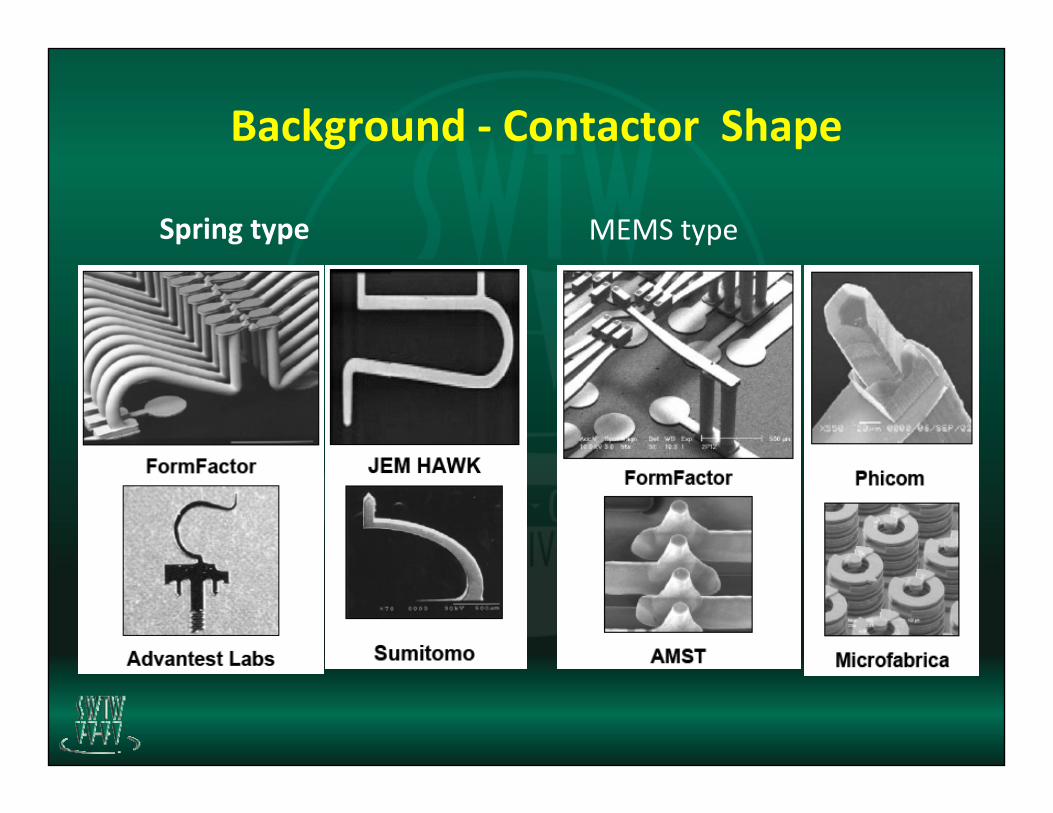
Background ‐ Contactor Shape
Spring type MEMS type
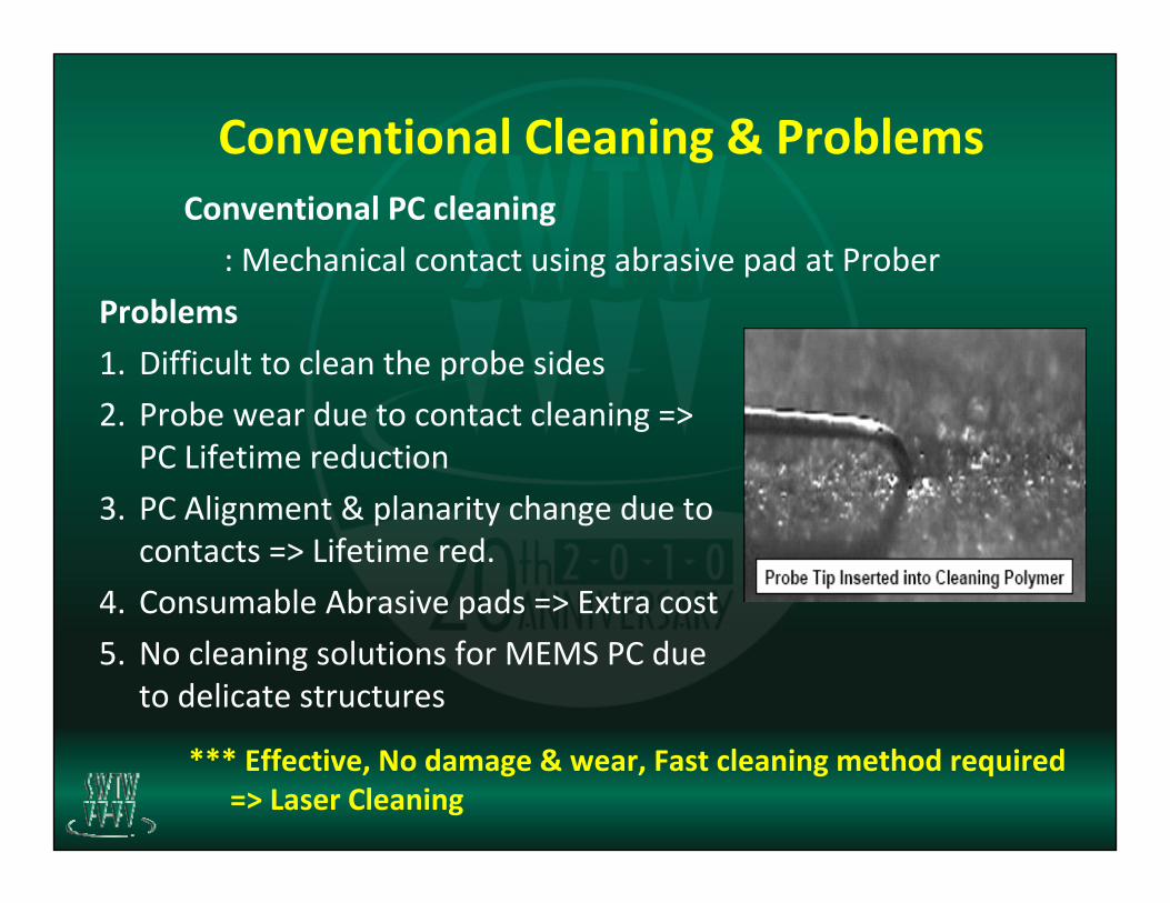
Conventional Cleaning & ProblemsConventional PC cleaning
: Mechanical contact using abrasive pad at Prober
Problems
1. Difficult to clean the probe sides
2. Probe wear due to contact cleaning => PC Lifetime reduction
3. PC Alignment & planarity change due to contacts => Lifetime red.
4. Consumable Abrasive pads => Extra cost
5. No cleaning solutions for MEMS PC due to delicate structures
*** Effective, No damage & wear, Fast cleaning method required => Laser Cleaning
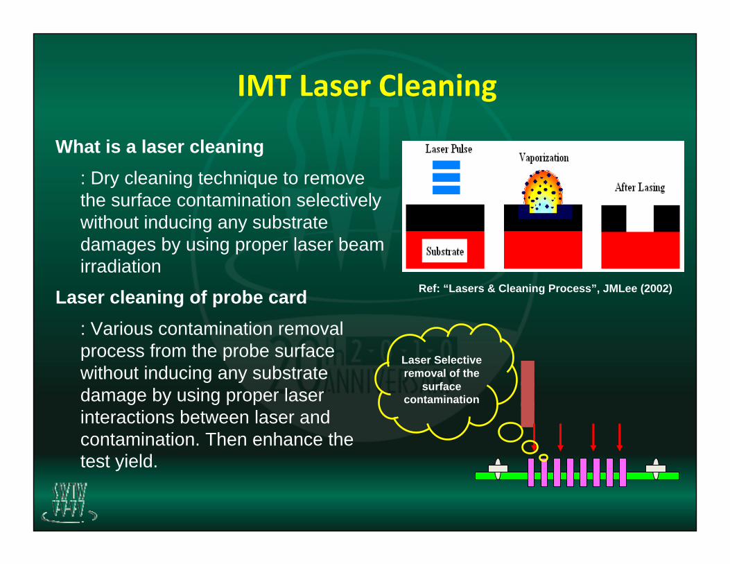
IMT Laser Cleaning
Ref: “Lasers & Cleaning Process”, JMLee (2002)
What is a laser cleaning: Dry cleaning technique to remove the surface contamination selectively without inducing any substrate damages by using proper laser beam irradiation
Laser cleaning of probe card: Various contamination removal process from the probe surface without inducing any substrate damage by using proper laser interactions between laser and contamination. Then enhance the test yield.
Laser Selective removal of the
surface contamination
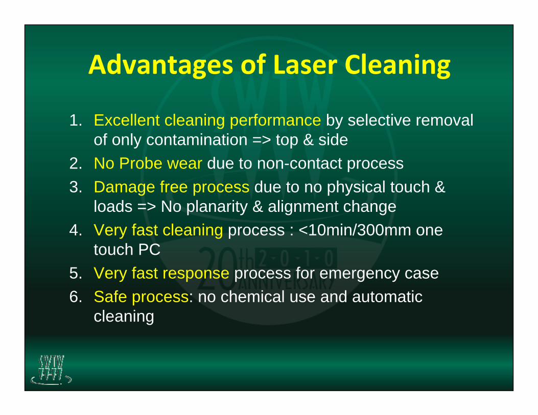
Advantages of Laser Cleaning
1. Excellent cleaning performance by selective removal of only contamination => top & side
2. No Probe wear due to non-contact process3. Damage free process due to no physical touch &
loads => No planarity & alignment change4. Very fast cleaning process : <10min/300mm one
touch PC5. Very fast response process for emergency case6. Safe process: no chemical use and automatic
cleaning

Cantilever PCs – W, ReW

Cantilever Type PC
• The Samples before Laser Cleaning
Laser Treated Area
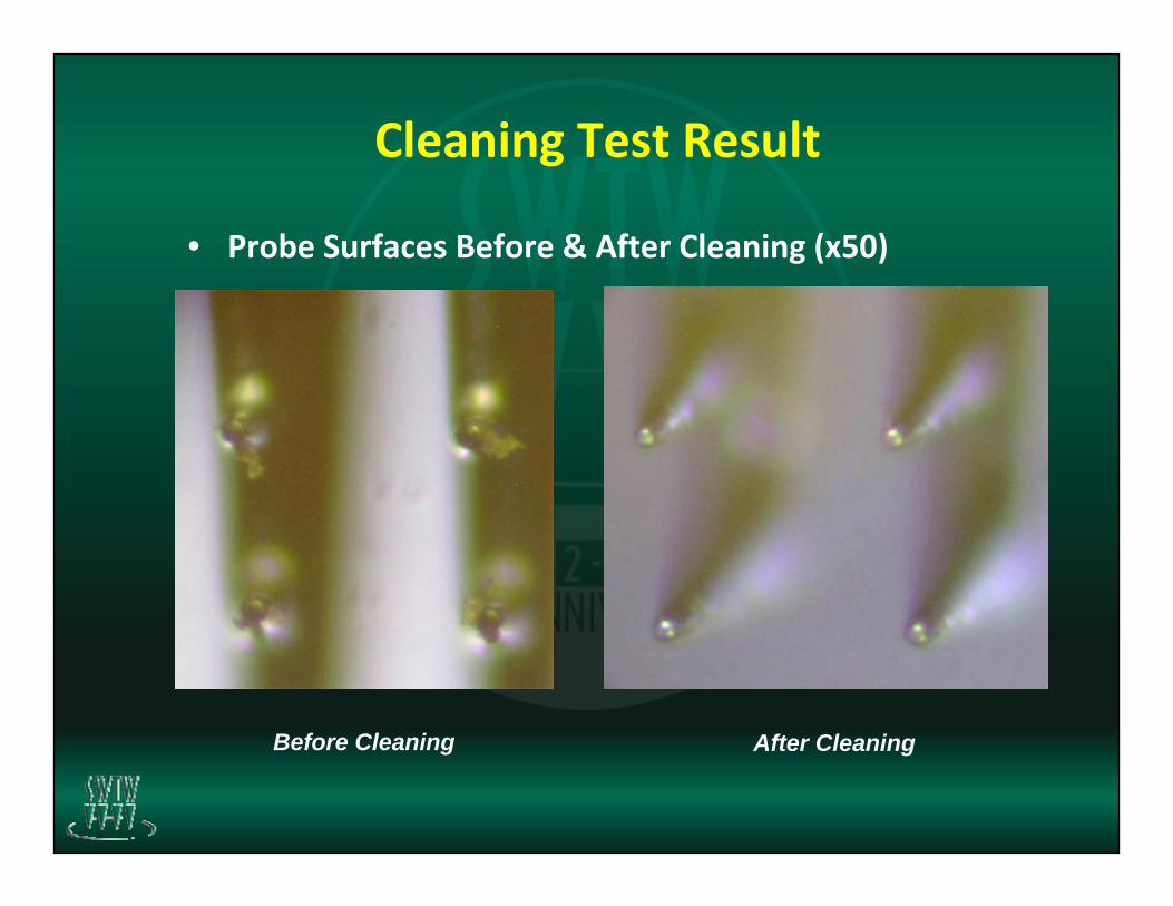
Cleaning Test Result
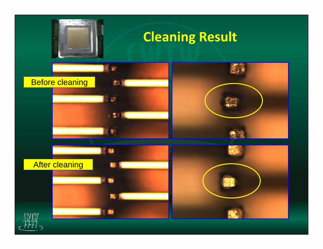
• Probe Surfaces Before & After Cleaning (x50)
Before Cleaning After Cleaning
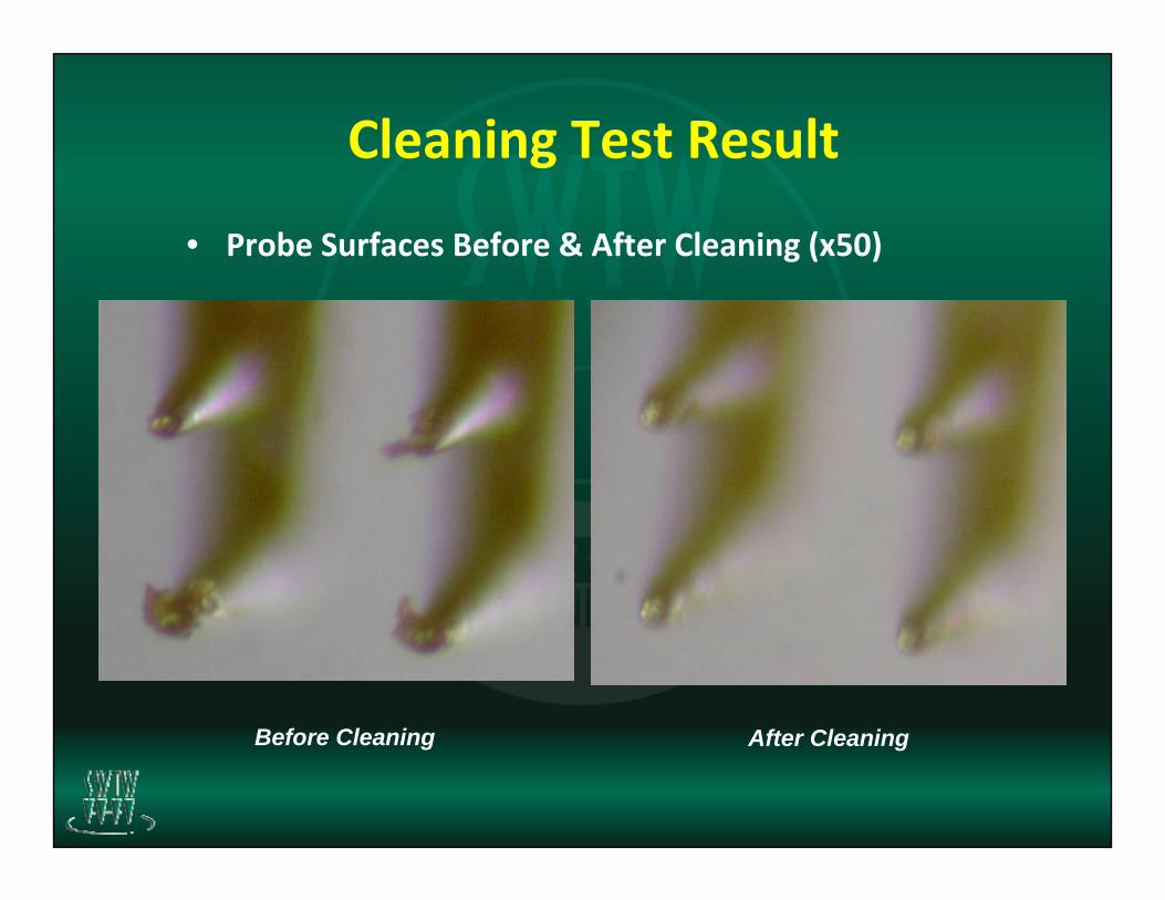
Cleaning Test Result
• Probe Surfaces Before & After Cleaning (x50)
Before Cleaning After Cleaning
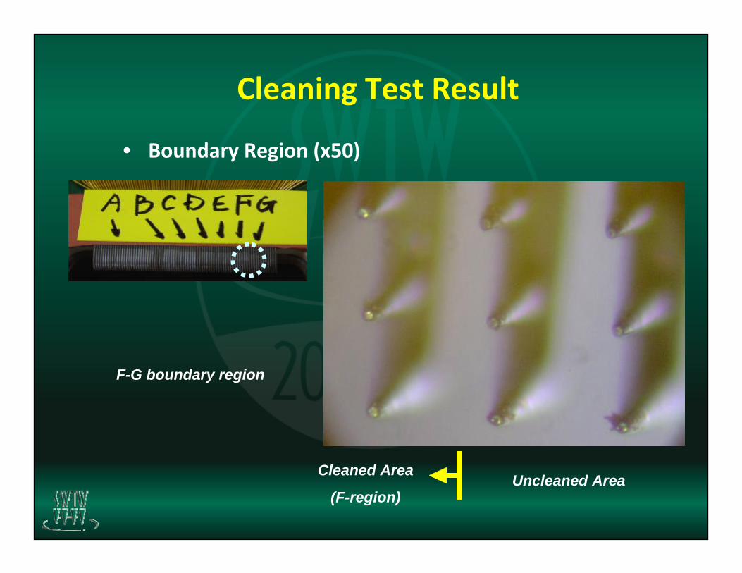
Cleaning Test Result
• Boundary Region (x50)
Cleaned Area
(F-region)Uncleaned Area
F-G boundary region

4 Layer Cantilever PC
• Probe Card for IC driver chip
Cleaning Area
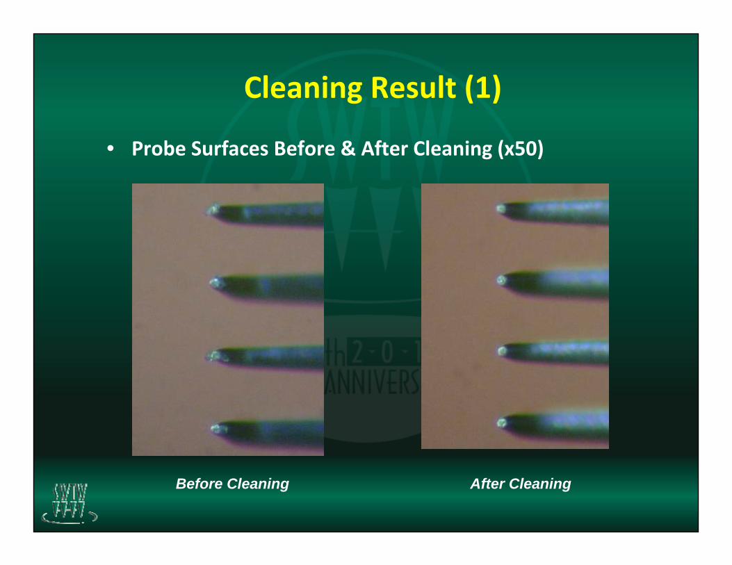
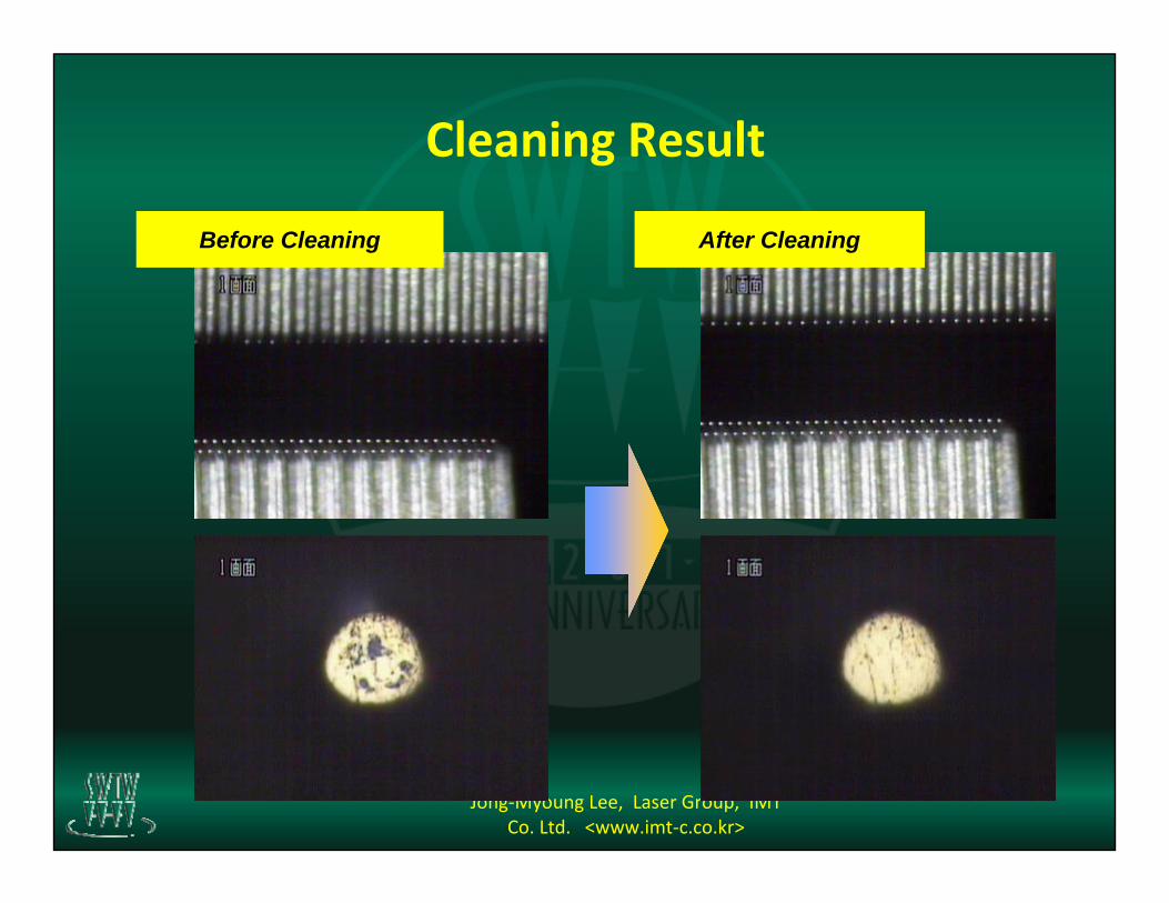
Cleaning Result (1)
• Probe Surfaces Before & After Cleaning (x50)
Before Cleaning After Cleaning
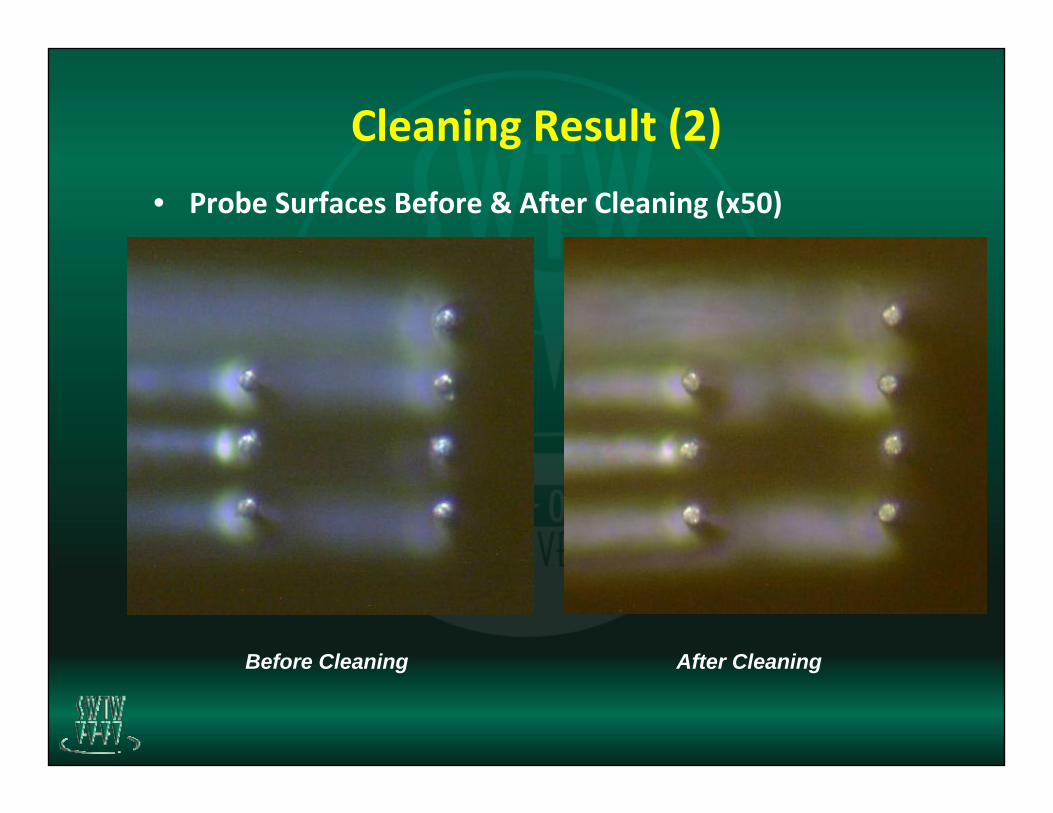
Cleaning Result (2)
• Probe Surfaces Before & After Cleaning (x50)
Before Cleaning After Cleaning

Cleaning Result ‐ details
• Magnified Tip Surface (x200)
Before cleaning
After cleaning

Cantilever PC – W‐Pt
• W‐Pt Probe Card for High speed performance
Cleaning Area
Jong‐Myoung Lee, Laser Group, IMT Co. Ltd. <www.imt‐c.co.kr>
Cleaning Result
Before Cleaning After Cleaning

Jong‐Myoung Lee, Laser Group, IMT Co. Ltd. <www.imt‐c.co.kr>
Electrical Test : Rc Measure
ItemTip surface
effectiveness
increased
Value decreased
Before Laser
Cleaning
[사진 1.]
After Laser
Cleaning
[사진 2.]
[사진 1.]과 같이 Tip의 산화 및 이물질 발생시 제품의 품질 저하 발생.
Tip의 산화 및 이물질 제거로 인해 [사진 2.]와 같이 제품의 성능 향상 효과 확인.
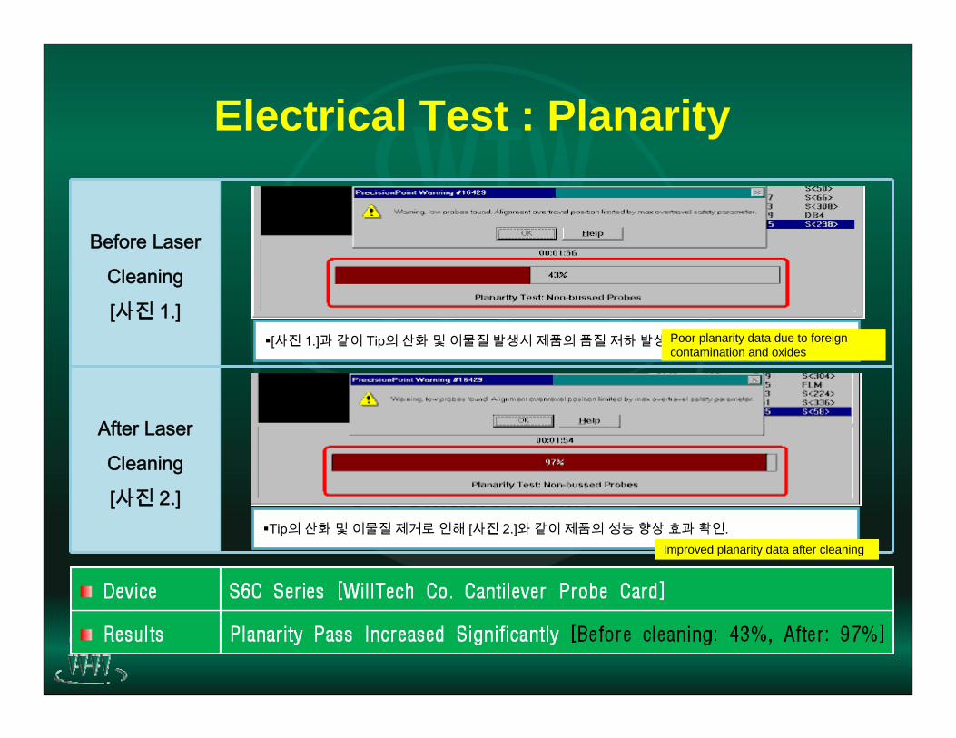
Electrical Test : Planarity
Poor planarity data due to foreign contamination and oxides
Improved planarity data after cleaning
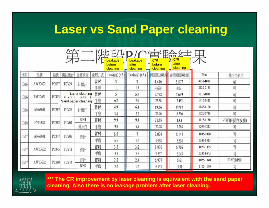
Laser vs Sand Paper cleaning
*** The CR improvement by laser cleaning is equivalent with the sand paper cleaning. Also there is no leakage problem after laser cleaning.
Laser cleaning
Sand paper cleaning
Leakage before cleaning
Leakage after cleaning
C/R before cleaning
C/R after cleaning
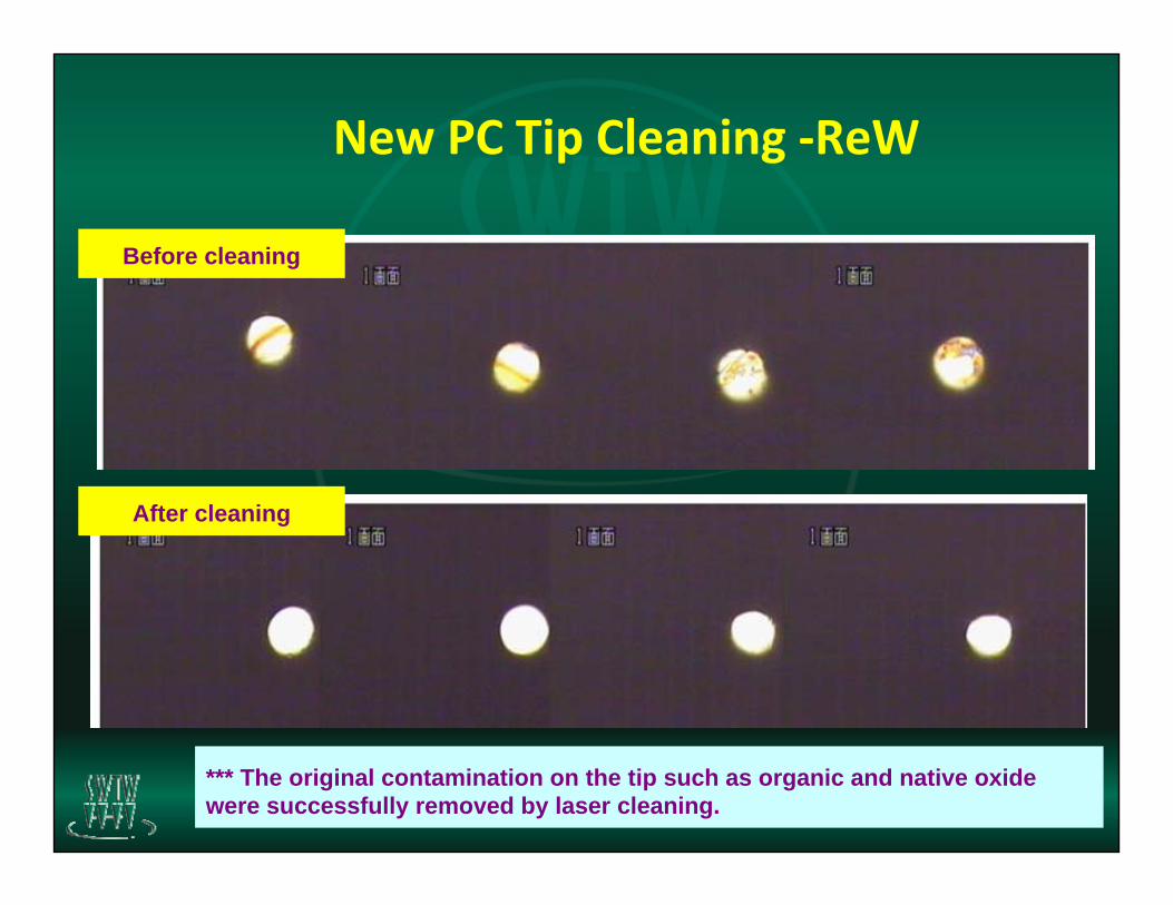
New PC Tip Cleaning ‐ReW
Before cleaning
After cleaning
*** The original contamination on the tip such as organic and native oxide were successfully removed by laser cleaning.

SEM Analysis – New PC
Before Laser Cleaning After Laser Cleaning
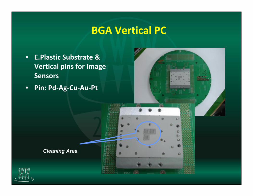
BGA Vertical PC
• E.Plastic Substrate & Vertical pins for Image Sensors
• Pin: Pd‐Ag‐Cu‐Au‐Pt
Cleaning Area
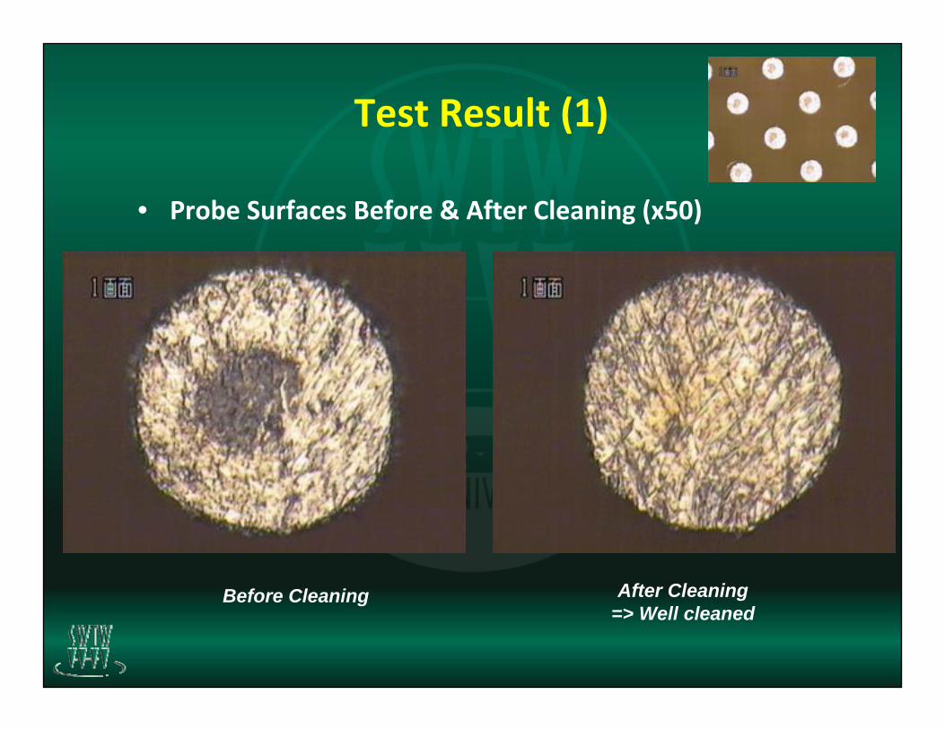
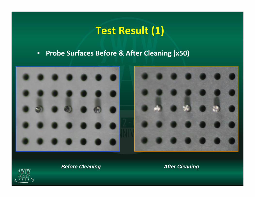
Test Result (1)
• Probe Surfaces Before & After Cleaning (x50)
Before Cleaning After Cleaning=> Well cleaned

Pogo Pin Vertical PC
• Ceramic Substrate & Pogo Pin type Probe Card
Cleaning Area
Test Result (1)
• Probe Surfaces Before & After Cleaning (x50)
Before Cleaning After Cleaning
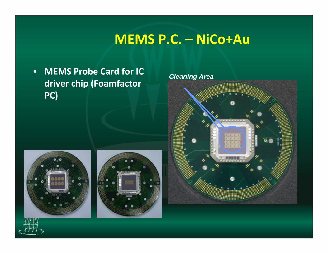
MEMS P.C. – NiCo+Au
• MEMS Probe Card for IC driver chip (Foamfactor PC)
Cleaning Area
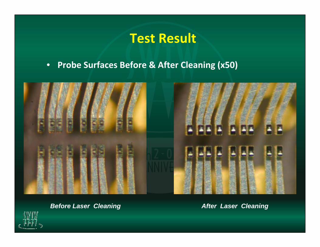
Test Result
• Probe Surfaces Before & After Cleaning (x50)
Before Laser Cleaning After Laser Cleaning

Test Result• Probe Surfaces Before & After Cleaning
Before Cleaning After Cleaning

MEMS P.C. ‐ NiCo
• MEMS Probe Card for LCD Driver IC (LDI)
Cleaning Area
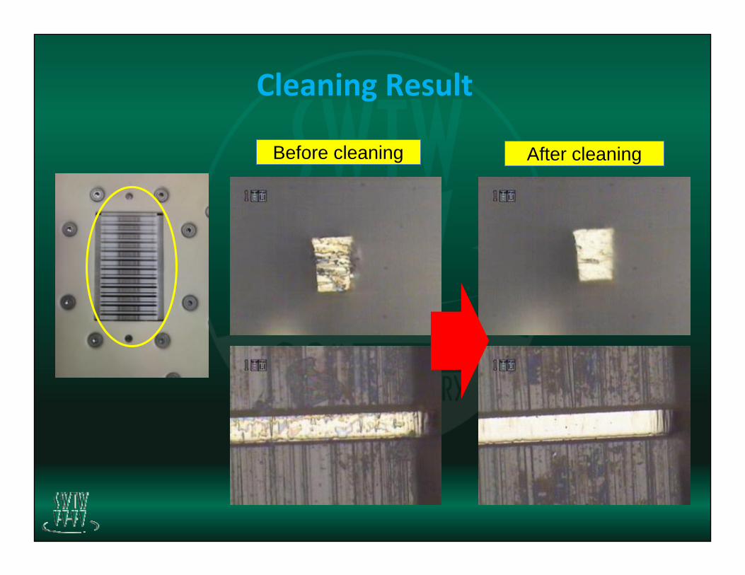
Cleaning Result
Before cleaning After cleaning
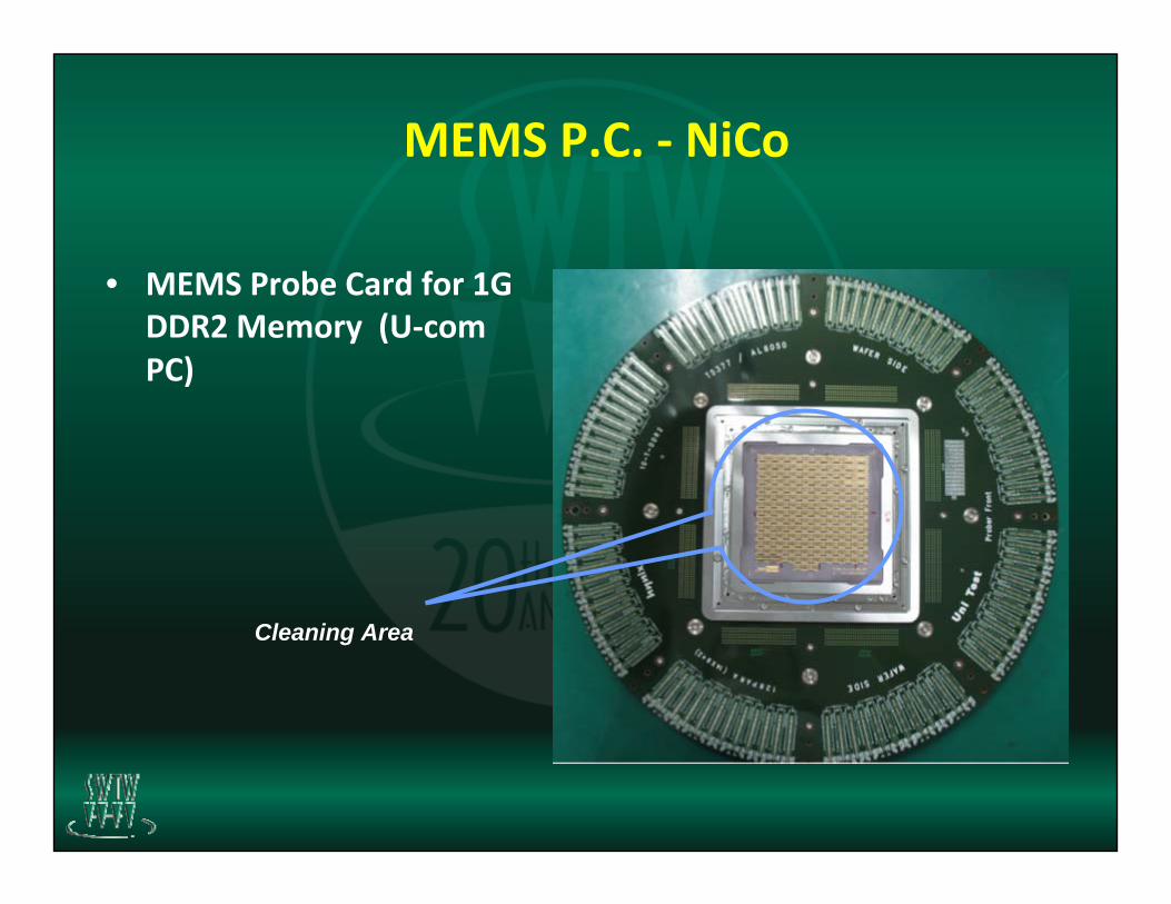
MEMS P.C. ‐ NiCo
• MEMS Probe Card for 1G DDR2 Memory (U‐com PC)
Cleaning Area
Cleaning Result
Before cleaning
After cleaning

Alignment: “Not Found” 75 channels reduced and “Passed”increased by 70 channels
Planarity: “Not Found” 740 channels reduced and “Passed”increased by 790 channels.
Functional Results after cleaning
Before cleaning
After cleaning
>> Very effective of Laser cleaning for MEMS probe card
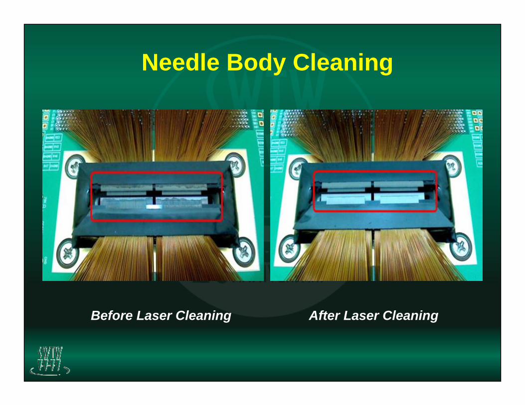
Needle Body Cleaning
Before Laser Cleaning After Laser Cleaning

Cobra Needle Cleaning (Pt)
Before cleaning
After cleaning

*** There was no any dimensional change after 1000 times of laser cleaning => No physical damage by laser
Damage Test - Dimension
210.3090μm 210.0858μm
Before Laser Cleaning After Laser Cleaning
Probe dimension before & after 1000 laser shots at 350mJ

*** There was no any surface changes after the harsh 100 laser treatment => No physical damages by laser cleaning
Damage Test - Substrate
Before treatment After treatment
Substrate & Parts before & after 100 laser shots at 350mJ
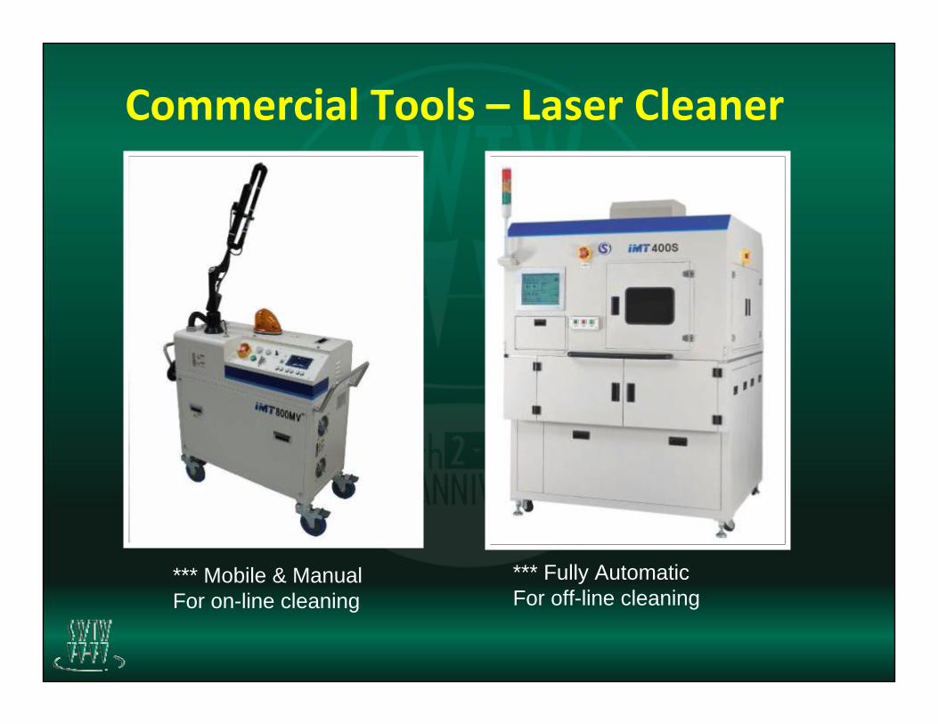
Commercial Tools – Laser Cleaner
*** Mobile & ManualFor on-line cleaning
*** Fully AutomaticFor off-line cleaning

Real Application – X‐Y Cleaning Stage
* Off-line Cleaning Stage- Manual operation
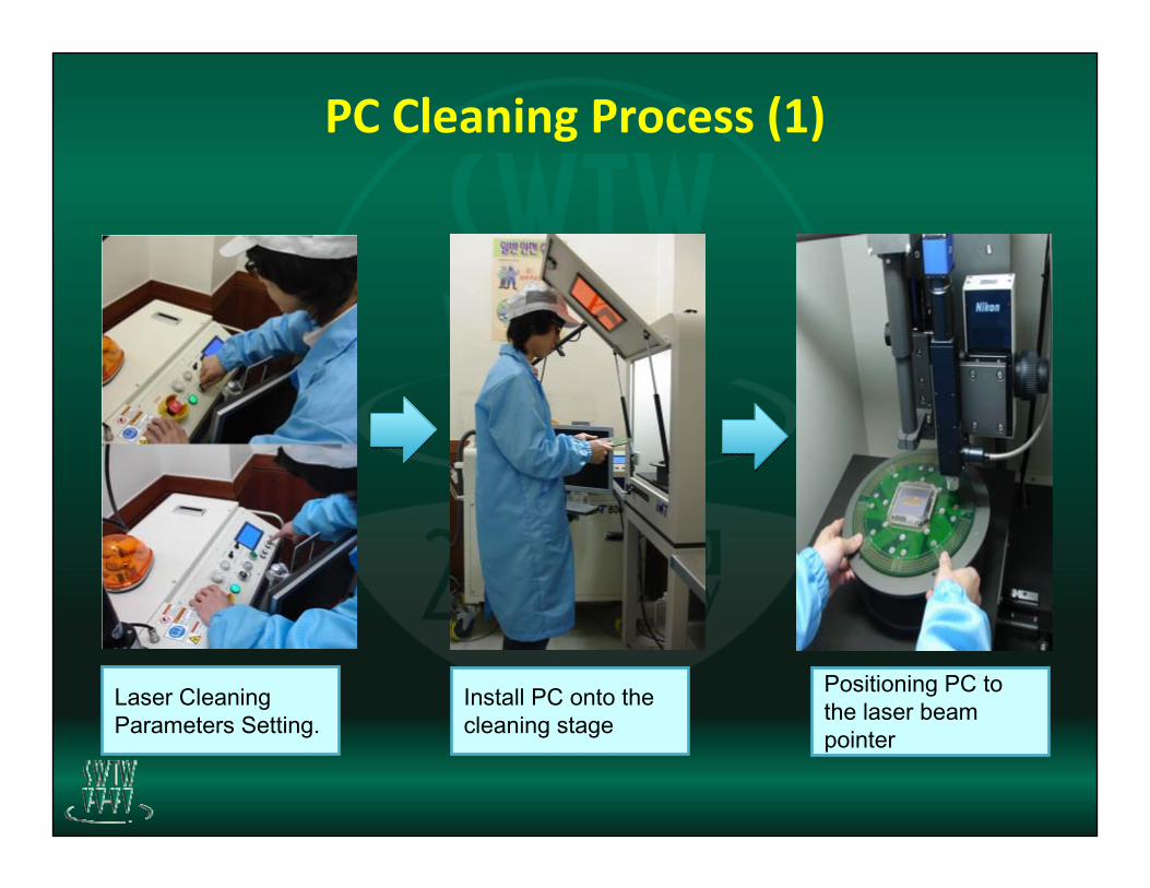
Laser Cleaning Parameters Setting.
Install PC onto the cleaning stage
Positioning PC to the laser beam pointer
PC Cleaning Process (1)
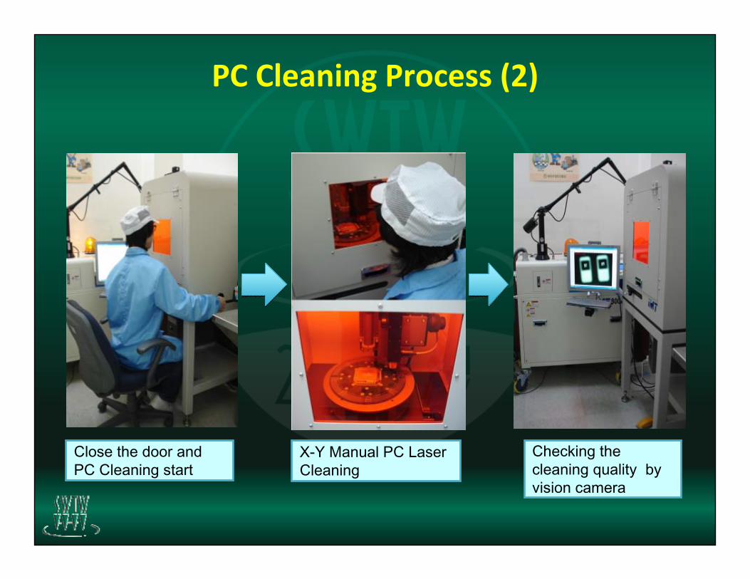
Close the door and PC Cleaning start
X-Y Manual PC Laser Cleaning
Checking the cleaning quality by vision camera
PC Cleaning Process (2)

Summary & ConclusionsLaser cleaning can be applied successfully for : 1. Canti: W, Re‐W, W‐Pt …2. Vertical: Au in BeCu(pogo), Pd‐Ag, Pd‐Co …3. MEMS: Au in Ni‐Co, Ni‐Co …
=> Without any pin & substrate damages
Laser cleaning can provides : 1. High speed cleaning even for 300mm PC2. Safe cleaning even for MEMS PC3. Quality assurance even for New PC
=> Novel Probe Card cleaning solution
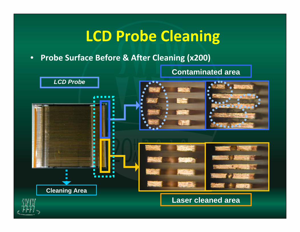
• Probe Surface Before & After Cleaning (x200)
Contaminated area
Laser cleaned areaCleaning Area
LCD Probe
LCD Probe Cleaning

3/2010 Socket Cleaning with Laser 47
Before cleaning After cleaning
Target of Test Socket Cleaning: To remove Tin(Sn) based contamination from pogo-pin surface
Test Socket Cleaning
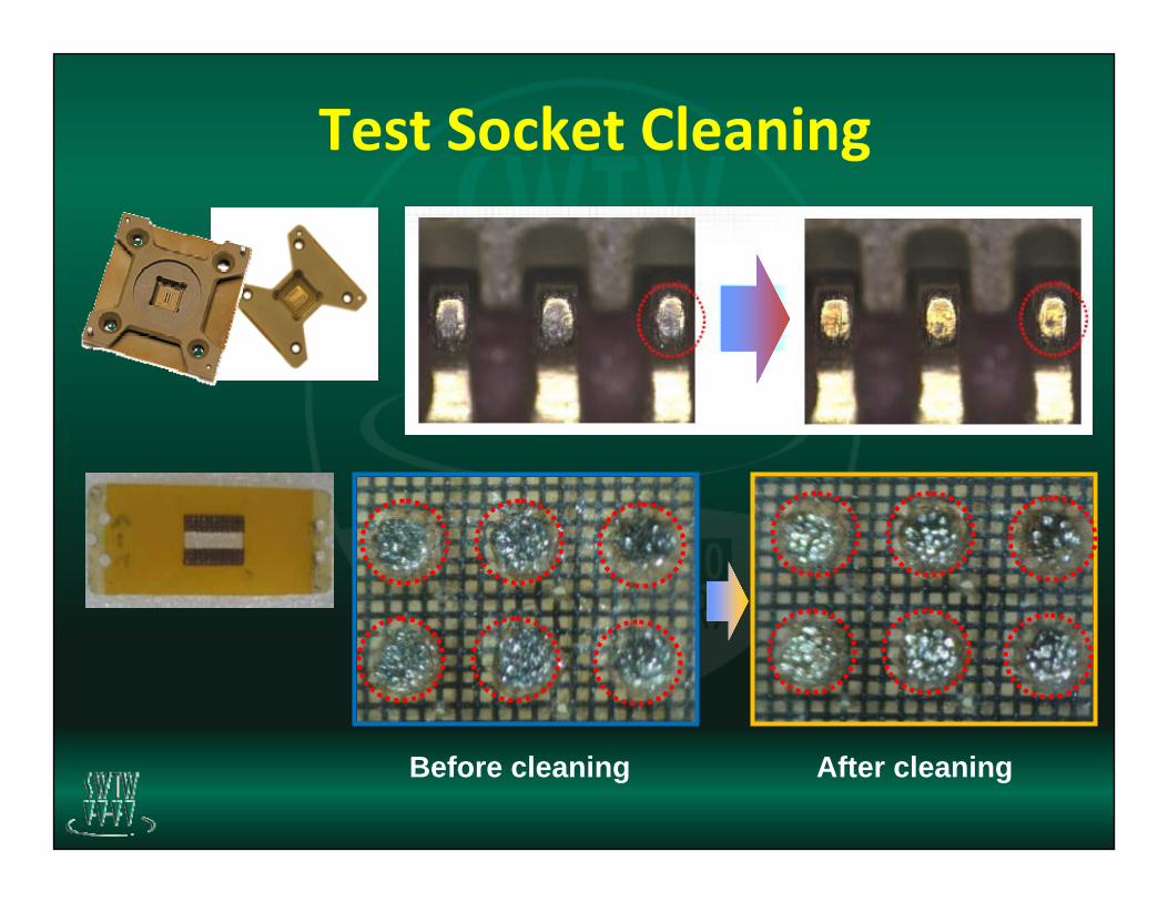
Before cleaning After cleaning
Test Socket Cleaning