slts228c december 2004 revised august … typ max unit vo =12 v 0.1 6 (1) io output current ta = 25...
TRANSCRIPT

1
6
2
3
7
VI
Inhibit
GND GND
VO
1%, 0.05 W(Required)
PTN78020
(Top View)
STANDARD APPLICATION
RSET#
4 5VO Sense
L
O
A
D
*See the section for capacitor recommendations. The minimum input capacitance
for is PTN78020W, and PTN78020H
Application Information
2.2 F for 18.8 F (4 x 4.7 F) form m m
#R oltage. See the section for values.SET Application Informationis required to adjust the output v
C *
Ceramic(Required)
IC *
330 F(Required)
O
m
PTN78020WPTN78020H
www.ti.com SLTS228C –DECEMBER 2004–REVISED AUGUST 2011
6-A, WIDE-INPUT ADJUSTABLE SWITCHING REGULATORCheck for Samples: PTN78020W, PTN78020H
1FEATURES APPLICATIONS• 6-A Output Current • General-Purpose, Industrial Controls,
HVAC Systems, Test and Measurement,• Wide-Input VoltageMedical Instrumentation, AC/DC Adaptors,(7 V to 36 V) / (15 V to 36 V)Vehicles, Marine, and Avionics• Wide-Output Voltage Adjust
(2.5 V to 12.6 V) / (11.85 V to 22 V)• High Efficiency (Up to 96%)• On/Off Inhibit• Undervoltage Lockout• Output Current Limit• Overtemperature Shutdown• Operating Temperature: -40°C to 85°C• Surface Mount Package Available
DESCRIPTIONThe PTN78020 is a series of high-efficiency, step-down integrated switching regulators (ISRs), that represent thethird generation in the evolution of high-performance power modules designed for industrial use. The wide-inputvoltage range makes these modules suitable for a variety of applications that operate off 12–V, 24–V, and 28–Vdc power. In new designs they should be considered in place of the PT6620, PT6650, PT6680, and PT6880series of single in-line pin (SIP) products. The PTN78020 is smaller and lighter than its predecessors, and haseither similar or improved electrical performance characteristics. The caseless, double-sided package hasexcellent thermal characteristics, and is compatible with TI's roadmap for RoHS and lead-free compliance.
Operating from a wide-input voltage range, the PTN78020 provides high-efficiency, step-down voltageconversion for loads of up to 6 A. The output voltage is set using a single, external resistor. The PTN78020Wmay be set to any value within the range, 2.5 V to 12.6 V, and the PTN78020H from 11.85 V to 22 V. The outputvoltage of the PTN78020W can be as little as 2 V lower than the input, allowing operation down to 7 V, with anoutput voltage of 5 V. The output voltage of the PTN78020H can be as little as 3 V lower than the input, allowingoperation down to 15 V, with an output voltage of 12 V.
The PTN78020 has undervoltage lockout, an integral on/off inhibit, and includes an output current limit andovertemperature protection.
1
Please be aware that an important notice concerning availability, standard warranty, and use in critical applications of TexasInstruments semiconductor products and disclaimers thereto appears at the end of this data sheet.
PRODUCTION DATA information is current as of publication date. Copyright © 2004–2011, Texas Instruments IncorporatedProducts conform to specifications per the terms of the TexasInstruments standard warranty. Production processing does notnecessarily include testing of all parameters.

PTN78020WPTN78020HSLTS228C –DECEMBER 2004–REVISED AUGUST 2011 www.ti.com
This integrated circuit can be damaged by ESD. Texas Instruments recommends that all integrated circuits be handled withappropriate precautions. Failure to observe proper handling and installation procedures can cause damage.
ESD damage can range from subtle performance degradation to complete device failure. Precision integrated circuits may be moresusceptible to damage because very small parametric changes could cause the device not to meet its published specifications.
ORDERING INFORMATIONFor the most current package and ordering information, see the Package Option Addendum at the end of this datasheet, or seethe TI website at www.ti.com.
ABSOLUTE MAXIMUM RATINGS (1)
over operating free-air temperature range unless otherwise notedall voltages with respect to GND
UNIT
TA Operating free-air temperature Over VI range –40°C to 85°C
Surface temperature of module body or pins Horizontal THWave solder temperature 260°C(5 seconds) (suffix AH & AD)
Horizontal SMD 235°C(suffix AS)Solder reflow temperature Surface temperature of module body or pins
Horizontal SMD 260°C(suffix AZ)
TS Storage temperature –55°C to 125°C
VI Input surge voltage, 10 ms maximum 38 V
VINH Inhibit (pin 3) input voltage –0.3 V to 5 V
PO Output power VI ≤ 24 V or VO ≥ 15 V 90 W
(1) Stresses beyond those listed under absolute maximum ratings may cause permanent damage to the device. These are stress ratingsonly, and functional operation of the device at these or any other conditions beyond those indicated under recommended operatingconditions is not implied. Exposure to absolute-maximum-rated conditions for extended periods may affect device reliability.
RECOMMENDED OPERATING CONDITIONSMIN MAX UNIT
PTN78020W 7 36VI Input voltage V
PTN78020H 15 36
TA Operating free-air temperature –40 85 °C
PACKAGE SPECIFICATIONSPTN78020x (Suffix AH, AS, & AZ)
Weight 7.3 grams
Flammability Meets UL 94 V-O
Horizontal T/H (suffix AH and AD) 250 G (1)Mechanical Per Mil-STD-883D, Method 2002.3, 1 ms, 1/2 sine,shock mounted Horizontal SMD (suffix AS and AZ) 125 G (1)
Horizontal T/H (suffix AH and AD) 20 G (1)Mechanical Mil-STD-883D, Method 2007.2, 20-2000 Hzvibration Horizontal SMD (suffix AS and AZ) 10 G (1)
(1) Qualification limit.
2 Submit Documentation Feedback Copyright © 2004–2011, Texas Instruments Incorporated
Product Folder Link(s): PTN78020W PTN78020H

PTN78020WPTN78020H
www.ti.com SLTS228C –DECEMBER 2004–REVISED AUGUST 2011
ELECTRICAL CHARACTERISTICSoperating at 25°C free-air temperature, VI = 20 V, VO = 5 V, IO = IO (max), CI = 2.2 µF, CO = 330 µF (unless otherwise noted)
PTN78020WPARAMETER TEST CONDITIONS
MIN TYP MAX UNIT
VI ≤24 V 0.1 6 (1)
IO Output current TA = 25°C, natural convection airflow VI = 32 V 0.1 5 (1) A
VI = 36 V 0.1 4.5 (1)
VI Input voltage range Over IO range 7 (2) 36 (3) V
Set-point voltage tolerance TA = 25°C ±2% (4)
Temperature variation –40°C to +85°C ±0.5%
Line regulation Over VI range ±10 mVVO
Load regulation Over IO range ±10 mV
Includes set point, line, loadTotal output voltage variation ±3% (4)
–40 < TA < 85°C
VI < 12 V 2.5 VI – 2
12 V ≤ VI ≤ 15.1 V 2.5 VI – 2.5VO (adj) Output voltage adjust range V
15.1 V < VI ≤ 25 V 2.5 12.6
VI > 25 V 0.1 × VI 12.6
VI = 24 V, RSET = 732 Ω, VO = 12 V 94%
η Efficiency VI = 15 V, RSET = 21 kΩ, VO = 5 V 88%
VI = 15 V, RSET = 78.7 kΩ, VO = 3.3 V 85%
Output voltage ripple 20-MHz bandwith 1% VO V(PP)
IO (LIM) Current limit threshold ΔVO = –50 mV 8.5 A
1 A/µs load step from 50% to 100% IOmax
Transient response Recovery time 200 µs
VO over/undershoot 5 %VO
Input high voltage (VIH) 1 Open (5)
VInhibit control (pin 3) Input low voltage (VIL) –0.1 0.3
Input low current (IIL) 0.25 mA
II(stby) Input standby current Pin 3 connected to GND 17 mA
VI increasing 5.5UVLO Undervoltage lockout V
VI decreasing 5.2
FS Switching frequency Over VI and IO ranges 440 550 660 kHz
CI External input capacitance Ceramic and nonceramic 2.2 (6) µF
Ceramic 300µF
CO External output capacitance Nonceramic 330 (7) 2,000
Equiv. series resistance (nonceramic) 10 (8) mΩ
Per Telcordia SR-332, 50% stress,MTBF Calculated reliability 5.6 106 HrTA = 40°C, ground benign
(1) Above an input voltage of 24 V, the maximum output current must be derated by 125 mA per volt above 24 V.(2) For output voltages less than 10 V, the minimum input voltage is 7 V or (VO + 2) V, whichever is greater. For output voltages of 10 V
and higher, the minimum input voltage is (VO + 2.5 V). See the Application Information section for further guidance.(3) For output voltages less than 3.6 V, the maximum input voltage is 10 × VO . See the Application Information section for further guidance.(4) The set-point voltage tolerance is affected by the tolerance and stability of RSET. The stated limit is unconditionally met if RSET has a
tolerance of 1% with with 100 ppm/°C or better temperature stability.(5) This control pin has an internal pullup, and if left open-circuit, the module operates when input power is applied. The open-circuit voltage
is typically 1.5 V. A small, low-leakage (< 100 nA) MOSFET is recommended for control. See the Application Information section forfurther guidance.
(6) An external 2.2-µF ceramic capacitor is required across the input (VI and GND) for proper operation. Locate the capacitor close to themodule.
(7) 330 µF of output capacitance is required for proper operation. See the Application Information section for further guidance.(8) This is the typical ESR for all the electrolytic (nonceramic) capacitance. Use 17 mΩ as the minimum when using max-ESR values to
calculate.
Copyright © 2004–2011, Texas Instruments Incorporated Submit Documentation Feedback 3
Product Folder Link(s): PTN78020W PTN78020H

PTN78020WPTN78020HSLTS228C –DECEMBER 2004–REVISED AUGUST 2011 www.ti.com
ELECTRICAL CHARACTERISTICSoperating at 25°C free-air temperature, VI = 24 V, VO = 12 V, IO = IO (max), CI = 4× 4.7 µF, CO = 330 µF (unless otherwisenoted)
PTN78020HPARAMETER TEST CONDITIONS
MIN TYP MAX UNIT
Vo =12 V 0.1 6 (1)
IO Output current TA = 25°C, natural convection airflow Vo =15 V 0.1 6 (1) (2) A
Vo = 22 V 0.1 4.09 (2)
VI Input voltage range Over IO range 15 (3) 36 V
Set-point voltage tolerance TA = 25°C ±2% (4)
Temperature variation –40°C to +85°C ±0.5%
Line regulation Over VI range ±10 mVVO
Load regulation Over IO range ±10 mV
Includes set point, line, loadTotal output voltage variation ±3% (4)
–40 < TA < 85°C
VI < 19 V 11.85 VI – 3
19 V ≤ VI ≤ 25 V 11.85 VI – 4VO (adj) Output voltage adjust range V
VI > 25 V 11.85 22
VI = 24 V, RSET = 383 k Ω, VO = 12 V 94%
η Efficiency VI = 24 V, RSET = 15 kΩ, VO = 15 V 95%
VI = 32 V, RSET = 95.3 Ω, VO = 22 V 96%
Output voltage ripple 20-MHz bandwith 1% VO V(PP)
IO (LIM) Current limit threshold ΔVO = –50 mV 8.0 A
1 A/µs load step from 50% to 100% IOmax
Transient response Recovery time 200 µs
VO over/undershoot 200 mV
Input high voltage (VIH) 1 Open (5)
VInhibit control (pin 3) Input low voltage (VIL) –0.1 0.3
Input low current (IIL) 0.25 mA
II(stby) Input standby current Pin 3 connected to GND 17 mA
VI increasing 12.2UVLO Undervoltage lockout V
VI decreasing 12
FS Switching frequency Over VI and IO ranges 440 550 660 kHz
CI External input capacitance Ceramic and nonceramic 18.8 (6) µF
Ceramic 0 300µF
CO External output capacitance Nonceramic 330 (7) 2,000
Equiv. series resistance (nonceramic) 10 (8) mΩ
Per Telcordia SR-332, 50% stress,MTBF Calculated reliability 5.6 106 HrTA = 40°C, ground benign
(1) The maximum output current is 6 A or a maximum output power of 90 W, whichever is less. Above an input voltage of 24 V, themaximum output current must be derated by 125 mA per volt above 24 V. See the Typica lCharacteristics section for further guidance.
(2) Above an output voltage of 15 V, the maximum output current must be derated by 285 mA per volt. The maximum output power is 90 W.See the application information for further guidance.
(3) For output voltages less than 19 V, the minimum input voltage is 15 V or (VO + 3) V, whichever is greater. For output voltages of 19 Vand higher, the minimum input voltage is (VO + 4 V). See the Application Information section for further guidance.
(4) The set-point voltage tolerance is affected by the tolerance and stability of RSET. The stated limit is unconditionally met if RSET has atolerance of 1% with with 100 ppm/°C or better temperature stability.
(5) This control pin has an internal pullup, and if left open-circuit, the module operates when input power is applied. The open-circuit voltageis typically 1.5 V. A small, low-leakage (< 100 nA) MOSFET is recommended for control. See the Application Information section forfurther guidance.
(6) Four external 4.7-µF ceramic capacitors are required across the input (VI and GND) for proper operation. Locate the capacitors close tothe module.
(7) 330 µF of output capacitance is required for proper operation. See the Application Information section for further guidance.(8) This is the typical ESR for all the electrolytic (nonceramic) capacitance. Use 17 mΩ as the minimum when using max-ESR values to
calculate.
4 Submit Documentation Feedback Copyright © 2004–2011, Texas Instruments Incorporated
Product Folder Link(s): PTN78020W PTN78020H

PTN78020(Top View)
1
2
7
6
543
PTN78020WPTN78020H
www.ti.com SLTS228C –DECEMBER 2004–REVISED AUGUST 2011
PIN ASSIGNMENT
TERMINAL FUNCTIONSTERMINAL
I/O DESCRIPTIONNAME NO.
This is the common ground connection for the VI and VO power connections. It is also the 0-Vdc referenceGND 1, 7 for the Inhibit and VO Adjust control inputs.
VI 2 I The positive input voltage power node to the module, which is referenced to common GND.
The Inhibit pin is an open-collector/drain active-low input that is referenced to GND. Applying a low-levelground signal to this input disables the module's output and turns off the output voltage. When the InhibitInhibit 3 I control is active, the input current drawn by the regulator is significantly reduced. If the Inhibit pin is leftopen-circuit, the module produces an output whenever a valid input source is applied.
A 1% resistor must be connected between this pin and GND (pin 7) to set the output voltage of themodule. If left open-circuit, the output voltage is set to its default value. The temperature stability of theVO Adjust 4 I resistor should be 100 ppm/°C (or better). The standard resistor value for a number of common outputvoltages is provided in the application information.
The sense input allows the regulation circuit to compensate for voltage drop between the module and theVO Sense 5 I load. For optimum voltage accuracy, VO Sense should be connected to VO . If the
sense feature is not used, this pin may be left disconnected.
VO 6 O The regulated positive power output with respect to the GND node.
Copyright © 2004–2011, Texas Instruments Incorporated Submit Documentation Feedback 5
Product Folder Link(s): PTN78020W PTN78020H

0
10
20
30
40
50
0 1 2 3 4 5 6
IO - Output Current - A
V-
Ou
tpu
t V
olt
ag
e R
ipp
le -
mV
OP
P
VO = 3.3 VVO = 5 V
0
1
2
3
4
0 1 2 3 4 5 6
P-
Po
we
r D
iss
ipa
tio
n -
WD
IO - Output Current - A
VO = 3.3 V
VO = 5 V
0 1 2 3 4 5 650
60
70
80
90
100
VO = 3.3 V
VO = 5 V
Eff
icie
nc
y -
%
IO - Output Current - A
20
30
40
50
60
70
80
90
0 1 2 3 4 5 6
IO - Output Current - A
200 LFM
100 LFM
Nat conv
Te
mp
era
ture
De
rati
ng
-C
o Airflow
VO = 3.3 V
20
30
40
50
60
70
80
90
0 1 2 3 4 5 6
IO - Output Current - A
200 LFM
100 LFM
Nat conv
Te
mp
era
ture
De
rati
ng
-C
o Airflow
VO = 5 V
PTN78020WPTN78020HSLTS228C –DECEMBER 2004–REVISED AUGUST 2011 www.ti.com
TYPICAL CHARACTERISTICS (7-V INPUT) (1) (2)
EFFICIENCY OUTPUT VOLTAGE RIPPLE POWER DISSIPATIONvs vs vs
OUTPUT CURRENT OUTPUT CURRENT OUTPUT CURRENT
Figure 1. Figure 2. Figure 3.
TEMPERATURE DERATING TEMPERATURE DERATINGvs vs
OUTPUT CURRENT OUTPUT CURRENT
Figure 4. Figure 5.
(1) The electrical characteristic data has been developed from actual products tested at 25°C. This data is considered typical for theconverter. Applies to Figure 1, Figure 2, and Figure 3.
(2) The temperature derating curves represent the conditions at which internal components are at or below the manufacturer's maximumoperating temperatures. Derating limits apply to modules soldered directly to a 100 mm x 100 mm double-sided PCB with 2 oz. copper.For surface mount packages (AS and AZ suffix), multiple vias (plated through holes) are required to add thermal paths around the powerpins. Please refer to the mechanical specification for more information. Applies to Figure 4 and Figure 5.
6 Submit Documentation Feedback Copyright © 2004–2011, Texas Instruments Incorporated
Product Folder Link(s): PTN78020W PTN78020H

0
10
20
30
40
50
0 1 2 3 4 5 6
IO - Output Current - A
VO
- O
utp
ut
Vo
ltag
e R
ipp
le -
mV
PP
VO = 3.3 V
VO = 5 V
V = 12 VO
0
1
2
3
4
0 1 2 3 4 5 6
- P
ow
er
Dis
sip
ati
on
- W
PD
IO - Output Current - A
VO = 3.3 V
VO = 5 V
VO = 12 V
5
0 1 2 3 4 5 650
60
70
80
90
100
VO = 3.3 V
VO = 5 V
Eff
icie
nc
y -
%
IO - Output Current - A
V = 12 VO
20
30
40
50
60
70
80
90
0 1 2 3 4 5 6
IO - Output Current - A
200 LFM
100 LFM
Nat conv
Te
mp
era
ture
De
rati
ng
-C
o Airflow
VO = 5 V
20
30
40
50
60
70
80
90
0 1 2 3 4 5 6
IO - Output Current - A
200 LFM
100 LFM
Nat conv
Te
mp
era
ture
De
rati
ng
-C
o
Airflow
VO = 12 V
PTN78020WPTN78020H
www.ti.com SLTS228C –DECEMBER 2004–REVISED AUGUST 2011
TYPICAL CHARACTERISTICS (15-V INPUT) (1) (2)
EFFICIENCY OUTPUT VOLTAGE RIPPLE POWER DISSIPATIONvs vs vs
OUTPUT CURRENT OUTPUT CURRENT OUTPUT CURRENT
Figure 6. Figure 7. Figure 8.
TEMPERATURE DERATING TEMPERATURE DERATINGvs vs
OUTPUT CURRENT OUTPUT CURRENT
Figure 9. Figure 10.
(1) The electrical characteristic data has been developed from actual products tested at 25°C. This data is considered typical for theconverter. Applies to Figure 6, Figure 7, and Figure 8.
(2) The temperature derating curves represent the conditions at which internal components are at or below the manufacturer's maximumoperating temperatures. Derating limits apply to modules soldered directly to a 100 mm x 100 mm double-sided PCB with 2 oz. copper.For surface mount packages (AS and AZ suffix), multiple vias (plated through holes) are required to add thermal paths around the powerpins. Please refer to the mechanical specification for more information. Applies to Figure 9 and Figure 10.
Copyright © 2004–2011, Texas Instruments Incorporated Submit Documentation Feedback 7
Product Folder Link(s): PTN78020W PTN78020H

0 1 2 3 4 5 6
40
50
60
70
80
90
100
Eff
icie
ncy
- %
I - Output Current - AO
V = 3.3 VO
V = 5 VO
V = 12 VO
V = 18 VO
V = 15 VO
0
10
30
20
40
50
60
70
V-
Ou
tpu
t V
olt
ag
e R
ipp
le -
mV
OP
P
0 1 2 3 4 5 6
I - Output Current - AO
V = 3.3 VO
V = 5 VO
V = 15 VO
V = 12 VO
V = 18 VO
0
1
2
3
4
5
0 1 2 3 4 5 6
P-
Po
we
r D
iss
ipa
tio
n -
WD
IO - Output Current - A
6
V = 18 VO
V = 15 VO
V = 12 VO
V = 5 VO
V = 3.3 VO
20
30
40
50
60
70
80
90
0 1 2 3 4 5 6
IO - Output Current - A
200 LFM
100 LFM
Nat conv
Te
mp
era
ture
De
rati
ng
-C
°
Airflow
VO = 5 V
20
30
40
50
60
70
80
90
0 1 2 3 4 5 6
IO - Output Current - A
200 LFM
100 LFM
Nat conv
Te
mp
era
ture
De
rati
ng
-C
°
Airflow
VO = 12 V
20
30
40
50
60
70
80
90
0 1 2 3 4 5 6
IO - Output Current - A
200 LFM
100 LFM
Nat convTe
mp
era
ture
De
rati
ng
-C
°
Airflow
VO = 15 V
PTN78020WPTN78020HSLTS228C –DECEMBER 2004–REVISED AUGUST 2011 www.ti.com
TYPICAL CHARACTERISTICS (24-V INPUT) (1) (2)
EFFICIENCY OUTPUT VOLTAGE RIPPLE POWER DISSIPATIONvs vs vs
OUTPUT CURRENT OUTPUT CURRENT OUTPUT CURRENT
Figure 11. Figure 12. Figure 13.
TEMPERATURE DERATING TEMPERATURE DERATING TEMPERATURE DERATINGvs vs vs
OUTPUT CURRENT OUTPUT CURRENT OUTPUT CURRENT
Figure 14. Figure 15. Figure 16.
(1) The electrical characteristic data has been developed from actual products tested at 25°C. This data is considered typical for theconverter. Applies to Figure 11, Figure 12, and Figure 13.
(2) The temperature derating curves represent the conditions at which internal components are at or below the manufacturer's maximumoperating temperatures. Derating limits apply to modules soldered directly to a 100 mm x 100 mm double-sided PCB with 2 oz. copper.For surface mount packages (AS and AZ suffix), multiple vias (plated through holes) are required to add thermal paths around the powerpins. Please refer to the mechanical specification for more information. Applies to Figure 14 through Figure 16.
8 Submit Documentation Feedback Copyright © 2004–2011, Texas Instruments Incorporated
Product Folder Link(s): PTN78020W PTN78020H

0
10
30
20
40
50
60
70
80
V-
Ou
tpu
t V
olt
ag
e R
ipp
le -
mV
OP
P
0 1 2 3 4 5
I - Output Current - AO
V = 3.3 VO
V = 5 VO
V = 12 VO
V = 15 VOV = 22 VO
0
1
2
3
4
5
0 1 2 3 4 5
IO - Output Current - A
6
7
P-
Po
we
r D
iss
ipa
tio
n -
WD
V = 22 VO
V = 15 VO
V = 3.3 VO
V = 5 VO
V = 12 VO
0 1 2 3 4 540
45
50
55
60
65
70
75
80
85
90
95
100
Eff
icie
ncy -
%
I - Output Current - AO
V = 3.3 VO
V = 5 VO
V = 12 VO
V = 22 VO
V = 15 VO
20
30
40
50
60
70
80
90
0 1 2 3 4 5
I - Output Current - AO
200 LFM
Nat conv
Airflow
VO = 5 V
Tem
pera
ture
Dera
tin
g -
C°
100 LFM
20
30
40
50
60
70
80
90
0 1 2 3 4 5
I - Output Current - AO
200 LFM
100 LFM
Nat conv
Airflow
VO = 15 V
Tem
pe
ratu
re D
era
tin
g -
C°
20
30
40
50
60
70
80
90
0 1 2 3 4 5
I - Output Current - AO
200 LFM
100 LFM
Nat conv
Te
mp
era
ture
De
rati
ng
-C
°
Airflow
VO = 12 V
20
30
40
50
60
70
80
90
0 1 2 3 4
I - Output Current - AO
Airflow
VO = 22 V
Nat conv
100 LFM
200 LFM
Te
mp
era
ture
De
rati
ng
-C
°
PTN78020WPTN78020H
www.ti.com SLTS228C –DECEMBER 2004–REVISED AUGUST 2011
TYPICAL CHARACTERISTICS (32-V INPUT) (1) (2)
EFFICIENCY OUTPUT VOLTAGE RIPPLE POWER DISSIPATIONvs vs vs
OUTPUT CURRENT OUTPUT CURRENT OUTPUT CURRENT
Figure 17. Figure 18. Figure 19.
TEMPERATURE DERATING TEMPERATURE DERATING TEMPERATURE DERATINGvs vs vs
OUTPUT CURRENT OUTPUT CURRENT OUTPUT CURRENT
Figure 20. Figure 21. Figure 22.
TEMPERATURE DERATINGvs
OUTPUT CURRENT
Figure 23.
(1) The electrical characteristic data has been developed from actual products tested at 25°C. This data is considered typical for theconverter. Applies to Figure 17, Figure 18, and Figure 19.
(2) The temperature derating curves represent the conditions at which internal components are at or below the manufacturer's maximumoperating temperatures. Derating limits apply to modules soldered directly to a 100 mm x 100 mm double-sided PCB with 2 oz. copper.For surface mount packages (AS and AZ suffix), multiple vias (plated through holes) are required to add thermal paths around the powerpins. Please refer to the mechanical specification for more information. Applies to Figure 20 through Figure 23.
Copyright © 2004–2011, Texas Instruments Incorporated Submit Documentation Feedback 9
Product Folder Link(s): PTN78020W PTN78020H

R = 54.9 kSET
W ´1.25 V
V - VO min
- RP
PTN78020WPTN78020HSLTS228C –DECEMBER 2004–REVISED AUGUST 2011 www.ti.com
APPLICATION INFORMATION
Adjusting the Output Voltage of the PTN78020x Series of Wide-Output Adjust Power Modules
General
A resistor must be connected between the VO Adjust control (pin 4) and GND (pin 7) to set the output voltage.The adjustment range is from 2.5 V to 12.6 V for PTN78020W. The adjustment range is from 11.85 V to 22 V forPTN78020H. If pin 4 is left open, the output voltage defaults to the lowest value.
Table 2 gives the preferred value of the external resistor for a number of standard voltages, with the actualoutput voltage that the value provides. For other output voltages, the value of the required resistor can either becalculated using Equation 1 and the constants for the applicable product in Table 1. Figure 24 shows theplacement of the required resistor.
(1)
Table 1. RSET Formula Constants
PRODUCT VMIN RP
PTN780x0W 2.5 V 6.49 kΩPTN780x0H 11.824 V 6.65 kΩ
Input Voltage Considerations
The PTN78020 is a step-down switching regulator. In order that the output remains in regulation, the inputvoltage must exceed the output by a minimum differential voltage.
Another consideration is the pulse width modulation (PWM) range of the regulator's internal control circuit. Forstable operation, its operating duty cycle should not be lower than some minimum percentage. This defines themaximum advisable ratio between the regulator input and output voltage magnitudes.
As an example, for satisfactory performance, the operating input voltage range of the PTN78020x must adhere tothe following requirements.1. For PTN78020W output voltages lower than 10 V, the minimum input voltage is (VO + 2 V) or 7 V, whichever
is higher.2. For PTN78020W output voltages equal to 10 V and higher, the minimum input voltage is (VO + 2.5 V) .3. For PTN78020W, the maximum input voltage is (10 × VO) or 36 V, whichever is less.4. For PTN78020H output voltages lower than 19 V, the minimum input voltage is (VO + 3 V) or 15 V, whichever
is higher.5. For PTN78020H output voltages equal to 19 V and higher, the minimum input voltage is (VO + 4 V) .
Table 2 gives the operating input voltage range for the common output bus voltages. In addition, the ElectricalCharacteristics table defines the available output voltage adjust range for various input voltages.
Table 2. Standard Values of Rset for Common Output Voltages
VO RSET VO OperatingPRODUCT (Required) (Standard Value) (Actual) VI Range
2.5 V Open 2.5 V 7 V to 25 V
3.3 V 78.7 kΩ 3.306 V 7 V to 33 VPTN780x0W
5 V 21 kΩ 4.996 V 7 V to 36 V
12 V 732 Ω 12.002 V 14.5 V to 36 V
12 V 383 kΩ 12.000 V 15 V to 36 V
15 V 15 kΩ 14.994 V 18 V to 36 VPTN780x0H
18 V 4.42 kΩ 18.023 V 21 V to 36 V
22 V 95.3 21.998 V 26 V to 36 V
10 Submit Documentation Feedback Copyright © 2004–2011, Texas Instruments Incorporated
Product Folder Link(s): PTN78020W PTN78020H

GNDGND
RSET
0.05 W
1%
CO
330 Fm
PTN78020W
7 4
5
62
3
VI
VI
VO
VO
GNDInhibit
1
Sense
Adjust
C
2.2 FCeramic
I
m
GND
PTN78020WPTN78020H
www.ti.com SLTS228C –DECEMBER 2004–REVISED AUGUST 2011
(1) A 0.05-W rated resistor may be used. The tolerance should be 1%, with a temperature stability of 100 ppm/°C (orbetter). Place the resistor as close to the regulator as possible. Connect the resistor directly between pins 4 and 7using dedicated PCB traces.
(2) Never connect capacitors from VO Adjust to either GND or VO . Any capacitance added to the VO Adjustpin affects the stability of the regulator.
Figure 24. PTN78020W VO Adjust Resistor Placement
Table 3. PTN78020W Output Voltage Set-Point Resistor Values
VO (V) RSET (kΩ) VO (V) RSET (kΩ) VO (V) RSET (kΩ) VO (V) RSET (kΩ)
2.50 Open 3.7 V 50.7 6.1 12.6 9.0 4.07
2.55 1370 3.8 V 46 6.2 12.1 9.2 3.75
2.60 680 3.9 V 42.5 6.3 11.6 9.4 3.46
2.65 451 4.0 V 39.3 6.4 11.1 9.6 3.18
2.70 337 4.1 V 36.4 6.5 10.7 9.8 2.91
2.75 268 4.2 V 33.9 6.6 10.2 10.0 2.66
2.80 222 4.3 V 31.6 6.7 9.85 10.2 2.42
2.85 190 4.4 V 29.6 6.8 9.47 10.4 2.20
2.90 165 4.5 V 27.8 6.9 9.11 10.6 1.98
2.95 146 4.6 V 26.2 7.0 8.76 10.8 1.78
3.00 131 4.7 V 24.7 7.1 8.43 11.0 1.58
3.05 118 4.8 V 23.3 7.2 8.11 11.2 1.40
3.10 108 4.9 V 22.1 7.3 7.81 11.4 1.22
3.15 99.1 5.0 V 21.0 7.4 7.52 11.6 1.05
3.20 91.5 5.1 V 19.9 7.5 7.24 11.8 0.889
3.25 85.0 5.2 V 18.9 7.6 6.97 12.0 0.734
3.30 79.3 5.3 V 18.0 7.7 6.71 12.2 0.585
3.35 74.2 5.4 V 17.2 7.8 6.46 12.4 0.442
3.40 69.8 5.5 V 16.4 7.9 6.22 12.6 0.305
3.45 65.7 5.6 V 15.6 8.0 5.99
3.50 62.1 5.7 V 15.0 8.2 5.55
3.55 58.9 5.8 V 14.3 8.4 5.14
3.60 55.9 5.9 V 13.7 8.6 4.76
3.65 53.2 6.0 V 13.1 8.8 4.40
Copyright © 2004–2011, Texas Instruments Incorporated Submit Documentation Feedback 11
Product Folder Link(s): PTN78020W PTN78020H

GNDGND
RSET
0.05 W
1%
CO
330 Fm
PTN78020H
7 4
5
62
3
VI
VI
VO
VO
GNDInhibit
1
Sense
Adjust
C
4 x 4.7 FCeramic
I
m
GND
PTN78020WPTN78020HSLTS228C –DECEMBER 2004–REVISED AUGUST 2011 www.ti.com
(1) A 0.05-W rated resistor may be used. The tolerance should be 1%, with a temperature stability of 100 ppm/°C (orbetter). Place the resistor as close to the regulator as possible. Connect the resistor directly between pins 4 and 7using dedicated PCB traces.
(2) Never connect capacitors from VO Adjust to either GND or VO . Any capacitance added to the VO Adjustpin affects the stability of the regulator.
Figure 25. PTN78020H VO Adjust Resistor Placement
Table 4. PTN78020H Output Voltage Set-Point Resistor Values
VO RSET VO RSET VO RSET
11.85 V 2633 kΩ 13.50 V 34.3 kΩ 17.20 V 6.12 kΩ
11.90 V 896 kΩ 13.65 V 30.9 kΩ 17.40 V 5.66 kΩ
11.95 V 538 kΩ 13.80 V 28.1 kΩ 17.60 V 5.23 kΩ
12.00 V 383 kΩ 13.95 V 25.6 kΩ 17.80 V 4.83 kΩ
12.10 V 242 kΩ 14.10 V 23.5 kΩ 18.00 V 4.46 kΩ
12.15 V 204 kΩ 14.25 V 21.6 kΩ 18.20 V 4.11 kΩ
12.20 V 176 kΩ 14.40 V 19.9 kΩ 18.40 V 3.79 kΩ
12.25 V 154 kΩ 14.55 V 18.5 kΩ 18.60 V 3.48 kΩ
12.30 V 138 kΩ 14.70 V 17.2 kΩ 18.80 V 3.19 kΩ
12.35 V 124 kΩ 14.85 V 16.0 kΩ 19.00 V 2.91 kΩ
12.40 V 113 kΩ 15.00 V 14.9 kΩ 19.20 V 2.65 kΩ
12.45 V 103 kΩ 15.15 V 13.9 kΩ 19.40 V 2.41 kΩ
12.50 V 94.9 kΩ 15.30 V 13.1 kΩ 19.60 V 2.18 kΩ
12.55 V 87.9 kΩ 15.45 V 12.3 kΩ 19.80 V 1.95 kΩ
12.60 V 81.8 kΩ 15.60 V 11.5 kΩ 20.00 V 1.74 kΩ
12.65 V 76.4 kΩ 15.75 V 10.8 kΩ 20.20 V 1.54 kΩ
12.70 V 71.7 kΩ 15.90 V 10.2 kΩ 20.40 V 1.35 kΩ
12.75 V 67.5 kΩ 16.05 V 9.59 kΩ 20.60 V 1.17 kΩ
12.80 V 63.7 kΩ 16.20 V 9.03 kΩ 20.80 V 995 Ω
12.85 V 60.2 kΩ 16.35 V 8.51 kΩ 21.00 V 829 kΩ
12.90 V 57.1 kΩ 16.50 V 8.03 kΩ 21.20 V 669 Ω
12.95 V 54.3 kΩ 16.65 V 7.57 kΩ 21.40 V 516 Ω
13.00 V 51.7 kΩ 16.80 V 7.14 kΩ 21.80 V 229 Ω
13.05 V 49.3 kΩ 17.10 V 6.36 kΩ 22.00 V 94 Ω
12 Submit Documentation Feedback Copyright © 2004–2011, Texas Instruments Incorporated
Product Folder Link(s): PTN78020W PTN78020H

PTN78020WPTN78020H
www.ti.com SLTS228C –DECEMBER 2004–REVISED AUGUST 2011
CAPACITOR RECOMMENDATIONS for the PTN78020 WIDE-OUTPUTADJUST POWER MODULES
PTN78020W Input Capacitor
The minimum requirement for the input capacitance is a 2.2-µF ceramic capacitor for PTN78020W, in either aX5R or X7R temperature characteristic. Ceramic capacitors should be located within 0.5 inch (1,27 cm) of theregulator's input pins. Electrolytic capacitors can be used at the input, but only in addition to the required ceramiccapacitance. The minimum ripple current rating for any nonceramic capacitance must be at least 500 mA rms forVO ≤ 5.5. For VO > 5.5 V, the minimum ripple current rating is 750 mA rms. The ripple current rating of electrolyticcapacitors is a major consideration when they are used at the input. This ripple current requirement can bereduced by placing more ceramic capacitors at the input, in addition to the minimum required 2.2 µF.
Tantalum capacitors are not recommended for use at the input bus, as none were found to meet the minimumvoltage rating of 2 × (maximum dc voltage + ac ripple). This voltage derating is standard practice for regulartantalum capacitors to ensure reliability. Polymer-tantalum capacitors are more reliable, and are available with amaximum rating of typically 20 V. These can be used with input voltages up to 16 V.
PTN78020H Input Capacitor
The minimum requirement for PTN78020H the input capacitance is 18.8 µF (4x 4.7-µF) or equivalent . Ceramiccapacitors should be located within 0.5 inch (1,27 cm) of the regulator's input pins. Electrolytic capacitors can beused at the input, but only in addition to the required ceramic capacitance. The minimum ripple current rating forany nonceramic capacitance must be at least 500 mA rms for VO ≤ 5.5. For VO > 5.5 V, the minimum ripplecurrent rating is 750 mA rms. The ripple current rating of electrolytic capacitors is a major consideration whenthey are used at the input.
Tantalum capacitors are not recommended for use at the input bus, as none meet the minimum voltage rating of2 × (maximum dc voltage + ac ripple). This voltage derating is standard practice for regular tantalum capacitorsto ensure reliability. Polymer-tantalum capacitors are more reliable, and are available with a maximum rating oftypically 20 V. These can be used with input voltages up to 16 V.
PTN78020W/PTN78020H Output Capacitor
The minimum capacitance required to ensure stability is a 330 µF. Either ceramic or electrolytic-type capacitorscan be used. The minimum ripple current rating for the nonceramic capacitance must be at least 250 mA rms.The stability of the module and voltage tolerances are compromised if the capacitor is not placed near the outputbus pins. A high-quality, computer-grade electrolytic capacitor should be adequate. A ceramic capacitor can bealso be located within 0.5 inch (1,27 cm) of the output pin.
For applications with load transients (sudden changes in load current), the regulator response improves withadditional capacitance. Additional electrolytic capacitors should be located close to the load circuit. Thesecapacitors provide decoupling over the frequency range, 2 kHz to 150 kHz. Aluminum electrolytic capacitors aresuitable for ambient temperatures above 0°C. For operation below 0°C, tantalum or Os-Con type capacitors arerecommended. When using one or more nonceramic capacitors, the calculated equivalent ESR should be nolower than 10 m Ω (17 mΩ using the manufacturer's maximum ESR for a single capacitor). A list of capacitorsand vendors are identified in Table 5 and Table 6, the recommended capacitor tables.
Ceramic Capacitors
Above 150 kHz, the performance of aluminum electrolytic capacitors becomes less effective. To further reducethe reflected input ripple current, or the output transient response, multilayer ceramic capacitors must be added.Ceramic capacitors have low ESR and their resonant frequency is higher than the bandwidth of the regulator.When placed at the output, their combined ESR is not critical as long as the total value of ceramic capacitancedoes not exceed 300 µF. Also, to prevent the formation of local resonances, do not place more than threeidentical ceramic capacitors with values of 10 µF or greater in parallel.
Copyright © 2004–2011, Texas Instruments Incorporated Submit Documentation Feedback 13
Product Folder Link(s): PTN78020W PTN78020H

PTN78020WPTN78020HSLTS228C –DECEMBER 2004–REVISED AUGUST 2011 www.ti.com
Tantalum Capacitors
Tantalum-type capacitors may be used at the output, and are recommended for applications where the ambientoperating temperature can be less than 0°C. The AVX TPS, Sprague 593D/594/595, and KemetT495/T510/T520 capacitors series are suggested over many other tantalum types due to their rated surge, powerdissipation, and ripple current capability. As a caution, many general-purpose tantalum capacitors haveconsiderably higher ESR, reduced power dissipation, and lower ripple current capability. These capacitors arealso less reliable as they have lower power dissipation and surge current ratings. Tantalum capacitors that do nothave a stated ESR or surge current rating are not recommended for power applications. When specifyingOs-Con and polymer-tantalum capacitors for the output, the minimum ESR limit is encountered well before themaximum capacitance value is reached.
Capacitor Table
The capacitor tables, Table 5 and Table 6, identifies the characteristics of capacitors from a number of vendorswith acceptable ESR and ripple current (rms) ratings. The recommended number of capacitors required at boththe input and output buses is identified for each capacitor type. This is not an extensive capacitor list. Capacitorsfrom other vendors are available with comparable specifications. Those listed are for guidance. The rms ratingand ESR (at 100 kHz) are critical parameters necessary to ensure both optimum regulator performance and longcapacitor life.
Designing for Load Transients
The transient response of the dc/dc converter has been characterized using a load transient with a di/dt of1 A/µs. The typical voltage deviation for this load transient is given in the data sheet specification table using therequired value of output capacitance. As the di/dt of a transient is increased, the response of a converter'sregulation circuit ultimately depends on its output capacitor decoupling network. This is an inherent limitation ofany dc/dc converter once the speed of the transient exceeds its bandwidth capability. If the target applicationspecifies a higher di/dt or lower voltage deviation, the requirement can only be met with additional outputcapacitor decoupling. In these cases, special attention must be paid to the type, value, and ESR of thecapacitors selected.
Table 5. Recommended Input/Output Capacitors (PTN78020W)
CAPACITOR CHARACTERISTICS QUANTITY
85°CCAPACITOR VENDOR/ EQUIVALENT VENDORWORKING MAXIMUM PHYSICALCOMPONENT VALUE SERIES INPUT OUTPUT NUMBERVOLTAGE RIPPLE SIZESERIES (µF) RESISTANCE BUS BUS(V) CURRENT (mm)(ESR) (Ω) (mArms)
Panasonic FC( Radial) 35 330 0.068 1050 10 × 16 1 1 EEUFC1V331 (VI < 30 V)
FK (SMD) 50 330 0.12 900 12,5 × 13,5 1 (1) 1 EEVFK1H331Q
United Chemi-Con PXA (SMD) 16 330 0.014 4360 10 × 12,2 ≤1 PXA16VC331MJ12TP1 (1)(VI < 14 V)
PS 16 330 0.014 5500 10 × 12,5 1 (1) ≤ 1 16PS330M J12 (VI < 14 V)
LXZ 35 220 0.090 760 10 × 12,5 2 LXZ35VB221M10X12LL1 (1)(VI < 30 V)
MVZ(SMD) 25 470 0.09 670 10 × 10 1 1 MVZ25VC471MJ10TP(VI < 24 V) (VO ≤ 5.5 V)
Nichicon UWG (SMD) 35 330 0.15 670 10 × 10 1 1 UWG1V331MNR1GS
SP 20 180 0.032 4280 10 ×10.5 2 (1) ≤ 2 20SP180M (VI ~VO ≤ 16 V)
Sanyo Os-Con SVP (SMD) 16 330 0.020 4700 10 × 12,7 1 (1) ≤ 1 16SVP330M (VI ≤ 14 V)
SP 20 180 0.032 4280 10 ×10.5 2 (1) ≤ 2 20SP180M (VI ≤ 16 V)
20 100 0.085 1543 7,3 L × 4,3 N/R (2) ≤ 3 TPSV107M020R0085W × 4,1 H (VO ≤ 10 V)
AVX Tantalum TPS (SMD)20 100 0.200 > 817 3225 N/R (2) ≤ 3 TPSE107M020R0200
(VO ≤ 10 V)
(1) The voltage rating of the input capacitor must be selected for the desired operating input voltage range of the regulator. To operate theregulator at a higher input voltage, select a capacitor with the next higher voltage rating.
(2) Not recommended (N/R). The voltage rating does not meet the minimum operating limits in most applications.
14 Submit Documentation Feedback Copyright © 2004–2011, Texas Instruments Incorporated
Product Folder Link(s): PTN78020W PTN78020H

PTN78020WPTN78020H
www.ti.com SLTS228C –DECEMBER 2004–REVISED AUGUST 2011
Table 5. Recommended Input/Output Capacitors (PTN78020W) (continued)CAPACITOR CHARACTERISTICS QUANTITY
85°CCAPACITOR VENDOR/ EQUIVALENT VENDORWORKING MAXIMUM PHYSICALCOMPONENT VALUE SERIES INPUT OUTPUT NUMBERVOLTAGE RIPPLE SIZESERIES (µF) RESISTANCE BUS BUS(V) CURRENT (mm)(ESR) (Ω) (mArms)
Kemet X5R Ceramic 6.3 47 0.002 >1000 3225 N/R (3) ≤ 4 C1210C476K9PAC(VO ≤ 5.5 V)
TDK X5R Ceramic 6.3 47 0.002 >1000 3225 N/R (3) ≤ 4 C3225X5R0J476MT(VO ≤ 5.5 V)
Murata X5R Ceramic 6.3 47 0.002 >1000 3225 N/R (3) ≤ 4 GRM42-2X5R476M6.3(VO ≤ 5.5 V)
Murata X7R Ceramic 50 4.7 0.002 >1000 3225 ≥ 1 1 GRM32ER71H475KA88L
TDK X7R Ceramic 50 2.2 0.002 >1000 3225 ≥ 1 1 C3225X7R1H225KT
TDK X7R Ceramic 25 2.2 0.002 >1000 3225 ≥ 1 (4) 1 C3225X7R1E225KT/MT(VI~VO ≤ 20 V)
Kemet X7R Ceramic 25 2.2 0.002 >1000 3225 ≥ 1 (4) 1 C1210C225K3RAC(VO ≤ 20 V)
AVX X7R Ceramic 25 2.2 0.002 >1000 3225 ≥ 1 (4) 1 C12103C225KAT2A(VO ≤ 20 V)
TDK X7R Ceramic 50 1.0 0.002 >1000 3225 ≥ 2 (5) 1 C3225X7R1H105KT
Kemet X7R Ceramic 50 1.0 0.002 >1000 3225 ≥ 2 (5) 1 C1210C105K5RAC
Kemet Radial Through-hole 50 1.0 0.002 >1000 5,08 × 7,62 ≥ 2 (5) 1 C330C105K5R5CA× 9,14 H
Murata Radial Through-hole 50 2.2 0.004 >1000 10 H × 10 ≥ 1 1 RPER71H2R2KK6F03W × 4 D
(3) The voltage rating of the input capacitor must be selected for the desired operating input voltage range of the regulator. To operate theregulator at a higher input voltage, select a capacitor with the next higher voltage rating.
(4) The maximum rating of the ceramic capacitor limits the regulator operating input voltage to 20 V. Select a alternative ceramiccomponent to operate at a higher input voltage.
(5) A total capacitance of 2 µF is an acceptable replacement value for a single 2.2-µF ceramic capacitor
Copyright © 2004–2011, Texas Instruments Incorporated Submit Documentation Feedback 15
Product Folder Link(s): PTN78020W PTN78020H

PTN78020WPTN78020HSLTS228C –DECEMBER 2004–REVISED AUGUST 2011 www.ti.com
Table 6. Recommended Input/Output Capacitors (PTN78020H)
CAPACITOR CHARACTERISTICS QUANTITY
85°CCAPACITOR VENDOR/ EQUIVALENT VENDORWORKING MAXIMUM PHYSICALCOMPONENT VALUE SERIES INPUT OUTPUT NUMBERVOLTAGE RIPPLE SIZESERIES (µF) RESISTANCE BUS BUS(V) CURRENT (mm)(ESR) (Ω) (mArms)
Panasonic FC( Radial) 35 330 0.068 1050 10 × 16 1 1 EEUFC1V331 (VI < 30 V)
FK (SMD) 50 330 0.12 900 12,5 × 13,5 1 (1) 1 EEVFK1H331Q
LXZ 35 220 0.09 760 10 × 12,5 2 LXZ35VB2231M10X12LL1 (1)(VI < 30 V)
MVY(SMD) 35 220 0.15 670 10 × 10 1 2 MVY35VC221M10X10TP(VI < 30 V)
Nichicon UWG (SMD) 35 330 0.15 670 10 × 10 1 1 UWG1V331MNR1GS(VI < 30 V)
Sanyo Os-Con SP (SMD 20 180 0.032 4280 10 ×10.5 2 (1) ≤ 2 20SP180M (VI~ VO ≤ 16 V)
TDK X7R Ceramic 25 2.2 0.002 >1000 3225 ≥ 8 (2) 1 C3225X7R1E225KT/MT(VO ≤ 20 V)
Murata X7R Ceramic 25 2.2 0.002 >1000 3225 ≥ 8 (2) 1 GRM32RR71E225K(VO ≤ 20 V)
Kemet X7R Ceramic 25 2.2 0.002 >1000 3225 ≥ 8 (2) 1 C1210C225K3RAC(VO ≤ 20 V)
AVX X7R Ceramic 25 2.2 0.002 >1000 32225 ≥ 8 (2) 1 C12103C225KAT2A(VO ≤ 20 V)
Murata X7R Ceramic 50 4.7 0.002 >1000 3225 ≥ 4 1 GRM32ER71H475KA88L
TDK X7R Ceramic 50 3.3 0.002 >1000 3225 ≥ 6 1 CKG45NX7R1H335M
Murata Radial Through-hole 50 3.3 0.004 >1000 12,5 H x ≥ 6 1 RPER71H3R3KK6F0312,5 W x
4 D
Kemet Radial Through-hole 50 4.7 0.002 >1000 5,08 × 7,62 ≥ 4 (3) 1 C350C475K5R5CA× 9,14 H
(1) The voltage rating of the input capacitor must be selected for the desired operating input voltage range of the regulator. To operate theregulator at a higher input voltage, select a capacitor with the next higher voltage rating.
(2) The maximum rating of the ceramic capacitor limits the regulator operating input voltage to 20 V. Select a alternative ceramiccomponent to operate at a higher input voltage.
(3) A total capacitance of 2 µF is an acceptable replacement value for a single 2.2-µF ceramic capacitor
Output Voltage Sense
An external output voltage sense improves the load regulation performance of the module by enabling it tocompensate for any IR-voltage drop between the module and the load circuit. This voltage drop is caused by theflow of current through the resistance in the printed-circuit board connections.
To use the output voltage sense feature, simply connect the VO Sense input (pin 5) to VO, close to the devicethat draws the most supply current. If an external voltage sense is not desired, the VO Sense input may be leftopen circuit. An internal resistor (15 Ω or less), connected between this input and VO, ensures that the outputremains in regulation.
With VO Sense connected, the difference between the voltage measured directly between the VO and GND, andthat measured from VO Sense to GND, represents the amount of IR-voltage drop being compensated by theregulator. This should be limited to a maximum of 0.3 V.
Note: The external voltage sense is not designed to compensate for the forward drop of nonlinear orfrequency-dependent components that may be placed in series with the regulator's output. Examples includeOR-ing diodes, filter inductors, ferrite beads, and fuses. When these components are enclosed by the externalsense connection, they are effectively placed inside the regulation control loop. This can adversely affect thestability of the module.
Undervoltage Lockout
The undervoltage lockout (UVLO) circuit prevents the module from attempting to power up until the input voltageis above the UVLO threshold. This is to prevent the module from drawing excessive current from the input sourceat power up. Below the UVLO threshold, the module is held off.
16 Submit Documentation Feedback Copyright © 2004–2011, Texas Instruments Incorporated
Product Folder Link(s): PTN78020W PTN78020H

t - Time = 5 ms/div
VI (5 V/div)
VO (2 V/div)
II (2 A/div)
PTN78020WPTN78020H
www.ti.com SLTS228C –DECEMBER 2004–REVISED AUGUST 2011
Power-Up Characteristics
When configured per the standard application, the PTN78020 power module produces a regulated output voltagefollowing the application of a valid input source voltage. During power up, internal soft-start circuitry slows therate that the output voltage rises, thereby limiting the amount of in-rush current that can be drawn from the inputsource. The soft-start circuitry introduces a short time delay (typically 5 ms – 10 ms) into the power-upcharacteristic. This is from the point that a valid input source is recognized. Figure 26 shows the power-upwaveforms for a PTN78020W, operating from a 12-V input and with the output voltage adjusted to 5 V. Thewaveforms were measured with a 1.5-A resistive load.
Figure 26. Power-Up Waveforms
Current-Limit Protection
The PTN78020 modules protect against load faults with a continuous current limit characteristic. Under a loadfault condition, the output current cannot exceed the current limit value. Attempting to draw current that exceedsthe current-limit value causes the module to progressively reduce its output voltage. Current is continuouslysupplied to the fault until it is removed. On removal of the fault, the output voltage promptly recovers. Whenlimiting output current, the regulator experiences higher power dissipation, which increases its temperature. If thetemperature increase is excessive, the module overtemperature protection begins to periodically turn the outputvoltage completely off.
Overtemperature Protection
A thermal shutdown mechanism protects the module's internal circuitry against excessively high temperatures. Arise in temperature may be the result of a drop in airflow, a high ambient temperature, or a sustained current limitcondition. If the junction temperature of the internal control IC rises excessively, the module turns itself off,reducing the output voltage to zero. The module instantly restarts when the sensed temperature decreases by afew degrees.
Overtemperature protection is a last resort mechanism to prevent damage to the module. It should not be reliedon as permanent protection against thermal stress. Always operate the module within its temperature deratedlimits, for the worst-case operating conditions of output current, ambient temperature, and airflow. Operating themodule above these limits, albeit below the thermal shutdown temperature, reduces the long-term reliability ofthe module.
Copyright © 2004–2011, Texas Instruments Incorporated Submit Documentation Feedback 17
Product Folder Link(s): PTN78020W PTN78020H
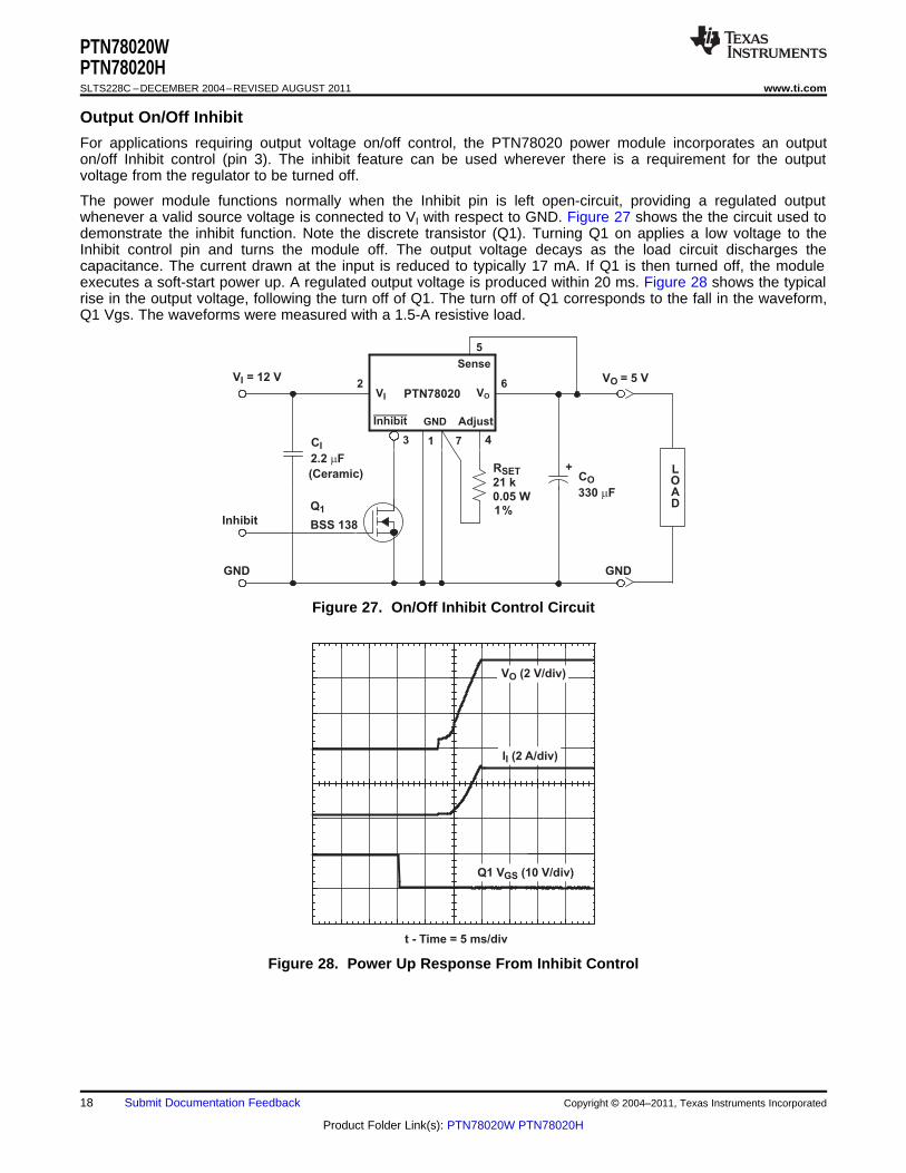
Inhibit
GND GND
1%
(Ceramic)
PTN78020
1 4
62
3
AdjustGND
VOVI
VI = 12 V VO = 5 V
Inhibit
7
5
Sense
+
Q1
BSS 138
LOAD
21 k
CI
2.2 Fm
CO
330 Fm
RSET
0.05 W
t - Time = 5 ms/div
VO (2 V/div)
II (2 A/div)
Q1 VGS (10 V/div)
PTN78020WPTN78020HSLTS228C –DECEMBER 2004–REVISED AUGUST 2011 www.ti.com
Output On/Off Inhibit
For applications requiring output voltage on/off control, the PTN78020 power module incorporates an outputon/off Inhibit control (pin 3). The inhibit feature can be used wherever there is a requirement for the outputvoltage from the regulator to be turned off.
The power module functions normally when the Inhibit pin is left open-circuit, providing a regulated outputwhenever a valid source voltage is connected to VI with respect to GND. Figure 27 shows the the circuit used todemonstrate the inhibit function. Note the discrete transistor (Q1). Turning Q1 on applies a low voltage to theInhibit control pin and turns the module off. The output voltage decays as the load circuit discharges thecapacitance. The current drawn at the input is reduced to typically 17 mA. If Q1 is then turned off, the moduleexecutes a soft-start power up. A regulated output voltage is produced within 20 ms. Figure 28 shows the typicalrise in the output voltage, following the turn off of Q1. The turn off of Q1 corresponds to the fall in the waveform,Q1 Vgs. The waveforms were measured with a 1.5-A resistive load.
Figure 27. On/Off Inhibit Control Circuit
Figure 28. Power Up Response From Inhibit Control
18 Submit Documentation Feedback Copyright © 2004–2011, Texas Instruments Incorporated
Product Folder Link(s): PTN78020W PTN78020H

PTN78020W2 6
5
+7 4
GND Adjust
Sense
13
GNDGND
UDG−06049
VOVI VOVI
Inhibit
C11 µF50 VCeramic
C22.2 µF50 VCeramic(Required)
C3330 µF(Required)
C41 µFCeramicRSET
(2)
(1) (1)
PTN78020WPTN78020H
www.ti.com SLTS228C –DECEMBER 2004–REVISED AUGUST 2011
Optional Input/Output Filters
Power modules include internal input and output ceramic capacitors in all of their designs. However, someapplications require much lower levels of either input reflected or output ripple/noise. This application describesvarious filters and design techniques found to be successful in reducing both input and output ripple/noise.
Input/Output Capacitors
The easiest way to reduce output ripple and noise is to add one or more 1-μF ceramic capacitors, such as C4shown in Figure 29. Ceramic capacitors should be placed close to the output power terminals. A single 1-μFcapacitor reduces the output ripple/noise by 10% to 30% for modules with a rated output current of less than 3 A.(Note: C3 is required to improve the regulator transient response, and does not reduce output ripple and noise.)
Switching regulators draw current from the input line in pulses at their operating frequency. The amount ofreflected (input) ripple/noise generated is directly proportional to the equivalent source impedance of the powersource including the impedance of any input lines. The addition of C1, minimum 2.2-μF ceramic capacitor, nearthe input power pins, reduces reflected conducted ripple/noise by 30% to 50%.
(1) See the specifications for required value and type. For the PTN78020H, C2 = 4 × 4.7 μF.
(2) See the Application Information section for suggeted value and type.
Figure 29. Adding High-Frequency Bypass Capacitors To The Input and Output
π Filters
If a further reduction in ripple/noise level is required for an application, higher order filters must be used. A π (pi)filter, employing a ferrite bead (Fair-Rite part number 2773021447 or equivalent) in series with the input or outputterminals of the regulator reduces the ripple/noise by at least 20 db (see Figure 30 and Figure 31). In order forthe inductor to be effective in reduction of ripple and noise, ceramic capacitors are required. (Note: see CapacitorRecommendations for the PTN78020W for addtional information on vendors and component suggestions.)
These inductors plus ceramic capacitors form an excellent filter because of the rejection at the switchingfrequency (650 kHz - 1 MHz). The placement of this filter is critical. It must be located as close as possible to theinput or output pins to be efffective. The ferrite bead is small (12.5 mm × 3 mm), easy to use, low cost, and haslow dc resistance. Fair-Rite also manufactures a surface mount bead (part number 2773021447), through hole(part number 2673000701) rated to 5 A, but in this application, it is effective to 6 A on the output bus. 1-µH to5-µH inductors can be used in place of the ferrite inductor bead.
Copyright © 2004–2011, Texas Instruments Incorporated Submit Documentation Feedback 19
Product Folder Link(s): PTN78020W PTN78020H

C51 µFCeramic
UDG−06050
C12.2 µF50 VCeramic
C2330 µF50 V(Optional) RSET
C6100 µF
VIVI PTN78020W
2 6
5
+7 4
Vo
Inhibit GND Adjust
Vo
Sense
13
GNDGND
+GND
C32.2 µF50 VCeramic(Required)
C4330 µF(Required)(2)
(3)(4)
L11−5 µH
(1)
L21−5 µH
+
10
15
20
25
30
35
40
45
0 0.5 1 1.5 2 2.5 3
1 MHz
600 kHz
Atte
nuat
ion
− dB
Load Current − A
PTN78020WPTN78020HSLTS228C –DECEMBER 2004–REVISED AUGUST 2011 www.ti.com
(1) See the specifications for required value and type. For the PTN78020H, C3 = 4 × 4.7 μF.
(2) See the Application Information section for suggeted value and type.
(3) Recommended whenever IO > 2A.
(4) For PTN78020H, C1 ≤ 4.7 μF.
Figure 30. Adding π Filters (IO ≤ 3 A)
Figure 31. π-Filter Attenuation vs. Load Current
20 Submit Documentation Feedback Copyright © 2004–2011, Texas Instruments Incorporated
Product Folder Link(s): PTN78020W PTN78020H

C51 µFCeramic
UDG−05089
C11 µF50 VCeramic
C2330 µF50 V(Optional)
RSET
C6100 µF
VIVI
C32.2 µF50 VCeramic(Required)
C4330 µF(Required)
PTN78020W2 6
5
+7 4
Inhibit GND Adjust
Sense
13
GNDGND
+GND
L21 µH to 5 µH
L11 µH to 5 µH
L31 µH to 5 µH
(1)
(2)
(3)(1)
VO
VO
PTN78020WPTN78020H
www.ti.com SLTS228C –DECEMBER 2004–REVISED AUGUST 2011
(1) See the specifications for required value and type. For the PTN78020H, C2 = 4 × 4.7 μF.
(2) See the Application Information section for suggeted value and type.
(3) Recommended whenever IO > 2A.
(4) For PTN78020H, C1 ≥ 4.7 μF.
Figure 32. Adding π Filters (IO = 3 A to 6 A)
Copyright © 2004–2011, Texas Instruments Incorporated Submit Documentation Feedback 21
Product Folder Link(s): PTN78020W PTN78020H

PTN78020WPTN78020HSLTS228C –DECEMBER 2004–REVISED AUGUST 2011 www.ti.com
REVISION HISTORY
Changes from Revision B (APRIL 2008) to Revision C Page
• Added Output Voltage Sense section ............................................................................................................................... 16
22 Submit Documentation Feedback Copyright © 2004–2011, Texas Instruments Incorporated
Product Folder Link(s): PTN78020W PTN78020H

PACKAGE OPTION ADDENDUM
www.ti.com 27-Apr-2017
Addendum-Page 1
PACKAGING INFORMATION
Orderable Device Status(1)
Package Type PackageDrawing
Pins PackageQty
Eco Plan(2)
Lead/Ball Finish(6)
MSL Peak Temp(3)
Op Temp (°C) Device Marking(4/5)
Samples
PTN78020HAH ACTIVE Through-Hole Module
EUK 7 20 RoHS (InWork) & Green
(In Work)
SN N / A for Pkg Type -40 to 85
PTN78020HAS ACTIVE SurfaceMount Module
EUL 7 20 RoHS (InWork) & Green
(In Work)
SNPB Level-1-235C-UNLIM/Level-3-260C-168HRS
-40 to 85
PTN78020HAZ ACTIVE SurfaceMount Module
EUL 7 20 RoHS (InWork) & Green
(In Work)
SNAGCU Level-3-260C-168 HR -40 to 85
PTN78020WAD ACTIVE Through-Hole Module
EUK 7 20 RoHS (InWork) & Green
(In Work)
SN N / A for Pkg Type -40 to 85
PTN78020WAH ACTIVE Through-Hole Module
EUK 7 20 RoHS (InWork) & Green
(In Work)
SN N / A for Pkg Type -40 to 85
PTN78020WAS ACTIVE SurfaceMount Module
EUL 7 20 RoHS (InWork) & Green
(In Work)
SNPB Level-1-235C-UNLIM/Level-3-260C-168HRS
-40 to 85
PTN78020WAZ ACTIVE SurfaceMount Module
EUL 7 20 RoHS (InWork) & Green
(In Work)
SNAGCU Level-3-260C-168 HR -40 to 85
PTN78020WAZT ACTIVE SurfaceMount Module
EUL 7 200 RoHS (InWork) & Green
(In Work)
SNAGCU Level-3-260C-168 HR -40 to 85
(1) The marketing status values are defined as follows:ACTIVE: Product device recommended for new designs.LIFEBUY: TI has announced that the device will be discontinued, and a lifetime-buy period is in effect.NRND: Not recommended for new designs. Device is in production to support existing customers, but TI does not recommend using this part in a new design.PREVIEW: Device has been announced but is not in production. Samples may or may not be available.OBSOLETE: TI has discontinued the production of the device.
(2) RoHS: TI defines "RoHS" to mean semiconductor products that are compliant with the current EU RoHS requirements for all 10 RoHS substances, including the requirement that RoHS substancedo not exceed 0.1% by weight in homogeneous materials. Where designed to be soldered at high temperatures, "RoHS" products are suitable for use in specified lead-free processes. TI mayreference these types of products as "Pb-Free".RoHS Exempt: TI defines "RoHS Exempt" to mean products that contain lead but are compliant with EU RoHS pursuant to a specific EU RoHS exemption.

PACKAGE OPTION ADDENDUM
www.ti.com 27-Apr-2017
Addendum-Page 2
Green: TI defines "Green" to mean the content of Chlorine (Cl) and Bromine (Br) based flame retardants meet JS709B low halogen requirements of <=1000ppm threshold. Antimony trioxide basedflame retardants must also meet the <=1000ppm threshold requirement.
(3) MSL, Peak Temp. - The Moisture Sensitivity Level rating according to the JEDEC industry standard classifications, and peak solder temperature.
(4) There may be additional marking, which relates to the logo, the lot trace code information, or the environmental category on the device.
(5) Multiple Device Markings will be inside parentheses. Only one Device Marking contained in parentheses and separated by a "~" will appear on a device. If a line is indented then it is a continuationof the previous line and the two combined represent the entire Device Marking for that device.
(6) Lead/Ball Finish - Orderable Devices may have multiple material finish options. Finish options are separated by a vertical ruled line. Lead/Ball Finish values may wrap to two lines if the finishvalue exceeds the maximum column width.
Important Information and Disclaimer:The information provided on this page represents TI's knowledge and belief as of the date that it is provided. TI bases its knowledge and belief on informationprovided by third parties, and makes no representation or warranty as to the accuracy of such information. Efforts are underway to better integrate information from third parties. TI has taken andcontinues to take reasonable steps to provide representative and accurate information but may not have conducted destructive testing or chemical analysis on incoming materials and chemicals.TI and TI suppliers consider certain information to be proprietary, and thus CAS numbers and other limited information may not be available for release.
In no event shall TI's liability arising out of such information exceed the total purchase price of the TI part(s) at issue in this document sold by TI to Customer on an annual basis.


IMPORTANT NOTICE
Texas Instruments Incorporated (TI) reserves the right to make corrections, enhancements, improvements and other changes to itssemiconductor products and services per JESD46, latest issue, and to discontinue any product or service per JESD48, latest issue. Buyersshould obtain the latest relevant information before placing orders and should verify that such information is current and complete.TI’s published terms of sale for semiconductor products (http://www.ti.com/sc/docs/stdterms.htm) apply to the sale of packaged integratedcircuit products that TI has qualified and released to market. Additional terms may apply to the use or sale of other types of TI products andservices.Reproduction of significant portions of TI information in TI data sheets is permissible only if reproduction is without alteration and isaccompanied by all associated warranties, conditions, limitations, and notices. TI is not responsible or liable for such reproduceddocumentation. Information of third parties may be subject to additional restrictions. Resale of TI products or services with statementsdifferent from or beyond the parameters stated by TI for that product or service voids all express and any implied warranties for theassociated TI product or service and is an unfair and deceptive business practice. TI is not responsible or liable for any such statements.Buyers and others who are developing systems that incorporate TI products (collectively, “Designers”) understand and agree that Designersremain responsible for using their independent analysis, evaluation and judgment in designing their applications and that Designers havefull and exclusive responsibility to assure the safety of Designers' applications and compliance of their applications (and of all TI productsused in or for Designers’ applications) with all applicable regulations, laws and other applicable requirements. Designer represents that, withrespect to their applications, Designer has all the necessary expertise to create and implement safeguards that (1) anticipate dangerousconsequences of failures, (2) monitor failures and their consequences, and (3) lessen the likelihood of failures that might cause harm andtake appropriate actions. Designer agrees that prior to using or distributing any applications that include TI products, Designer willthoroughly test such applications and the functionality of such TI products as used in such applications.TI’s provision of technical, application or other design advice, quality characterization, reliability data or other services or information,including, but not limited to, reference designs and materials relating to evaluation modules, (collectively, “TI Resources”) are intended toassist designers who are developing applications that incorporate TI products; by downloading, accessing or using TI Resources in anyway, Designer (individually or, if Designer is acting on behalf of a company, Designer’s company) agrees to use any particular TI Resourcesolely for this purpose and subject to the terms of this Notice.TI’s provision of TI Resources does not expand or otherwise alter TI’s applicable published warranties or warranty disclaimers for TIproducts, and no additional obligations or liabilities arise from TI providing such TI Resources. TI reserves the right to make corrections,enhancements, improvements and other changes to its TI Resources. TI has not conducted any testing other than that specificallydescribed in the published documentation for a particular TI Resource.Designer is authorized to use, copy and modify any individual TI Resource only in connection with the development of applications thatinclude the TI product(s) identified in such TI Resource. NO OTHER LICENSE, EXPRESS OR IMPLIED, BY ESTOPPEL OR OTHERWISETO ANY OTHER TI INTELLECTUAL PROPERTY RIGHT, AND NO LICENSE TO ANY TECHNOLOGY OR INTELLECTUAL PROPERTYRIGHT OF TI OR ANY THIRD PARTY IS GRANTED HEREIN, including but not limited to any patent right, copyright, mask work right, orother intellectual property right relating to any combination, machine, or process in which TI products or services are used. Informationregarding or referencing third-party products or services does not constitute a license to use such products or services, or a warranty orendorsement thereof. Use of TI Resources may require a license from a third party under the patents or other intellectual property of thethird party, or a license from TI under the patents or other intellectual property of TI.TI RESOURCES ARE PROVIDED “AS IS” AND WITH ALL FAULTS. TI DISCLAIMS ALL OTHER WARRANTIES ORREPRESENTATIONS, EXPRESS OR IMPLIED, REGARDING RESOURCES OR USE THEREOF, INCLUDING BUT NOT LIMITED TOACCURACY OR COMPLETENESS, TITLE, ANY EPIDEMIC FAILURE WARRANTY AND ANY IMPLIED WARRANTIES OFMERCHANTABILITY, FITNESS FOR A PARTICULAR PURPOSE, AND NON-INFRINGEMENT OF ANY THIRD PARTY INTELLECTUALPROPERTY RIGHTS. TI SHALL NOT BE LIABLE FOR AND SHALL NOT DEFEND OR INDEMNIFY DESIGNER AGAINST ANY CLAIM,INCLUDING BUT NOT LIMITED TO ANY INFRINGEMENT CLAIM THAT RELATES TO OR IS BASED ON ANY COMBINATION OFPRODUCTS EVEN IF DESCRIBED IN TI RESOURCES OR OTHERWISE. IN NO EVENT SHALL TI BE LIABLE FOR ANY ACTUAL,DIRECT, SPECIAL, COLLATERAL, INDIRECT, PUNITIVE, INCIDENTAL, CONSEQUENTIAL OR EXEMPLARY DAMAGES INCONNECTION WITH OR ARISING OUT OF TI RESOURCES OR USE THEREOF, AND REGARDLESS OF WHETHER TI HAS BEENADVISED OF THE POSSIBILITY OF SUCH DAMAGES.Unless TI has explicitly designated an individual product as meeting the requirements of a particular industry standard (e.g., ISO/TS 16949and ISO 26262), TI is not responsible for any failure to meet such industry standard requirements.Where TI specifically promotes products as facilitating functional safety or as compliant with industry functional safety standards, suchproducts are intended to help enable customers to design and create their own applications that meet applicable functional safety standardsand requirements. Using products in an application does not by itself establish any safety features in the application. Designers mustensure compliance with safety-related requirements and standards applicable to their applications. Designer may not use any TI products inlife-critical medical equipment unless authorized officers of the parties have executed a special contract specifically governing such use.Life-critical medical equipment is medical equipment where failure of such equipment would cause serious bodily injury or death (e.g., lifesupport, pacemakers, defibrillators, heart pumps, neurostimulators, and implantables). Such equipment includes, without limitation, allmedical devices identified by the U.S. Food and Drug Administration as Class III devices and equivalent classifications outside the U.S.TI may expressly designate certain products as completing a particular qualification (e.g., Q100, Military Grade, or Enhanced Product).Designers agree that it has the necessary expertise to select the product with the appropriate qualification designation for their applicationsand that proper product selection is at Designers’ own risk. Designers are solely responsible for compliance with all legal and regulatoryrequirements in connection with such selection.Designer will fully indemnify TI and its representatives against any damages, costs, losses, and/or liabilities arising out of Designer’s non-compliance with the terms and provisions of this Notice.
Mailing Address: Texas Instruments, Post Office Box 655303, Dallas, Texas 75265Copyright © 2017, Texas Instruments Incorporated