system-on-chip environment: tutorial - northeastern …specc/sce/sce-tutorial/sce-tutorial.… ·...
TRANSCRIPT
System-on-Chip EnvironmentSCE Version 2.2.0 Beta
Tutorial
Samar AbdiJunyu PengHaobo Yu
Dongwan Shin
Andreas GerstlauerRainer DoemerDaniel Gajski
Center for Embedded Computer SystemsUniversity of California, Irvine
Irvine, CA 92697-3425+1 (949) 824-8919
http://www.cecs.uci.edu
System-on-Chip Environment: SCE Version 2.2.0 Beta; Tutor ialby Samar Abdi, Junyu Peng, Haobo Yu, Dongwan Shin, Andreas Gerstlauer, RainerDoemer, and Daniel Gajski
Center for Embedded Computer SystemsUniversity of California, IrvineIrvine, CA 92697-3425+1 (949) 824-8919http://www.cecs.uci.eduPublished July 23, 2003Copyright © 2003 CECS, UC Irvine
Table of Contents1. Introduction ................................................................................................................1
1.1. Motivation.........................................................................................................11.2. SCE Goals.........................................................................................................21.3. Models for System Design................................................................................21.4. System-on-Chip Environment...........................................................................41.5. Design Example: GSM Vocoder.......................................................................41.6. Organization of the Tutorial..............................................................................5
2. System Specification Analysis...................................................................................92.1. Overview...........................................................................................................92.2. Specification Capture......................................................................................10
2.2.1. SCE window........................................................................................112.2.2. Open project.........................................................................................132.2.3. Open specification model.....................................................................182.2.4. Browse specification model.................................................................242.2.5. View specification model source code.................................................28
2.3. Simulation and Analysis.................................................................................302.3.1. Simulate specification model...............................................................312.3.2. Profile specification model...................................................................382.3.3. Analyze profiling results......................................................................41
2.4. Summary.........................................................................................................483. System Level Design................................................................................................49
3.1. Overview.........................................................................................................493.2. Architecture Exploration.................................................................................51
3.2.1. Try pure software implementation.......................................................523.2.2. Estimate performance..........................................................................663.2.3. Try software/hardware implementation...............................................723.2.4. Estimate performance..........................................................................803.2.5. Generate architecture model................................................................853.2.6. Browse architecture model...................................................................883.2.7. Simulate architecture model (optional)................................................93
3.3. Software Scheduling and RTOS Model Insertion...........................................963.3.1. Serialize behaviors...............................................................................973.3.2. Generate serialized model..................................................................1063.3.3. Simulate serialized model (optional).................................................110
3.4. Communication Synthesis............................................................................1133.4.1. Select bus protocols...........................................................................1143.4.2. Map channels to buses.......................................................................1173.4.3. Generate communication model........................................................119
iii

3.4.4. Browse communication model..........................................................1333.4.5. Simulate communication model (optional)........................................137
3.5. Summary.......................................................................................................1404. Custom Hardware Design.....................................................................................141
4.1. Overview.......................................................................................................1414.2. RTL Preprocessing........................................................................................143
4.2.1. View behavioral input model.............................................................1444.2.2. Generate SFSMD model....................................................................1474.2.3. Browse SFSMD model......................................................................1504.2.4. View SFSMD model (optional).........................................................1524.2.5. Simulate SFSMD model (optional)...................................................1554.2.6. Analyze SFSMD model.....................................................................158
4.3. RTL Allocation.............................................................................................1654.3.1. Allocate functional units....................................................................1664.3.2. Allocate storage units.........................................................................1724.3.3. Allocate buses....................................................................................178
4.4. RTL Scheduling and Binding........................................................................1874.4.1. Schedule and bind manually (optional).............................................1884.4.2. Schedule and bind automatically.......................................................200
4.5. RTL Refinement............................................................................................2064.5.1. Generate RTL model..........................................................................2074.5.2. Browse RTL model............................................................................2124.5.3. View RTL model (optional)...............................................................2144.5.4. View Verilog RTL model (optional)..................................................2174.5.5. Simulate RTL model (optional).........................................................219
4.6. Summary.......................................................................................................2225. Embedded Software Design..................................................................................223
5.1. Overview.......................................................................................................2235.2. SW code generation......................................................................................224
5.2.1. Generate C code.................................................................................2255.2.2. Browse and View C code...................................................................2295.2.3. Simulate C model (optional)..............................................................230
5.3. Instruction set simulation..............................................................................2335.3.1. Import instruction set simulator model..............................................2345.3.2. Simulate cycle accurate model...........................................................239
5.4. Summary.......................................................................................................2446. Conclusion..............................................................................................................245A. Frequently Asked Questions................................................................................247References...................................................................................................................251
iv
Chapter 1. Introduction
The basic purpose of this tutorial is to guide a user through our System-on-Chip designenvironment (SCE). SCE helps designers to take an abstract functional description ofthe design and produce an implementation. We begin with a brief overview of our SoCmethodology by describing the design flow and various abstraction levels. The overviewalso covers the user interfaces and the tools that support the design flow.
We then describe the example that we use throughout this tutorial. We selected the GSMVocoder as an example for a variety of reasons. For one, the Vocoder is a fairly largedesign and is an apt representative of a typical component ofa System-on-Chip design.Moreover, the functional specification of the Vocoder is well defined and publicly avail-able from the European Telecommunication Standards Institute (ETSI).
The tutorial gives a step by step illustration of using the System-on-Chip Environment.Screenshots of the GUI are presented to aid the user in using the various features ofSCE. (Please note that, depending on your specific version ofthe System-on-Chip Envi-ronment SCE and your system settings, the screen shots shownin this document may beslightly different from the actual display on your screen.)Over the course of this chap-ter, the user is guided on synthesizing the Vocoder model from an abstract specificationto a clock cycle accurate implementation. The screenshots at each design step are sup-plemented with brief observations and the rationale for making design decisions. Thiswould help the designer to gain an insight into the design process instead of merely fol-lowing the steps. We wind up the tutorial with a conclusion and references. This tutorialassumes that the readers of this tutorial have basic knowledge of system design tasksand flow. In case the reader feels difficulty going following this tutorial, he can alwaysgo to the Appendix A: FAQ (Frequently Asked Questions) at theend of the tutorial toseek more explanation.
1.1. MotivationSystem-on-Chip capability introduces new challenges in the design process. For one,co-design becomes a crucial issue. Software and Hardware must be developed together.However, both Software and Hardware designers have different views of the system andthey use different design and modeling techniques.
Secondly, the process of system design from specification tomask is long and elaborate.The process must therefore be split into several steps. At each design step, models mustbe written and relevant properties must be verified.
1
Chapter 1. Introduction
Thirdly, the system designers are not particularly fond of having to learn different lan-guages. Moreover, writing different models and validatingthem for each step in thedesign process is a huge overkill. Designers prefer to create solutions rather than writeseveral models to verify their designs.
It is with these aspects and challenges in mind that we have come up with a System-on-Chip Environment that takes off the drudgery of manual repetitive work from thedesigners by generating each successive model automatically according to the decisionsmade by the designers.
1.2. SCE GoalsSCE represents a new technology that allows designers to capture system specificationas a composition of C-functions. These are automatically refined into different modelsrequired at each step of the design process. Therefore designers can devote more effortto the creative part of designing and the tools can create models for validation and syn-thesis. The end result is that the designers do not need to learn new system level designlanguages (SystemC, SpecC, Superlog, etc.) or even the existing Hardware DescriptionLanguages (Verilog, VHDL).
Consequently, the designers have to enter only the golden specification of the design andmake design decisions interactively in SCE. The models for simulation, synthesis andverification are generated automatically.
2
Chapter 1. Introduction
1.3. Models for System Design
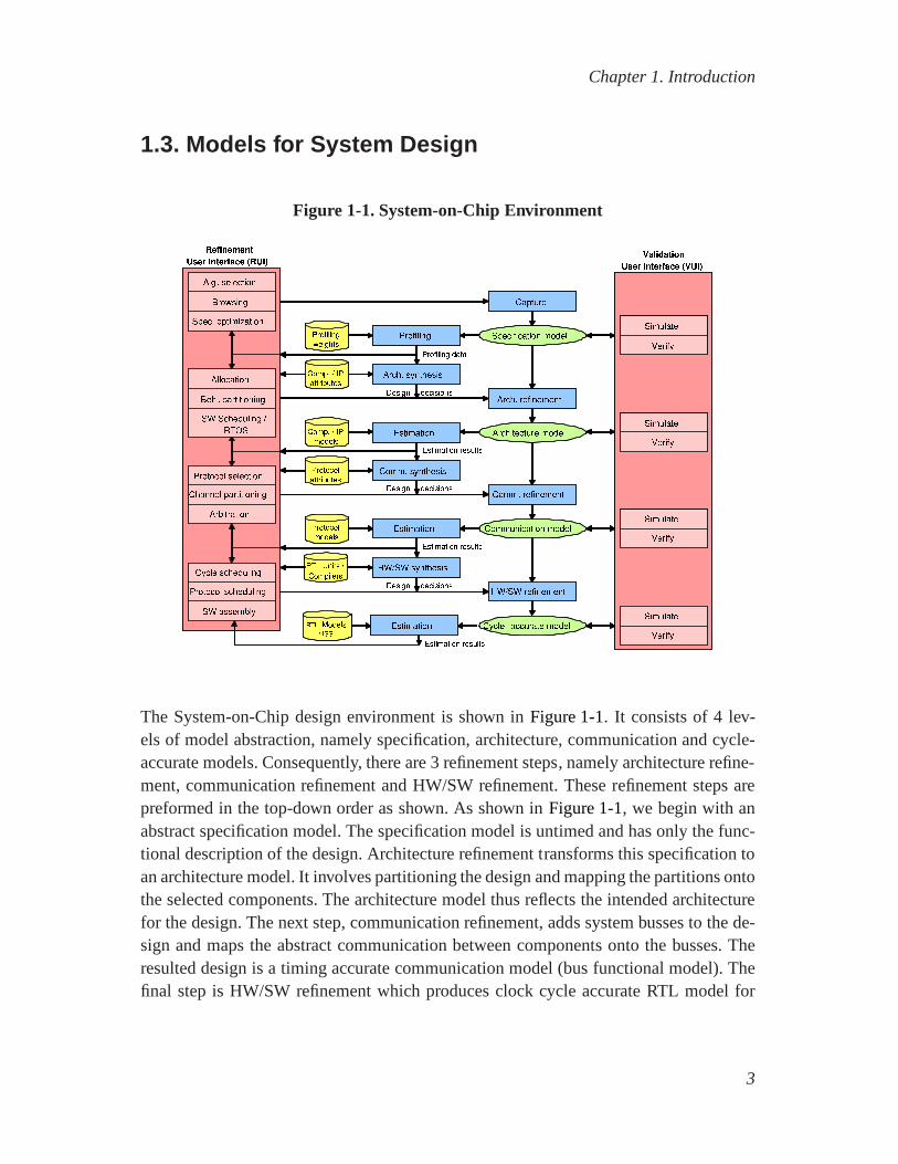
Figure 1-1. System-on-Chip Environment
The System-on-Chip design environment is shown inFigure 1-1. It consists of 4 lev-els of model abstraction, namely specification, architecture, communication and cycle-accurate models. Consequently, there are 3 refinement steps, namely architecture refine-ment, communication refinement and HW/SW refinement. These refinement steps arepreformed in the top-down order as shown. As shown inFigure 1-1, we begin with anabstract specification model. The specification model is untimed and has only the func-tional description of the design. Architecture refinement transforms this specification toan architecture model. It involves partitioning the designand mapping the partitions ontothe selected components. The architecture model thus reflects the intended architecturefor the design. The next step, communication refinement, adds system busses to the de-sign and maps the abstract communication between components onto the busses. Theresulted design is a timing accurate communication model (bus functional model). Thefinal step is HW/SW refinement which produces clock cycle accurate RTL model for
3
Chapter 1. Introduction
the hardware components and instruction set specific assembly code for the processors.All models have well defined semantics, are executable and can be validated throughsimulation.
1.4. System-on-Chip EnvironmentThe SCE provides an environment for modeling, synthesis andvalidation. It includes agraphical user interface (GUI) and a set of tools to facilitate the design flow and performthe aforementioned refinement steps. The two major components of the GUI are theRefinement User Interface (RUI) on the left and the Validation User Interface (VUI) onthe right as shown inFigure 1-1. The RUI allows designers to make and input designdecisions, such as component allocation, specification mapping. With design decisionsmade, refinement tools can be invoked inside RUI to refine models. The VUI allows thesimulation of all models to validate the design at each stageof the design flow.
Each of the boxes corresponds to a tool which performs a specific task automatically.A profiling tool is used to obtain the characteristics of the initial specification, whichserves as the basis for architecture exploration. The refinement tool set automaticallytransforms models based on relevant design decisions. The estimation tool set producesquality metrics for each intermediate models, which can be evaluated by designers.
With the assistance of the GUI and tool set, it is relatively easy for designer to stepthrough the design process. With the editing, browsing and algorithm selection capa-bility provided by RUI, a specification model can be efficiently captured by designers.Based on the information profiled on the specification, designers input architectural de-cisions and apply the architecture refinement tool to derivethe architecture model. If theestimated metrics are satisfactory, designers can focus oncommunication issues, suchas protocol selection and channel partitioning. With communication decisions made, thecommunication refinement tool is used to generate the communication model. Finally,the implementation model is produced in the similar fashion. The implementation modelis ready for RTL synthesis.
We are currently in the process of developing tools for automating the synthesis tasksfor system level design shown in the exploration engine. Thetutorial presents automaticRTL synthesis. The next challenge is to automatically perform architecture and commu-nication synthesis.
4
Chapter 1. Introduction
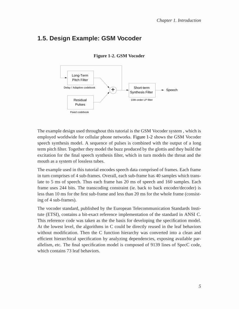
1.5. Design Example: GSM Vocoder
Figure 1-2. GSM Vocoder
Short-termSynthesis Filter
Long-TermPitch Filter
ResidualPulses
+ Speech
Fixed codebook
10th-order LP filter
Delay / Adaptive codebook
The example design used throughout this tutorial is the GSM Vocoder system , which isemployed worldwide for cellular phone networks.Figure 1-2shows the GSM Vocoderspeech synthesis model. A sequence of pulses is combined with the output of a longterm pitch filter. Together they model the buzz produced by the glottis and they build theexcitation for the final speech synthesis filter, which in turn models the throat and themouth as a system of lossless tubes.
The example used in this tutorial encodes speech data comprised of frames. Each framein turn comprises of 4 sub-frames. Overall, each sub-frame has 40 samples which trans-late to 5 ms of speech. Thus each frame has 20 ms of speech and 160 samples. Eachframe uses 244 bits. The transcoding constraint (ie. back toback encoder/decoder) isless than 10 ms for the first sub-frame and less than 20 ms for the whole frame (consist-ing of 4 sub-frames).
The vocoder standard, published by the European Telecommunication Standards Insti-tute (ETSI), contains a bit-exact reference implementation of the standard in ANSI C.This reference code was taken as the the basis for developingthe specification model.At the lowest level, the algorithms in C could be directly reused in the leaf behaviorswithout modification. Then the C function hierarchy was converted into a clean andefficient hierarchical specification by analyzing dependencies, exposing available par-allelism, etc. The final specification model is composed of 9139 lines of SpecC code,which contains 73 leaf behaviors.
5
Chapter 1. Introduction
1.6. Organization of the Tutorial
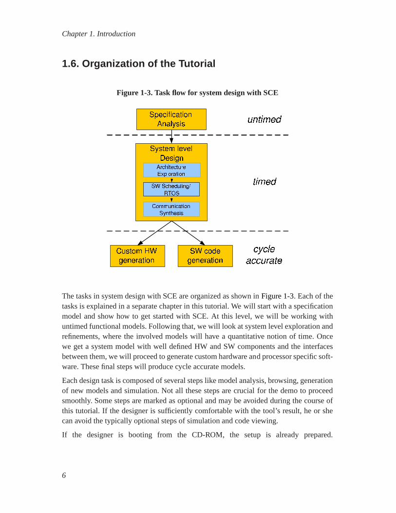
Figure 1-3. Task flow for system design with SCE
The tasks in system design with SCE are organized as shown inFigure 1-3. Each of thetasks is explained in a separate chapter in this tutorial. Wewill start with a specificationmodel and show how to get started with SCE. At this level, we will be working withuntimed functional models. Following that, we will look at system level exploration andrefinements, where the involved models will have a quantitative notion of time. Oncewe get a system model with well defined HW and SW components andthe interfacesbetween them, we will proceed to generate custom hardware and processor specific soft-ware. These final steps will produce cycle accurate models.
Each design task is composed of several steps like model analysis, browsing, generationof new models and simulation. Not all these steps are crucialfor the demo to proceedsmoothly. Some steps are marked as optional and may be avoided during the course ofthis tutorial. If the designer is sufficiently comfortable with the tool’s result, he or shecan avoid the typically optional steps of simulation and code viewing.
If the designer is booting from the CD-ROM, the setup is already prepared.
6

Chapter 1. Introduction
Otherwise, the designer may follow the following steps to set up the demo. Startwith a new shell of your choice. If you are working with a c-shell, run "source$SCE_INSTALLATION_PATH/bin/setup.csh". If you are working with bourne shell,run "$SCE_INSTALLATION_PATH/bin/setup.sh". Now run "setup_demo" to setup thedemonstration in the current directory. This will add some new files to be used duringthe demo.
Acknowledgment:
The authors would like to thank Tsuneo Kinoshita of NASDA, Japan for his patience ingoing through the tutorial and helping us make it more understandable and comprehen-sive. We would also like to thank Yoshihisa Kojima of the University of Tokyo for hishelp in uncovering several mistakes in the tutorial’s text.
7

Chapter 1. Introduction
8
Chapter 2. System Specification Analysis
2.1. Overview
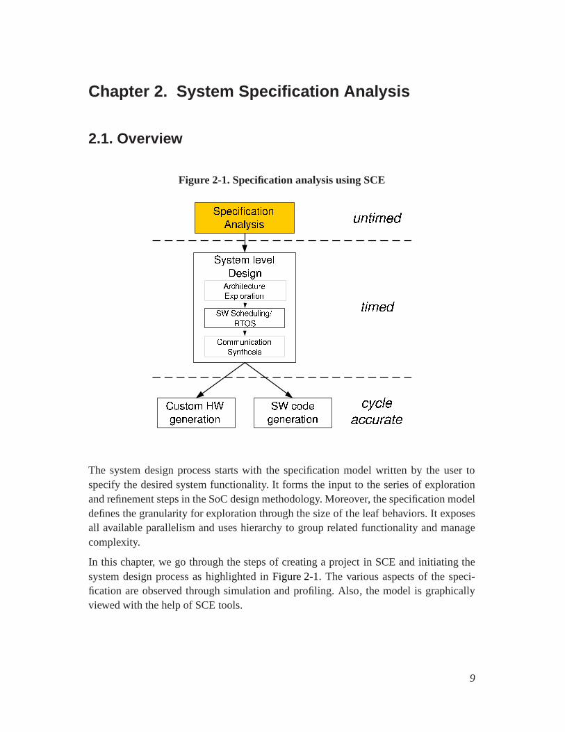
Figure 2-1. Specification analysis using SCE
The system design process starts with the specification model written by the user tospecify the desired system functionality. It forms the input to the series of explorationand refinement steps in the SoC design methodology. Moreover, the specification modeldefines the granularity for exploration through the size of the leaf behaviors. It exposesall available parallelism and uses hierarchy to group related functionality and managecomplexity.
In this chapter, we go through the steps of creating a projectin SCE and initiating thesystem design process as highlighted inFigure 2-1. The various aspects of the speci-fication are observed through simulation and profiling. Also, the model is graphicallyviewed with the help of SCE tools.
9
Chapter 2. System Specification Analysis
2.2. Specification CaptureThe system design process starts with the specification model written by the user tospecify the desired system functionality. It forms the input to the series of explorationand refinement steps in the SoC design methodology. Moreover, the specification modeldefines the granularity for exploration through the size of the leaf behaviors. It exposesall available parallelism and uses hierarchy to group related functionality and managecomplexity.
In this section, we go through the steps of creating a projectin SCE and initiating thesystem design process. The various aspects of the specification are observed throughsimulation and profiling. Also, the model is graphically viewed with the help of SCEtools.
The models that we will deal with in this phase of system design are untimed functionalmodels. The tasks of the system specification, referred to asbehaviors in our parlance,follow a causal order of execution. The main idea in this section is to introduce the userto the SCE GUI and to demonstrate the capability of graphically viewing the behaviorsand their organization in the specification model.
10
Chapter 2. System Specification Analysis
2.2.1. SCE window
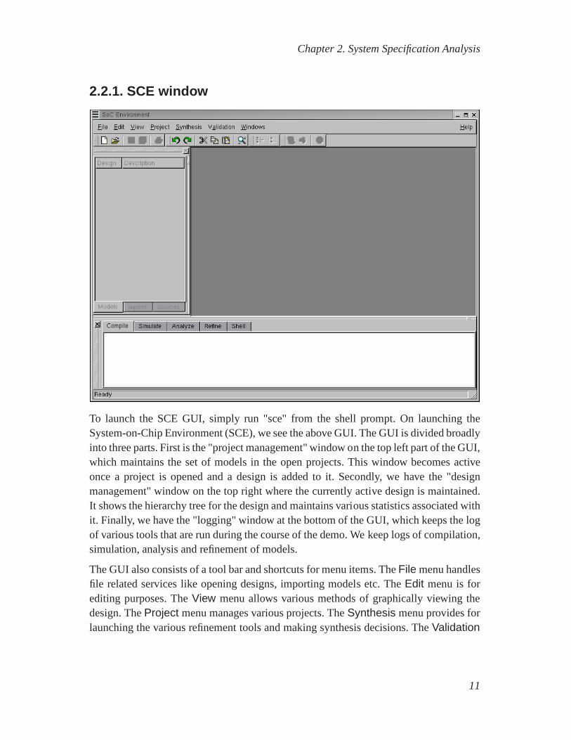
To launch the SCE GUI, simply run "sce" from the shell prompt.On launching theSystem-on-Chip Environment (SCE), we see the above GUI. TheGUI is divided broadlyinto three parts. First is the "project management" window on the top left part of the GUI,which maintains the set of models in the open projects. This window becomes activeonce a project is opened and a design is added to it. Secondly,we have the "designmanagement" window on the top right where the currently active design is maintained.It shows the hierarchy tree for the design and maintains various statistics associated withit. Finally, we have the "logging" window at the bottom of theGUI, which keeps the logof various tools that are run during the course of the demo. Wekeep logs of compilation,simulation, analysis and refinement of models.
The GUI also consists of a tool bar and shortcuts for menu items. TheFile menu handlesfile related services like opening designs, importing models etc. TheEdit menu is forediting purposes. TheView menu allows various methods of graphically viewing thedesign. TheProject menu manages various projects. TheSynthesis menu provides forlaunching the various refinement tools and making synthesisdecisions. TheValidation
11

Chapter 2. System Specification Analysis
menu is primarily for compiling or simulating models.
12
Chapter 2. System Specification Analysis
2.2.2. Open project
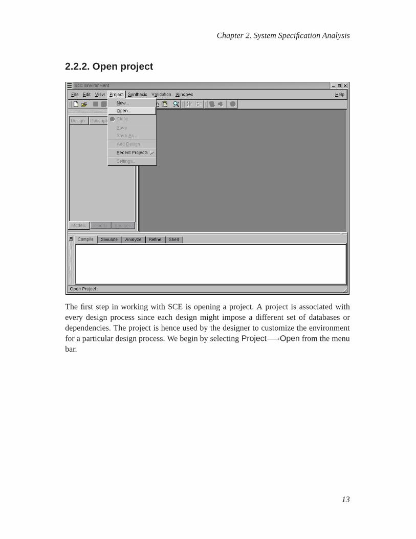
The first step in working with SCE is opening a project. A project is associated withevery design process since each design might impose a different set of databases ordependencies. The project is hence used by the designer to customize the environmentfor a particular design process. We begin by selectingProject−→Open from the menubar.
13
Chapter 2. System Specification Analysis
2.2.2.1. Open project (cont’d)
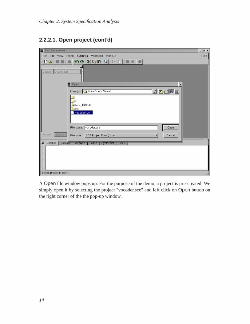
A Open file window pops up. For the purpose of the demo, a project is pre-created. Wesimply open it by selecting the project "vocoder.sce" and left click on Open button onthe right corner of the the pop-up window.
14

Chapter 2. System Specification Analysis
2.2.2.2. Open project (cont’d)
Since we need to ensure that the paths to dependencies are correctly set, we now checkthe settings for this precreated "vocoder.sce" project by selectingProject−→Settings...from the top menu bar.
15

Chapter 2. System Specification Analysis
2.2.2.3. Open project (cont’d)
We now see the compiler settings showing the import path for the model’s libraries andthe ’-v’ (verbose) option. TheInclude path setting gives the path which is searchedfor header files. TheImport path is searched for files imported into the model. TheLibrary path is used for looking up the libraries used during compilation. There arealso settings provided for specifying which libraries to link against, which macros todefine and which to undefine. These settings basically form the compilation command.To check the simulator settings, left click on theSimulator tab.
16

Chapter 2. System Specification Analysis
2.2.2.4. Open project (cont’d)
We now see the simulator settings showing the simulation command for the"vocoder.sce" project. There are settings available to direct the output of the modelsimulation. As can be seen, the simulation output may be directed to a terminal, loggedto a file or dumped to an external console. For the demo, we direct the output of thesimulation to an xterm. Also note that the simulation command may be specified in thesettings. This command is invoked when the model is validated after compilation. Thevocoder simulation processes 163 frames of speech and the output is matched against agolden file. PressOK to proceed.
17
Chapter 2. System Specification Analysis
2.2.3. Open specification model
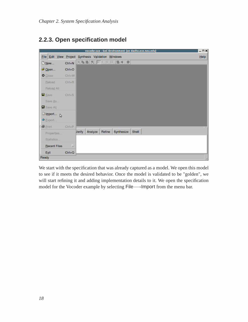
We start with the specification that was already captured as amodel. We open this modelto see if it meets the desired behavior. Once the model is validated to be "golden", wewill start refining it and adding implementation details to it. We open the specificationmodel for the Vocoder example by selectingFile−→Import from the menu bar.
18
Chapter 2. System Specification Analysis
2.2.3.1. Open specification model (cont’d)
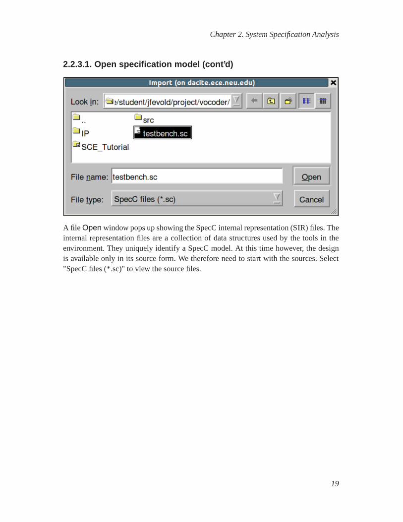
A file Open window pops up showing the SpecC internal representation (SIR) files. Theinternal representation files are a collection of data structures used by the tools in theenvironment. They uniquely identify a SpecC model. At this time however, the designis available only in its source form. We therefore need to start with the sources. Select"SpecC files (*.sc)" to view the source files.
19
Chapter 2. System Specification Analysis
2.2.3.2. Open specification model (cont’d)
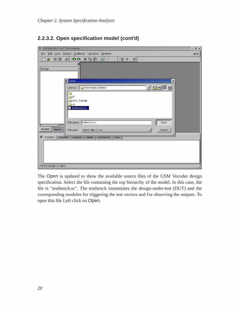
The Open is updated to show the available source files of the GSM Vocoder designspecification. Select the file containing the top hierarchy of the model. In this case, thefile is "testbench.sc". The testbench instantiates the design-under-test (DUT) and thecorresponding modules for triggering the test vectors and for observing the outputs. Toopen this file Left click onOpen.
20
Chapter 2. System Specification Analysis
2.2.3.3. Open specification model (cont’d)
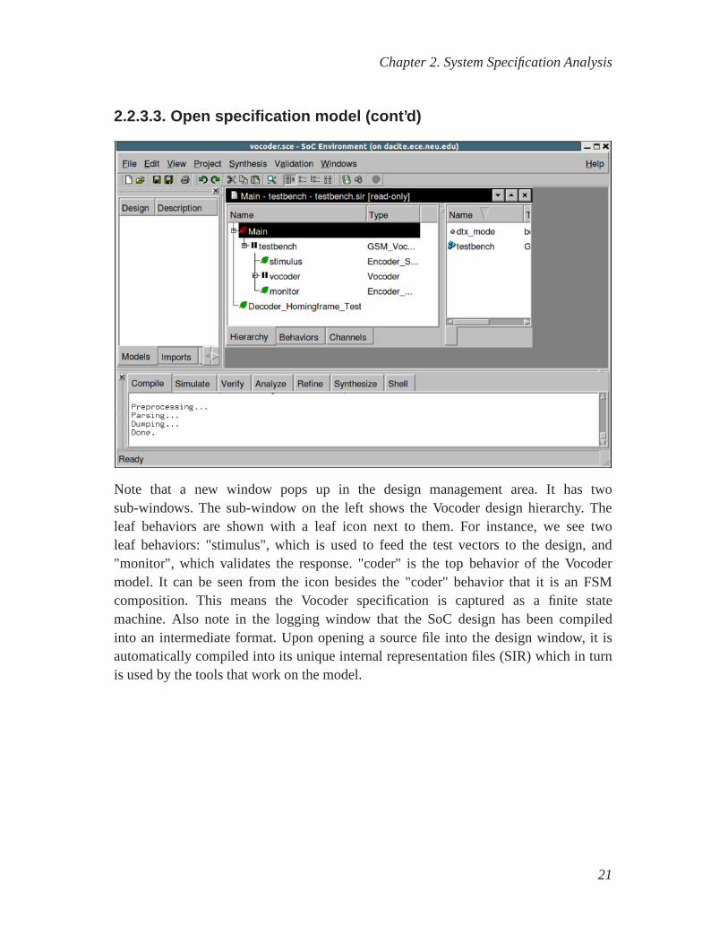
Note that a new window pops up in the design management area. It has twosub-windows. The sub-window on the left shows the Vocoder design hierarchy. Theleaf behaviors are shown with a leaf icon next to them. For instance, we see twoleaf behaviors: "stimulus", which is used to feed the test vectors to the design, and"monitor", which validates the response. "coder" is the topbehavior of the Vocodermodel. It can be seen from the icon besides the "coder" behavior that it is an FSMcomposition. This means the Vocoder specification is captured as a finite statemachine. Also note in the logging window that the SoC design has been compiledinto an intermediate format. Upon opening a source file into the design window, it isautomatically compiled into its unique internal representation files (SIR) which in turnis used by the tools that work on the model.
21
Chapter 2. System Specification Analysis
2.2.3.4. Open specification model (cont’d)
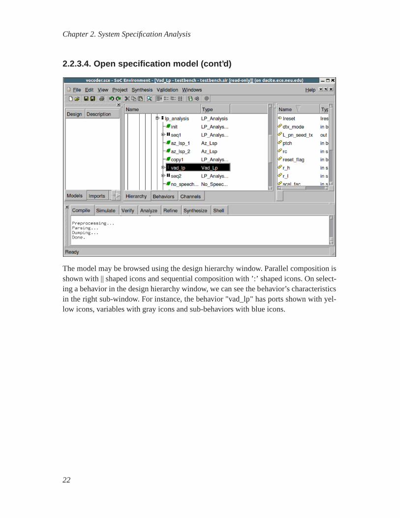
The model may be browsed using the design hierarchy window. Parallel composition isshown with || shaped icons and sequential composition with ’:’ shaped icons. On select-ing a behavior in the design hierarchy window, we can see the behavior’s characteristicsin the right sub-window. For instance, the behavior "vad_lp" has ports shown with yel-low icons, variables with gray icons and sub-behaviors withblue icons.
22
Chapter 2. System Specification Analysis
2.2.3.5. Open specification model (cont’d)
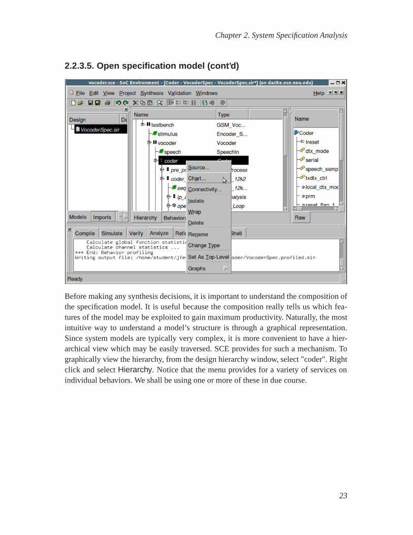
Before making any synthesis decisions, it is important to understand the composition ofthe specification model. It is useful because the composition really tells us which fea-tures of the model may be exploited to gain maximum productivity. Naturally, the mostintuitive way to understand a model’s structure is through agraphical representation.Since system models are typically very complex, it is more convenient to have a hier-archical view which may be easily traversed. SCE provides for such a mechanism. Tographically view the hierarchy, from the design hierarchy window, select "coder". Rightclick and selectHierarchy. Notice that the menu provides for a variety of services onindividual behaviors. We shall be using one or more of these in due course.
23
Chapter 2. System Specification Analysis
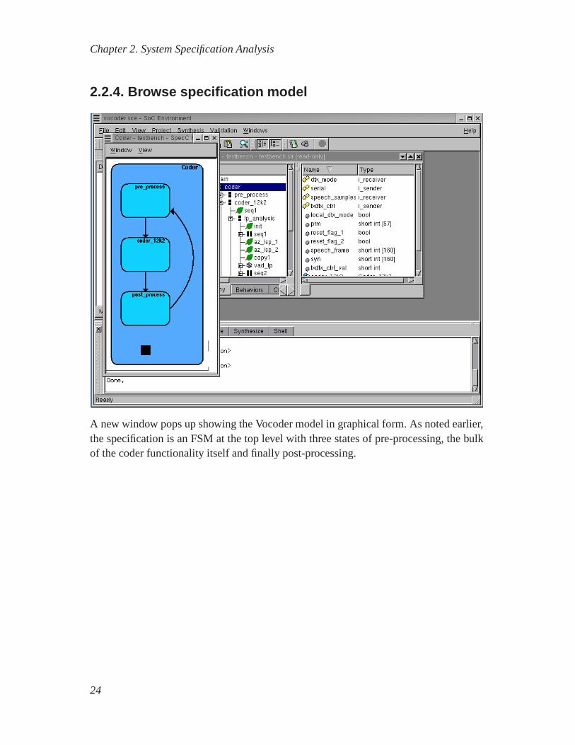
2.2.4. Browse specification model
A new window pops up showing the Vocoder model in graphical form. As noted earlier,the specification is an FSM at the top level with three states of pre-processing, the bulkof the coder functionality itself and finally post-processing.
24
Chapter 2. System Specification Analysis
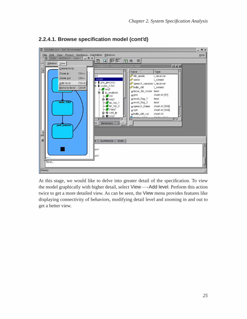
2.2.4.1. Browse specification model (cont’d)
At this stage, we would like to delve into greater detail of the specification. To viewthe model graphically with higher detail, selectView−→Add level. Perform this actiontwice to get a more detailed view. As can be seen, theView menu provides features likedisplaying connectivity of behaviors, modifying detail level and zooming in and out toget a better view.
25
Chapter 2. System Specification Analysis
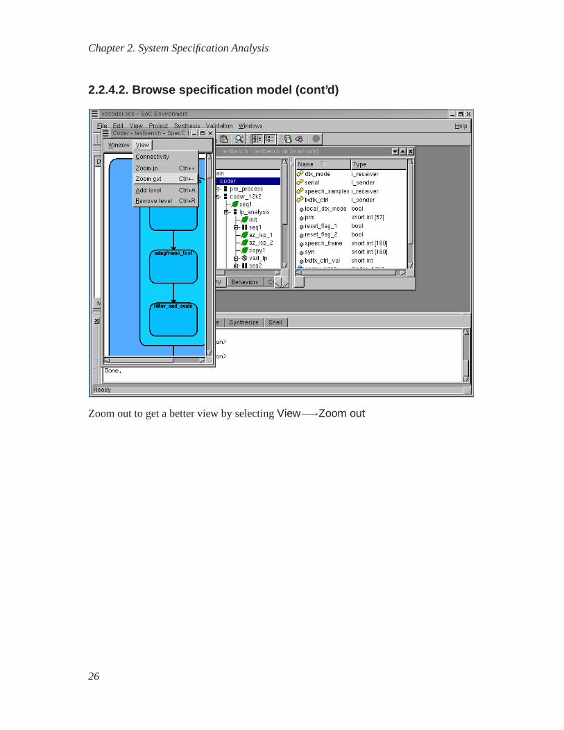
2.2.4.2. Browse specification model (cont’d)
Zoom out to get a better view by selectingView−→Zoom out
26
Chapter 2. System Specification Analysis
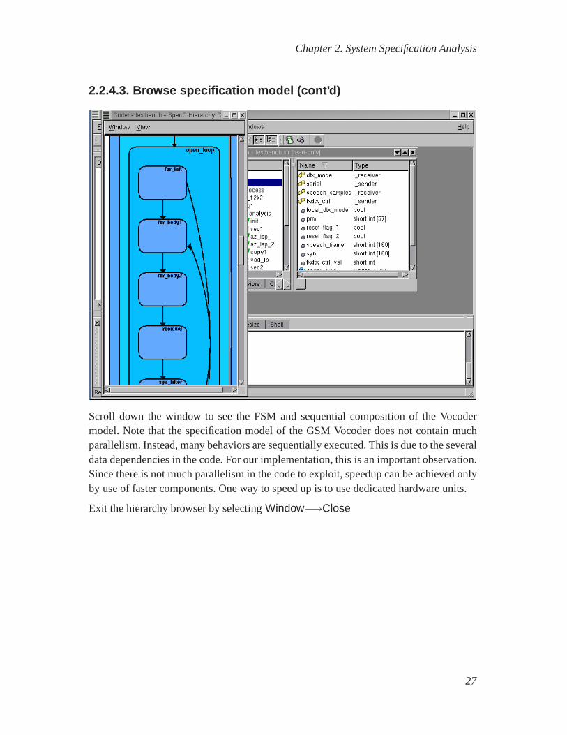
2.2.4.3. Browse specification model (cont’d)
Scroll down the window to see the FSM and sequential composition of the Vocodermodel. Note that the specification model of the GSM Vocoder does not contain muchparallelism. Instead, many behaviors are sequentially executed. This is due to the severaldata dependencies in the code. For our implementation, thisis an important observation.Since there is not much parallelism in the code to exploit, speedup can be achieved onlyby use of faster components. One way to speed up is to use dedicated hardware units.
Exit the hierarchy browser by selectingWindow−→Close
27
Chapter 2. System Specification Analysis
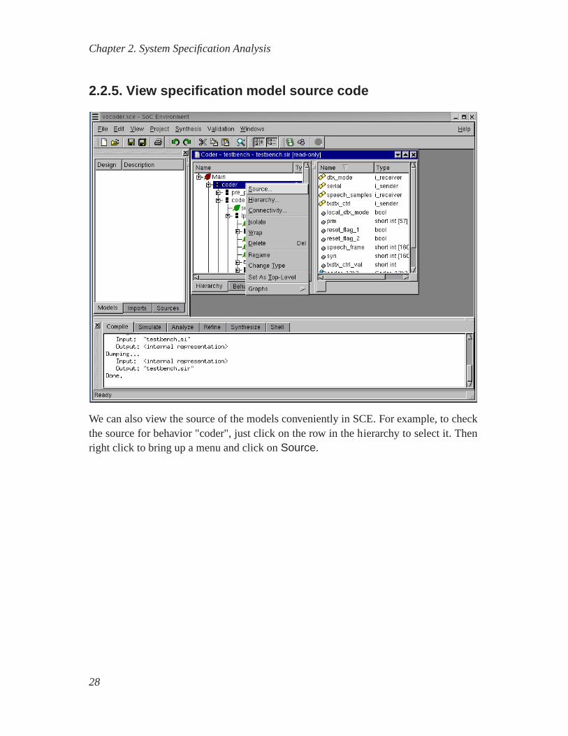
2.2.5. View specification model source code
We can also view the source of the models conveniently in SCE.For example, to checkthe source for behavior "coder", just click on the row in the hierarchy to select it. Thenright click to bring up a menu and click onSource.
28
Chapter 2. System Specification Analysis
2.2.5.1. View specification model source code(cont’d)
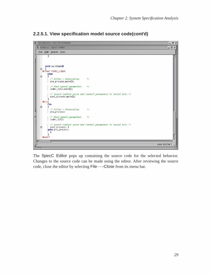
The SpecC Editor pops up containing the source code for the selected behavior.Changes to the source code can be made using the editor. Afterreviewing the sourcecode, close the editor by selectingFile−→Close from its menu bar.
29
Chapter 2. System Specification Analysis
2.3. Simulation and AnalysisOnce we have captured the specification as a model and browsedthrough its behavioralhierarchy and connectivity, we need to ensure that our specification is correct. We alsoneed to analyze our specification model to derive interesting observations about the na-ture of the computation. The check for correctness is done bysimulating the model.Note that the model is purely functional, so the simulation runs very quickly. This isalso a good time to debug the model for functional errors thatmight have crept in whilewriting it.
After the model is verified to be functionally correct, we proceed to the analysis phase.For this, we need to profile the model using the profiling tool available in SCE. Theprofile gives us useful information like the about of computation, its distribution overthe various behaviors in the model and its nature. This information is need to makecrucial architectural choices as we will see as the demo proceeds.
30
Chapter 2. System Specification Analysis
2.3.1. Simulate specification model
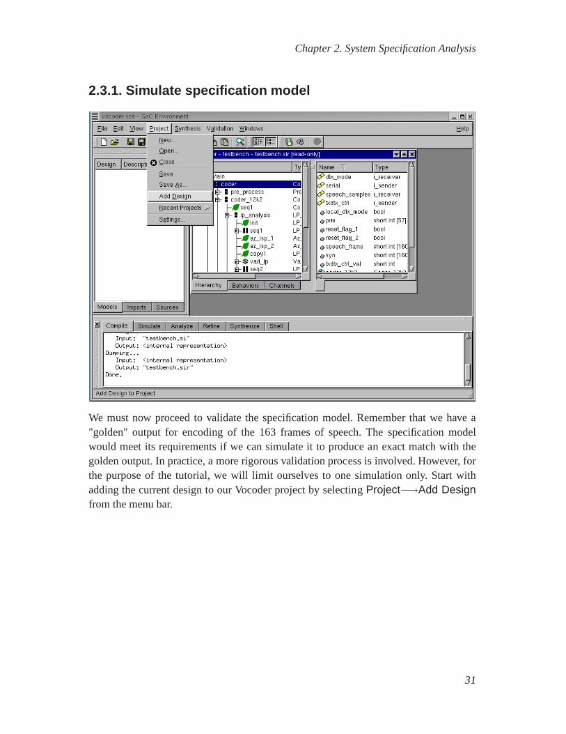
We must now proceed to validate the specification model. Remember that we have a"golden" output for encoding of the 163 frames of speech. Thespecification modelwould meet its requirements if we can simulate it to produce an exact match with thegolden output. In practice, a more rigorous validation process is involved. However, forthe purpose of the tutorial, we will limit ourselves to one simulation only. Start withadding the current design to our Vocoder project by selecting Project−→Add Designfrom the menu bar.
31

Chapter 2. System Specification Analysis
2.3.1.1. Simulate specification model (cont’d)
The project is now added as seen in the project management workspace on the left in theGUI.
32

Chapter 2. System Specification Analysis
2.3.1.2. Simulate specification model (cont’d)
We must now rename the project to have a suitable name. Remember that our method-ology involved 4 models at different levels of abstraction.As these new models areproduced, we need to keep track of them. Right click on "testbench.sir" and selectRe-name to rename the design to "VocoderSpec". This indicates that the current modelcorresponds to the topmost level of abstraction, namely thespecification level. Note thatthe extension ".sir" would be automatically appended. Alsonote that a model may bemade activated, deleted, renamed and and its description modified by right click on itsname in the project management window.
33
Chapter 2. System Specification Analysis
2.3.1.3. Simulate specification model (cont’d)
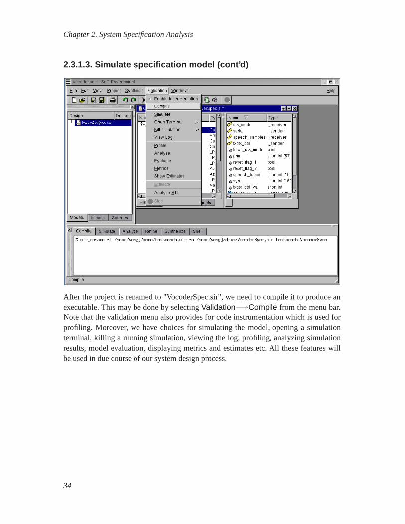
After the project is renamed to "VocoderSpec.sir", we need to compile it to produce anexecutable. This may be done by selectingValidation−→Compile from the menu bar.Note that the validation menu also provides for code instrumentation which is used forprofiling. Moreover, we have choices for simulating the model, opening a simulationterminal, killing a running simulation, viewing the log, profiling, analyzing simulationresults, model evaluation, displaying metrics and estimates etc. All these features willbe used in due course of our system design process.
34
Chapter 2. System Specification Analysis
2.3.1.4. Simulate specification model (cont’d)
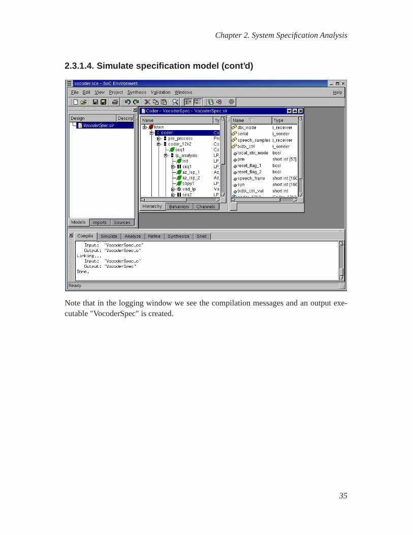
Note that in the logging window we see the compilation messages and an output exe-cutable "VocoderSpec" is created.
35
Chapter 2. System Specification Analysis
2.3.1.5. Simulate specification model (cont’d)
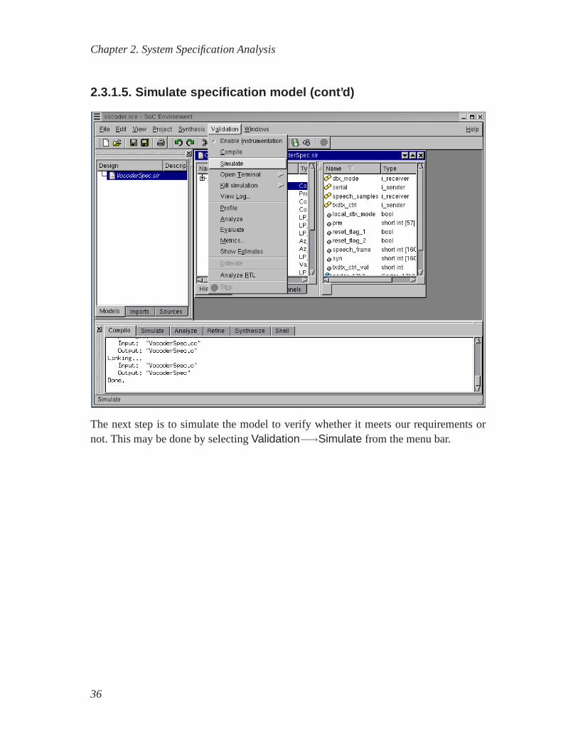
The next step is to simulate the model to verify whether it meets our requirements ornot. This may be done by selectingValidation−→Simulate from the menu bar.
36

Chapter 2. System Specification Analysis
2.3.1.6. Simulate specification model (cont’d)
Note that an xterm pops up showing the simulation of the Vocoder specification modelon a 163 frame speech sample. The simulation should finish correctly which is indicatedby the exit status being ’0’. It can be seen that 163 speech frames were correctly simu-lated and the resulting bit file matches the one given with thevocoder standard. It may benoted that each frame has an encoding delay of 0 ms. This is a because our specificationmodel has no notion of timing. As explained in the methodology, the specification is apurely functional representation of the design and is devoid of timing. For this reason,all behaviors in the model execute in 0 time thereby giving anencoding delay of 0 foreach frame. Press RETURN to close this window and proceed to the next step.
37
Chapter 2. System Specification Analysis
2.3.2. Profile specification model
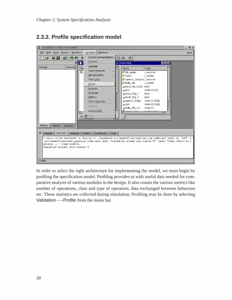
In order to select the right architecture for implementing the model, we must begin byprofiling the specification model. Profiling provides us withuseful data needed for com-parative analysis of various modules in the design. It also counts the various metrics likenumber of operations, class and type of operation, data exchanged between behaviorsetc. These statistics are collected during simulation. Profiling may be done by selectingValidation−→Profile from the menu bar.
38
Chapter 2. System Specification Analysis
2.3.2.1. Profile specification model (cont’d)
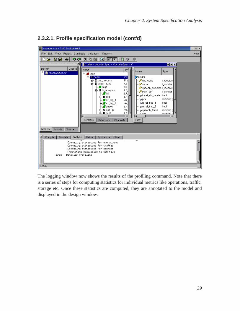
The logging window now shows the results of the profiling command. Note that thereis a series of steps for computing statistics for individualmetrics like operations, traffic,storage etc. Once these statistics are computed, they are annotated to the model anddisplayed in the design window.
39
Chapter 2. System Specification Analysis
2.3.2.2. Profile specification model (cont’d)
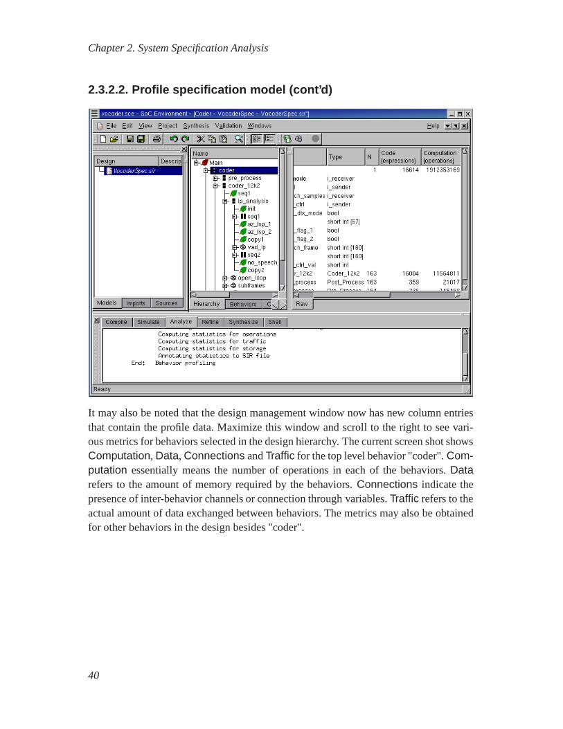
It may also be noted that the design management window now hasnew column entriesthat contain the profile data. Maximize this window and scroll to the right to see vari-ous metrics for behaviors selected in the design hierarchy.The current screen shot showsComputation, Data, Connections andTraffic for the top level behavior "coder".Com-putation essentially means the number of operations in each of the behaviors.Datarefers to the amount of memory required by the behaviors.Connections indicate thepresence of inter-behavior channels or connection throughvariables.Traffic refers to theactual amount of data exchanged between behaviors. The metrics may also be obtainedfor other behaviors in the design besides "coder".
40
Chapter 2. System Specification Analysis
2.3.3. Analyze profiling results
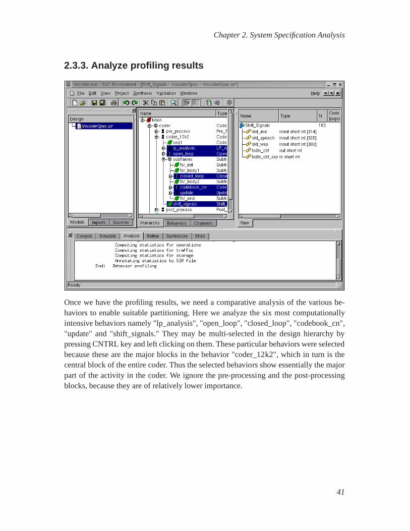
Once we have the profiling results, we need a comparative analysis of the various be-haviors to enable suitable partitioning. Here we analyze the six most computationallyintensive behaviors namely "lp_analysis", "open_loop", "closed_loop", "codebook_cn","update" and "shift_signals." They may be multi-selected in the design hierarchy bypressing CNTRL key and left clicking on them. These particular behaviors were selectedbecause these are the major blocks in the behavior "coder_12k2", which in turn is thecentral block of the entire coder. Thus the selected behaviors show essentially the majorpart of the activity in the coder. We ignore the pre-processing and the post-processingblocks, because they are of relatively lower importance.
41
Chapter 2. System Specification Analysis
2.3.3.1. Analyze profiling results (cont’d)
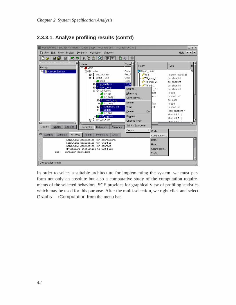
In order to select a suitable architecture for implementingthe system, we must per-form not only an absolute but also a comparative study of the computation require-ments of the selected behaviors. SCE provides for graphicalview of profiling statisticswhich may be used for this purpose. After the multi-selection, we right click and selectGraphs−→Computation from the menu bar.
42

Chapter 2. System Specification Analysis
2.3.3.2. Analyze profiling results (cont’d)
We now see a bar graph showing the relative computational intensity of the variousbehaviors in the selected behaviors. Essentially, the graph shows the number of opera-tions on the Y-axis for the individual behaviors on the X-axis. Double click on the barfor codebook_cn to view the distribution of its various operations. Note that we select"codebook_cn" because it is the behavior with the most computational complexity.
Note that the bars representing the computation for "codebook_cn" and "closed_loop"have two sections. The lower section is filled with red color and the upper section is par-tially shaded. Each speech frame consists of four sub-frames and the behaviors "code-book_cn" and "closed_loop" are executed for each subframe in contrast to other behav-iors in the graph, which are executed once. Hence the filled section of the bar representscomputation for each execution of behavior and the completebar (including the shadedsection) represents computation for the entire frame.
43
Chapter 2. System Specification Analysis
2.3.3.3. Analyze profiling results (cont’d)
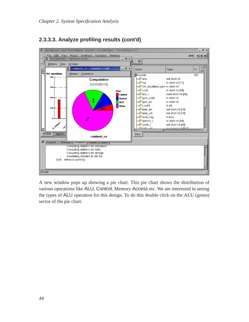
A new window pops up showing a pie chart. This pie chart shows the distribution ofvarious operations likeALU, Control, MemoryAccess etc. We are interested in seeingthe types ofALU operation for this design. To do this double click on the ALU (green)sector of the pie chart.
44
Chapter 2. System Specification Analysis
2.3.3.4. Analyze profiling results (cont’d)
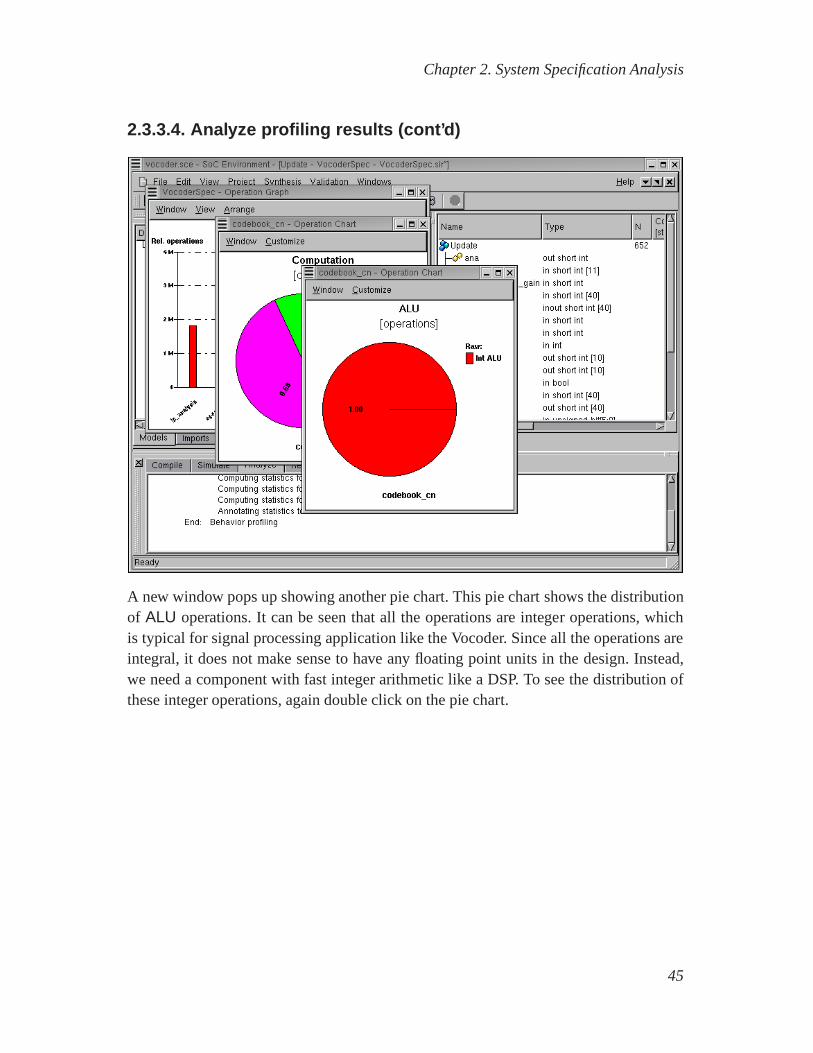
A new window pops up showing another pie chart. This pie chartshows the distributionof ALU operations. It can be seen that all the operations are integer operations, whichis typical for signal processing application like the Vocoder. Since all the operations areintegral, it does not make sense to have any floating point units in the design. Instead,we need a component with fast integer arithmetic like a DSP. To see the distribution ofthese integer operations, again double click on the pie chart.
45
Chapter 2. System Specification Analysis
2.3.3.5. Analyze profiling results (cont’d)
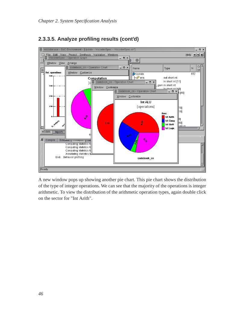
A new window pops up showing another pie chart. This pie chartshows the distributionof the type of integer operations. We can see that the majority of the operations is integerarithmetic. To view the distribution of the arithmetic operation types, again double clickon the sector for "Int Arith".
46
Chapter 2. System Specification Analysis
2.3.3.6. Analyze profiling results (cont’d)
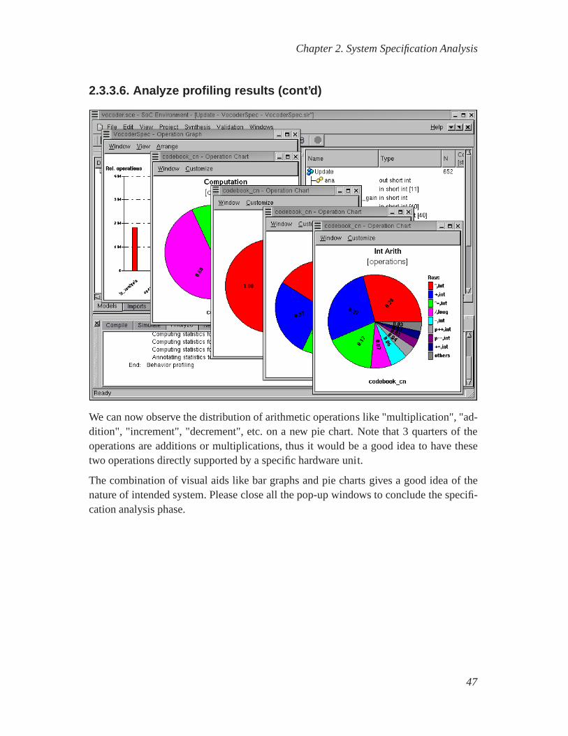
We can now observe the distribution of arithmetic operations like "multiplication", "ad-dition", "increment", "decrement", etc. on a new pie chart.Note that 3 quarters of theoperations are additions or multiplications, thus it wouldbe a good idea to have thesetwo operations directly supported by a specific hardware unit.
The combination of visual aids like bar graphs and pie chartsgives a good idea of thenature of intended system. Please close all the pop-up windows to conclude the specifi-cation analysis phase.
47

Chapter 2. System Specification Analysis
2.4. SummaryIn this chapter we looked at how to start with the system specification and analyze itscharacteristics. We were familiarized with the SCE graphical user interface and the pro-filing, analysis and simulation tools. By means of graphicaltools, we were able to tra-verse the hierarchy of the system specification model. Graphical representations alsoprovided us with information on connectivity between behaviors in the design. The userfriendliness of these representations allows us to analyzeour design better which wouldotherwise be very cumbersome.
Profiling and statistical data about the specification modelalso gives us interesting hints.For instance, the nature of computation in the model shows usthe appropriate compo-nents to consider for the system architecture. Similarly, pie charts and bar graphs for thedistribution of computation show us the critical behaviorsand their nature. As we moveforward in the system design process, we will have to make design decisions at variousstages and such statistical analysis will be of great value.In future implementations onthe tool, these analysis results may even be fed to automatictools to generate optimalsystem architectures.
48

Chapter 3. System Level Design
3.1. Overview
Figure 3-1. System level design phase using SCE
System design is increasingly being performed at higher levels of abstraction to dealwith a variety of issues. In this chapter, we look at system level design tasks with SCEas highlighted inFigure 3-1. Firstly, we need to deal with both HW and SW in a sin-gle model. Secondly, and more importantly, complexity becomes unmanageable. In thischapter we will look at the system level design phase as shownin the above figure. Thisphase comprises of architecture exploration, serialization/RTOS insertion and commu-nication synthesis. Architecture exploration deals with coming up with a suitable systemarchitecture and distributing the system tasks in the specification onto those components.Since each component has a single control, we need to serialize the tasks in each com-ponent. Tasks that are mapped to SW can be dynamically scheduled on the processorby inserting an RTOS model. Finally, we perform communication synthesis to come upwith a communication architecture and refine the data transfer and interfaces to use the
49

Chapter 3. System Level Design
communication architecture. The goal of this phase is to come up with a model that canserve as an input to RTL synthesis for HW components and SW generation for proces-sors.
50
Chapter 3. System Level Design
3.2. Architecture ExplorationArchitecture exploration is the design step to find the system level architecture and mapdifferent parts of the specification to the allocated systemcomponents under design con-straints. It consists of the tasks of selecting the target set of components, mapping behav-iors to the selected components and implementing correct synchronization between thecomponents. Note that the components themselves are independent entities that executein a parallel composition. In order to maintain the originalsemantics of the specifica-tion, the components need to be synchronized as necessary. Architecture exploration isusually an iterative process, where different candidate architectures and mappings areexperimented to search for a satisfactory solution.
As indicated earlier, the timing constraint for the Vocoderdesign is the real time re-sponse requirement, i.e., the time to encode and decode the speech should be less thanthe speech time. The test speech has a 3.26 seconds duration.Therefore, the final im-plementation must meet this time constraint. In this chapter we see how we arrive ata suitable architecture with keeping this requirement in mind and using the refinementtool.
51

Chapter 3. System Level Design
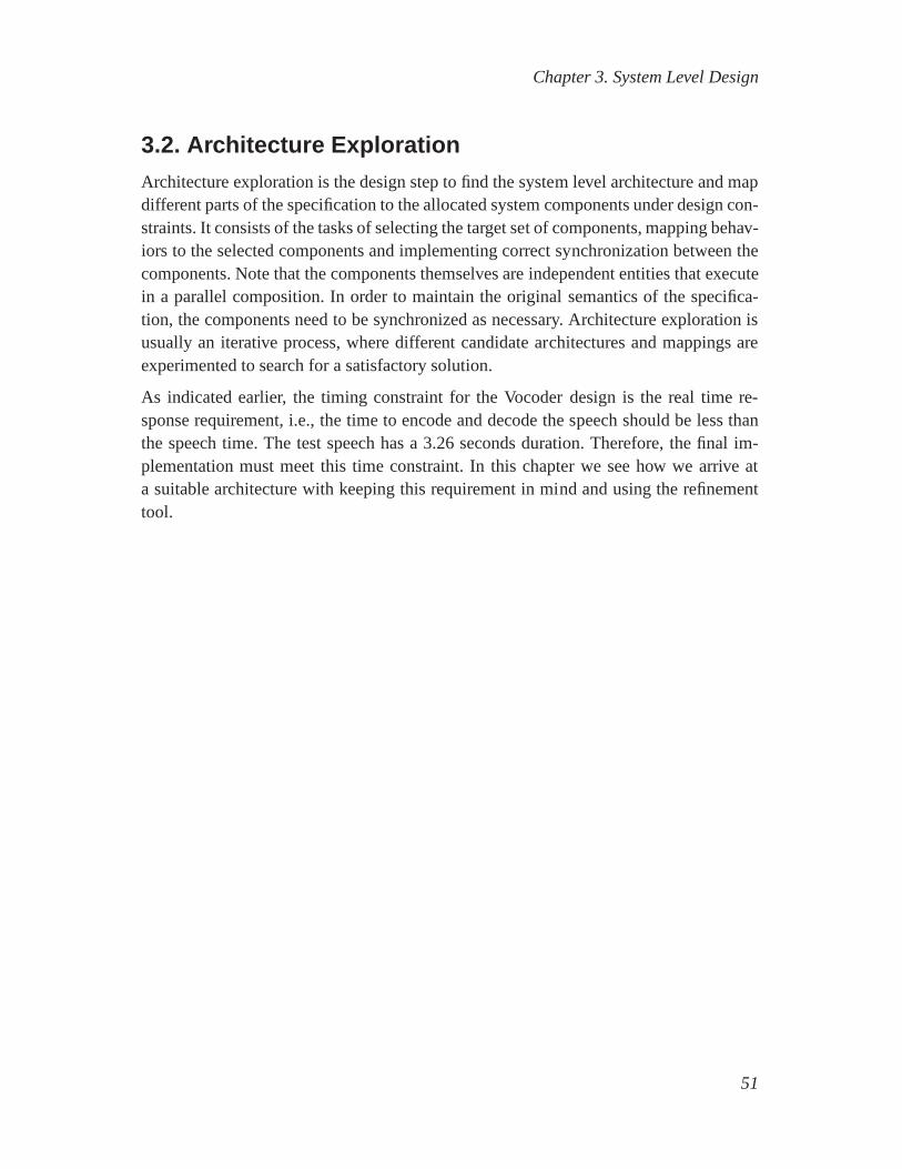
3.2.1. Try pure software implementation
The goal of our exploration process is to implement the givenfunctionality on a minimalcost architecture and still meet the timing constraint. Thefirst approach is to implementeverything in software so that we do not have the overhead of adding extra hardware andassociated interfaces. To accomplish this, we first select aprocessor out of our compo-nent database. Thereafter, we map the entire specification on to this processor. Once themapping is done, we invoke the analysis tool to see if the processor alone is sufficient toimplement the system.
52
Chapter 3. System Level Design
3.2.1.1. Try pure software implementation (cont’d)
Before we move on, the top level behavior of the design needs to be specified. This isnecessary because the specification model may have some testbench behaviors, whichare not going to be included in the final design. It may be recalled that the project weare working with involves not only the design-under-test (DUT) but also the behaviorsthat drive it. For example, the behaviors "Monitor" and "Stimilus" are just testbenchbehaviors while the behavior "Coder" represents the real design. To specify "Coder" asthe top level behavior, right click on "Coder" to bring up a drop box menu then left clickon Set As Top-Level.
53
Chapter 3. System Level Design
3.2.1.2. Try pure software implementation (cont’d)
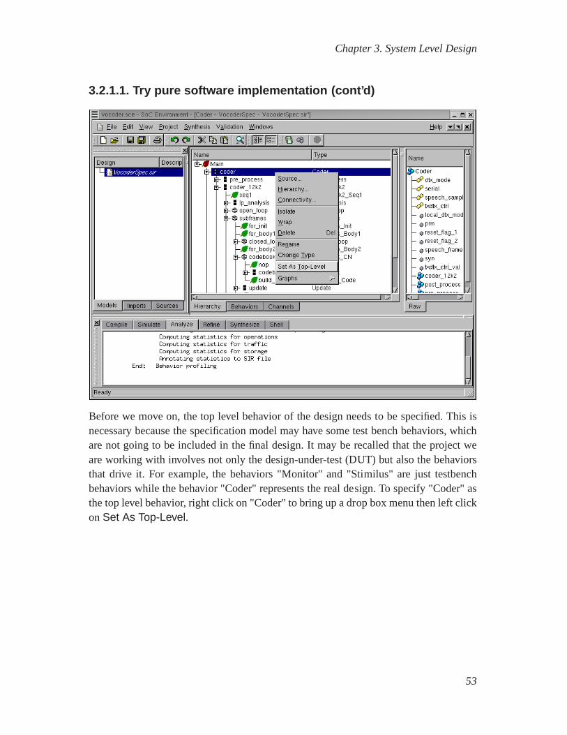
As shown in the figure, when the top level behavior "Coder" is specified, the names ofall its child behaviors are italicized to distinguish them from the test bench behaviors. Ingeneral, any behavior which needs to be tested can be set as top level. So, in a genericsense, the design under test can be identified by the italicized font.
54

Chapter 3. System Level Design
3.2.1.3. Try pure software implementation (cont’d)
We begin by exploring the available set of components in the database. This is requiredto select a suitable processor. To view all available components and select the desiredprocessor, selectSynthesis−→Allocate PEs... from the menu bar.
55
Chapter 3. System Level Design
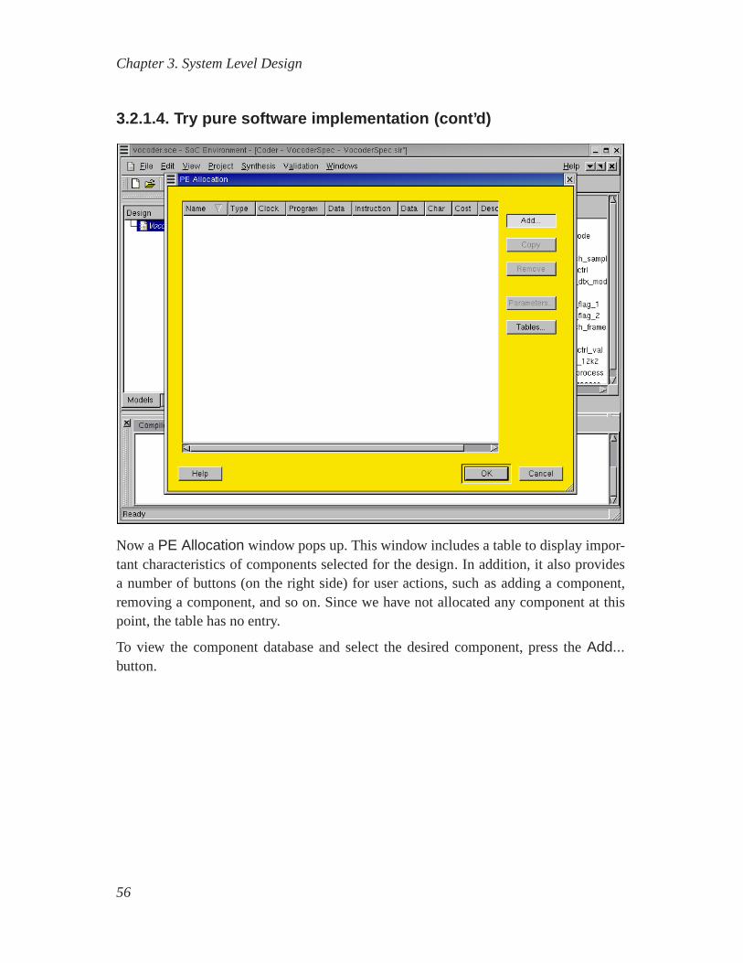
3.2.1.4. Try pure software implementation (cont’d)
Now aPE Allocation window pops up. This window includes a table to display impor-tant characteristics of components selected for the design. In addition, it also providesa number of buttons (on the right side) for user actions, suchas adding a component,removing a component, and so on. Since we have not allocated any component at thispoint, the table has no entry.
To view the component database and select the desired component, press theAdd...button.
56
Chapter 3. System Level Design
3.2.1.5. Try pure software implementation (cont’d)
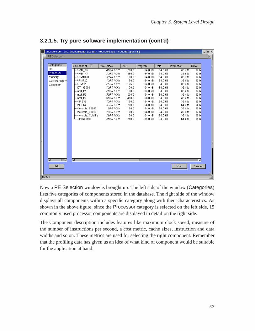
Now aPE Selection window is brought up. The left side of the window (Categories)lists five categories of components stored in the database. The right side of the windowdisplays all components within a specific category along with their characteristics. Asshown in the above figure, since theProcessor category is selected on the left side, 15commonly used processor components are displayed in detailon the right side.
The Component description includes features like maximum clock speed, measure ofthe number of instructions per second, a cost metric, cache sizes, instruction and datawidths and so on. These metrics are used for selecting the right component. Rememberthat the profiling data has given us an idea of what kind of component would be suitablefor the application at hand.
57
Chapter 3. System Level Design
3.2.1.6. Try pure software implementation (cont’d)
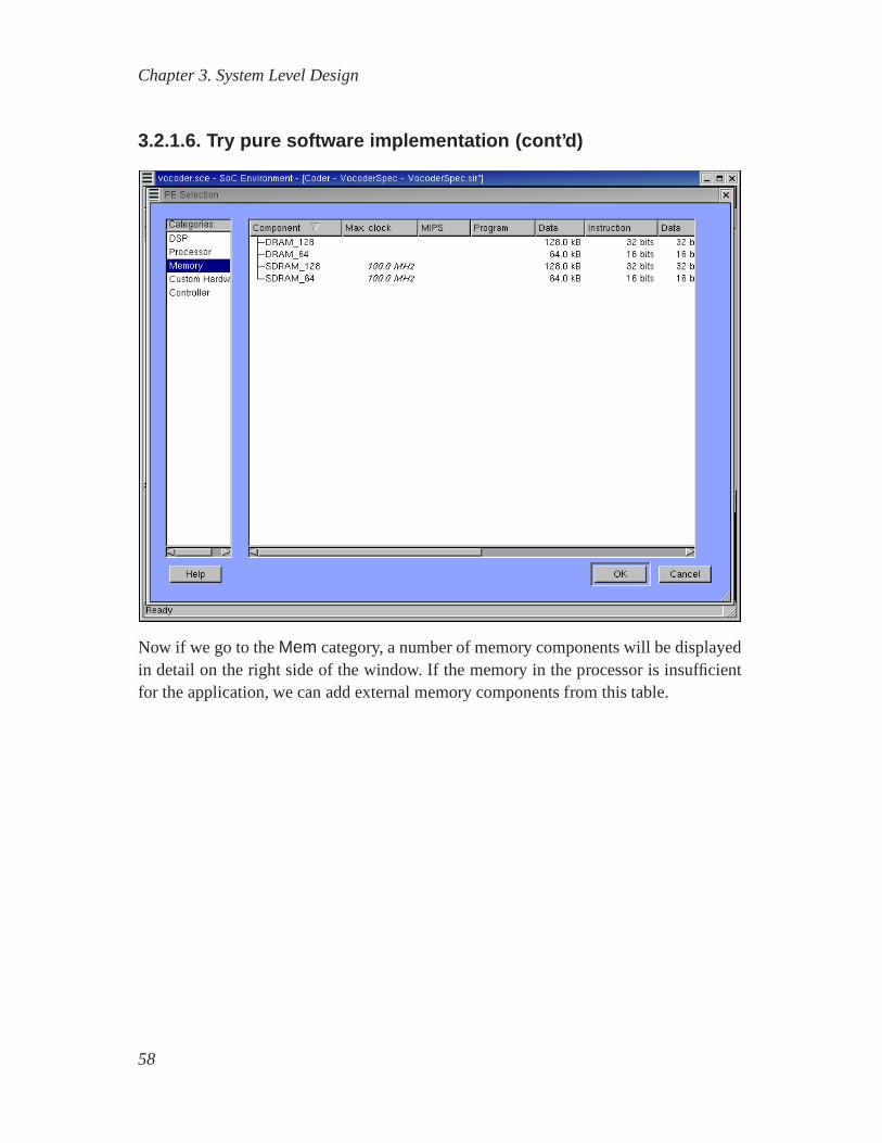
Now if we go to theMem category, a number of memory components will be displayedin detail on the right side of the window. If the memory in the processor is insufficientfor the application, we can add external memory components from this table.
58
Chapter 3. System Level Design
3.2.1.7. Try pure software implementation (cont’d)
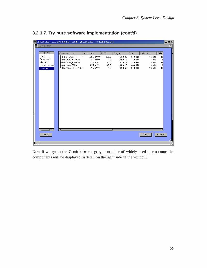
Now if we go to theController category, a number of widely used micro-controllercomponents will be displayed in detail on the right side of the window.
59

Chapter 3. System Level Design
3.2.1.8. Try pure software implementation (cont’d)
Through earlier profiling and analyzing, we found out that integer multiplication is themost significant operations in the original specification. Therefore, a fixed-point DSPwould be desirable for this design.
Under theDSP category, a number of commercially available DSPs are displayed. TheseDSP components are maintained as part of the component library and may be importedinto the design upon requirement. Since the Vocoder design project was supported byMotorola, our first choice is DSP56600 from Motorola.
Left click the "Motorola_DSP56600" row to select it. Then click OK button to confirmthe selection.
60

Chapter 3. System Level Design
3.2.1.9. Try pure software implementation (cont’d)
After clicking OK to confirm the selection in the PE Selection dialog, a new dialogwill pop up to allow entering parameters of the allocated Motorola DSP. Use the defaultparameters, i.e., accept the dialog by clickingOK.
61
Chapter 3. System Level Design
3.2.1.10. Try pure software implementation (cont’d)
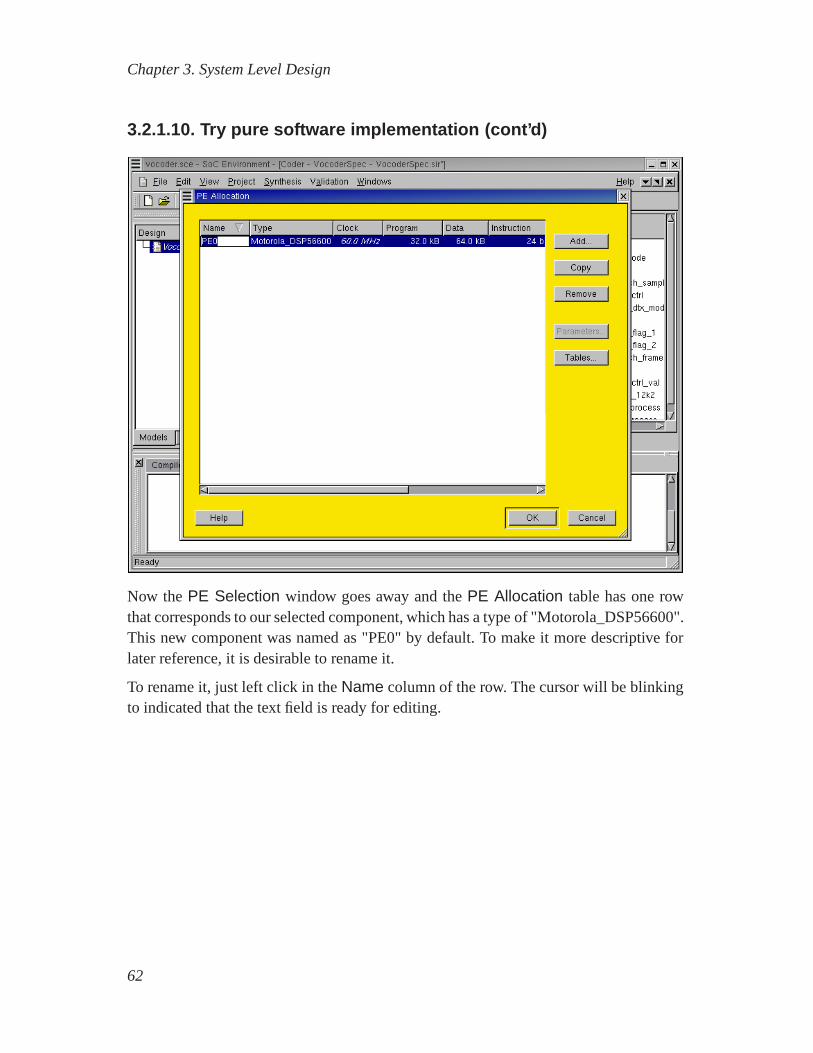
Now thePE Selection window goes away and thePE Allocation table has one rowthat corresponds to our selected component, which has a typeof "Motorola_DSP56600".This new component was named as "PE0" by default. To make it more descriptive forlater reference, it is desirable to rename it.
To rename it, just left click in theName column of the row. The cursor will be blinkingto indicated that the text field is ready for editing.
62
Chapter 3. System Level Design
3.2.1.11. Try pure software implementation (cont’d)
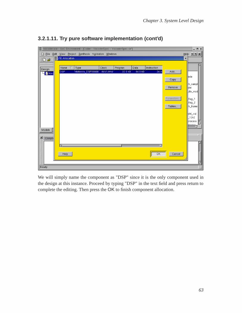
We will simply name the component as "DSP" since it is the onlycomponent used inthe design at this instance. Proceed by typing "DSP" in the text field and press return tocomplete the editing. Then press theOK to finish component allocation.
63

Chapter 3. System Level Design
3.2.1.12. Try pure software implementation (cont’d)
As mentioned earlier, we will map the whole design to the selected processor. This isdone by assign the top level behavior "Coder" to "DSP". Left click in thePE column inthe row for the "Coder" behavior. A drop box containing allocated components comesup. Left click on "DSP" to map behavior "Coder" to "DSP".
It should be noted that any kind of mapping is allowed. However, since we are inves-tigating a purely software implementation, everything in the design gets mapped to the"DSP".
64
Chapter 3. System Level Design
3.2.1.13. Try pure software implementation (cont’d)
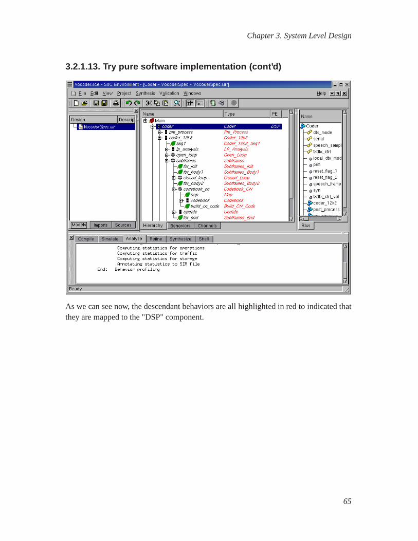
As we can see now, the descendant behaviors are all highlighted in red to indicated thatthey are mapped to the "DSP" component.
65
Chapter 3. System Level Design
3.2.2. Estimate performance
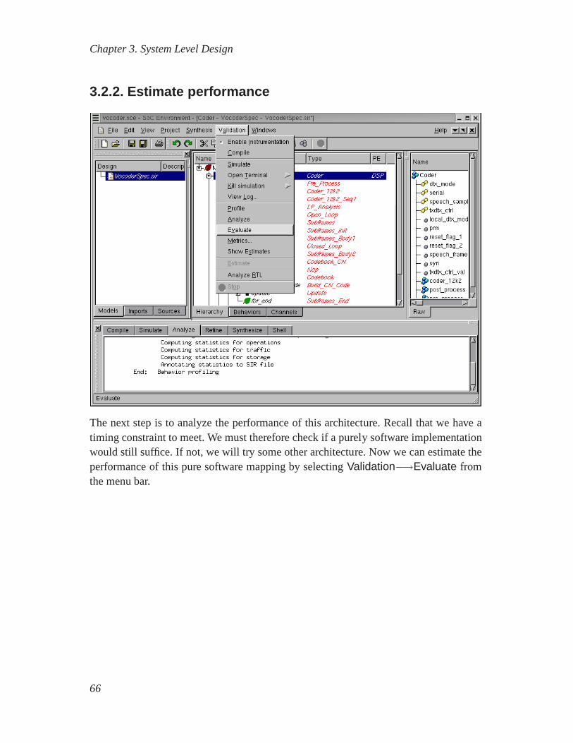
The next step is to analyze the performance of this architecture. Recall that we have atiming constraint to meet. We must therefore check if a purely software implementationwould still suffice. If not, we will try some other architecture. Now we can estimate theperformance of this pure software mapping by selectingValidation−→Evaluate fromthe menu bar.
66
Chapter 3. System Level Design
3.2.2.1. Estimate performance (cont’d)
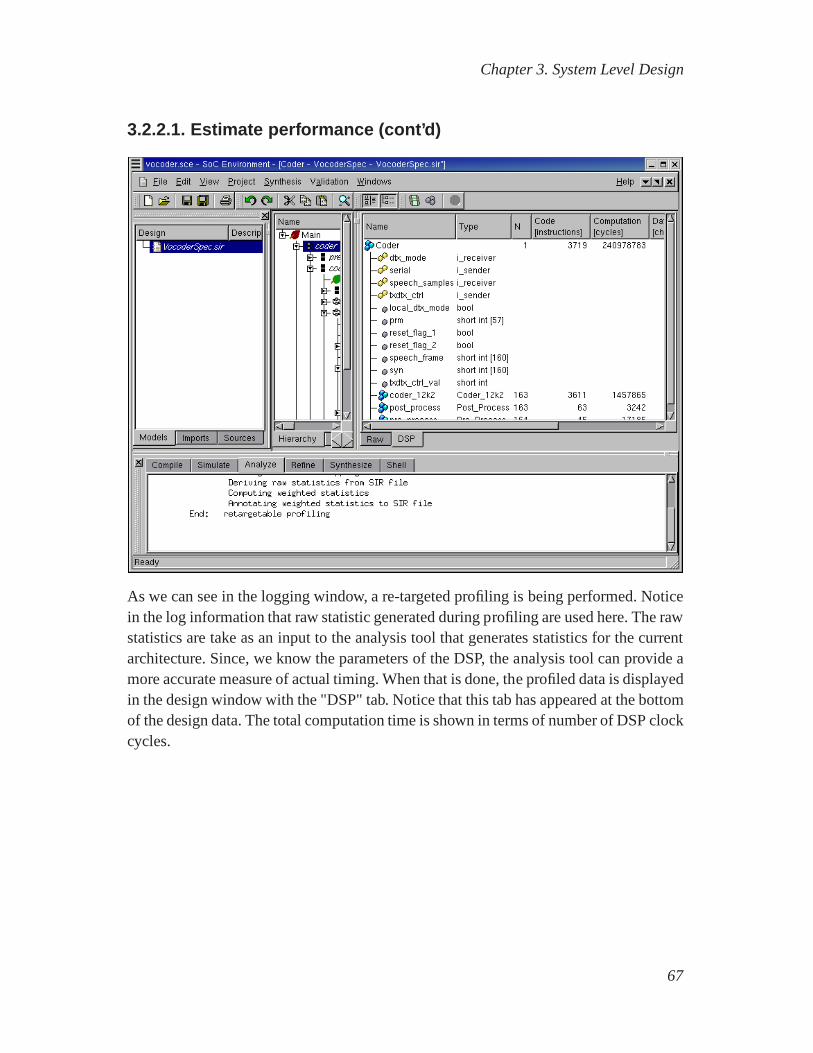
As we can see in the logging window, a re-targeted profiling isbeing performed. Noticein the log information that raw statistic generated during profiling are used here. The rawstatistics are take as an input to the analysis tool that generates statistics for the currentarchitecture. Since, we know the parameters of the DSP, the analysis tool can provide amore accurate measure of actual timing. When that is done, the profiled data is displayedin the design window with the "DSP" tab. Notice that this tab has appeared at the bottomof the design data. The total computation time is shown in terms of number of DSP clockcycles.
67

Chapter 3. System Level Design
3.2.2.2. Estimate performance (cont’d)
The number of computation cycles is a relevant metric for observation. However, it mustbe converted to an absolute measure of time so that we may directly verify if this archi-tecture meets the demands. To find out the real execution timein terms of seconds, weturn on the option for estimation by selectingValidation−→Show Estimates from themenu bar.
68
Chapter 3. System Level Design
3.2.2.3. Estimate performance (cont’d)
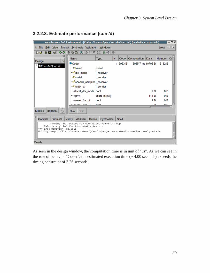
As seen in the design window, the computation time is in unit of "us". As we can see inthe row of behavior "Coder", the estimated execution time (~4.00 seconds) exceeds thetiming constraint of 3.26 seconds.
69
Chapter 3. System Level Design
3.2.2.4. Estimate performance (cont’d)
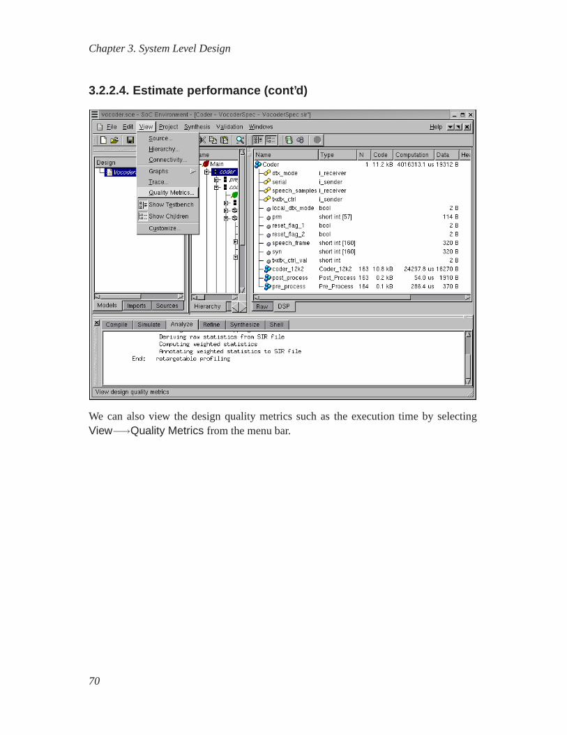
We can also view the design quality metrics such as the execution time by selectingView−→Quality Metrics from the menu bar.
70
Chapter 3. System Level Design
3.2.2.5. Estimate performance (cont’d)
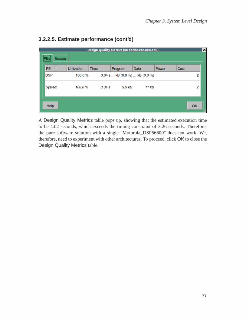
A Design Quality Metrics table pops up, showing that the estimated execution timeto be 4.02 seconds, which exceeds the timing constraint of 3.26 seconds. Therefore,the pure software solution with a single "Motorola_DSP56600" does not work. We,therefore, need to experiment with other architectures. Toproceed, clickOK to close theDesign Quality Metrics table.
71

Chapter 3. System Level Design
3.2.3. Try software/hardware implementation
From what we observed while studying the vocoder specification, the design is mostlysequential. There is not much parallelism to exploit. What we need to reduce the execu-tion time is a much faster component than the DSP we used. Someof the critical timeconsuming tasks may be mapped to a fast hardware. In this iteration, we will try to addone hardware component along with the DSP to implement the design. As we found outearlier, one of the computationally intensive and criticalpart in the Vocoder is the Code-book behavior. We hope to speed it up by mapping it to a custom hardware componentand execute the remaining behaviors on the DSP.
72
Chapter 3. System Level Design
3.2.3.1. Try software/hardware implementation (cont’d)
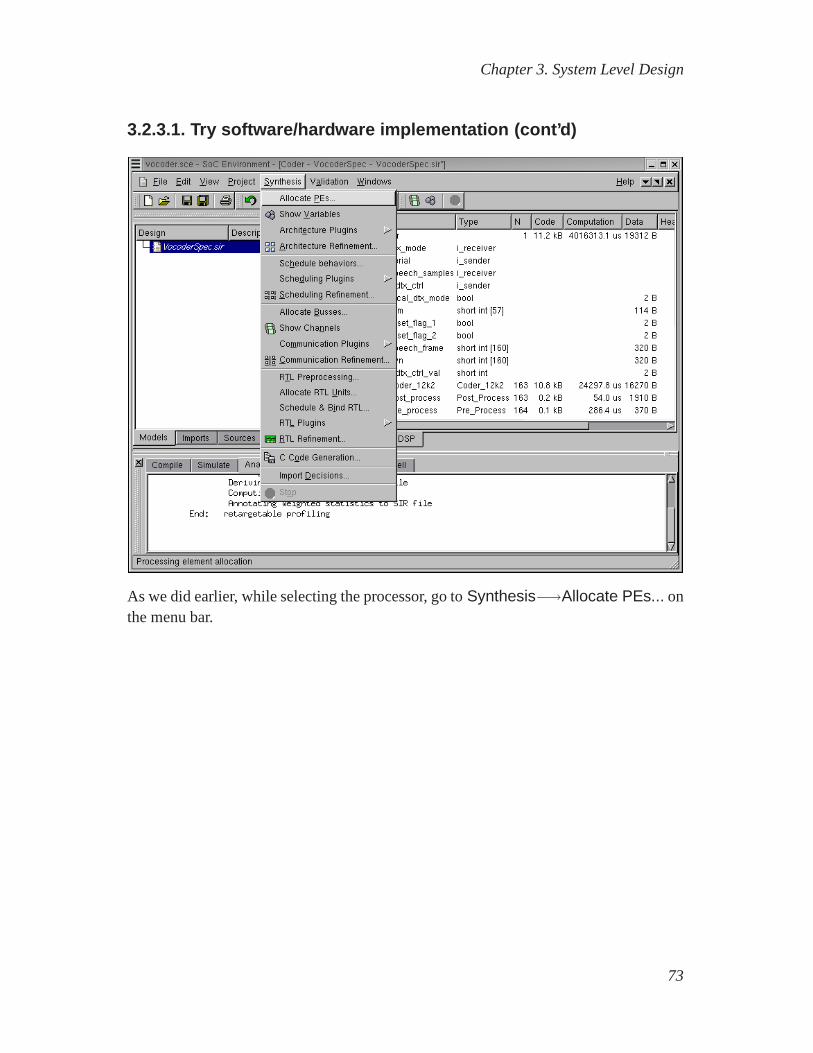
As we did earlier, while selecting the processor, go toSynthesis−→Allocate PEs... onthe menu bar.
73
Chapter 3. System Level Design
3.2.3.2. Try software/hardware implementation (cont’d)
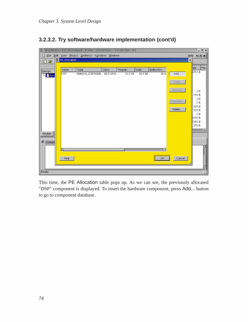
This time, thePE Allocation table pops up. As we can see, the previously allocated"DSP" component is displayed. To insert the hardware component, pressAdd... buttonto go to component database.
74
Chapter 3. System Level Design
3.2.3.3. Try software/hardware implementation (cont’d)
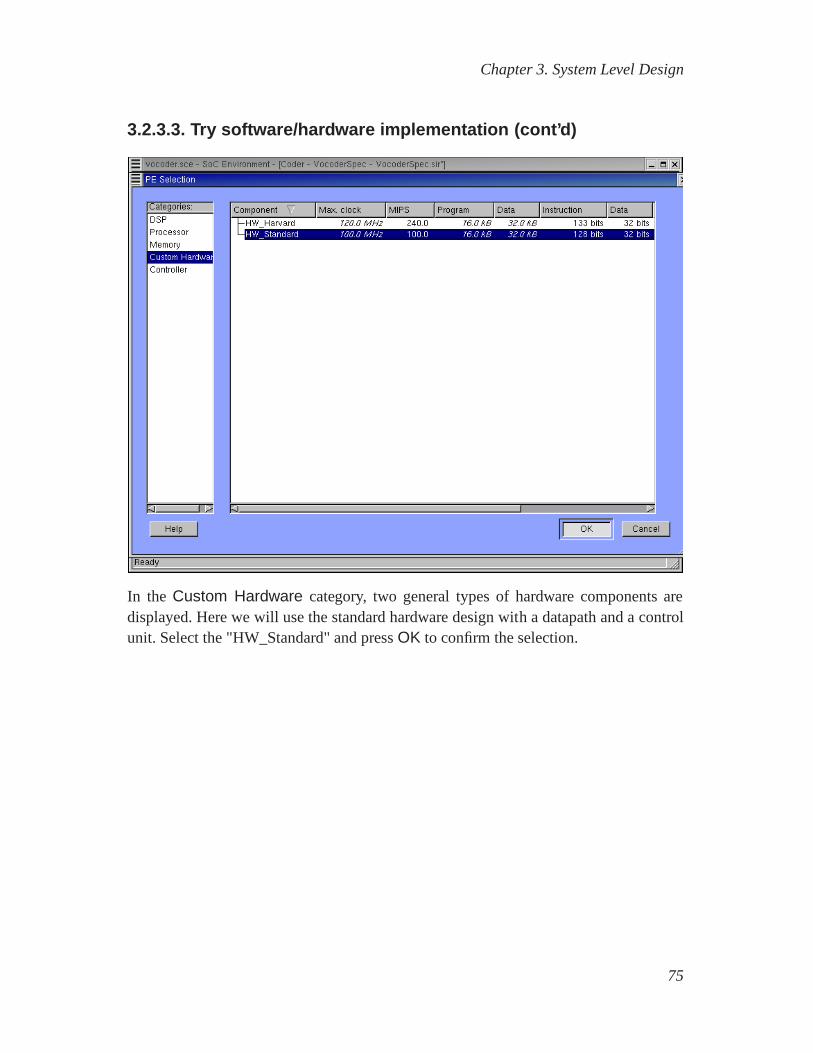
In the Custom Hardware category, two general types of hardware components aredisplayed. Here we will use the standard hardware design with a datapath and a controlunit. Select the "HW_Standard" and pressOK to confirm the selection.
75

Chapter 3. System Level Design
3.2.3.4. Try software/hardware implementation (cont’d)
Now the "HW_Standard" component is added to thePE Allocation table. In the sameway we did for the "DSP" component, we simply rename it to "HW"to distinguish it.Notice that for the hardware component, some metrics are flexible. For instance, theclock period may be changed. However, we stay with the current speed of 100 Mhz fordemo purpose.
76
Chapter 3. System Level Design
3.2.3.5. Try software/hardware implementation (cont’d)
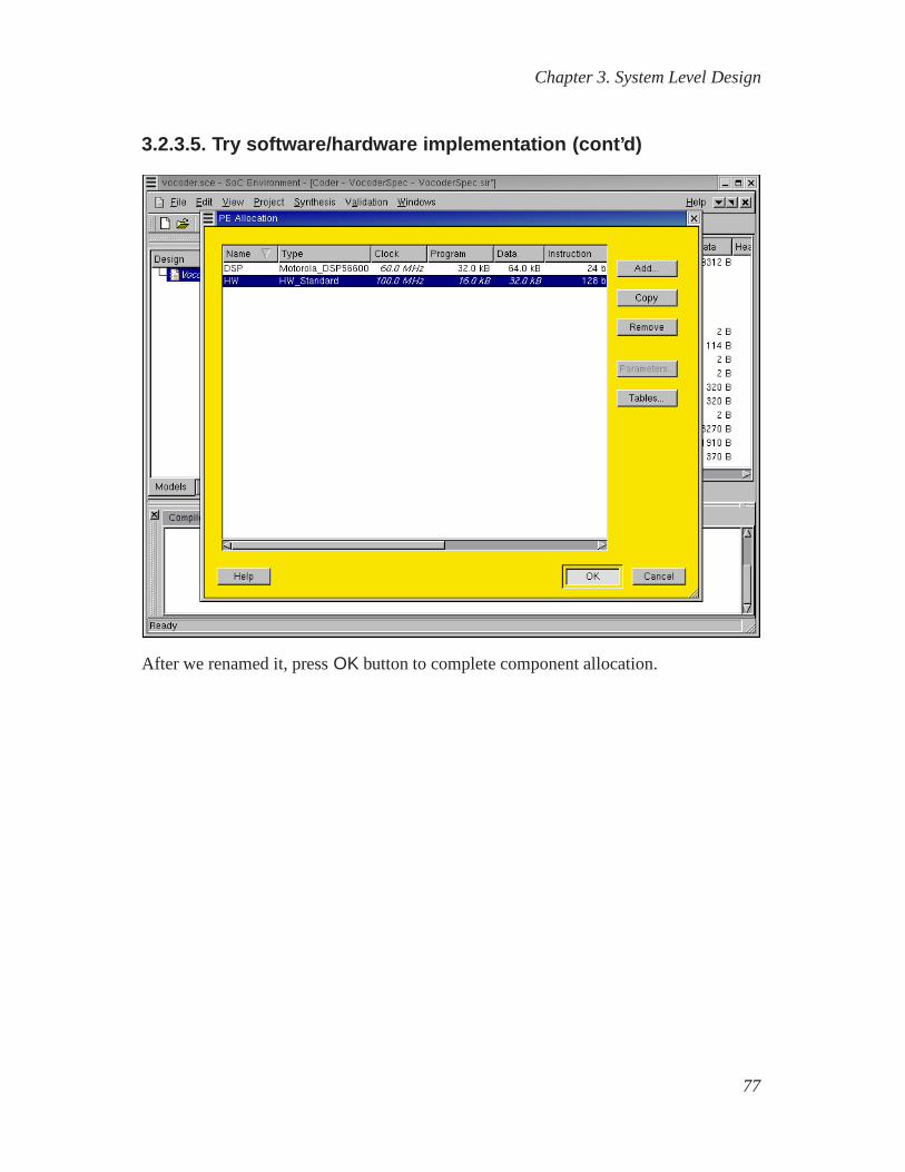
After we renamed it, pressOK button to complete component allocation.
77
Chapter 3. System Level Design
3.2.3.6. Try software/hardware implementation (cont’d)
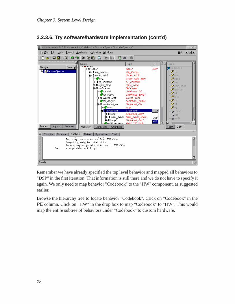
Remember we have already specified the top level behavior andmapped all behaviors to"DSP" in the first iteration. That information is still thereand we do not have to specify itagain. We only need to map behavior "Codebook" to the "HW" component, as suggestedearlier.
Browse the hierarchy tree to locate behavior "Codebook". Click on "Codebook" in thePE column. Click on "HW" in the drop box to map "Codebook" to "HW". This wouldmap the entire subtree of behaviors under "Codebook" to custom hardware.
78
Chapter 3. System Level Design
3.2.3.7. Try software/hardware implementation (cont’d)
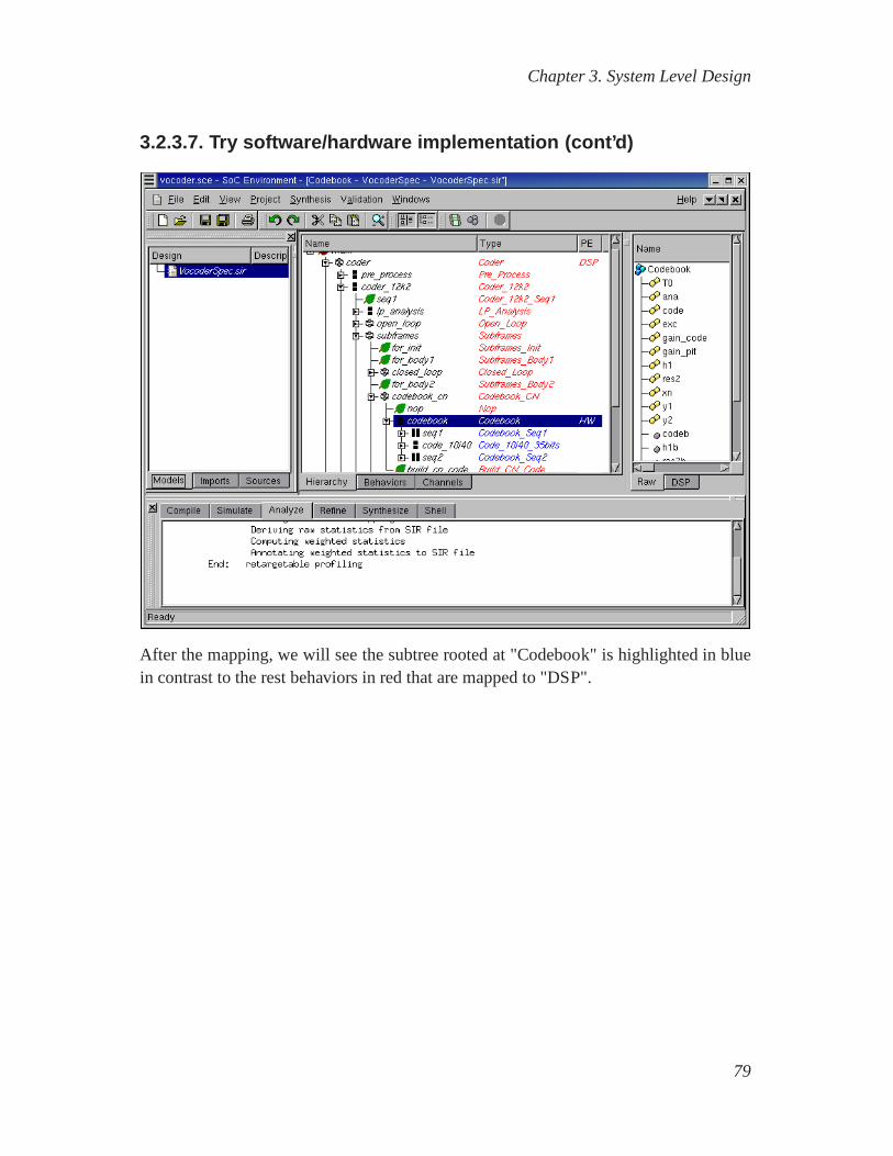
After the mapping, we will see the subtree rooted at "Codebook" is highlighted in bluein contrast to the rest behaviors in red that are mapped to "DSP".
79
Chapter 3. System Level Design
3.2.4. Estimate performance
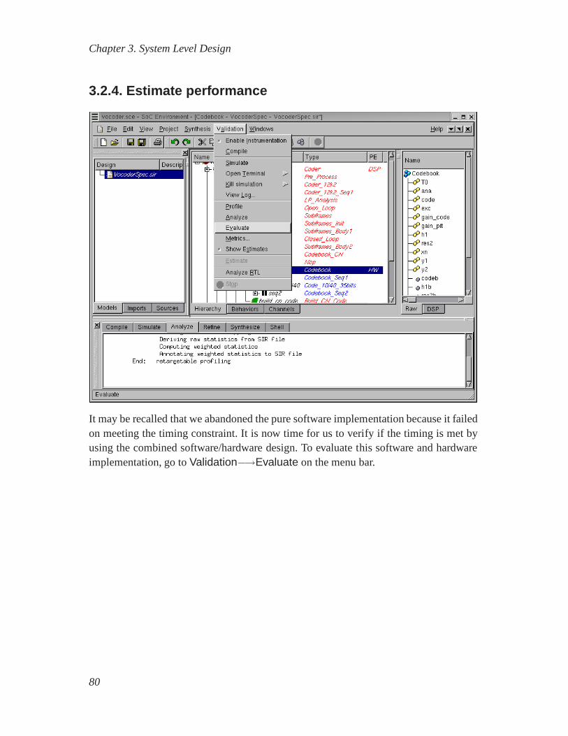
It may be recalled that we abandoned the pure software implementation because it failedon meeting the timing constraint. It is now time for us to verify if the timing is met byusing the combined software/hardware design. To evaluate this software and hardwareimplementation, go toValidation−→Evaluate on the menu bar.
80
Chapter 3. System Level Design
3.2.4.1. Estimate performance (cont’d)
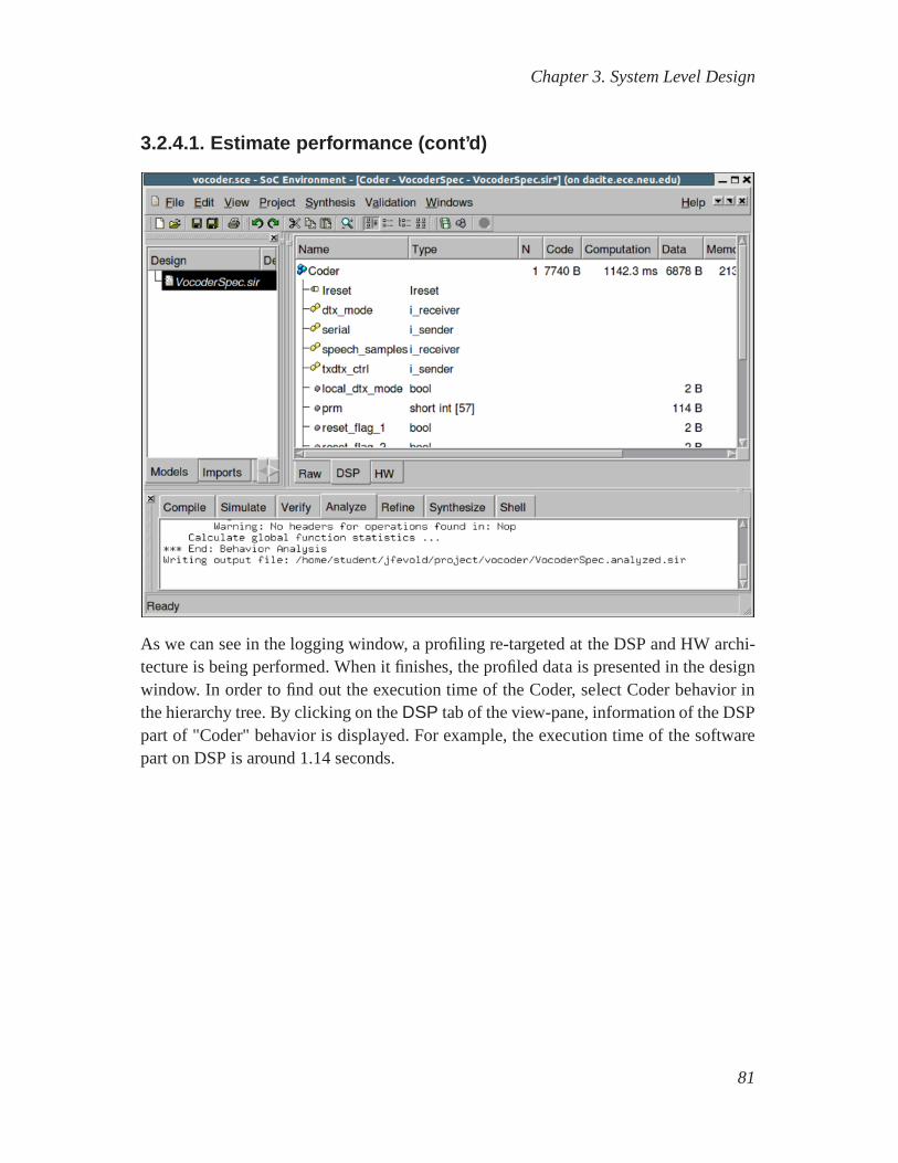
As we can see in the logging window, a profiling re-targeted atthe DSP and HW archi-tecture is being performed. When it finishes, the profiled data is presented in the designwindow. In order to find out the execution time of the Coder, select Coder behavior inthe hierarchy tree. By clicking on theDSP tab of the view-pane, information of the DSPpart of "Coder" behavior is displayed. For example, the execution time of the softwarepart on DSP is around 1.14 seconds.
81
Chapter 3. System Level Design
3.2.4.2. Estimate performance (cont’d)
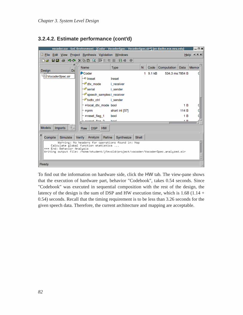
To find out the information on hardware side, click theHW tab. The view-pane showsthat the execution of hardware part, behavior "Codebook", takes 0.54 seconds. Since"Codebook" was executed in sequential composition with therest of the design, thelatency of the design is the sum of DSP and HW execution time, which is 1.68 (1.14 +0.54) seconds. Recall that the timing requirement is to be less than 3.26 seconds for thegiven speech data. Therefore, the current architecture andmapping are acceptable.
82
Chapter 3. System Level Design
3.2.4.3. Estimate performance (cont’d)
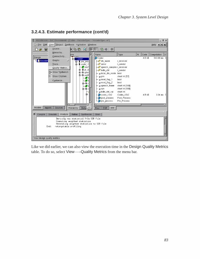
Like we did earlier, we can also view the execution time in theDesign Quality Metricstable. To do so, selectView−→Quality Metrics from the menu bar.
83

Chapter 3. System Level Design
3.2.4.4. Estimate performance (cont’d)
As shown in the figure, theDesign Quality Metrics table including a number of designquality metrics is displayed. It confirms that the total execution time is 1.68 seconds,same as what we figured out earlier. After reviewing the quality metrics, click onOK toclose the table.
84

Chapter 3. System Level Design
3.2.5. Generate architecture model
Now we can refine the specification model into an architecturemodel, which will exactlyreflect the this architecture and mapping decisions. This can be done either manually orautomatically. As we mentioned earlier, an architecture refinement tool is integratedin SCE. To invoke the tool, go toSynthesis−→Architecture Refinement.... The toolchanges the model to reflect the partition we created and alsointroduces synchronizationbetween the parallely executing components. Note that we have not decided to mapvariables explicitly to components. For demo purposes, we will leave this decision to bemade automatically by the refinement tool. However, it needsto be mentioned that thedesigner may choose to map variables in the design as deemed suitable.
85
Chapter 3. System Level Design
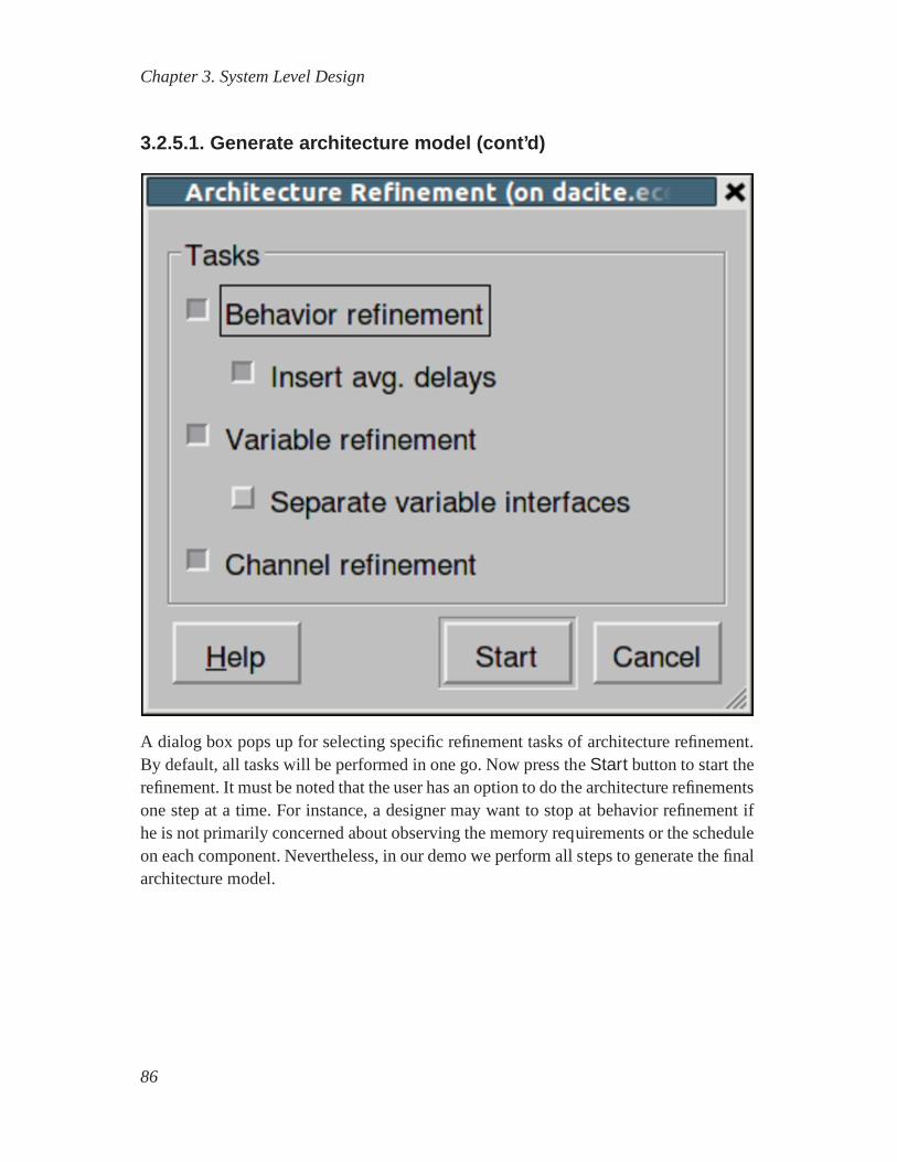
3.2.5.1. Generate architecture model (cont’d)
A dialog box pops up for selecting specific refinement tasks ofarchitecture refinement.By default, all tasks will be performed in one go. Now press theStart button to start therefinement. It must be noted that the user has an option to do the architecture refinementsone step at a time. For instance, a designer may want to stop atbehavior refinement ifhe is not primarily concerned about observing the memory requirements or the scheduleon each component. Nevertheless, in our demo we perform all steps to generate the finalarchitecture model.
86
Chapter 3. System Level Design
3.2.5.2. Generate architecture model (cont’d)
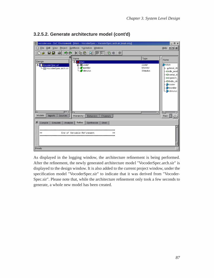
As displayed in the logging window, the architecture refinement is being performed.After the refinement, the newly generated architecture model "VocoderSpec.arch.sir" isdisplayed to the design window. It is also added to the current project window, under thespecification model "VocoderSpec.sir" to indicate that it was derived from "Vocoder-Spec.sir". Please note that, while the architecture refinement only took a few seconds togenerate, a whole new model has been created.
87
Chapter 3. System Level Design
3.2.6. Browse architecture model
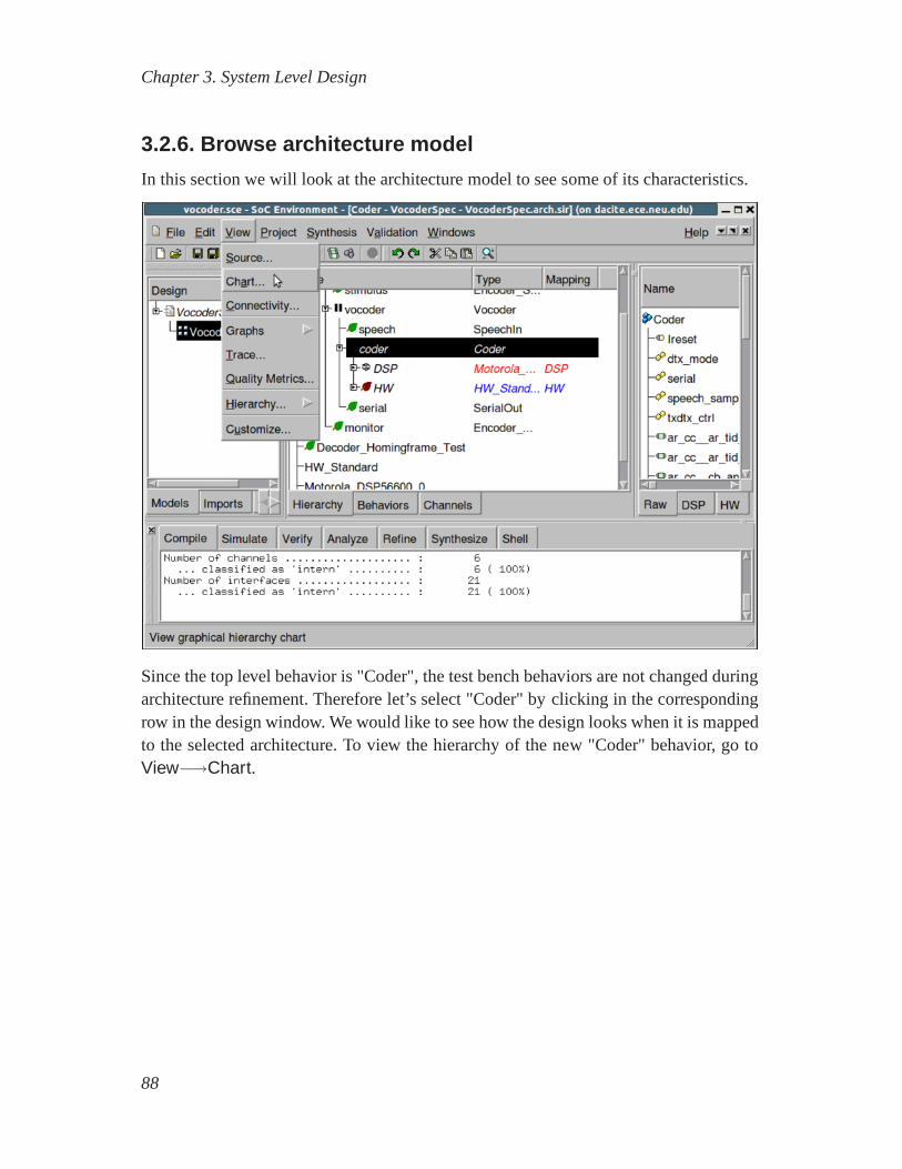
In this section we will look at the architecture model to see some of its characteristics.
Since the top level behavior is "Coder", the test bench behaviors are not changed duringarchitecture refinement. Therefore let’s select "Coder" byclicking in the correspondingrow in the design window. We would like to see how the design looks when it is mappedto the selected architecture. To view the hierarchy of the new "Coder" behavior, go toView−→Chart.
88

Chapter 3. System Level Design
3.2.6.1. Browse architecture model (cont’d)
A window pops up, showing all sub-behaviors of the "Coder" behavior. As we can see,this new top level behavior Coder in the architecture model is composed of two newbehaviors, "DSP" and "HW", which were constructed and inserted during architecturerefinement. These behaviors at the top level indicate the presence of two components se-lected in the architecture. Note that they are also composedin parallel, which representsthe actual semantics of the architecture model.
89
Chapter 3. System Level Design
3.2.6.2. Browse architecture model (cont’d)
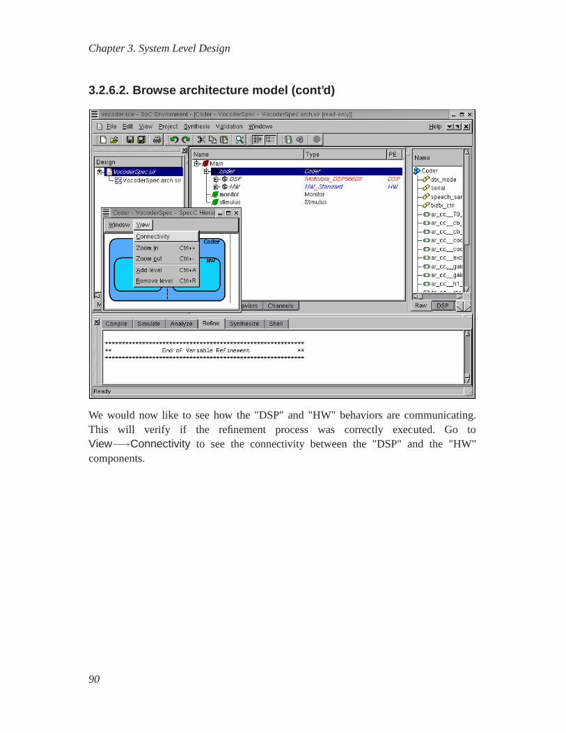
We would now like to see how the "DSP" and "HW" behaviors are communicating.This will verify if the refinement process was correctly executed. Go toView−→Connectivity to see the connectivity between the "DSP" and the "HW"components.
90
Chapter 3. System Level Design
3.2.6.3. Browse architecture model (cont’d)
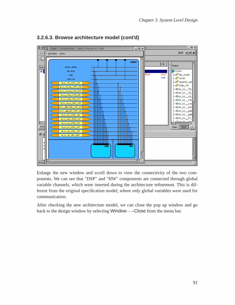
Enlarge the new window and scroll down to view the connectivity of the two com-ponents. We can see that "DSP" and "HW" components are connected through globalvariable channels, which were inserted during the architecture refinement. This is dif-ferent from the original specification model, where only global variables were used forcommunication.
After checking the new architecture model, we can close the pop up window and goback to the design window by selectingWindow−→Close from the menu bar.
91

Chapter 3. System Level Design
3.2.6.4. Rename architecture model
Like what we did for the specification model, we also change the name of the new modelto be "VocoderArch.sir" in the project window. The renamingis just for the purpose ofmaintaining a nomenclature schema and to correctly identify the individual models.
92
Chapter 3. System Level Design
3.2.7. Simulate architecture model (optional)
This section shows the simulation of the generated architecture model. If thereader is not interested, she or he can skip this section and go directly toSection 3.3Software Scheduling and RTOS Model Insertion(page 96).
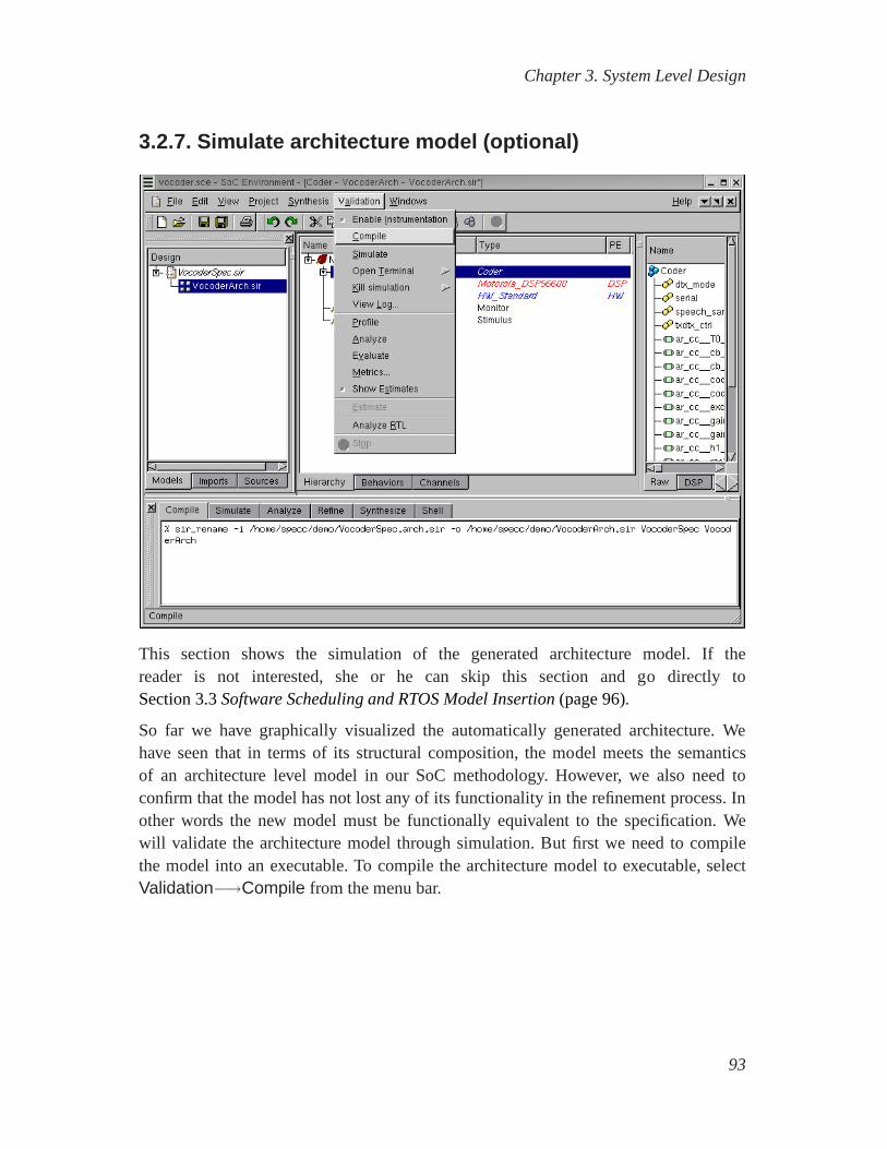
So far we have graphically visualized the automatically generated architecture. Wehave seen that in terms of its structural composition, the model meets the semanticsof an architecture level model in our SoC methodology. However, we also need toconfirm that the model has not lost any of its functionality inthe refinement process. Inother words the new model must be functionally equivalent tothe specification. Wewill validate the architecture model through simulation. But first we need to compilethe model into an executable. To compile the architecture model to executable, selectValidation−→Compile from the menu bar.
93
Chapter 3. System Level Design
3.2.7.1. Simulate architecture model (optional) (cont’d)
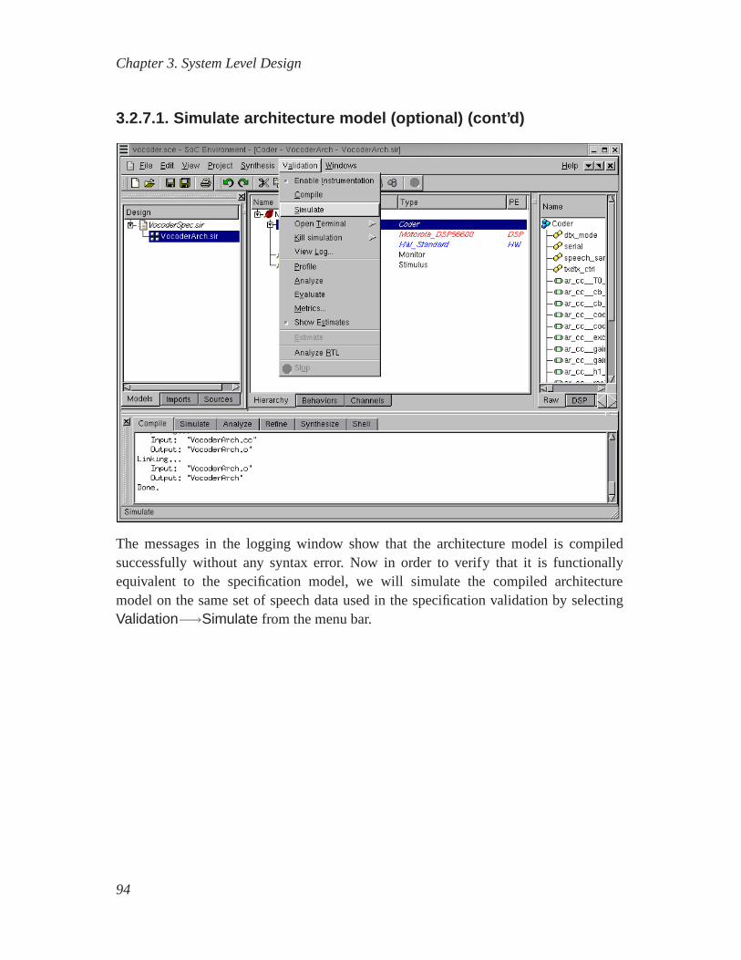
The messages in the logging window show that the architecture model is compiledsuccessfully without any syntax error. Now in order to verify that it is functionallyequivalent to the specification model, we will simulate the compiled architecturemodel on the same set of speech data used in the specification validation by selectingValidation−→Simulate from the menu bar.
94
Chapter 3. System Level Design
3.2.7.2. Simulate architecture model (optional) (cont’d)
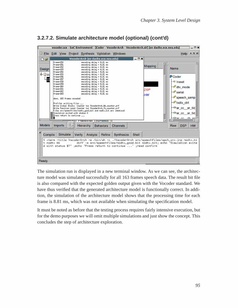
The simulation run is displayed in a new terminal window. As we can see, the architec-ture model was simulated successfully for all 163 frames speech data. The result bit fileis also compared with the expected golden output given with the Vocoder standard. Wehave thus verified that the generated architecture model is functionally correct. In addi-tion, the simulation of the architecture model shows that the processing time for eachframe is 8.81 ms, which was not available when simulating thespecification model.
It must be noted as before that the testing process requires fairly intensive execution, butfor the demo purposes we will omit multiple simulations and just show the concept. Thisconcludes the step of architecture exploration.
95
Chapter 3. System Level Design
3.3. Software Scheduling and RTOS Model InsertionThe next step in the system level design process is the serialization of behavior executionon the processing elements. Processing elements (PEs) havea single thread of controlonly. Therefore, behaviors mapped to the same PE can only execute sequentially andhave to be scheduled. Software scheduling and RTOS model insertion is the design stepto schedule the behaviors inside each PE.
Depending on the nature of the PE and the data inter-dependencies, behaviors are sched-uled statically or dynamically. In a static scheduling approach, behaviors are executed ina fixed and predetermined order, possibly flattening parts ofthe behavioral hierarchy. Ina dynamic scheduling approach on the other hand, the order ofexecution is determineddynamically during runtime. Behaviors are arranged into potentially concurrent tasks.Inside each task, behaviors are executed sequentially. A RTOS model is inserted into thedesign. The RTOS model maintains a pool of task behaviors anddynamically selectsa task to execute according to its scheduling algorithm. In this chapter we see how wemake scheduling decisions using SCE.
96

Chapter 3. System Level Design
3.3.1. Serialize behaviors
To start behavior scheduling, selectSynthesis−→Schedule behaviors from the menubar.
97
Chapter 3. System Level Design
3.3.1.1. Schedule software
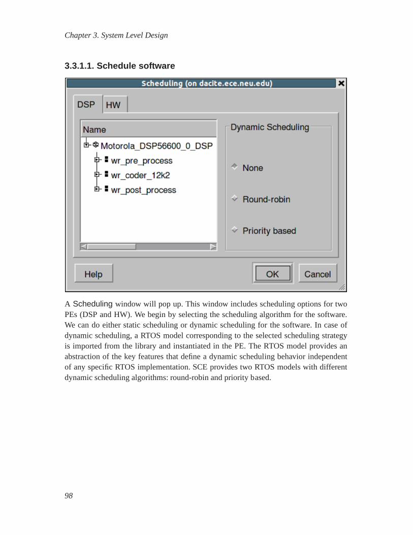
A Scheduling window will pop up. This window includes scheduling optionsfor twoPEs (DSP and HW). We begin by selecting the scheduling algorithm for the software.We can do either static scheduling or dynamic scheduling forthe software. In case ofdynamic scheduling, a RTOS model corresponding to the selected scheduling strategyis imported from the library and instantiated in the PE. The RTOS model provides anabstraction of the key features that define a dynamic scheduling behavior independentof any specific RTOS implementation. SCE provides two RTOS models with differentdynamic scheduling algorithms: round-robin and priority based.
98
Chapter 3. System Level Design
3.3.1.2. Schedule software (cont’d)
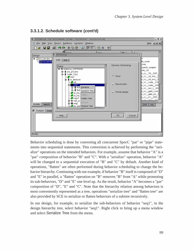
Behavior scheduling is done by converting all concurrent SpecC "par" or "pipe" state-ments into sequential statements. This conversion is achieved by performing the "seri-alize" operations on the intended behaviors. For example, assume that behavior "A" is a"par" composition of behavior "B" and "C". With a "serialize" operation, behavior "A"will be changed to a sequential execution of "B" and "C" by default. Another kind ofoperations, "flatten" are often performed during behavior scheduling to change the be-havior hierarchy. Continuing with our example, if behavior"B" itself is composed of "D"and "E" in parallel, a "flatten" operation on "B" removes "B" from "A" while promotingits sub-behaviors, "D" and "E" one level up. As the result, behavior "A" becomes a "par"composition of "D", "E" and "C". Note that the hierarchy relation among behaviors ismost conveniently represented as a tree, operations "serialize tree" and "flatten tree" arealso provided by SCE to serialize or flatten behaviors of a subtree recursively.
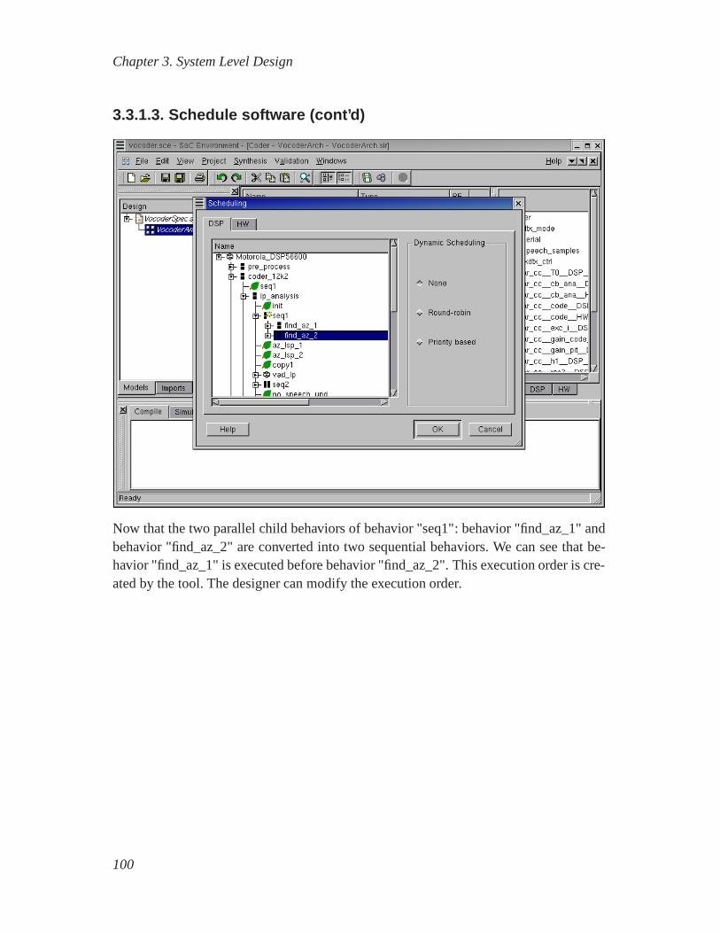
In our design, for example, to serialize the sub-behaviors of behavior "seq1", in thedesign hierarchy tree, select behavior "seq1". Right clickto bring up a menu windowand selectSerialize Tree from the menu.
99
Chapter 3. System Level Design
3.3.1.3. Schedule software (cont’d)
Now that the two parallel child behaviors of behavior "seq1": behavior "find_az_1" andbehavior "find_az_2" are converted into two sequential behaviors. We can see that be-havior "find_az_1" is executed before behavior "find_az_2".This execution order is cre-ated by the tool. The designer can modify the execution order.
100
Chapter 3. System Level Design
3.3.1.4. Schedule software (cont’d)
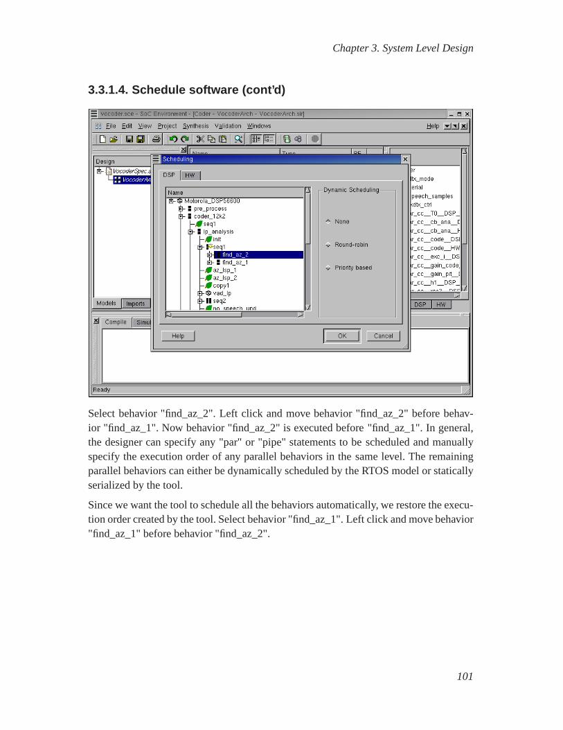
Select behavior "find_az_2". Left click and move behavior "find_az_2" before behav-ior "find_az_1". Now behavior "find_az_2" is executed before"find_az_1". In general,the designer can specify any "par" or "pipe" statements to bescheduled and manuallyspecify the execution order of any parallel behaviors in thesame level. The remainingparallel behaviors can either be dynamically scheduled by the RTOS model or staticallyserialized by the tool.
Since we want the tool to schedule all the behaviors automatically, we restore the execu-tion order created by the tool. Select behavior "find_az_1".Left click and move behavior"find_az_1" before behavior "find_az_2".
101
Chapter 3. System Level Design
3.3.1.5. Schedule software (cont’d)
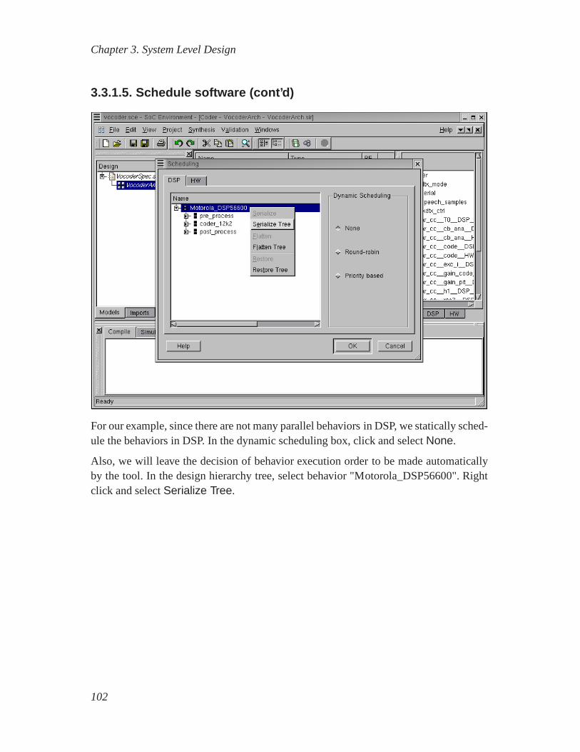
For our example, since there are not many parallel behaviorsin DSP, we statically sched-ule the behaviors in DSP. In the dynamic scheduling box, click and selectNone.
Also, we will leave the decision of behavior execution orderto be made automaticallyby the tool. In the design hierarchy tree, select behavior "Motorola_DSP56600". Rightclick and selectSerialize Tree.
102

Chapter 3. System Level Design
3.3.1.6. Schedule software (cont’d)
As shown in the figure, all the child behaviors of behavior "Motorola_DSP56600" areserialized. Behaviors that are modified as a result of serialization are marked with a "*"symbol next to them.
103
Chapter 3. System Level Design
3.3.1.7. Serialize behaviors in HW
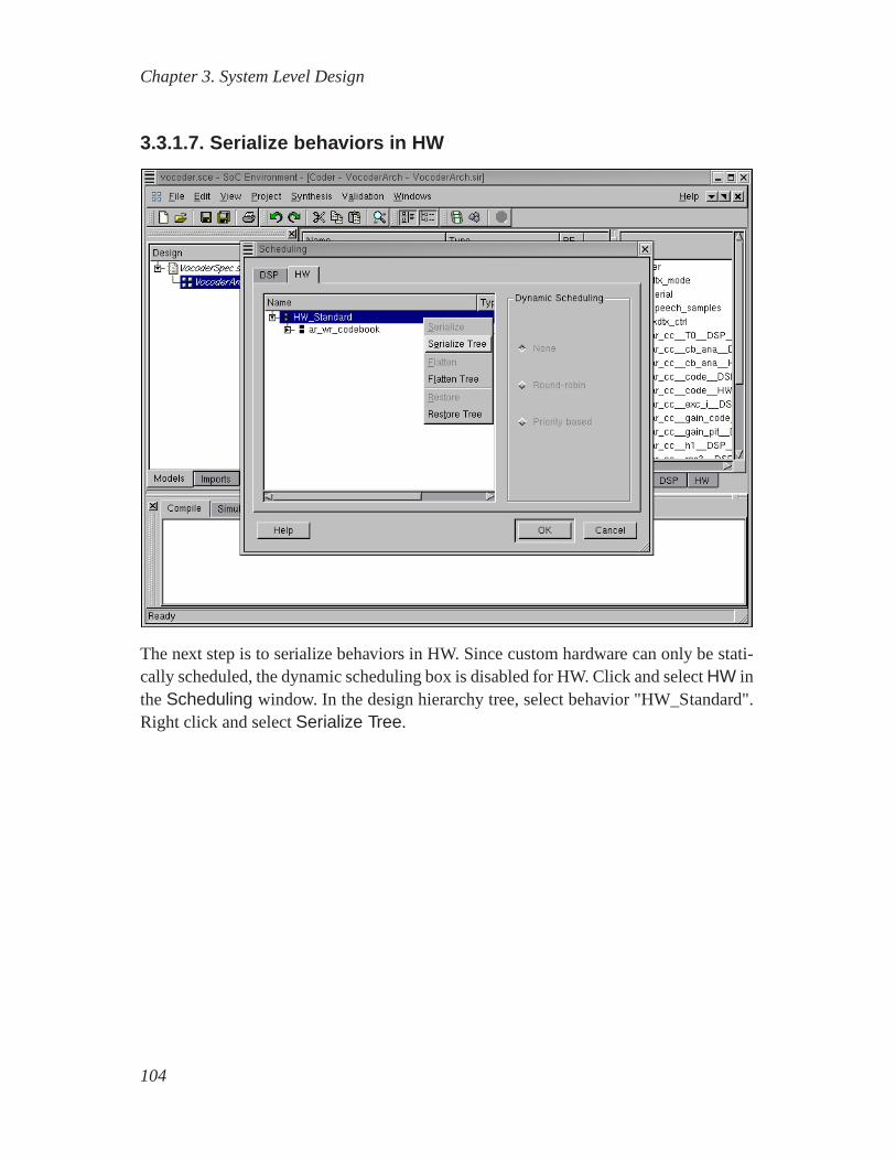
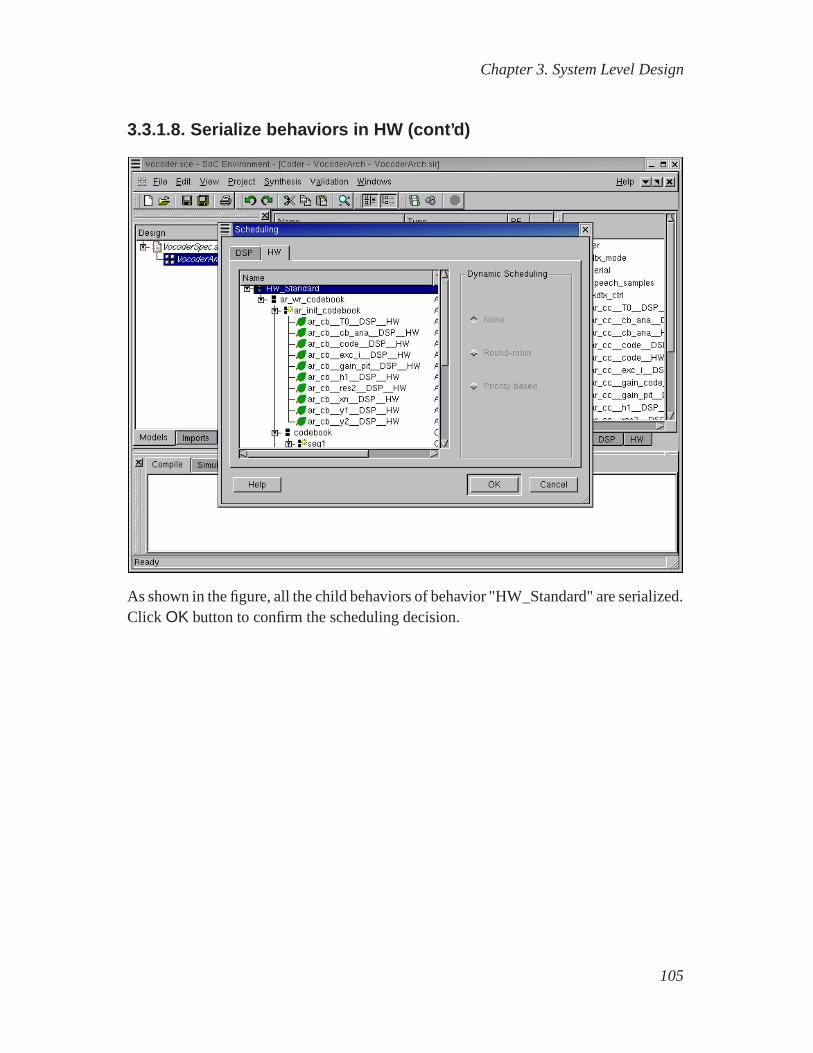
The next step is to serialize behaviors in HW. Since custom hardware can only be stati-cally scheduled, the dynamic scheduling box is disabled forHW. Click and selectHW intheScheduling window. In the design hierarchy tree, select behavior "HW_Standard".Right click and selectSerialize Tree.
104
Chapter 3. System Level Design
3.3.1.8. Serialize behaviors in HW (cont’d)
As shown in the figure, all the child behaviors of behavior "HW_Standard" are serialized.Click OK button to confirm the scheduling decision.
105
Chapter 3. System Level Design
3.3.2. Generate serialized model
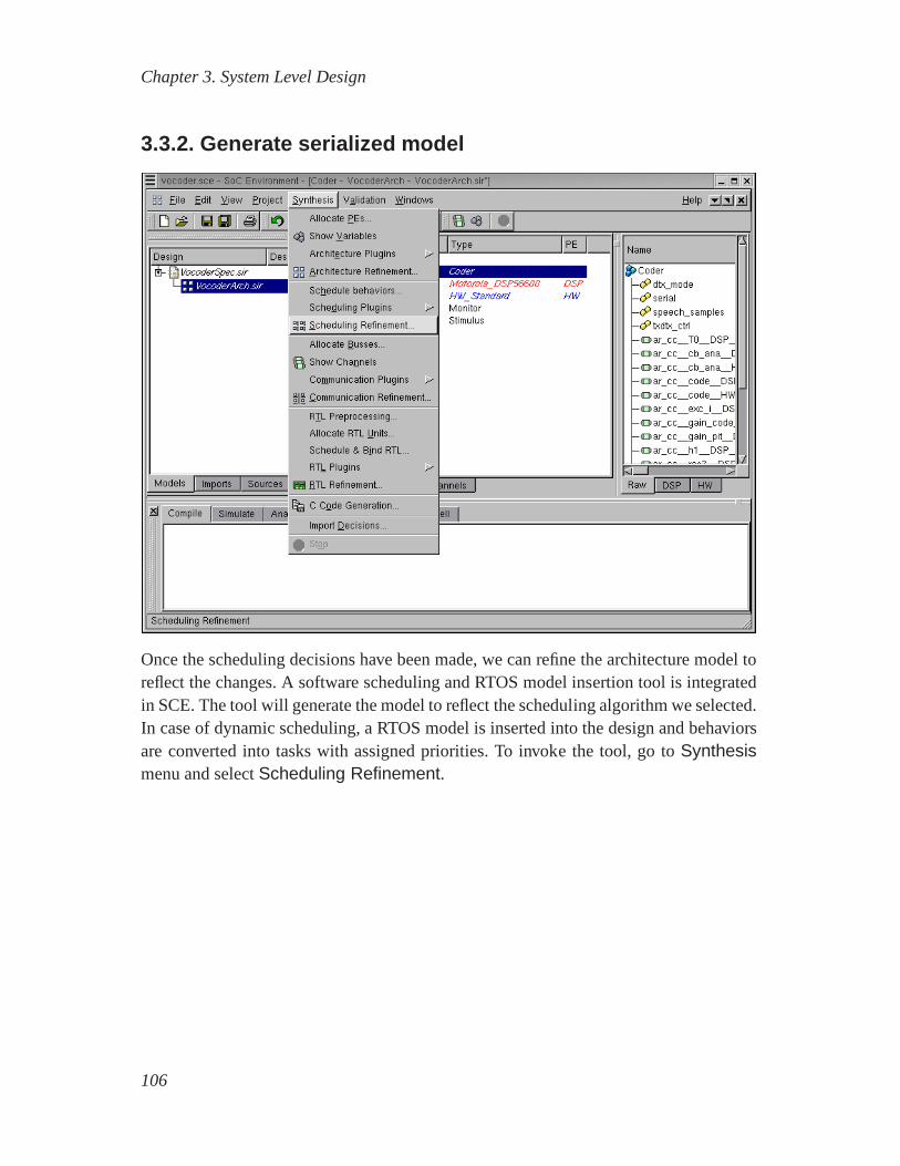
Once the scheduling decisions have been made, we can refine the architecture model toreflect the changes. A software scheduling and RTOS model insertion tool is integratedin SCE. The tool will generate the model to reflect the scheduling algorithm we selected.In case of dynamic scheduling, a RTOS model is inserted into the design and behaviorsare converted into tasks with assigned priorities. To invoke the tool, go toSynthesismenu and selectScheduling Refinement.
106
Chapter 3. System Level Design
3.3.2.1. Refine after serialization
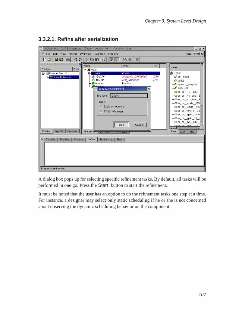
A dialog box pops up for selecting specific refinement tasks. By default, all tasks will beperformed in one go. Press theStart button to start the refinement.
It must be noted that the user has an option to do the refinementtasks one step at a time.For instance, a designer may select only static scheduling if he or she is not concernedabout observing the dynamic scheduling behavior on the component.
107

Chapter 3. System Level Design
3.3.2.2. Refine after serialization (cont’d)
The logging window shows the refinement process. After the refinement, the newly gen-erated serialized model "VocoderArch.sched.sir" is displayed to the design window. Itis also added to the current project window, under the architecture model "Vocoder-Arch.sir" to indicate that it was derived from "VocoderArch.sir".
108
Chapter 3. System Level Design
3.3.2.3. Refine after serialization (cont’d)
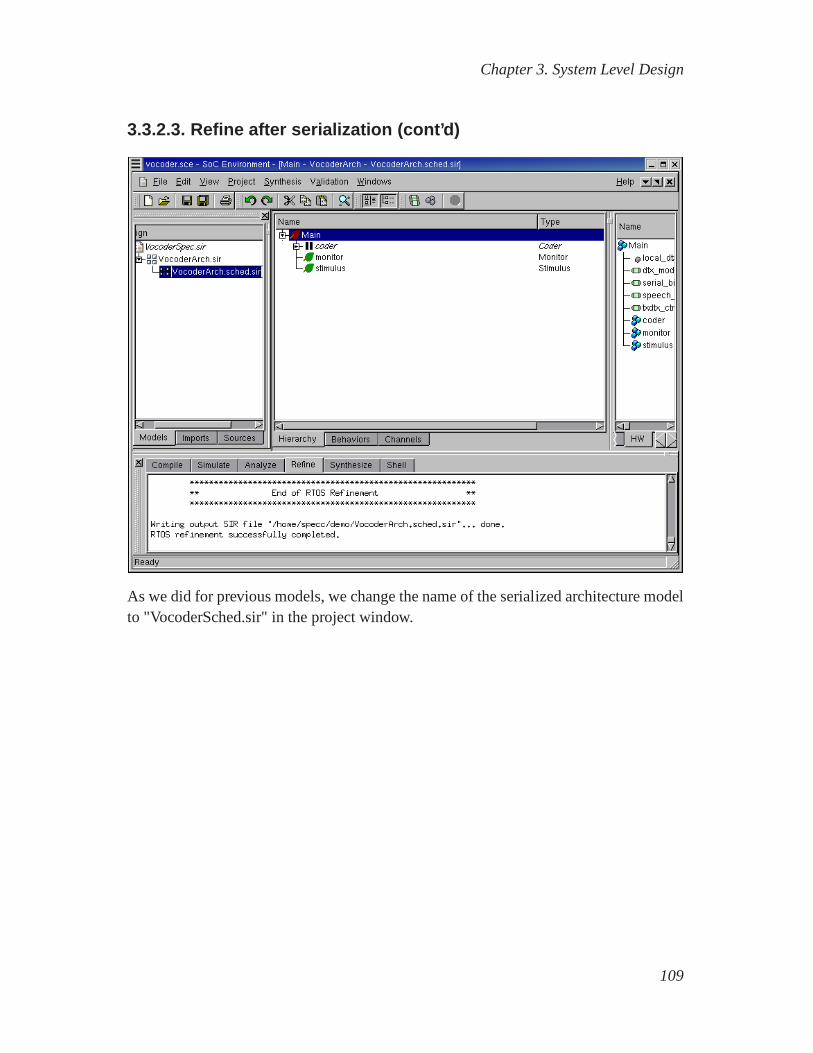
As we did for previous models, we change the name of the serialized architecture modelto "VocoderSched.sir" in the project window.
109

Chapter 3. System Level Design
3.3.3. Simulate serialized model (optional)
This section shows the simulation of the generated model. Ifthe readeris not interested, she or he can skip this section and go directly toSection 3.4Communication Synthesis(page 113).
Serialization refinement is now complete with the generation of a new model. However,we also need to confirm that the model has not lost any of its functionality in the re-finement process. In other words the new model must be functionally equivalent to thearchitecture model.
We will validate the serialized architecture model throughsimulation. But first we needto compile the model into an executable. To compile the serialized architecture model toexecutable, go toValidation menu and selectCompile.
110
Chapter 3. System Level Design
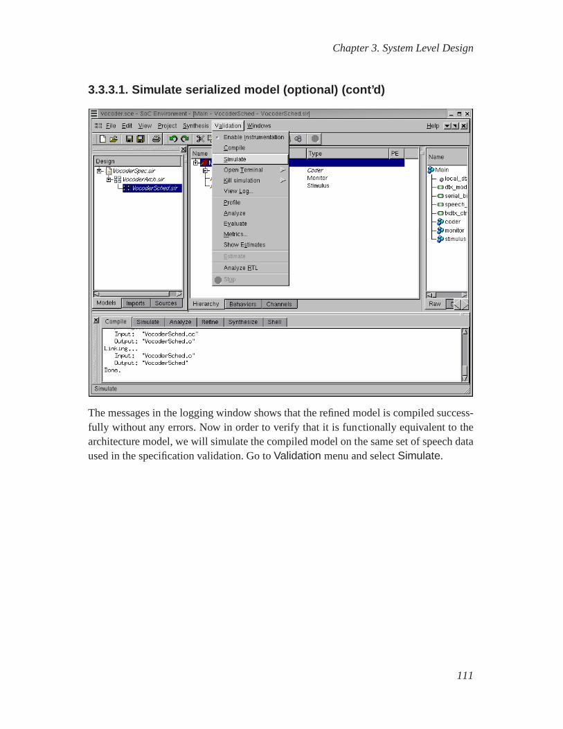
3.3.3.1. Simulate serialized model (optional) (cont’d)
The messages in the logging window shows that the refined model is compiled success-fully without any errors. Now in order to verify that it is functionally equivalent to thearchitecture model, we will simulate the compiled model on the same set of speech dataused in the specification validation. Go toValidation menu and selectSimulate.
111
Chapter 3. System Level Design
3.3.3.2. Simulate serialized model (optional) (cont’d)
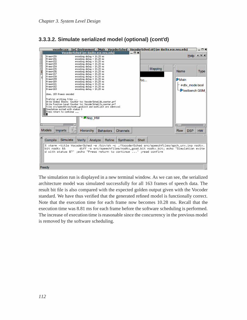
The simulation run is displayed in a new terminal window. As we can see, the serializedarchitecture model was simulated successfully for all 163 frames of speech data. Theresult bit file is also compared with the expected golden output given with the Vocoderstandard. We have thus verified that the generated refined model is functionally correct.Note that the execution time for each frame now becomes 10.28ms. Recall that theexecution time was 8.81 ms for each frame before the softwarescheduling is performed.The increase of execution time is reasonable since the concurrency in the previous modelis removed by the software scheduling.
112

Chapter 3. System Level Design
3.4. Communication SynthesisCommunication synthesis is the second part of the system level synthesis process. It re-fines the abstract communication between components in the architecture model. Specif-ically, the communication with variable channels is refinedinto an actual implementa-tion over wires of the system bus. The steps involved in this process are as follows.
We begin with allocation of system buses and selection of busprotocols. A set of systembuses is selected out of the bus library and the connectivityof the components withsystem buses is defined. In other words, we determine a bus architecture for our design.
This is followed by grouping of abstract variable channels.The communication betweensystem components has to be implemented with busses insteadof variable channels.Thus these channels are grouped and assigned to the chosen system busses. Once thisis done, the automatic refinement tool produces the requiredbus drivers for each com-ponent. It also divides variables into slices whose size is the same as width of the databus. Therefore that each slice can be sent or received using the bus protocol. The entirevariable is sent or received using multiple transfers of these slices.
113
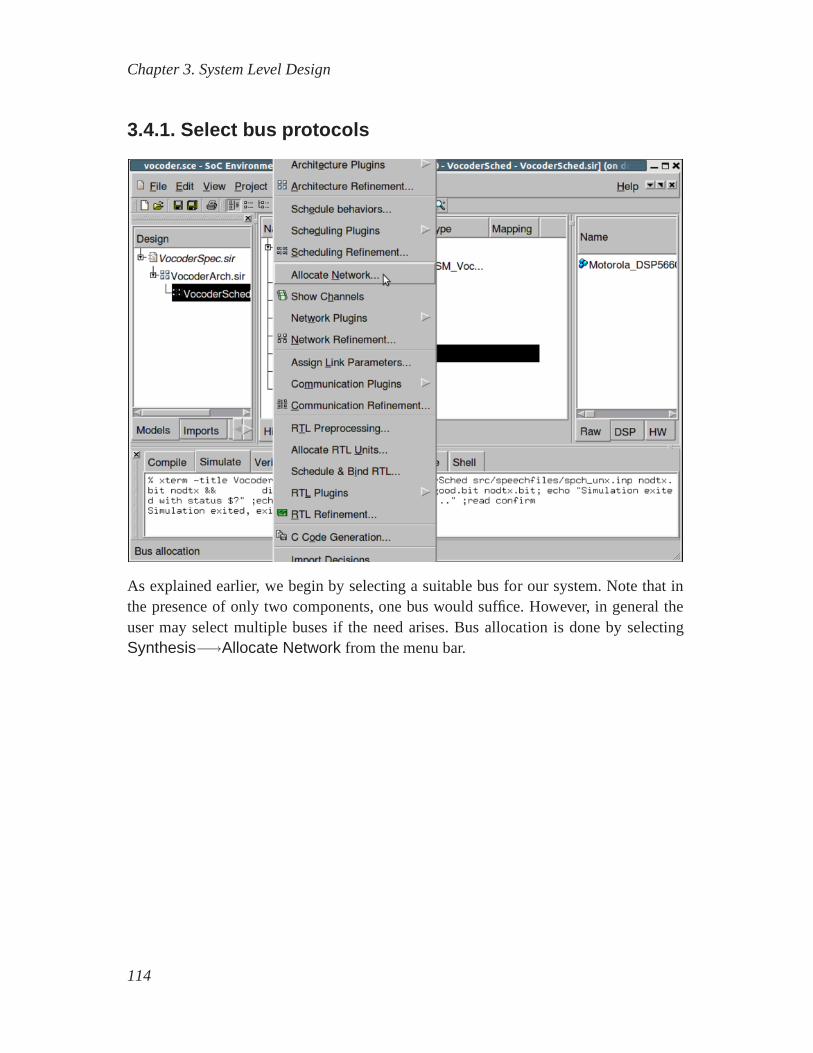
Chapter 3. System Level Design
3.4.1. Select bus protocols
As explained earlier, we begin by selecting a suitable bus for our system. Note that inthe presence of only two components, one bus would suffice. However, in general theuser may select multiple buses if the need arises. Bus allocation is done by selectingSynthesis−→Allocate Network from the menu bar.
114
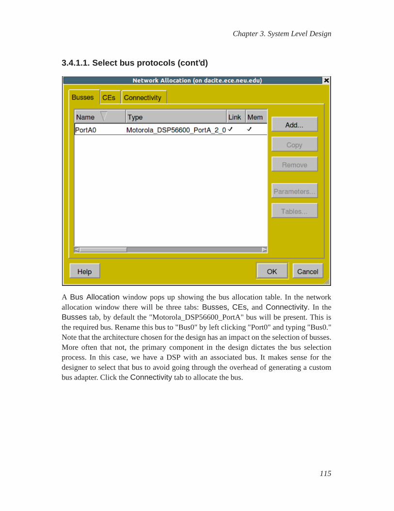
Chapter 3. System Level Design
3.4.1.1. Select bus protocols (cont’d)
A Bus Allocation window pops up showing the bus allocation table. In the networkallocation window there will be three tabs:Busses, CEs, andConnectivity. In theBusses tab, by default the "Motorola_DSP56600_PortA" bus will be present. This isthe required bus. Rename this bus to "Bus0" by left clicking "Port0" and typing "Bus0."Note that the architecture chosen for the design has an impact on the selection of busses.More often that not, the primary component in the design dictates the bus selectionprocess. In this case, we have a DSP with an associated bus. Itmakes sense for thedesigner to select that bus to avoid going through the overhead of generating a custombus adapter. Click theConnectivity tab to allocate the bus.
115
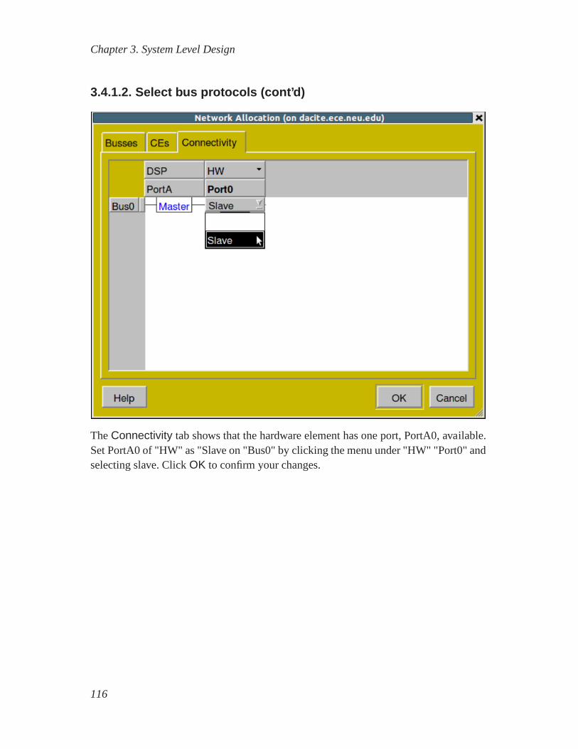
Chapter 3. System Level Design
3.4.1.2. Select bus protocols (cont’d)
TheConnectivity tab shows that the hardware element has one port, PortA0, available.Set PortA0 of "HW" as "Slave on "Bus0" by clicking the menu under "HW" "Port0" andselecting slave. ClickOK to confirm your changes.
116

Chapter 3. System Level Design
3.4.2. Map channels to buses
Once the bus allocation has been done, we need to group the channels of the architecturemodel and assign them to the system buses. Recall that in the architecture model, we hadcommunication between components with abstract variable channels. We now have toassign those variable channels to the system bus.
Expand the design hierarchy window and scroll to the right tofind a new column entryBus.
117
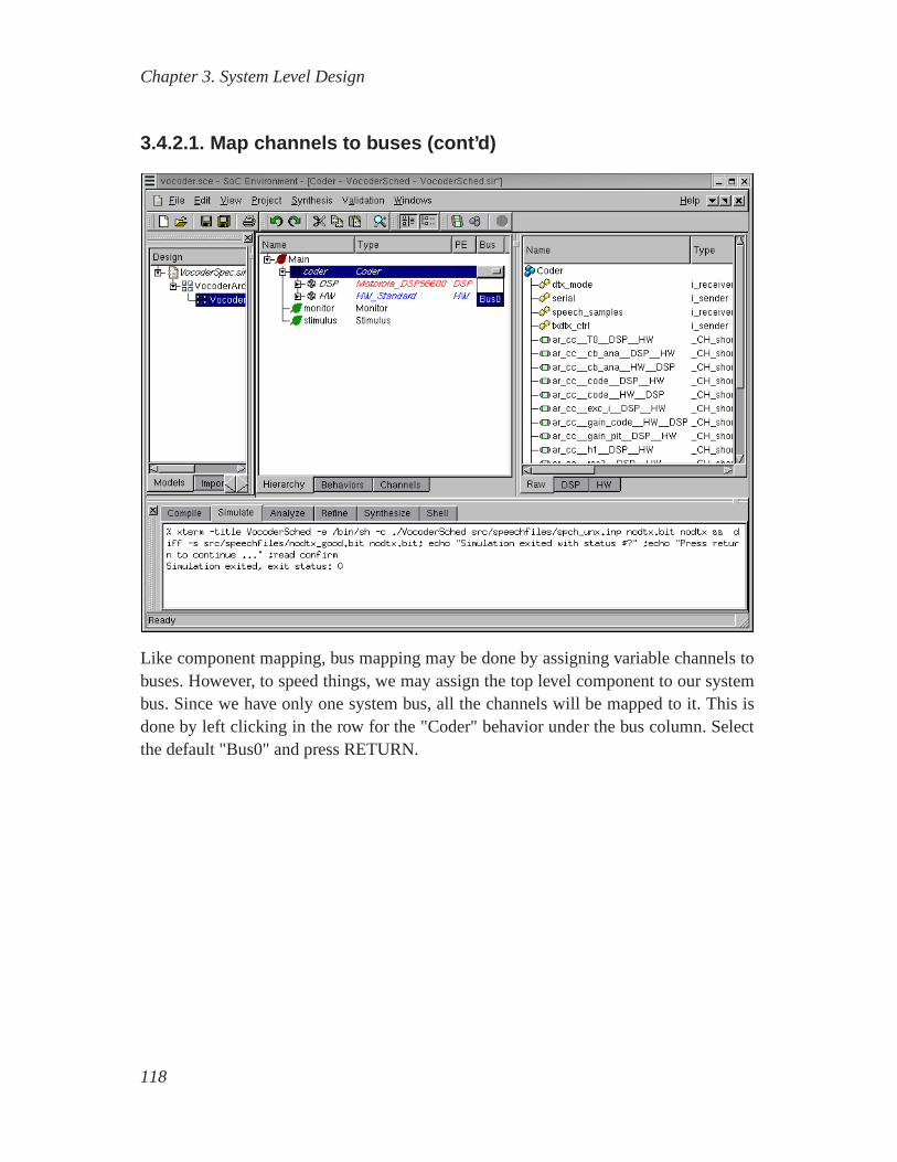
Chapter 3. System Level Design
3.4.2.1. Map channels to buses (cont’d)
Like component mapping, bus mapping may be done by assigningvariable channels tobuses. However, to speed things, we may assign the top level component to our systembus. Since we have only one system bus, all the channels will be mapped to it. This isdone by left clicking in the row for the "Coder" behavior under the bus column. Selectthe default "Bus0" and press RETURN.
118
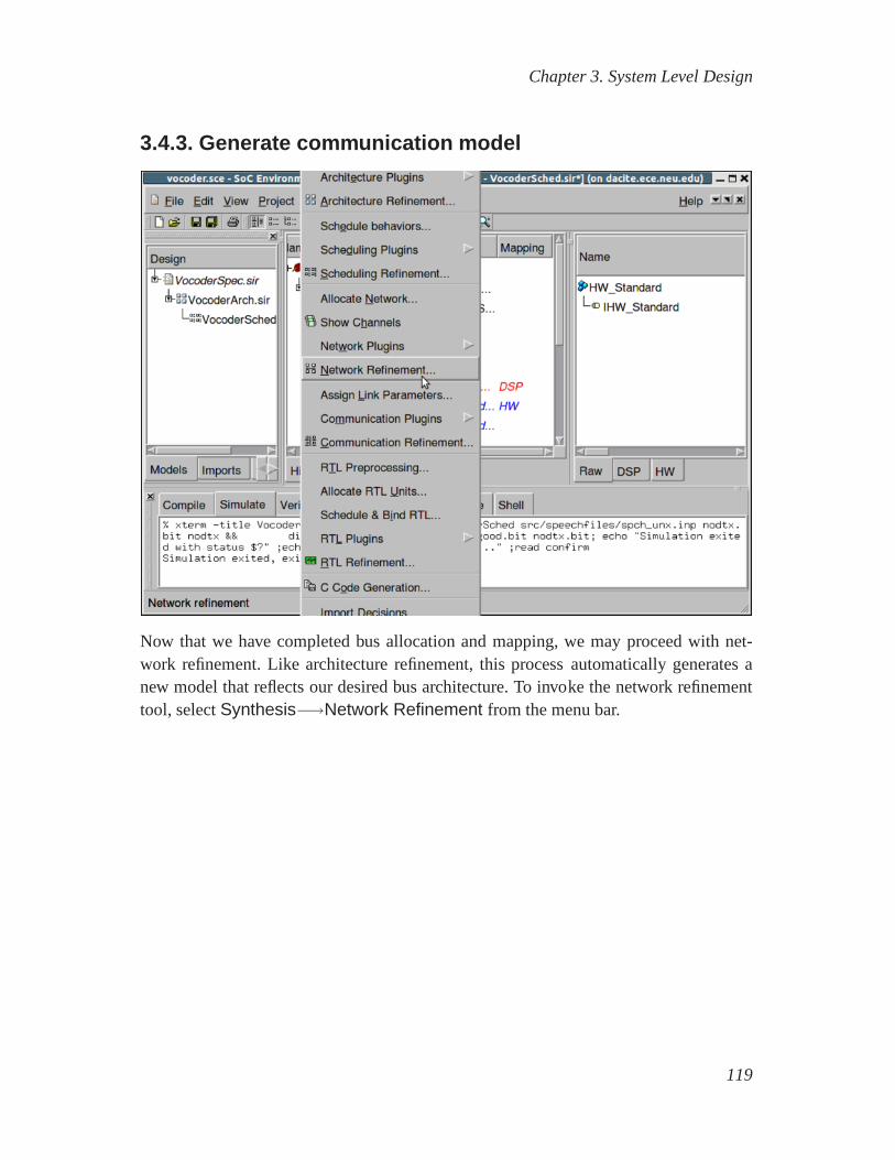
Chapter 3. System Level Design
3.4.3. Generate communication model
Now that we have completed bus allocation and mapping, we mayproceed with net-work refinement. Like architecture refinement, this processautomatically generates anew model that reflects our desired bus architecture. To invoke the network refinementtool, selectSynthesis−→Network Refinement from the menu bar.
119

Chapter 3. System Level Design
3.4.3.1. Generate communication model (cont’d)
A new window pops up giving the user the option to perform various stages of therefinement. The user may choose to partially refine the model without actually insertingthe bus, and only selecting the channel refinement phase. This way, he can play aroundwith different channel partitions. Likewise, the user might want to play around withdifferent bus protocols while avoiding "Inlining" them into components. This way hecan plug and play with different protocols before generating the final inlined model.By default all the stages are performed to produce the final communication refinement.Since we have only one bus, and hence a default mapping, we optfor all three stagesand left click onStart to proceed.
120
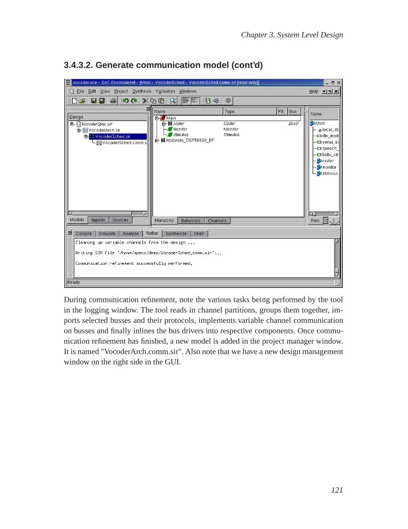
Chapter 3. System Level Design
3.4.3.2. Generate communication model (cont’d)
During communication refinement, note the various tasks being performed by the toolin the logging window. The tool reads in channel partitions,groups them together, im-ports selected busses and their protocols, implements variable channel communicationon busses and finally inlines the bus drivers into respectivecomponents. Once commu-nication refinement has finished, a new model is added in the project manager window.It is named "VocoderArch.comm.sir". Also note that we have anew design managementwindow on the right side in the GUI.
121
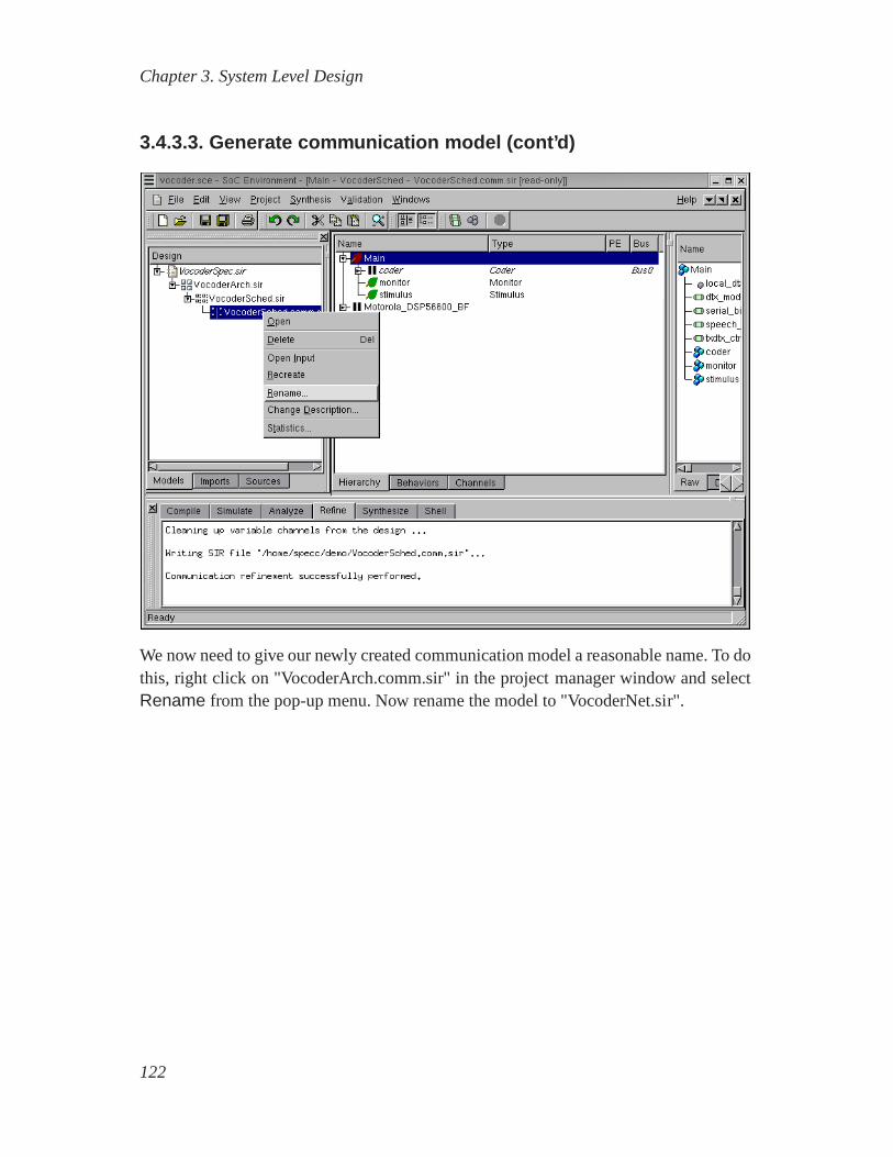
Chapter 3. System Level Design
3.4.3.3. Generate communication model (cont’d)
We now need to give our newly created communication model a reasonable name. To dothis, right click on "VocoderArch.comm.sir" in the projectmanager window and selectRename from the pop-up menu. Now rename the model to "VocoderNet.sir".
122
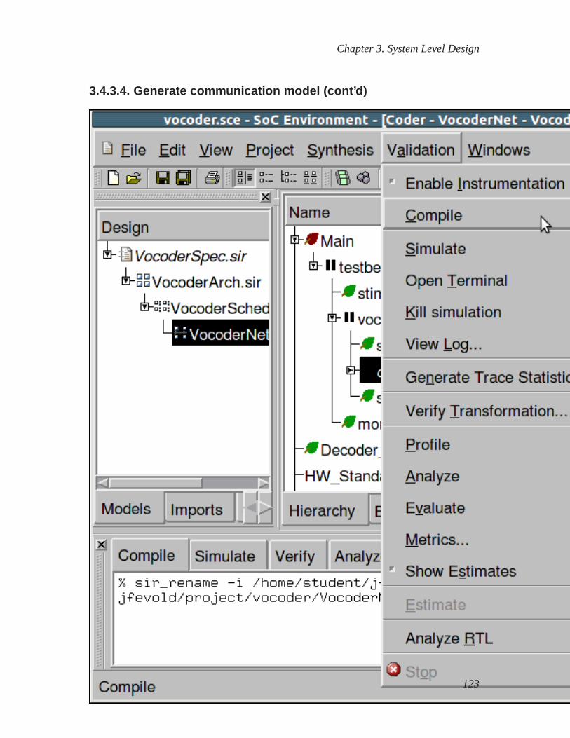
Chapter 3. System Level Design
3.4.3.4. Generate communication model (cont’d)
123

Chapter 3. System Level Design
Simulate the resulting network model of the design by selectingValidation−→Compile. Upon completion, selectValidation−→Simulate to validateits correctness.
124
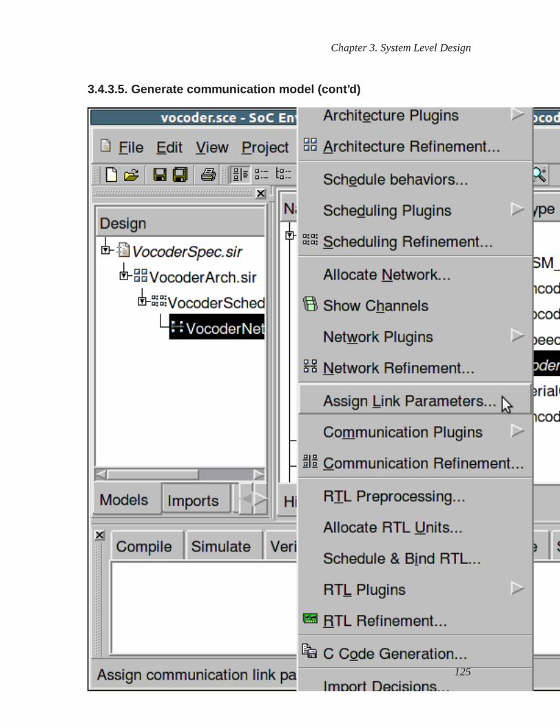
Chapter 3. System Level Design
3.4.3.5. Generate communication model (cont’d)
125

Chapter 3. System Level Design
After network refinement, synthesis of communication in each bus segment of the sys-tem has to be done to complete the communication design process. For this, we start bysetting parameters for all comunication links in the system. SelectSynthesis−→AssignLink Parameters.
126
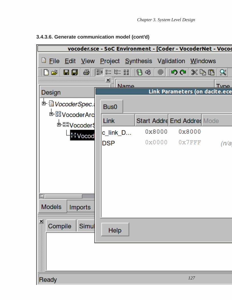
Chapter 3. System Level Design
3.4.3.6. Generate communication model (cont’d)
127
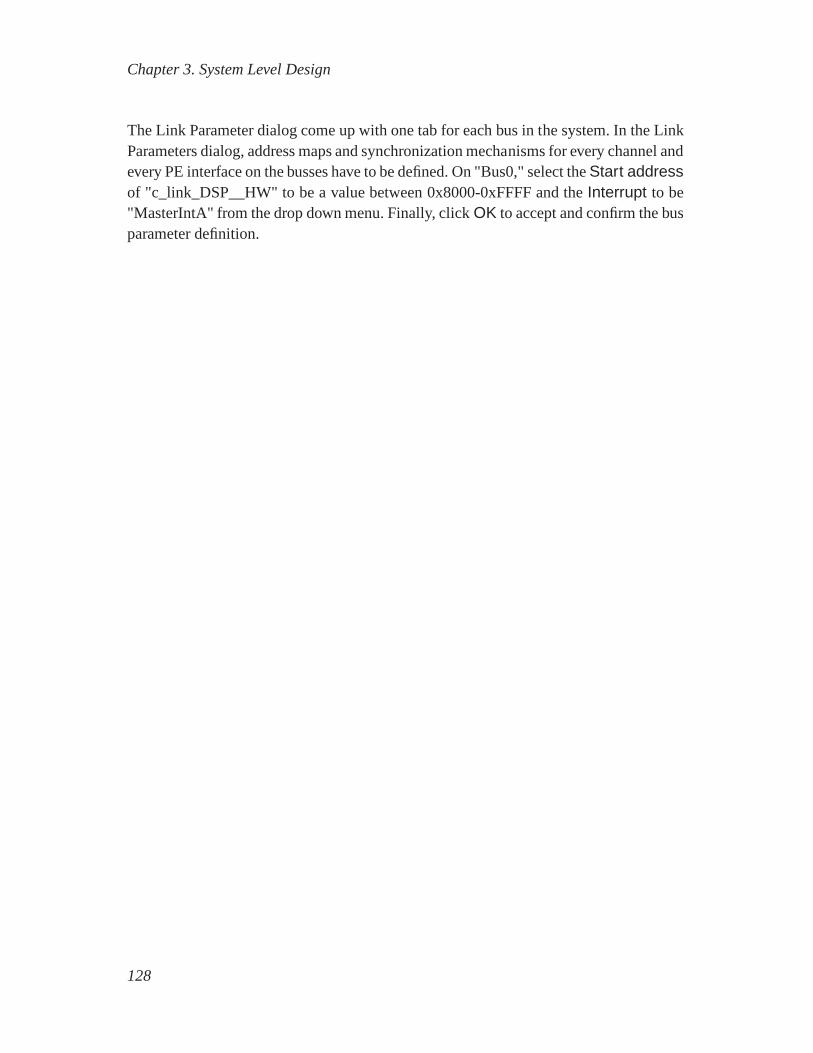
Chapter 3. System Level Design
The Link Parameter dialog come up with one tab for each bus in the system. In the LinkParameters dialog, address maps and synchronization mechanisms for every channel andevery PE interface on the busses have to be defined. On "Bus0,"select theStart addressof "c_link_DSP__HW" to be a value between 0x8000-0xFFFF andthe Interrupt to be"MasterIntA" from the drop down menu. Finally, clickOK to accept and confirm the busparameter definition.
128

Chapter 3. System Level Design
3.4.3.7. Generate communication model (cont’d)
129

Chapter 3. System Level Design
SelectSynthesis−→Communication Refinement to invoke the final communicationrefinement tool.
130
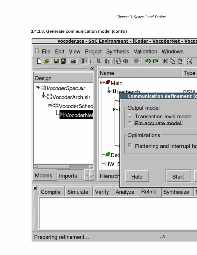
Chapter 3. System Level Design
3.4.3.8. Generate communication model (cont’d)
131

Chapter 3. System Level Design
The dialog that pops up provides the option either to generate aPin Accurate Modelor aTransaction Level Model of the design. Accept the default option of generating aPAM and clickStart to proceed.
132
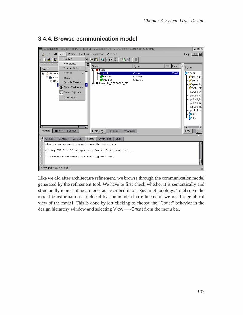
Chapter 3. System Level Design
3.4.4. Browse communication model
Like we did after architecture refinement, we browse throughthe communication modelgenerated by the refinement tool. We have to first check whether it is semantically andstructurally representing a model as described in our SoC methodology. To observe themodel transformations produced by communication refinement, we need a graphicalview of the model. This is done by left clicking to choose the "Coder" behavior in thedesign hierarchy window and selectingView−→Chart from the menu bar.
133
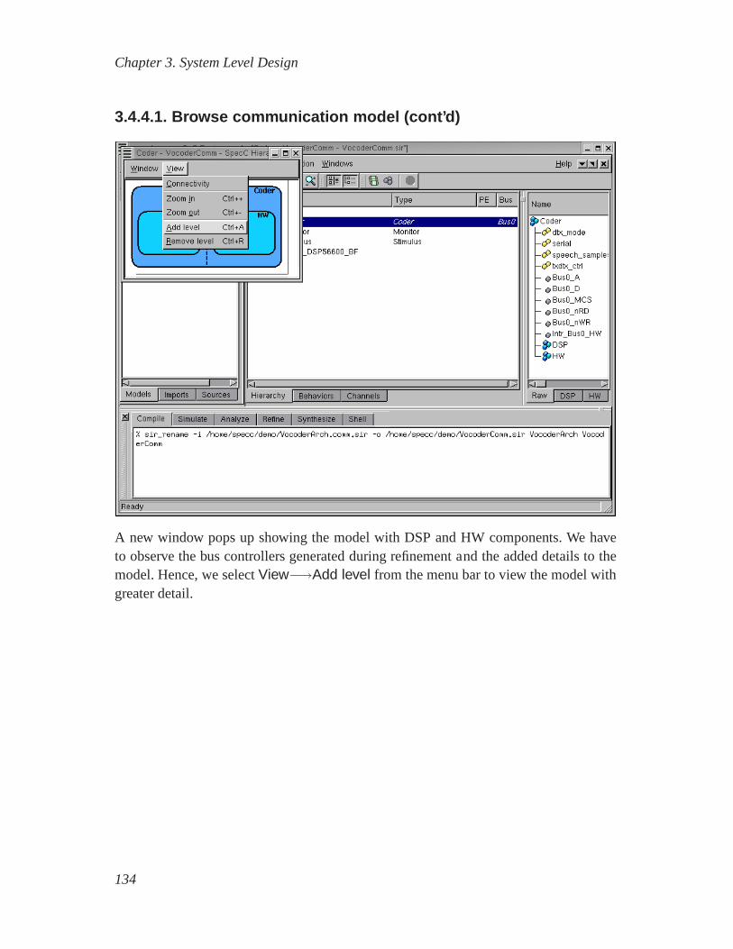
Chapter 3. System Level Design
3.4.4.1. Browse communication model (cont’d)
A new window pops up showing the model with DSP and HW components. We haveto observe the bus controllers generated during refinement and the added details to themodel. Hence, we selectView−→Add level from the menu bar to view the model withgreater detail.
134
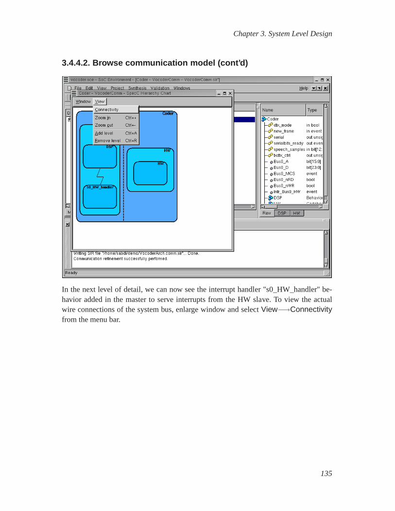
Chapter 3. System Level Design
3.4.4.2. Browse communication model (cont’d)
In the next level of detail, we can now see the interrupt handler "s0_HW_handler" be-havior added in the master to serve interrupts from the HW slave. To view the actualwire connections of the system bus, enlarge window and select View−→Connectivityfrom the menu bar.
135

Chapter 3. System Level Design
3.4.4.3. Browse communication model (cont’d)
The wire level detail of the connection between components can now be seen in thewindow. Note that the system bus wires are distinguished by green boxes. Hence we seethat the bus is introduced in the design and the individual components are connectedwith the bus instead of the abstract variable channels. On observing the hierarchicalview further, we can see the drivers in each components. These drivers take the originalvariables and implement the high-level send/receive methods using the bus protocol.
We have thus seen that the structure of communication model follows the semantics ofthe model explained in our methodology. We may complete the browsing session byselectingWindow−→Close from the menu bar.
136
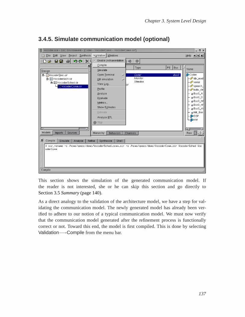
Chapter 3. System Level Design
3.4.5. Simulate communication model (optional)
This section shows the simulation of the generated communication model. Ifthe reader is not interested, she or he can skip this section and go directly toSection 3.5Summary(page 140).
As a direct analogy to the validation of the architecture model, we have a step for val-idating the communication model. The newly generated modelhas already been ver-ified to adhere to our notion of a typical communication model. We must now verifythat the communication model generated after the refinementprocess is functionallycorrect or not. Toward this end, the model is first compiled. This is done by selectingValidation−→Compile from the menu bar.
137

Chapter 3. System Level Design
3.4.5.1. Simulate communication model (optional) (cont’d )
The model should compile without errors and this may be observed in the logging win-dow. Once the model has successfully compiled, we must proceed to simulate it. This isdone by selectingValidation−→Simulate from the menu bar.
138
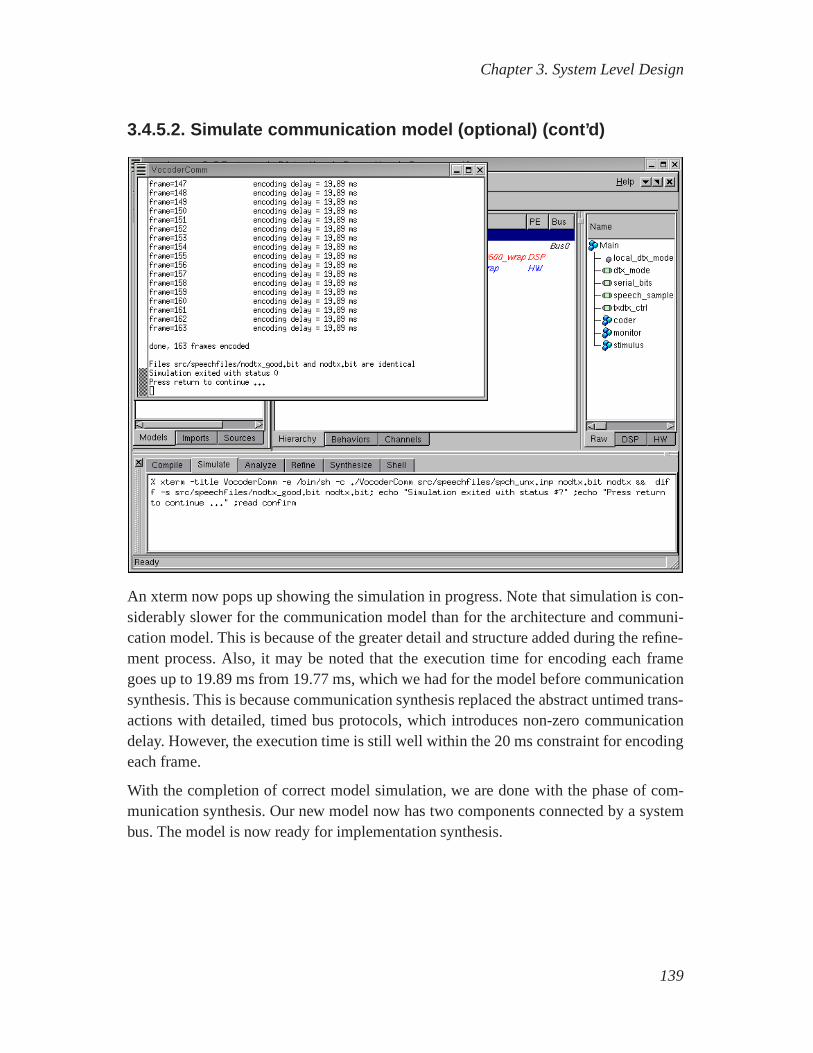
Chapter 3. System Level Design
3.4.5.2. Simulate communication model (optional) (cont’d )
An xterm now pops up showing the simulation in progress. Notethat simulation is con-siderably slower for the communication model than for the architecture and communi-cation model. This is because of the greater detail and structure added during the refine-ment process. Also, it may be noted that the execution time for encoding each framegoes up to 19.89 ms from 19.77 ms, which we had for the model before communicationsynthesis. This is because communication synthesis replaced the abstract untimed trans-actions with detailed, timed bus protocols, which introduces non-zero communicationdelay. However, the execution time is still well within the 20 ms constraint for encodingeach frame.
With the completion of correct model simulation, we are donewith the phase of com-munication synthesis. Our new model now has two components connected by a systembus. The model is now ready for implementation synthesis.
139
Chapter 3. System Level Design
3.5. SummaryIn this chapter, we covered the system level design phase of our methodology. With therise in level of abstraction in system specification, it is nolonger feasible to start designsat cycle accurate level. Instead, the specification should be gradually refined to derive acycle accurate model. We saw three major steps in the system level design and synthesisprocess.
Architecture refinement took in the system specification model as input. Based on theprofile of the specification, we chose the appropriate components to implement the de-sired system. We also delved into design space exploration by seeking a purely softwaresolution. When the software solution turned out to be infeasible, we added a HW com-ponent to meet the real-time constraint of the design. We also demonstrated the power ofautomatic refinement to quickly come up with models and evaluate them, thereby greatlyenhancing design space exploration. In the future, we will look at how to automate thedecision making process, so that the tool can propose an optimal system architecturebased on system constraints and available components.
Architecture refinement was followed by software scheduling and the RTOS insertionstep. Although, for this demo, we did not need to insert any RTOS, it is a feature avail-able in SCE. It allows for inclusion of useful task scheduling algorithms for dynamicscheduling. We also provide for static scheduling of tasks on both HW and SW.
The final major step of system level design is communication synthesis. We showed howthe designer can use the database of a variety of bus models toconstruct a communica-tion architecture for the design. Once the communication architecture is complete, thedesigners can assign abstract data transfers to a communication route in the architecture.Using automatic refinement in SCE, we showed how the designercould quickly producea bus functional communication model and see if it fits the system requirements. Thisbus functional model serves as an input to the tasks of customHW generation and SWcode generation, which are described in the next two chapter. In the future, we wouldlike to enhance the capabilities of our tool to perform automatic communication syn-thesis, whereby the tool can generate a good communication architecture and still meetsystem specification constraints.
140
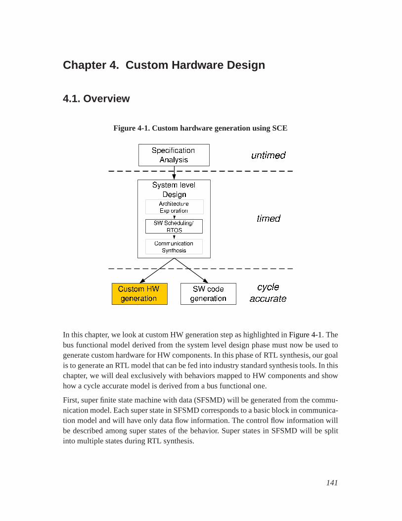
Chapter 4. Custom Hardware Design
4.1. Overview
Figure 4-1. Custom hardware generation using SCE
In this chapter, we look at custom HW generation step as highlighted inFigure 4-1. Thebus functional model derived from the system level design phase must now be used togenerate custom hardware for HW components. In this phase ofRTL synthesis, our goalis to generate an RTL model that can be fed into industry standard synthesis tools. In thischapter, we will deal exclusively with behaviors mapped to HW components and showhow a cycle accurate model is derived from a bus functional one.
First, super finite state machine with data (SFSMD) will be generated from the commu-nication model. Each super state in SFSMD corresponds to a basic block in communica-tion model and will have only data flow information. The control flow information willbe described among super states of the behavior. Super states in SFSMD will be splitinto multiple states during RTL synthesis.
141

Chapter 4. Custom Hardware Design
Second, the RTL units for the custom hardware are allocated.To get some informa-tion like number of operations, number of variables and number of data transfers in theSFSMD for the RTL allocation, the designer has to run RTL analysis tool.
Third, scheduling and binding is done by designer or by tools. The scheduling and bind-ing information will be inserted into the SFSMD model.
Finally, the SFSMD model with scheduling and binding information is refined into acycle-accurate FSMD model by RTL refinement tool. The refinement tool will also ger-erate a cycle accurate model in hardware description languages like Verilog and Handel-C. The cycle accurate model in Verilog HDL can be used as inputto commercial logicsynthesis tools like Synopsys Design Compiler. We also generate the cycle-accuratemodel in Handel-C which can be fed into Celoxica Design Kit.
142
Chapter 4. Custom Hardware Design
4.2. RTL PreprocessingIn our design methodology, RTL design is modeled by Finite State Machine with Data(FSMD) which finite state machine model with assignment statements added to eachstates. The FSMD can completely specify the behavior of an arbitrary RTL design.
In this tutorial, we use an intermediate representation, super finite state machine withdata (SFSMD), where each state may take more than one cycle toexecute. The SF-SMD will be automatically refined into cycle-accurate FSMD after RTL scheduling andbinding.
143

Chapter 4. Custom Hardware Design
4.2.1. View behavioral input model
Before we show how to generate SFSMD, we take a look at how input model of customhardware design. Select the behavior "Build_Code" by left clicking on it. We can take alook at the behavioral input model by selectingView−→Source from the menu bar.
144

Chapter 4. Custom Hardware Design
4.2.1.1. View behavioral input model (cont’d)
The SpecC Editor window pops up showing the source code for behavior"Build_Code".
145
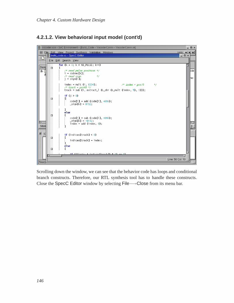
Chapter 4. Custom Hardware Design
4.2.1.2. View behavioral input model (cont’d)
Scrolling down the window, we can see that the behavior code has loops and conditionalbranch constructs. Therefore, our RTL synthesis tool has tohandle these constructs.Close theSpecC Editor window by selectingFile−→Close from its menu bar.
146
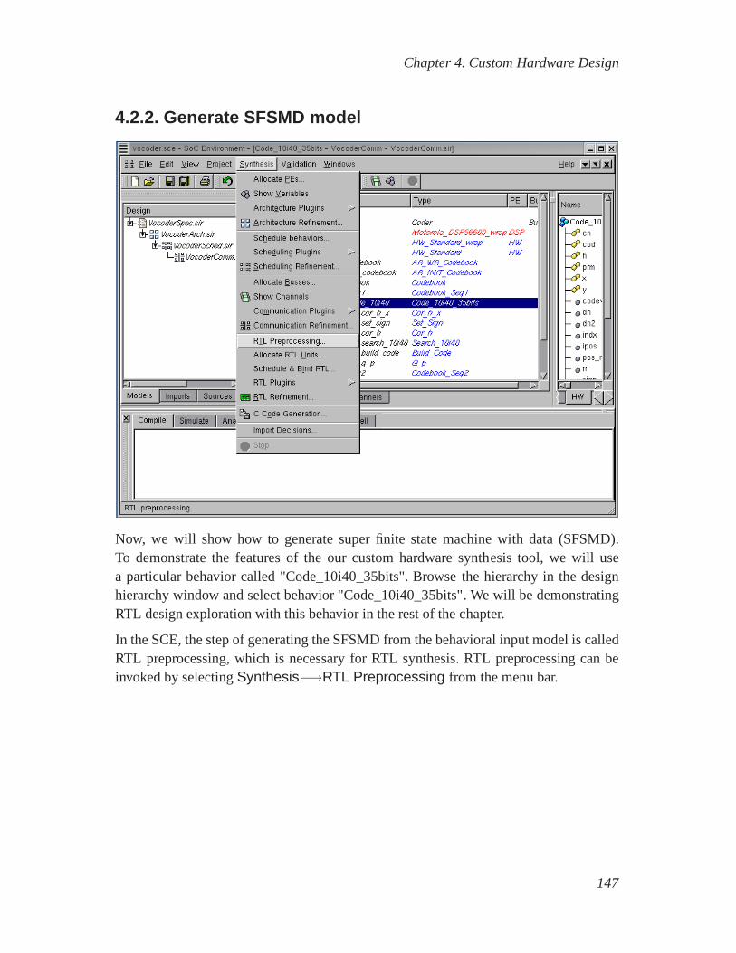
Chapter 4. Custom Hardware Design
4.2.2. Generate SFSMD model
Now, we will show how to generate super finite state machine with data (SFSMD).To demonstrate the features of the our custom hardware synthesis tool, we will usea particular behavior called "Code_10i40_35bits". Browsethe hierarchy in the designhierarchy window and select behavior "Code_10i40_35bits". We will be demonstratingRTL design exploration with this behavior in the rest of the chapter.
In the SCE, the step of generating the SFSMD from the behavioral input model is calledRTL preprocessing, which is necessary for RTL synthesis. RTL preprocessing can beinvoked by selectingSynthesis−→RTL Preprocessing from the menu bar.
147
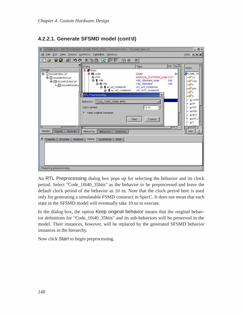
Chapter 4. Custom Hardware Design
4.2.2.1. Generate SFSMD model (cont’d)
An RTL Preprocessing dialog box pops up for selecting the behavior and its clockperiod. Select "Code_10i40_35bits" as the behavior to be preprocessed and leave thedefault clock period of the behavior as 10 ns. Note that the clock period here is usedonly for generating a simulatable FSMD construct in SpecC. It does not mean that eachstate in the SFSMD model will eventually take 10 ns to execute.
In the dialog box, the optionKeep original behavior means that the original behav-ior definitions for "Code_10i40_35bits" and its sub-behaviors will be preserved in themodel. Their instances, however, will be replaced by the generated SFSMD behaviorinstances in the hierarchy.
Now click Start to begin preprocessing.
148
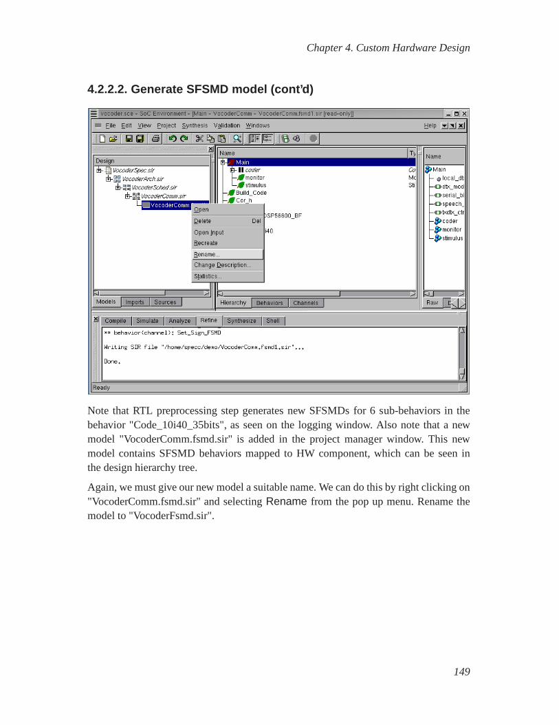
Chapter 4. Custom Hardware Design
4.2.2.2. Generate SFSMD model (cont’d)
Note that RTL preprocessing step generates new SFSMDs for 6 sub-behaviors in thebehavior "Code_10i40_35bits", as seen on the logging window. Also note that a newmodel "VocoderComm.fsmd.sir" is added in the project manager window. This newmodel contains SFSMD behaviors mapped to HW component, which can be seen inthe design hierarchy tree.
Again, we must give our new model a suitable name. We can do this by right clicking on"VocoderComm.fsmd.sir" and selectingRename from the pop up menu. Rename themodel to "VocoderFsmd.sir".
149
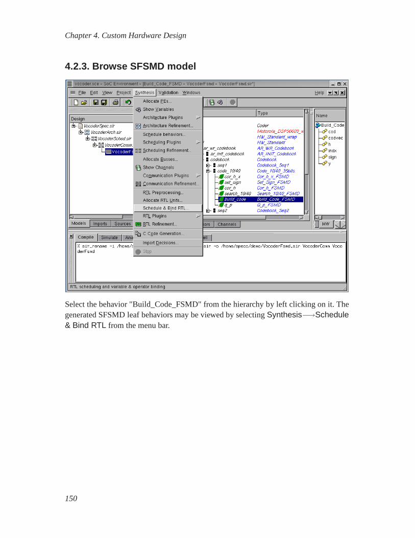
Chapter 4. Custom Hardware Design
4.2.3. Browse SFSMD model
Select the behavior "Build_Code_FSMD" from the hierarchy by left clicking on it. Thegenerated SFSMD leaf behaviors may be viewed by selectingSynthesis−→Schedule& Bind RTL from the menu bar.
150

Chapter 4. Custom Hardware Design
4.2.3.1. Browse SFSMD model (cont’d)
TheRTL Scheduling & Binding window pops up showing all the states in the behavior"Build_Code_FSMD". It also shows all statements for the selected state in the right-most column. We can go inside each state by clicking on the corresponding circle in theleft-most column. In this screen shot, state S9 is selected.We can see all assignmentswith operations and state transitions derived from "if" statements.
Left click onCancel to close RTL Scheduling & Binding window.
151
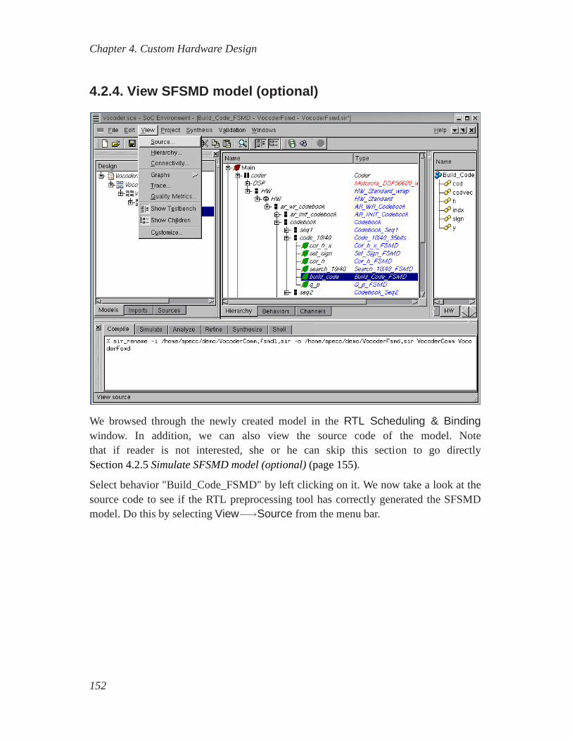
Chapter 4. Custom Hardware Design
4.2.4. View SFSMD model (optional)
We browsed through the newly created model in theRTL Scheduling & Bindingwindow. In addition, we can also view the source code of the model. Notethat if reader is not interested, she or he can skip this section to go directlySection 4.2.5Simulate SFSMD model (optional)(page 155).
Select behavior "Build_Code_FSMD" by left clicking on it. We now take a look at thesource code to see if the RTL preprocessing tool has correctly generated the SFSMDmodel. Do this by selectingView−→Source from the menu bar.
152
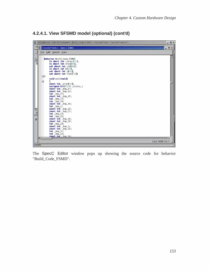
Chapter 4. Custom Hardware Design
4.2.4.1. View SFSMD model (optional) (cont’d)
The SpecC Editor window pops up showing the source code for behavior"Build_Code_FSMD".
153

Chapter 4. Custom Hardware Design
4.2.4.2. View SFSMD model (optional) (cont’d)
The behavioral input model is changed to the SFSMD model withclock period 10 ns.Scroll down the window to find loops and conditional branch constructs in the behavioralinput model are changed to state transitions. Still, each state has a lot of assignments andoperations, which have to be scheduled and bound.
Close theSpecC Editor window by selectingFile−→Close from the menu bar.
154

Chapter 4. Custom Hardware Design
4.2.5. Simulate SFSMD model (optional)
For demo purposes, we will skip the SFSMD generation of thoseother behaviors as-signed to HW component. Even this partially refined model is actually simulatable. Toshow this, first compile the model by selectingValidation−→Compile from the menubar.
If reader is not interested, she or he can skip this section togo directlySection 4.2.6Analyze SFSMD model(page 158).
155
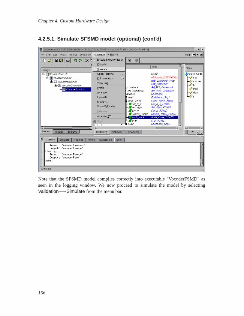
Chapter 4. Custom Hardware Design
4.2.5.1. Simulate SFSMD model (optional) (cont’d)
Note that the SFSMD model compiles correctly into executable "VocoderFSMD" asseen in the logging window. We now proceed to simulate the model by selectingValidation−→Simulate from the menu bar.
156
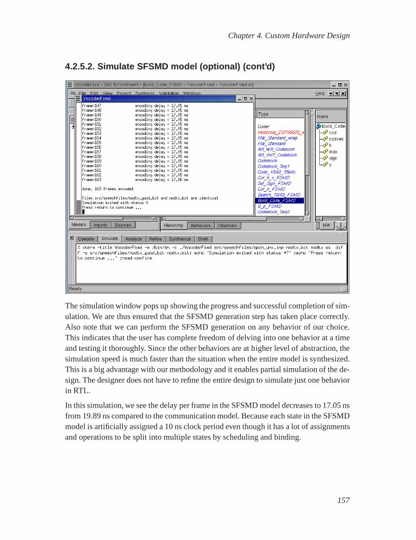
Chapter 4. Custom Hardware Design
4.2.5.2. Simulate SFSMD model (optional) (cont’d)
The simulation window pops up showing the progress and successful completion of sim-ulation. We are thus ensured that the SFSMD generation step has taken place correctly.Also note that we can perform the SFSMD generation on any behavior of our choice.This indicates that the user has complete freedom of delvinginto one behavior at a timeand testing it thoroughly. Since the other behaviors are at higher level of abstraction, thesimulation speed is much faster than the situation when the entire model is synthesized.This is a big advantage with our methodology and it enables partial simulation of the de-sign. The designer does not have to refine the entire design tosimulate just one behaviorin RTL.
In this simulation, we see the delay per frame in the SFSMD model decreases to 17.05 nsfrom 19.89 ns compared to the communication model. Because each state in the SFSMDmodel is artificially assigned a 10 ns clock period even though it has a lot of assignmentsand operations to be split into multiple states by scheduling and binding.
157
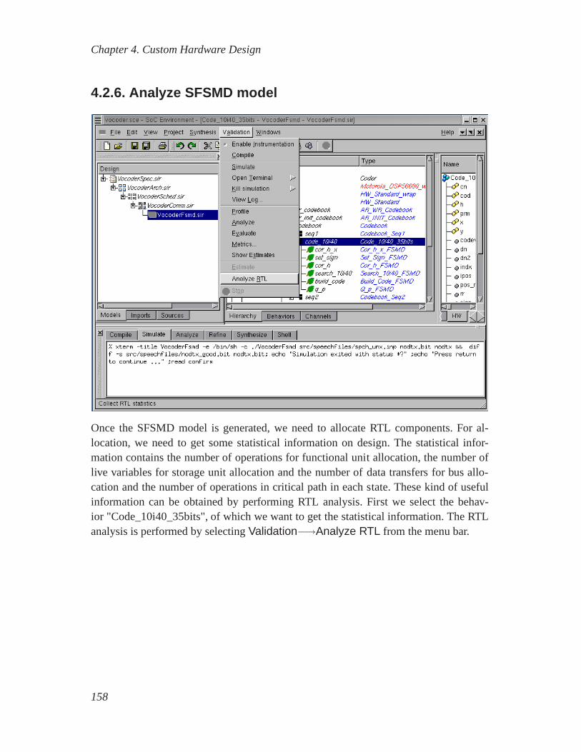
Chapter 4. Custom Hardware Design
4.2.6. Analyze SFSMD model
Once the SFSMD model is generated, we need to allocate RTL components. For al-location, we need to get some statistical information on design. The statistical infor-mation contains the number of operations for functional unit allocation, the number oflive variables for storage unit allocation and the number ofdata transfers for bus allo-cation and the number of operations in critical path in each state. These kind of usefulinformation can be obtained by performing RTL analysis. First we select the behav-ior "Code_10i40_35bits", of which we want to get the statistical information. The RTLanalysis is performed by selectingValidation−→Analyze RTL from the menu bar.
158
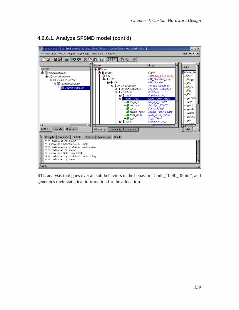
Chapter 4. Custom Hardware Design
4.2.6.1. Analyze SFSMD model (cont’d)
RTL analysis tool goes over all sub-behaviors in the behavior "Code_10i40_35bits", andgenerates their statistical information for the allocation.
159
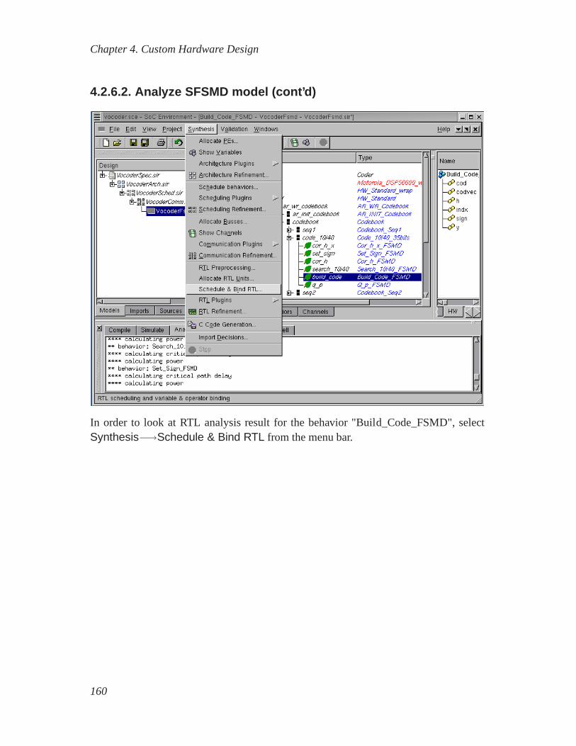
Chapter 4. Custom Hardware Design
4.2.6.2. Analyze SFSMD model (cont’d)
In order to look at RTL analysis result for the behavior "Build_Code_FSMD", selectSynthesis−→Schedule & Bind RTL from the menu bar.
160

Chapter 4. Custom Hardware Design
4.2.6.3. Analyze SFSMD model (cont’d)
TheRTL Scheduling & Binding window pops up showing the statistical informationfor the selected behavior. From left to right in the left panel of the RTL Scheduling &Binding window, it shows number of operations (Operations column) in each state,number of variables (Variables), number of data transfers (Transfers), number of oper-ations in critical path (Delay), and power dissipation (Power).
161
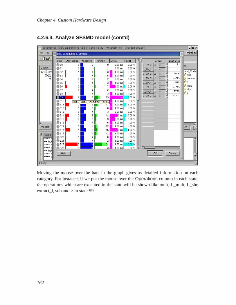
Chapter 4. Custom Hardware Design
4.2.6.4. Analyze SFSMD model (cont’d)
Moving the mouse over the bars in the graph gives us detailed information on eachcategory. For instance, if we put the mouse over theOperations column in each state,the operations which are executed in the state will be shown like mult, L_mult, L_shr,extract_l, sub and > in state S9.
162
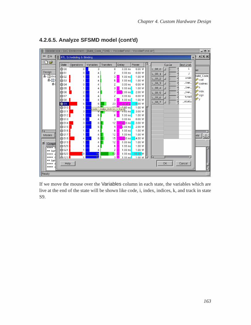
Chapter 4. Custom Hardware Design
4.2.6.5. Analyze SFSMD model (cont’d)
If we move the mouse over theVariables column in each state, the variables which arelive at the end of the state will be shown like code, i, index, indices, k, and track in stateS9.
163
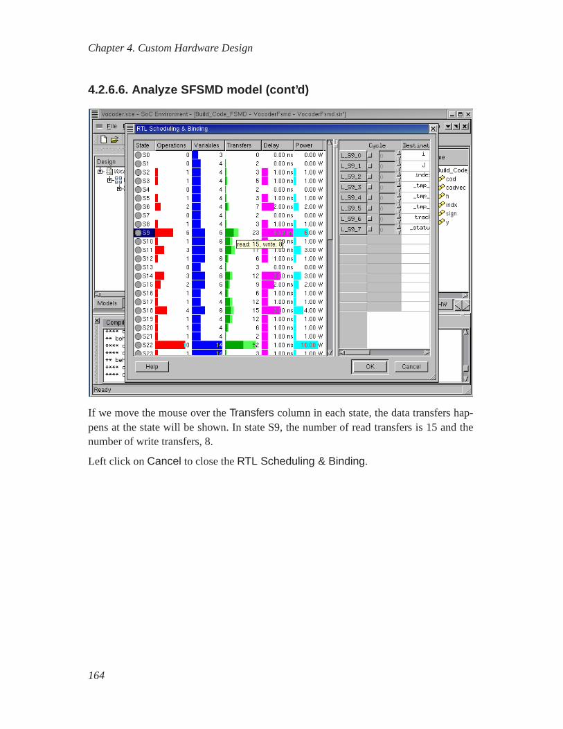
Chapter 4. Custom Hardware Design
4.2.6.6. Analyze SFSMD model (cont’d)
If we move the mouse over theTransfers column in each state, the data transfers hap-pens at the state will be shown. In state S9, the number of readtransfers is 15 and thenumber of write transfers, 8.
Left click onCancel to close theRTL Scheduling & Binding.
164
Chapter 4. Custom Hardware Design
4.3. RTL AllocationRTL allocation is one of important steps for custom hardwaredesign. It is to selectnumber of RTL components for the design, while meeting various constraints. For RTLallocation, we need to get a statistical information on the design.
The statistical information contains the number of operations for functional unit allo-cation, the number of live variables for storage unit allocation and the number of datatransfers for bus allocation and the number of operations inthe critical path in each state.These kinds of information can be obtained by performing RTLanalysis.
165

Chapter 4. Custom Hardware Design
4.3.1. Allocate functional units
After we produce a valid SFSMD model during preprocessing step, the next step is toallocate RTL components for HW part of the system. The allocation will be guided byRTL statistical information. To perform the allocation, select Synthesis−→AllocateRTL Units from the menu bar.
166
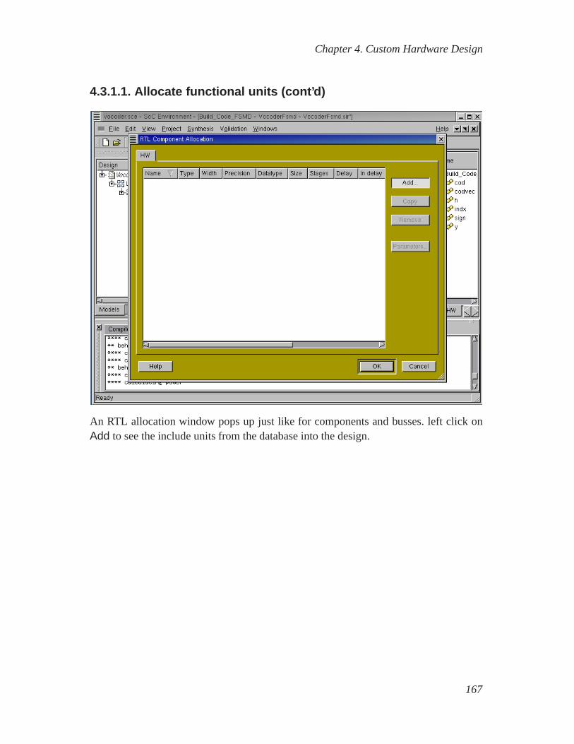
Chapter 4. Custom Hardware Design
4.3.1.1. Allocate functional units (cont’d)
An RTL allocation window pops up just like for components andbusses. left click onAdd to see the include units from the database into the design.
167
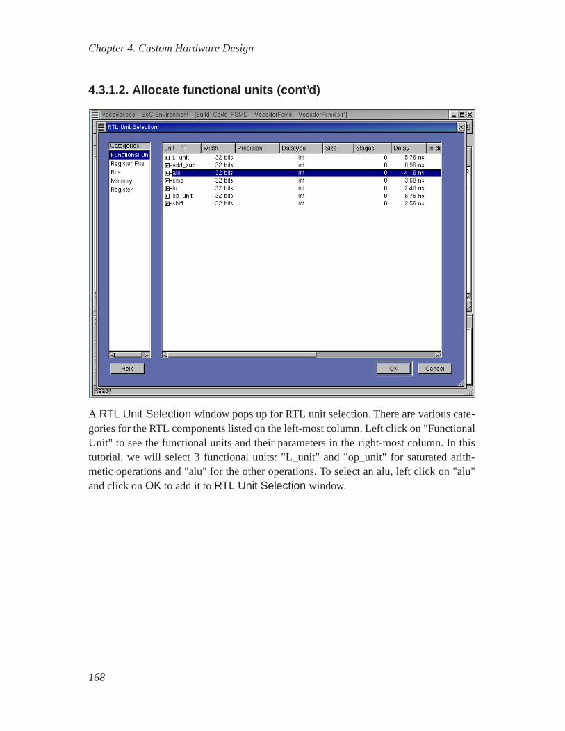
Chapter 4. Custom Hardware Design
4.3.1.2. Allocate functional units (cont’d)
A RTL Unit Selection window pops up for RTL unit selection. There are various cate-gories for the RTL components listed on the left-most column. Left click on "FunctionalUnit" to see the functional units and their parameters in theright-most column. In thistutorial, we will select 3 functional units: "L_unit" and "op_unit" for saturated arith-metic operations and "alu" for the other operations. To select an alu, left click on "alu"and click onOK to add it toRTL Unit Selection window.
168
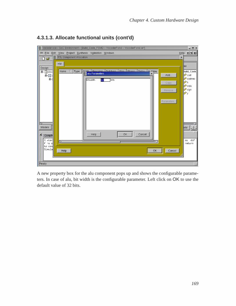
Chapter 4. Custom Hardware Design
4.3.1.3. Allocate functional units (cont’d)
A new property box for the alu component pops up and shows the configurable parame-ters. In case of alu, bit width is the configurable parameter.Left click on OK to use thedefault value of 32 bits.
169
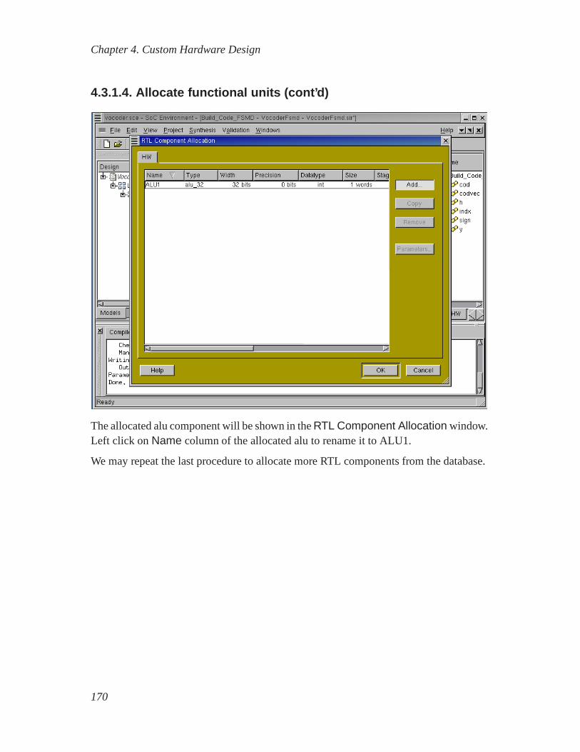
Chapter 4. Custom Hardware Design
4.3.1.4. Allocate functional units (cont’d)
The allocated alu component will be shown in theRTL Component Allocation window.Left click onName column of the allocated alu to rename it to ALU1.
We may repeat the last procedure to allocate more RTL components from the database.
170
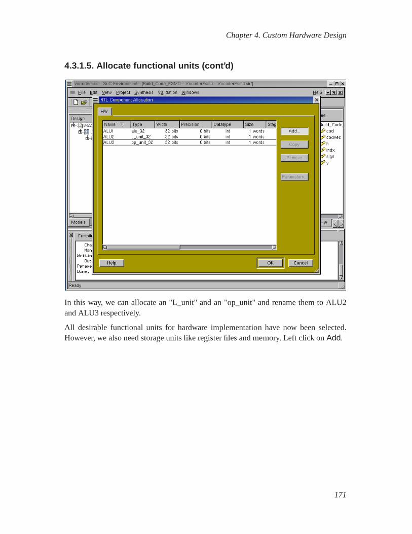
Chapter 4. Custom Hardware Design
4.3.1.5. Allocate functional units (cont’d)
In this way, we can allocate an "L_unit" and an "op_unit" and rename them to ALU2and ALU3 respectively.
All desirable functional units for hardware implementation have now been selected.However, we also need storage units like register files and memory. Left click onAdd.
171
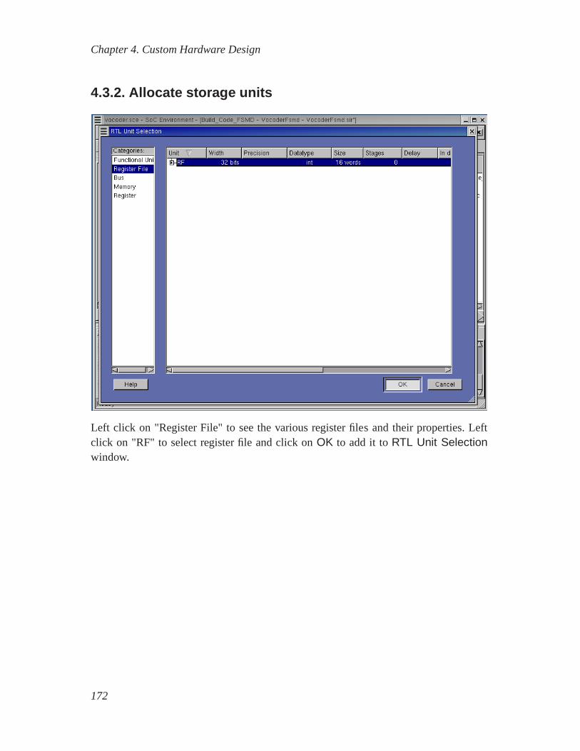
Chapter 4. Custom Hardware Design
4.3.2. Allocate storage units
Left click on "Register File" to see the various register files and their properties. Leftclick on "RF" to select register file and click onOK to add it toRTL Unit Selectionwindow.
172

Chapter 4. Custom Hardware Design
4.3.2.1. Allocate storage units (cont’d)
A new property box for RF component pops up and shows the configurable parame-ters. In case of RF, address width and size of register file as well as bit width are theconfigurable parameters. Left click on "Address width" to change 4 bits to 5 bits.
173
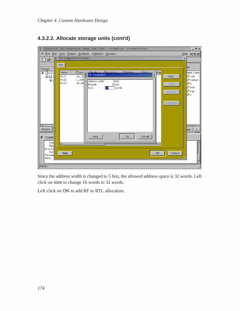
Chapter 4. Custom Hardware Design
4.3.2.2. Allocate storage units (cont’d)
Since the address width is changed to 5 bits, the allowed address space is 32 words. Leftclick onsize to change 16 words to 32 words.
Left click onOK to add RF to RTL allocation.
174

Chapter 4. Custom Hardware Design
4.3.2.3. Allocate storage units (cont’d)
The selected RF component will be shown in theRTL Component Allocation window.Left click onName column of the allocated RF to rename it to RF1.
175

Chapter 4. Custom Hardware Design
4.3.2.4. Allocate storage units (cont’d)
For the purpose of this design we will need 3 register files to perform RTL synthesis.To add more register files in the allocation table, simply Left click on Copy by 2 times.This is a useful way to replicate components for large sized allocations.
Now, we have allocated 3 register files. In the similar way, wecan allocate a memorycomponent.
176
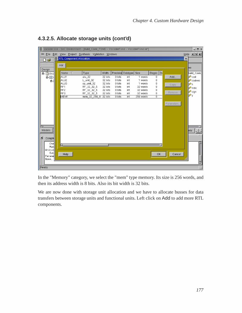
Chapter 4. Custom Hardware Design
4.3.2.5. Allocate storage units (cont’d)
In the "Memory" category, we select the "mem" type memory. Its size is 256 words, andthen its address width is 8 bits. Also its bit width is 32 bits.
We are now done with storage unit allocation and we have to allocate busses for datatransfers between storage units and functional units. Leftclick onAdd to add more RTLcomponents.
177

Chapter 4. Custom Hardware Design
4.3.3. Allocate buses
Left click on "Bus" to see its properties in the left-most column. Left click on "bus" toselect the bus and pressOK.
178

Chapter 4. Custom Hardware Design
4.3.3.1. Allocate buses (cont’d)
A new property box for bus component pops up and shows the configurable parameters.In case of bus, bit width is the configurable parameter. Left click on OK to add bus toRTL allocation.
179
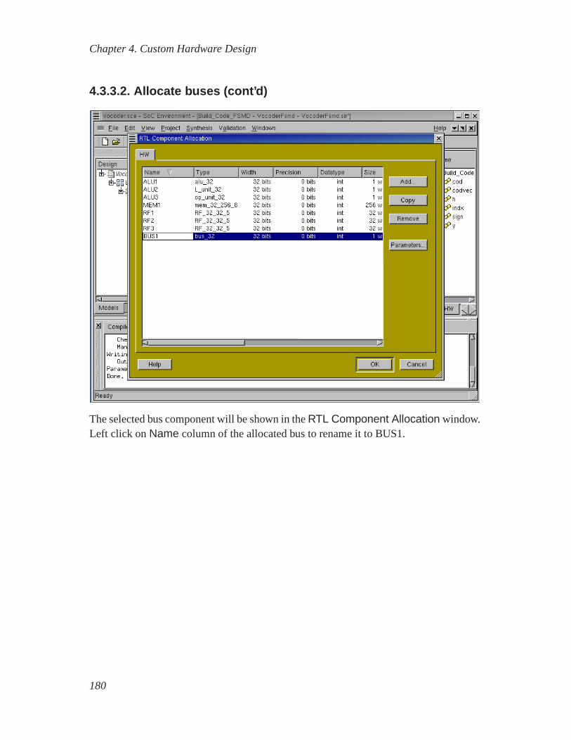
Chapter 4. Custom Hardware Design
4.3.3.2. Allocate buses (cont’d)
The selected bus component will be shown in theRTL Component Allocation window.Left click onName column of the allocated bus to rename it to BUS1.
180
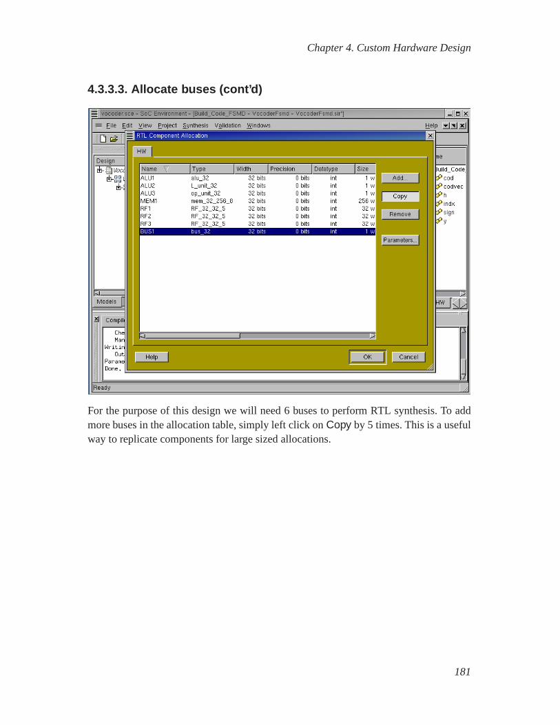
Chapter 4. Custom Hardware Design
4.3.3.3. Allocate buses (cont’d)
For the purpose of this design we will need 6 buses to perform RTL synthesis. To addmore buses in the allocation table, simply left click onCopy by 5 times. This is a usefulway to replicate components for large sized allocations.
181

Chapter 4. Custom Hardware Design
4.3.3.4. Allocate buses (cont’d)
We are now done with RTL component allocation. Left click onOK to save the alloca-tion information in the model.
182
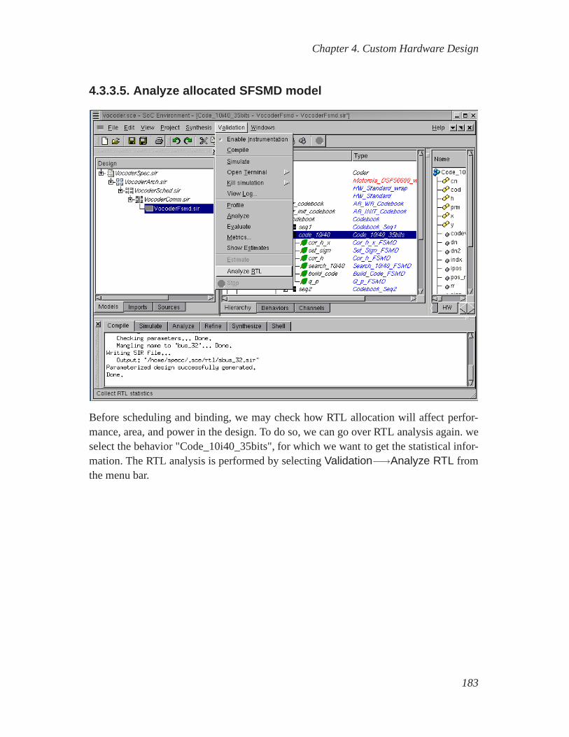
Chapter 4. Custom Hardware Design
4.3.3.5. Analyze allocated SFSMD model
Before scheduling and binding, we may check how RTL allocation will affect perfor-mance, area, and power in the design. To do so, we can go over RTL analysis again. weselect the behavior "Code_10i40_35bits", for which we wantto get the statistical infor-mation. The RTL analysis is performed by selectingValidation−→Analyze RTL fromthe menu bar.
183
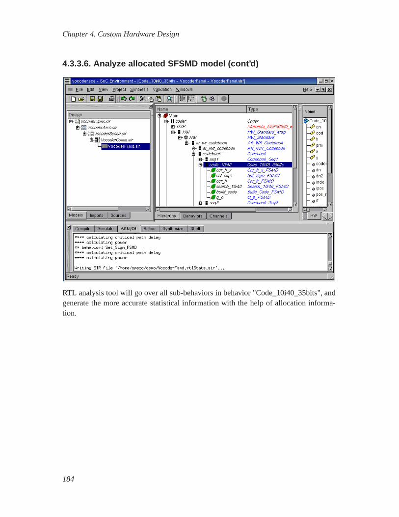
Chapter 4. Custom Hardware Design
4.3.3.6. Analyze allocated SFSMD model (cont’d)
RTL analysis tool will go over all sub-behaviors in behavior"Code_10i40_35bits", andgenerate the more accurate statistical information with the help of allocation informa-tion.
184

Chapter 4. Custom Hardware Design
4.3.3.7. Analyze allocated SFSMD model (cont’d)
Now, we will look at RTL analysis result because we allocatedRTL components for thedesign by selectingSynthesis−→Schedule & Bind RTL from the menu bar. Choosethe behavior "Build_Code_FSMD" from the hierarchy.
185
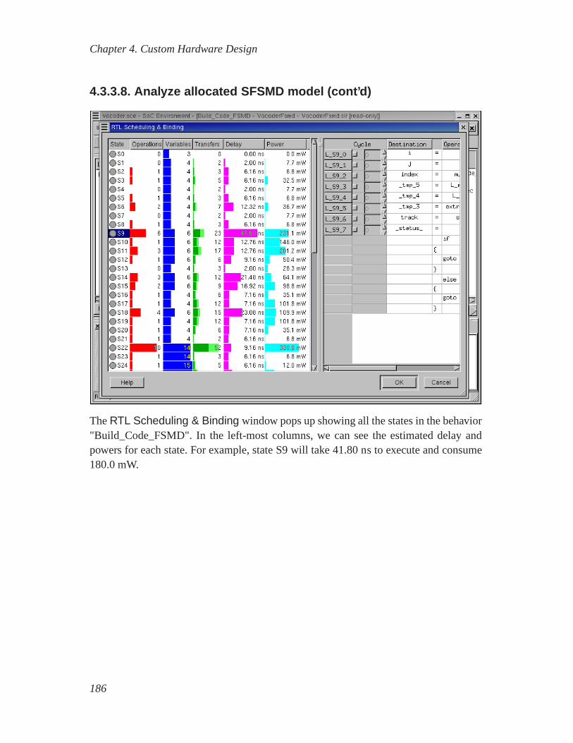
Chapter 4. Custom Hardware Design
4.3.3.8. Analyze allocated SFSMD model (cont’d)
TheRTL Scheduling & Binding window pops up showing all the states in the behavior"Build_Code_FSMD". In the left-most columns, we can see theestimated delay andpowers for each state. For example, state S9 will take 41.80 ns to execute and consume180.0 mW.
186
Chapter 4. Custom Hardware Design
4.4. RTL Scheduling and BindingThe most important steps during RTL synthesis are scheduling and binding. Schedulingis to decide the start time of operations in a design. Bindingis to map operations to func-tional units (function binding) and to map variables to storage units (storage binding),and to map data transfers to buses (connection binding). Dueto the interdependenceof scheduling and binding, the order of these steps may be interchanged to get betterdesign.
In our RTL design methodology, we provide manual schedulingand binding for the de-signers to make decision for scheduling and binding. But manual scheduling and bindingtakes too much time for the designers to do and is tedious and error-prone task. We willprovide automatic scheduling and binding tools by RTL plugins.
Note that if reader is not interested in how to do manual schedul-ing and binding, she or he can skip this section to go directlySection 4.4.2Schedule and bind automatically(page 200).
187

Chapter 4. Custom Hardware Design
4.4.1. Schedule and bind manually (optional)
SCE allows for the designer to manually schedule and bind theoperations. However,this is a tedious task and can be done by automated tools. To perform automaticscheduling and binding, the designer can skip the manual step and go directly toSection 4.4.2Schedule and bind automatically(page 200).
If RTL Scheduling & Binding window is not open yet, we have to open it again byselectingSynthesis−→Schedule & Bind RTL from the menu bar. Choose the behavior"Build_Code_FSMD" from the hierarchy.
we will show how to specify control step for each statement ina state. InRTL Schedul-ing and Binding window, we select "S9" to do manual scheduling and binding. In theright side panel of theRTL Scheduling & Binding window, left click on the right sideof the label "L_S9_0". This activates theCycle column for "L_S9_0". We can specifythe control step for it. In this way, we can specify control step for all statement in thestate S9.
Note that if reader is not interested in how to do manual schedul-
188

Chapter 4. Custom Hardware Design
ing and binding, she or he can skip this section to go directlySection 4.4.2Schedule and bind automatically(page 200).
189

Chapter 4. Custom Hardware Design
4.4.1.1. Schedule and bind manually (optional) (cont’d)
To perform manual binding for operations in the state S9, right click on Label, "L_S9_2".It will pop up a menu for the binding options. SelectFull binding.
190

Chapter 4. Custom Hardware Design
4.4.1.2. Schedule and bind manually (optional) (cont’d)
Each column in a statement in right side of the window is now expanded to allow manualbinding. We will bind a function call, mult (Operation column), to "ALU3". To do so,left click on 2nd blank row of theOperation column. Then pull-down menu pops upand shows all functional units which can perform function call mult. In this case, onepossible functional unit, "ALU3" is shown in the pull-down menu.
191

Chapter 4. Custom Hardware Design
4.4.1.3. Schedule and bind manually (optional) (cont’d)
We will bind a target variable index (Destination column) to RF1[7]. To do so, left clickon 2nd blank row of theDestination column. Then pull-down menu pops up and showsall storage units In this case, four storage units such as "MEM1", "RF1", "RF2" and"RF3" are shown in the pull-down menu. Click on "RF1" to select "RF1".
192

Chapter 4. Custom Hardware Design
4.4.1.4. Schedule and bind manually (optional) (cont’d)
For storage unit binding, the address of the variable in the memory should be specified.Left click on right side of the 2nd row ofDestination column. Specify the memoryaddress to 7 for variable "index". The -1 in address field for amemory is default valuewhich means that the address for the memory is not bound yet.
193

Chapter 4. Custom Hardware Design
4.4.1.5. Schedule and bind manually (optional) (cont’d)
Likewise, source variable, "i" is bound to RF2[3].
194
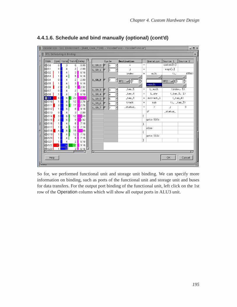
Chapter 4. Custom Hardware Design
4.4.1.6. Schedule and bind manually (optional) (cont’d)
So for, we performed functional unit and storage unit binding. We can specify moreinformation on binding, such as ports of the functional unitand storage unit and busesfor data transfers. For the output port binding of the functional unit, left click on the 1strow of theOperation column which will show all output ports in ALU3 unit.
195
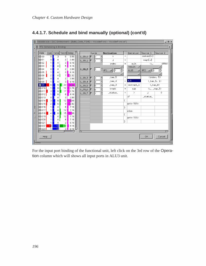
Chapter 4. Custom Hardware Design
4.4.1.7. Schedule and bind manually (optional) (cont’d)
For the input port binding of the functional unit, left clickon the 3rd row of theOpera-tion column which will shows all input ports in ALU3 unit.
196
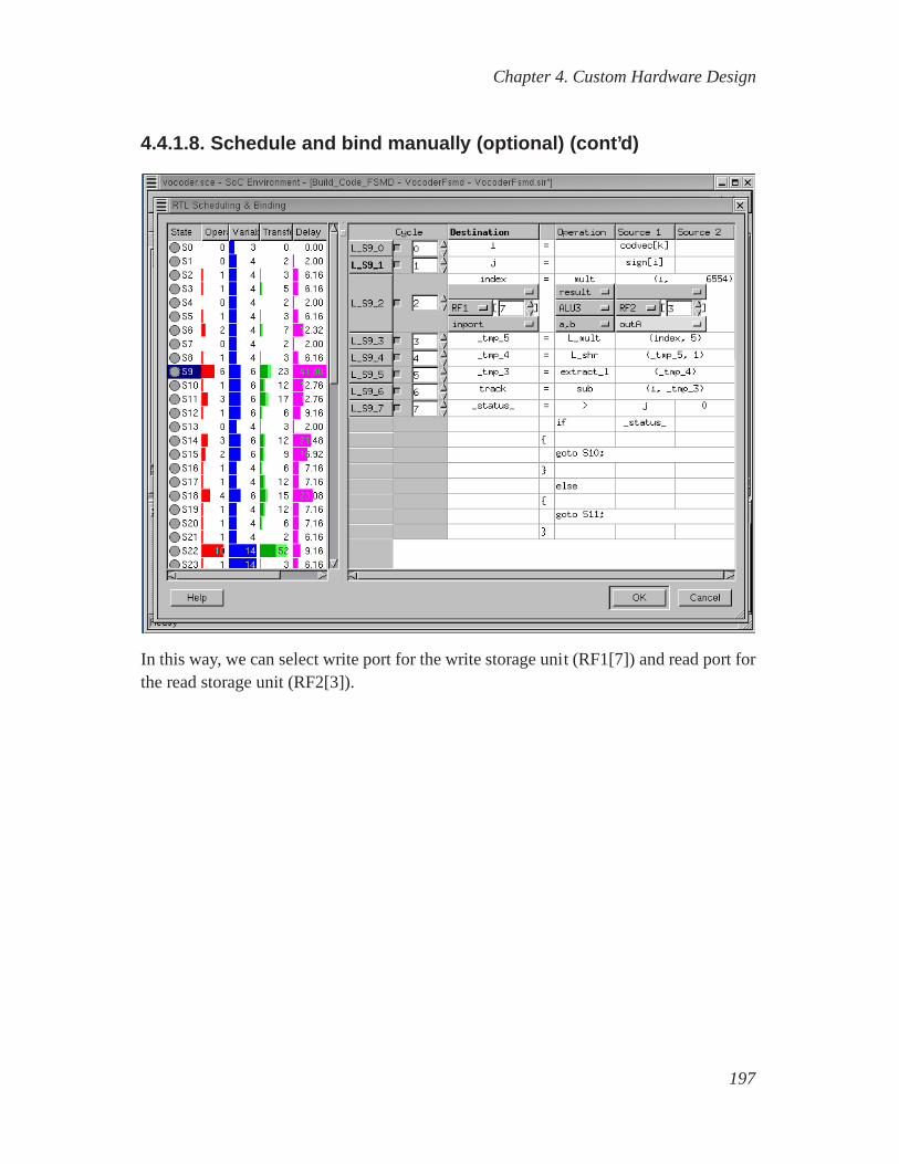
Chapter 4. Custom Hardware Design
4.4.1.8. Schedule and bind manually (optional) (cont’d)
In this way, we can select write port for the write storage unit (RF1[7]) and read port forthe read storage unit (RF2[3]).
197

Chapter 4. Custom Hardware Design
4.4.1.9. Schedule and bind manually (optional) (cont’d)
For the bus binding, left click on the 1st row of theDestination column which showsall allocated buses. For target variable "index", "BUS3" isselected for write.
198
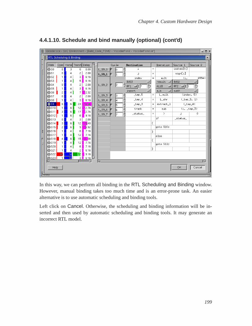
Chapter 4. Custom Hardware Design
4.4.1.10. Schedule and bind manually (optional) (cont’d)
In this way, we can perform all binding in theRTL Scheduling and Binding window.However, manual binding takes too much time and is an error-prone task. An easieralternative is to use automatic scheduling and binding tools.
Left click on Cancel. Otherwise, the scheduling and binding information will bein-serted and then used by automatic scheduling and binding tools. It may generate anincorrect RTL model.
199

Chapter 4. Custom Hardware Design
4.4.2. Schedule and bind automatically
As already discussed, manual scheduling and binding takes too much time for a designerto do and also is an error-prone task. We will now perform scheduling and binding withthe help of tools which implement scheduling and binding algorithms. In our designflow, an automatic decision making tool for system-level design is called a "Plug in". ForRTL scheduling and binding, we call "RTL Plugins" by selecting Synthesis−→RTLPlugIns−→scrtl_bind from the menu bar. Before that, we have to select a behavior"Code_10i40_35bits".
200
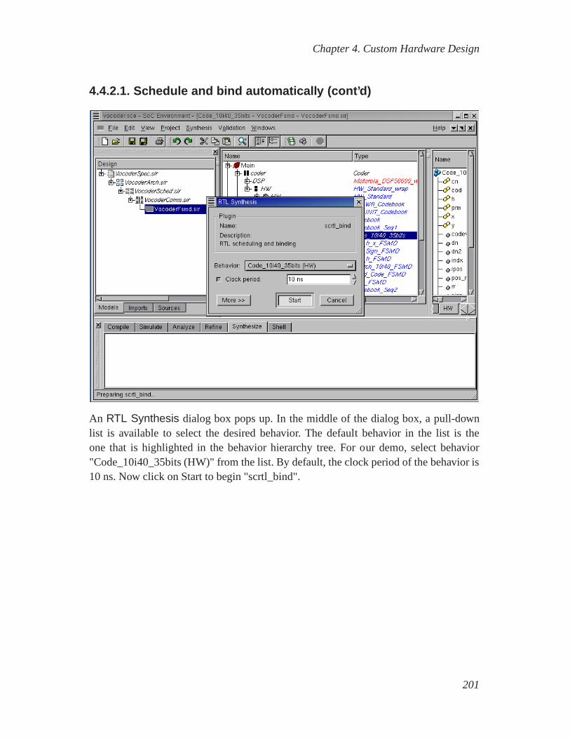
Chapter 4. Custom Hardware Design
4.4.2.1. Schedule and bind automatically (cont’d)
An RTL Synthesis dialog box pops up. In the middle of the dialog box, a pull-downlist is available to select the desired behavior. The default behavior in the list is theone that is highlighted in the behavior hierarchy tree. For our demo, select behavior"Code_10i40_35bits (HW)" from the list. By default, the clock period of the behavior is10 ns. Now click on Start to begin "scrtl_bind".
201

Chapter 4. Custom Hardware Design
4.4.2.2. Schedule and bind automatically (cont’d)
Note that "scrtl_bind" annotates scheduling and binding information into SFSMDs forall 6 sub-behaviors of the behavior "Code_10i40_35bits", as seen in the logging window.The tool finally generates the SFSMD model for the behavior "Code_10i40_35bits".
202
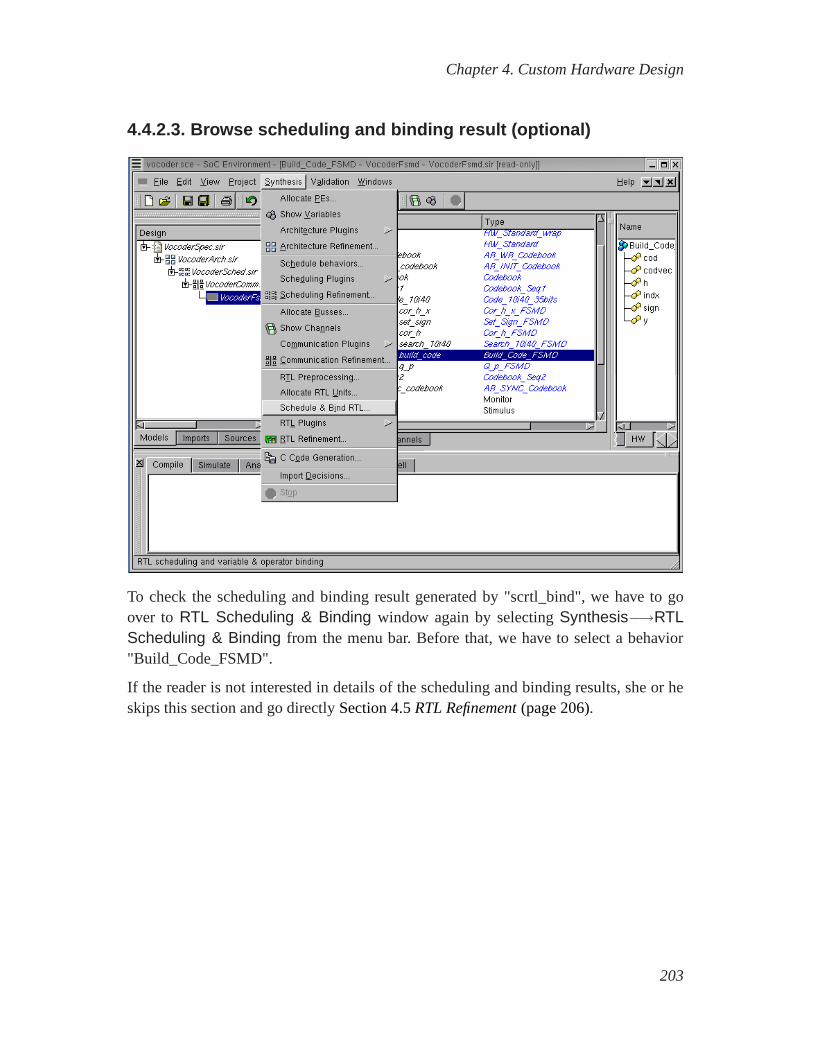
Chapter 4. Custom Hardware Design
4.4.2.3. Browse scheduling and binding result (optional)
To check the scheduling and binding result generated by "scrtl_bind", we have to goover to RTL Scheduling & Binding window again by selectingSynthesis−→RTLScheduling & Binding from the menu bar. Before that, we have to select a behavior"Build_Code_FSMD".
If the reader is not interested in details of the scheduling and binding results, she or heskips this section and go directlySection 4.5RTL Refinement(page 206).
203
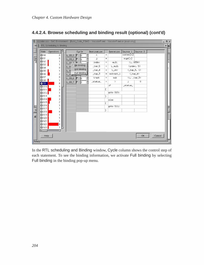
Chapter 4. Custom Hardware Design
4.4.2.4. Browse scheduling and binding result (optional) ( cont’d)
In theRTL scheduling and Binding window,Cycle column shows the control step ofeach statement. To see the binding information, we activateFull binding by selectingFull binding in the binding pop-up menu.
204
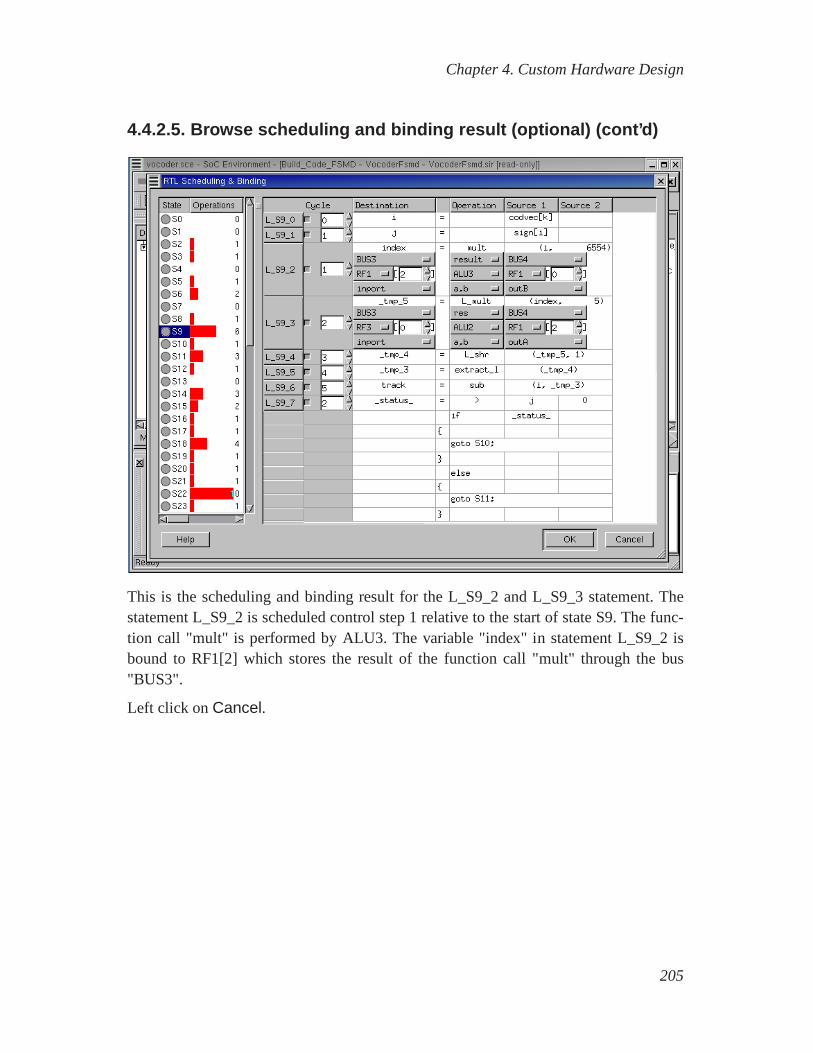
Chapter 4. Custom Hardware Design
4.4.2.5. Browse scheduling and binding result (optional) ( cont’d)
This is the scheduling and binding result for the L_S9_2 and L_S9_3 statement. Thestatement L_S9_2 is scheduled control step 1 relative to thestart of state S9. The func-tion call "mult" is performed by ALU3. The variable "index" in statement L_S9_2 isbound to RF1[2] which stores the result of the function call "mult" through the bus"BUS3".
Left click onCancel.
205
Chapter 4. Custom Hardware Design
4.5. RTL RefinementSo far, we performed allocation, scheduling and binding of which information is an-notated into the SFSMD model. Then the SFSMD model should be refined into cycle-accurate RTL model, which is represented by finite state machine with data (FSMD).The cycle-accurate model will reflect all scheduling and binding information.
Basically, this step will split the state to the multiple states reflecting scheduling infor-mation. Now each state will take exactly one clock period to perform.
The RTL refinement tool can generate cycle-accurate FSMD models in various hardwaredescription languages such as Verilog HDL and Handel-C in addition to SpecC. TheVerilog HDL model will be used as input for commercial logic synthesis tool like DesignCompiler from Synopsys. Also the Handel-C model will be fed into Celoxica Design Kitto generate gate-level netlist.
206
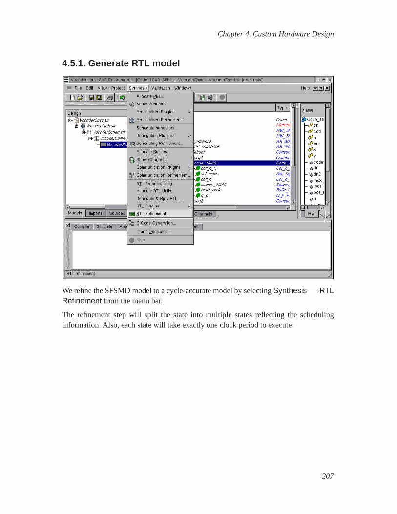
Chapter 4. Custom Hardware Design
4.5.1. Generate RTL model
We refine the SFSMD model to a cycle-accurate model by selectingSynthesis−→RTLRefinement from the menu bar.
The refinement step will split the state into multiple statesreflecting the schedulinginformation. Also, each state will take exactly one clock period to execute.
207
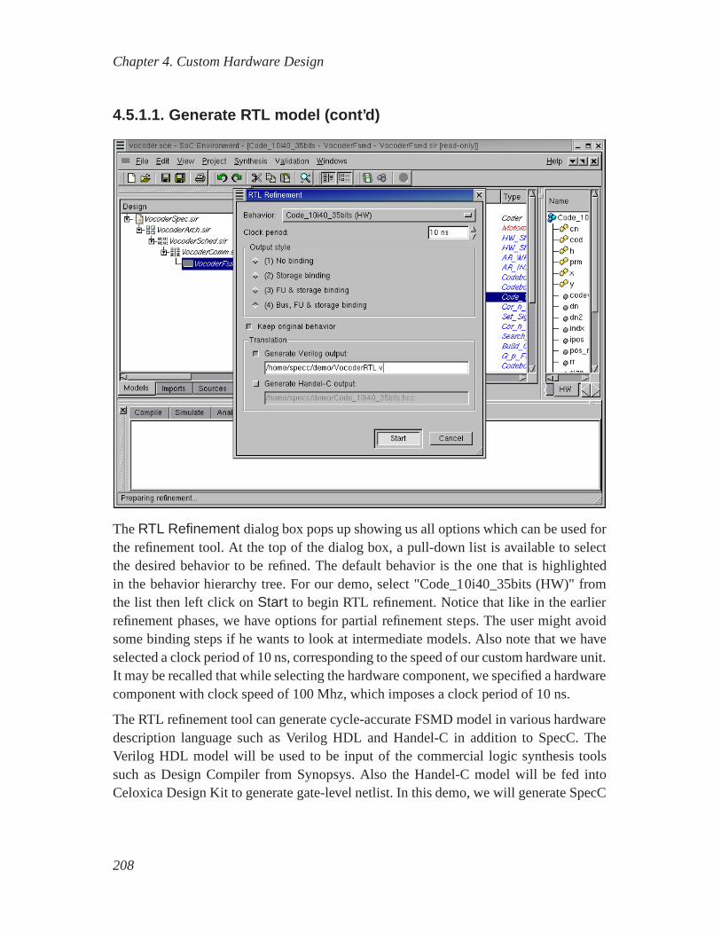
Chapter 4. Custom Hardware Design
4.5.1.1. Generate RTL model (cont’d)
TheRTL Refinement dialog box pops up showing us all options which can be used forthe refinement tool. At the top of the dialog box, a pull-down list is available to selectthe desired behavior to be refined. The default behavior is the one that is highlightedin the behavior hierarchy tree. For our demo, select "Code_10i40_35bits (HW)" fromthe list then left click onStart to begin RTL refinement. Notice that like in the earlierrefinement phases, we have options for partial refinement steps. The user might avoidsome binding steps if he wants to look at intermediate models. Also note that we haveselected a clock period of 10 ns, corresponding to the speed of our custom hardware unit.It may be recalled that while selecting the hardware component, we specified a hardwarecomponent with clock speed of 100 Mhz, which imposes a clock period of 10 ns.
The RTL refinement tool can generate cycle-accurate FSMD model in various hardwaredescription language such as Verilog HDL and Handel-C in addition to SpecC. TheVerilog HDL model will be used to be input of the commercial logic synthesis toolssuch as Design Compiler from Synopsys. Also the Handel-C model will be fed intoCeloxica Design Kit to generate gate-level netlist. In thisdemo, we will generate SpecC
208

Chapter 4. Custom Hardware Design
RTL and Verilog HDL model for the design.
Change the output file name for the Verilog HDL model to "VocoderRTL.v".
209

Chapter 4. Custom Hardware Design
4.5.1.2. Generate RTL model (cont’d)
Note that the RTL refinement step generates a new RTL model for6 sub-behaviors ofthe behavior "Code_10i40_35bits", as seen in the logging window. Also note that a newmodel "VocoderFsmd.rtl.sir" is added in the Project manager window.
210
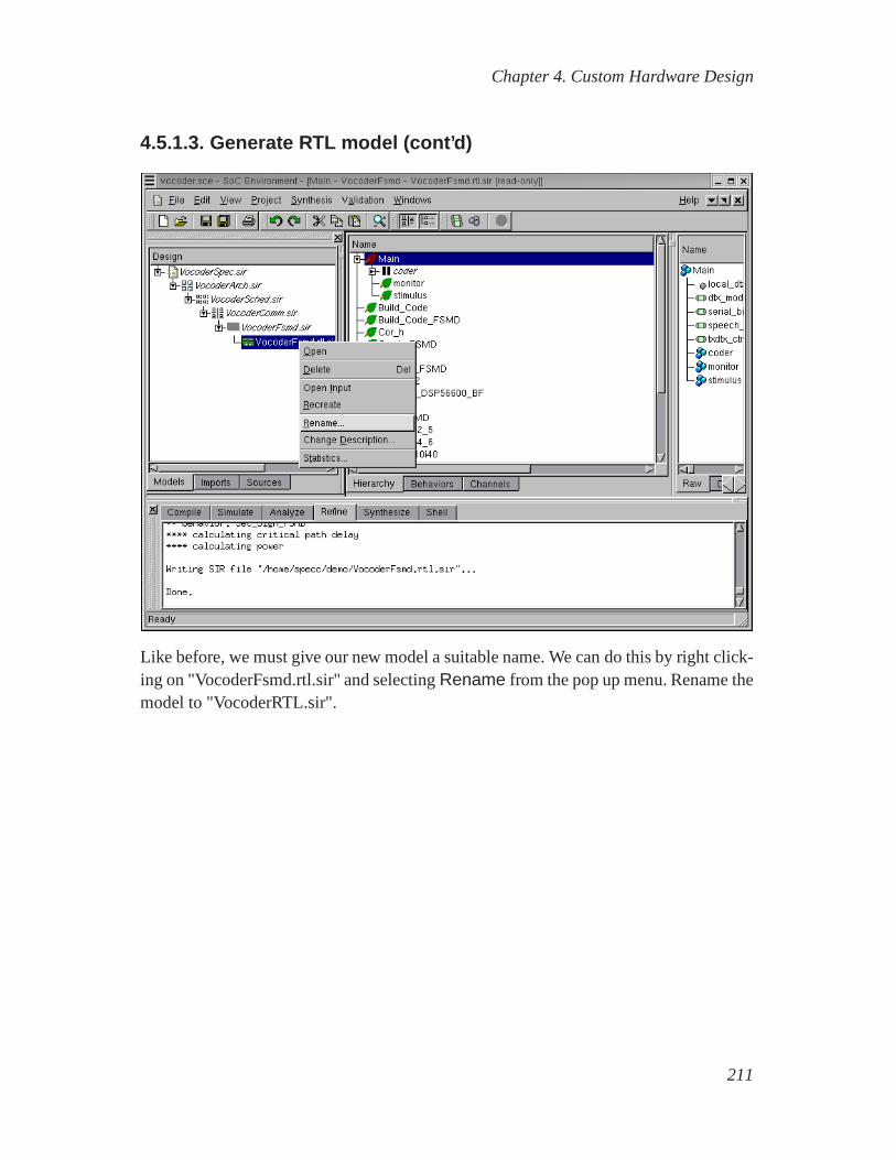
Chapter 4. Custom Hardware Design
4.5.1.3. Generate RTL model (cont’d)
Like before, we must give our new model a suitable name. We cando this by right click-ing on "VocoderFsmd.rtl.sir" and selectingRename from the pop up menu. Rename themodel to "VocoderRTL.sir".
211
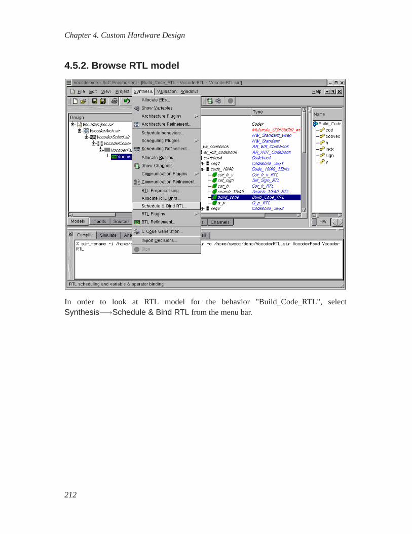
Chapter 4. Custom Hardware Design
4.5.2. Browse RTL model
In order to look at RTL model for the behavior "Build_Code_RTL", selectSynthesis−→Schedule & Bind RTL from the menu bar.
212
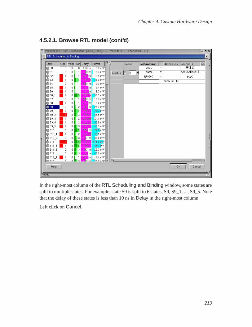
Chapter 4. Custom Hardware Design
4.5.2.1. Browse RTL model (cont’d)
In the right-most column of theRTL Scheduling and Binding window, some states aresplit to multiple states. For example, state S9 is split to 6 states, S9, S9_1, ..., S9_5. Notethat the delay of these states is less than 10 ns inDelay in the right-most column.
Left click onCancel.
213

Chapter 4. Custom Hardware Design
4.5.3. View RTL model (optional)
We now browse through the newly created model in the Design hierarchy window. Notethat the type of the instance "build_code" has now changed to"Build_Code_RTL" afterRTL refinement.
Select the behavior "Build_Code_RTL" by left clicking on it. We now take a look at thesynthesized source code to see if the RTL refinement tool has correctly generated theRTL model. Do this by selectingView−→Source from the menu bar.
If the reader is not interested, he or she may skip this section to go directly toSection 4.5.4View Verilog RTL model (optional)(page 217).
214
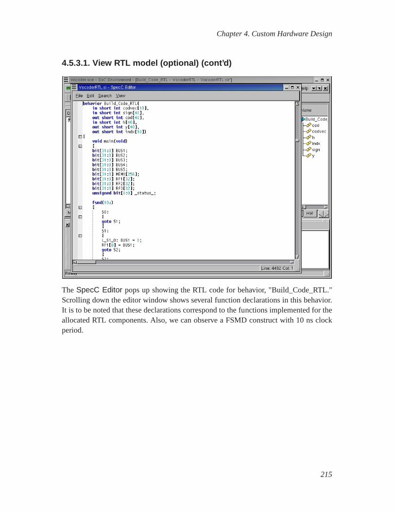
Chapter 4. Custom Hardware Design
4.5.3.1. View RTL model (optional) (cont’d)
The SpecC Editor pops up showing the RTL code for behavior, "Build_Code_RTL."Scrolling down the editor window shows several function declarations in this behavior.It is to be noted that these declarations correspond to the functions implemented for theallocated RTL components. Also, we can observe a FSMD construct with 10 ns clockperiod.
215
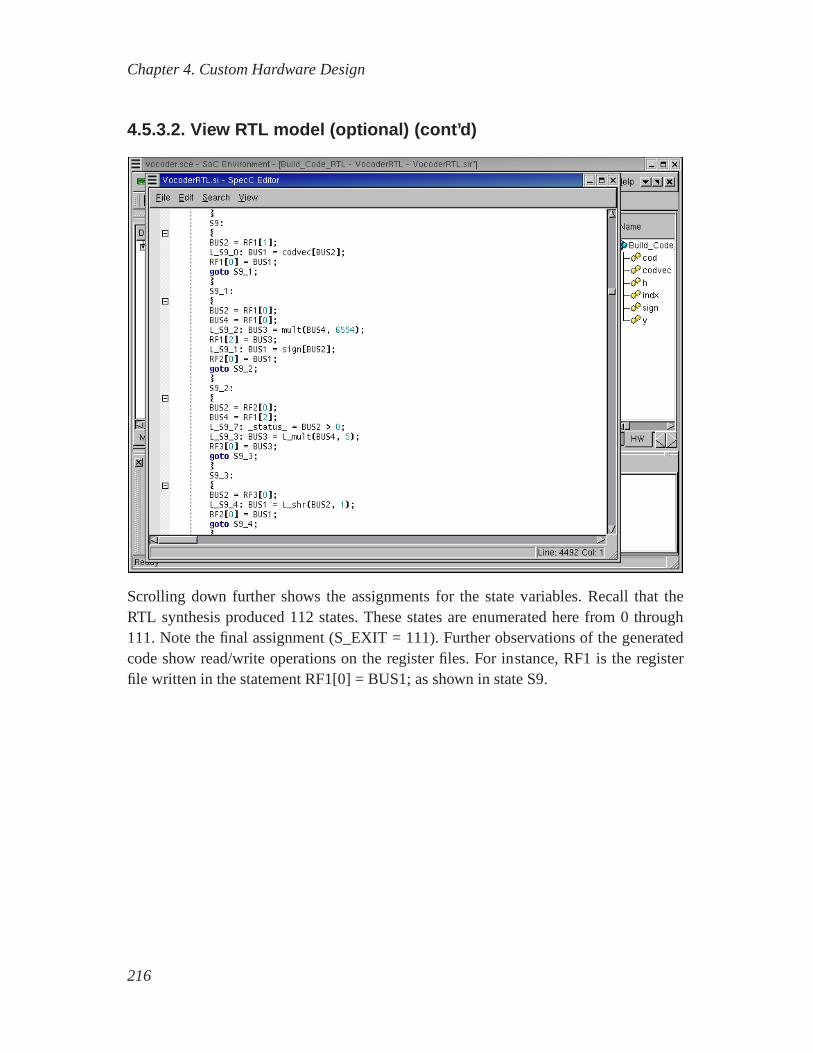
Chapter 4. Custom Hardware Design
4.5.3.2. View RTL model (optional) (cont’d)
Scrolling down further shows the assignments for the state variables. Recall that theRTL synthesis produced 112 states. These states are enumerated here from 0 through111. Note the final assignment (S_EXIT = 111). Further observations of the generatedcode show read/write operations on the register files. For instance, RF1 is the registerfile written in the statement RF1[0] = BUS1; as shown in state S9.
216
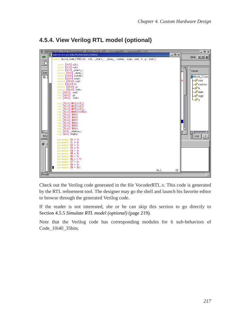
Chapter 4. Custom Hardware Design
4.5.4. View Verilog RTL model (optional)
Check out the Verilog code generated in the file VocoderRTL.v. This code is generatedby the RTL refinement tool. The designer may go the shell and launch his favorite editorto browse through the generated Verilog code.
If the reader is not interested, she or he can skip this section to go directly toSection 4.5.5Simulate RTL model (optional)(page 219).
Note that the Verilog code has corresponding modules for 6 sub-behaviors ofCode_10i40_35bits.
217
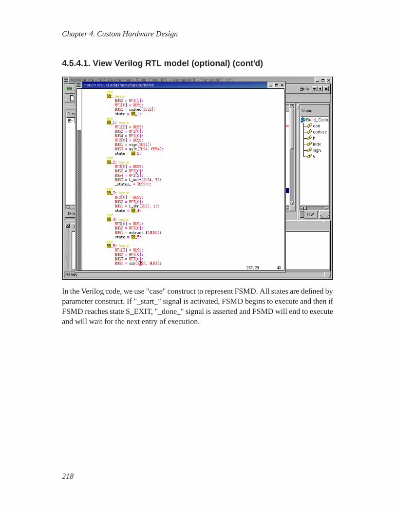
Chapter 4. Custom Hardware Design
4.5.4.1. View Verilog RTL model (optional) (cont’d)
In the Verilog code, we use "case" construct to represent FSMD. All states are defined byparameter construct. If "_start_" signal is activated, FSMD begins to execute and then ifFSMD reaches state S_EXIT, "_done_" signal is asserted and FSMD will end to executeand will wait for the next entry of execution.
218

Chapter 4. Custom Hardware Design
4.5.5. Simulate RTL model (optional)
Now, we have to create an executable for the generated FSMD model by selectingValidation−→Compile from the menu bar.
If reader is not interested, she or he can skip this section togo directlyChapter 5Embedded Software Design(page 223).
219
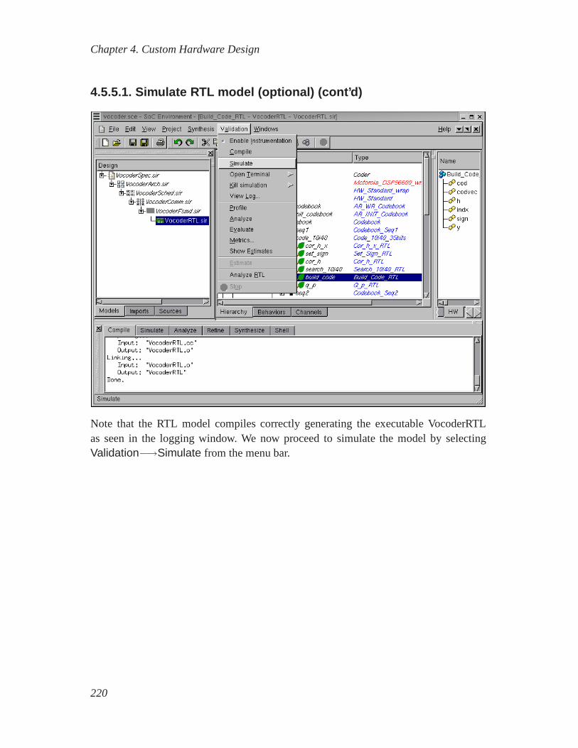
Chapter 4. Custom Hardware Design
4.5.5.1. Simulate RTL model (optional) (cont’d)
Note that the RTL model compiles correctly generating the executable VocoderRTLas seen in the logging window. We now proceed to simulate the model by selectingValidation−→Simulate from the menu bar.
220
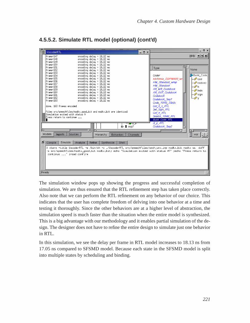
Chapter 4. Custom Hardware Design
4.5.5.2. Simulate RTL model (optional) (cont’d)
The simulation window pops up showing the progress and successful completion ofsimulation. We are thus ensured that the RTL refinement step has taken place correctly.Also note that we can perform the RTL refinement on any behavior of our choice. Thisindicates that the user has complete freedom of delving intoone behavior at a time andtesting it thoroughly. Since the other behaviors are at a higher level of abstraction, thesimulation speed is much faster than the situation when the entire model is synthesized.This is a big advantage with our methodology and it enables partial simulation of the de-sign. The designer does not have to refine the entire design tosimulate just one behaviorin RTL.
In this simulation, we see the delay per frame in RTL model increases to 18.13 ns from17.05 ns compared to SFSMD model. Because each state in the SFSMD model is splitinto multiple states by scheduling and binding.
221
Chapter 4. Custom Hardware Design
4.6. SummaryIn this chapter we showed the task of custom HW design for the behaviors mapped toHW component. We started from a bus functional model of the system and isolated thebehaviors that we want to implement in HW. These behaviors underwent a series oftransformations to arrive at a FSMD style model that can serve as input to industry stan-dard logic synthesis tools. Besides, generating the SpecC models, SCE is also capable ofgenerating HW models in standard HDL like Verilog and Handel-C, which can be usedby the Celoxica Design Kit.
We also saw various advantages of working with SCE during RTLsynthesis. The envi-ronment and language allow the user to concentrate only on one behavior if he or sheneeds to. That is, the designer may choose to perform cycle a accurate implementationof a critical behavior and keep the remaining behaviors at a higher level of abstractionfor fast simulation. The RTL synthesis process itself allows the designer to perform thescheduling and binding steps manually. However, we also showed the automatic RTLsynthesis capabilities. The designer is free to tweak the synthesis results and generate anew model at any time.
222
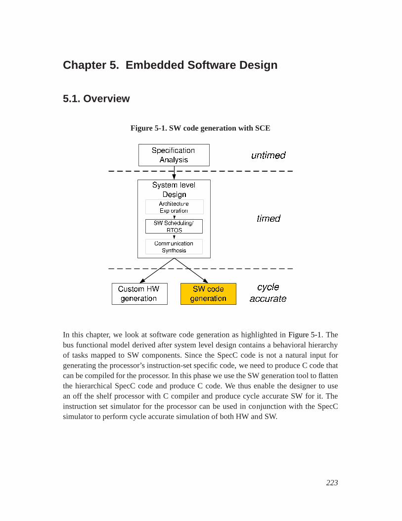
Chapter 5. Embedded Software Design
5.1. Overview
Figure 5-1. SW code generation with SCE
In this chapter, we look at software code generation as highlighted inFigure 5-1. Thebus functional model derived after system level design contains a behavioral hierarchyof tasks mapped to SW components. Since the SpecC code is not anatural input forgenerating the processor’s instruction-set specific code,we need to produce C code thatcan be compiled for the processor. In this phase we use the SW generation tool to flattenthe hierarchical SpecC code and produce C code. We thus enable the designer to usean off the shelf processor with C compiler and produce cycle accurate SW for it. Theinstruction set simulator for the processor can be used in conjunction with the SpecCsimulator to perform cycle accurate simulation of both HW and SW.
223
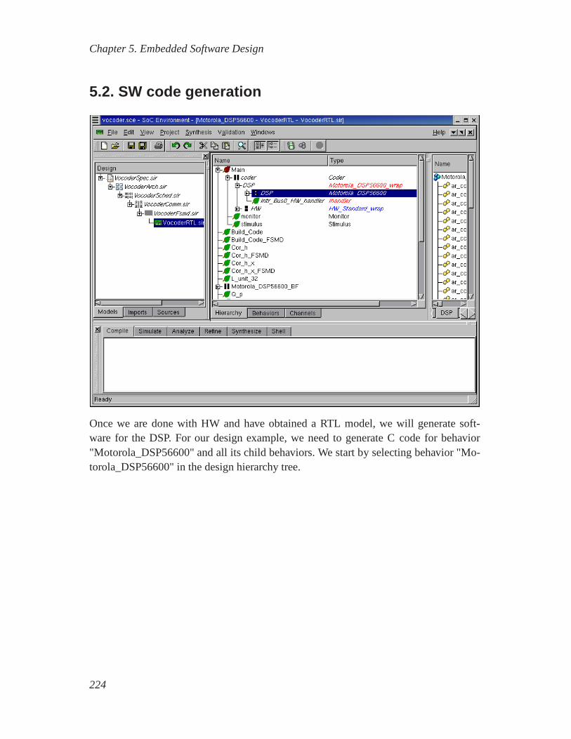
Chapter 5. Embedded Software Design
5.2. SW code generation
Once we are done with HW and have obtained a RTL model, we will generate soft-ware for the DSP. For our design example, we need to generate Ccode for behavior"Motorola_DSP56600" and all its child behaviors. We start by selecting behavior "Mo-torola_DSP56600" in the design hierarchy tree.
224
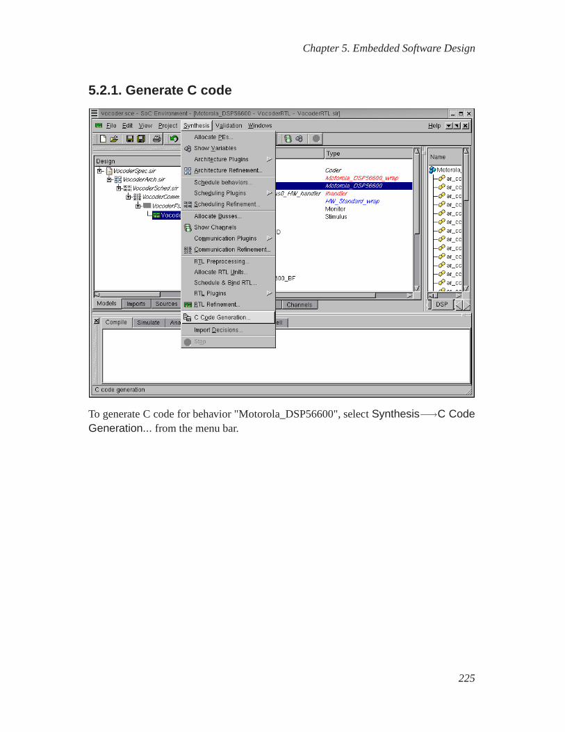
Chapter 5. Embedded Software Design
5.2.1. Generate C code
To generate C code for behavior "Motorola_DSP56600", select Synthesis−→C CodeGeneration... from the menu bar.
225

Chapter 5. Embedded Software Design
5.2.1.1. Generate C code (cont’d)
A dialog box pops up for the user to input the name of the C and Header file of thegenerated software. Now press theStart button to start the C code generation process.
226
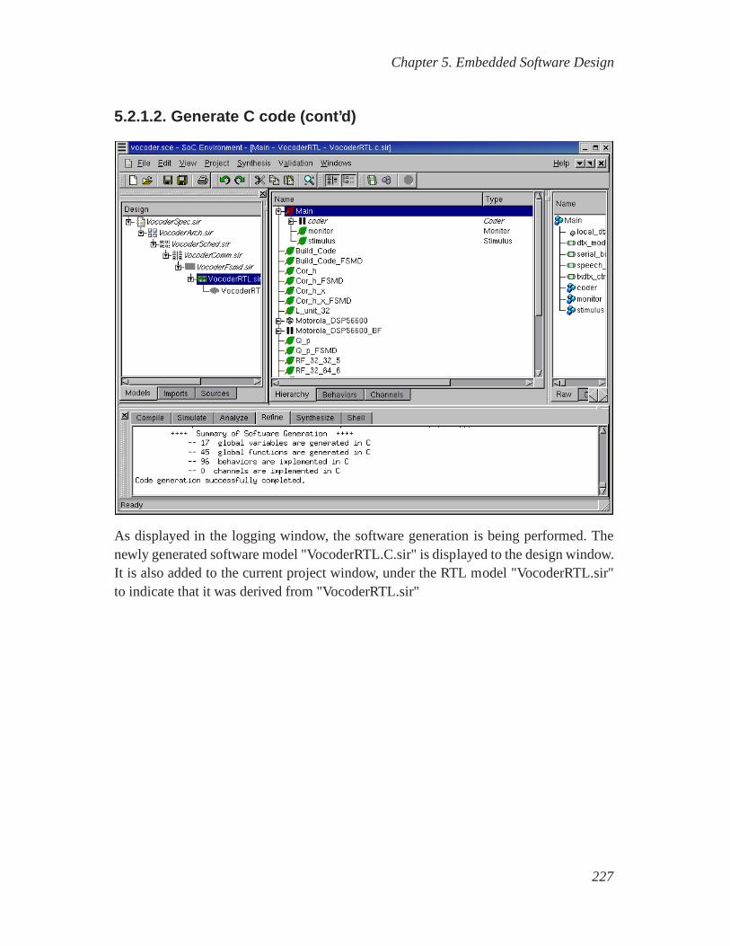
Chapter 5. Embedded Software Design
5.2.1.2. Generate C code (cont’d)
As displayed in the logging window, the software generationis being performed. Thenewly generated software model "VocoderRTL.C.sir" is displayed to the design window.It is also added to the current project window, under the RTL model "VocoderRTL.sir"to indicate that it was derived from "VocoderRTL.sir"
227
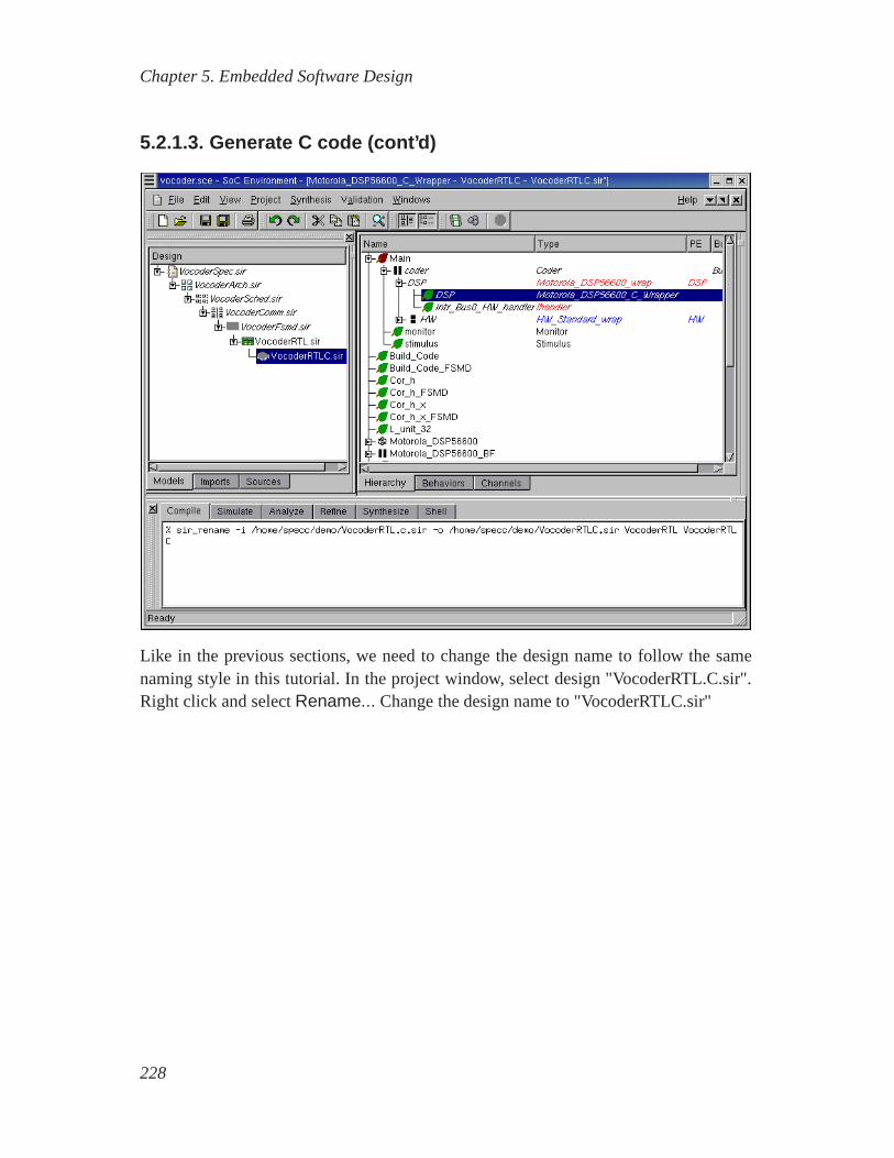
Chapter 5. Embedded Software Design
5.2.1.3. Generate C code (cont’d)
Like in the previous sections, we need to change the design name to follow the samenaming style in this tutorial. In the project window, selectdesign "VocoderRTL.C.sir".Right click and selectRename... Change the design name to "VocoderRTLC.sir"
228

Chapter 5. Embedded Software Design
5.2.2. Browse and View C code
Check out the C code generated in the file "Motorola_DSP56600.c". This code is gen-erated by the software generation tool. The designer may go to the shell and launch hisfavorite editor to browse through the generated C code.
The code generation process converts the SpecC descriptionof tasks into ANSI C code.The main idea is that we convert the behaviors and channels into C struct and convertthe behavioral hierarchy into the C struct hierarchy. Variables defined inside a behavioror channel and ports of behaviors are converted into data members of the correspondingC struct. Finally, functions inside a behavior or channel are converted into global func-tions with an additional parameter added representing the behavior to which the functionbelongs.
229

Chapter 5. Embedded Software Design
5.2.3. Simulate C model (optional)
So far we have finished the C code generation. However, we alsoneed to confirmthat the generated C code is correct for the design. In other words the C code mustbe functionally equivalent to the SpecC model. The simulation step is optional,so if the designer is not interested in it, he or she may skip itand go directly toSection 5.3Instruction set simulation(page 233).
We will validate the generated C code through simulation. But first we need to import Ccode into the design and compile the model into an executable. To compile the C codemodel to executable, go toValidation menu and selectCompile .
230

Chapter 5. Embedded Software Design
5.2.3.1. Simulate C model (cont’d)
The messages in the logging window shows that the C code modelis compiled success-fully without any syntax errors. Now in order to verify that it is functionally equivalentto the previous model, we will simulate the compiled model onthe same set of speechdata used in the specification validation. Go toValidation menu and selectSimulate .
231
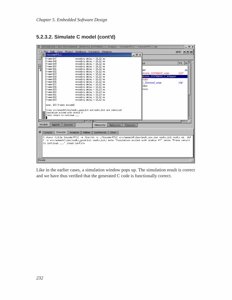
Chapter 5. Embedded Software Design
5.2.3.2. Simulate C model (cont’d)
Like in the earlier cases, a simulation window pops up. The simulation result is correctand we have thus verified that the generated C code is functionally correct.
232
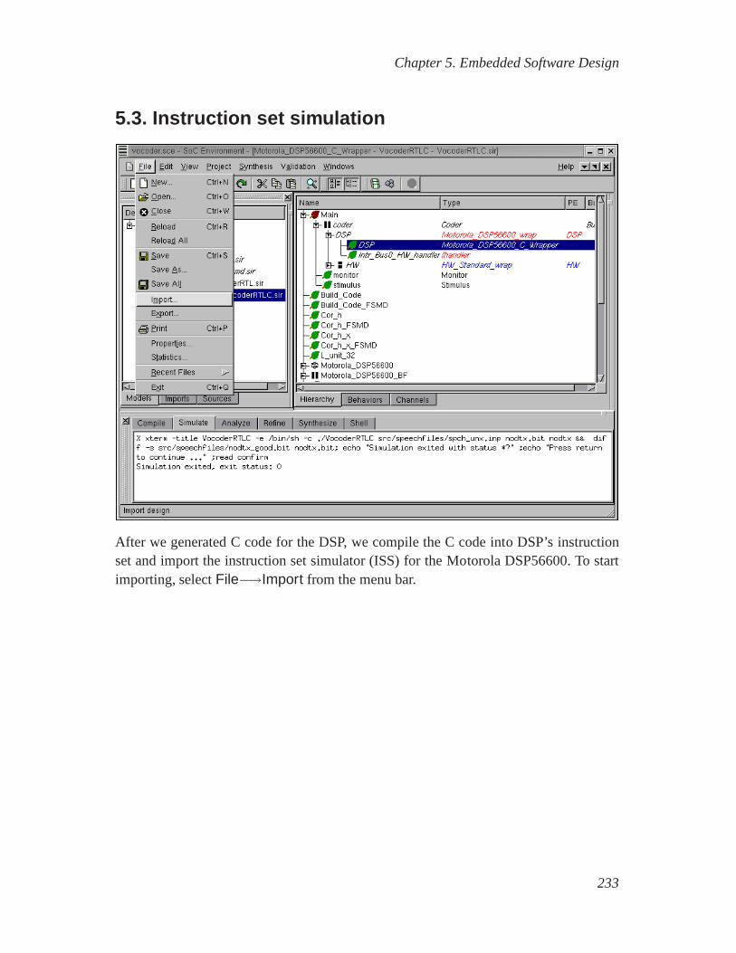
Chapter 5. Embedded Software Design
5.3. Instruction set simulation
After we generated C code for the DSP, we compile the C code into DSP’s instructionset and import the instruction set simulator (ISS) for the Motorola DSP56600. To startimporting, selectFile−→Import from the menu bar.
233
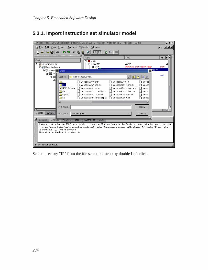
Chapter 5. Embedded Software Design
5.3.1. Import instruction set simulator model
Select directory "IP" from the file selection menu by double Left click.
234
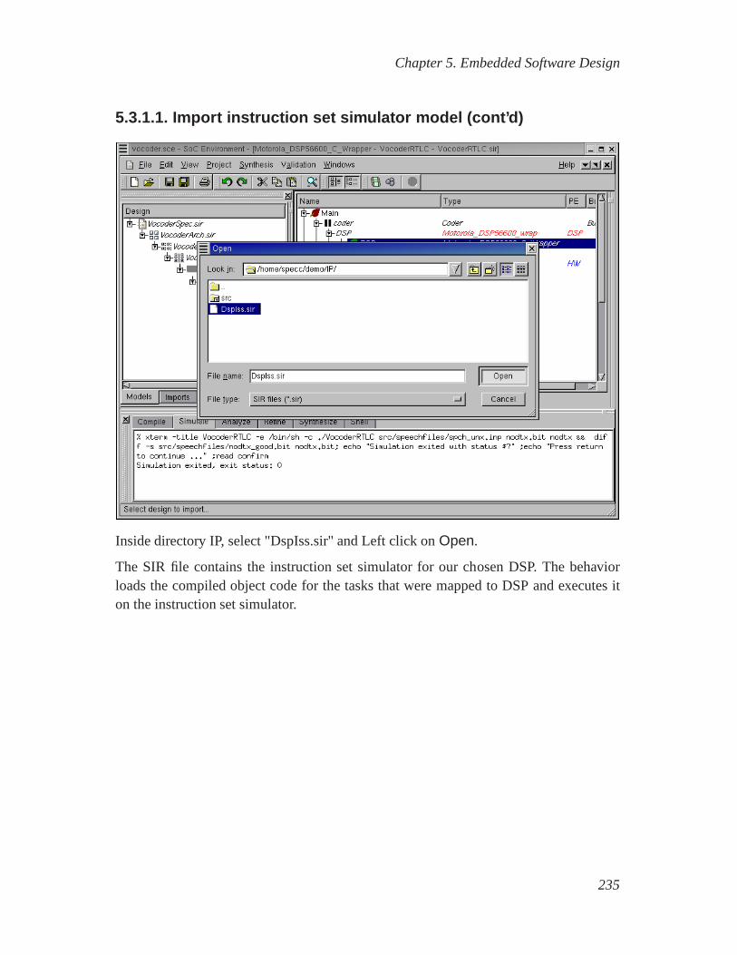
Chapter 5. Embedded Software Design
5.3.1.1. Import instruction set simulator model (cont’d)
Inside directory IP, select "DspIss.sir" and Left click onOpen.
The SIR file contains the instruction set simulator for our chosen DSP. The behaviorloads the compiled object code for the tasks that were mappedto DSP and executes iton the instruction set simulator.
235
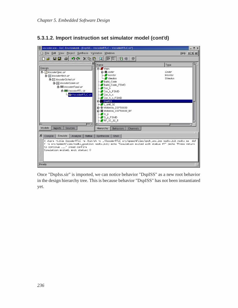
Chapter 5. Embedded Software Design
5.3.1.2. Import instruction set simulator model (cont’d)
Once "DspIss.sir" is imported, we can notice behavior "DspISS" as a new root behaviorin the design hierarchy tree. This is because behavior "DspISS" has not been instantiatedyet.
236
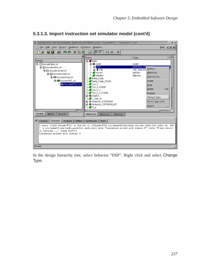
Chapter 5. Embedded Software Design
5.3.1.3. Import instruction set simulator model (cont’d)
In the design hierarchy tree, select behavior "DSP". Right click and selectChangeType.
237
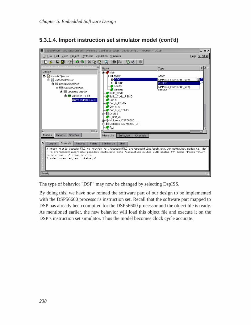
Chapter 5. Embedded Software Design
5.3.1.4. Import instruction set simulator model (cont’d)
The type of behavior "DSP" may now be changed by selecting DspISS.
By doing this, we have now refined the software part of our design to be implementedwith the DSP56600 processor’s instruction set. Recall thatthe software part mapped toDSP has already been compiled for the DSP56600 processor andthe object file is ready.As mentioned earlier, the new behavior will load this objectfile and execute it on theDSP’s instruction set simulator. Thus the model becomes clock cycle accurate.
238
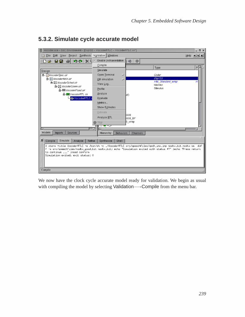
Chapter 5. Embedded Software Design
5.3.2. Simulate cycle accurate model
We now have the clock cycle accurate model ready for validation. We begin as usualwith compiling the model by selectingValidation−→Compile from the menu bar.
239

Chapter 5. Embedded Software Design
5.3.2.1. Simulate cycle accurate model (cont’d)
The model compiles correctly as shown in the logging window.We now proceed tosimulate the model by selectingValidation−→Simulate from the menu bar.
240

Chapter 5. Embedded Software Design
5.3.2.2. Simulate cycle accurate model (cont’d)
Like in the earlier cases, a simulation window pops up. The DSP Instruction set simu-lator can be seen to slow down the simulation speed considerably. This is because thesimulation is being done one instruction at a time in contrast to the high level simulationwe had earlier.
241
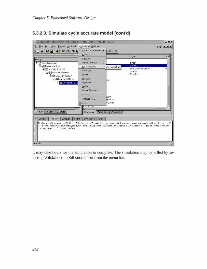
Chapter 5. Embedded Software Design
5.3.2.3. Simulate cycle accurate model (cont’d)
It may take hours for the simulation to complete. The simulation may be killed by se-lectingValidation−→Kill simulation from the menu bar.
242

Chapter 5. Embedded Software Design
5.3.2.4. Simulate cycle accurate model (cont’d)
The demo has now concluded. To exit the SoC environment, select Project−→Exit fromthe menu bar.
243

Chapter 5. Embedded Software Design
5.4. SummaryIn this tutorial, we performed the SW synthesis task after RTL synthesis of HW. Notethat these two tasks are orthogonal and may be done in any order. We showed C codegeneration for the behaviors mapped to SW component. This isa useful feature of SCE,since we can generate C code which can be compiled onto any processor to generateassembly. The code can then used for an instruction set simulator to run on a cycle-by-cycle basis with the RTL HW. All these built in features ofSCE allow the designerto move across abstraction levels even for parts of a design.The flexibility and designcapablity that is thus provided to the designer is enormous.
244
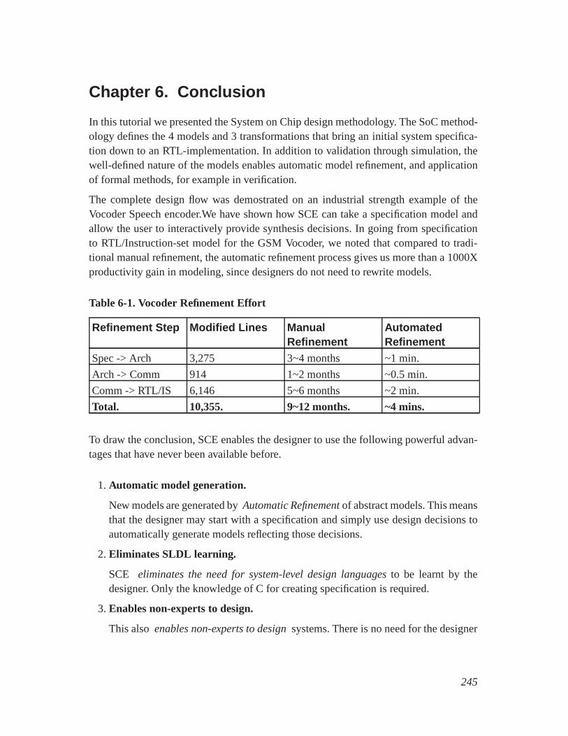
Chapter 6. Conclusion
In this tutorial we presented the System on Chip design methodology. The SoC method-ology defines the 4 models and 3 transformations that bring aninitial system specifica-tion down to an RTL-implementation. In addition to validation through simulation, thewell-defined nature of the models enables automatic model refinement, and applicationof formal methods, for example in verification.
The complete design flow was demostrated on an industrial strength example of theVocoder Speech encoder.We have shown how SCE can take a specification model andallow the user to interactively provide synthesis decisions. In going from specificationto RTL/Instruction-set model for the GSM Vocoder, we noted that compared to tradi-tional manual refinement, the automatic refinement process gives us more than a 1000Xproductivity gain in modeling, since designers do not need to rewrite models.
Table 6-1. Vocoder Refinement Effort
Refinement Step Modified Lines ManualRefinement
AutomatedRefinement
Spec -> Arch 3,275 3~4 months ~1 min.
Arch -> Comm 914 1~2 months ~0.5 min.
Comm -> RTL/IS 6,146 5~6 months ~2 min.
Total. 10,355. 9~12 months. ~4 mins.
To draw the conclusion, SCE enables the designer to use the following powerful advan-tages that have never been available before.
1. Automatic model generation.
New models are generated byAutomatic Refinementof abstract models. This meansthat the designer may start with a specification and simply use design decisions toautomatically generate models reflecting those decisions.
2. Eliminates SLDL learning.
SCE eliminates the need for system-level design languagesto be learnt by thedesigner. Only the knowledge of C for creating specificationis required.
3. Enables non-experts to design.
This also enables non-experts to designsystems. There is no need for the designer
245
Chapter 6. Conclusion
to worry about design details like protocol timing diagrams, low level interfaces etc.Consequently,software developers can design hardwareand hardware designerscan develop software.
4. Supports platforms.
SCE is great forplatform based design. By limiting the choice of components andbusses, designers may select their favorite architecture and then play around withdifferent partitioning schema.
5. Customized methodology.
SCE can also becustomized to any methodologyas per the designer’s choice ofcomponents, system architecture, models and levels of abstraction.
6. Enables IP trading.
SCE simplifies IP trading to a great extent by allowing interoperability at systemlevel. With well defined wrappers, the designer can plug and play with suitable IPsin the design process. If an IP meets the design requirements, the designer maychoose to plug that IP component in the design and not worry about synthesizing orvalidating that part of the design.
246

Appendix A. Frequently Asked Questions
1. What is SCE ?
SCE is an acronym for System-on-Chip Environement. It is a design environementbased on a model refinement methodology. The environment consists of severaltools and user interfaces to help the designer take a functional system specificationto its cycle accurate implementation with minimal effort.
2. What are the supported platforms for SCE ?
SCE 2.2.0 beta is currently supported on Linux RedHat 7.3. The public distributionof the operating system is included on the CD-ROM. SCE has also been tested forRedHat 8.0 and SuSE 8.2 distributions of Linux. Other platforms will be supportedin the future as the need arises.
3. What is the level of expertise needed to design with SCE ?
SCE is designed with the goal of allowing even non-experts toperform system de-sign. A very basic knowledge of SW and HW design, equivalent to an undergraduatedegree in computer engineering, is required to work with SCE.
4. What is the difference between behavior and model ?
A model is a description of the design in a machine readable form (like SpecC).There may be several models used in a system design effort. These models capturethe design with varying levels of abstraction. A behavior, in context of SCE, is a unitof computation. A model is made up by a hierarchy of behaviorsthat communicatewith each other using variables or channels.
5. What are the models that I need ?
In SCE, the designer may start with only a specification model. This model cap-tures the functionality of the design without any implementation details. As we gothrough the design process, various models with greater implementation details aregenerated automatically using the built in tools in SCE. Thedesigner only needsto guide the model generation with decisions. The four primary models in the SCEmethodology are Specification model, Architecture model, Communication modeland Cycle-accurate model. The designer may choose to start with any model as perhis or her choice.
6. What do I need to do with all these models ?
247
Appendix A. Frequently Asked Questions
Each of the models need to be compiled to generate an executable. Once they arecompiled, they need to be simulated to make sure that they work correctly. Thedesigner may choose to view the models in graphical form to understand and verifythe implementation details added as a result of refinement. The specification modelalso needs to be profiled to get useful data for making architectural decisions.
7. How do I get a cycle accurate model of my design ?
The designer may start with any of the system level models, namely the specificationmodel, the architecture model or the communication model. With the help of designdecisions, SCE will generate subsequently refined models ofthe design. The finalmodel generated after RTL refinement and SW compilation willbe a cycle accuratemodel of the design.
8. Why is profiling relevant ?
Profiling is performed to gather useful data about the specification. It gives both aquantitative and a qualitative measure of the computation inside each behavior or aset of behaviors. This information is used to choose the right type and number ofcomponents for the system architecture.
9. How do I discover the "computationally intensive" behaviors in my model ?
A straightforward approach is to produce bar charts for eachleaf behavior in themodel. For a reasonably complex design, the designer can usethe hierarchical na-ture of the behaviors to display comparision between composite behaviors. Behav-iors with low computation may be eliminated. For a behavior with high compu-tation, the designer can display its child behaviors and so on. The author of thespecification model can also supply this information upfront, since he or she wouldbe well conversant with the model.
10.Why should I evaluate an architecture before refinement ?
Most designs have constraints on execution time. The architecture exploration phaserequires the designer to come up with the best set of components (and the distri-bution of computation over them) to meet this constraint. One way would be togenerate the architecture model and then simulate it. This is time consuming if thedesigner has to go over several architectural choices. Evaluation of a model is astatic analysis feature that allows the designer to check ifan architectural choicemeets the design constraints.
11. If my architecture model simulation shows an encoding delayof "0.0ms", whatdid I do wrong ?
248
Appendix A. Frequently Asked Questions
This may be because the specification was not profiled before an architecture modelwas generated. Profiling generates information that allowsarchitecture refinementto insert the appropiate delays for the target component.
12.Can I refine any behavior in a model ?
The behavior which is set as the "top level" of the design is considered for archi-tecture and communication refinement by the tools. Typically, the behavior repre-senting the design under test (without the testbench) is setas the "top level" behav-ior. However, for RTL refinement, the designer may choose a particular behaviormapped to HW. This will allow the designer to examine only an interesting part ofthe design without having to simulate the entire model at cycle accurate level.
13.Why do I need to rename all the generated models ?
Renaming is done to avoid overwriting of models during exploration. Automaticallygenerated models are read-only for the same reason. Renaming also gives a suitablename to the model so that it can be easily recognized in the project window.
14. I want multiple busses in my design. How do I map channels to busses ?
The design example in the tutorial has only one bus. The shortcut for mappingall channels to one bus is to map the top level behavior to thatbus. In case ofmultiple busses, selectSynthesis−→Show Channels after allocating the busses.This would expose all the channels between the components. Individual channelscan then be mapped to respective busses.
15.Can I use point to point wire connections instead of busses inmy design ?
Busses in SCE represent generic connection elements. It is possible to have pointto point connections between components. This can be done simply by includingsuch a point to point protocol in the protocol library and selecting it during com-munication synthesis. During channel mapping the designermust take care to mapchannels between only the relevant components to the point to point "connectionelement."
16.Why do I need to do RTL preprocessing ?
Preprocessing is needed to generate a super finite state machine model of the de-sign, which serves as an input to RTL refinement. The preprocessing step splits thebehaviors into super states, with each super state comprising of a basic block.
17.Why does RTL scheduling and binding display work only for leaf behaviors ?
During preprocessing each leaf behavior under the selectedbehavior for HW im-plemetation is converted to a super FSM. Displaying only onesuper FSM at a time
249

Appendix A. Frequently Asked Questions
avoids overcrowding in the display and state name conflicts.
18.How do I know which RTL units to choose ?
The designer chooses the RTL units that can perform the operations required inthe model. RTL analysis gives statistical information on the number and type ofoperations in each super state. Structural constraints canput lower bound on thenumber of units. For example, if a unit with 3 inputs and 1 output is allocated, thenatleast 4 busses must be allocated for feasible binding.
19.How do I view source code generated by SCE ?
The SpecC source code for the behavior definition can be seen by clicking on the be-havior in the hierarchy tree and selectingView−→Source. The code for the behav-ior instance can be seen by right clicking on the instance in hierarchy and clickingSource. However, SCE also produces C, Verilog and Handel-C files. Since thesefiles do not show up in the hierarchy, they have to be opened externally from a shellusing standard editors.
20.What is the current status of SCE ?
SCE is currently a demo version that works for select examples. In the future, it willbe enhanced to a prototype tool.
21.What other features are planned in the immediate future for SCE ?
In the immediate future, we plan to expand the libraries withmore components, IPsand bus protocols. Improvements are planned for communication synthesis frame-work to handle complex communication architectures. Thereis also work plannedfor OS targetting and generation of RTOS models.
250
References
S. Abdi, J. Peng, R. Doemer, D. Shin, A. Gerstlauer, A. Gluhak, L. Cai, Q. Xie, H. Yu,P. Zhang, and D. Gajski,System-on-Chip Environment - Tutorial, CECS TechnicalReport 02-28, September 24, 2002.
A. Gerstlauer, R. Doemer, J. Peng, and D. Gajski,System Design: A Practical Guidewith SpecC, Kluwer Academic Publishers Inc., June, 2001.
D. Gajski, J. Zhu, R. Doemer, A. Gerstlauer, and S. Zhao,SpecC: Specification Lan-guage and Methodology, Kluwer Academic Publishers Inc., March, 2000.
D. Gajski, F. Vahid, S. Narayan, and J. Gong,Specification and Design of EmbeddedSystems, Prentice Hall, June, 1994.
D. Gajski, F. Vahid, S. Narayan, and J. Gong, “SpecSyn: An Environment Supporting theSpecify-Explore-Refine Paradigm for Hardware/Software System Design”, IEEETransactions on VLSI Systems, Vol. 6, No. 1, pp. 84-100, 1998, Awarded the IEEEVLSI Transactions Best Paper Award, June 2000.
D. Gajski, L. Ramachandran, F. Vahid, S. Narayan, and P. Fung, “100 hour design cycle: A test case”, Proc. Europ. Design Automation Conf. EURO-DAC, 1994.
251

References
252