toshiba cmos digital integrated circuit silicon monolithic t6963cfg · pdf file ·...
TRANSCRIPT
T6963CFG
2007-05-15 1
TOSHIBA CMOS DIGITAL INTEGRATED CIRCUIT SILICON MONOLITHIC
T6963CFG DOT MATRIX LCD CONTROLLER LSI The T6963CFG is an LCD controller designed to be used with LCD control driver LSIs and data display memories. The device has an 8−bit parallel data bus and control lines for reading or writing through an MPU interface. It can be directly connected to a TMPZ−80. It has a 128−word character generator ROM which can control an external display RAM of up to 64 Kbytes. Allocation of text, graphics and external character generator RAM can be made easily and the display window can be moved freely within the allocated memory range. The device supports a very broad range of LCD formats by allowing selection of different combinations via a set of programmable inputs. It can be used in text, graphic and combination text−and−graphic modes, and includes various attribute functions. The T6963CFG is lead (Pb)-free (Sn-Ag) product.
Features Display format (pin−selectable)
Columns : 32, 40, 64, 80 Lines : 2, 4, 6, 8, 10, 12, 14, 16, 20, 24, 28, 32 The combination of number of columns and number of lines must not cause the frequency to exceed 5.5 MHz. (See Fig. 2)
Character font (pin−selectable) Horizontal dots : 5, 6, 7, 8 Vertical dots : 8 (fixed) It is necessary to set a character font in Graphic mode just as in Text mode. The oscillation frequency does not change with the font selection.
Display duty : 1 / 16 to 1 / 128 A 128−word character generator ROM (code 0101) T6963CFG−0101 is built in as standard. External display memory : 64 KB Max
The addresses in display memory of the text area, graphic area and external character generator area are determined by software.
Read or Write operations from the CPU do not disturb the display. A crystal oscillator circuit is built in. The oscillation frequency is adjusted according to the display size. If using
an external clock, use the XI pin as the clock input. (XO open.) External capacitors Crystal oscillation : 20 to 30 pF Ceramic oscillation : 30 to 100 pF Built−in feedback resistor : 900 kΩ (typ.)
Toshiba LCD driver LSIs (other than these with a built−in RAM) can be connected to the device. External display RAM must be static RAM. The T6963CFG cannot refresh D−RAM. The attribute functions can only be used in Text mode. They cannot be used in Graphic or Combination
Character mode.
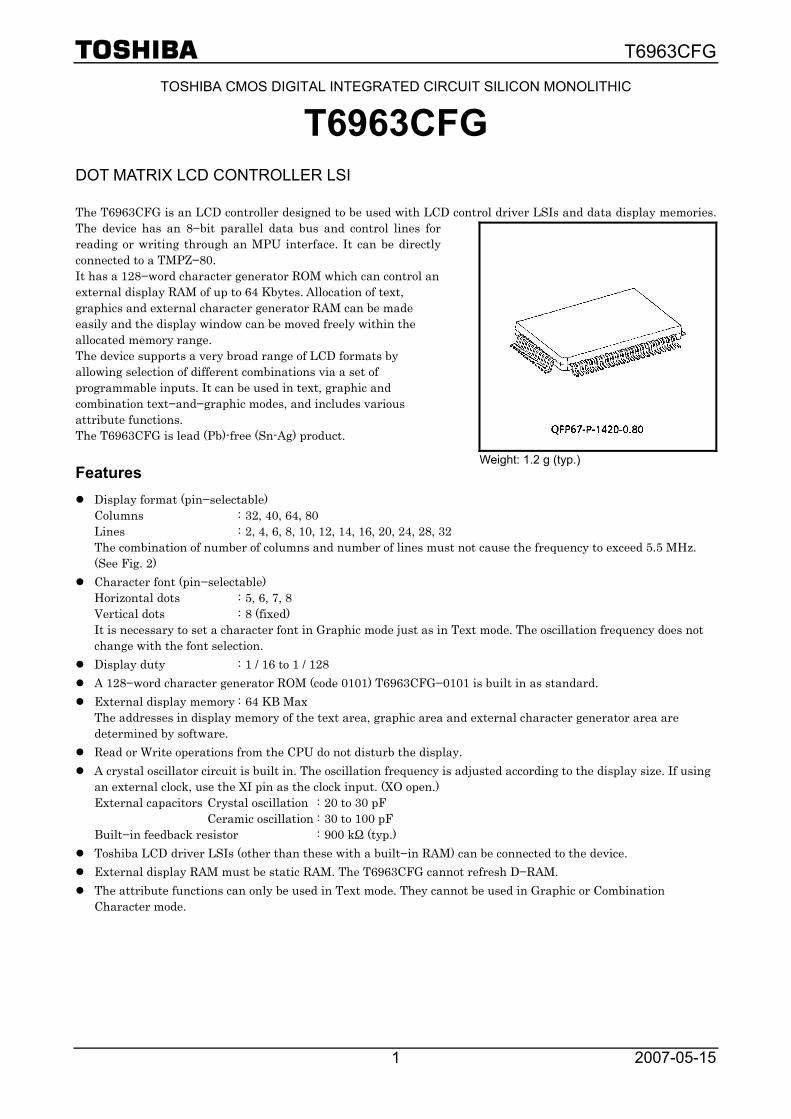
Weight: 1.2 g (typ.)

T6963CFG
2007-05-15 2
Block Diagram

T6963CFG
2007-05-15 3
Pin Assignment
Pin Functions
Pin Name I / O Functions
Pins for selection of LCD size
MDS MD0 MD1
Input
DUAL H H H H H H H H L L L L L L L L
MDS L L L L H H H H L L L L H H H H
MD1 H H L L H H L L H H L L H H L L
MD0 H L H L H L H L H L H L H L H L
LINES 2 4 6 8 10 12 14 16 4 8 12 16 20 24 28 32
V−DOTS 16 32 48 64 80 96 112 128 32 64 96 128 160 192 224 256
1 SCREEN 2 SCREENS
MD2 MD3 Input Pins for selection of number of columns
MD2 H L H L
MD3 H H L L
Columns 32 40 64 80
FS0 FS1 Input Pins for selection of font
FS0 H L H L
FS1 H H L L
Font 5 × 8 6 × 8 7 × 8 8 × 8
D0 to D7 I / O Data I / O pins between CPU and T6963CFG (D7 is MSB)
WR Input Data Write. Write data into T6963CFG when WR = L.
RD Input Data Read. Read data fromT6963CFG when RD = L.
CE Input Chip Enable for T6963CFG. CE must be L when CPU communicates with T6963CFG.

T6963CFG
2007-05-15 4
Pin Name I / O Functions
C / D Input WR = L ······ C / D = H: Command Write C / D = L: Data Write RD = L ······ C / D = H: Status Read C / D = L: Data Read
HALT Input H ······ Normal, L ······ Stops the oscillation of the clock
RESET Input H ······ Normal (T6963CFG has internal pull−up resistor) L ······ Initialize T6963CFG. Text and graphic have addresses and text and graphic area settings are
retained.
DSPON Output Control pin for external DC / DC. DSPON is L when HALT is L or RESET is L. (When DSPON goes H, the column drivers are cleared.)
DUAL Input H ······ Single−Scan L ······ Dual−Scan
DUAL H H L L
SDSEL H L H L
H ······ Sending data by odd / even separation L ······ Sending data by simple serial method
SDSEL Input
Upper screen HOD, ED ED HOD, ED ED
Lower screen ― ― LOD, ED ED
ce0 (LOD)
Output ce0 at DUAL = H Chip enable pin for display memory in the address range 0000H to 07FFH
LOD at DUAL = L Serial data output for odd columns in lower area of LCD
ce1 (LSCP)
Output ce1 at DUAL = H Chip enable pin for display memory in the address range 0800H to 0FFFH
LSCP at DUAL = L Shift clock pulse output for column drivers in lower area of LCD
ce Output Chip enable pin for display memory of any address
d0 to d7 I / O Data I / O pins for display memory
ad0 to ad15 Output Address outputs for display memory (ad15 = L: for upper area of LCD, ad15 = H: for lower area of LCD)
R / W Output Read / Write signal for display memory
ED Output SDSEL = H: Data output for even columns in both upper and lower areas of LCD
SDSEL = L: Data output for columns in both upper and lower areas of LCD
HOD Output Data output for odd columns in upper area of LCD
CDATA Output Synchronous signal for row driver
HSCP Output Shift clock pulse for column driver of upper area of LCD
LP Output Latch pulse for column driver. Shift clock pulse for row driver
FR Output Frame signal
XI Input Crystal oscillator input
XO Output Crystal oscillator output
CH1, CH2 Output Check signal
T1, T2 Input Test input. Usually open
VDD ― Power supply (5.0 V)
VSS ― Power supply (0 V)

T6963CFG
2007-05-15 5
Functional Definition After power on, it is necessary to reset. RESET is kept L between 5 clocks up (oscillation clock). When HALT = L, the oscillation stops. The power supply for the LCD must now be turned off, to protect
the LCD from DC bias. The HALT function includes the RESET function. The column / line counter and display register are cleared by RESET. (Other registers are not cleared.)
Disable the display using the clear−display register. The status must be checked before data or commands are sent. The MSB = 0 status check must be done in
particular. There is a possibility of erroneous operation due to a hard interrupt. STA0 and STA1 must be checked at the same time. When a command is executed, data transmission errors
may occur. The T6963CFG can only handle one byte per machine cycle (16 clocks). It is impossible to send more than
two data in a machine cycle. When using a command with operand data, it important to send the data first, and then execute the
command. The character codes used by the T6963CFG are different from ASCII codes.
T6963CFG
2007-05-15 6
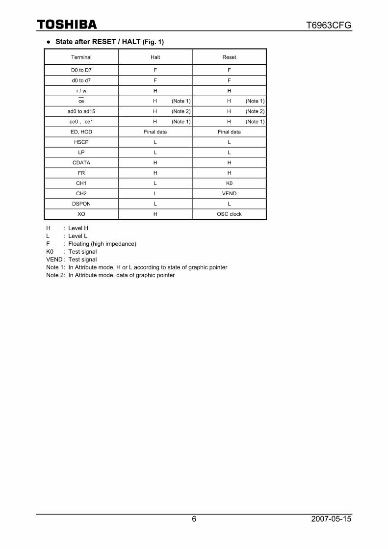
State after RESET / HALT (Fig. 1)
Terminal Halt Reset
D0 to D7 F F
d0 to d7 F F
r / w H H
ce H (Note 1) H (Note 1)
ad0 to ad15 H (Note 2) H (Note 2)
ce0 , ce1 H (Note 1) H (Note 1)
ED, HOD Final data Final data
HSCP L L
LP L L
CDATA H H
FR H H
CH1 L K0
CH2 L VEND
DSPON L L
XO H OSC clock
H : Level H L : Level L F : Floating (high impedance) K0 : Test signal VEND : Test signal Note 1: In Attribute mode, H or L according to state of graphic pointer Note 2: In Attribute mode, data of graphic pointer
T6963CFG
2007-05-15 7
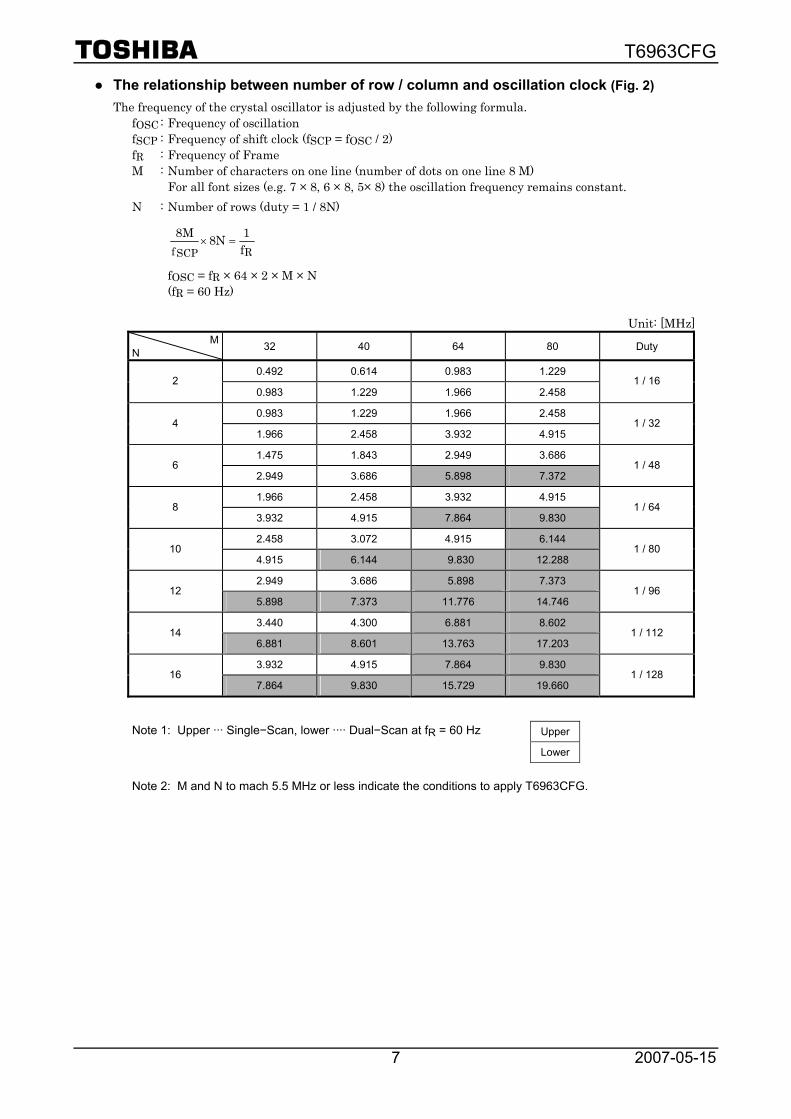
The relationship between number of row / column and oscillation clock (Fig. 2) The frequency of the crystal oscillator is adjusted by the following formula.
fOSC : Frequency of oscillation fSCP : Frequency of shift clock (fSCP = fOSC / 2) fR : Frequency of Frame M : Number of characters on one line (number of dots on one line 8 M)
For all font sizes (e.g. 7 × 8, 6 × 8, 5× 8) the oscillation frequency remains constant. N : Number of rows (duty = 1 / 8N)
RfSCP f1N8M8
=×
fOSC = fR × 64 × 2 × M × N (fR = 60 Hz)
Unit: [MHz]
M N 32 40 64 80 Duty
0.492 0.614 0.983 1.229 2
0.983 1.229 1.966 2.458 1 / 16
0.983 1.229 1.966 2.458 4
1.966 2.458 3.932 4.915 1 / 32
1.475 1.843 2.949 3.686 6
2.949 3.686 5.898 7.372 1 / 48
1.966 2.458 3.932 4.915 8
3.932 4.915 7.864 9.830 1 / 64
2.458 3.072 4.915 6.144 10
4.915 6.144 9.830 12.288 1 / 80
2.949 3.686 5.898 7.373 12
5.898 7.373 11.776 14.746 1 / 96
3.440 4.300 6.881 8.602 14
6.881 8.601 13.763 17.203 1 / 112
3.932 4.915 7.864 9.830 16
7.864 9.830 15.729 19.660 1 / 128
Note 1: Upper ··· Single−Scan, lower ···· Dual−Scan at fR = 60 Hz
Note 2: M and N to mach 5.5 MHz or less indicate the conditions to apply T6963CFG.
Upper
Lower
T6963CFG
2007-05-15 8
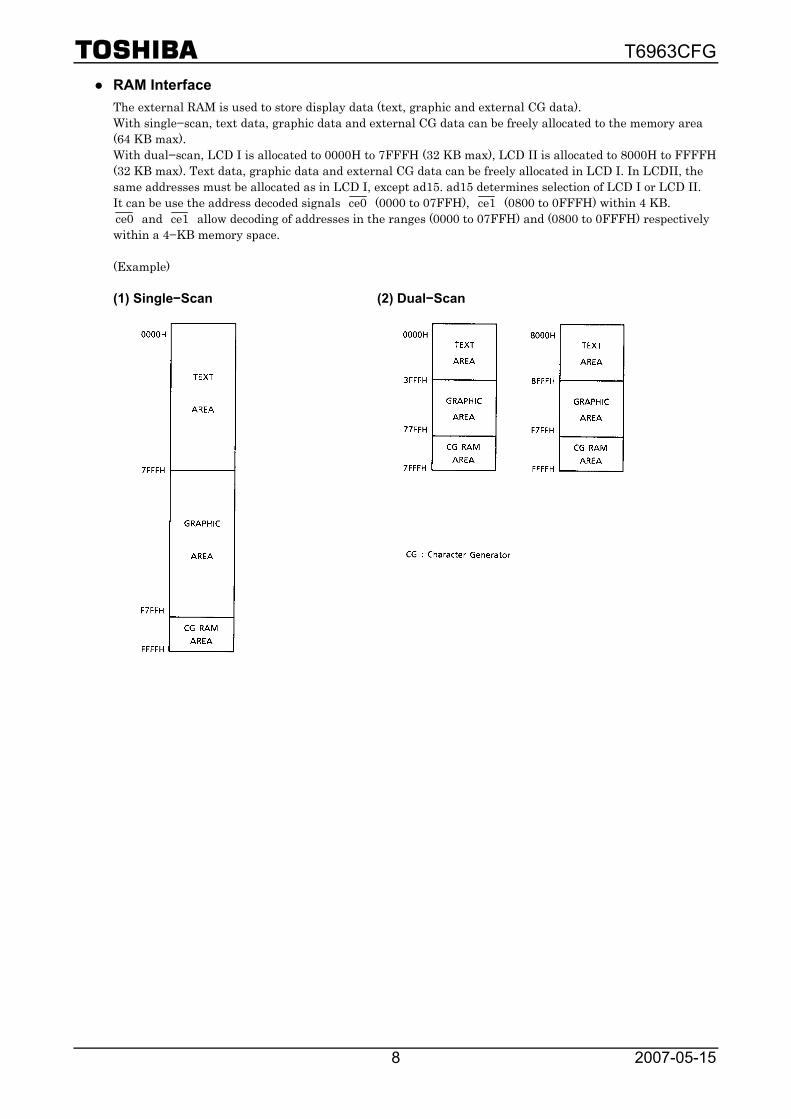
RAM Interface The external RAM is used to store display data (text, graphic and external CG data). With single−scan, text data, graphic data and external CG data can be freely allocated to the memory area (64 KB max). With dual−scan, LCD I is allocated to 0000H to 7FFFH (32 KB max), LCD II is allocated to 8000H to FFFFH (32 KB max). Text data, graphic data and external CG data can be freely allocated in LCD I. In LCDII, the same addresses must be allocated as in LCD I, except ad15. ad15 determines selection of LCD I or LCD II. It can be use the address decoded signals ce0 (0000 to 07FFH), ce1 (0800 to 0FFFH) within 4 KB. ce0 and ce1 allow decoding of addresses in the ranges (0000 to 07FFH) and (0800 to 0FFFH) respectively within a 4−KB memory space.
(Example)
(1) Single−Scan (2) Dual−Scan

T6963CFG
2007-05-15 9
Flowchart of communications with MPU (1) Status Read
A status check must be performed before data is read or written. Status check The Status of T6963CFG can be read from the data lines.
RD L WR H CE L C / D H D0 to D7 Status word
The T6963CFG status word format is as follows:
MSB LSB
STA7 D7
STA6 D6
STA5 D5
STA4 D4
STA3 D3
STA2 D2
STA1 D1
STA0 D0
STA0 Check command execution capability 0: Disable 1: Enable
STA1 Check data read / write capability 0: Disable 1: Enable
STA2 Check Auto mode data read capability 0: Disable 1: Enable
STA3 Check Auto mode data write capability 0: Disable 1: Enable
STA4 Not used
STA5 Check controller operation capability 0: Disable 1: Enable
STA6 Error flag. Used for Screen Peek and Screen copy commands. 0: No error 1: Error
STA7 Check the blink condition 0: Display off 1: Normal display
Note 1: It is necessary to check STA0 and STA1 at the same time. There is a possibility of erroneous operation due to a hardware interrupt.
Note 2: For most modes STA0 / STA1 are used as a status check. Note 3: STA2 and STA3 are valid in Auto mode; STA0 and STA1 are invalid.

T6963CFG
2007-05-15 10
Status checking flow
a) b)
Note 4: When using the MSB = 0 command, a Status Read must be performed. If a status check is not carried out, the T6963CFG cannot operate normally, even after a delay time. The hardware interrupt occurs during the address calculation period (at the end of each line). If a MSB = 0 command is sent to the T6963CFG during this period, the T6963CFG enters Wait status. If a status check is not carried out in this state before the next command is sent, there is the possibility that the command or data will not be received.
(2) Setting data
When using the T6963CFG, first set the data, then set the command.
Procedure for sending a command
a) The case of 1 data b) The case of 2 data
Note: When sending more than two data, the last datum (or last two data) is valid.
T6963CFG
2007-05-15 11
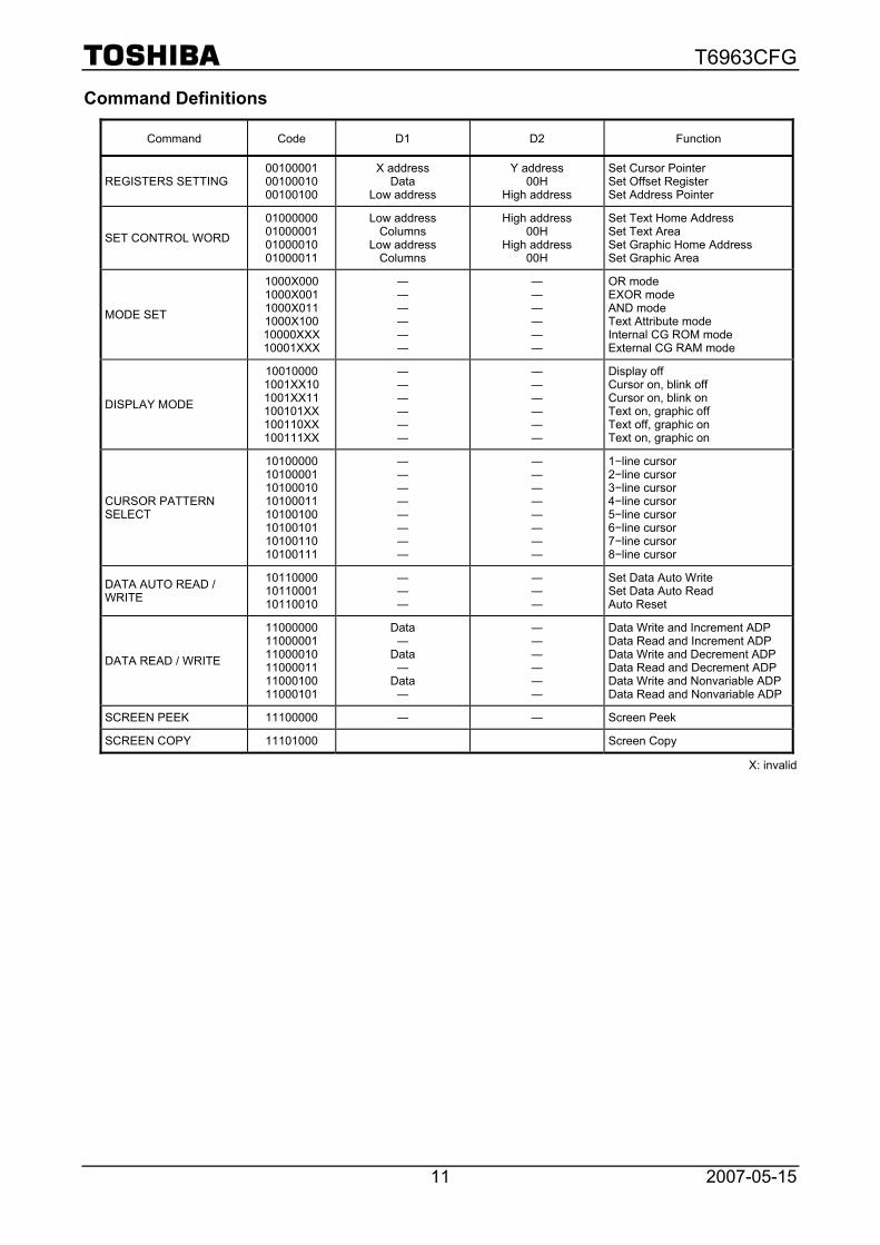
Command Definitions
Command Code D1 D2 Function
REGISTERS SETTING 00100001 00100010 00100100
X address Data
Low address
Y address 00H
High address
Set Cursor Pointer Set Offset Register Set Address Pointer
SET CONTROL WORD
01000000 01000001 01000010 01000011
Low address Columns
Low address Columns
High address 00H
High address 00H
Set Text Home Address Set Text Area Set Graphic Home Address Set Graphic Area
MODE SET
1000X000 1000X001 1000X011 1000X100 10000XXX 10001XXX
― ― ― ― ― ―
― ― ― ― ― ―
OR mode EXOR mode AND mode Text Attribute mode Internal CG ROM mode External CG RAM mode
DISPLAY MODE
10010000 1001XX10 1001XX11 100101XX 100110XX 100111XX
― ― ― ― ― ―
― ― ― ― ― ―
Display off Cursor on, blink off Cursor on, blink on Text on, graphic off Text off, graphic on Text on, graphic on
CURSOR PATTERN SELECT
10100000 10100001 10100010 10100011 10100100 10100101 10100110 10100111
― ― ― ― ― ― ― ―
― ― ― ― ― ― ― ―
1−line cursor 2−line cursor 3−line cursor 4−line cursor 5−line cursor 6−line cursor 7−line cursor 8−line cursor
DATA AUTO READ / WRITE
10110000 10110001 10110010
― ― ―
― ― ―
Set Data Auto Write Set Data Auto Read Auto Reset
DATA READ / WRITE
11000000 11000001 11000010 11000011 11000100 11000101
Data ―
Data ―
Data ―
― ― ― ― ― ―
Data Write and Increment ADP Data Read and Increment ADP Data Write and Decrement ADP Data Read and Decrement ADP Data Write and Nonvariable ADPData Read and Nonvariable ADP
SCREEN PEEK 11100000 ― ― Screen Peek
SCREEN COPY 11101000 Screen Copy
X: invalid
T6963CFG
2007-05-15 12
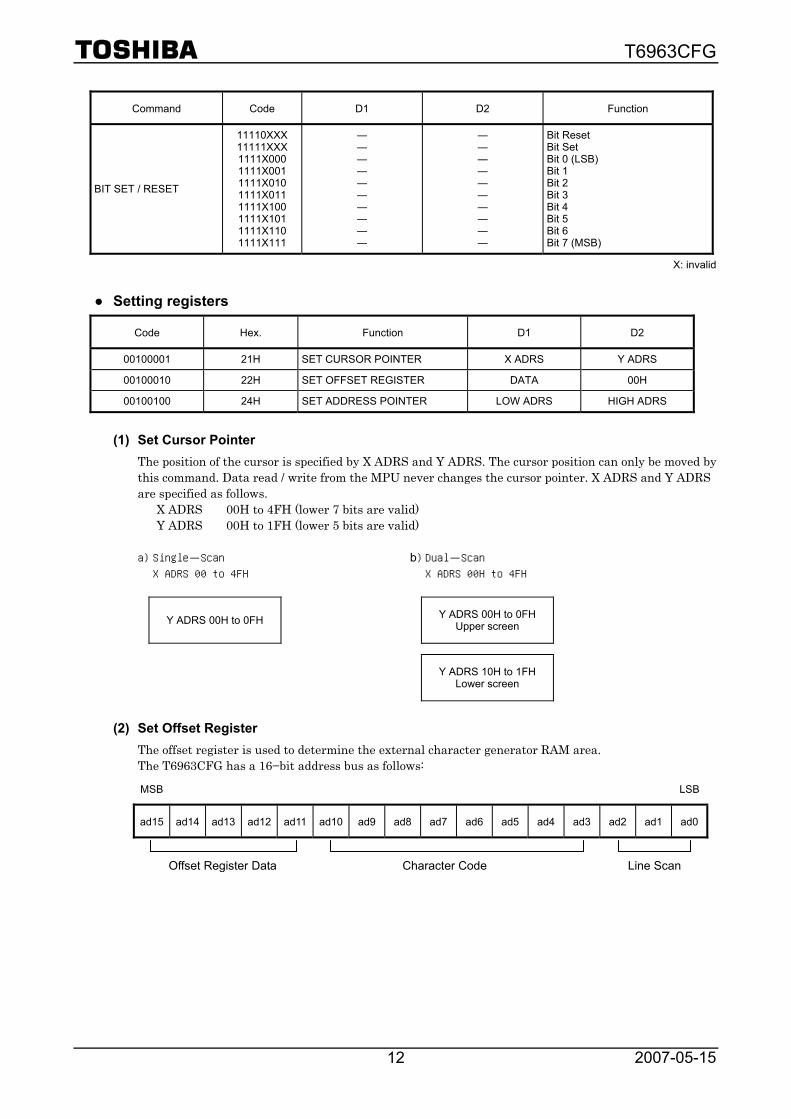
Command Code D1 D2 Function
BIT SET / RESET
11110XXX 11111XXX 1111X000 1111X001 1111X010 1111X011 1111X100 1111X101 1111X110 1111X111
― ― ― ― ― ― ― ― ― ―
― ― ― ― ― ― ― ― ― ―
Bit Reset Bit Set Bit 0 (LSB) Bit 1 Bit 2 Bit 3 Bit 4 Bit 5 Bit 6 Bit 7 (MSB)
X: invalid
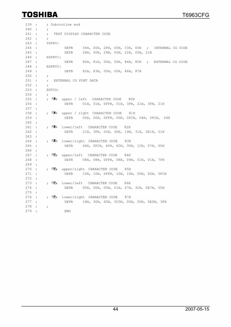
Setting registers
Code Hex. Function D1 D2
00100001 21H SET CURSOR POINTER X ADRS Y ADRS
00100010 22H SET OFFSET REGISTER DATA 00H
00100100 24H SET ADDRESS POINTER LOW ADRS HIGH ADRS
(1) Set Cursor Pointer
The position of the cursor is specified by X ADRS and Y ADRS. The cursor position can only be moved by this command. Data read / write from the MPU never changes the cursor pointer. X ADRS and Y ADRS are specified as follows.
X ADRS 00H to 4FH (lower 7 bits are valid) Y ADRS 00H to 1FH (lower 5 bits are valid)
a) Single- Scan
X ADRS 00 to 4FH
Y ADRS 00H to 0FH
b) Dual- Scan X ADRS 00H to 4FH
Y ADRS 00H to 0FH Upper screen
Y ADRS 10H to 1FH Lower screen
(2) Set Offset Register
The offset register is used to determine the external character generator RAM area. The T6963CFG has a 16−bit address bus as follows:
MSB LSB
ad15 ad14 ad13 ad12 ad11 ad10 ad9 ad8 ad7 ad6 ad5 ad4 ad3 ad2 ad1 ad0
Offset Register Data Character Code Line Scan
T6963CFG
2007-05-15 13
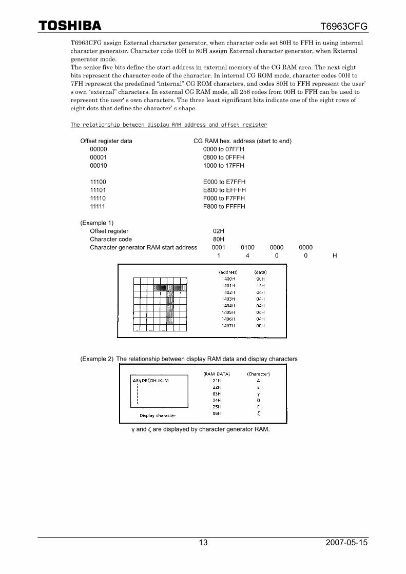
T6963CFG assign External character generator, when character code set 80H to FFH in using internal character generator. Character code 00H to 80H assign External character generator, when External generator mode. The senior five bits define the start address in external memory of the CG RAM area. The next eight bits represent the character code of the character. In internal CG ROM mode, character codes 00H to 7FH represent the predefined “internal” CG ROM characters, and codes 80H to FFH represent the user’ s own “external” characters. In external CG RAM mode, all 256 codes from 00H to FFH can be used to represent the user' s own characters. The three least significant bits indicate one of the eight rows of eight dots that define the character’ s shape.
The relationship between display RAM address and offset register
Offset register data CG RAM hex. address (start to end)
00000 0000 to 07FFH 00001 0800 to 0FFFH 00010 1000 to 17FFH
11100 E000 to E7FFH 11101 E800 to EFFFH 11110 F000 to F7FFH 11111 F800 to FFFFH
(Example 1)
Offset register 02H Character code 80H Character generator RAM start address 0001 0100 0000 0000 1 4 0 0 H
(Example 2) The relationship between display RAM data and display characters
γ and ζ are displayed by character generator RAM.
T6963CFG
2007-05-15 14
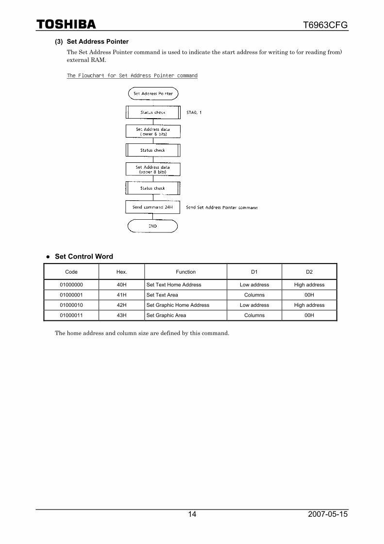
(3) Set Address Pointer The Set Address Pointer command is used to indicate the start address for writing to (or reading from) external RAM.
The Flowchart for Set Address Pointer command
Set Control Word
Code Hex. Function D1 D2
01000000 40H Set Text Home Address Low address High address
01000001 41H Set Text Area Columns 00H
01000010 42H Set Graphic Home Address Low address High address
01000011 43H Set Graphic Area Columns 00H
The home address and column size are defined by this command.
T6963CFG
2007-05-15 15
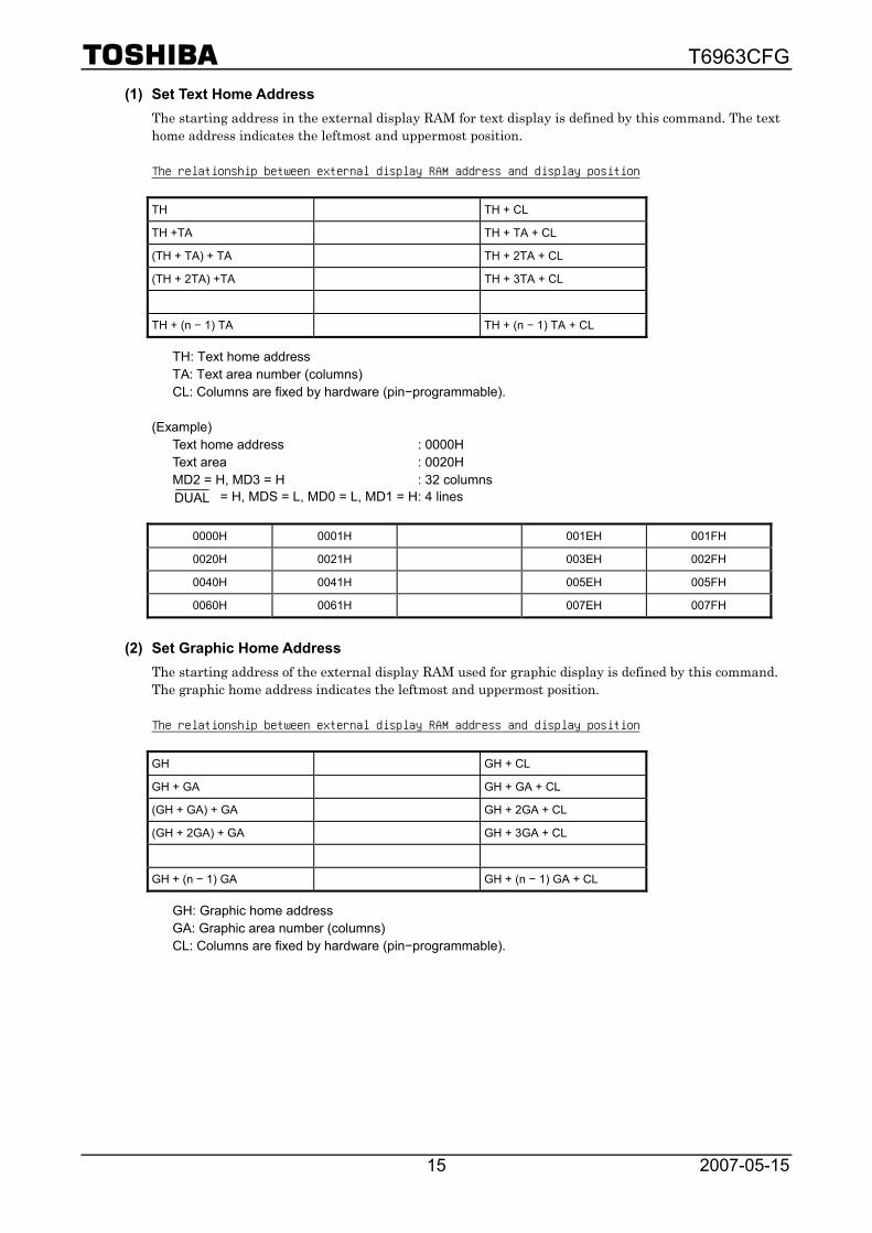
(1) Set Text Home Address The starting address in the external display RAM for text display is defined by this command. The text home address indicates the leftmost and uppermost position.
The relationship between external display RAM address and display position
TH TH + CL
TH +TA TH + TA + CL
(TH + TA) + TA TH + 2TA + CL
(TH + 2TA) +TA TH + 3TA + CL
TH + (n − 1) TA TH + (n − 1) TA + CL
TH: Text home address TA: Text area number (columns) CL: Columns are fixed by hardware (pin−programmable).
(Example)
Text home address : 0000H Text area : 0020H MD2 = H, MD3 = H : 32 columns DUAL = H, MDS = L, MD0 = L, MD1 = H : 4 lines
0000H 0001H 001EH 001FH
0020H 0021H 003EH 002FH
0040H 0041H 005EH 005FH
0060H 0061H 007EH 007FH
(2) Set Graphic Home Address
The starting address of the external display RAM used for graphic display is defined by this command. The graphic home address indicates the leftmost and uppermost position.
The relationship between external display RAM address and display position
GH GH + CL
GH + GA GH + GA + CL
(GH + GA) + GA GH + 2GA + CL
(GH + 2GA) + GA GH + 3GA + CL
GH + (n − 1) GA GH + (n − 1) GA + CL
GH: Graphic home address GA: Graphic area number (columns) CL: Columns are fixed by hardware (pin−programmable).

T6963CFG
2007-05-15 16
(Example) Graphic home address : 0000H Graphic area : 0020H MD2 = H, MD3 = H : 32 columns DUAL = H, MDS = L, MD0 = H, MD1 = H : 2 lines
0000H 0001H 001EH 001FH
0020H 0021H 003EH 003FH
0040H 0041H 005EH 005FH
0060H 0061H 007EH 007FH
0080H 0081H 009EH 009FH
00A0H 00A1H 00BEH 00BFH
00C0H 00C1H 00DEH 00DFH
00E0H 00E1H 00FEH 00FFH
0100H 0101H 011EH 011FH
0120H 0121H 013EH 013FH
0140H 0141H 015EH 015FH
0160H 0161H 017EH 017FH
0180H 0181H 019EH 019FH
01A0H 01A1H 01BEH 01BFH
01C0H 01C1H 01DEH 01DFH
01E0H 01E1H 01FEH 01FFH
(3) Set Text Area
The display columns are defined by the hardware setting. This command can be used to adjust the columns of the display.
(Example)
LCD size : 20 columns, 4 lines Text home address : 0000H Text area : 0014H MD2 = H, MD3 = H : 32 columns DUAL = H, MDS = L, MD0 = L, MD1 = H : 4 lines
0000 0001 ········· 0013 0014 ········· 001F
0014 0015 ········· 0027 0028 ········· 0033
0028 0029 ········· 003B 003C ········· 0047
003C 003D ········· 004F 0050 ········· 005B
LCD
T6963CFG
2007-05-15 17
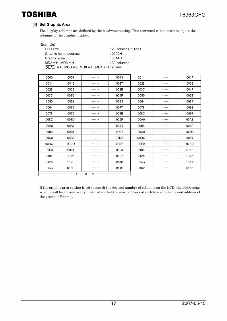
(4) Set Graphic Area The display columns are defined by the hardware setting. This command can be used to adjust the columns of the graphic display.
(Example)
LCD size : 20 columns, 2 lines Graphic home address : 0000H Graphic area : 0014H MD2 = H, MD3 = H : 32 columns DUAL = H, MDS = L, MD0 = H, MD1 = H : 2 lines
0000 0001 ········· 0013 0014 ········· 001F
0014 0015 ········· 0027 0028 ········· 0033
0028 0029 ········· 003B 003C ········· 0047
003C 003D ········· 004F 0050 ········· 005B
0050 0051 ········· 0063 0064 ········· 006F
0064 0065 ········· 0077 0078 ········· 0083
0078 0079 ········· 008B 008C ········· 0097
008C 008D ········· 009F 00A0 ········· 00AB
00A0 00A1 ········· 00B3 00B4 ········· 00BF
00B4 00B5 ········· 00C7 00C8 ········· 00D3
00C8 00C9 ········· 00DB 00DC ········· 00E7
00DC 00DD ········· 00EF 00F0 ········· 00FD
00F0 00F1 ········· 0103 0104 ········· 011F
0104 0105 ········· 0127 0128 ········· 0123
0128 0129 ········· 013B 013C ········· 0147
013C 013D ········· 014F 0150 ········· 015B
If the graphic area setting is set to match the desired number of columns on the LCD, the addressing scheme will be automatically modified so that the start address of each line equals the end address of the previous line + 1.
LCD
T6963CFG
2007-05-15 18
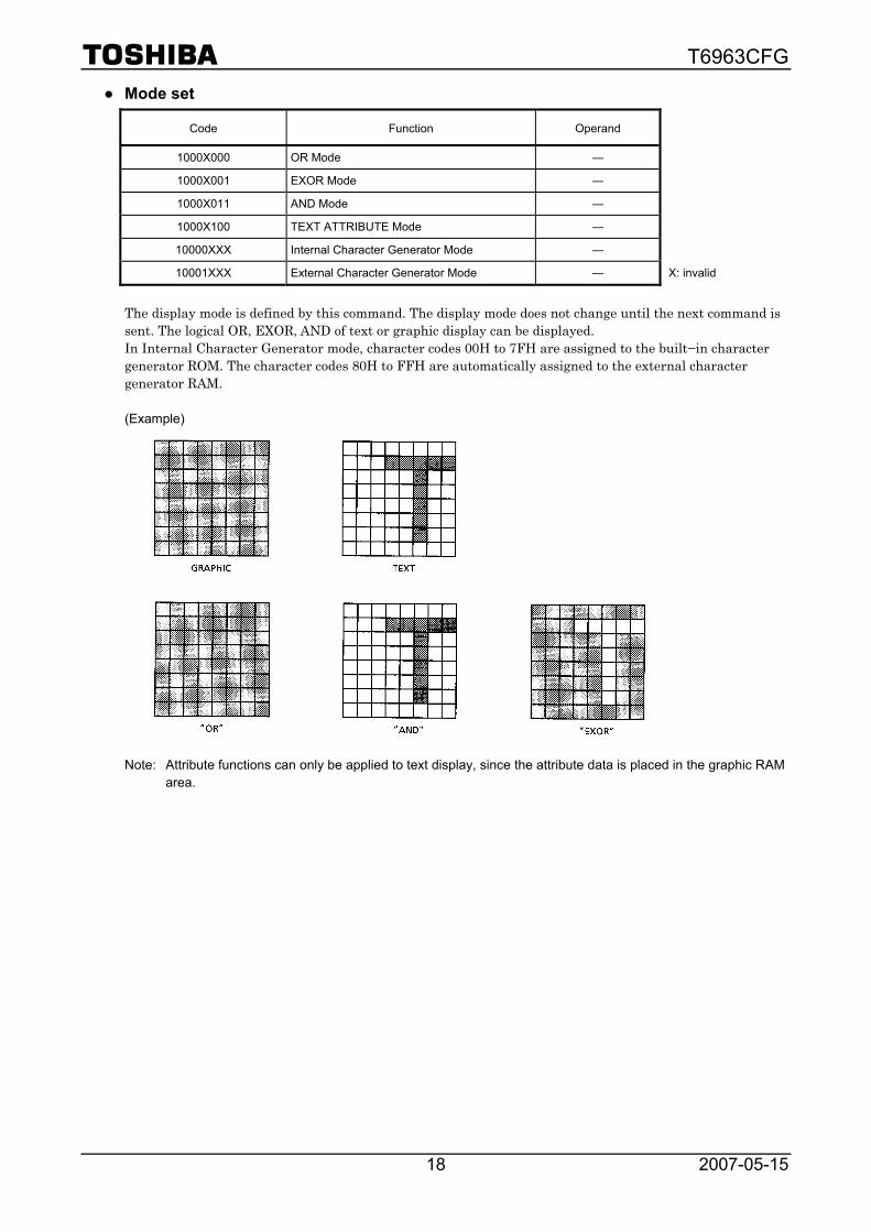
Mode set
Code Function Operand
1000X000 OR Mode ―
1000X001 EXOR Mode ―
1000X011 AND Mode ―
1000X100 TEXT ATTRIBUTE Mode ―
10000XXX Internal Character Generator Mode ―
10001XXX External Character Generator Mode ― X: invalid
The display mode is defined by this command. The display mode does not change until the next command is sent. The logical OR, EXOR, AND of text or graphic display can be displayed. In Internal Character Generator mode, character codes 00H to 7FH are assigned to the built−in character generator ROM. The character codes 80H to FFH are automatically assigned to the external character generator RAM. (Example)
Note: Attribute functions can only be applied to text display, since the attribute data is placed in the graphic RAM area.
T6963CFG
2007-05-15 19
Attribute function
The attribute operations are Reverse display, Character blink and Inhibit. The attribute data is written into the graphic area which was defined by the Set Control Word command. Only text display is possible in Attribute Function mode; graphic display is automatically disabled. However, the Display Mode command must be used to turn both Text and Graphic on in order for the Attribute function to be available. The attribute data for each character in the text area is written to the same address in the graphic area. The Attribute function is defined as follows.
Attribute RAM 1byte X X X X d3 d2 d1 d0
d3 d2 d1 d0 Function
0 0 0 0 Normal display
0 1 0 1 Reverse display
0 0 1 1 Inhibit display
1 0 0 0 Blink of normal display
1 1 0 1 Blink of reverse display X: invalid
1 0 1 1 Blink of inhibit display
Display mode
Code Function Operand
10010000 Display off ―
1001XX10 Cursor on, blink off ―
1001XX11 Cursor on, blink on ―
100101XX Text on, graphic off ―
100110XX Text off, graphic on ― X: invalid
100111XX Text on, graphic on ―
1 0 0 1 D3 D2 D1 D0
Cursor blink on: 1, off: 0 Cursor display on: 1, off: 0 Text display on: 1, off: 0 Graphic display on: 1, off: 0
Note: It is necessary to turn on “Text display” and “Graphic display” in the following cases. a) Combination of text / graphic display b) Attribute function

T6963CFG
2007-05-15 20
Cursor pattern select
Code Function Operand
10100000 1−line cursor ―
10100001 2−line cursor ―
10100010 3−line cursor ―
10100011 4−line cursor ―
10100100 5−line cursor ―
10100101 6−line cursor ―
10100110 7−line cursor ―
10100111 8−line cursor ―
When cursor display is ON, this command selects the cursor pattern in the range 1 line to 8 lines. The cursor address is defined by the Cursor Pointer Set command.
Data Auto Read / Write
Code Hex. Function Operand
10110000 B0H Set Data Auto Write ―
10110001 B1H Set Data Auto Read ―
10110010 B2H Auto Reset ―
This command is convenient for sending a full screen of data from the external display RAM. After setting Auto mode, a Data Write (or Read) command is need not be sent between each datum. A Data Auto Write (or Read) command must be sent after a Set Address Pointer command. After this command, the address pointer is automatically incremented by 1 after each datum. In Auto mode, the T6963CFG cannot accept any other commands. The Auto Reset command must be sent to the T6963CFG after all data has been sent, to clear Auto mode.
T6963CFG
2007-05-15 21
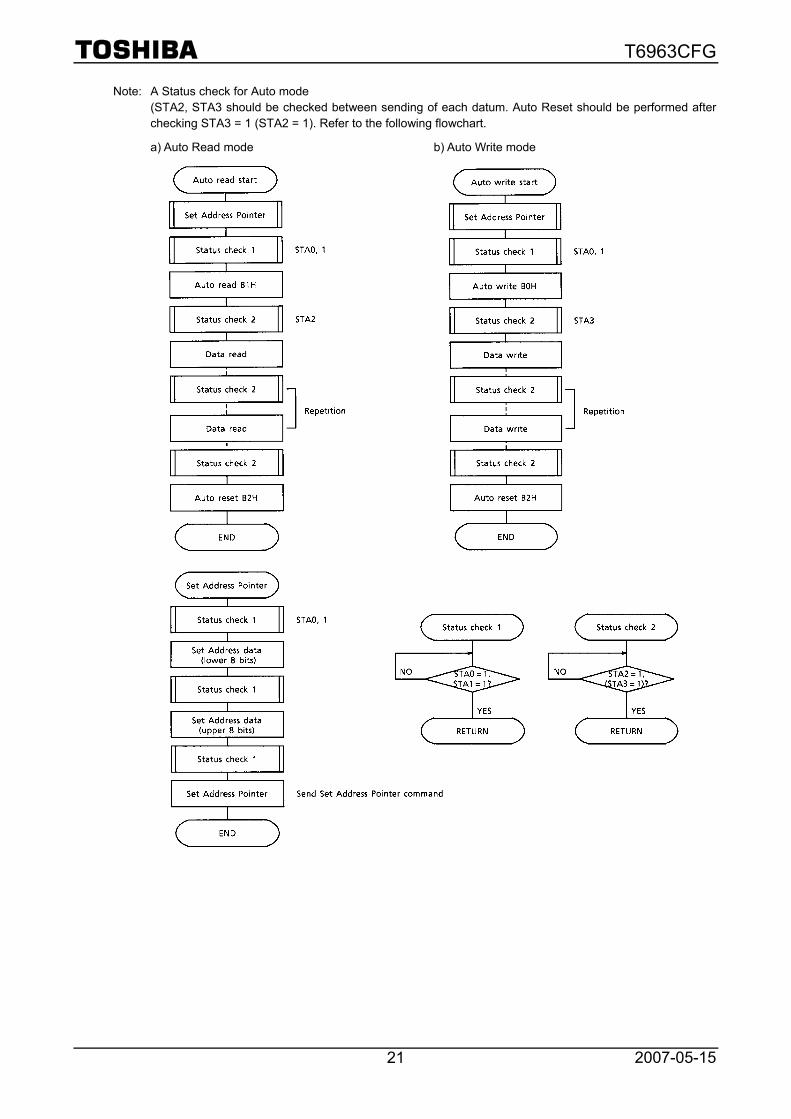
Note: A Status check for Auto mode (STA2, STA3 should be checked between sending of each datum. Auto Reset should be performed after checking STA3 = 1 (STA2 = 1). Refer to the following flowchart.
a) Auto Read mode b) Auto Write mode

T6963CFG
2007-05-15 22
Data Read / Write
Code Hex. Function Operand
11000000 C0H Data Write and Increment ADP Data
11000001 C1H Data Read and Increment ADP ―
11000010 C2H Data Write and Decrement ADP Data
11000011 C3H Data Read and Decrement ADP ―
11000100 C4H Data Write and Nonvariable ADP Data
11000101 C5H Data Read and Nonvariable ADP ―
This command is used for writing data from the MPU to external display RAM, and reading data from external display RAM to the MPU. Data Write / Data Read should be executed after setting address using Set Address Pointer command. The address pointer can be automatically incremented or decremented using this command.
Note: This command is necessary for each 1−byte datum. Refer to the following flowchart.

T6963CFG
2007-05-15 23
Screen Peek
Code Hex. Function Operand
11100000 E0H Screen Peek ―
This command is used to transfer 1 byte of displayed data to the data stack; this byte can then be read from the MPU by data access. The logical combination of text and graphic display data on the LCD screen can be read by this command. The status (STA6) should be checked just after the Screen Peek command. If the address determined by the Set Address Pointer command is not in the graphic area, this command is ignored and a status flag (STA6) is set. Refer to the following flowchart.
Note: This command is available when hardware column number and software column number are the same. Hardware column number is related to MD2 and MD3 setting. Software column number is related to Set Text Area and Set Graphic Area command.
T6963CFG
2007-05-15 24
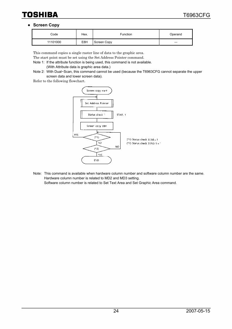
Screen Copy
Code Hex. Function Operand
11101000 E8H Screen Copy ―
This command copies a single raster line of data to the graphic area. The start point must be set using the Set Address Pointer command. Note 1: If the attribute function is being used, this command is not available.
(With Attribute data is graphic area data.) Note 2: With Dual−Scan, this command cannot be used (because the T6963CFG cannot separate the upper
screen data and lower screen data). Refer to the following flowchart.
Note: This command is available when hardware column number and software column number are the same. Hardware column number is related to MD2 and MD3 setting. Software column number is related to Set Text Area and Set Graphic Area command.
T6963CFG
2007-05-15 25
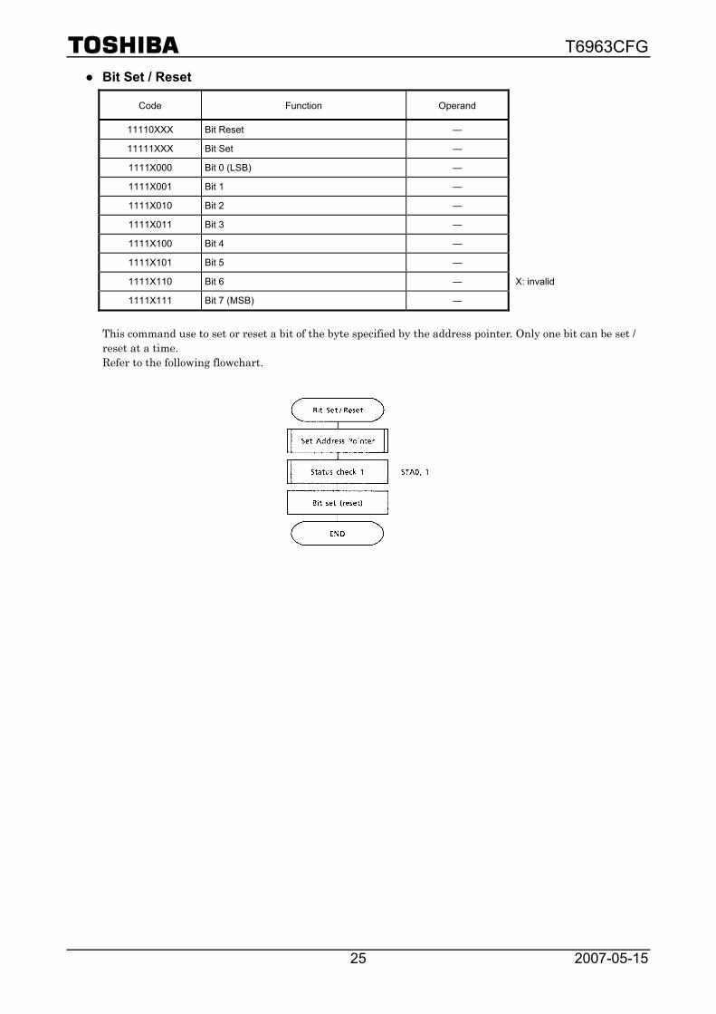
Bit Set / Reset
Code Function Operand
11110XXX Bit Reset ―
11111XXX Bit Set ―
1111X000 Bit 0 (LSB) ―
1111X001 Bit 1 ―
1111X010 Bit 2 ―
1111X011 Bit 3 ―
1111X100 Bit 4 ―
1111X101 Bit 5 ―
1111X110 Bit 6 ― X: invalid
1111X111 Bit 7 (MSB) ―
This command use to set or reset a bit of the byte specified by the address pointer. Only one bit can be set / reset at a time. Refer to the following flowchart.
T6963CFG
2007-05-15 26
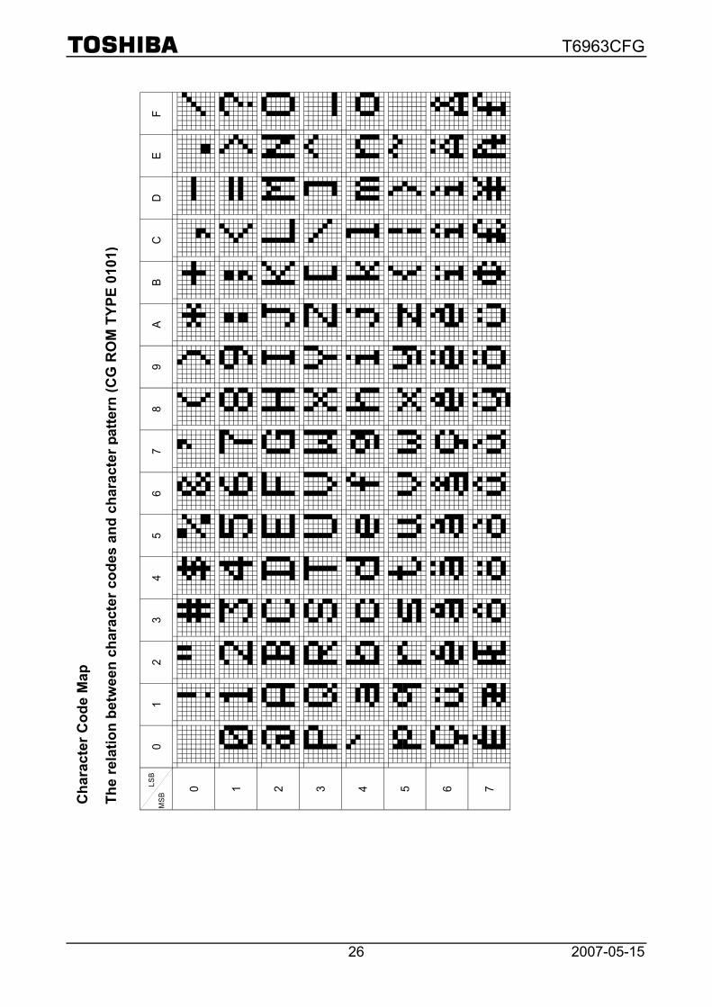
Cha
ract
er C
ode
Map
The
rela
tion
betw
een
char
acte
r cod
es a
nd c
hara
cter
pat
tern
(CG
RO
M T
YPE
0101
)
L
SB
MS
B
73 4 5 6
F
0 1 2
BC
DE
78
A3
45
60
12
9
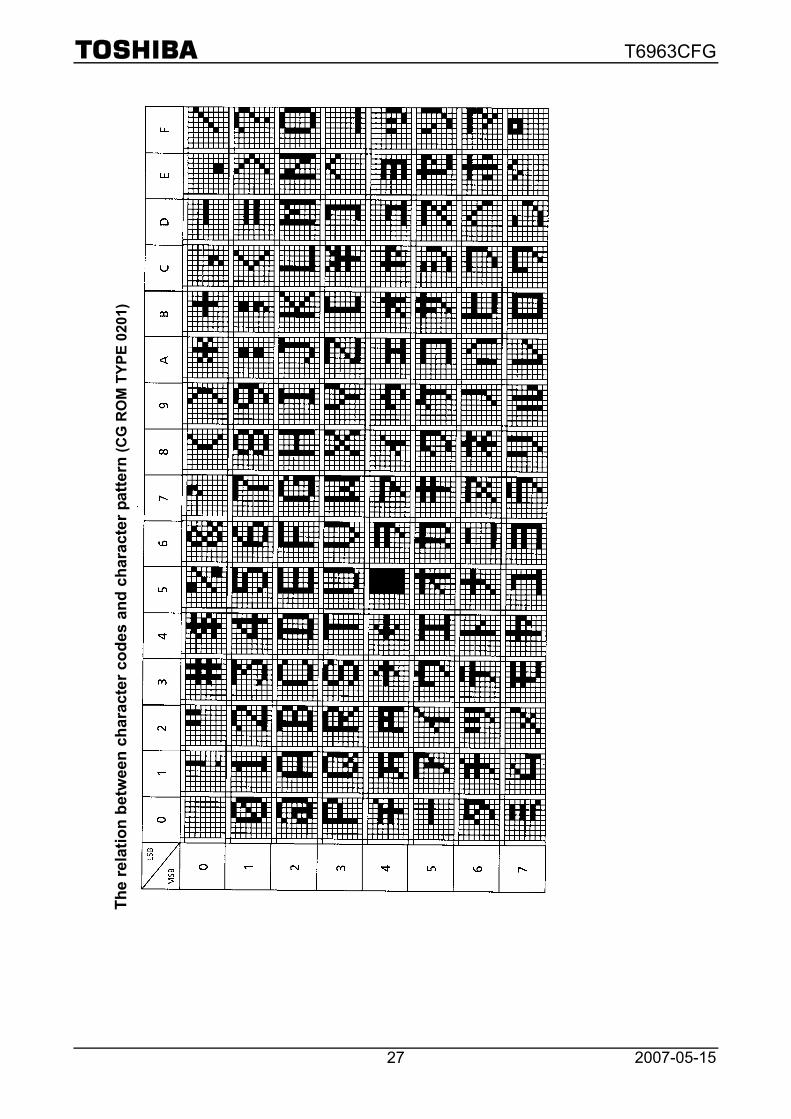
T6963CFG
2007-05-15 27
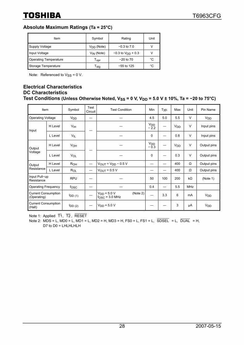
The
rela
tion
betw
een
char
acte
r cod
es a
nd c
hara
cter
pat
tern
(CG
RO
M T
YPE
0201
)
T6963CFG
2007-05-15 28
Absolute Maximum Ratings (Ta = 25°C)
Item Symbol Rating Unit
Supply Voltage VDD (Note) −0.3 to 7.0 V
Input Voltage VIN (Note) −0.3 to VDD + 0.3 V
Operating Temperature Topr −20 to 70 °C
Storage Temperature Tstg −55 to 125 °C
Note: Referenced to VSS = 0 V.
Electrical Characteristics DC Characteristics Test Conditions (Unless Otherwise Noted, VSS = 0 V, VDD = 5.0 V ± 10%, Ta = −20 to 75°C)
Item Symbol Test
Circuit Test Condition Min Typ. Max Unit Pin Name
Operating Voltage VDD ― ― 4.5 5.0 5.5 V VDD
H Level VIH ― VDD − 2.2 ― VDD V Input pins
Input L Level VIL
― ― 0 ― 0.8 V Input pins
H Level VOH ― VDD − 0.3 ― VDD V Output pins
Output Voltage
L Level VOL ―
― 0 ― 0.3 V Output pins
H Level ROH ― VOUT = VDD − 0.5 V ― ― 400 Ω Output pinsOutput Resistance L Level ROL ― VOUT = 0.5 V ― ― 400 Ω Output pins
Input Pull−up Resistance RPU ― ― 50 100 200 kΩ (Note 1)
Operating Frequency fOSC ― ― 0.4 ― 5.5 MHz
Current Consumption (Operating) IDD (1) ― VDD = 5.0 V (Note 2)
fOSC = 3.0 MHz ― 3.3 6 mA VDD
Current Consumption (Halt) IDD (2) ― VDD = 5.0 V ― ― 3 µA VDD
Note 1: Applied T1, T2 , RESET Note 2: MDS = L, MD0 = L, MD1 = L, MD2 = H, MD3 = H, FS0 = L, FS1 = L, SDSEL = L, DUAL = H,
D7 to D0 = LHLHLHLH

T6963CFG
2007-05-15 29
AC Characteristics
Switching Characteristics (1)
Test Conditions (Unless Otherwise Noted, VDD = 5.0 V ± 10%, VSS = 0 V, Ta = −20 to 70°C)
Item Symbol Test Conditions Min Max Unit
Operating Frequency fSCP Ta = −10~70°C ― 2.75 MHz
SCP Pulse Width tCWH, tCWL ― 150 ― ns
SCP Rise / Fall Time tr, tf ― ― 30 ns
LP Set−up Time tLSU ― 150 290 ns
LP Hold Time tLHD ― 5 40 ns
Data Set−up Time tDSU ― 170 ― ns
Data Hold Time tDHD ― 80 ― ns
FR Delay Time td ― 0 90 ns
CDATA Set−up Time tCSU ― 450 850 ns
CDATA Hold Time tCHD ― 450 950 ns
0.9×VDD 0.9×VDD 0.9×VDD
0.9×VDD
0.9×VDD
0.1×VDD
0.1×VDD 0.1×VDD
0.9×VDD
0.1×VDD
0.9×VDD
0.1×VDD
0.9×VDD
0.1×VDD
0.1×VDD0.1×VDD 0.1×VDD
T6963CFG
2007-05-15 30
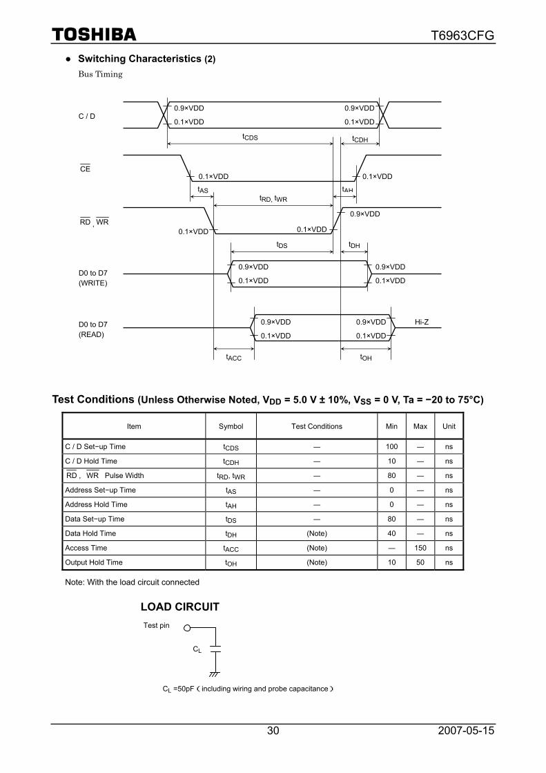
Switching Characteristics (2) Bus Timing
Test Conditions (Unless Otherwise Noted, VDD = 5.0 V ± 10%, VSS = 0 V, Ta = −20 to 75°C)
Item Symbol Test Conditions Min Max Unit
C / D Set−up Time tCDS ― 100 ― ns
C / D Hold Time tCDH ― 10 ― ns
RD , WR Pulse Width tRD, tWR ― 80 ― ns
Address Set−up Time tAS ― 0 ― ns
Address Hold Time tAH ― 0 ― ns
Data Set−up Time tDS ― 80 ― ns
Data Hold Time tDH (Note) 40 ― ns
Access Time tACC (Note) ― 150 ns
Output Hold Time tOH (Note) 10 50 ns
Note: With the load circuit connected
Test pin
CL =50pF(including wiring and probe capacitance)
CL
LOAD CIRCUIT
0.9×VDD
0.1×VDD
tAHtAS tRD, tWR
tDS tDH
tOH tACC
C / D
CE
RD , WR
D0 to D7 (WRITE)
0.9×VDD
0.1×VDD
D0 to D7 (READ)
0.9×VDD
0.1×VDD
0.9×VDD
0.1×VDD
0.9×VDD
0.1×VDD
0.9×VDD
0.1×VDD
0.1×VDD 0.1×VDD
0.1×VDD
tCDS tCDH
Hi-Z
0.9×VDD
0.1×VDD

T6963CFG
2007-05-15 31
Switching Characteristics (3) (1) External RAM Read mode
(2) External RAM Write mode
0.9×VDD
0.1×VDD
0.9×VDD
0.1×VDD 0.1×VDD
0.1×VDD
0.9×VDD 0.9×VDD
0.1×VDD
0.9×VDD
0.1×VDD
0.9×VDD
0.1×VDD 0.1×VDD
0.9×VDD Hi-Z
0.9×VDD
0.1×VDD
0.9×VDD 0.9×VDD
0.1×VDD
0.1×VDD
0.9×VDD 0.9×VDD
0.1×VDD
0.9×VDD
0.1×VDD
0.1×VDD
0.9×VDD
0.1×VDD
0.1×VDD
0.9×VDD
T6963CFG
2007-05-15 32
Test Conditions (Unless Otherwise Noted, VDD = 5.0 V ± 10%, VSS = 0 V, Ta = −20 to 70°C)
Item Symbol Test Conditions Min Max Unit
Address Delay Time td1 ― ― 250 ns
ce Fall Delay Time (Read) td2 ― ― 180 ns
ce Rise Delay Time (Read) td3 ― ― 180 ns
Data Set−up Time tDS ― 0 ― ns
Data Hold Time tDH ― 30 ― ns
ce Fall Delay Time (Write) td4 ― ― 200 ns
ce Rise Delay Time (Write) td5 ― ― 200 ns
r / w Fall Delay Time td6 ― ― 180 ns
r / w Rise Delay Time td7 ― ― 180 ns
Data Stable Time td8 (Note) ― 450 ns
Data Hold Time td9 ― ― 200 ns
Note: With the load circuit connected
Test pin
CL =50pF(including wiring and probe capacitance)
CL
LOAD CIRCUIT

T6963CFG
2007-05-15 33
T6963CFG Example of Application Circuit The T6963CFG can be directly connected to a TMPZ84C00A (Z80 Note 1: CMOS). The T6963CFG can be used with a TMPZ84C00A as shown in the following application circuit.
MPU memory address mapping
Data is transferred to the T6963CFG using a memory request signal.
Address
DATA (I / O) XXXXH
Command / Status XXXX + 1H
Note 1: Z80 is a trademark of Zilog Inc.
T6963CFG
2007-05-15 34
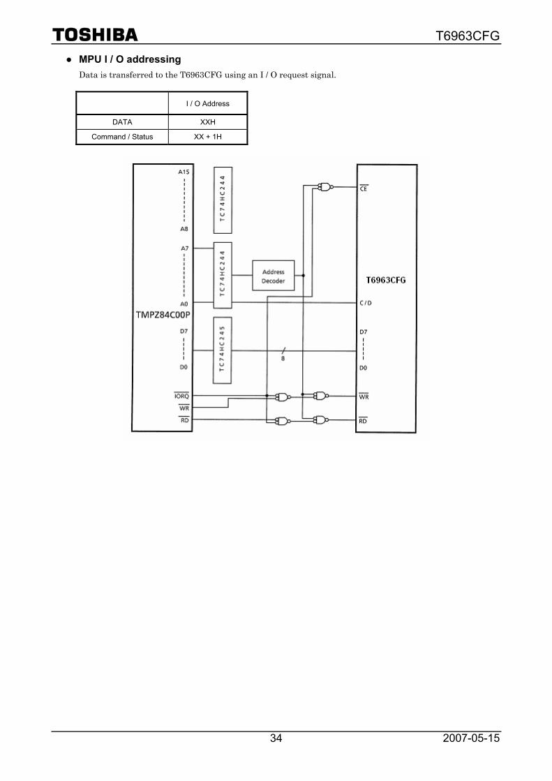
MPU I / O addressing Data is transferred to the T6963CFG using an I / O request signal.
I / O Address
DATA XXH
Command / Status XX + 1H

T6963CFG
2007-05-15 35
When using PPI LSI (TMP82C55) The T6963CFG can be connected to a PPI LSI. The port A connects to the data bus. The port C connects to the control bus. (C / D, CE , WR , RD )

T6963CFG
2007-05-15 36
Application Circuit (1)
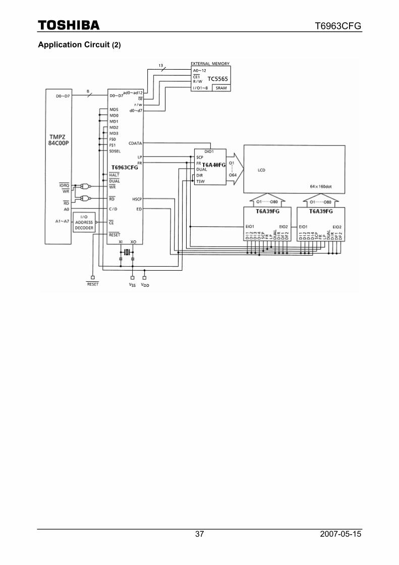
T6963CFG
2007-05-15 37
Application Circuit (2)
T6963CFG
2007-05-15 38
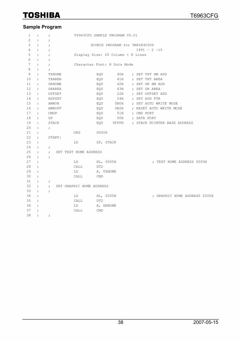
Sample Program 1 : ; T6963CFG SAMPLE PROGRAM V0.01 2 : ; 3 : ; SOURCE PROGRAM for TMPZ84C00P 4 : ; 1991 − 2 −15 5 : ; Display Size: 20 Column × 8 Lines 6 : ; 7 : ; Character Font: 8 Dots Mode 8 : ; 9 : TXHOME EQU 40H ; SET TXT HM ADD 10 : TXAREA EQU 41H ; SET TXT AREA 11 : GRHOME EQU 42H ; SET GR HM ADD 12 : GRAREA EQU 43H ; SET GR AREA 13 : OFFSET EQU 22H ; SET OFFSET ADD 14 : ADPSET EQU 24H ; SET ADD PTR 15 : AWRON EQU 0B0H ; SET AUTO WRITE MODE 16 : AWROFF EQU 0B2H ; RESET AUTO WRITE MODE 17 : CMDP EQU 01H ; CMD PORT 18 : DP EQU 00H ; DATA PORT 19 : STACK EQU 9FFFH ; STACK POINTER BASE ADDRESS 20 : ; 21 : ORG 0000H 22 : START: 23 : LD SP, STACK 24 : ; 25 : ; SET TEXT HOME ADDRESS 26 : ; 27 : LD HL, 0000H ; TEXT HOME ADDRESS 0000H 28 : CALL DT2 29 : LD A, TXHOME 30 : CALL CMD 31 : ; 32 : ; SET GRAPHIC HOME ADDRESS 33 : ; 34 : LD HL, 0200H ; GRAPHIC HOME ADDRESS 0200H 35 : CALL DT2 36 : LD A, GRHOME 37 : CALL CMD 38 : ;

T6963CFG
2007-05-15 39
39 : ; SET TEXT AREA 40 : ; 41 : LD HL, 0014H ; TEXT AREA 20 Columns 42 : CALL DT2 43 : LD A, TXAREA 44 : CALL CMD 45 : ; 46 : ; SET GRAPHIC AREA 47 : ; 48 : LD HL, 0014H ; GRAPHIC AREA 20 Columns 49 : CALL DT2 50 : LD A, GRAREA 51 : CALL CMD 52 : ; 53 : ; MODE SET (OR MODE, Internal Character Generator MODE) 54 : ; 55 : LD A,80H 56 : CALL CMD 57 : ; 58 : ; SET OFFSET REGISTER (00010 10000000 000 = 1400H CG RAM START ADDRESS) 59 : ; CHARACTER CODE 80H 60 : LD HL, 0002H 61 : CALL DT2 62 : LD A, OFFSET 63 : CALL CMD 64 : ; 65 : ; DISPLAY MODE 66 : ; (TEXT ON, GRAPHICS OFF, CURSOR OFF) 67 : ; 68 : LD A, 94H 69 : CALL CMD 70 : ; 71 : ; WRITE TEXT BLANK CODE 72 : ; 73 : LD HL, 0000H ; SET Address Pointer 0000H 74 : CALL DT2 ; (TEXT HOME ADDRESS) 75 : LD A, ADPSET 76 : CALL CMD 77 : 78 : LD A, AWRON ; SET DATA AUTO WRITE
T6963CFG
2007-05-15 40
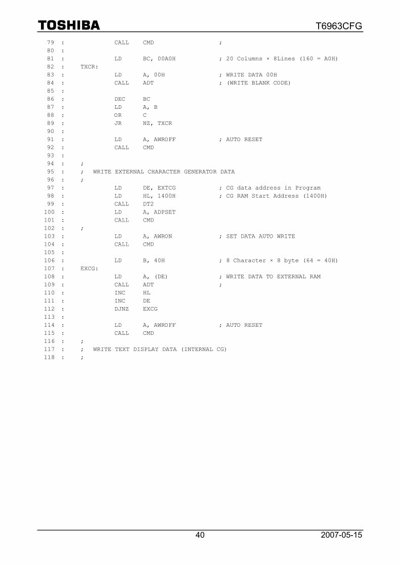
79 : CALL CMD ; 80 : 81 : LD BC, 00A0H ; 20 Columns × 8Lines (160 = A0H) 82 : TXCR: 83 : LD A, 00H ; WRITE DATA 00H 84 : CALL ADT ; (WRITE BLANK CODE) 85 : 86 : DEC BC 87 : LD A, B 88 : OR C 89 : JR NZ, TXCR 90 : 91 : LD A, AWROFF ; AUTO RESET 92 : CALL CMD 93 : 94 : ; 95 : ; WRITE EXTERNAL CHARACTER GENERATOR DATA 96 : ; 97 : LD DE, EXTCG ; CG data address in Program 98 : LD HL, 1400H ; CG RAM Start Address (1400H) 99 : CALL DT2 100 : LD A, ADPSET 101 : CALL CMD 102 : ; 103 : LD A, AWRON ; SET DATA AUTO WRITE 104 : CALL CMD 105 : 106 : LD B, 40H ; 8 Character × 8 byte (64 = 40H) 107 : EXCG: 108 : LD A, (DE) ; WRITE DATA TO EXTERNAL RAM 109 : CALL ADT ; 110 : INC HL 111 : INC DE 112 : DJNZ EXCG 113 : 114 : LD A, AWROFF ; AUTO RESET 115 : CALL CMD 116 : ; 117 : ; WRITE TEXT DISPLAY DATA (INTERNAL CG) 118 : ;
T6963CFG
2007-05-15 41
119 : LD HL, 002BH ; Address Pointer 3 Line, 4 Column 120 : CALL DT2 121 : LD A, ADPSET 122 : CALL CMD 123 : 124 : LD A, AWRON ; SET DATA AUTO WRITE 125 : CALL CMD 126 : 127 : LD B, 0DH ; 13 Character 128 : LD DE, TXPRT 129 : TXLP1: 130 : LD A, (DE) ; WRITE DATA 131 : CALL ADT 132 : INC DE 133 : DJNZ TXLP1 134 : 135 : LD A, AWROFF ; AUTO RESET 136 : CALL CMD 137 : ; 138 : ; WRITE TEXT DISPLAY DATA (EXTERNAL CG upper part) 139 : ; 140 : LD HL, 0057H ; Address Pointer 5 Line, 8 Column 141 : CALL DT2 142 : LD A, ADPSET 143 : CALL CMD 144 : 145 : LD A, AWRON ; SET DATA AUTO WRITE 146 : CALL CMD 147 : 148 : LD B, 06H ; 6 Character 149 : LD DE, EXPRT1 150 : TXLP2: 151 : LD A, (DE) ; WRITE DATA 152 : CALL ADT 153 : INC DE 154 : DJNZ TXLP2 155 : 156 : LD A, AWROFF ; AUTO RESET 157 : CALL CMD 158 : ;
T6963CFG
2007-05-15 42
159 : ; WRITE TEXT DISPLAY DATA (EXTERNAL CG lower part) 160 : ; 161 : LD HL, 006BH ; Address Pointer 6 Line, 8 Column 162 : CALL DT2 163 : LD A, ADPSET 164 : CALL CMD 165 : 166 : LD A, AWRON ; SET DATA AUTO WRITE 167 : CALL CMD 168 : 169 : LD B, 06H ; 6 Character 170 : LD DE, EXPRT2 171 : TXLP3: 172 : LD A, (DE) ; WRITE DATA 173 : CALL ADT 174 : INC DE 175 : DJNZ TXLP3 176 : 177 : LD A, AWROFF ; AUTO RESET 178 : CALL CMD 179 : PEND: 180 : JP PEND ; PROGRAM END 181 : ; 182 : ; Subroutine start 183 : ; 184 : ; COMMAND WRITE ROUTINE 185 : ; 186 : CMD: 187 : PUSH AF 188 : CMD1: IN A, (CMDP) 189 : AND 03H 190 : CP 03H ; STATUS CHECK 191 : JR NZ, CMD1 192 : POP AF 193 : OUT (CMDP), A ; WRITE COMMAND 194 : RET 195 : ; 196 : ; DATA WRITE (1 byte) ROUTINE 197 : ; 198 : DT1:
T6963CFG
2007-05-15 43
199 : PUSH AF 200 : DT11: IN A, (CMDP) 201 : AND 03H 202 : CP 03H ; STATUS CHECK 203 : JR NZ, DT11 204 : POP AF 205 : OUT (DP), A ; WRITE DATA 206 : RET 207 : ; 208 : ; DATA WRITE (2 byte) ROUTINE 209 : ; 210 : DT2: 211 : IN A, (CMDP) 212 : AND 03H 213 : CP 03H ; STATUS CHECK 214 : JR NZ, DT2 215 : LD A, L 216 : OUT (DP), A ; WRITE DATA (D1) 217 : DT21: 218 : IN A, (CMDP) 219 : AND 03H 220 : CP 03H ; STATUS CHECK 221 : JR NZ, DT21 222 : 223 : LD A, H 224 : OUT (DP), A ; WRITE DATA (D2) 225 : RET 226 : ; 227 : ; AUTO WRITE MODE ROUTINE 228 : ; 229 : ADT: 230 : PUSH AF 231 : ADT1: IN A, (CMDP) 232 : AND 08H 233 : CP 08H ; STATUS CHECK 234 : JR NZ, ADT1 235 : POP AF 236 : OUT (DP), A ; WRITE DATA 237 : RET 238 : ;
T6963CFG
2007-05-15 44
239 : ; Subroutine end 240 : ; 241 : ; TEXT DISPLAY CHARACTER CODE 242 : ; 243 : TXPRT: 244 : DEFB 34H, 00H, 2FH, 00H, 33H, 00H ; INTERNAL CG CODE 245 : DEFB 28H, 00H, 29H, 00H, 22H, 00H, 21H 246 : EXPRT1: 247 : DEFB 80H, 81H, 00H, 00H, 84H, 85H ; EXTERNAL CG CODE 248 : EXPRT2: 249 : DEFB 82H, 83H, 00H, 00H, 86H, 87H 250 : ; 251 : ; EXTERNAL CG FONT DATA 252 : ; 253 : EXTCG: 254 : ; 255 : ; upper / left CHARACTER CODE 80H 256 : DEFB 01H, 01H, 0FFH, 01H, 3FH, 21H, 3FH, 21H 257 : 258 : ; upper / right CHARACTER CODE 81H 259 : DEFB 00H, 00H, 0FFH, 00H, 0FCH, 04H, 0FCH, 04H 260 : 261 : ; lower/left CHARACTER CODE 82H 262 : DEFB 21H, 3FH, 05H, 0DH, 19H, 31H, 0E1H, 01H 263 : 264 : ; lower/right CHARACTER CODE 83H 265 : DEFB 04H, 0FCH, 40H, 60H, 30H, 1CH, 07H, 00H 266 : 267 : ; upper/left CHARACTER CODE 84H 268 : DEFB 08H, 08H, 0FFH, 08H, 09H, 01H, 01H, 7FH 269 : 270 : ; upper/right CHARACTER CODE 85H 271 : DEFB 10H, 10H, 0FFH, 10H, 10H, 00H, 00H, 0FCH 272 : 273 : ; lower/left CHARACTER CODE 86H 274 : DEFB 00H, 00H, 00H, 01H, 07H, 3CH, 0E7H, 00H 275 : 276 : ; lower/right CHARACTER CODE 87H 277 : DEFB 18H, 30H, 60H, 0C0H, 00H, 00H, 0E0H, 3FH 278 : ; 279 : END
T6963CFG
2007-05-15 45
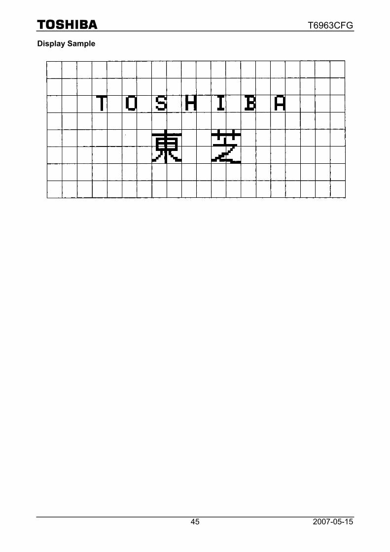
Display Sample

T6963CFG
2007-05-15 46
Package Dimensions
T6963CFG
2007-05-15 47
RESTRICTIONS ON PRODUCT USE
• The information contained herein is subject to change without notice. 021023_D
• TOSHIBA is continually working to improve the quality and reliability of its products. Nevertheless, semiconductor devices in general can malfunction or fail due to their inherent electrical sensitivity and vulnerability to physical stress. It is the responsibility of the buyer, when utilizing TOSHIBA products, to comply with the standards of safety in making a safe design for the entire system, and to avoid situations in which a malfunction or failure of such TOSHIBA products could cause loss of human life, bodily injury or damage to property. In developing your designs, please ensure that TOSHIBA products are used within specified operating ranges as set forth in the most recent TOSHIBA products specifications. Also, please keep in mind the precautions and conditions set forth in the “Handling Guide for Semiconductor Devices,” or “TOSHIBA Semiconductor Reliability Handbook” etc. 021023_A
• The TOSHIBA products listed in this document are intended for usage in general electronics applications (computer, personal equipment, office equipment, measuring equipment, industrial robotics, domestic appliances, etc.). These TOSHIBA products are neither intended nor warranted for usage in equipment that requires extraordinarily high quality and/or reliability or a malfunction or failure of which may cause loss of human life or bodily injury (“Unintended Usage”). Unintended Usage include atomic energy control instruments, airplane or spaceship instruments, transportation instruments, traffic signal instruments, combustion control instruments, medical instruments, all types of safety devices, etc. Unintended Usage of TOSHIBA products listed in this document shall be made at the customer’s own risk. 021023_B
• The products described in this document shall not be used or embedded to any downstream products of which manufacture, use and/or sale are prohibited under any applicable laws and regulations. 060106_Q
• The information contained herein is presented only as a guide for the applications of our products. No responsibility is assumed by TOSHIBA for any infringements of patents or other rights of the third parties which may result from its use. No license is granted by implication or otherwise under any patent or patent rights of TOSHIBA or others. 021023_C
• Please use this product in compliance with all applicable laws and regulations that regulate the inclusion or use of controlled substances. Toshiba assumes no liability for damage or losses occurring as a result of noncompliance with applicable laws and regulations.
• The products described in this document are subject to foreign exchange and foreign trade control laws. 021023_E
• About solderability, following conditions were confirmed Solderability (1) Use of Sn-37Pb solder Bath • solder bath temperature = 230°C • dipping time = 5 seconds • the number of times = once • use of R-type flux (2) Use of Sn-3.0Ag-0.5Cu solder Bath • solder bath temperature = 245°C • dipping time = 5 seconds • the number of times = once • use of R-type flux