ultra ldo 2a linear regulator with adjustable & … ultra ldo 2a linear regulator with...
TRANSCRIPT

AIC1221
Ultra LDO 2A Linear Regulator With
Adjustable & Bypass Pin
Analog Integrations Corporation Si-Soft Research Center DS-1221G-03 20111230
3A1, No.1, Li-Hsin Rd. I, Science Park, Hsinchu 300, Taiwan, R.O.C.
TEL: 886-3-5772500, FAX: 886-3-5772510 www.analog.com.tw 1
FEATURES
Guaranteed 2A Output Current.
Fast Response in Line/Load Transient.
Wide Operating Voltage Ranges: 1.8V to 6V.
0.01µA Shutdown Standby Current.
Low Quiescent Current: 30µA.
Fixed: 1.8V, 2.5V, 3.3V, 5V Output Voltage.
Adjustable Output Voltage are available from 0.8~5.5V.
Low Dropout:550mV at 2A and 3.3V output voltage, 480mV at 2A and 5V output voltage.
High PSRR:70dB at 1kHz.
Active Low or High Shutdown Control. Current Limit and Thermal Protection.
Available in ±2% Output Tolerance.
Available in SOT-223 & TO-252 (3 & 5 pin) and SOP-8 Package.
APPLICATIONS
LCD TV, LCD Monitor, DPF
Networking
STB
DVD, HDD Driver
Portable AV Equipment
PC Peripherals
DESCRIPTION
A low noise, high PSRR and ultra low dropout linear regulator AIC1221 is optimized for low ESR ceramic capacitors operation with 2A continuous
current. The AIC1221 is designed for portable and wireless devices with demanding performance and space requirements.
The AIC1221 offers high precision output voltage of 2% tolerance. Output voltage can also be adjusted for those other than the preset values.
A noise bypass pin is available for further reduction of output noise. The bypass pin could
be floating if it’s unnecessary. At 2A load current and 5V output voltage, a 480mV dropout is performed. The quality of low quiescent current
and low dropout voltage makes this device ideal for battery power applications. The high ripple rejection and low noise of the AIC1221 provide
enhanced performances for critical applications
In addition, a logic-level shutdown input is included, which reduce supply current to 0.01µA
(typ.) in shutdown mode with fast turn-on time less than 100µs. The AIC1221’s current limit and thermal protection provide protection against any
overload condition that would create excessive junction temperatures.
TYPICAL APPLICATION CIRCUIT
VIN1 VOUT 3
GND
AIC1221-33
4.7uFCin
4.7uFCout
Vin Vout3.3V
2
Vin3.3V
VIN2
EN/EN1
VOUT 4
ADJ 5
GND
AIC1221AL-50
4.7uFCin
EN 446kR1
120kR2
Vout
4.7uFCout3
Fixed Linear Regulator Adjustable Linear Regulator

AIC1221
2
TYPICAL APPLICATION CIRCUIT (Continued)
4.7uFCin
4.7uFCout 446k
R1
120kR2
Vin
EN
3.3VVout
100k
RG22nFCbp
EN/EN1
VIN2
VOUT3
ADJ4 GND 5
BP6
PGOOD7
GND8
AIC1221H-33
Adjustable Linear Regulator in SOP-8 Package
ORDERING INFORMATION
PACKING TYPE TR: TAPE & REEL TB: TUBE PACKAGE TYPE
Y3: SOT-223 E3: TO-252
G: Green Package OUTPUT VOLTAGE
18: 1.8V 25: 2.5V
33: 3.3V 50: 5.0V (Of a unit of 0.1V within 0.8~5.5V, additional voltage versions are available on demand)
3 PIN CONFIGURATION
TO-252 (E3) TOP VIEW
1: VIN 2: GND (TAB) 3: VOUT
AIC1221-XXXXX XX
Example: AIC1221-18GY3TR
1.8V Version, in SOT-223 Green
Package & Tape & Reel Packing Type
SOT-223 (Y3) TOP VIEW
1: VIN 2: GND (TAB) 3: VOUT
2 3 1
2 3 1
Example: AIC1221-18GE3TR
1.8V Version, in TO-252 Green Package
& Tape & Reel Packing Type

AIC1221
3
ORDERING INFORMATION (Continued)
PACKING TYPE TR: TAPE & REEL TB: TUBE PACKAGE TYPE
E5: TO-252-5 E5T: TO-252-5
G: Green Package OUTPUT VOLTAGE
18: 1.8V 25: 2.5V 33: 3.3V 50: 5.0V (Of a unit of 0.1V within 0.8~5.5V, additional voltage versions are available on demand) ENABLE TYPE L: Chip Enable Low H: Chip Enable High B: Bypass A: ADJ (For E5 package only)
5 PIN CONFIGURATION AIC1221XX-XXXXXX XX
TO-252-5 (E5) TOP VIEW
1: EN / EN 2: VIN 3: GND (TAB) 4: VOUT 5: BP/ADJ
TO-252-5 (E5T)TOP VIEW
1: EN / EN 2: VIN 3: GND (TAB) 4: VOUT 5: NC
1 2 3 4 5
1 2 3 4 5
Example: AIC1221BH-18GE5TR
With Bypass Pin, Chip Enable High, 1.8V
Version, in TO-252-5 Green Package &
Tape & Reel Packing Type
Example: AIC1221H-18GE5TTR
Chip Enable High, 1.8V Version, in
TO-252-5 Green Package & Tape & Reel
Packing Type

AIC1221
4
ORDERING INFORMATION (Continued)
PACKING TYPE TR: TAPE & REEL TB: TUBE
PACKAGE TYPE R8: SOP-8 Exposed Pad (Heat Sink)
G: Green Package
OUTPUT VOLTAGE 18: 1.8V 25: 2.5V 33: 3.3V 50: 5.0V
(Of a unit of 0.1V within 0.8~5.5V, additional voltage versions are available on demand)
ENABLE TYPE L: Chip Enable Low H: Chip Enable High
8 PIN CONFIGURATION AIC1221X-XXXXXX XX
Example: AIC1221H-18GR8TR
Chip Enable High, 1.8V Version, in SOP-8
Exposed Pad (Heat Sink) Green Package &
Tape & Reel Packing Type
SOP-8 (R8) Exposed Pad (Heat Sink) TOP VIEW
1: EN / EN 2: VIN 3: VOUT 4: ADJ 5: GND (TAB) 6: BP 7: PG 8: GND (TAB)
8
6
5
7
1
3
2
4
GND
AIC1221
5
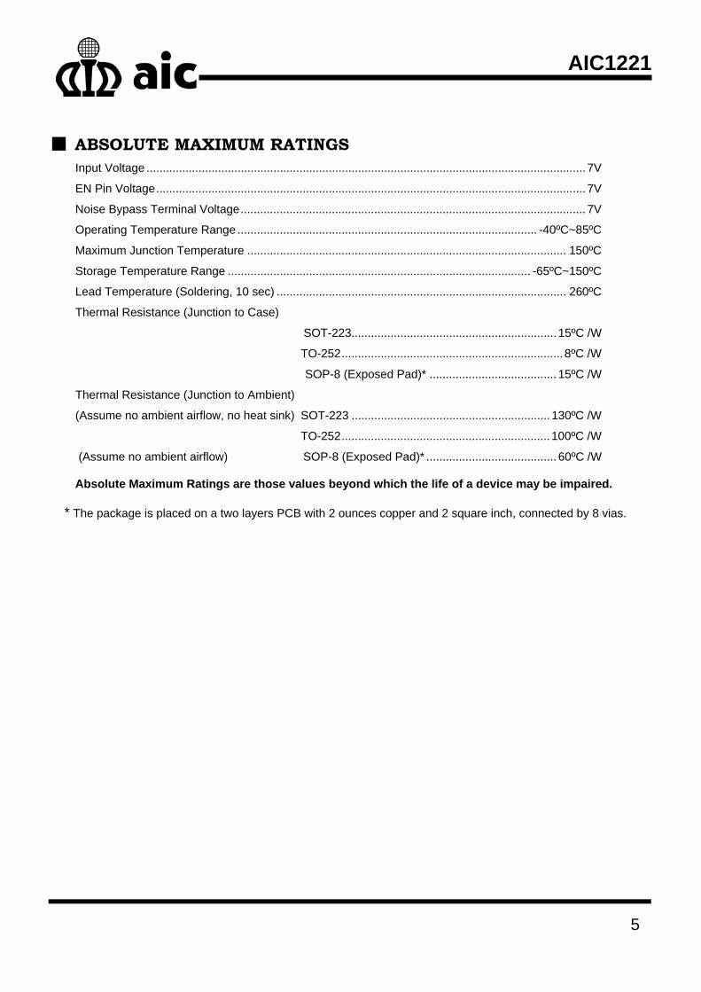
ABSOLUTE MAXIMUM RATINGS Input Voltage ....................................................................................................................................... 7V
EN Pin Voltage.................................................................................................................................... 7V
Noise Bypass Terminal Voltage.......................................................................................................... 7V
Operating Temperature Range ............................................................................................ -40ºC~85ºC
Maximum Junction Temperature .................................................................................................. 150ºC
Storage Temperature Range ............................................................................................. -65ºC~150ºC
Lead Temperature (Soldering, 10 sec) ......................................................................................... 260ºC
Thermal Resistance (Junction to Case)
SOT-223............................................................... 15ºC /W
TO-252....................................................................8ºC /W
SOP-8 (Exposed Pad)* ....................................... 15ºC /W
Thermal Resistance (Junction to Ambient)
(Assume no ambient airflow, no heat sink) SOT-223 ............................................................. 130ºC /W
TO-252................................................................100ºC /W
(Assume no ambient airflow) SOP-8 (Exposed Pad)* ........................................ 60ºC /W
Absolute Maximum Ratings are those values beyond which the life of a device may be impaired.
* The package is placed on a two layers PCB with 2 ounces copper and 2 square inch, connected by 8 vias.
AIC1221
6
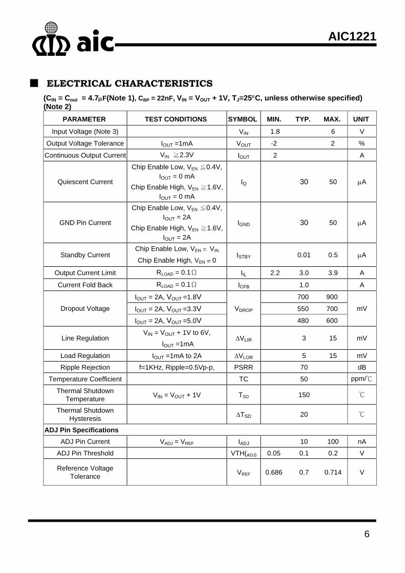
ELECTRICAL CHARACTERISTICS
(CIN = Cout = 4.7F(Note 1), CBP = 22nF, VIN = VOUT + 1V, TJ=25C, unless otherwise specified) (Note 2)
PARAMETER TEST CONDITIONS SYMBOL MIN. TYP. MAX. UNIT
Input Voltage (Note 3) VIN 1.8 6 V
Output Voltage Tolerance IOUT =1mA VOUT -2 2 %
Continuous Output Current VIN ≧2.3V IOUT 2 A
Quiescent Current
Chip Enable Low, VEN ≦0.4V, IOUT = 0 mA
Chip Enable High, VEN ≧1.6V, IOUT = 0 mA
IQ 30 50 A
GND Pin Current
Chip Enable Low, VEN ≦0.4V, IOUT = 2A
Chip Enable High, VEN ≧1.6V, IOUT = 2A
IGND 30 50 A
Standby Current Chip Enable Low, VEN = VIN
Chip Enable High, VEN = 0 ISTBY 0.01 0.5 A
Output Current Limit RLOAD = 0.1Ω IIL 2.2 3.0 3.9 A
Current Fold Back RLOAD = 0.1Ω ICFB 1.0 A
IOUT = 2A, VOUT =1.8V 700 900
IOUT = 2A, VOUT =3.3V 550 700 Dropout Voltage
IOUT = 2A, VOUT =5.0V
VDROP
480 600
mV
Line Regulation VIN = VOUT + 1V to 6V,
IOUT =1mA VLIR 3 15 mV
Load Regulation IOUT =1mA to 2A VLOR 5 15 mV
Ripple Rejection f=1KHz, Ripple=0.5Vp-p, PSRR 70 dB
Temperature Coefficient TC 50 ppm/℃
Thermal Shutdown Temperature
VIN = VOUT + 1V TSD 150 ℃
Thermal Shutdown Hysteresis
TSD 20 ℃
ADJ Pin Specifications
ADJ Pin Current VADJ = VREF IADJ 10 100 nA
ADJ Pin Threshold VTH(ADJ) 0.05 0.1 0.2 V
Reference Voltage Tolerance
VREF 0.686 0.7 0.714 V

AIC1221
7
ELECTRICAL CHARACTERISTICS (Continued)
PARAMETER TEST CONDITIONS SYMBOL MIN. TYP. MAX. UNIT
Shutdown Pin Specifications
Shutdown Pin Current VEN = VIN or GND IEN 0 0.5 A
Shutdown Exit Delay Time IOUT = 30mA t 100 S
Max Output Discharge Resistance to GND during
Shutdown RDSON_
CLMP 20 100 Ω
Chip Enable Low, Output OFF, VIN = 1.6V to 6V
Chip Enable High, Output ON, VIN = 1.6V to 6V
VENH 1.6
Shutdown Input Threshold Chip Enable Low, Output ON,
VIN = 1.6V to 6V
Chip Enable High, Output OFF, VIN = 1.6V to 6V
VENL 0.4
V
Power Good Specifications
PGOOD Rise Threshold 90 93 %
PGOOD Hysteresis 3 10 %
PGOOD Sink Capability IPGOOD=10mA 0.2 0.4 V
PGOOD Delay 0.5 5 ms
Note 1: In the case of Vout <1.8V, 10F Cout is recommended.
Note 2: Specifications are production tested at TA=25°C.pecifications over the -40°C to 85°C operating
temperature range are assured by design, characterization and correlation with Statistical Quality Controls (SQC).
Note 3: Vin(min) is the higher value of Vout + Dropout Voltage or 1.8V.

AIC1221
8
TYPICAL PERFORMANCE CHARACTERISTICS
Fig. 1 Quiescent Current vs. Input Voltage at VOUT=1.8V Fig. 2 Quiescent Current vs. Input Voltage at VOUT=3.3V
Fig. 3 Quiescent Current vs. Temperature at VOUT=1.8V Fig. 4 Quiescent Current vs. Temperature at VOUT=3.3V
Fig. 5 Ground Current vs. Input Voltage at VOUT=1.8V Fig.6 Ground Current vs. Input Voltage at VOUT=3.3V

AIC1221
9
TYPICAL PERFORMANCE CHARACTERISTICS (Continued)
Fig.7 Dropout Voltage at VOUT=1.8V Fig. 8 Dropout Voltage at VOUT=3.3V
Fig. 9 Dropout Voltage at VOUT=5.0V Fig.10 Enable Startup at VOUT=1.8V
Fig.11 Enable Startup at VOUT=3.3V Fig.12 Enable Startup at VOUT=5.0V
Output Voltage
Power Good
Enable Voltage
Output Voltage
Enable Voltage
Output Voltage
Enable Voltage
Power Good
Power Good
AIC1221
10
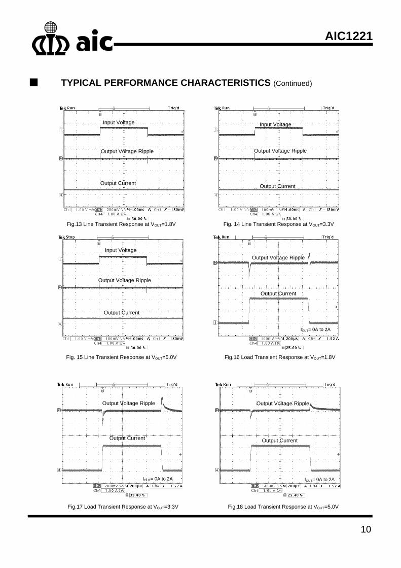
TYPICAL PERFORMANCE CHARACTERISTICS (Continued)
Fig.13 Line Transient Response at VOUT=1.8V Fig. 14 Line Transient Response at VOUT=3.3V
Fig. 15 Line Transient Response at VOUT=5.0V Fig.16 Load Transient Response at VOUT=1.8V
Fig.17 Load Transient Response at VOUT=3.3V Fig.18 Load Transient Response at VOUT=5.0V
Input Voltage
Output Voltage Ripple
Output Current
Output Voltage Ripple
Output Current
Input Voltage
Output Voltage Ripple
Output Current
Output Voltage Ripple
Output Current
IOUT= 0A to 2A IOUT= 0A to 2A
Output Voltage Ripple
Output Current
IOUT= 0A to 2A
Input Voltage
Output Voltage Ripple
Output Current

AIC1221
11
TYPICAL PERFORMANCE CHARACTERISTICS (Continued)
Fig.19 Shutdown Transient at VOUT=1.8V Fig.20 Shutdown Transient at VOUT=3.3V
Fig. 21 Shutdown Transient at VOUT=5.0V Fig.22 Current Fold Back at VOUT=1.8V
Fig. 23 Current Fold Back at VOUT=3.3V Fig.24 PSRR Curve
Enable Voltage
Output Ripple
Power Good
Output Voltage Output Voltage
Enable Voltage Enable Voltage
Power Good Power Good
Output Current
Output Current
Simulation Verified

AIC1221
12
■ BLOCK DIAGRAM
PIN DESCRIPTION VIN – Power supply input pin. Bypass with a 4.7µF capacitor to GND.
GND – Ground.
VOUT – Regulator Output pin. Sources up to 2A.
EN (5 Pin and 8 Pin) – Chip Enable (Active Low). This pin isn’t allowed to float.
EN (5 Pin and 8 Pin) – Chip Enable (Active High). This pin isn’t allowed to float.
BP (5 Pin and 8 Pin) – Bypass pin. It should be connected to external 22nF capacitor to GND to reduce
output noise. The bypass pin could be floating if it’s unnecessary.
PGOOD (8 Pin) – Power Good open Drain output.
ADJ (5 Pin and 8 Pin) – The output voltage can either be set by the internal feedback resistors when this pin
is grounded, or be set by the external feedback resistors when using a resistive
divider.
AIC1221
13
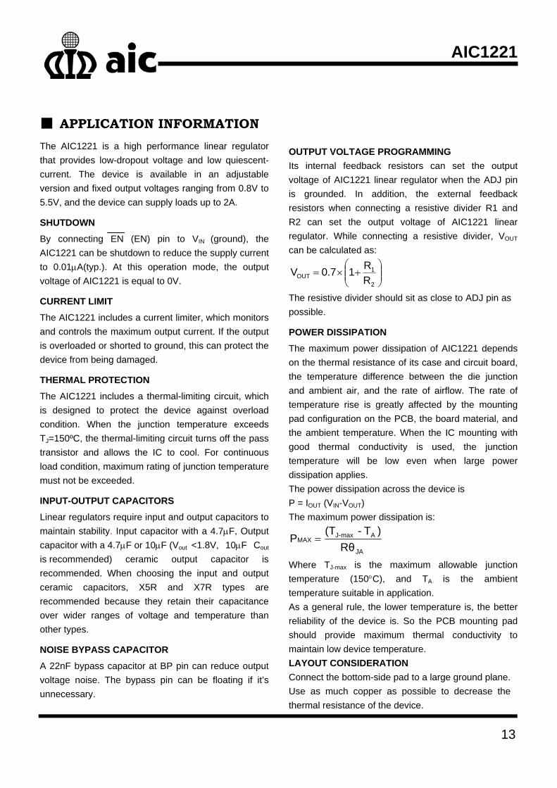
APPLICATION INFORMATION
The AIC1221 is a high performance linear regulator
that provides low-dropout voltage and low quiescent-
current. The device is available in an adjustable
version and fixed output voltages ranging from 0.8V to
5.5V, and the device can supply loads up to 2A.
SHUTDOWN
By connecting EN (EN) pin to VIN (ground), the
AIC1221 can be shutdown to reduce the supply current
to 0.01A(typ.). At this operation mode, the output
voltage of AIC1221 is equal to 0V.
CURRENT LIMIT
The AIC1221 includes a current limiter, which monitors
and controls the maximum output current. If the output
is overloaded or shorted to ground, this can protect the
device from being damaged.
THERMAL PROTECTION
The AIC1221 includes a thermal-limiting circuit, which
is designed to protect the device against overload
condition. When the junction temperature exceeds
TJ=150ºC, the thermal-limiting circuit turns off the pass
transistor and allows the IC to cool. For continuous
load condition, maximum rating of junction temperature
must not be exceeded.
INPUT-OUTPUT CAPACITORS
Linear regulators require input and output capacitors to
maintain stability. Input capacitor with a 4.7F, Output
capacitor with a 4.7F or 10F (Vout <1.8V, 10F Cout
is recommended) ceramic output capacitor is
recommended. When choosing the input and output
ceramic capacitors, X5R and X7R types are
recommended because they retain their capacitance
over wider ranges of voltage and temperature than
other types.
NOISE BYPASS CAPACITOR
A 22nF bypass capacitor at BP pin can reduce output
voltage noise. The bypass pin can be floating if it’s
unnecessary.
OUTPUT VOLTAGE PROGRAMMING
Its internal feedback resistors can set the output
voltage of AIC1221 linear regulator when the ADJ pin
is grounded. In addition, the external feedback
resistors when connecting a resistive divider R1 and
R2 can set the output voltage of AIC1221 linear
regulator. While connecting a resistive divider, VOUT
can be calculated as:
2
1OUT R
R17.0V
The resistive divider should sit as close to ADJ pin as
possible.
POWER DISSIPATION
The maximum power dissipation of AIC1221 depends
on the thermal resistance of its case and circuit board,
the temperature difference between the die junction
and ambient air, and the rate of airflow. The rate of
temperature rise is greatly affected by the mounting
pad configuration on the PCB, the board material, and
the ambient temperature. When the IC mounting with
good thermal conductivity is used, the junction
temperature will be low even when large power
dissipation applies.
The power dissipation across the device is
P = IOUT (VIN-VOUT)
The maximum power dissipation is:
JA
Amax-JMAX
Rθ
)T-(TP
Where TJ-max is the maximum allowable junction
temperature (150C), and TA is the ambient
temperature suitable in application.
As a general rule, the lower temperature is, the better
reliability of the device is. So the PCB mounting pad
should provide maximum thermal conductivity to
maintain low device temperature.
LAYOUT CONSIDERATION
Connect the bottom-side pad to a large ground plane.
Use as much copper as possible to decrease the
thermal resistance of the device.

AIC1221
14
PHYSICAL DIMENSIONS SOT-223 PACKAGE OUTLINE DRAWING
cb
AA2
WITH PLATING
VIEW B
θ
0.25
LSEATING PLANEGAUGE PLANE
A1
BASE METALSECTION A-A
D
E
e1
eA A
b2
E1
SEE VIEW B
Note: 1. Refer to JEDEC TO-261AA. 2. Dimension "D" does not include mold flash, protrusions or gate burrs. Mold flash, protrusion or gate burrs shall not exceed 6 mil per side . 3. Dimension "E1" does not include inter-lead flash or protrusions. 4. Controlling dimension is millimeter, converted inch dimensions are not necessarily exact.
3.30
0°
1.55
0.90
6.70
6.30
0.23
2.90
0.66
0.02
E1
θ
L
e1
e
b2
D
E
c
b
A2
A1
3.70
8°
2.30 BSC
4.60 BSC
1.65
7.30
6.70
0.33
3.10
0.84
0.10
MIN.
SYMBOL
A 1.80
MAX.
SOT-223
MILLIMETERS
AIC1221
15
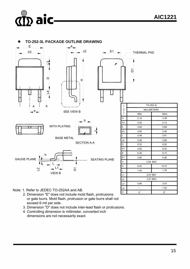
TO-252-3L PACKAGE OUTLINE DRAWING
c2
SEE VIEW B
A
H
b3
AAe
ED
L3L4
c
BASE METAL
WITH PLATING
SEATING PLANE
b
SECTION A-A
VIEW B
A1
LL1
GAUGE PLANE
L2
THERMAL PAD
D1
E1
Note: 1. Refer to JEDEC TO-252AA and AB. 2. Dimension "E" does not include mold flash, protrusions or gate burrs. Mold flash, protrusion or gate burrs shall not exceed 6 mil per side . 3. Dimension "D" does not include inter-lead flash or protrusions. 4. Controlling dimension is millimeter, converted inch dimensions are not necessarily exact.
MILLIMETERS
TO-252-3L
MAX.
2.38A
SYMBOL MIN.
2.19
0.13
5.46
0.61
0.89
6.22
6.73
0.89
2.67 REF
0.51 BSC
10.41
1.78
2.03
1.02
2.28 BSC
A1
b
b3
c2
E
D
c
H
L
L1
L2
L4
L3
e
0.00
4.95
0.46
0.46
5.33
6.35
9.40
1.40
0.89
--
0.64
0° 8°
6.004.60
5.463.90
D1
E1
AIC1221
16
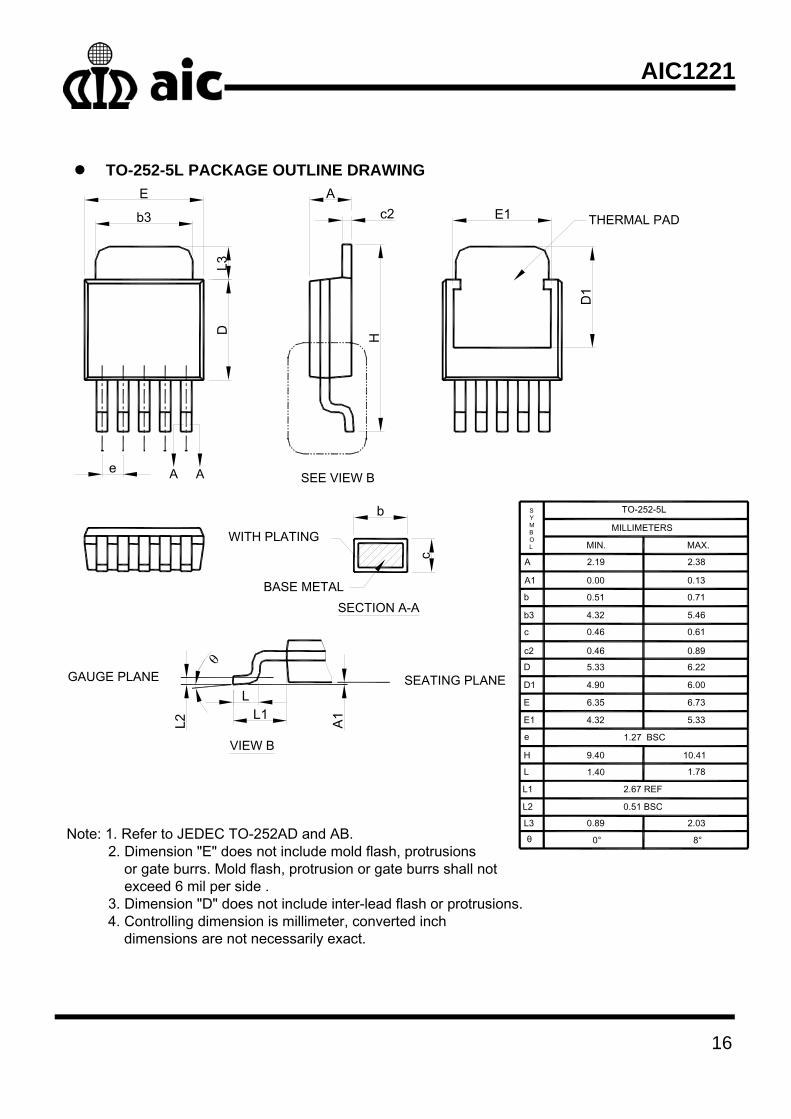
TO-252-5L PACKAGE OUTLINE DRAWING
L2
GAUGE PLANE
L1L
A1
VIEW B
SECTION A-A
b
SEATING PLANE
WITH PLATING
BASE METAL
c
L3D
E
e A A
b3
H
A
SEE VIEW B
c2 THERMAL PAD
D1
E1
Note: 1. Refer to JEDEC TO-252AD and AB. 2. Dimension "E" does not include mold flash, protrusions or gate burrs. Mold flash, protrusion or gate burrs shall not exceed 6 mil per side . 3. Dimension "D" does not include inter-lead flash or protrusions. 4. Controlling dimension is millimeter, converted inch dimensions are not necessarily exact.
0°
0.51
0.89
1.40
9.40
6.35
5.33
0.46
0.46
4.32
0.00
e
L3θ
L2
L1
L
H
c
D
E
c2
b3
b
A1
1.27 BSC
8°
2.03
1.78
10.41
0.51 BSC
2.67 REF
0.71
6.73
6.22
0.89
0.61
5.46
0.13
2.19
MIN.
SYMBOL
A 2.38
MAX.
TO-252-5L
MILLIMETERS
4.90D1 6.00
4.32E1 5.33
AIC1221
17
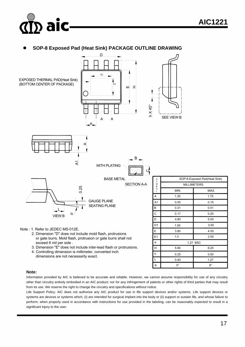
SOP-8 Exposed Pad (Heat Sink) PACKAGE OUTLINE DRAWING
Note: Information provided by AIC is believed to be accurate and reliable. However, we cannot assume responsibility for use of any circuitry
other than circuitry entirely embodied in an AIC product; nor for any infringement of patents or other rights of third parties that may result
from its use. We reserve the right to change the circuitry and specifications without notice.
Life Support Policy: AIC does not authorize any AIC product for use in life support devices and/or systems. Life support devices or
systems are devices or systems which, (I) are intended for surgical implant into the body or (ii) support or sustain life, and whose failure to
perform, when properly used in accordance with instructions for use provided in the labeling, can be reasonably expected to result in a
significant injury to the user.
A
D
LVIEW B
0.25
SEATING PLANE
SECTION A-ABASE METAL
GAUGE PLANE
WITH PLATINGA1
B
C
eA A
HE
D1
E1
EXPOSED THERMAL PAD(Heat Sink)(BOTTOM CENTER OF PACKAGE)
h X
45°
SEE VIEW B
Note : 1. Refer to JEDEC MS-012E. 2. Dimension "D" does not include mold flash, protrusions or gate burrs. Mold flash, protrusion or gate burrs shall not exceed 6 mil per side . 3. Dimension "E" does not include inter-lead flash or protrusions. 4. Controlling dimension is millimeter, converted inch dimensions are not necessarily exact. h
θ
L
D
e
H
E
C
B
A1
0° 8°
1.27 BSC
4.80
3.80
0.31
0.17
0.00
5.00
4.00
0.51
0.25
0.15
SYMBOL
A
SOP-8 Exposed Pad(Heat Sink)
MILLIMETERS
1.35
MIN.
1.75
MAX.
D1
E1
3.501.50
1.0 2.55
5.80 6.20
0.25 0.50
0.40 1.27