xilinx ug538 fmc xm101 lvds qse card, user guide · the xm101 provides four samtec qse family...
TRANSCRIPT
FMC XM101 LVDS QSE Card User Guide
UG538 (v1.1) September 24, 2010
FMC XM101 User Guide www.xilinx.com UG538 (v1.1) September 24, 2010
Xilinx is disclosing this user guide, manual, release note, and/or specification (the "Documentation") to you solely for use in the development of designs to operate with Xilinx hardware devices. You may not reproduce, distribute, republish, download, display, post, or transmit the Documentation in any form or by any means including, but not limited to, electronic, mechanical, photocopying, recording, or otherwise, without the prior written consent of Xilinx. Xilinx expressly disclaims any liability arising out of your use of the Documentation. Xilinx reserves the right, at its sole discretion, to change the Documentation without notice at any time. Xilinx assumes no obligation to correct any errors contained in the Documentation, or to advise you of any corrections or updates. Xilinx expressly disclaims any liability in connection with technical support or assistance that may be provided to you in connection with the Information.
THE DOCUMENTATION IS DISCLOSED TO YOU “AS-IS” WITH NO WARRANTY OF ANY KIND. XILINX MAKES NO OTHER WARRANTIES, WHETHER EXPRESS, IMPLIED, OR STATUTORY, REGARDING THE DOCUMENTATION, INCLUDING ANY WARRANTIES OF MERCHANTABILITY, FITNESS FOR A PARTICULAR PURPOSE, OR NONINFRINGEMENT OF THIRD-PARTY RIGHTS. IN NO EVENT WILL XILINX BE LIABLE FOR ANY CONSEQUENTIAL, INDIRECT, EXEMPLARY, SPECIAL, OR INCIDENTAL DAMAGES, INCLUDING ANY LOSS OF DATA OR LOST PROFITS, ARISING FROM YOUR USE OF THE DOCUMENTATION.
© 2010 Xilinx, Inc. XILINX, the Xilinx logo, Virtex, Spartan, ISE, and other designated brands included herein are trademarks of Xilinx in the United States and other countries. All other trademarks are the property of their respective owners.
Revision HistoryThe following table shows the revision history for this document.
Date Version Revision
03/30/10 1.0 Initial Xilinx release.
09/24/10 1.1 Updated note about FMC cards in Table 1-1.
FMC XM101 User Guide www.xilinx.com 3UG538 (v1.1) September 24, 2010
Revision History . . . . . . . . . . . . . . . . . . . . . . . . . . . . . . . . . . . . . . . . . . . . . . . . . . . . . . . . . . . . . 2
Preface: About This GuideGuide Contents . . . . . . . . . . . . . . . . . . . . . . . . . . . . . . . . . . . . . . . . . . . . . . . . . . . . . . . . . . . . . . 5Additional Documentation . . . . . . . . . . . . . . . . . . . . . . . . . . . . . . . . . . . . . . . . . . . . . . . . . . . 5Additional Support Resources . . . . . . . . . . . . . . . . . . . . . . . . . . . . . . . . . . . . . . . . . . . . . . . . 5
Chapter 1: XM101Overview . . . . . . . . . . . . . . . . . . . . . . . . . . . . . . . . . . . . . . . . . . . . . . . . . . . . . . . . . . . . . . . . . . . . 7Quick Start. . . . . . . . . . . . . . . . . . . . . . . . . . . . . . . . . . . . . . . . . . . . . . . . . . . . . . . . . . . . . . . . . . . 7
System Requirements . . . . . . . . . . . . . . . . . . . . . . . . . . . . . . . . . . . . . . . . . . . . . . . . . . . . . . 7Hardware . . . . . . . . . . . . . . . . . . . . . . . . . . . . . . . . . . . . . . . . . . . . . . . . . . . . . . . . . . . . . 7Software . . . . . . . . . . . . . . . . . . . . . . . . . . . . . . . . . . . . . . . . . . . . . . . . . . . . . . . . . . . . . . 7
Package Contents . . . . . . . . . . . . . . . . . . . . . . . . . . . . . . . . . . . . . . . . . . . . . . . . . . . . . . . . . . 8Necessary Equipment . . . . . . . . . . . . . . . . . . . . . . . . . . . . . . . . . . . . . . . . . . . . . . . . . . . . . . 8System Setup . . . . . . . . . . . . . . . . . . . . . . . . . . . . . . . . . . . . . . . . . . . . . . . . . . . . . . . . . . . . . . 8Technical Support . . . . . . . . . . . . . . . . . . . . . . . . . . . . . . . . . . . . . . . . . . . . . . . . . . . . . . . . . 9
XM101 Board Technical Description . . . . . . . . . . . . . . . . . . . . . . . . . . . . . . . . . . . . . . . . . 10Detailed Description . . . . . . . . . . . . . . . . . . . . . . . . . . . . . . . . . . . . . . . . . . . . . . . . . . . . . . 11
1. VITA 57.1 FMC HPC Connector J1 . . . . . . . . . . . . . . . . . . . . . . . . . . . . . . . . . . . . . . . 132. Samtec QSE Connectors . . . . . . . . . . . . . . . . . . . . . . . . . . . . . . . . . . . . . . . . . . . . . . . 133. PCA9543 IIC Bus Switch . . . . . . . . . . . . . . . . . . . . . . . . . . . . . . . . . . . . . . . . . . . . . . . 184. Silicon Labs Si570 Clock Sources . . . . . . . . . . . . . . . . . . . . . . . . . . . . . . . . . . . . . . . . . 205. SMA Clock Connections . . . . . . . . . . . . . . . . . . . . . . . . . . . . . . . . . . . . . . . . . . . . . . . 216. M24C02 2 Kb IIC EEPROM . . . . . . . . . . . . . . . . . . . . . . . . . . . . . . . . . . . . . . . . . . . . . 21
Table of Contents

FMC XM101 User Guide www.xilinx.com 5UG538 (v1.1) September 24, 2010
Preface
About This Guide
This document describes the FPGA Mezzanine Card (FMC) XM101 LVDS QSE card, referred to as the XM101 in this guide. Xilinx® supported evaluation (carrier) boards are referred to simply as boards in this guide.
Guide ContentsThis manual contains the following chapter:
• Chapter 1, XM101.
Additional DocumentationPrior to using the XM101, users should be familiar with Xilinx resources. See the following locations for additional documentation on Xilinx tools and solutions:
• ISE® Design Suite: www.xilinx.com/ise
• Answer Browser: www.xilinx.com/support
• Intellectual Property: www.xilinx.com/ipcenter
Information about the latest VITA 57 FMC Specification is located at:
• www.vita.com/fmc.html
The XM101 can be used with Xilinx FMC high pin count (HPC) boards and, with limited functionality, FMC low pin count (LPC) boards. Board documentation, schematics and PCB design files are available at www.xilinx.com/fmc.
Additional Support ResourcesTo find additional documentation, see the Xilinx website at:
www.xilinx.com/support/documentation/index.htm
To search the Answer Database of silicon, software, and IP questions and answers, or to create a technical support WebCase, see the Xilinx website at:
www.xilinx.com/support/mysupport.htm
6 www.xilinx.com FMC XM101 User GuideUG538 (v1.1) September 24, 2010
Preface: About This Guide
FMC XM101 User Guide www.xilinx.com 7UG538 (v1.1) September 24, 2010
Chapter 1
XM101
OverviewThis document describes the FPGA Mezzanine Card (FMC) XM101 LVDS QSE card, referred to as the XM101 in this guide. A Quick Start section and XM101 Board Technical Description are combined within this document.
Quick Start
System Requirements
Hardware
Table 1-1 details the board validated to support the XM101. The ML605 board provides one FMC high pin count (HPC) (J64) and one FMC low pin count (LPC) (J63) connector interface. The XM101 connector must be installed on the HPC J64 connector of the ML605 board to have full functionality, as shown in Figure 1-1, page 9.
The XM101 can work on LPC FMC interfaces, but with limited functionality. Xilinx boards containing LPC connectors are supported as follows:
• ML605 J63 - LA[00:33], CLK0_M2C_P/N (Si570 U1), CLK1_M2C_P/N (SMA J2/J3)
• SP605 J2 - LA[00:33], CLK0_M2C_P/N (Si570 U1), CLK1_M2C_P/N (SMA J2/J3)
• SP601 J1 - LA[00:33], CLK0_M2C_P/N (Si570 U1), CLK1_M2C_P/N (SMA J2/J3)
Software
Example designs that use this hardware are not provided.
Table 1-1: FMC Supported Boards
Xilinx Platform Part NumberFMC HPC Connector
FMC LPC Connector
Virtex-6 FPGA ML605 Evaluation Kit EK-V6-ML605-G J64 J63
Notes: While every effort has been made to comply with the FPGA Mezzanine Card Specification, Xilinx cannot claim nor assume full compliance with the FMC/VITA-57-1 specification. Consequently, Xilinx cannot claim nor support the usage of the XM101 on any other FMC (VITA-57.1) board.Xilinx FMC cards are generally designed to implement expanded functionality for supported Xilinx evaluation boards (SP601, SP605, or ML605) and thus might exceed the FMC card outline dimensions discussed in the Single Width FMC Module Mechanical section of the FMC/VITA-57-1 specification. Therefore, Xilinx FMC cards might not physically fit in a non-Xilinx evaluation board environment.
8 www.xilinx.com FMC XM101 User GuideUG538 (v1.1) September 24, 2010
Chapter 1: XM101
Package ContentsThe following items are included in the XM101 shipment:
• XM101 card
• Four (4) mounting screws
• Two (2) standoffs
• One (1) Samtec EQDP-028-12.00-TEU-TED-1 28-pair 12 inch loopback cable
• Welcome letter
Necessary Equipment• Small Phillips screwdriver to secure the XM101 to the board
• PC with Internet access to download documentation, board files, and schematics
System SetupComplete the following steps to install the XM101 to a Xilinx board. For additional information on Xilinx boards, refer to the particular board’s user guide. See Additional Documentation, page 5.
1. Turn off the ML605 board’s DC power switch and disconnect its input power source.
2. Remove the XM101 from the electrostatic device (ESD) bag.
3. Using a small Phillips screwdriver, remove the two screws from the bottom side of the two standoffs on the XM101.
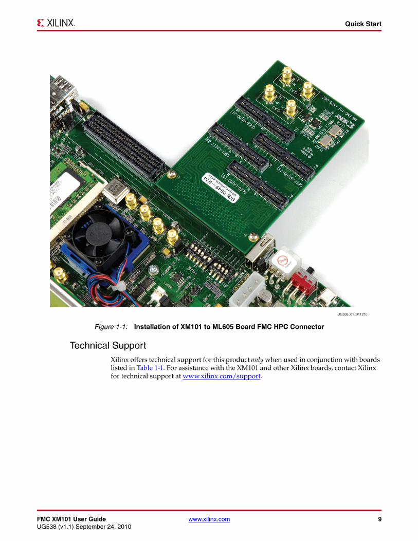
4. Install the XM101 to the ML605 FMC HPC connector J64. The XM101 hangs off the edge of the ML605 board as shown in Figure 1-1, page 9.
5. Turn the ML605 and attached XM101 board over such that the ML605 FPGA is facing the table. Install two screws from the bottom side of ML605 board's FMC HPC mounting holes into the two standoffs attached to the XM101. Hand tighten the two mounting screws to the bottom of the board.
6. Turn the ML605 and attached XM101 boards over such that the Xilinx FPGA is visible.
7. Connect the input power source to the ML605 board. Turn the ML605 board power input switch to ON.
The system is now ready for use.
FMC XM101 User Guide www.xilinx.com 9UG538 (v1.1) September 24, 2010
Quick Start
Technical SupportXilinx offers technical support for this product only when used in conjunction with boards listed in Table 1-1. For assistance with the XM101 and other Xilinx boards, contact Xilinx for technical support at www.xilinx.com/support.
X-Ref Target - Figure 1-1
Figure 1-1: Installation of XM101 to ML605 Board FMC HPC Connector
UG538_01_011210
10 www.xilinx.com FMC XM101 User GuideUG538 (v1.1) September 24, 2010
Chapter 1: XM101
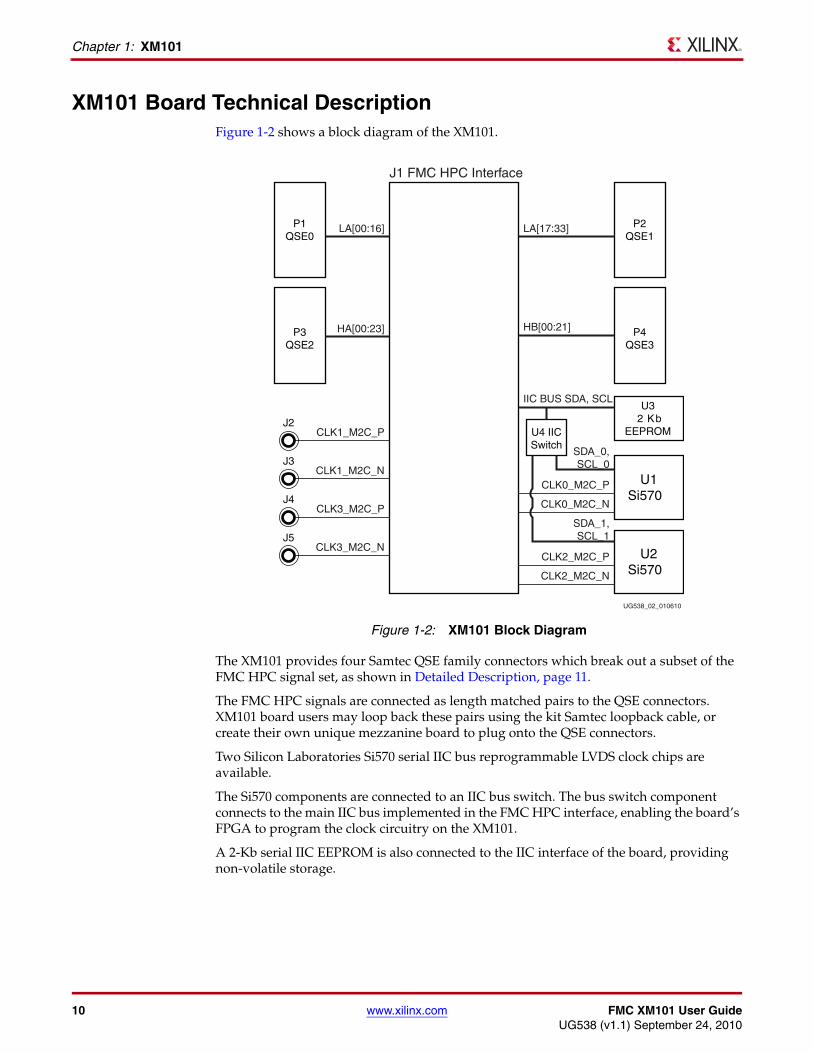
XM101 Board Technical DescriptionFigure 1-2 shows a block diagram of the XM101.
The XM101 provides four Samtec QSE family connectors which break out a subset of the FMC HPC signal set, as shown in Detailed Description, page 11.
The FMC HPC signals are connected as length matched pairs to the QSE connectors. XM101 board users may loop back these pairs using the kit Samtec loopback cable, or create their own unique mezzanine board to plug onto the QSE connectors.
Two Silicon Laboratories Si570 serial IIC bus reprogrammable LVDS clock chips are available.
The Si570 components are connected to an IIC bus switch. The bus switch component connects to the main IIC bus implemented in the FMC HPC interface, enabling the board’s FPGA to program the clock circuitry on the XM101.
A 2-Kb serial IIC EEPROM is also connected to the IIC interface of the board, providing non-volatile storage.
X-Ref Target - Figure 1-2
Figure 1-2: XM101 Block Diagram
U3 2 Kb
EEPROM
U1Si570
U2Si570
U4 IICSwitch
LA[00:16]
HA[00:23]
CLK1_M2C_P
J1 FMC HPC Interface
P1QSE0
P3QSE2
J2
LA[17:33]
HB[00:21]
P2QSE1
P4QSE3
CLK1_M2C_NJ3
CLK3_M2C_PJ4
CLK3_M2C_NJ5
CLK2_M2C_N
CLK2_M2C_P
CLK0_M2C_N
CLK0_M2C_P
IIC BUS SDA, SCL
SDA_0,SCL_0
SDA_1,SCL_1
UG538_02_010610
FMC XM101 User Guide www.xilinx.com 11UG538 (v1.1) September 24, 2010
XM101 Board Technical Description
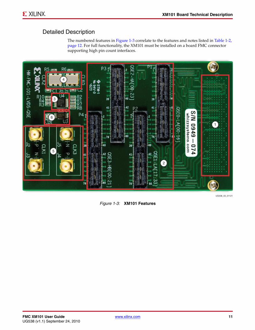
Detailed DescriptionThe numbered features in Figure 1-3 correlate to the features and notes listed in Table 1-2, page 12. For full functionality, the XM101 must be installed on a board FMC connector supporting high pin count interfaces.
X-Ref Target - Figure 1-3
Figure 1-3: XM101 Features
UG538_03_011210
1
2
3
6
4
5
12 www.xilinx.com FMC XM101 User GuideUG538 (v1.1) September 24, 2010
Chapter 1: XM101
Table 1-2: XM101 Features
Number Feature NotesSchematic
Page
1VITA 57.1 FMC HPC connector
J1: 80 signal pairs comprised of LA[00:33], HA[00:23] and HB[00:21], four clock pairs, and the IIC bus SDA, SCL. The connector is mounted on the bottom side of the card.
3 - 6
2 Samtec QSE Connectors
P1-P4: 4 Samtec QSE connectors with length-matched signal pairs wired to the FMC HPC connector as follows: P1 QSE0 LA[00:16], P2 QSE1 LA[17:33], P3 QSE2 HA[00:23], P4 QSE3 HB[00:21].
7
3PCA9543 IIC Bus Switch
U4: IIC bus switch is connected to the main FMC HPC IIC bus SDA and SCL signals. This component can switch its input IIC bus to one of two backside IIC bus connections. Each of the two Si570 clock chips resides on one of these backside IIC buses.
8
4
Silicon Labs Si570 Programmable XO/VCXO
U1, U2: Silicon Labs Si570 IIC serial bus programmable clock source devices with frequency range 10 MHz - 810 MHz. U1 drives signals CLK0_M2C_P/N; U2 drives CLK2_M2C_P/N
8
5 SMA Clock Connections
SMA pair J2 and J3 are connected to CLK1_M2C_P and N, respectively; SMA pair J4 and J5 are connected to CLK3_M2C_P and N, respectively.
8
6M24C02 2Kb IIC EEPROM
U3: IIC compatible electrically erasable programmable memory (EEPROM) with 2 Kb (256 bytes) of non-volatile storage.
8
FMC XM101 User Guide www.xilinx.com 13UG538 (v1.1) September 24, 2010
XM101 Board Technical Description
1. VITA 57.1 FMC HPC Connector J1
This connector interfaces to the board containing the Xilinx FPGA and mating FMC connector. The XM101 uses Samtec FMC HPC connector part number ASP-134488-01.
See Xilinx board user guides and schematics for a description of features provided by HPC interfaces contained on the board, including power supply specifications, FPGA banking connectivity, and FPGA pin assignments.
• For ML605 LPC and HPC interfaces, see UG534 ML605 Hardware User Guide
See the VITA57.1 Specification at www.vita.com/fmc.html for additional information on FMC.
2. Samtec QSE Connectors
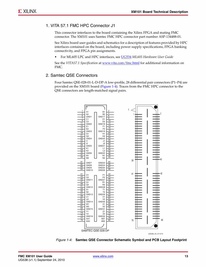
Four Samtec QSE-028-01-L-D-DP-A low-profile, 28 differential pair connectors (P1–P4) are provided on the XM101 board (Figure 1-4). Traces from the FMC HPC connector to the QSE connectors are length-matched signal pairs.X-Ref Target - Figure 1-4
Figure 1-4: Samtec QSE Connector Schematic Symbol and PCB Layout Footprint
1
1
2
39 40
41 42
79 80
SAMTEC-QSE-028-DP
A1A2
AA1AA2
AB1AB2
B1B2
C1C2
D1D2
E1E2
F1F2
G1G2
GND1
GND10
GND11
GND12
GND13
GND14
GND15
GND16
GND17
GND18
GND19
GND2
GND20
GND21
GND22
GND23GND24GND25GND26
GND27
GND28
GND29
GND3
GND30
GND31
GND32
GND4
GND5
GND6
GND7GND8GND9
H1H2
I1I2
J1J2
K1K2
L1L2
M1M2
N1N2
O1O2
P1P2
Q1Q2
R1R2
S1S2
T1T2
U1U2
V1V2
W1W2
X1X2
Y1Y2
Z1Z2
13
7779
7880
24
79
810
1315
1416
1921
5
84
45
51
57
63
69
75
6
12
18
11
24
30
36
85868788
46
52
58
17
64
70
76
23
29
35
818283
2022
2527
2628
3133
3234
3739
3840
4143
4244
4749
4850
5355
5456
5961
6062
6567
6668
7173
7274
UG538_04_011210
14 www.xilinx.com FMC XM101 User GuideUG538 (v1.1) September 24, 2010
Chapter 1: XM101
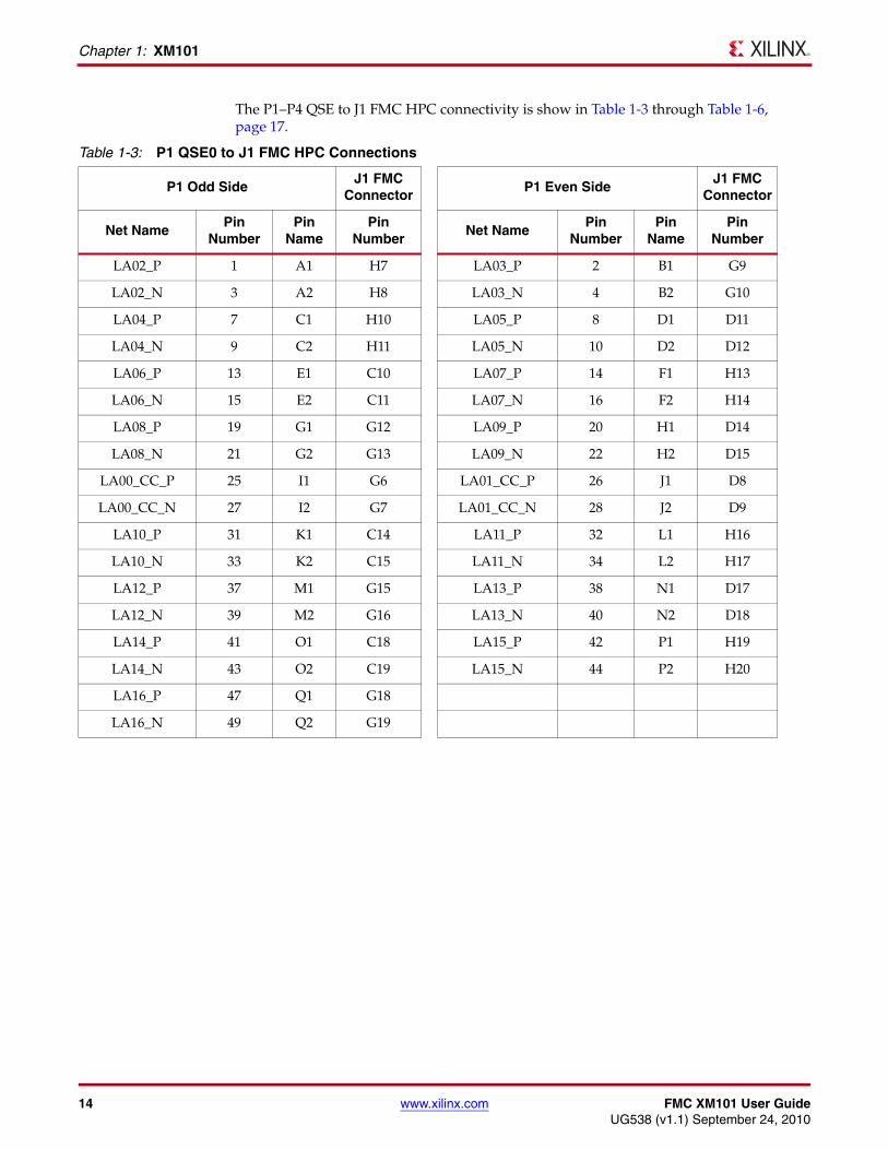
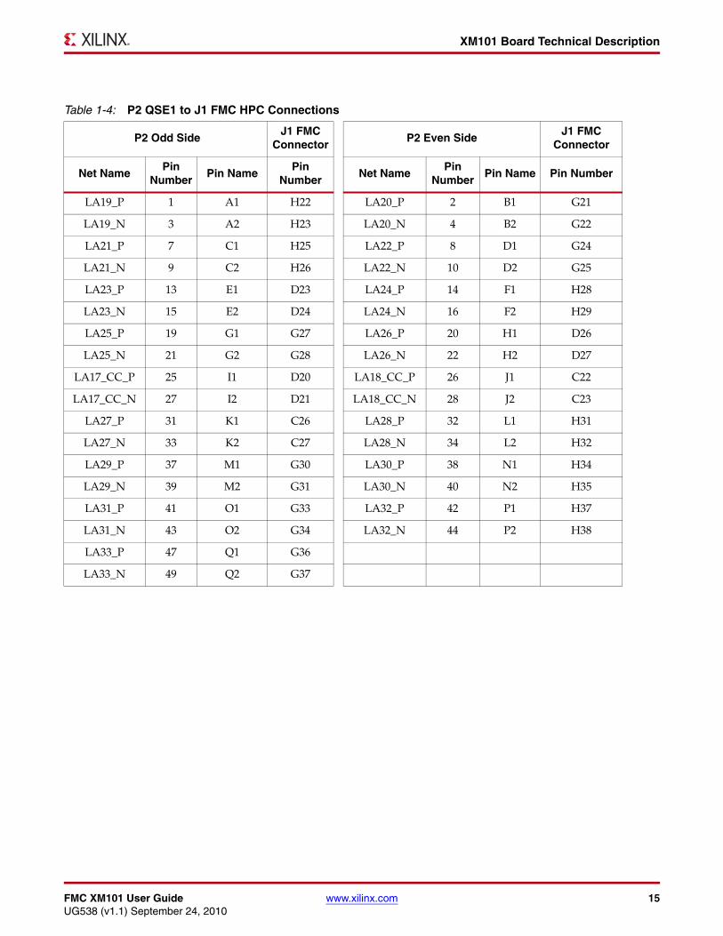
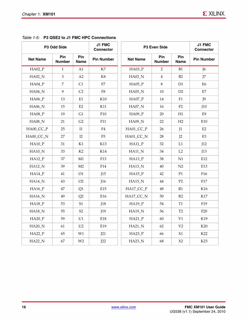
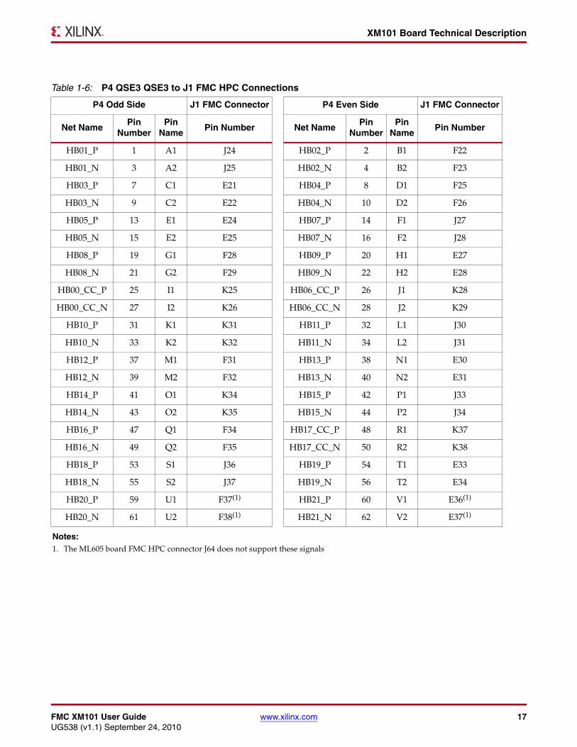
The P1–P4 QSE to J1 FMC HPC connectivity is show in Table 1-3 through Table 1-6, page 17.
Table 1-3: P1 QSE0 to J1 FMC HPC Connections
P1 Odd SideJ1 FMC
Connector P1 Even Side
J1 FMC Connector
Net NamePin
NumberPin
NamePin
NumberNet Name
Pin Number
Pin Name
PinNumber
LA02_P 1 A1 H7 LA03_P 2 B1 G9
LA02_N 3 A2 H8 LA03_N 4 B2 G10
LA04_P 7 C1 H10 LA05_P 8 D1 D11
LA04_N 9 C2 H11 LA05_N 10 D2 D12
LA06_P 13 E1 C10 LA07_P 14 F1 H13
LA06_N 15 E2 C11 LA07_N 16 F2 H14
LA08_P 19 G1 G12 LA09_P 20 H1 D14
LA08_N 21 G2 G13 LA09_N 22 H2 D15
LA00_CC_P 25 I1 G6 LA01_CC_P 26 J1 D8
LA00_CC_N 27 I2 G7 LA01_CC_N 28 J2 D9
LA10_P 31 K1 C14 LA11_P 32 L1 H16
LA10_N 33 K2 C15 LA11_N 34 L2 H17
LA12_P 37 M1 G15 LA13_P 38 N1 D17
LA12_N 39 M2 G16 LA13_N 40 N2 D18
LA14_P 41 O1 C18 LA15_P 42 P1 H19
LA14_N 43 O2 C19 LA15_N 44 P2 H20
LA16_P 47 Q1 G18
LA16_N 49 Q2 G19
FMC XM101 User Guide www.xilinx.com 15UG538 (v1.1) September 24, 2010
XM101 Board Technical Description
Table 1-4: P2 QSE1 to J1 FMC HPC Connections
P2 Odd SideJ1 FMC
Connector P2 Even Side
J1 FMC Connector
Net NamePin
NumberPin Name
Pin Number
Net NamePin
NumberPin Name Pin Number
LA19_P 1 A1 H22 LA20_P 2 B1 G21
LA19_N 3 A2 H23 LA20_N 4 B2 G22
LA21_P 7 C1 H25 LA22_P 8 D1 G24
LA21_N 9 C2 H26 LA22_N 10 D2 G25
LA23_P 13 E1 D23 LA24_P 14 F1 H28
LA23_N 15 E2 D24 LA24_N 16 F2 H29
LA25_P 19 G1 G27 LA26_P 20 H1 D26
LA25_N 21 G2 G28 LA26_N 22 H2 D27
LA17_CC_P 25 I1 D20 LA18_CC_P 26 J1 C22
LA17_CC_N 27 I2 D21 LA18_CC_N 28 J2 C23
LA27_P 31 K1 C26 LA28_P 32 L1 H31
LA27_N 33 K2 C27 LA28_N 34 L2 H32
LA29_P 37 M1 G30 LA30_P 38 N1 H34
LA29_N 39 M2 G31 LA30_N 40 N2 H35
LA31_P 41 O1 G33 LA32_P 42 P1 H37
LA31_N 43 O2 G34 LA32_N 44 P2 H38
LA33_P 47 Q1 G36
LA33_N 49 Q2 G37
16 www.xilinx.com FMC XM101 User GuideUG538 (v1.1) September 24, 2010
Chapter 1: XM101
Table 1-5: P3 QSE2 to J1 FMC HPC Connections
P3 Odd SideJ1 FMC
Connector P3 Even Side
J1 FMC Connector
Net NamePin
NumberPin
NamePin Number Net Name
Pin Number
Pin Name
Pin Number
HA02_P 1 A1 K7 HA03_P 2 B1 J6
HA02_N 3 A2 K8 HA03_N 4 B2 J7
HA04_P 7 C1 F7 HA05_P 8 D1 E6
HA04_N 9 C2 F8 HA05_N 10 D2 E7
HA06_P 13 E1 K10 HA07_P 14 F1 J9
HA06_N 15 E2 K11 HA07_N 16 F2 J10
HA08_P 19 G1 F10 HA09_P 20 H1 E9
HA08_N 21 G2 F11 HA09_N 22 H2 E10
HA00_CC_P 25 I1 F4 HA01_CC_P 26 J1 E2
HA00_CC_N 27 I2 F5 HA01_CC_N 28 J2 E3
HA10_P 31 K1 K13 HA11_P 32 L1 J12
HA10_N 33 K2 K14 HA11_N 34 L2 J13
HA12_P 37 M1 F13 HA13_P 38 N1 E12
HA12_N 39 M2 F14 HA13_N 40 N2 E13
HA14_P 41 O1 J15 HA15_P 42 P1 F16
HA14_N 43 O2 J16 HA15_N 44 P2 F17
HA16_P 47 Q1 E15 HA17_CC_P 48 R1 K16
HA16_N 49 Q2 E16 HA17_CC_N 50 R2 K17
HA18_P 53 S1 J18 HA19_P 54 T1 F19
HA18_N 55 S2 J19 HA19_N 56 T2 F20
HA20_P 59 U1 E18 HA21_P 60 V1 K19
HA20_N 61 U2 E19 HA21_N 62 V2 K20
HA22_P 65 W1 J21 HA23_P 66 X1 K22
HA22_N 67 W2 J22 HA23_N 68 X2 K23
FMC XM101 User Guide www.xilinx.com 17UG538 (v1.1) September 24, 2010
XM101 Board Technical Description
Table 1-6: P4 QSE3 QSE3 to J1 FMC HPC Connections
P4 Odd Side J1 FMC Connector P4 Even Side J1 FMC Connector
Net NamePin
NumberPin
NamePin Number Net Name
Pin Number
Pin Name
Pin Number
HB01_P 1 A1 J24 HB02_P 2 B1 F22
HB01_N 3 A2 J25 HB02_N 4 B2 F23
HB03_P 7 C1 E21 HB04_P 8 D1 F25
HB03_N 9 C2 E22 HB04_N 10 D2 F26
HB05_P 13 E1 E24 HB07_P 14 F1 J27
HB05_N 15 E2 E25 HB07_N 16 F2 J28
HB08_P 19 G1 F28 HB09_P 20 H1 E27
HB08_N 21 G2 F29 HB09_N 22 H2 E28
HB00_CC_P 25 I1 K25 HB06_CC_P 26 J1 K28
HB00_CC_N 27 I2 K26 HB06_CC_N 28 J2 K29
HB10_P 31 K1 K31 HB11_P 32 L1 J30
HB10_N 33 K2 K32 HB11_N 34 L2 J31
HB12_P 37 M1 F31 HB13_P 38 N1 E30
HB12_N 39 M2 F32 HB13_N 40 N2 E31
HB14_P 41 O1 K34 HB15_P 42 P1 J33
HB14_N 43 O2 K35 HB15_N 44 P2 J34
HB16_P 47 Q1 F34 HB17_CC_P 48 R1 K37
HB16_N 49 Q2 F35 HB17_CC_N 50 R2 K38
HB18_P 53 S1 J36 HB19_P 54 T1 E33
HB18_N 55 S2 J37 HB19_N 56 T2 E34
HB20_P 59 U1 F37(1) HB21_P 60 V1 E36(1)
HB20_N 61 U2 F38(1) HB21_N 62 V2 E37(1)
Notes: 1. The ML605 board FMC HPC connector J64 does not support these signals
18 www.xilinx.com FMC XM101 User GuideUG538 (v1.1) September 24, 2010
Chapter 1: XM101
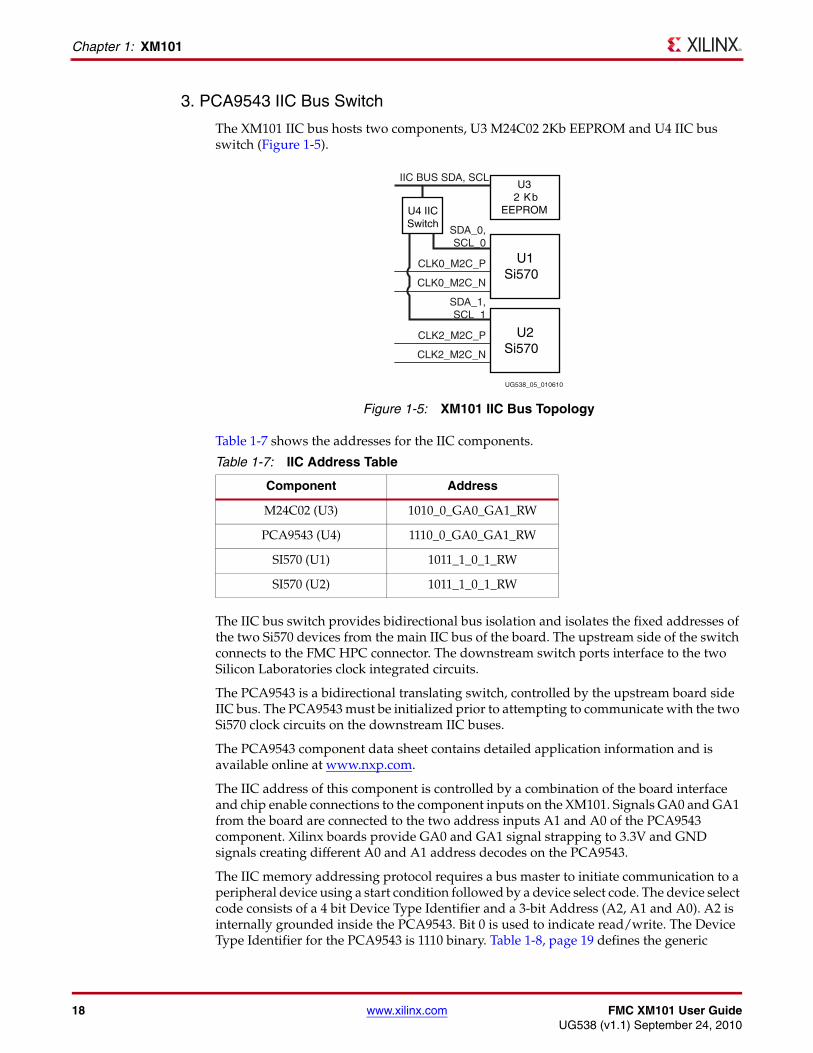
3. PCA9543 IIC Bus Switch
The XM101 IIC bus hosts two components, U3 M24C02 2Kb EEPROM and U4 IIC bus switch (Figure 1-5).
Table 1-7 shows the addresses for the IIC components.
The IIC bus switch provides bidirectional bus isolation and isolates the fixed addresses of the two Si570 devices from the main IIC bus of the board. The upstream side of the switch connects to the FMC HPC connector. The downstream switch ports interface to the two Silicon Laboratories clock integrated circuits.
The PCA9543 is a bidirectional translating switch, controlled by the upstream board side IIC bus. The PCA9543 must be initialized prior to attempting to communicate with the two Si570 clock circuits on the downstream IIC buses.
The PCA9543 component data sheet contains detailed application information and is available online at www.nxp.com.
The IIC address of this component is controlled by a combination of the board interface and chip enable connections to the component inputs on the XM101. Signals GA0 and GA1 from the board are connected to the two address inputs A1 and A0 of the PCA9543 component. Xilinx boards provide GA0 and GA1 signal strapping to 3.3V and GND signals creating different A0 and A1 address decodes on the PCA9543.
The IIC memory addressing protocol requires a bus master to initiate communication to a peripheral device using a start condition followed by a device select code. The device select code consists of a 4 bit Device Type Identifier and a 3-bit Address (A2, A1 and A0). A2 is internally grounded inside the PCA9543. Bit 0 is used to indicate read/write. The Device Type Identifier for the PCA9543 is 1110 binary. Table 1-8, page 19 defines the generic
X-Ref Target - Figure 1-5
Figure 1-5: XM101 IIC Bus Topology
Table 1-7: IIC Address Table
Component Address
M24C02 (U3) 1010_0_GA0_GA1_RW
PCA9543 (U4) 1110_0_GA0_GA1_RW
SI570 (U1) 1011_1_0_1_RW
SI570 (U2) 1011_1_0_1_RW
U3 2 Kb
EEPROM
U1Si570
U2Si570
U4 IICSwitch
CLK2_M2C_N
CLK2_M2C_P
CLK0_M2C_N
CLK0_M2C_P
IIC BUS SDA, SCL
SDA_0,SCL_0
SDA_1,SCL_1
UG538_05_010610
FMC XM101 User Guide www.xilinx.com 19UG538 (v1.1) September 24, 2010
XM101 Board Technical Description
PCA9543 Device Select Code as well as specific Device Code Select address when the XM101 is connected to a Xilinx board as defined in Table 1-1, page 7.
The PCA9543 has a Control register which must be initialized by the IIC bus master to enable the channel 0 downstream IIC port. Channel 0 must be enabled prior to attempting to communicate with the two downstream programmable clock devices on the XM101.
After the IIC bus master enables PCA9543 channel 0 downstream IIC bus, the bus master can communicate directly with either Si570 component without further interaction with the Control register. The Control Register can be read by the IIC bus master. Table 11 defines the PCA9543 Control Register.
The two downstream IIC devices connected to the PCA9543 are at the same IIC address:
• Si570 U1 IIC address is at 0x5D, PCA9543 control register bits CR[1:0] = 01
• Si570 U2 IIC address is at 0x5D, PCA9543 control register bits CR[1:0] = 10
The U4 PCA9543 IIC bus switch to J1 FMC HPC connections are shown in Table 1-10.
Table 1-8: PCA9543 IIC Switch Device Select Code
Bit 7:4 Device Type Identifier
Bit 3 Bit 2 Bit 1 Bit 0 LSB
Description
1110 0 GA0 GA1 Read/WriteConnected to mezzanine FMC HPC interface
Table 1-9: PCA9543 Control Register
Bit 7:4 Bit 3:2 Bit 1 Bit 0
XXXX XXChannel 1 Enable(1)
Channel 0 Enable(2)
Notes: 1. Channel 1 must be set to a logic 1 state by IIC bus master prior to attempting to
communicate with the Si570 U2.2. Channel 0 must be set to a logic 1 state by IIC bus master prior to attempting to
communicate with the Si570 U1.
Table 1-10: IIC Bus Switch to J1 FMC HPC Connections
U4 PCA9543 IIC Bus Switch J1 FMC
Connector
Net Name Pin Number Pin Number
SDA U4.13 C31
SCL U4.12 C30
20 www.xilinx.com FMC XM101 User GuideUG538 (v1.1) September 24, 2010
Chapter 1: XM101
4. Silicon Labs Si570 Clock Sources
The Silicon Labs Si570 serial IIC bus programmable clock source provides a low-jitter clock with a user-programmable output frequency from 10 to 810 MHz.
U1 and U2 Si570 are located at IIC address 0x5D and are accessed through the U4 PCA9543 IIC bus switch as described in 3. PCA9543 IIC Bus Switch.
U1 and U2 Si570 components are factory programmed with parameters in Table 1-11.
For additional information on this component, including reprogramming the clock frequency through the IIC serial bus interface, consult the manufacturer's data sheet at: www.silabs.com.
The U1 and U2 Si570 output clocks to J1 FMC HPC connections are shown in Table 1-12.
Table 1-11: Characteristics of Si570 Component
Si570 Characteristic XM101
Output Format LVDS
Output Enable Polarity High
Temperature Stability 50 ppm
Frequency Range 10–810 MHz
Six-Digit Startup Frequency 156.250 MHz
Power Supply 3.3V
IIC Address x5D
Table 1-12: Si570 to FMC HPC Connections
Si570J1 FMC
Connector
Net Name Pin Number Pin Number
CLK0_M2C_P U1.4 H4
CLK0_M2C_N U1.5 H5
CLK2_M2C_P U2.4 K4
CLK2_M2C_N U2.5 K5
FMC XM101 User Guide www.xilinx.com 21UG538 (v1.1) September 24, 2010
XM101 Board Technical Description
5. SMA Clock Connections
Four SMA connectors (J2 - J5) are provided on the XM101 board.
The SMA to J1 FMC HPC connections are shown in Table 1-13.
6. M24C02 2 Kb IIC EEPROM
An STMicroelectronics M24C02 2 Kb serial IIC bus EEPROM (U3) component provides a small amount of non-volatile memory storage on the XM101. The IIC interface is connected directly to the board's IIC interface as shown in Figure 1-2, page 10.
The IIC address of this component is controlled by a combination of the board's interface and chip enable connections to the component inputs on the XM101. Signals GA0 and GA1 from the board are connected to the chip enable inputs of the M24C02 component enables E0 and E1. Xilinx boards provide GA0 and GA1 signal strapping to 3.3V and GND signals creating different E0 and E1 chip enable decodes on the E1 and E0 inputs of the EEPROM.
The IIC memory addressing protocol requires a bus master to initiate communication to a peripheral device using a start condition followed by a device select code. The device select code consists of a 4 bit Device Type Identifier and a 3-bit Chip Enable Address (E2, E1 and E0). Bit 0 is used to indicate read/write. The Device Type Identifier for the EEPROM is 1010 binary. Table 1-14 defines the generic EEPROM Device Select Code as well as specific Device Code Select addresses of the EEPROM when the XM101 is connected to a Xilinx board defined in Table 1-1, page 7.
The M24C02 component data sheet is available online at www.st.com.
Table 1-13: SMA to FMC HPC Connections
SMAJ1 FMC
Connector
Net Name Pin Number Pin Number
CLK1_M2C_P J2.1 G2
CLK1_M2C_N J3.1 G3
CLK3_M2C_P J4.1 J2
CLK3_M2C_N J5.1 J3
Table 1-14: EEPROM IIC Device Select Code
Bit 7:4 Device Type Identifier
Bit 3 Bit 2 Bit 1 Bit 0 LSB Description
1010 0 GA0 GA1 Read/WriteConnected to mezzanine FMC HPC interface
22 www.xilinx.com FMC XM101 User GuideUG538 (v1.1) September 24, 2010
Chapter 1: XM101