a study on anisotropic etching of (100) silicon in aqueous koh solution
TRANSCRIPT
Int. J. Chem. Sci.: 6(3), 2008, 1168-1176
A STUDY ON ANISOTROPIC ETCHING OF (100) SILICON
IN AQUEOUS KOH SOLUTION
P. A. ALVI∗∗∗∗,V. S. MEEL
a, K. SARITA
b, J. AKHTAR
c,
K. M. LAL, A. AZAM and S. A. H. NAQVI
Department of Applied Physics, Z. H. College of Engineering and Technology,
Aligarh Muslim University, ALIGARH-202002 (U. P.) INDIA aDepartment of Computer Science and Electronics, Jaipur National University, JAIPUR (Raj.) INDIA
bDepartmant of Physics, Banasthali Uniersity, BANASTHALI (Raj.) INDIA
cMicroelectronics Technology Group, Semiconductor Devices Area, Central Electronics Engineering
Research Institute, PILANI-333031 (Raj.) INDIA
ABSTRACT
This paper reports the temperature and concentration dependence of anisotropic etching of
(100) silicon in aqueous KOH solution. Etching rate of wet etching of (100) silicon in pure KOH
solution has been experimentally determined with varying KOH concentration and the temperature of
the KOH solution. Atomic force microscopy (AFM) and optical microscopy have been employed for the
inspection of the quality of the etched surfaces. It has been observed that the etching rate increases with
increasing temperature of the KOH solution for concentrations varying from 10% to 45% by weight.
However, for a given KOH temperature, the etching rate decreases with increasing KOH concentration.
The 10% KOH solution in contrary enhances oxidation of the silicon surfaces leading towards more
hydrophilic and therefore a reduced etching rate is resulted.
Key words: MEMS, Anisotropic etching, LPCVD, KOH
INTRODUCTION
Anisotropic etching of silicon refers to the direction-dependent etching of silicon,
usually by alkaline etchants like aqueous KOH, TMAH and other alkaline hydroxides like
NaOH and LiOH. Due to the strong dependence of the etch rate on crystal direction and on
etchant concentration, a large variety of silicon structures can be fabricated in a highly
controllable and reproducible manner. Hence, anisotropic etching of (100) silicon has been
a key process in common MEMS based technologies for realizing 3-D structures. These
structures include V-grooves for VMOS transistors, small holes for ink jets and
∗ Author for correspondence; E-mail : [email protected]

Int. J. Chem. Sci.: 6(3), 2008
1169
diaphragms for MEMS pressure sensors1. The actual reaction mechanism has not been
fully understood for a long and a comprehensive physical model for the process has not yet
been developed. With increasing numbers of MEMS applications, interest has grown for
process modelling, simulation and software tools useful for prediction of etched surface
profile.
Chemical etching of silicon depends on crystal orientation, temperature and
concentration of the etchant. Geometry of the area to be etched also influences the etch rate
owing to the different crystal planes encountered during the etching process. In order to
minimize the influence of other chemicals on the etching mechanism and therefore, to
obtain more accurate results, pure KOH solution has been preferred over a number of
mixtures with moderators like ethylene diamine pyrocatechol (EDP) and isopropyl alcohol
(IPA). This has resulted into increasing the temperature of the solution up to its boiling
point. Anisotropic etching of silicon has been carried out at temperature near boiling point
with smooth surface2. 6-8 times faster etching rate has been obtained with reasonable good
etched surface quality. The chemical etching mechanism of silicon in KOH is still under
debate and therefore, more experimental results under varying conditions are required for
preparing accurate physical models. During silicon etching in KOH solution, H2 bubbles
are generated and to a large extent the quality of the etched surface depends on the rate at
which these bubbles are removed from the etched silicon surface. Various techniques have
been introduced for removing these bubbles during the etching process3-6. In the chemical
process of anisotropic etching of silicon, surface of the silicon plane undergoes through the
stages of hydrophobic to hydrophilic. The formation of large hydrogen gas bubbles
depends on the adhesion between the KOH solution and the silicon wafer. If the surface is
hydrophilic, only small bubbles are formed and roughness is reduced and if the surface is
hydrophobic, large bubbles are formed and hence large hillocks are formed. Concentrated
KOH solutions tend to adhere more to silicon surfaces, resulting in smaller bubbles and
less roughness. These bubbles cause temporary localized etch stops equivalent to etch
masks. The etching rate and the quality of the etched surface have been studied
experimentally in the present work. Relevant details of the experiment and the results have
been presented in the following sections.
EXPERIMENTAL
Silicon (100) samples were prepared starting with device grade chemical cleaning
of the wafer. Thermal oxidation of 0.5-micrometer thickness was grown using wet-dry-wet
sequence at 1100 °C, in a horizontal quartz furnace. LPCVD silicon nitride was deposited
P. A. Alvi et al.: A Study on Anisotropic….
1170
over that layer, at 780 °C for a thickness of 0.15 micrometer in a horizontal quartz furnace
reactor. The combination of silicon dioxide and silicon nitride provides stable masking
action in KOH solution at elevated temperatures. Square windows of 2.0 mm size were
delineated in an array using photolithography. Dry etching was used to selectively remove
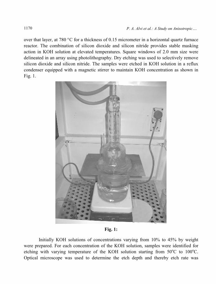
silicon dioxide and silicon nitride. The samples were etched in KOH solution in a reflux
condenser equipped with a magnetic stirrer to maintain KOH concentration as shown in
Fig. 1.
Fig. 1:
Initially KOH solutions of concentrations varying from 10% to 45% by weight
were prepared. For each concentration of the KOH solution, samples were identified for
etching with varying temperature of the KOH solution starting from 50oC to 100oC.
Optical microscope was used to determine the etch depth and thereby etch rate was
Int. J. Chem. Sci.: 6(3), 2008
1171
calculated for each sample. Quality of the etched surfaces was inspected using AFM in
contact mode.
RESULTS AND DISCUSSION
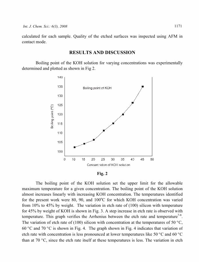
Boiling point of the KOH solution for varying concentrations was experimentally
determined and plotted as shown in Fig 2.
Fig. 2
The boiling point of the KOH solution set the upper limit for the allowable
maximum temperature for a given concentration. The boiling point of the KOH solution
almost increases linearly with increasing KOH concentration. The temperatures identified
for the present work were 80, 90, and 100oC for which KOH concentration was varied
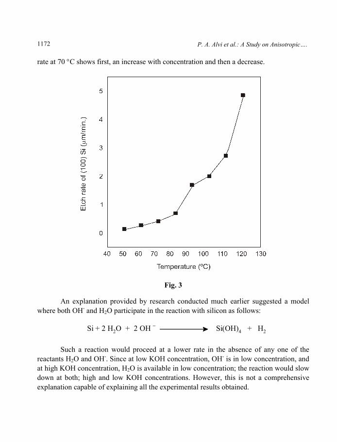
from 10% to 45% by weight. The variation in etch rate of (100) silicon with temperature
for 45% by weight of KOH is shown in Fig. 3. A step increase in etch rate is observed with
temperature. This graph verifies the Arrhenius between the etch rate and temperature7-8.
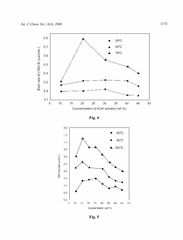
The variation of etch rate of (100) silicon with concentration at the temperatures of 50 °C,
60 °C and 70 °C is shown in Fig. 4. The graph shown in Fig. 4 indicates that variation of
etch rate with concentration is less pronounced at lower temperatures like 50 °C and 60 °C
than at 70 °C, since the etch rate itself at these temperatures is less. The variation in etch
P. A. Alvi et al.: A Study on Anisotropic….
1172
rate at 70 °C shows first, an increase with concentration and then a decrease.
Fig. 3
An explanation provided by research conducted much earlier suggested a model
where both OH- and H2O participate in the reaction with silicon as follows:
Si + 2 H2O + 2 OH
− Si(OH)4 + H2
Such a reaction would proceed at a lower rate in the absence of any one of the
reactants H2O and OH-. Since at low KOH concentration, OH- is in low concentration, and
at high KOH concentration, H2O is available in low concentration; the reaction would slow
down at both; high and low KOH concentrations. However, this is not a comprehensive
explanation capable of explaining all the experimental results obtained.
Int. J. Chem. Sci.: 6(3), 2008
1173
Fig. 4
Fig. 5
P. A. Alvi et al.: A Study on Anisotropic….
1174
Fig. 5 shows the result obtained for the variation of etch rate of (100) silicon with
concentration at the temperatures of 80 °C, 90 °C and 100 °C. The etching rate shows a peak for each temperature curve that is observed at lower concentration with increasing
temperature. At 80 0C, a maximum etching rate of 1.5 µm/min is obtained for 25 wt %
KOH solution. For temperatures above 800C, the peak of the maximum etch rate is
observed at 15 wt % KOH solution. At 100 0C the maximum etch rate is about 3 times of
that at 80 0C.
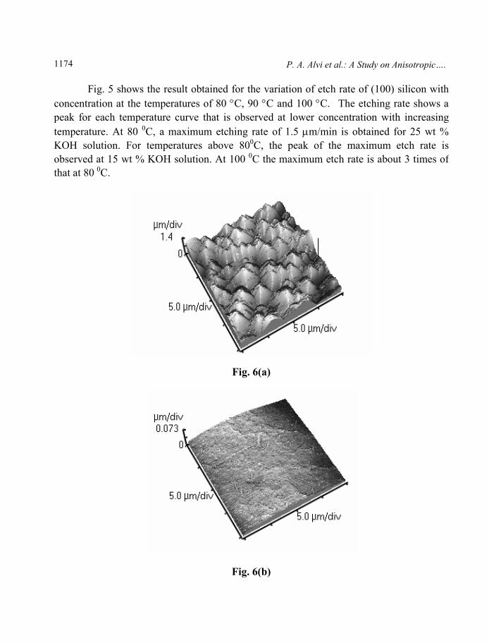
Fig. 6(a)
Fig. 6(b)

Int. J. Chem. Sci.: 6(3), 2008
1175
The morphology of the etched surface obtained with an AFM and optical
microscope at typically two concentrations of the KOH solutions has been shown in Fig. 6
and 7. In 10% wt KOH solution, surface of the silicon becomes more hydrophilic, which
further reduces to less hydrophilic with increasing temperature. The silicon (100) surface is
subjected to changes from hydrophilic to hydrophobic and again hydrophilic with
increasing KOH concentration. However, the higher temperature has been found to be
preferred one with low KOH concentration.
Fig.7 (a)
Fig. 7 (b)
CONCLUSION
Faster etching rate with smooth silicon surface has been observed at higher
P. A. Alvi et al.: A Study on Anisotropic….
1176
temperature in low KOH concentration solutions. The data has been found useful to
formulate a physical model for the anisotropic etching of (100) silicon in KOH solution.
The boiling point of the KOH solution decreases with decreasing concentration and
thereby limits the use of higher temperature at low concentration KOH solutions.
However, 100 oC is the most preferred temperature for 15% wt KOH solution for smooth
etched surface and faster etching rate. At higher temperature of the KOH solution,
hydrophobic nature of silicon surface tends to prevail giving rise the enhanced etched rate
with smooth silicon surface. Pure KOH solution provides improved process control
resulting into added advantage for MEMS applications.
ACKNOWLEDGEMENT
Authors thankfully acknowledge Dr Chandra Shekhar, Director, CEERI, Pilani
(Rajasthan) for providing laboratory facilities in his institute.
REFERENCES
1. P. A. Alvi, B. D. Lourembam, V. P. Deshwal, B. C. Joshi and J. Akhtar, Sensor
Review, 26 3, 179-185 (2006).
2. H. Tanaka, S. Yamashita, Y. Abe, M. Shikida, K. Sato, Sensors and Actuators A114
516-520 (2004).
3. Theo Baum and David J. Schiffin, J. Micromech. Microeng., 7, 338-342 (1997).
4. H. Schröder, E. Obermeier and A. Steckenborn, Micropyramidal Hillocks on KOH
Etched {100} Silicon Surfaces, Formation, Prevention and Removal, J. Micromech.
Microeng. 9, 139-145 (1999).
5. Jiang, Yanfeng and Qing-an Huang, A Physical Model for Silicon Anisotropic
Chemical Etching, Institute of Physics Publishing, Semiconductor Science &
Technology, 20, 524–531 (2005).
6. Information on http, //www-mat. ee. tu-berlin. de/papers/public99/Schr1. html
7. H. Seidel et al, Anisotropic Etching of Crystalline Silicon in Alkaline Solution, J.
Electrochem. Soc. 137, 11, (1990).
8. M. Jan Lysko, Anisotropic Etching of the Silicon Crystal – Surface Free Energy
Model, Mater. Sci. in Semiconductor Processing, 6, 235-241(2003).
Accepted : 26.05.2008