article in press - keio university · mechanism for material removal in diamond turning of...
TRANSCRIPT
ARTICLE IN PRESS
International Journal of Machine Tools & Manufacture 49 (2009) 366–374
Contents lists available at ScienceDirect
International Journal of Machine Tools & Manufacture
0890-69
doi:10.1
� Corr
E-m
journal homepage: www.elsevier.com/locate/ijmactool
Mechanism for material removal in diamond turning of reaction-bondedsilicon carbide
Jiwang Yan �, Zhiyu Zhang, Tsunemoto Kuriyagawa
Department of Nanomechanics, Graduate School of Engineering, Tohoku University, Aoba 6-6-01, Aramaki, Aoba-ku, Sendai 980-8579, Japan
a r t i c l e i n f o
Article history:
Received 7 October 2008
Received in revised form
16 December 2008
Accepted 18 December 2008Available online 1 January 2009
Keywords:
Silicon carbide
Ductile machining
Diamond turning
Phase transformation
Chip formation
Tool wear
55/$ - see front matter & 2009 Elsevier Ltd. A
016/j.ijmachtools.2008.12.007
esponding author. Tel.: +8122 795 6946; fax:
ail address: [email protected] (J.
a b s t r a c t
Reaction-bonded silicon carbide (RB-SiC) is a new ceramic material that has extremely high strength
and hardness. Diamond turning experiments were performed on RB-SiC to investigate the microscopic
material removal mechanism. Diamond tools with large nose radii of 10 mm were used for machining. It
was found that the surface roughness was not significantly affected by the tool feed rate, but was
strongly dependent on the tool rake angle. The mechanism for material removal involved plastic
deformation, microfracture and dislodgement of 6H-SiC grains. Raman spectroscopy revealed that the
silicon bond component underwent amorphization, while no phase transformation of 6H-SiC grains was
observed. Tool wear was also investigated and two types of wear patterns were identified. Under the
experimental conditions used, a surface finish of 23 nm Ra was obtained even at an extremely high tool
feed rate of 72mm/rev. This study demonstrates the feasibility of precision machining of RB-SiC by
diamond turning at a very high material removal rate.
& 2009 Elsevier Ltd. All rights reserved.
1. Introduction
Silicon carbide (SiC) is an important ceramic material that hasbeen extensively used in high-temperature and/or high-pressureapplications. For example, in the optical manufacturing industry,SiC is an excellent material for molding dies used for hot-pressmolding of aspherical glass lenses [1], due to material propertiessuch as high-temperature hardness, thermal shock resistance andchemical stability, which are superior to those of other materials.
The mechanical, thermal and chemical properties of SiC aredistinctly dependent on the material manufacturing method.Conventional methods for the manufacture of SiC include pressure-less sintering, gas pressure sintering and hot pressing, where SiCgrains are bonded together by a variety of other materials, e.g.boron (B), carbon (C) and aluminum (Al). As a new method,reaction bonding of SiC has become the focus of recent research.Reaction-bonded silicon carbide (RB-SiC) is fabricated by infiltrat-ing silicon (Si) melt into a green compact consisting of C and SiC(mostly 6H-SiC) powders. The liquid Si reacts with the C particles,forming new SiC particles. In this way, a very dense SiC body isproduced without the formation of micropores. However, theinfiltrated Si melt cannot react with C completely; therefore, excessSi remains in the body of material as a bonding component [2].
RB-SiC has been considered to be a most promising material ofthe SiC ceramics family. It can be manufactured at relatively low
ll rights reserved.
+8122 795 7027.
Yan).
temperatures and with low production costs. It has high purity,dense structure and excellent thermo-mechanical characteristics,such as high thermal stability and conductivity, high specific heatcapacity and low thermal expansion. In particular, RB-SiC ischaracterized by its low density (slightly higher than aluminum)and high stiffness (bending strength over 1000 GPa and Young’smodulus higher than 400 GPa). The unique properties of RB-SiCalso enable it to be used under cryogenic temperatures, forexample, as large-diameter light mirrors of infrared universeimaging systems used in space [3].
However, RB-SiC is typically a difficult material to machine.Recent efforts have focused on the precision machining of RB-SiCby grinding [4,5], lapping [6], polishing [7] and combinations ofthese. However, to date, there have been no reports on single-point machining (cutting) of RB-SiC. RB-SiC is harder than mostother materials except diamond, cubic boron nitride (cBN) andboron carbide (B4C) [8], and hence available cutting tool materialsfor machining RB-SiC are very limited. Investigation of themachinability of RB-SiC using ultra hard cutting tools is thereforea challenging issue. If successful methods for precision cutting ofRB-SiC can be developed, then extensive industrial applications ofRB-SiC can be expected. Compared with abrasive machiningprocesses, cutting has higher material removal rates and higherflexibility when fabricating complicated shapes and microstruc-tures.
The aim of the present work is to investigate the machinabilityof RB-SiC by precision cutting tests using a single-crystal diamondtool. The machining mechanisms were investigated with respectto surface topography, microstructural changes, chip formation
ARTICLE IN PRESS
Tool shank R
Rake face
J. Yan et al. / International Journal of Machine Tools & Manufacture 49 (2009) 366–374 367
and tool wear characteristics. Emphasis was placed on the effectsof tool feed rate and tool rake angle in this investigation. Thecutting phenomena observed for RB-SiC were also compared withour previous works on the precision machining of Si andgermanium (Ge). It is expected that the present study will providefeasible evidence for the partial or complete replacement ofabrasive machining processes with diamond turning in thefabrication of precision micro RB-SiC parts.
Rake face
Cutting edge R=10 mm
�
�
2. Experimental details
2.1. Machining apparatus
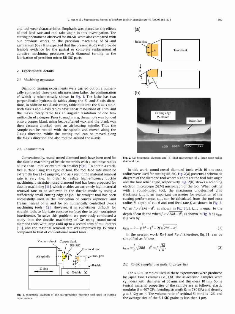
Diamond turning experiments were carried out on a numeri-cally controlled three-axis ultraprecision lathe, the configurationof which is schematically shown in Fig. 1. The lathe has twoperpendicular hydrostatic tables along the X- and Z-axis direc-tions, in addition to a B-axis rotary table built into the X-axis table.Both X-axis and Z-axis tables have linear resolutions of 1 nm, andthe B-axis rotary table has an angular resolution of one ten-millionths of a degree. Prior to machining, the sample was bondedonto a copper blank using heat-softened wax and the blank wasthen vacuum chucked onto an air-bearing spindle. Thus thesample can be rotated with the spindle and moved along theZ-axis direction, while the cutting tool can be moved alongthe X-axis direction and also rotated around the B-axis.
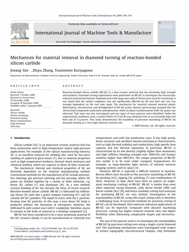
Fig. 2. (a) Schematic diagram and (b) SEM micrograph of a large nose-radius
diamond tool.
2.2. Diamond tool
Conventionally, round-nosed diamond tools have been used forthe ductile machining of brittle materials with a tool nose radiusof less than 1 mm, or even much smaller [9,10]. To obtain a crack-free surface using this type of tool, the tool feed rate must beextremely low (1–3mm/rev), and as a result, the material removalrate is very low. In order to realize high-efficiency ductilemachining, a straight-nosed diamond tool has been proposed forductile machining [11], which enables an extremely high materialremoval rate to be achieved in the ductile mode by using asufficiently small cutting edge angle. The straight tool has beensuccessfully used in the fabrication of convex aspherical andFresnel lenses of Si and Ge on numerically controlled 3-axismachining tools [12]. However, it is sometimes difficult forstraight tools to fabricate concave surfaces due to tool–workpieceinterference. To solve this problem, we previously conducted astudy into the ductile machining of Ge using round-noseddiamond tools with large radii up to a several tens of millimeters[13], and the material removal rate was improved by 15 timescompared to that of conventional round tools.
Vacuum chuck Copper blankRB-SiC
Diamond tool
Z-ableX-table
B-table
Tool postAir spindle
Fig. 1. Schematic diagram of the ultraprecision machine tool used in cutting
experiments.
In this work, round-nosed diamond tools with 10 mm noseradius were used for cutting RB-SiC. Fig. 2(a) presents a schematicdiagram of the diamond tool where a and g are the tool rake angleand the tool relief angle, respectively. Fig. 2(b) shows a scanningelectron microscope (SEM) micrograph of the tool. When cuttingwith a round-nosed tool, the maximum undeformed chipthickness tmax is an important parameter for evaluation of thecutting performance. tmax can be calculated from the tool noseradius R, depth of cut d and tool feed rate f, as shown in Fig. 3.
When fXffiffiffiffiffiffiffiffiffiffiffiffiffiffiffiffiffiffiffiffi2Rd� d2
p, as shown in Fig. 3(a), tmax is equal to the
depth of cut d; and when foffiffiffiffiffiffiffiffiffiffiffiffiffiffiffiffiffiffiffiffi2Rd� d2
p, as shown in Fig. 3(b), tmax
is given by
tmax ¼ R�
ffiffiffiffiffiffiffiffiffiffiffiffiffiffiffiffiffiffiffiffiffiffiffiffiffiffiffiffiffiffiffiffiffiffiffiffiffiffiffiffiffiffiffiffiffiffiffiffiffiffiffiR2þ f 2� 2f
ffiffiffiffiffiffiffiffiffiffiffiffiffiffiffiffiffiffiffiffi2Rd� d2
qr. (1)
In the present work, Rbf and Rbd; therefore, Eq. (1) can besimplified as follows:
tmax �f
R
ffiffiffiffiffiffiffiffiffiffiffiffiffiffiffiffiffiffiffiffi2Rd� d2
q� f
ffiffiffiffiffiffi2d
R
r. (2)
2.3. RB-SiC samples and material properties
The RB-SiC samples used in these experiments were producedby Japan Fine Ceramics Co., Ltd. The as-received samples werecylinders with diameter of 30 mm and thickness 10 mm. Sometypical material properties of the sample are as follows: elasticmodulus E ¼ 407 GPa; bending strength RT ¼ 780 GPa and densityr ¼ 3.12 g cm�3. The volume ratio of residual Si bond is 12%, andthe average size of the 6H-SiC grains is less than 1mm.

ARTICLE IN PRESS
f
dtmax
R
R
f
d
Feed direction
Cutting direction
Fig. 3. Schematic model of the maximum undeformed chip thickness tmax for
cutting with a round-nosed tool when (a) fXffiffiffiffiffiffiffiffiffiffiffiffiffiffiffiffiffiffiffiffi2Rd� d2
pand (b) fo
ffiffiffiffiffiffiffiffiffiffiffiffiffiffiffiffiffiffiffiffi2Rd� d2
p.
SiC
Si
Fig. 4. (a) SEM micrograph of a FAB surface-etched RB-SiC sample. The smooth
region is SiC and the micropits correspond to the Si bond. (b) Schematic model of
the RB-SiC material microstructure.
Table 1Machining conditions.
Workpiece material RB-SiC
Tool material Single-crystal diamond
Tool radius R 10 mm
Rake angle a 01, �401
Relief angle g 101
Depth of cut d 2mm
Spindle speed v 2000 rpm
Tool feed rate f 0.1–72mm/rev
Maximum undeformed chip thickness tmax 2–1440 nm
Cutting environment Dry
J. Yan et al. / International Journal of Machine Tools & Manufacture 49 (2009) 366–374368
In order to clarify the microstructure, the surface of a samplewas etched for 15 min using a fast atom beam (FAB) source with SF6
as a process gas. Fig. 4(a) shows an SEM micrograph of the etched
surface. Since the etching rate of Si is much higher than that of SiC,the Si bond on the surface was etched deeper than SiC, resulting inthe formation of micropits. The SiC grains (smooth region) and Sibond (corresponding to the micropits) can be clearly identified inthe micrograph. The sizes of intergrain residual Si bond portions areless than 1mm, and most of the SiC grains are directly bonded toeach other without the presence of Si at the grain boundaries.Fig. 4(b) presents a schematic model of the RB-SiC microstructure.In the material, the newly reaction-generated SiC grains are closelycombined to the originally existing SiC grains, resulting in a verydense structure.
These results indicate that the microstructure of RB-SiC isdistinctly different from those of single-crystal SiC and SiCprepared by chemical vapor deposition (CVD). Single-crystal SiChas a uniform crystalline lattice structure across the entire wafer.CVD-SiC has polycrystalline or amorphous structure, dependingon the deposition conditions used. However, both single-crystalSiC and CVD-SiC are single-phase materials with extremely highpurity. Therefore, it can be presumed that the cutting mechanismof RB-SiC, which is a two-phase compound material having amajor phase of high hardness (SiC) and a minor phase of lowhardness (Si), will be distinctly different from those of single-crystal SiC wafer [14] and CVD-SiC [15]. It will be also differentfrom those of multi-phase materials such as particle-reinforcedmetal matrix composites (MMCs), which are composed of a majorphase of low-hardness matrix and a minor phase of reinforcingparticles embedded in the matrix [16–18].
2.4. Machining conditions and surface characterization methods
Face turning was performed on the end faces of the samples. Thedetailed machining conditions are listed in Table 1. After machining,the resulting workpiece surfaces were evaluated in terms of surfaceroughness/topography and material microstructural changes. Thesurface roughness was measured using a contact-type stylusprofilometer (Form Talysurf 6, Taylor Hobson), and the materialmicrostructural change was examined using a laser micro-Ramanspectrometer (NRS-2100, Jasco). The laser wavelength in the Ramansystem was 532 nm and the nominal spot size of the laser was 1mm.Samples of machined specimens were Au–Pd coated for 30 s and thesurface damage was examined using SEM. SEM observation of thecutting chips was also performed to assist clarification of thematerial removal mechanisms, and the cutting tools were alsoexamined to evaluate tool wear patterns.
3. Results and discussion
3.1. Effects of tool feed rate
Firstly, a tool with a 01 rake angle was used for cutting toexamine the effect of tmax on the surface roughness and the
ARTICLE IN PRESS
J. Yan et al. / International Journal of Machine Tools & Manufacture 49 (2009) 366–374 369
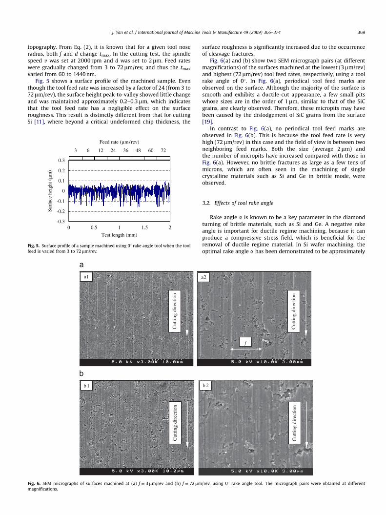
topography. From Eq. (2), it is known that for a given tool noseradius, both f and d change tmax. In the cutting test, the spindlespeed v was set at 2000 rpm and d was set to 2mm. Feed rateswere gradually changed from 3 to 72mm/rev, and thus the tmax
varied from 60 to 1440 nm.Fig. 5 shows a surface profile of the machined sample. Even
though the tool feed rate was increased by a factor of 24 (from 3 to72mm/rev), the surface height peak-to-valley showed little changeand was maintained approximately 0.2–0.3mm, which indicatesthat the tool feed rate has a negligible effect on the surfaceroughness. This result is distinctly different from that for cuttingSi [11], where beyond a critical undeformed chip thickness, the
-0.3
-0.2
-0.1
0
0.1
0.2
0.3
0
Test length (mm)
Surf
ace
heig
ht (µm
)
Feed rate (µm/rev)
3 726 12 36 48
0.5 1 1.5 2
24 60
Fig. 5. Surface profile of a sample machined using 01 rake angle tool when the tool
feed is varied from 3 to 72mm/rev.
Cut
ting
dire
ctio
n
a1
b 1
Cut
ting
dire
ctio
n
Fig. 6. SEM micrographs of surfaces machined at (a) f ¼ 3mm/rev and (b) f ¼ 72mm
magnifications.
surface roughness is significantly increased due to the occurrenceof cleavage fractures.
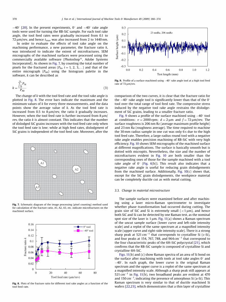
Fig. 6(a) and (b) show two SEM micrograph pairs (at differentmagnifications) of the surfaces machined at the lowest (3mm/rev)and highest (72mm/rev) tool feed rates, respectively, using a toolrake angle of 01. In Fig. 6(a), periodical tool feed marks areobserved on the surface. Although the majority of the surface issmooth and exhibits a ductile-cut appearance, a few small pitswhose sizes are in the order of 1mm, similar to that of the SiCgrains, are clearly observed. Therefore, these micropits may havebeen caused by the dislodgement of SiC grains from the surface[19].
In contrast to Fig. 6(a), no periodical tool feed marks areobserved in Fig. 6(b). This is because the tool feed rate is veryhigh (72mm/rev) in this case and the field of view is between twoneighboring feed marks. Both the size (average 2mm) andthe number of micropits have increased compared with those inFig. 6(a). However, no brittle fractures as large as a few tens ofmicrons, which are often seen in the machining of singlecrystalline materials such as Si and Ge in brittle mode, wereobserved.
3.2. Effects of tool rake angle
Rake angle a is known to be a key parameter in the diamondturning of brittle materials, such as Si and Ge. A negative rakeangle is important for ductile regime machining, because it canproduce a compressive stress field, which is beneficial for theremoval of ductile regime material. In Si wafer machining, theoptimal rake angle a has been demonstrated to be approximately
f
a2
Cut
ting
dire
ctio
n
b 2
Cut
ting
dire
ctio
n
/rev, using 01 rake angle tool. The micrograph pairs were obtained at different
ARTICLE IN PRESS
-0.3
-0.2
-0.1
0.0
0.1
0.2
0.3
0.0
Test length (mm)
Surf
ace
heig
ht (µm
)
23 nmRa, 206 nmRz
0.2 0.4 0.6 0.8 1.0 1.2
Fig. 9. Profile of a surface machined using �401 rake angle tool at a high tool feed
rate of 72mm/rev.
J. Yan et al. / International Journal of Machine Tools & Manufacture 49 (2009) 366–374370
�401 [20]. In the present experiments, 01 and �401 rake angletools were used for turning the RB-SiC sample. For each tool rakeangle, the tool feed rates were gradually increased from 0.1 to72mm/rev, and hence tmax was also increased from 2 to 1440 nm.
In order to evaluate the effects of tool rake angle on themachining performance, a new parameter, the fracture ratio k,was introduced to indicate the extent of microfractures. SEMmicrographs of the machined surfaces were processed using thecommercially available software (Photoshops, Adobe SystemsIncorporated). As shown in Fig. 7, by counting the total number ofpixels for the fractured areas (PAi, i ¼ 1, 2, 3,y) and that of theentire micrograph (PA0) using the histogram palette in thesoftware, k can be described as
k ¼
P1i¼0
PAi
PA0(3)
The change of k with the tool feed rate and the tool rake angle isplotted in Fig. 8. The error bars indicate the maximum and theminimum values of k for every three measurements, and the datapoints show the average value of k. As the tool feed rate isincreased from 0.5 to 8mm/rev, the ratio k gradually increases.However, when the tool feed rate is further increased from 8mm/rev, the ratio k is almost constant. This indicates that the numberof dislodged SiC grains increases with the tool feed rate only whenthe tool feed rate is low; while at high feed rates, dislodgment ofSiC grains is independent of the tool feed rate. Moreover, after the
A1
A3
A2
Fig. 7. Schematic diagram of the image processing (pixel counting) method used
for calculation of the fracture ratio. A1, A2, A3, etc. indicate microfractures on the
machined surface.
0
0.02
0.04
0.06
0.08
0.1
0.12
0.14
0.16
0
Tool feed rate (µm/rev)
Frac
ture
rat
io k
0° tool
–40° tool
20 40 60 80
Fig. 8. Plots of the fracture ratio for different tool rake angles as a function of the
tool feed rate.
comparison of the two curves, it is clear that the fracture ratio forthe �401 rake angle tool is significantly lower than that of the 01tool over the total range of tool feed rate. The compressive stressinduced by the negative tool rake angle restrains the dislodge-ment of SiC grains, leading to a smaller fracture ratio.
Fig. 9 shows a profile of the surface machined using �401 toolat conditions: v ¼ 2000 rpm; d ¼ 2mm and f ¼ 72mm/rev. Thesurface roughness is 206 nm Rz (average maximum profile height)and 23 nm Ra (roughness average). The time required to machinethe 30 mm radius sample in one cut was only 6 s due to the hightool feed rate. Therefore, a large-radius round tool with a negativerake angle enables precision machining of RB-SiC with very highefficiency. Fig. 10 shows SEM micrographs of the machined surfaceat different magnifications. The surface is basically smooth but isdotted with micropits. Nevertheless, the size and the number ofmicrofractures evident in Fig. 10 are both smaller than thecorresponding ones of those for the sample machined with a toolrake angle of 01 (Fig. 6(b)). This result also indicates that anegative rake angle is useful for reducing grain dislodgementsfrom the machined surface. Additionally, Fig. 10(c) shows that,except for the SiC grain dislodgements, the workpiece materialcan be completely ductile cut as with metal cutting.
3.3. Change in material microstructure
The sample surfaces were examined before and after machin-ing using a laser micro-Raman spectrometer to investigatewhether phase transformation had occurred during cutting. Thegrain size of SiC and Si is extremely small (o1mm), and henceboth SiC and Si can be detected by one Raman test, as the nominalspot size of the laser is 1mm. Fig. 11(a) shows a Raman spectrumof the uncut sample surface (lower curve and left-side intensityscale) and a replot of the same spectrum at a magnified intensityscale (upper curve and right-side intensity scale). There is a strongsharp peak at 521 cm�1 that corresponds to crystalline Si (c-Si),and four peaks at 154, 767, 788, and 964 cm�1 that correspond tothe four characteristic peaks of the 6H-SiC polycrystal [21], whichconfirms that the RB-SiC sample is composed of crystalline Si andcrystalline 6H-SiC.
Figs. 11(b) and (c) show Raman spectra of an area of Si bond onthe surface after machining with tools at tool rake angles 01 and�401. In each graph, the lower curve is the original Ramanspectrum and the upper curve is a replot of the same spectrum ata magnified intensity scale. Although a sharp peak still appears at521 cm�1 in Fig. 11(b), two broadband peaks are evident at 470and 150 cm�1, indicating the presence of amorphous Si (a-Si). ThisRaman spectrum is very similar to that of ductile machined Siwafers [22,23], which demonstrates that a thin layer of crystalline

ARTICLE IN PRESS
Fig. 10. SEM micrographs of a surface machined with a �401 rake angle tool at a
tool feed rate of 72mm/rev: (a) �3000; (b) �10,000; and (c) �30,000.
200
0
1000
2000
3000
4000
5000
6000
Inte
nsity
a.u
.
Raman shift (cm-1)
Raman shift (cm-1)
Raman shift (cm-1)
Inte
nsity
a.u
.
0
100
200
300
400
500
600
200
400
600
800
1000
1200
1400
1600
Inte
nsity
a.u
.
Inte
nsity
a.u
.
0
200
400
600
400
500
600
700
800
900
Inte
nsity
a.u
.
Inte
nsity
a.u
.
200
300
400
500
600470
521
150788767
964
521
154
767
788 964
470
521
150
788
964
154
767
400 600 800 1000 1200
200 400 600 800 1000 1200
200 400 600 800 1000 1200
Fig. 11. (a) Raman spectrum of the as-received RB-SiC sample, plotted in different
scales of intensity. (b) and (c) Raman spectra of sample surfaces machined using
diamond tools with rake angles of 01 and �401, respectively.
J. Yan et al. / International Journal of Machine Tools & Manufacture 49 (2009) 366–374 371
Si has transformed into the amorphous state. In comparisonwith Fig. 11(b), the broadband peaks centered at 470 and 150 cm�1
in Fig. 11(c) have grown significantly, whereas the peak at521 cm�1 has become extremely small. This indicates that a thicklayer of Si bond in the RB-SiC sample has changed from crystallineto amorphous phase. That is, a higher negative tool rake anglehas a more significant effect on Si amorphization. However,comparison of Fig. 11(a), (b) and (c), does not reveal obviouschanges in the positions of the 6H-SiC Raman peaks, althoughthere is a distinct decrease in the intensity of these peaks aftermachining. These results suggest that 6H-SiC grains do not
undergo phase transformation during machining, even if plasticflow occurs.
3.4. Chip formation behavior
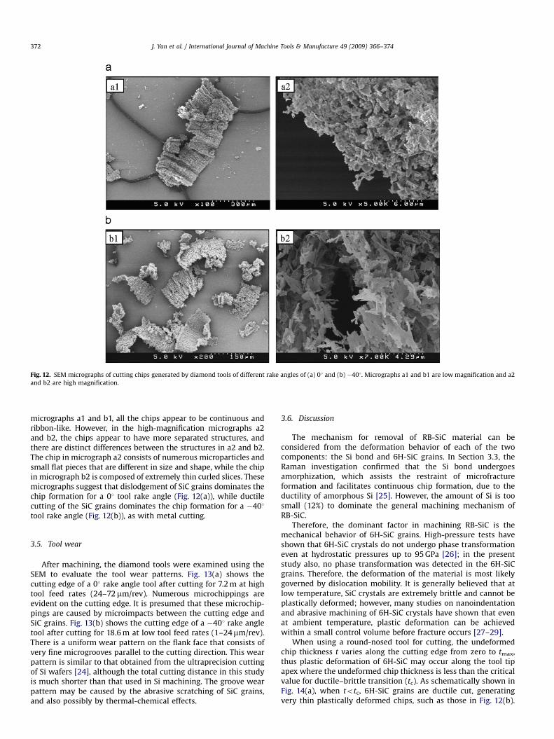
The cutting chips were collected and observed using SEM.Fig. 12(a) and (b) shows two pairs of different magnification SEMmicrographs of the chips produced by diamond tools of differentrake angles 01 and �401, respectively. In the low-magnification
ARTICLE IN PRESS
Fig. 12. SEM micrographs of cutting chips generated by diamond tools of different rake angles of (a) 01 and (b) �401. Micrographs a1 and b1 are low magnification and a2
and b2 are high magnification.
J. Yan et al. / International Journal of Machine Tools & Manufacture 49 (2009) 366–374372
micrographs a1 and b1, all the chips appear to be continuous andribbon-like. However, in the high-magnification micrographs a2and b2, the chips appear to have more separated structures, andthere are distinct differences between the structures in a2 and b2.The chip in micrograph a2 consists of numerous microparticles andsmall flat pieces that are different in size and shape, while the chipin micrograph b2 is composed of extremely thin curled slices. Thesemicrographs suggest that dislodgement of SiC grains dominates thechip formation for a 01 tool rake angle (Fig. 12(a)), while ductilecutting of the SiC grains dominates the chip formation for a �401tool rake angle (Fig. 12(b)), as with metal cutting.
3.5. Tool wear
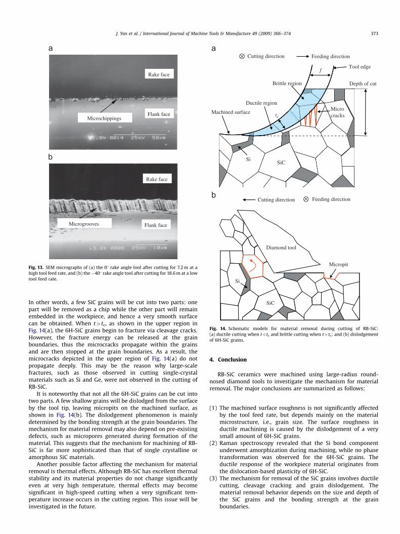
After machining, the diamond tools were examined using theSEM to evaluate the tool wear patterns. Fig. 13(a) shows thecutting edge of a 01 rake angle tool after cutting for 7.2 m at hightool feed rates (24–72mm/rev). Numerous microchippings areevident on the cutting edge. It is presumed that these microchip-pings are caused by microimpacts between the cutting edge andSiC grains. Fig. 13(b) shows the cutting edge of a �401 rake angletool after cutting for 18.6 m at low tool feed rates (1–24mm/rev).There is a uniform wear pattern on the flank face that consists ofvery fine microgrooves parallel to the cutting direction. This wearpattern is similar to that obtained from the ultraprecision cuttingof Si wafers [24], although the total cutting distance in this studyis much shorter than that used in Si machining. The groove wearpattern may be caused by the abrasive scratching of SiC grains,and also possibly by thermal-chemical effects.
3.6. Discussion
The mechanism for removal of RB-SiC material can beconsidered from the deformation behavior of each of the twocomponents: the Si bond and 6H-SiC grains. In Section 3.3, theRaman investigation confirmed that the Si bond undergoesamorphization, which assists the restraint of microfractureformation and facilitates continuous chip formation, due to theductility of amorphous Si [25]. However, the amount of Si is toosmall (12%) to dominate the general machining mechanism ofRB-SiC.
Therefore, the dominant factor in machining RB-SiC is themechanical behavior of 6H-SiC grains. High-pressure tests haveshown that 6H-SiC crystals do not undergo phase transformationeven at hydrostatic pressures up to 95 GPa [26]; in the presentstudy also, no phase transformation was detected in the 6H-SiCgrains. Therefore, the deformation of the material is most likelygoverned by dislocation mobility. It is generally believed that atlow temperature, SiC crystals are extremely brittle and cannot beplastically deformed; however, many studies on nanoindentationand abrasive machining of 6H-SiC crystals have shown that evenat ambient temperature, plastic deformation can be achievedwithin a small control volume before fracture occurs [27–29].
When using a round-nosed tool for cutting, the undeformedchip thickness t varies along the cutting edge from zero to tmax,thus plastic deformation of 6H-SiC may occur along the tool tipapex where the undeformed chip thickness is less than the criticalvalue for ductile–brittle transition (tc). As schematically shown inFig. 14(a), when totc, 6H-SiC grains are ductile cut, generatingvery thin plastically deformed chips, such as those in Fig. 12(b).
ARTICLE IN PRESS
Rake face
Flank face
Rake face
Flank face Microgrooves
Microchippings
Fig. 13. SEM micrographs of (a) the 01 rake angle tool after cutting for 7.2 m at a
high tool feed rate, and (b) the �401 rake angle tool after cutting for 18.6 m at a low
tool feed rate.
Tool edge
Feeding direction
Depth of cut
tcMachined surface
Ductile region
Brittle region
Cutting direction
f
SiSiC
Microcracks
Cutting direction Feeding direction
Diamond tool
Micropit
Si
SiC
Fig. 14. Schematic models for material removal during cutting of RB-SiC:
(a) ductile cutting when totc and brittle cutting when t4tc; and (b) dislodgement
of 6H-SiC grains.
J. Yan et al. / International Journal of Machine Tools & Manufacture 49 (2009) 366–374 373
In other words, a few SiC grains will be cut into two parts: onepart will be removed as a chip while the other part will remainembedded in the workpiece, and hence a very smooth surfacecan be obtained. When t4tc, as shown in the upper region inFig. 14(a), the 6H-SiC grains begin to fracture via cleavage cracks.However, the fracture energy can be released at the grainboundaries, thus the microcracks propagate within the grainsand are then stopped at the grain boundaries. As a result, themicrocracks depicted in the upper region of Fig. 14(a) do notpropagate deeply. This may be the reason why large-scalefractures, such as those observed in cutting single-crystalmaterials such as Si and Ge, were not observed in the cutting ofRB-SiC.
It is noteworthy that not all the 6H-SiC grains can be cut intotwo parts. A few shallow grains will be dislodged from the surfaceby the tool tip, leaving micropits on the machined surface, asshown in Fig. 14(b). The dislodgement phenomenon is mainlydetermined by the bonding strength at the grain boundaries. Themechanism for material removal may also depend on pre-existingdefects, such as micropores generated during formation of thematerial. This suggests that the mechanism for machining of RB-SiC is far more sophisticated than that of single crystalline oramorphous SiC materials.
Another possible factor affecting the mechanism for materialremoval is thermal effects. Although RB-SiC has excellent thermalstability and its material properties do not change significantlyeven at very high temperature, thermal effects may becomesignificant in high-speed cutting when a very significant tem-perature increase occurs in the cutting region. This issue will beinvestigated in the future.
4. Conclusion
RB-SiC ceramics were machined using large-radius round-nosed diamond tools to investigate the mechanism for materialremoval. The major conclusions are summarized as follows:
(1)
The machined surface roughness is not significantly affectedby the tool feed rate, but depends mainly on the materialmicrostructure, i.e., grain size. The surface roughness inductile machining is caused by the dislodgement of a verysmall amount of 6H-SiC grains.(2)
Raman spectroscopy revealed that the Si bond componentunderwent amorphization during machining, while no phasetransformation was observed for the 6H-SiC grains. Theductile response of the workpiece material originates fromthe dislocation-based plasticity of 6H-SiC.(3)
The mechanism for removal of the SiC grains involves ductilecutting, cleavage cracking and grain dislodgement. Thematerial removal behavior depends on the size and depth ofthe SiC grains and the bonding strength at the grainboundaries.
ARTICLE IN PRESS
J. Yan et al. / International Journal of Machine Tools & Manufacture 49 (2009) 366–374374
(4)
Large-scale fractures do not occur during cutting of RB-SiC,due to the ductile response of the Si bond and fracture energyreleasing effects at the grain boundaries. This feature enablesthe precision machining of RB-SiC at a very high materialremoval rate.(5)
Tool wear can be classified into two types: One is themicrochipping that occurs on zero rake angle tools underhigh feed conditions; the other is microgrooved flank wearthat occurs for highly negative rake angle tools under feedconditions.Acknowledgements
The authors would like to express their appreciation to JapanFine Ceramics Co., Ltd. for providing the RB-SiC samples andtechnical data. This work has been partially supported by theJapan Society for the Promotion of Science, Grant-in-Aid forScience Research (B), project number 19360055.
References
[1] C. Hall, M. Tricard, H. Murakoshi, Y. Yamamoto, K. Kuriyama, H. Yoko, Newmold manufacturing techniques, Proceedings of the SPIE 5868 (2005)58680V.
[2] S. Suyama, T. Kameda, Y. Itoh, Development of high-strength reaction-sinteredsilicon carbide, Diamond and Related Materials 12 (2003) 1201–1204.
[3] S. Suyama, Y. Itoh, K. Tsuno, K. Ohno, F650 mm optical space mirror substrateof high-strength reaction-sintered silicon carbide, Proceedings of SPIE 5868(2005) 58680E.
[4] H. Toshiya, I. Ichiro, S. Junichi, Grinding of silicon carbide with diamondwheel, Transactions of the Japan Society of Mechanical Engineers C 51 (1985)1864–1870.
[5] Y. Dai, H. Ohmori, W. Lin, H. Eto, N. Ebizuka, K. Tsuno, ELID grinding propertiesof high-strength reaction-sintered SiC, Key Engineering Materials 291–292(2005) 121–126.
[6] H.Y. Tam, H.B. Cheng, Y.W. Wang, Removal rate and surface roughness in thelapping and polishing of RB-SiC optical components, Journal of MaterialsProcessing Technology 192–193 (2007) 276–280.
[7] H. Cheng, Z. Feng, S. Lei, Y. Wang, Magnetorheological finishing of SiC asphericmirrors, Materials and Manufacturing Processes 20 (6) (2005) 917–931.
[8] H. Kitahara, Y. Noda, F. Yoshida, H. Nakashima, N. Shinohara, H. Abe,Mechanical behavior of single crystalline and polycrystalline silicon carbidesevaluated by Vickers indentation, Journal of the Ceramic Society of Japan 109(2001) 602–606.
[9] T. Nakasuji, S. Kodera, S. Hara, H. Matsunaga, N. Ikawa, S. Shimada, Diamondturning of brittle materials for optical components, Annals of the CIRP 39(1990) 89–92.
[10] P.N. Blake, R.O. Scattergood, Diamond turning of brittle materials for opticalcomponents, Journal of the American Ceramic Society 73 (1990) 949–957.
[11] J. Yan, K. Syoji, T. Kuriyagawa, H. Suzuki, Ductile regime turning at large toolfeed, Journal of Materials Processing Technology 121 (2002) 363–372.
[12] J. Yan, K. Maekawa, J. Tamaki, T. Kuriyagawa, Micro grooving on single-crystalgermanium for infrared Fresnel lenses, Journal of Micromechanics andMicroengineering 15 (2005) 1925–1931.
[13] T. Ohta, J. Yan, S. Yajima, Y. Takahashi, N. Horikawa, T. Kuriyagawa, High-efficiency machining of single-crystal germanium using large-radius diamondtools, International Journal of Surface Science and Engineering 1 (2007)374–392.
[14] J. Patten, W. Gao, K. Yasuto, Ductile regime nanomachining of single-crystalsilicon carbide, ASME Journal of Manufacturing Science and Engineering 127(2005) 522–532.
[15] B. Bhattacharya, J. Patten, J. Jacob, Single point diamond turning of CVDcoated silicon carbide, in: Proceedings of 2006 ASME InternationalConference on Manufacturing Science and Engineering, October 8–11,Ypsilanti, Michigan, USA, 2006, pp. 1–6.
[16] J.P. Davim, Jose Silva, A.M. Baptista, Experimental cutting model of metalmatrix composites (MMCs), Journal of Materials Processing Technology 183(2007) 358–362.
[17] Y. Wang, L.J. Yang, N. Wang, An investigation of laser-assisted machining ofAl2O3 particle reinforced aluminum matrix composite, Journal of MaterialsProcessing Technology 129 (2002) 268–272.
[18] T. Ozben, E. Kilickap, O. Cakır, Investigation of mechanical and machinabilityproperties of SiC particle reinforced Al-MMC, Journal of Materials ProcessingTechnology 198 (2008) 220–225.
[19] Y.F. Ge, J.H. Xu, H. Yang, S.B. Luo, Y.C. Fu, Workpiece surface quality whenultra-precision turning of SiCp/Al composites, Journal of Materials ProcessingTechnology 203 (2008) 166–175.
[20] J. Yan, M. Yoshino, T. Kuriyagawa, T. Shirakashi, K. Syoji, R. Komanduri, On theductile machining of silicon for micro electro-mechanical systems (MEMS),opto-electronic and optical applications, Materials Science and EngineeringA 297 (2001) 230–234.
[21] S. Nakashima, H. Harima, Raman investigation of SiC polytypes, PhysicaStatus Solidi A 162 (1997) 39–64.
[22] J. Yan, Laser micro-Raman spectroscopy of single-point diamond machinedsilicon substrates, Journal of Applied Physics 95 (4) (2004) 2094–2101.
[23] J. Yan, T. Asami, T. Kuriyagawa, Nondestructive measurement of themachining-induced amorphous layers in single-crystal silicon by lasermicro-Raman spectroscopy, Precision Engineering 32 (2008) 186–195.
[24] J. Yan, K. Syoji, J. Tamaki, Some observations on the wear of diamond toolsin ultra-precision cutting of single-crystal silicon, Wear 255 (2003)1380–1387.
[25] J. Yan, H. Takahashi, J. Tamaki, X. Gai, T. Kuriyagawa, Transmission electronmicroscopic observation of nanoindentations made on ductile-machinedsilicon wafers, Applied Physics Letters 87 (2005) 211901.
[26] M. Yoshida, A. Onodera, M. Ueno, K. Takemura, O. Shimomura, Pressure-induced phase transition in SiC, Physical Review B 48 (1993) 10587–10590.
[27] L. Yin, E.Y.J. Vancoille, K. Ramesh, H. Huang, Surface characterization of 6H-SiC (0 0 0 1) substrates in indentation and abrasive machining, InternationalJournal of Machine Tools and Manufacture 44 (2004) 607–615.
[28] S. Shim, J. Jang, G.M. Pharr, Extraction of flow properties of single-crystalsilicon carbide by nanoindentation and finite-element simulation, ActaMaterialia 56 (2008) 3824–3832.
[29] J.R. Grim, M. Benamara, M. Skowronski, W.J. Everson, V.D. Heydemann,Transmission electron microscopy analysis of mechanical polishing-relateddamage in silicon carbide wafers, Semiconductor Science and Technology 21(2006) 1709–1713.