best practices for half-bridge gate drivers for hev/ev
TRANSCRIPT
Best practices for half-bridge drivers for HEV/EV
High Voltage Seminar 2021
Jackie Hui
1
Acknowledgement: Richard Herring, Applications Engineer

Agenda
• Mid-voltage half-bridge design considerations
– Bootstrap supply design consideration
– Switch node noise handling
– Ground noise handling
– Traditional half-bridge driver architecture vs. new UCC2792x
• Using half-bridge driver for high side switch control
– Introduce the design circuit
– Application examples
2
• Relevant applications
Part numbers mentioned:
• UCC27282(-Q1)
• UCC27284(-Q1)
• UCC27289
• UCC27212(-Q1)
• UCC27928A(-Q1)
• UCC27925B-Q1

Bootstrap supply design consideration
3
LO on to charge Cboot
Discharge Cboot to supply high
side HO on-pulse drive duration
Basic bootstrap circuit operation

Bootstrap supply design consideration
Bootstrap cap value Potential issue
Too small • Higher output ripple voltage
• Inadequate charge to drive high side FET
• High dv/dt at initial bootstrap charge up
Too large • High bootstrap Ipeak
• Take longer time to charge, require longer
low side on time
Rule of thumb: Cboot ≥ 10x of FET gate capacitance
More detail calculation:
Also to consider
– Boot capacitor
• low ESR, ESL, X7R cap for better temperature coefficients
– Very high fsw such as >1MHz
• Can add a low value, high frequency bypass cap in parallel of Cboot
– Low fsw such as ~10kHz in motor drive application
• take account for Rgs loading or any other leakage path from HS to VSS
– VDD bypass capacitor
• ≥ 10 x Cboot
• Reduce VDD ripple and avoid driver UVLO4
Cboot ≥ Qtotal/ΔVHB
• Qtotal = Qg + IHBS x (DMax/fsw) + (IHB/fsw)• ΔVHB = VDD – VDH – VHBL
Bootstrap cap selection

Bootstrap supply design consideration
5
Bootstrap diode consideration:
• Use fast reverse recovery or Schottky diode
– Reduce risk of current supplies back to driver supply from bootstrap capacitor
• Able to take Ipeak during initial bootstrap cap startup
• Voltage rating shall take into account Vbus transient
During boot diode reverse recovery
• Undershoot can cause driver shutdown
• Can also increase switch node ringing
High dv/dt cause by high Ipeak
• Can cause undesired pulse on outputs
• Or may damage to driver
Bootstrap diode selection

Bootstrap supply design consideration
6
Optimum startup sequence Control inputs switch before UVLO delay expire
Missing pulse
Partial pulse
• Controller should allow driver bias UVLO delay to expire before driving starting pulse
• Bootstrap cap value shall take into account the high side bias UVLO delay to ensure adequate capacitance is
considered in the design
Bias supply startup sequence

Switch node noise handling
Possible issues:
➢ Driver malfunction (faulty input pulse translation with increased ground noise)
➢ Bootstrap diode overcurrent
➢ High side bias (HB-HS) overvoltage
7
Cause of negative spike
1. While high side turning off, low side turning on
2. Current flow in the inductance, low side current rising
3. Power device/pcb layout parasitic inductance causes the –ve voltage
on the switch node
di/dt
Lss * di/dt
What’s causing the negative spike?

Switch node noise handling
• Reduce parasitic inductance
– Most parasitic inductance is from the layout
8
Po
wer F
ET
s
Bulk caps
Bulk cap usually is not close to the power
FETs
➢ Parasitic inductance from low side FET source
to capacitor
Add a ceramic cap across the power MOSFET
➢ Reduce the parasitic inductance from low side
FET source to capacitors
How to reduce negative spike?

Switch node and drive output noise handling
• Clamp the negative spike
– Add a zener diode between HB-HS
– Prevent HB-HS overvoltage
• Limit current into HS (With internal Dboot)
– Place small resistor (e.g. 2Ω) at the switch node
– Reduce switch node slew rate and noise
9
• Reduce current in
discharge paths
How to reduce negative spike?

Ground noise handling
10
1
2
1. Ideal case: current from low side FET source to return
to the system ground (to the bulk capacitors)
2. The ground noise can affect the driver input signals
through the low side FET source to driver ground
connection
May result with undesired input signal translates
to output pulse
Drive input noise

Ground noise handling
11
1. Add small RC filter on the
input signal pins
2. RC filter should be placed on
a clean ground close to the
driver input pins
1. Increase impedance connection on between
the controller and power train grounds
2. Narrow layout trace width connecting the
controller and power grounds
Mitigate Drive input noise: schematic layout

Ground noise handling
12
• Minimum input pulse rejection
– UCC27282/284: 20ns
– UCC27925/928: 20ns
• Input interlock and deadtime− UCC27282: Interlock
− UCC27925: resistor programmable 60x deadtime
− UCC27928: resistor programmable 10x deadtime
• Negative voltage transients support− UCC27282/284:
• Switch node HS @-14V for <100ns
• Input pins HI, LI, EN @-5V
− UCC27925/928:• Switch node @ -200V
• Split input and power grounds @+/-200V
Deadtime function
Minimum input pulse rejection (e.g. on pulse)
Mitigate Drive input noise: driver features

Half-bridge driver architecture vs. new UCC2792x • Traditional HB driver architecture
13
Vbus
SGND
VBias
GND
Q2
Q1
SW
CBoot
DBootRBoot
HI
PWM1
PWM2LI
GND
LO
VDD
VDDVDD
Level Shift
No
ise
Can
cell
er
HO
HB
HS
GND
GND
• LO: Low side output
• drive the ground reference MOSFET• Gate voltage = VDD
• HO: High side output
• Floating driver with HS as reference• Gate voltage = VDD – boot diode Vf w.r.t. HS
• UCC2792x architecture
• Split grounds with +/-200V
• Level shifter on both high and low side output➢ Excellent ground noise immunity
• Low side power by VDD2
• High side powered by VDD1 (can be bootstrap from VDD2)➢ Excellent switch node noise tolerance
• UCC27925A-Q1: 8V UVLO, 60x Deadtime
• UCC27928A-Q1: 4V UVLO, 10x Deadtime

UCC2792x: bootstrap supply design
14
VDD UVLO
level
Output switch in <5us
dv/dt in ~1.34V/ns
VDD UVLO delay: spec typ 2us
• Fast start up allows faster
switching
VDD dv/dt delay: spec max
0.5V/ns
• Higher dv/dt tolerance
improve driver robustness
Test setup
Short VDD UVLO delay + high startup dv/dt tolerance
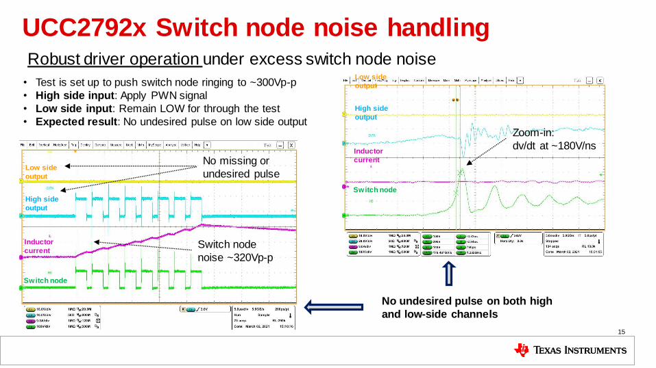
UCC2792x Switch node noise handling
15
• Test is set up to push switch node ringing to ~300Vp-p
• High side input: Apply PWN signal
• Low side input: Remain LOW for through the test
• Expected result: No undesired pulse on low side output
No undesired pulse on both high
and low-side channels
High side
output
Switch node
Low side
output
Inductor
currentSwitch node
noise ~320Vp-p
No missing or
undesired pulse
High side
output
Switch node
Low side
output
Inductor
current
Zoom-in:
dv/dt at ~180V/ns
Robust driver operation under excess switch node noise

UCC2792x ground noise handling
16
Application with single ground, suffering
• Severe ground bounds
• Ground shifted because of a use of current sense resistor
Example: Half-bridge in 48-V motor drive design
VDD2
OUT2
VSS2
VDD1
OUT1
VSS1
VBIAS
VBIAS
VBUS
SW
DT
EN
GND
IN2
IN1
VCCI
GND
RDT
GND
MCU supply
PWM1
PWM2
DBOOT
CBOOT
Q1
Q2
UCC27925B-Q1
+/-200 VWith <0.01uA max leakage
Split grounds and application examples

UCC2792x ground noise handling
Example: Unidirectional 48V-12V DC/DC
17
48V12V
UCC27928A-Q1
48V 12V
UCC27928A-Q1
as half-bridge x2
UCC27928A-Q1
as dual low side
uC
uC
Example: bi-directional 48V-12V DC/DC
Configure as dual low side
• Use as SR driver for best
ground bounce immunity
12-V side
controller
48-V side
Power MOSFET
Allow clean 48-V & 12-V
ground layout design
Split grounds and application examples

Using half-bridge driver as high-side switch control
• What is high side switch?
– Switches placed between voltage source and load
• Why using high side switch?
– No floating voltages at load
– System is pulled to ground
• Mechanical relay constraints
– Good
• can control high voltage system from a low power single
– Bad
• subject to wear out due to friction/oxidation
• shorter cycling lifetime comparing solid state relay
• slower reaction time
➢ Use high side driver + MOSFET
18
Example: DC circuit breaker in 48-V-12-V DC/DC
Example: Battery disconnect in 48-V/12-V battery system
Why mechanical relay is being replaced by
solid state solution

Using half-bridge driver as high-side switch control
• High power, high current application challenge
– Integrated MOSFET/driver cannot support high current
– System has multiple MOSFEs in parallel
• Higher gate charge (Qg)
• Still requires fast switching
– 12V, 48V system require different driver voltage rating
➢ Driver requirements
• Support 100% duty cycle
• Strong drive strength
• Different driver voltage rating options
• Cost effective solution
19
Self-oscillate circuit
Charge pump
Half-bridge driver + external charge pump
UCC27284-Q1
Gate driver and MOSFET as solid state disconnect switch
Using half-bridge driver as high-side switch control
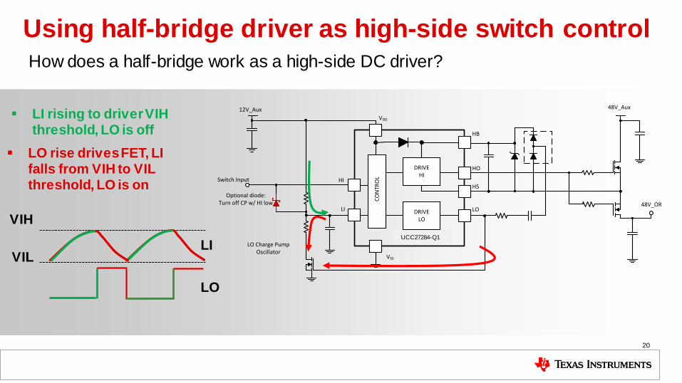
20
12V_Aux
Switch Input
48V_Aux
48V_OR
CO
NTR
OL
DRIVELO
DRIVEHI
VDD
UCC27212
VSS
LI
HB
HO
HS
LO
HI
LO Charge PumpOscillator
Optional diode:Turn off CP w/ HI low
▪ LI rising to driver VIH threshold, LO is off
▪ LO rise drives FET, LI falls from VIH to VIL threshold, LO is on
VIH
VILLI
LO
UCC27284-Q1
How does a half-bridge work as a high-side DC driver?
Using half-bridge driver as high-side switch control
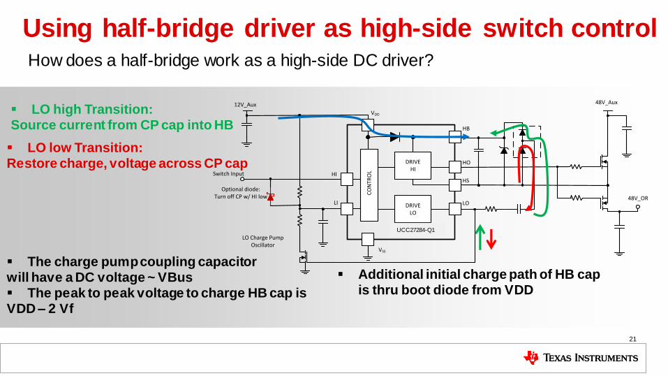
21
12V_Aux
Switch Input
48V_Aux
48V_OR
CO
NTR
OL
DRIVELO
DRIVEHI
VDD
UCC27212
VSS
LI
HB
HO
HS
LO
HI
LO Charge PumpOscillator
Optional diode:Turn off CP w/ HI low
▪ LO high Transition:Source current from CP cap into HB
▪ LO low Transition:Restore charge, voltage across CP cap
▪ The charge pump coupling capacitorwill have a DC voltage ~ VBus▪ The peak to peak voltage to charge HB cap is VDD – 2 Vf
▪ Additional initial charge path of HB cap is thru boot diode from VDD
UCC27284-Q1
How does a half-bridge work as a high-side DC driver?

Using half-bridge driver as high-side switch control
• Half-bridge driver selection
– For charge pump operation, both HO & LO need to
be on
• Select driver without interlock
– LI input has oscillator ramp waveform
• Select driver with sufficient VIH and VIL
hysteresis
• Example drivers for the application
• Alternative circuit for driver with interlock function
22
Device Input
Hyst
VHS Max
Recom
Driver
Current
VDD UVLO
Max
UCC27284(-Q1) 1.0 V 100 V 2.5/3.5 A 5.4
UCC27289 1.0 V 100 V 2.5/3.5 A 8• Bypass interlock with TLV1805 (high voltage
comparator) as charge pump oscillator • UCC27712-Q1: 600V, 2A with interlock
Driver selection

©2021 Texas Instruments Incorporated. All rights reserved.
SLYP766

IMPORTANT NOTICE AND DISCLAIMERTI PROVIDES TECHNICAL AND RELIABILITY DATA (INCLUDING DATASHEETS), DESIGN RESOURCES (INCLUDING REFERENCEDESIGNS), APPLICATION OR OTHER DESIGN ADVICE, WEB TOOLS, SAFETY INFORMATION, AND OTHER RESOURCES “AS IS”AND WITH ALL FAULTS, AND DISCLAIMS ALL WARRANTIES, EXPRESS AND IMPLIED, INCLUDING WITHOUT LIMITATION ANYIMPLIED WARRANTIES OF MERCHANTABILITY, FITNESS FOR A PARTICULAR PURPOSE OR NON-INFRINGEMENT OF THIRDPARTY INTELLECTUAL PROPERTY RIGHTS.These resources are intended for skilled developers designing with TI products. You are solely responsible for (1) selecting the appropriateTI products for your application, (2) designing, validating and testing your application, and (3) ensuring your application meets applicablestandards, and any other safety, security, or other requirements. These resources are subject to change without notice. TI grants youpermission to use these resources only for development of an application that uses the TI products described in the resource. Otherreproduction and display of these resources is prohibited. No license is granted to any other TI intellectual property right or to any third partyintellectual property right. TI disclaims responsibility for, and you will fully indemnify TI and its representatives against, any claims, damages,costs, losses, and liabilities arising out of your use of these resources.TI’s products are provided subject to TI’s Terms of Sale (https:www.ti.com/legal/termsofsale.html) or other applicable terms available eitheron ti.com or provided in conjunction with such TI products. TI’s provision of these resources does not expand or otherwise alter TI’sapplicable warranties or warranty disclaimers for TI products.IMPORTANT NOTICE
Mailing Address: Texas Instruments, Post Office Box 655303, Dallas, Texas 75265Copyright © 2021, Texas Instruments Incorporated