data sheet - d3uzseaevmutz1.cloudfront.net · ds1081f4 2 cs43l36 general description the cs43l36 is...
TRANSCRIPT

AS
AS
AS
TIP
*
*
ly
CS43L36
Low-Power, High-Performance Audio DAC with Class H Headphone Drivers
System Features• Stereo headphone (HP) output with 114-dB dynamic range
— Class H HP amplifier with four-level automatic or manual supply adjust
— –98-dB THD+N into 30 with 10-mW output power— 2 x 35 mW output power into 30 with 0.018%
THD+N
• Load detection— Headphone load detection of 15 or 30 — Line-level load (3 k) with capacitance detection
• Headphone insertion/removal detection with WAKE
• Audio serial port (ASP)— I2S (two channels) or TDM (up to four channels) — Slave or Hybrid-Master Mode (bit-clock slave and
LRCK/FSYNC derived from bit clock)— Supports up to 32-bit audio— Sample rate support for 8 to 192 kHz— I2C control with interrupt output
• Integrated fractional-N PLL — Increases system-clock flexibility for audio processing— Reference clock sourced from I2S/TDM bit clock
• Bypassable SRCs for maximum flexibility
• Attenuation, mute, and volume controls for each output
• Integrated power management— Digital core operates from either an external 1.2-V
supply or LDO from a 1.8-V supply.— Step-down charge pump improves HP efficiency— Independent peripheral power-down controls— Standby operation from VP with all other supplies
powered off — VP monitor to detect and report brownout conditions— Low-impedance switching suppresses ground-noise
Applications• Ultrabooks, tablets, and smartphones
• Digital headsets
PLLClock Gen MCLK
Interpolator and
Volume ControlP_SDIN
P_SCLK
P_LRCK/FSYNC
SCLSDA
Pseudodifferential Input
Headphone Detect
HS3
_SENSE
INT
Digital AudioInput
I2C Slave
SRC
SRC
Headset Impedance Detect and Switches
WAKE AD0 AD1
HS3_REF
VL VD_FILT
LDOwith
Bypass
DIGLDO_PDN
+VCP_FILT
–VCP_FILT
VA
Inverting
Step-DownLDO
VP
Analog Core POR
VCP
VP_CP
DigitalCore
CS43L36
Interpolator and
Volume Control
Multibit Modulator
DACMultibit Modulator HPOUTB
–VCP_FILT
HPOUTA
+VCP_FILT
–VCP_FILT
+VCP_FILT
HPSENSA
–
+
–
+
HPSENSB
* WLCSP package on
DAC
Copyright Cirrus Logic, Inc. 2014–2018(All Rights Reserved)
http://www.cirrus.com
DS1081F4DEC ’18

CS43L36
General DescriptionThe CS43L36 is a low-power, high dynamic-range, stereo audio DAC with integrated I2S/I2C/TDM interfaces designed for portable applications. The CS43L36 features support for up to 32-bit audio inputs and includes bypassable SRCs.
The bypassable fractional-N PLL sourced from the ASP SCLK allows for maximum flexibility in any system.
There is independent attenuation on each input along with volume adjustment and mute control.
The CS43L36 is available in 49-ball WLCSP package and a 40-pin QFN package, both supporting an extended commercial operational temperature range of –40°C to +85°C.
DS1081F4 2

CS43L36
Table of Contents1 Pin Assignments and Descriptions . . . . . . . . . . . . . . . . . . . . . . 4
1.1 WLCSP Pin Out (Through-Package View) . . . . . . . . . . . . . . 41.2 QFN Pin Out (Through-Package View) . . . . . . . . . . . . . . . . . 51.3 Pin Descriptions . . . . . . . . . . . . . . . . . . . . . . . . . . . . . . . . . . 51.4 Electrostatic Discharge (ESD) Protection Circuitry . . . . . . . . 7
2 Typical Connections . . . . . . . . . . . . . . . . . . . . . . . . . . . . . . . . . 102.1 Electromagnetic Compatibility (EMC) Circuitry . . . . . . . . . . 11
3 Characteristics and Specifications . . . . . . . . . . . . . . . . . . . . . 12Table 3-1. Parameter Definitions . . . . . . . . . . . . . . . . . . . . . . . . . . . . . .12Table 3-2. Recommended Operating Conditions . . . . . . . . . . . . . . . . .12Table 3-3. Absolute Maximum Ratings . . . . . . . . . . . . . . . . . . . . . . . . .12Table 3-4. Combined DAC Digital, On-Chip Analog, and HPOUTx
Filter Characteristics . . . . . . . . . . . . . . . . . . . . . . . . . . . . . . . . . . . . . .13Table 3-5. DAC High-Pass Filter (HPF) Characteristics . . . . . . . . . . . .13Table 3-6. SDIN to HPOUTx with SRC-Enabled Datapath
Characteristics . . . . . . . . . . . . . . . . . . . . . . . . . . . . . . . . . . . . . . . . . . .13Table 3-7. Serial Data In-to-HPOUTx Characteristics . . . . . . . . . . . . . .14Table 3-8. DC Characteristics . . . . . . . . . . . . . . . . . . . . . . . . . . . . . . . .15Table 3-9. Power-Supply Rejection Ratio (PSRR) Characteristics . . . .15Table 3-10. Power Consumption . . . . . . . . . . . . . . . . . . . . . . . . . . . . . .16Table 3-11. Register Field Settings . . . . . . . . . . . . . . . . . . . . . . . . . . . .16Table 3-12. Digital Audio Interface Timing Characteristics . . . . . . . . . .17Table 3-13. I2C Slave Port Characteristics . . . . . . . . . . . . . . . . . . . . . .17Table 3-14. Digital Interface Specifications and Characteristics . . . . . .19
4 Functional Description . . . . . . . . . . . . . . . . . . . . . . . . . . . . . . . 204.1 Digital Volume Control . . . . . . . . . . . . . . . . . . . . . . . . . . . . . 214.2 Analog Output . . . . . . . . . . . . . . . . . . . . . . . . . . . . . . . . . . . 224.3 Class H Amplifier . . . . . . . . . . . . . . . . . . . . . . . . . . . . . . . . . 234.4 Clocking Architecture . . . . . . . . . . . . . . . . . . . . . . . . . . . . . 284.5 Audio Serial Port (ASP) . . . . . . . . . . . . . . . . . . . . . . . . . . . . 344.6 Sample-Rate Converters (SRCs) . . . . . . . . . . . . . . . . . . . . 404.7 Headset Interface . . . . . . . . . . . . . . . . . . . . . . . . . . . . . . . . 414.8 Plug Presence Detect . . . . . . . . . . . . . . . . . . . . . . . . . . . . . 414.9 Power-Supply Considerations . . . . . . . . . . . . . . . . . . . . . . . 434.10 Control-Port Operation . . . . . . . . . . . . . . . . . . . . . . . . . . . 454.11 Reset . . . . . . . . . . . . . . . . . . . . . . . . . . . . . . . . . . . . . . . . . 474.12 Interrupts . . . . . . . . . . . . . . . . . . . . . . . . . . . . . . . . . . . . . . 474.13 FILT+ Operation . . . . . . . . . . . . . . . . . . . . . . . . . . . . . . . . 48
5 System Applications . . . . . . . . . . . . . . . . . . . . . . . . . . . . . . . . . 495.1 Power-Up Sequence . . . . . . . . . . . . . . . . . . . . . . . . . . . . . . 495.2 Power-Down Sequence . . . . . . . . . . . . . . . . . . . . . . . . . . . . 515.3 Page 0x30 Read Sequence . . . . . . . . . . . . . . . . . . . . . . . . 525.4 PLL Clocking . . . . . . . . . . . . . . . . . . . . . . . . . . . . . . . . . . . . 525.5 VD_FILT/VL ESD Diode . . . . . . . . . . . . . . . . . . . . . . . . . . . 52
6 Register Quick Reference . . . . . . . . . . . . . . . . . . . . . . . . . . . . 536.1 Global Registers . . . . . . . . . . . . . . . . . . . . . . . . . . . . . . . . . 536.2 Power-Down and Headset-Detect Registers . . . . . . . . . . . . 546.3 Clocking Registers . . . . . . . . . . . . . . . . . . . . . . . . . . . . . . . 556.4 Interrupt Registers . . . . . . . . . . . . . . . . . . . . . . . . . . . . . . . . 556.5 Fractional-N PLL Registers . . . . . . . . . . . . . . . . . . . . . . . . . 566.6 HP Load Detect Registers . . . . . . . . . . . . . . . . . . . . . . . . . . 576.7 Headset Interface Registers . . . . . . . . . . . . . . . . . . . . . . . . 576.8 DAC Registers . . . . . . . . . . . . . . . . . . . . . . . . . . . . . . . . . . . 586.9 HP Control Registers . . . . . . . . . . . . . . . . . . . . . . . . . . . . . . 586.10 Class H Registers . . . . . . . . . . . . . . . . . . . . . . . . . . . . . . . 586.11 Mixer Volume Registers . . . . . . . . . . . . . . . . . . . . . . . . . . 586.12 AudioPort Interface Registers . . . . . . . . . . . . . . . . . . . . . . 596.13 SRC Registers . . . . . . . . . . . . . . . . . . . . . . . . . . . . . . . . . . 596.14 Serial Port Receive Registers . . . . . . . . . . . . . . . . . . . . . . 596.15 ID Registers . . . . . . . . . . . . . . . . . . . . . . . . . . . . . . . . . . . . 60
7 Register Descriptions . . . . . . . . . . . . . . . . . . . . . . . . . . . . . . . . 607.1 Global Registers . . . . . . . . . . . . . . . . . . . . . . . . . . . . . . . . . 607.2 Power Down and Headset Detects . . . . . . . . . . . . . . . . . . . 637.3 Clocking Registers . . . . . . . . . . . . . . . . . . . . . . . . . . . . . . . 657.4 Interrupt Registers . . . . . . . . . . . . . . . . . . . . . . . . . . . . . . . . 687.5 Fractional-N PLL Registers . . . . . . . . . . . . . . . . . . . . . . . . . 727.6 HP Load-Detect Registers . . . . . . . . . . . . . . . . . . . . . . . . . . 747.7 Headset Interface Registers . . . . . . . . . . . . . . . . . . . . . . . . 747.8 DAC Control Registers . . . . . . . . . . . . . . . . . . . . . . . . . . . . 767.9 HP Control Register . . . . . . . . . . . . . . . . . . . . . . . . . . . . . . 777.10 Class H Register . . . . . . . . . . . . . . . . . . . . . . . . . . . . . . . . 777.11 Volume Control . . . . . . . . . . . . . . . . . . . . . . . . . . . . . . . . . 777.12 AudioPort Interface Registers . . . . . . . . . . . . . . . . . . . . . . 787.13 SRC Registers . . . . . . . . . . . . . . . . . . . . . . . . . . . . . . . . . . 79
7.14 Serial Port Receive Registers . . . . . . . . . . . . . . . . . . . . . . 797.15 ID Registers . . . . . . . . . . . . . . . . . . . . . . . . . . . . . . . . . . . . 81
8 PCB Layout Considerations . . . . . . . . . . . . . . . . . . . . . . . . . . . 828.1 Power Supply . . . . . . . . . . . . . . . . . . . . . . . . . . . . . . . . . . . . 828.2 Grounding . . . . . . . . . . . . . . . . . . . . . . . . . . . . . . . . . . . . . . . 828.3 QFN Thermal Pad . . . . . . . . . . . . . . . . . . . . . . . . . . . . . . . . 82
9 Plots . . . . . . . . . . . . . . . . . . . . . . . . . . . . . . . . . . . . . . . . . . . . . . 839.1 Digital Filter Response . . . . . . . . . . . . . . . . . . . . . . . . . . . . . 83
10 Package Dimensions . . . . . . . . . . . . . . . . . . . . . . . . . . . . . . . . 8710.1 WLCSP Package Dimensions . . . . . . . . . . . . . . . . . . . . . . 8710.2 QFN Package Dimensions . . . . . . . . . . . . . . . . . . . . . . . . . 88
11 Thermal Characteristics . . . . . . . . . . . . . . . . . . . . . . . . . . . . . 8912 Ordering Information . . . . . . . . . . . . . . . . . . . . . . . . . . . . . . . . 8913 References . . . . . . . . . . . . . . . . . . . . . . . . . . . . . . . . . . . . . . . . 8914 Revision History . . . . . . . . . . . . . . . . . . . . . . . . . . . . . . . . . . . . 90
DS1081F4
3
CS43L361 Pin Assignments and Descriptions
1 Pin Assignments and Descriptions
This section shows pin assignments and describes pin functions.
1.1 WLCSP Pin Out (Through-Package View)
Figure 1-1. WLCSP Pin Diagram (Through-Package View)
SDA SCL VL TSTO ASP_SDIN TSTO VD_FILT
VA AD1 GNDL ASP_SCLK ASP_LRCK/FSYNC
GNDD INT
FILT+ GNDA AD0 VL_SEL RESET WAKE TSTI
TSTI TSTI TSTI DIGLDO_PDN HPSENSA VCP VP
TSTI TSTI TSTO TIP_SENSE HPOUTA +VCP_FILT FLYP
TSTI TSTI TSTO TSTO HPSENSB GNDCP FLYC
GNDHS HS3 TSTI HS3_REF HPOUTB –VCP_FILT FLYN
A1 A2 A3 A4 A5 A6 A7
B1 B2 B3 B4 B5 B6 B7
C1 C2 C3 C4 C5 C6 C7
D1 D2 D3 D4 D5 D6 D7
E1 E2 E3 E4 E5 E6 E7
F1 F2 F3 F4 F5 F6 F7
G1 G2 G3 G4 G5 G6 G7
Headphone PowerCharge GeneralPump Ground TestDigital I/O
DS1081F4 4

CS43L361.2 QFN Pin Out (Through-Package View)
t
H
H
HHHHTI
1.2 QFN Pin Out (Through-Package View)
1.3 Pin Descriptions
Figure 1-2. QFN Pin Diagram
Table 1-1. Pin Descriptions
Pin NameCSPPin #
QFN Pin #
PowerSupply
I/O Pin DescriptionInternal
Connection1 Driver ReceiverState aReset
S3_REF G4 17 VP I Headset Connection Reference. Input to pseudodifferential HP output reference
— — — Input
S3 G2 20 VP I Headset Connections. Input to headset and mic-button detection functions
— — — Input
POUTAPOUTB
E5G5
1415
±VCP_FILT
O Headphone Audio Output. Ground-centered audio output.
— — — —
PSENSAPSENSB
D5F5
——
±VCP_FILT
I Headphone Audio Sense Input. Audio sense input.WLCSP package only
— — — Input
P_SENSE E4 16 VP I Tip Sense. Output can be set to wake the system. Independently configurable to be debounced on plug and unplug events.
— Hi-Z — —
12
11 13 14
15 16
17
18
19
20
29
30
28
27
26
25
24
23
22
21
3940
38
37 36
35 34 33 32 31
2
1
3
4
5
6
7
8
9
10
Top-Down (Through Package ) View40-Pin QFN Package
SDA
AD0
AD1
VA
FILT+
GNDA
GNDL
SCL
TSTO
GNDHS
RESET
INT
DIGLDO_PDN
TSTI
VP
VCP
FLYP
FLYC
+VCP_FILT
VL_
SE
L
VD
_F
ILT
GN
DD
TS
TO
AS
P_S
DIN
AS
P_L
RC
K/F
SY
NC
AS
P_S
CL
K
TS
TO
TS
TI
VL
GN
DC
P
–V
CP
_F
ILT
HP
OU
TA
HP
OU
TB
TIP
_SE
NS
E
HS
3_R
EF
TS
TO
TS
TO
HS
3
FLY
N
WAKE
Headphone
DS1081F4 5

CS43L361.3 Pin Descriptions
AA
AFS
A
A
D
IN t
R
S
S
V
W t
–V
+V
FL
FL
FL
FI
VA
V
V
V
t
D0D1
C3B2
2726
VL I I2C Address Input. Address pins for I2C Instance ID [1:0] input.
— — Hysteresis on CMOS
input
Input
SP_LRCK/YNC
B5 35 VL I/O ASP Left/Right Clock or Frame Sync. Left or right word select, or frame start sync for the ASP interface.
— CMOS output
Hysteresis on CMOS
input
Input
SP_SCLK B4 34 VL I ASP/ Serial Data Clock. Serial data-shift clock for the ASP interface in I2S/TDM Mode. Source clock used for internal master clock generation.
— — Hysteresis on CMOS
input
Input
SP_SDIN A5 36 VL I/O ASP Serial Data Input. Serial data input and output in serial data input for the ASP interface in I2S/TDM mode.
— CMOS output
Hysteresis on CMOS
input
Input
IGLDO_PDN D4 4 VP I Digital LDO Power Down. Digital core logic LDO power down.
— — Hysteresis on CMOS
input
Input
T B7 2 VP O Interrupt output. Programmable, open-drain, active-low programmable interrupt output.
— CMOS open-drain
output
— Outpu
ESET C5 1 VP I Reset. Hardware reset. — — Hysteresis on CMOS
input
Input
CL A2 29 VL I I2C Clock. Clock input for the I2C interface. — — Hysteresis on CMOS
input
Input
DA A1 28 VL I/O I2C Input/Output. I2C input and output. — CMOS open-drain
output
Hysteresis on CMOS
input
Input
L_SEL C4 40 VP I VL Supply Voltage Select. Select for VL power supply voltage level. Connect to VP for 1.8-V VL supply, connect to GNDD for 1.2-V VL supply
— — Hysteresis on CMOS
input
Input
AKE C6 3 VP O Wake up. Programmable, open-drain, active-low output. This outputs the state of the Mic S0 or HP wake detect.
— Hi-Z, CMOS
open-drain output
— Outpu
CP_FILT G6 13 VCP/VP2
O Inverting Charge Pump Filter Connection. Power supply for the inverting charge pump that provides the negative rail for the HP amplifier.
— — — —
CP_FILT E6 10 VCP/VP2
O Step Down Charge Pump Filter Connection. Power supply for the step down charge pump that provides the positive rail for the HP amplifier.
— — — —
YC F7 9 VCP/VP2
O Charge Pump Cap Common Node. Common positive node for the HP amplifiers’ step-down and inverting charge pumps’ flying capacitors.
— — — —
YN G7 11 VCP/VP2
O Charge Pump Cap Negative Node. Negative node for the inverting charge pump’s flying capacitor.
— — — —
YP E7 8 VCP/VP2
O Charge Pump Cap Positive Node. Positive node for HP amps’ step-down charge pump’s flying capacitor.
— — — —
LT+ C1 24 VA I Positive Voltage Reference. Positive reference voltage for internal sampling circuits.
— — — —
B1 25 N/A I Analog Power Supply. Power supply for the internal analog section.
— — — —
CP D6 7 N/A I Charge Pump Power. Power supply for the internal HP amplifiers charge pump.
— — — —
D_FILT A7 39 N/A I 1.2-V Digital Core Power Supply. Power supply for internal digital logic.
— — — —
L A3 31 N/A I I/O Power Supply. Power supply for external interface and internal digital logic.
— — — —
Table 1-1. Pin Descriptions (Cont.)
Pin NameCSPPin #
QFN Pin #
PowerSupply
I/O Pin DescriptionInternal
Connection1 Driver ReceiverState aReset
Digital I/O
Charge Pump
Power
DS1081F4 6

CS43L361.4 Electrostatic Discharge (ESD) Protection Circuitry
V
G
G
G
G
G
TSTSTS
TSTSTS
1.T2.T
A
t
Sub(GN
e
T
T
1.4 Electrostatic Discharge (ESD) Protection Circuitry
Fig. 1-3 provides a composite view of the ESD domains showing the ESD protection paths between each pad and the substrate (GNDA) and the interrelations between some domains. Note that this figure represents the structure for the internal protection devices and that additional protections can be implemented as part of the integration into the board.
Figure 1-3. Composite ESD Topology
P D7 6 N/A I High Voltage Interface Supply. Power supply for high voltage interface.
— — — —
NDA C2 23 N/A I Analog Ground. Ground reference for the internal analog section.
— — — —
NDL B3 30 N/A I Digital Ground. Ground reference for interface section.
— — — —
NDHS G1 21 N/A I Headset Ground. Ground reference for the internal analog section.
— — — —
NDCP F6 12 N/A I Charge Pump Ground. Ground reference for the internal HP amplifiers charge pump.
— — — —
NDD B6 38 N/A I Digital Ground. Ground reference for the internal digital circuits.
— — — —
TI C7 5 N/A I Test input. Connect to GNDD — — — —
TI D3 32 VL I Test input. Connect to GNDD. — — — —
TI D1, E1, E2, F1,F2, G3
— VP I Test input. Connect to GNDA. — — — —
TI D2 — VA I Test input. Connect to GNDA. — — — —
TO A4, A6 33,37 VL O Test output. No connection — — — —
TO E3, F3, F4
18,19, 22
VP O Test output. No connection — — — —
here are no internal connections for the CS43L36.he power supply is determined by ADPTPWR setting (see Section 7.10.1). VP is used if ADPTPWR = 001 (VP_CP Mode) or when necessary for DPTPWR = 111 (Adapt-to-Signal Mode).
ESD-sensitive device. The CS43L36 is manufactured on a CMOS process. Therefore, it is generically susceptible to damage from excessive static voltages. Proper ESD precautions must be taken while handling and storing this device. This device is qualified to current JEDEC ESD standards.
Table 1-1. Pin Descriptions (Cont.)
Pin NameCSPPin #
QFN Pin #
PowerSupply
I/O Pin DescriptionInternal
Connection1 Driver ReceiverState aReset
Ground
Test
GNDL
VL
strateDA)
VA VCP
GNDA
Substrat(GNDA)
GNDCP
+VCP_FILVP
–VCP_FIL
GNDHS
____________________VL/GNDA Domain
____________________VA/GNDA Domain
__________VCP/GNDA
Domain
VP/GNDA Domain
_______________VD_FILT/GNDA
Domain
VP/–VCP_FILT Domain
–VCP_FILT/+VCP_FILT Domain
GNDD
VD_FILT
Note: The asterisks indicate the pads with which the individual pins from the corresponding domains are associated. These pins are listed in Table 1-2.
* * *
*
*
DS1081F4 7

CS43L361.4 Electrostatic Discharge (ESD) Protection Circuitry
Table 1-2 shows the individual ESD domains and lists the pins associated with each domain.
Table 1-2. ESD Domains
ESD Domain
Signal Name (See * in Topology Figures for Pad)
Topology
VL/GNDA 1
AD0 AD1 ASP_LRCK/FSYNC GNDL SCL SDA TSTO TSTO TSTI ASP_SCLK ASP_SDIN VD_FILT VL
VD_FILT/GNDA
VD_FILT GNDD TSTI
VA/GNDA
FILT+ GNDA TSTI VA
VCP/GNDA
VCP
GNDL
VL
Substrate(GNDA)
VD_FILT
*
Substrate(GNDA)
GNDD
VD_FILTVL
*
Substrate(GNDA)
GNDA
VA
*
VCP
Substrate(GNDA)
DS1081F4 8

CS43L361.4 Electrostatic Discharge (ESD) Protection Circuitry
VP/GNDA
GNDHS HS3
TSTO TSTI TSTI TSTO TSTO TSTI VP VL_SEL INT WAKE RESET DIGLDO_PDN
+VCP_FILT/
–VCP_FILT
+VCP_FILT –VCP_FILT FLYN HPSENSA HPSENSB HPOUTA HPOUTB GNDCP
VP/–VCP_
FILT
FLYC FLYP HS3_REF TSTOTSTI TIP_SENSE
1.See Section 5.5 for additional information regarding VD_FILT andVL.
Table 1-2. ESD Domains (Cont.)
ESD Domain
Signal Name (See * in Topology Figures for Pad)
Topology
Substrate(GNDA)
GNDCP
+VCP_FILTVP
–VCP_FILT
Substrate(GNDA)
GNDHS
VP/GNDA Domain
VP/–VCP_FILT Domain
+VCP_FILT/–VCP_FILT Domain
* *
*
DS1081F4 9

CS43L362 Typical Connections
2 Typical Connections
Figure 2-1. Typical Connection DiagramNotes: 1. RP_I and RP_W values can be determined by the INT and WAKE pin specifications in Table 3-14.2. HPSENSA and HPSENSB are supported only on the WLCSP package.3. RP_I2C values can be determined by the I2C pull-up resistance specification in Table 3-13.4. The headphone amplifier’s output power and distortion ratings use the nominal capacitances shown. Larger capacitance reduces ripple on
the internal amplifiers’ supplies and, in turn, reduces distortion at high-output power levels. Smaller capacitance may not reduce ripple enough to achieve output power and distortion ratings. Because actual values of typical X7R/X5R ceramic capacitors deviate from nominal values by a percentage specified in the manufacturer’s data sheet, capacitors must be selected for minimum output power and maximum distortion required. Higher value capacitors than those shown may be used, however lower value capacitors must not (values can vary from the nominal by ±20%). See Section 2.1.2 for additional details.
5. Series resistance in the path of the power supplies must be avoided. Any voltage drop on VCP directly affects the negative charge-pump supply (–VCP_FILT) and clips the audio output.
6. Lowering capacitance below the value shown affects PSRR, THD+N performance, and interchannel isolation and intermodulation.
VA2.2 µF
*
FLYC
FLYN
2.2 µF
FLYP2.2 µF
*
*
+VCP_FILT–VCP_FILT2.2 µF2.2 µF
GNDCP* *
All external passive component values shown are nominal.
Key for Capacitor Types Required:* Use low ESR, X7R/X5R capacitors** Use C0G or NPO capacitorsIf no type symbol is shown next to a capacitor, any type may be used.
FILT+10 µF
*
VP
4.7 µF
*
ASP_LRCK/FSYNC
ASP_SCLK
ASP_SDIN
GNDA
SDA
SCL
WAKE
INT
VL
RESET
VCP
VD_FILT
SeeDIGLDO_PDN and VL_SEL
Configurations
DIGLDO_PDN
AD0
GNDL
AD1
2.2 µF
*
VL_SEL
GNDD
TIP_SENSE
HS3
Headphone Output Filter
HS3_REF
GNDHSTo External
Microphone Input and Bias Circuitry(AFE/PGA + ADC)
DIGLDO_PDN and VL_SEL Configurations
DIGLDO_PDN = 0 (GNDD)
VL
VD_FILT1 µF
*
1.8 V DIGLDO_PDN
0.1 µF
*1.2 V
VL_SEL
Battery(VP = 3.0 to 5.0V)
VL_SEL = 1 (3.0 to 5.0 V)
DIGLDO_PDN = 0 (GNDD)
VL
VD_FILT1 µF
*
1.2 V DIGLDO_PDN
0.1 µF
*
VL_SEL
VL_SEL = 0 (GNDD)DIGLDO_PDN = 1 (3.0 to 5.0 V)
VL
VD_FILT
DIGLDO_PDN
0.1 µF
*
1.8 V
VL_SEL = 1 (3.0 to 5.0 V)
VL_SEL
Battery(VP = 3.0 to 5.0V)
TSTITSTO X
RP_I RP_I2C
RP_W
Applications Processor
PMU
Battery (3.0–5.0 V)
1.8 V 1.8 V/1.2 V VL or VP
VL or VP
HPOUTBHPOUTA
HPSENSB
HPSENSA
Headset Connector
RIGHT
SENSE
LEFT
RING2
SLEEVE
CS43L36
Note 1
Note 4
Note 5
Note 6
Note 1
Note 3
Note: The headset GND connection must be made via the HS3 and HS3_REF connections and not to the PCB GND.
Note 2
DS1081F4 10

CS43L362.1 Electromagnetic Compatibility (EMC) Circuitry
2.1 Electromagnetic Compatibility (EMC) Circuitry
The circuit in Fig. 2-2 may be applied to signals not local to the CS43L36 (i.e., that traverse significant distances) for EMC.
Figure 2-2. Optional EMC Circuit
2.1.1 Low-Profile Charge-Pump Capacitors
In the typical connection for analog mics (Fig. 2-1), the recommended capacitor values for the charge-pump circuitry are 2.2 µF, rated as X7R/X5R or better. The following low-profile versions of these capacitors are suitable for the application:
• Description: 2.2 µF ±20%, 6.3 V, X5R, 0201
• Manufacturer, Part Number: Murata, GRM033R60J225ME47, nominal height = 0.3 mm
• Manufacturer, Part Number: AVX, 02016D225MAT2A, nominal height = 0.33 mm
Note: Although the 0201 capacitors described are suitable, larger capacitors such as 0402 or larger may provide acceptable performance.
2.1.2 Ceramic Capacitor Derating
Note 4 in Fig. 2-1 highlights that ceramic capacitor derating factors can significantly affect in-circuit capacitance values and, in turn, CS43L36 performance. Under typical conditions, numerous types and brands of large-value ceramic capacitors in small packages exhibit effective capacitances well below their ±20% tolerance, with some being derated by as much as –50%. These same capacitors, when tested by a multimeter, read much closer to their rated value. A similar derating effect has not been observed with tantalum capacitors.
The derating observed varied with manufacturer and physical size: Larger capacitors performed better, as did ones from Kemet Electronics Corp. and TDK Corp. of any size. This derating effect is described in data sheets and in applications notes from capacitor manufacturers. For instance, as DC and AC voltages are varied from the standard test points (applied DC and AC voltages for standard test points versus PSRR test are 0 and 1 VRMS @ 1 kHz versus 0.9 V and ~1 mVRMS @ 20 Hz–20 kHz), it is documented that the capacitances vary significantly.
To/from other
circuitsTo/from DUT
27 pFX7R
D1
L1 L2
L1 and L2: Ferrite: fTransition = 30–100 MHz DCR = 0.09–0.30 D1: Transorb: VBreakdown > Normal operating peak voltage of signal
Notes:
DS1081F4 11

CS43L363 Characteristics and Specifications
3 Characteristics and SpecificationsTable 3-1 defines parameters as they are characterized in this section.
Table 3-1. Parameter Definitions
Parameter DefinitionDynamic range The ratio of the rms value of the signal to the rms sum of all other spectral components over the specified bandwidth. A
signal-to-noise ratio measurement over the specified bandwidth made with a –60 dB signal; 60 dB is added to resulting measurement to refer the measurement to full scale. This technique ensures that distortion components are below the noise level and do not affect the measurement. This measurement technique has been accepted by the Audio Engineering Society, AES17–1991, and the Electronic Industries Association of Japan, EIAJ CP–307. Dynamic range is expressed in decibel units.
Idle channel noise
The rms value of the signal with no input applied (properly back-terminated analog input, digital zero, or zero modulation input). Measured over the specified bandwidth.
Interchannel isolation
A measure of cross talk between the left and right channel pairs. Interchannel isolation is measured for each channel at the converter's output with no signal to the input under test and a full-scale signal applied to the other channel. Interchannel isolation is expressed in decibel units.
Load resistance and capacitance
The recommended minimum resistance and maximum capacitance required for the internal op-amp's stability and signal integrity. The load capacitance effectively moves the band-limiting pole of the amp in the output stage. Increasing load capacitance beyond the recommended value can cause the internal op-amp to become unstable.
Offset error The deviation of the midscale transition (111…111 to 000…000) from the ideal.Output offset voltage
The DC offset voltage present at the amplifier’s output when its input signal is in a mute state. The offset exists due to CMOS process limitations and is proportional to analog volume settings. When measuring the offset out the headphone amplifier, the headphone amplifier is ON.
Total harmonic distortion + noise (THD+N)
The ratio of the rms sum of distortion and noise spectral components across the specified bandwidth (typically 20 Hz–20 kHz) relative to the rms value of the signal. THD+N is measured at –1 and –20 dBFS for the analog input and at 0 and –20 dB for the analog output, as suggested in AES17–1991 Annex A. THD+N is expressed in decibel units.
Table 3-2. Recommended Operating ConditionsTest conditions: GNDA = GNDL = GNDCP = 0 V; voltages are with respect to ground.
Parameters Symbol Minimum Maximum UnitDC power supply
Charge pump VCP 1.66 1.94 V
LDO regulator for digital 1
1.If DIGLDO_PDN is deasserted, no external voltage must be applied to VD_FILT.
DIGLDO_PDN = 0 and VL_SEL = 0 VD_FILT 1.10 1.30 VSerial interface control port DIGLDO_PDN = 0 and VL_SEL = 0
VL_SEL = 1VLVL
1.101.66
1.301.94
VV
Analog VA 1.66 1.94 VBattery supply VP 2.50 2
2.Although device operation is guaranteed down to 2.5 V, device performance is guaranteed only down to 3.0 V. The following are affected when VP < 3.0 V: charge pump LDO, TIP_SENSE threshold.
5.25 VExternal voltage applied to pin 3,4
3.The maximum over/undervoltage is limited by the input current.4.Table 1-1 lists the power supply domain in which each CS43L36 pin resides.
TIP_SENSE pin±VCP_FILT domain pins 5
VL domain pinsVA domain pinsVP domain pins
5.±VCP_FILT is specified in Table 3-8.
VINHIVVCPF
VVLVVAVVP
–VCP_FILT–VCP_FILT
000
VP+VCP_FILT
VLVAVP
VVVVV
Ambient temperature TA –40 +85 CNote: The device is fully functional and meets all parametric specifications in this section if operated within the specified conditions. Functionality and parametric performance is not guaranteed or implied outside of these limits. Operation outside of these limits may adversely affect device reliability.
Table 3-3. Absolute Maximum RatingsTest conditions: GNDA = GNDL = GNDCP = 0 V; voltages are with respect to ground.
Parameters Symbol Minimum Maximum UnitDC power supply Charge pump, LDO, serial/control, analog (see Section 4.9)
Digital coreBattery
VL, VA, VCPVD_FILT
VP
–0.3–0.3–0.3
2.331.556.3
VVV
Input current 1 Iin — ±10 mAAmbient operating temperature (power applied) TA –50 +115 °CStorage temperature Tstg –65 +150 °CCaution: Stresses beyond “Absolute Maximum Ratings” levels may cause permanent damage to the device. These levels are stress ratings only, and functional operation of the device at these or any other conditions beyond those indicated in Table 3-2, “Recommended Operating Conditions” is not implied. Exposure to absolute maximum rating conditions for extended periods may affect device reliability.
DS1081F4 12

CS43L363 Characteristics and Specifications
1.Any pin except supply pins. Transient currents of up to ±100 mA on analog input pins do not cause SCR latch-up.
Table 3-4. Combined DAC Digital, On-Chip Analog, and HPOUTx Filter CharacteristicsTest conditions (unless specified otherwise): TA = +25°C; MCLK = 12 MHz, MCLK_SRC_SEL = 0, FsINT = 48 kHz; path is internal routing engine to HPOUTx, analog and digital gains are all set to 0 dB; HPF disabled.
Parameter 1
1.Response scales with FsINT (based on internal MCLK). Specifications are normalized to FsINT and denormalized by multiplying by FsINT.
Minimum Typical Maximum UnitPassband –0.05-dB corner
–3.0-dB corner——
0.480.50
——
FsINTFsINT
Passband ripple (0.417x10⁻³ FsINT to 0.417 FsINT; normalized to 0.417x10⁻³ FsINT) –0.04 — 0.063 dBStopband attenuation (0.545 FsINT to FsINT) 60 — — dBTotal group delay 2
2.Informational only; group delay cannot be measured for this block by itself. An additional 5.5/Fsint group delay may be present through the serial ports and internal audio bus.
— 5.35/FsINT — s
Table 3-5. DAC High-Pass Filter (HPF) CharacteristicsTest conditions (unless specified otherwise) Analog and digital gains are all set to 0 dB; TA = +25°C.
Parameter 1
1.Response scales with FsINT (internal sample rate, based on MCLK). Specifications are normalized to FsINT and are denormalized by multiplying by FsINT.
Minimum Typical Maximum UnitPassband –0.05-dB corner
–3.0-dB corner——
0.180x10⁻³
19.5x10⁻⁶——
FsINTFsINT
Passband ripple (0.417x10⁻³ FsINT to 0.417 FsINT; normalized to 0.417 FsINT) — — 0.01 dBPhase deviation @ 0.453x10⁻³ FsINT — 2.45 — °Filter settling time 2
2.Required time for the magnitude of the DC component present at the output of the HPF to reach 5% of the applied DC signal.
— 24.5x10³/FsINT — s
Table 3-6. SDIN to HPOUTx with SRC-Enabled Datapath Characteristics Test conditions (unless specified otherwise): LRCK = FsINT = FsEXT = 48 kHz; MCLK = 12 MHz; HPF disabled; passband/stopband levels normalized to 0.417x10⁻³ FsEXT; entire path characteristics including serial port + SRC + DAC + HPOUT.
Parameters 1
1.FsEXT is the external sample rate (LRCK/FSYNC frequency). Response scales with FsEXT.
Minimum Typical Maximum UnitPassband –0.2-dB corner
–3.0-dB corner——
0.4630.466
——
FsEXTFsEXT
Passband ripple (0.417x10⁻³ FsEXT to 0.417 FsEXT; normalized to 0.417x10⁻³ FsEXT) –0.16 — 0.02 dBResponse at 0.5 FsEXT — — –54.9 dBStopband rejection from 0.480 FsEXT to 0.524 FsEXT 55 — — dBStopband rejection from 0.524 FsEXT to 0.545 FsEXT 39 — — dBStopband rejection from 0.545 FsEXT to 3 FsEXT 60 — — dBSquare wave overshoot — — 3.1 dBGroup delay, bark-weighted average — — 34/FsEXT sGroup delay FsEXT 48 kHz
FsEXT 88.2 kHz)——
(15.8 ± 1.5)/FsEXT + 10.3/FsINT
(20.1 ± 1)/FsEXT + (11.6 ± 0.5)/FsINT
——
ss
SRC disabled group delay 2
2.This value varies by up to 1 Fs. If SRC is disabled, Fs = FsOUT = FsIN.
— (15±1)/Fs — s
DS1081F4 13

CS43L363 Characteristics and Specifications
Table 3-7. Serial Data In-to-HPOUTx CharacteristicsTest conditions (unless specified otherwise): Fig. 2-1 shows CS43L36 connections; input test signal is a 24-bit full-scale 997-Hz sine wave with 1 LSB of triangular PDF dither applied; GNDA = GNDL = GNDCP = 0 V; voltages are with respect to ground; parameters can vary with VA; typical performance data taken with VL = VA = 1.8 V, VP = 3.6 V; min/max performance data taken with VA = 1.66–1.94 V; VL = 1.8 V, VP = 3.6 V; VCP Mode; TA = +25°C; measurement bandwidth is 20 Hz–20 kHz; ASP_LRCK = FsINT = 48-kHz mode; MCLK = 12 MHz, MCLK_SRC_SEL = 0; volume = 0 dB; FULL_SCALE_VOL = 0 (0dB); HP load: RL = 30 CL = 1 nF (HPOUT_LOAD = 0) and RL = 3 k CL = 10 nF (HPOUT_LOAD = 1)SRC bypassed.
Parameter 1
1.One LSB of triangular PDF dither is added to data.
Minimum Typical Maximum UnitRL = 3 kVP_CP Mode
Dynamic range (defined in Table 3-1)
18–24 bit A-weightedunweighted
108105
114111
——
dBdB
THD+N 2 (defined in Table 3-1)
2.Because VCP settings lower than VA reduce the HP amplifier headroom, the specified THD+N performance at full-scale output voltage and power may not be achieved.
18–24 bit
16 bit
0 dB–20 dB–60 dB
0 dB–20 dB–60 dB
——————
–90–83–51–88–73–33
–84—
–48–82—
–27
dBdBdBdBdBdB
Idle channel noise (A-weighted) — 2.0 — µVFull-scale output voltage 3
3.HP output test configuration. Symbolized component values are specified in the test conditions above.
1.50•VA 1.58•VA 1.66•VA VPP
RL = 30 VP_CP Mode
Dynamic range (defined in Table 3-1) 18–24 bit A-weightedunweighted
108105
114111
——
dBdB
THD+N 2 (defined in Table 3-1) Pout = 10 mWPout = 35 mW
——
–98–75
—–69
dBdB
Full-scale output voltage 3 1.50•VA 1.58•VA 1.66•VA VPP
Output power 2 — 35.0 — mWRL = 15 VCP Mode(FULL_SCALE_VOL = 1 [–6 dB])
Dynamic range (defined in Table 3-1) 18–24 bit A-weightedunweighted
10299
108105
——
dBdB
THD+N 2 (defined in Table 3-1) Pout = 17.3 mW — –75 –69 dBFull-scale output voltage 3 0.71•VA 0.79•VA 0.86•VA VPP
Output power 2 — 17.3 — mWRL = 15 VP_CP Mode
Dynamic range 18–24 bit A-weightedunweighted
10299
108105
——
dBdB
Other characteristics (Table 3-1 gives parameter definitions.)
Interchannel isolation 3 (3 k) 217 Hz1 kHz
20 kHz
———
909080
———
dBdBdB
Interchannel isolation 3 (30 ) 217 Hz1 kHz
20 kHz
———
909070
———
dBdBdB
Output offset voltage: mute 3,4 (ANA_MUTE_x = 1, see p. 77)
4.Assumes no external impedance on HSx/HSx_REF. External impedance on HSx/HSx_REF affects the offset and step deviation. See Section 4.2.1.
HPOUTx — ±0.5 ±1.0 mVOutput offset voltage 3,4 HPOUTx — ±0.5 ±2.5 mVLoad resistance (RL) Normal operation 3 15 — — Load capacitance (CL) 3,5
5.Amplifier is guaranteed to be stable with either headphone load setting.
HPOUT_LOAD = 0HPOUT_LOAD = 1
——
——
110
nFnF
Turn-on time 6
6.Turn-on time is measured from when the HP_PDN = 0 ACK signal is received to when the signal appears on the HP output. In most cases, enabling the SRC increases the turn-on time and may exceed the maximum specified value.
SLOW_START_EN = 000 — — 25 ms
Test LoadHPOUTx
CL
HSx/HSx_REF
RL
Measurement Device
–
+
DS1081F4 14

CS43L363 Characteristics and Specifications
Table 3-8. DC CharacteristicsTest conditions (unless specified otherwise): Fig. 2-1 shows CS43L36 connections; GNDA = GNDL = GNDCP = 0 V; voltages are with respect to ground; VL = VCP = VA = 1.8 V, VP = 3.6 V; TA = +25°C.
Parameters Minimum Typical Maximum UnitVCP_FILT (No load connected to HPOUTx.)
VP_CP Mode (ADPTPWR = 001) +VCP_FILT–VCP_FILT
——
2.6–2.6
——
VV
VCP Mode (ADPTPWR = 010) +VCP_FILT–VCP_FILT
——
VCP–VCP
——
VV
VCP/2 Mode (ADPTPWR = 011) +VCP_FILT–VCP_FILT
——
VCP/2–VCP/2
——
VV
VCP/3 Mode (ADPTPWR = 100) +VCP_FILT–VCP_FILT
——
VCP/3–VCP/3
——
VV
HS3 ground switch resistance (Typical values have ±25% tolerance.) — 0.5 — Other DC filter FILT+ voltage — VA — V
HP output current limiter on threshold. See Section 4.3.4. 1
1.The HP output current limiter threshold spec is valid only while the Class H rails are in VCP Mode.
80 115 160 mAVD_FILT and VL power-on reset threshold (VPOR) Up
Down——
0.7770.628
——
VV
HPOUT pull-down resistance 2,3
2.Typical values have ±20% tolerance.3.Clamp is disabled (HPOUT_CLAMP = 1) and channel is powered down (HPOUT_PDN = 1).
HPOUT_PULLDOWN = 0000–0111, 1100HPOUT_PULLDOWN = 1001HPOUT_PULLDOWN = 1010
———
0.99.35.8
———
kkk
Table 3-9. Power-Supply Rejection Ratio (PSRR) CharacteristicsTest conditions (unless specified otherwise): Fig. 2-1 shows CS43L36 connections; input test signal held low (all zero data); GNDA = GNDL = GNDCP = 0 V; voltages are with respect to ground; VL = VA = 1.8 V, VP = 3.6 V; TA = +25°C.
Parameters 1
1.PSRR test configuration: Typical PSRR can vary by approximately 6 dB below the indicated values.
Minimum Typical Maximum UnitHPOUTx (–6-dB analog gain)PSRR with 100-mVpp signal AC coupled to VA supply 2
2.No load connected to any analog outputs.
217 Hz1 kHz
20 kHz
———
757570
———
dBdBdB
HPOUTx (–6-dB analog gain)PSRR with 100-mVpp signal AC-coupled to VCP supply 2
217 Hz1 kHz
20 kHz
———
858565
———
dBdBdB
HPOUTx (0-dB analog gain)PSRR with 100-mVpp signal AC coupled to VP supply
217 Hz1 kHz
20 kHz
———
808060
———
dBdBdB
Operational Amplifier
OUT
GND
Power DAC
OUTGND
PWR
DUT+5 V +5 V
++ ––
+
–
OUTAnalog Generator Analog Analyzer
Analog Test Equipment
Analog Output PSRR
DS1081F4 15

CS43L363 Characteristics and Specifications
Figure 3-1. Power Consumption Test Configuration‘
Table 3-10. Power Consumption Test conditions (unless specified otherwise): Fig. 2-1 shows CS43L36 connections; GNDA = GNDL = GNDCP = 0 V; voltages are with respect to ground; performance data taken with VA = VCP = VL = 1.8 V; DIGLDO_PDN is deasserted; VP = 3.6 V; TA = +25°C; ASP_LRCK = 48-kHz Mode; FsINT = 48 kHz; SCLK = 12 MHz, MCLK_SRC_SEL = 0; volume= 0 dB; FULL_SCALE_VOL = 1 (–6 dB) for HPOUTx, TIP_SENSE_CTRL = 11, all other fields are set to defaults; no signal on any input; control port inactive; input clock/data are held low when not required; test load is RL = 30 and CL = 1 nF for HPOUTx; measured values include currents consumed by the DAC and do not include current delivered to external loads unless specified otherwise (e.g., HPOUTx); see Fig. 3-1.
Use CasesClassH Mode
Typical Current (µA) Total Power(µW)iVA iVCP iVL iVP
1 A Off 1
1.Off configuration: Clock/data lines held low; RESET = LOW; VA = VL = VCP = 0 V; VP = 3.6 V.
— 0 0 0 3.1 11.162 A Standby 2,3
2.Standby configuration: Clock/data lines held low; VA = VL = VCP = 0 V; VP = 3.6 V; M_HP_WAKE = 0 (unmasked).3.SCLK_PRESENT = 1.
— 0 0 0 20 72.03 A Standby (RCO Mode) 4,5
4.SCLK_PRESENT = 0 (RCO clocking). 5.Standby configuration (RCO clocking): Clock/data lines held low; VA = 0 V; VL = 1.8 V, VCP = 0 V, VP = 3.6 V; M_HP_WAKE = 0 (unmasked).
— 0 0 343 31 7294 A Playback Stereo HPOUT (no signal, HPOUT_LOAD = 0) VCP/3 1413 1204 858 58 6464
B Stereo HPOUT (0.1 mW, HPOUT_LOAD = 0) VCP/3 1441 2336 965 58 8744
Table 3-11. Register Field Settings
UseCases
Register Fields and Settings
PD
N_A
LL
AS
P_D
AI_
PD
N
HP
_PD
N Class H Modep. 23
1 A — — — —2 A 1 — — —3 A 1 — — —4 A 0 0 0 VCP/3
B 0 0 0 VCP/3
Note: The current draw on the VA, VCP, and VL power supply pins is derived from the measured voltage drop across a 10- series resistor between the associated supply source and each voltage supply pin. Given the larger currents that are possible on the VP supply, an ammeter is used for the measurement.
Voltmeter
–+
DAC +–
10
–+
DAC +–
10
Power Supply Ammeter
VA
GNDA/GNDCP/GNDL/GND
0.1 µF
VP
4.7 µF 0.1 µF
VL
DUT
0.1 µF
–+
DAC +–
10
0.1 µF
VCP
DS1081F4 16

CS43L363 Characteristics and Specifications
Table 3-12. Digital Audio Interface Timing CharacteristicsTest conditions (unless specified otherwise): GNDA = GNDL = GNDCP = 0 V; all voltages with respect to ground; values are for both VL = 1.2 and 1.8 V; inputs: Logic 0 = GNDL = 0 V, Logic 1 = VL; TA = +25°C; CLOAD = 30 pF (for VL = 1.2 V) and 60 pF (for VL = 1.8 V); input timings are measured at VIL and VIH thresholds; output timings are measured at VOL and VOH thresholds (see Table 3-14); ASP_TX_HIZ_DLY = 00.
Parameters 12,3
1.Output clock frequencies follow SCLK frequency proportionally. Deviation of the bit-clock source from nominal supported rates is directly imparted to the output clock rate by the same factor (e.g., +100-ppm offset in the frequency of SCLK becomes a +100-ppm offset in MCLK and LRCK).
2.I2S interface timing. Note: SCPOL = 1
3.TDM interface timing. Note: SCPOL = 0
Symbol Minimum Typical Maximum UnitASP_SCLK frequency 4
4.SCLK is mastered from an external device. The external device is expected to maintain SCLK timing specifications.
fSCLK 0.973 [5]
5.SCLK operation below 2.8224 MHz may result in degraded performance.
— 25.81 MHzSCLK high period 4 tHI:SCLK 18.5 — — nsSCLK low period 4 tLO:SCLK 18.5 — — nsSCLK duty cycle 4 — 45 — 55 %Hybrid-Master Mode
FSYNC/LRCK frame rate — 0.99 — 1.01 FsLRCK duty cycle — 45 — 55 %FSYNC high period 6
6.Maximum LRCK duty cycle is equal to frame length, in SCLK periods, minus 1. Maximum duty cycle occurs when LRCK_HI is set to 511 SCLK periods and LRCK period is set to 512 SCLK periods.
tHI:FSYNC 1/fSCLK — (n–1)/fSCLK sFSYNC/LRCK delay time after SCLK launching edge 7
7.Data is latched on the rising or falling edge of SCLK, as determined by ASP_SCPOL_IN_x and ASP_FSD (See Section 7.3.6 and Section 7.3.7).
VL = 1.8 VVL = 1.2 V
tD:CLK–LRCK 00
——
1517
nsns
SDIN setup time before SCLK latching edge 7 tSU:SDI 10 — — nsSDIN hold time after SCLK latching edge 7 tH:SDI 5 — — ns
Slave Mode
FSYNC/LRCK frame rate — 0.99 — 1.01 FsFSYNC/LRCK duty cycle — 45 — 55 %FSYNC/LRCK setup time before SCLK latching edge 7 tSU:LRCK 10 — — nsFSYNC/LRCK hold time after SCLK latching edge 7 tH:LRCK 5 — — nsSDIN hold time after SCLK latching edge 7 tH:SDI 5 — — nsFSYNC/LRCK duty cycle — 45 — 55 %
Table 3-13. I2C Slave Port CharacteristicsTest conditions (unless specified otherwise): Fig. 2-1 shows typical connections; Inputs: GNDA = GNDL = GNDCP = 0 V; all voltages with respect to ground; min/max performance data taken with VL = 1.66–1.94 V (VL_SEL = VP) or VL = 1.1–1.3 V (VL_SEL = GNDD); inputs: Logic 0 = GNDA = 0 V, Logic 1 = VL; TA = +25°C; SDA load capacitance equal to maximum value of CB = 400 pF; minimum SDA pull-up resistance, RP(min).1 Table 3-1 describes some parameters in detail. All specifications are valid for the signals at the pins of the CS43L36 with the specified load capacitance.
Parameter 2 Symbol 3 Minimum Maximum UnitSCL clock frequency fSCL — 1000 kHzClock low time tLOW 500 — nsClock high time tHIGH 260 — nsStart condition hold time (before first clock pulse) tHDST 260 — nsSetup time for repeated start tSUST 260 — nsRise time of SCL and SDA Standard Mode
Fast ModeFast Mode Plus
tRC ———
1000300120
nsnsns
SCLK
SDIN
tSU:SDI tH:SDI
LRCK
1/fSCLKtSU:LRCLK
tD:CLK‐LRCLK
tH:LRCLK
tHI:SCLK tLO:SCLK
SCLK
SDIN
tSU:SDI tH:SDI
LRCK/FSYNC
tD:CLK-FSYNC
1/fSCLK
Don’t Care
Frame location 0
Frame location N-1
1/Fs
...
...
...fSCLK = N ∙ Fs
tSU:FSYNC tH:FSYNC
tHI:FSYNC
tLO:SCLK tHI:SCLK
DS1081F4 17

CS43L363 Characteristics and Specifications
Fall time of SCL and SDA Standard ModeFast Mode
Fast Mode Plus
tFC ———
300300120
nsnsns
Setup time for stop condition tSUSP 260 — nsSDA setup time to SCL rising tSUD 50 — nsSDA input hold time from SCL falling 4 tHDDI 0 — nsOutput data valid (Data/Ack) 5 Standard Mode
Fast ModeFast Mode Plus
tVDDO ———
3450900450
nsnsns
Bus free time between transmissions tBUF 500 — nsSDA bus capacitance Fast Mode Plus
Standard Mode, Fast ModeCB —
—550400
pFpF
SCL/SDA pull-up resistance 1 VL = 1.2 VVL = 1.8 V
RP 200250
——
Switching time between RCO and PLL or SCLK 6 — 150 — µs
1.The minimum RP value (see Fig. 2-1) is determined by using the maximum VL level, the minimum sink current strength of its respective output, and the maximum low-level output voltage, VOL. The maximum RP value may be determined by how fast its associated signal must transition (e.g., the lower the RP value, the faster the I2C bus can operate for a given bus load capacitance). See the I²C bus specification referenced in Section 13.
2.All timing is relative to thresholds specified in Table 3-14, VIL and VIH for input signals, and VOL and VOH for output signals.3.I²C control-port timing
4.Data must be held long enough to bridge the SCL transition time, tF.5.Time from falling edge of SCL until data output is valid.6.The switch between RCO and either SCLK or PLL occurs upon setting/clearing SCLK_PRESENT (see p. 64) and sending the I2C stop condition. An
SCLK_PRESENT transition (0 to 1 or 1 to 0) starts a switch between RCO and the selected SCLK or PLL. An I2C stop condition is sent, after which a wait time of at least 150 s is required before the next I2C transaction can begin using the newly selected clock.
Table 3-13. I2C Slave Port Characteristics (Cont.)Test conditions (unless specified otherwise): Fig. 2-1 shows typical connections; Inputs: GNDA = GNDL = GNDCP = 0 V; all voltages with respect to ground; min/max performance data taken with VL = 1.66–1.94 V (VL_SEL = VP) or VL = 1.1–1.3 V (VL_SEL = GNDD); inputs: Logic 0 = GNDA = 0 V, Logic 1 = VL; TA = +25°C; SDA load capacitance equal to maximum value of CB = 400 pF; minimum SDA pull-up resistance, RP(min).1 Table 3-1 describes some parameters in detail. All specifications are valid for the signals at the pins of the CS43L36 with the specified load capacitance.
Parameter 2 Symbol 3 Minimum Maximum Unit
tBUF
tLOW
Stop
tHDDI
tSUD tSUST tRC
tHDST tHIGHtHDST tFC tSUSP
StartRepeated
Start Stop
SDA
SCL
tVDDO
DS1081F4 18

CS43L363 Characteristics and Specifications
Table 3-14. Digital Interface Specifications and CharacteristicsTest conditions (unless specified otherwise): Fig. 2-1 shows CS43L36 connections; GNDD = GNDCP = GNDA = 0 V; voltages are with respect to ground; parameters can vary with VL and VP; min/max performance data taken with VCP = VA = 1.8 V, VD_FILT = 1.2 V; VP = 3.0–5.25 V; VL = 1.66–1.94 V (VL_SEL = VP) or VL = 1.1–1.3 V (VL_SEL = GNDD); TA = +25°C; CL = 60 pF.
Parameters 1
1.See Table 1-1 for serial and control-port power rails.
Symbol Min Max UnitInput leakage current 2,3
2.Specification is per pin. The CS43L36 is not a low-leakage device, per the MIPI Specification. See Section 13. 3.Includes current through internal pull-up or pull-down resistors on pin.
ASP_LRCK/FSYNCASP_SCLK,ASP_SDIN
TIP_SENSESDA, SCL
INT, WAKE, RESET
Iin —————
±4 ±3
±100±100±100
µAµAnAnAnA
Internal weak pull-down — 550 2450 kInput capacitance 2 — — 10 pF
INT or WAKE current sink (VOL = 0.3 V maximum) — 825 — µA
VL Logic (non-I2C) High-level output voltage (IOH = –100 µA)Low-level output voltageHigh-level input voltageLow-level input voltage
VOHVOLVIHVIL
0.9*VL—
0.7*VL—
—0.1*VL
—0.3*VL
VVVV
VL Logic (I2C only) Low-level output voltageHigh-level input voltageLow-level input voltage
Hysteresis voltage
VOLVIHVIL
VHYS
—0.7*VL
—0.05*VL
0.2*VL—
0.3*VL—
VVVV
VP Logic (excluding TIP_SENSE) Low-level output voltageHigh-level input voltageLow-level input voltage
VOLVIHVIL
—0.9—
0.2—0.2
VVV
TIP_SENSE 4
4.TIP_SENSE input circuit. This circuit allows the TIP_SENSE signal to go as low as –VCP_FILT and as high as VP. Section 4.8.2 provides configuration details.
High-level input voltageLow-level input voltage
VIHVIL
0.87*VP—
—2.0
VV
TIP_SENSE current to –VCP_FILT 4 TIP_SENSE_CTRL = 11 (Short-Detect Mode) ITIP_SENSE 1.00 2.91 µA
ITIP_SENSE
TIP_SENSE Current to –VCP_FILT
VP
TIP_SENSETo Digital Input Circuitry
–VCP_FILT
ESD Protection
–VCP_FILT
DS1081F4 19

CS43L364 Functional Description
A
A
A
T
See S“Head
Se“CArc
4 Functional Description
This section provides a general description of the CS43L36 architecture and detailed functional descriptions of the various blocks that make up the CS43L36. Fig. 4-1 shows the flow of signals through the CS43L36 and gives links to detailed descriptions of the respective sections.
The CS43L36 is an ultralow-power stereo DAC. The DAC feeds a stereo pseudodifferential output amplifier. The converters operate at a low oversampling ratio, maximizing power savings while maintaining high performance.
The serial data interface ports operate either at standard audio-sample rates as timing slaves or in Hybrid-Master Mode as a bit-clock slave generating LRCK internally. An onboard fractional-N PLL can be used to generate the internal-core timing (MCLKINT) if the SCLK source is not one of the following rates (where N = 2 or 4):
• N x 5.6448 or 6.1440 MHz
• USB rates (N x 6 MHz)
The CS43L36 significantly reduces overall power consumption, with a very low-voltage digital core and with low-voltage Class H amplifiers (powered from an integrated LDO regulator and a step-down/inverting charge pump, respectively). The CS43L36 comprises the following subblocks:
• Volume control, described in Section 4.1, uses selectable attenuation to provide relative volume control and to avoid clipping.
• Analog outputs. The analog output block, described in Section 4.2, includes separate pseudodifferential headphone Class H amplifiers. An on-chip step-down/inverting charge pump creates a positive and negative voltage equal to the input or to either one-half or one-third of the input supply for the amplifiers, allowing an adaptable, full-scale output swing centered around ground. The resulting internal amplifier supply can be ±VCP/3, ±VCP/2, ±VCP, or ±2.5 V.
The inverting architecture eliminates the need for large DC-blocking capacitors and allows the amplifier to deliver more power to HP loads at lower supply voltages. The step-down architecture allows the amplifier’s power supply to adapt to the required output signal. This adaptive power-supply scheme converts traditional Class AB amplifiers into more power-efficient Class H amplifiers.
Figure 4-1. Overview of Signal Flow
PLLClock Gen
MCLK
Interpolator and
Volume Control
SP_SDIN
SP_SCLK
SP_LRCK/FSYNC
SCLSDA
Pseudodifferential Input
Headphone Detect
HS3
IP_SENSE
INT
Digital AudioInput
I2C Slave
SRC
SRC
Headset Impedance Detect and Switches
WAKE AD0 AD1
HS3_REF
VL VD_FILT
LDOwith
Bypass
DIGLDO_PDN
+VCP_FILT
–VCP_FILT
VA
Inverting
Step-DownLDO
VP
Analog Core POR
VCP
VP_CP
DigitalCore
CS43L36
Interpolator and
Volume Control
Multibit Modulator
DACMultibit Modulator HPOUTB
–VCP_FILT
HPOUTA
+VCP_FILT
–VCP_FILT
+VCP_FILT
HPSENSA *
–
+
–
+
HPSENSB *
* WLCSP package only
DAC
See Section 4.1.“Digital Volume Control.”
See Section 4.2 “Analog Output.”
ection 4.7, set Interface”
e Section 4.4, locking hitecture.”
See Section 4.6, “Sample-Rate Converters (SRCs)”
See Section 4.10, “Control-Port Operation”
DS1081F4 20

CS43L364.1 Digital Volume Control
• Class H amplifier. The HP output amplifiers, described in Section 4.3, use a patented Cirrus Logic four-mode Class H technology that maintains high performance and maximizes operating efficiency of a typical Class AB amplifier.
• Clocking architecture. Described in Section 4.4, the clock for the device can be supplied internally from an integrated fractional-N PLL using ASP_SCLK/ as the source clock or the internal PLL can be bypassed and derived directly from the input pin.
• Serial port. The CS43L36 TDM/I2S (ASP) port is a highly configurable serial port. See Section 4.5.
The ASP can operate in TDM Mode, which includes full-duplex communication, flexible data structuring via control port registers, clock slave mode, and higher bandwidth, enabling more data to be transferred to and from the device.
• Sample-rate converters (SRCs). SRCs, described in Section 4.6, are used to bridge different sample rates at the serial ports within the digital-processing core. SRCs can be bypassed.
• Headset interface. This interface is described in Section 4.7.
• Power management. Several control registers provide independent power-down control of the analog and digital sections of the CS43L36, allowing operation in select applications with minimal power consumption. Power management considerations are described in Section 4.9.
• Control-port operation. The control port, described in Section 4.10, provides access to the registers for configuring the DAC. The control port operation may be completely asynchronous with respect to the audio sample rates. To avoid potential interference problems, control-port data pins must remain static if no operation is required.
• Resets. Section 4.11 describes the reset options—power-on reset (POR), asserting and RESET.
• Interrupts. The CS43L36 includes an open-drain interrupt output, INT. Interrupt mask registers control whether an event associated with an interrupt status/mask bit pair triggers the assertion of INT. See Section 4.12.
Note that the following terms are used interchangeably in this document:
— ASP RX, DAI0, and DAC input
4.1 Digital Volume Control
The internal stereo volume control is shown in Fig. 4-2. Each input can be attenuated via CHx_VOLy. Outputs are available as a source for the DACs.
4.1.1 Attenuation Values
The volume control contains programmable attenuation blocks that are configured as described in the CHx_VOLy field descriptions in Section 7.11.1—Section 7.11.2. For all settings except 0 dB, attenuation on the mixer input includes an offset that increases as attenuation increases, as follows:
• For commonly used –6n dB (n 1, 2, etc.}) attenuation settings, the offset rounds the attenuation exactly to the desired 1/2n factor (e.g., 20Log(1/2) = 6.021 dB, not 6.000 dB).
• For attenuation settings other than –6n dB, the always positive offset provides slightly more attenuation, giving enough margin to avoid mixer clipping.
Figure 4-2. Digital Volume Control Subblocks
Volume ControlOutput A
Output B
To DA
Cs
Serial Port A/SRC
Serial Port B/SRC
Attenuation
Attenuation
CHA_VOL on p. 77
CHB_VOL on p. 78
DS1081F4 21

CS43L364.2 Analog Output
4.2 Analog Output
This section describes the headphone (HP) outputs. The CS43L36 provides an analog output that is fed from the mixer. Fig. 4-3 shows the general flow of the analog outputs.
Figure 4-3. Analog-Output Signal Flow
The output path is sourced directly from the digital volume control output. The playback path uses advanced analog and digital signal-processing techniques to adapt to the input signal content and enhance dynamic range and power consumption of the playback path. The HP output must be muted before changing the state of FULL_SCALE_VOL (see p. 77), which sets the maximum HPOUT output voltage. See Table 3-7. HP outputs are muted by ANA_MUTE_B and ANA_MUTE_A (see p. 77).
Fig. 4-4 is an op-amp–level schematic for the analog output flow.
Figure 4-4. Op-Amp-Level Schematic—Analog Outputs
4.2.1 Pseudodifferential Outputs
The analog output amplifiers use a pseudodifferential output topology that allows the amplifier to monitor the ground potential at the load through the reference pins (HSx_REF). Minimize the impedance from the CS43L36 reference pin to the load ground (typically the connector ground). Impedance in this path affects analog output attenuation as well as the common-mode rejection of the output amplifier, which affects output offset and step deviation.
4.2.2 Output Load Detection
The CS43L36 can distinguish between the following output loads:
• RL = 15, 30, or 3 k• CL < ~2 nF (low capacitance); CL > ~2 nF (high capacitance)
Note: Channels A and B must have matching loads, although load detection is performed using Channel A.
Before output load detection is initiated, the following steps must be performed:
1. HS-type information must be determined to run a headset load-detection sequence, as described in Section 4.8.
DAC Data Path
Left
Right
HSx_REF
HPOUTA-+
+VCP_FILT
–VCP_FILT
HPOUTB-+
+VCP_FILT
–VCP_FILT
DACBInterpolator
Interpolator DACAInvert
Invert
DAC_HPF_EN p. 77
HPOUT_LOAD p. 76FULL_SCALE_VOL p. 77
ANA_MUTE_B p. 77ANA_MUTE_A p. 77
DACx_INV p. 76
HPOUTx
DACx+
DACx–
HSx_REF
HPSENSx
+
–WLCSP version only
HPOUTx
DACx+
DACx–
HSx_REF
+
–QFN version only
DS1081F4 22

CS43L364.3 Class H Amplifier
2. Power down the HP block: HP_PDN = 1 (see p. 63).
3. Mute the analog outputs: ANA_MUTE_B = ANA_MUTE_A = 1 (see p. 77).
4. Disable the DAC high-pass filter: DAC_HPF_EN = 0 (see p. 77). Note: Restore the previous setup after detection completes.
5. Set LATCH_TO_VP (see p. 75).
6. Set ADPTPWR = 100 (see p. 77).
7. Set the analog soft-ramp rate (ASR_RATE = 0111; see p. 61).
8. Set the digital soft-ramp rate (DSR_RATE = 0001; see p. 61).
9. After load detection completes, ASR_RATE, DSR_RATE, ADPTPWR, and DAC_HPF_EN must be restored to their previous values. See Section 4.3 for details.
After an HP-detect event, if HP_LD_EN is set (see p. 74), the CS43L36 proceeds to detect the resistance and capacitance of the output load. A 24-kHz tone is output on HPOUTA, and HS3 is measured using an internal resistor bank as a reference.
RLA_STAT (see p. 74) reports resistance-detection results for Channel A as follows:
• 00: 15 • 01: 30 • 10: 3 k• 11: Reserved
If the typical output resistance of less than ~300 is indicated, a low-capacitance load is assumed. If the resistance is greater than 300 capacitance detection proceeds. After the detection sequence completes, HPLOAD_DET_DONE (see p. 74) is set. The results of capacitor detection is reported in CLA_STAT (see p. 74). This result can be used to program the value in HPOUT_LOAD(see p. 76), which determines the compensation of the headphone amplifier.
Notes:
• The HP path must be powered down before updating the HPOUT_LOAD setting and repowered afterwards.
• Low capacitance results were determined with CL = 1 nF; high capacitance results were determined with CL = 10 nF.
4.2.3 Slow Start Control
Volume control, DAC, and HP soft ramping is enabled through SLOW_START_EN (p. 62). If SLOW_START_EN = 111, changes to DAC/HP volumes are applied slowly by stepping through each volume-control setting with a delay between steps equal to an integer number of Fs periods. The delay between steps, which can vary from 1/Fs to 72/Fs periods, is set via DSR_RATE and ASR_RATE (see p. 61).
If ramping is disabled, changes occur immediately with the clock edge.
4.3 Class H Amplifier
Fig. 4-5 shows the Class H operation.
Figure 4-5. Class H Operation
VCP
Class H Control
Ste
p-d
ow
n/In
verti
ng
C
harg
e P
ump
–VCP_FILT–VCP–VCP/2–VCP/3
–2.5 V
+VCP_FILT+VCP+VCP/2+VCP/3
+2.5 VVP_CP
LDO Output
ADPTPWR on p. 77
DS1081F4 23

CS43L364.3 Class H Amplifier
The CS43L36 HP output amplifiers use a Cirrus Logic four-mode Class H technology, which maximizes operating efficiency of the typical Class AB amplifier while maintaining high performance. In a Class H amplifier design, the rail voltages supplied to the amplifier vary with the needs of the music passage being amplified. This conserves energy during low-power passages and when the program material is played back at low volume.
The internal charge pump, which creates the rail voltages for the HP amplifiers, is the central component of the four-mode Class H technology. The charge pump receives its input voltage from the voltage present on either the VCP or VP pin. From this voltage, the charge pump generates the differential rail voltages supplied to the amplifier output stages. The charge pump can supply four sets of differential rail voltages: ±2.5, ±VCP, ±VCP/2, and ±VCP/3.
Table 4-1 shows the nominal signal- and volume-level ranges if the amplifier is set to the adapt-to-signal mode explained in Section 4.3.1. In addition to adapting to the input signal, the Class H control is capable of monitoring the internal headphone amplifier supply to allow more efficient, load-dependent, automatic Smart Class H Mode selection. In fixed modes, if the signal level exceeds the maximum value of the indicated range, clipping can occur.
4.3.1 Power Control Options
This section describes the supported types of operation: standard Class AB and adapt to signal. The set of rail voltages supplied to the amplifier output stages depends on the ADPTPWR setting, as described in Section 7.10.1.
4.3.1.1 Standard Class AB Operation (ADPTPWR = 001, 010, 011, or 100)
If ADPTPWR is set to 001, 010, 011, or 100, the rail voltages supplied to the amplifiers are held to ±2.5, ±VCP, ±VCP/2, or ±VCP/3, respectively. For these settings, the rail voltages supplied to the output stages are held constant, regardless of the signal level. In these settings, the CS43L36 amplifiers operate in a traditional Class AB configuration.
4.3.1.2 Adapt-to-Output Signal (ADPTPWR = 111)
If ADPTPWR = 111, the rail voltage sent to the amplifiers is based only on whether the signal sent to the amplifiers would cause the amplifiers to clip when operating on the lower set of rail voltages at certain threshold values.
• If clipping can occur, the control logic instructs the charge pump to provide the next higher set of rail voltages.
• If clipping could not occur, the control logic instructs the charge pump to provide the lower set of rail voltages, eliminating the need to advise the CS43L36 of volume settings external to the device.
Table 4-1. Class H Supply Modes
LoadMode Class-H Supply Voltage Signal-Level Range 1,2,3,4
1.In Adapt-to-Signal Mode, volume level ranges are approximations but are within –0.5 dB from the values shown.2.Relative to digital full scale with FULL_SCALE_VOL set to 0 dB.3.In fixed modes, clipping occurs if the signal level exceeds the maximum of this range due to setting the amplifier’s supply too low.4.To optimize efficiency, smart Class H thresholds automatically vary based on load conditions.
Resistance Capacitance 15 1 nF 0 ±2.5 V ≥ –8 dB
1 ± VCP –9 to –14 dB2 ± VCP/2 –15 to –20 dB3 ± VCP/3 ≤ –21 dB
10 nF 0 ±2.5 V ≥ –9 dB1 ± VCP –10 to –14 dB2 ± VCP/2 –15 to –19 dB3 ± VCP/3 ≤ –20 dB
30 1 or 10 nF 0 ±2.5 V ≥ –4 dB1 ± VCP –5 to –11 dB2 ± VCP/2 –12 to –16 dB3 ± VCP/3 ≤ –17 dB
3 k 1 or 10 nF 0 ±2.5 V ≥ –1 dB1 ± VCP –2 to –8 dB2 ± VCP/2 –9 to –13 dB3 ± VCP/3 ≤ –14 dB
DS1081F4 24

CS43L364.3 Class H Amplifier
4.3.2 Power-Supply Transitions
Charge-pump transitions from the lower to the higher set of rail voltages occur on the next FLYN/FLYP clock cycle. Despite the system’s fast response time, the VCP_FILT pin’s capacitive elements prevent rail voltages from changing instantly. Instead, the rail voltages ramp from the lower to the higher supply, based on the time constant created by the output impedance of the charge pump and the capacitor on the VCP_FILT pin (the transition time is approximately 20 µs).
Fig. 4-6 shows Class H supply switching. During this transition, a high dV/dt transient on the inputs may briefly clip the outputs before the rail voltages charge to the full higher supply level. This transitory clipping has been found to be inaudible in listening tests.
Figure 4-6. VCP_FILT Transitions—Headphone Output
When the charge pump transitions from the higher to the lower set of rail voltages, there is a 5.5-s delay before the charge pump supplies the lower rail voltages to the amplifiers. This hysteresis ensures that the charge pump does not toggle between the two rail voltages as signals approach the clip threshold. It also prevents clipping in the instance of repetitive high-level transients in the input signal. Fig. 4-7 shows this transitional behavior.
+VCP
+VCP2
Ideal Transition
Actual Transition caused by +VCP_FILT Capacitor
Time
+VCP3
+2.5 V
-VCP
-VCP2
-VCP3
-2.5 V
DS1081F4 25

CS43L364.3 Class H Amplifier
Figure 4-7. VCP_FILT Hysteresis—Headphone Output
4.3.3 Efficiency
As discussed in previous sections, amplifiers internal to the CS43L36 operate from one of four sets of rail voltages, based on the needs of the signal being amplified. Fig. 4-8 and Fig. 4-9 show power curves for all modes of operation and provides details regarding the power supplied to 15- and 30-stereo loads versus the power drawn from the supply for each Class H mode.
If rail voltages are set to ±2.5 V, the amplifiers operate in their least efficient mode for low-level signals. If they are held at ±VCP, ±VCP/2, or ±VCP/3, amplifiers operate more efficiently, but are clipped if required to amplify a full-scale signal.
The adapt-to-signal trace shows the benefit of four-mode Class H operation. At lower output levels, amplifier output is represented by the ±VCP/3 or ±VCP/2 curve, depending on the signal level. At higher output levels, amplifier output is represented by the ±VCP or ±2.5-V curve. The duration for which the amplifiers operate within any of the four curves (±VCP/3, ±VCP/2, ±VCP, or ±2.5 V) depends on both the content and the output level of the material being amplified. The highest efficiency operation results from maintaining an output level that is close to, without exceeding, the clip threshold of the particular supply curve.
Note that the Adapt-to-Signal Mode trace in Fig. 4-8 shows that it never transitions to Mode 0, because FULL_SCALE_VOL = 1 (–6 dB) due to a 15- stereo load.
Output Level
–14 dB
+VCP
5.5 s
Amplifier Rail Voltage
Time
Time
+VCP2
+VCP3
5.5 s
–VCP
–VCP2
–VCP3
–10 dB
5.5 s
–4 dB
+2.5 V
–2.5 V
–4.5 dB
–10.5 dB
–14.5 dB
DS1081F4 26

CS43L364.3 Class H Amplifier
Figure 4-8. Class H Power-to-Load Versus Power from Supply (15 , Stereo)
The Adapt-to-Signal Mode trace in Fig. 4-9 shows the transition to Mode 0, because FULL_SCALE_VOL = 0 (0 dB) due to a 30- stereo load.
Figure 4-9. Class H Power-to-Load Versus Power from Supply (30 , Stereo)
Mode 0: 2.5 VMode 1: VCPMode 2: VCP/2Mode 3: VCP/3Adapt−to−Signal Mode
0.01 0.1 1 10 1
10
100
Power Delivered to Load (mW)
Tota
l Pow
er fr
om S
uppl
ies
(mW
)To
tal
Po
wer
fro
m V
P +
VC
P S
up
pli
es (
mW
)
Mode 0: 2.5 VMode 1: VCPMode 2: VCP/2Mode 3: VCP/3Adapt−to−Signal Mode
0.01 0.1 1 10 1
10
100
Power Delivered to Load (mW)
Tota
l Pow
er fr
om S
uppl
ies
(mW
)To
tal
Po
we
r fr
om
VP
+ V
CP
Su
pp
lie
s (m
W)
DS1081F4 27

CS43L364.4 Clocking Architecture
4.3.4 HP Current Limiter
The CS43L36 features built-in current-limit protection for the HP output. Table 3-8 lists the current limit threshold during the short-circuit conditions shown in Fig. 4-10. For HP amplifiers, current is from the internal charge-pump output, and, as such, applies the current from VCP or VP, depending on the mode.
Figure 4-10. HP Short-Circuit Setup
4.4 Clocking Architecture
The CS43L36 offers several ways to support control, ASP operation, data conversion, and signal processing. Internal clocks are generated either from SCLK (ASP_SCLK) or from the integrated fractional-N PLL; see Fig. 4-11. Depending on the MCLK_SRC_SEL setting (see Fig. 4-12), MCLKINT is provided by one of the following methods:
• Externally sourced directly from the ASP_SCLK input pin
• Internally generated from an integrated fractional-N PLL with ASP_SCLK as a reference clock
Figure 4-11. Clock Architecture Block Diagram
VPVCP
Charge Pump
LDO
VP_CP
GNDA/GNDCP
HPOUTA
HPOUTB
I
I
Digital Core
CCM
Digital ClockGeneration
Delay
AnalogCore
ASP_SCLK
SCL
Predivide
24/12 MHz
Analog ClockGeneration
Control Port/APB Clock
Generation
ASP Clock Generation
FSYNC Generation
ASP_LRCK/FSYNC
DAC analog clock
MCLKINT
RESET
PLL RCO PoR
GFMX 2
VD_FILTVP VL
* Use the RCO for I2C functionality only if SCLK is unavailable.
*
DS1081F4 28

CS43L364.4 Clocking Architecture
4.4.1 Start-Up Clocking Using the RC Oscillator (RCO)
At power on, an integrated low-power RCO, shown in Fig. 4-11, functions as the default clock for the digital core of the CS43L36, during which time SCLK is unavailable. A reset event always returns it to running off of the RCO. If SCLK is unavailable, RCO clocking must be used only for I2C functionality.
RCO is multiplexed with MCLKINT and fed to the I2C slave control port. The SCLK must become active and the RCO must be disabled before data conversion.
Note the following:
• OSC_SW_SEL_STAT (see p. 64) indicates the status of the clock switching (in transition, RCO, or SCLK/PLL). With the existing encoding, only one bit can physically change at a time, and the bit changing is always synchronous to the clock that is currently selected.
• OSC_PDNB_STAT (see p. 64) indicates the RCO power-down status.
• SCLK_PRESENT is used to determine the internal MCLK source. See Section 7.2.4 for details.
The clock-switch state machine uses the transition of SCLK_PRESENT to both initiate switches between the selected internal MCLK between the SCLK pin (SCLK_PRESENT = 1) or the internal RCO (SCLK_PRESENT = 0) and to send the I2C stop condition that each switching event requires. During switching, a delay of at least 150 S is needed before additional successful I2C communication can begin to use the new clocking source.
Notes:
• Muting the system is recommended when a new clock source is chosen.
• For normal operation, SCLK—not RCO—must be used (SCLK_PRESENT = 1) for running the ASP data path.
4.4.1.1 Switching from RCO
With SCLK running, an SCLK_PRESENT 0-to-1 transition starts a switch from the RCO to the selected SCLK or PLL. This switch is superseded by any outstanding I2C transactions. After the I2C stop condition is sent, the transition begins, taking 150 s to complete, during which time the system requires that no new I2C transactions be initiated. The next I2C transaction can begin after this 150-s delay.
4.4.1.2 Switching to RCO
To stop SCLK, the system must revert to RCO clocking to ensure that I2C communications function properly. To power the RCO back up, SCLK_PRESENT must be cleared before stopping SCLK. A 1-to-0 SCLK_PRESENT transition generates a glitch-free mux switch timing from SCLK to RCO. SCLK must remain running during the transition and new I2C transactions must not be initiated for at least 150 s after an I2C stop is received. The next I2C transaction cannot begin until after this 150 s delay.
Failure to account for this 150 s delay could cause I2C communications to fail.
4.4.2 MCLKINT Sources
The MCLKINT source is supplied directly from ASP_SCLK input pin or from the fractional-N PLL. MCLKDIV must be set according to the MCLKINT frequency, which must be set to either the 12-MHz region (11.2896–12.288 MHz) or the 24-MHz region (22.5792–24.576 MHz). Table 4-4 shows several examples. Table 4-2 lists further restrictions.
MCLKINT is switched through internal glitchless clock muxing. Doing so during operation may cause audible artifacts, but does not put the device into an unrecoverable state. Therefore, it is recommended to mute the system for at least 150 s.
Table 4-2. MCLKINT Source Restrictions
MCLKINT Source MCLK_SRC_SEL (see p. 65) MCLKDIV (see p. 65) Nominal ASP_SCLK Pin FrequencyASP_SCLK 0 0 12 MHz
1 24 MHzFractional-N PLL 1 0 12 MHz
1 24 MHz
DS1081F4 29

CS43L364.4 Clocking Architecture
If MCLKINT is sourced from the PLL, on-the-fly frequency changes to the source may cause the PLL to go out of phase lock with the clock source. To reduce the risk of audible artifacts, it is recommended to mute the system first. Any necessary configuration changes based on the new clock source frequency must occur before unmuting the system.
Figure 4-12. MCLK INT Source Switching
For proper internal Fs clocking, the INTERNAL_FS and MCLKDIV bits must be configured, as shown in Table 4-2.
Note: The control-port frequency is equal to the MCLKINT frequency.
4.4.3 Fractional-N PLL
The CS43L36 has an integrated fractional-N PLL to support the clocking requirements of the internal analog circuits and converters. This PLL can be enabled or bypassed to suit system-clocking needs. The input reference clock for the PLL is the ASP_SCLK input pin. The reference clock frequency must be between 2.8224 and 25 MHz.
The PLL can be configured for a wide range of combinations of SCLK and MCLKINT. PLL_REF_INV (see p. 67) can be used to invert the PLL reference clock. Table 4-4 lists common settings.
Table 4-3. Determining FsINT
MCLKINT (MHz) MCLKDIV (see p. 65) INTERNAL_FS (see p. 61) Resulting FsINT (kHz)11.2896 0 1 44.1
12 0 0 4812.288 0 1 4822.5792 1 1 44.1
24 1 0 4824.576 1 1 48
Table 4-4. Common PLL Setting Examples
SCLK(MHz)
MCLK_SRC_SEL(see p. 65) 1
SCLK_PREDIV(see p. 67) 2
PLL_DIV_INT(see p. 73)
PLL_DIV_FRAC(see p. 73) 2
PLL_MODE(see p. 73)
PLL_DIVOUT(see p. 73) 3
MCLKINT(MHz)
PLL_CAL_RATIO(see p. 73)
n [4]
1.024 1 00 0xAC 0x44 0000 01 0x10 11.2896 118 31 00 0xBB 0x80 0000 11 0x10 12 125 31 00 0xC0 0x00 0000 11 0x10 12.288 128 3
1.536 1 00 0x72 0xD8 0000 01 0x10 11.2896 118 21 00 0x7D 0x00 0000 11 0x10 12 125 21 00 0x80 0x00 0000 11 0x10 12.288 128 21 00 0x7D 0x00 0000 11 0x08 24 125 41 00 0x80 0x00 0000 11 0x08 24.576 128 4
2.048 1 00 0x56 0x22 0000 01 0x10 11.2896 88 21 00 0x5D 0xC0 0000 11 0x10 12 94 21 00 0x60 0x00 0000 11 0x10 12.288 96 2
2.8224 1 00 0x40 0x00 0000 11 0x10 11.2896 128 11 00 0x40 0x00 0000 11 0x08 22.5792 128 2
3 1 00 0x3C 0x36 1134 11 0x10 11.2896 120 11 00 0x40 0x00 0000 11 0x10 12 128 11 00 0x40 0x00 0000 01 0x10 12.288 131 11 00 0x40 0x00 0000 11 0x08 24 128 21 00 0x40 0x00 0000 01 0x08 24.576 131 2
3.072 1 00 0x39 0x6C 0000 01 0x10 11.2896 118 11 00 0x3E 0x80 0000 11 0x10 12 125 11 00 0x40 0x00 0000 11 0x10 12.288 128 11 00 0x3E 0x80 0000 11 0x08 24 125 21 00 0x40 0x00 0000 11 0x08 24.576 128 2
MCLK 1
0
Internal MCLK
Fractional-N PLL 0 = Div by 11 = Div by 2
0 = Div by 2501 = Div by 256 FSINT
MCLK_SRC_SEL p. 65 MCLKDIV p. 65 INTERNAL_FS p. 61
DS1081F4 30
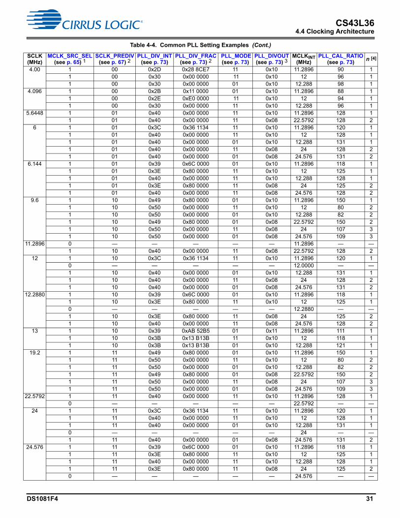
CS43L364.4 Clocking Architecture
4.00 1 00 0x2D 0x28 8CE7 11 0x10 11.2896 90 11 00 0x30 0x00 0000 11 0x10 12 96 11 00 0x30 0x00 0000 01 0x10 12.288 98 1
4.096 1 00 0x2B 0x11 0000 01 0x10 11.2896 88 11 00 0x2E 0xE0 0000 11 0x10 12 94 11 00 0x30 0x00 0000 11 0x10 12.288 96 1
5.6448 1 01 0x40 0x00 0000 11 0x10 11.2896 128 11 01 0x40 0x00 0000 11 0x08 22.5792 128 2
6 1 01 0x3C 0x36 1134 11 0x10 11.2896 120 11 01 0x40 0x00 0000 11 0x10 12 128 11 01 0x40 0x00 0000 01 0x10 12.288 131 11 01 0x40 0x00 0000 11 0x08 24 128 21 01 0x40 0x00 0000 01 0x08 24.576 131 2
6.144 1 01 0x39 0x6C 0000 01 0x10 11.2896 118 11 01 0x3E 0x80 0000 11 0x10 12 125 11 01 0x40 0x00 0000 11 0x10 12.288 128 11 01 0x3E 0x80 0000 11 0x08 24 125 21 01 0x40 0x00 0000 11 0x08 24.576 128 2
9.6 1 10 0x49 0x80 0000 01 0x10 11.2896 150 11 10 0x50 0x00 0000 11 0x10 12 80 21 10 0x50 0x00 0000 01 0x10 12.288 82 21 10 0x49 0x80 0000 01 0x08 22.5792 150 21 10 0x50 0x00 0000 11 0x08 24 107 31 10 0x50 0x00 0000 01 0x08 24.576 109 3
11.2896 0 — — — — — 11.2896 — —1 10 0x40 0x00 0000 11 0x08 22.5792 128 2
12 1 10 0x3C 0x36 1134 11 0x10 11.2896 120 10 — — — — — 12.0000 — —1 10 0x40 0x00 0000 01 0x10 12.288 131 11 10 0x40 0x00 0000 11 0x08 24 128 21 10 0x40 0x00 0000 01 0x08 24.576 131 2
12.2880 1 10 0x39 0x6C 0000 01 0x10 11.2896 118 11 10 0x3E 0x80 0000 11 0x10 12 125 10 — — — — — 12.2880 — —1 10 0x3E 0x80 0000 11 0x08 24 125 21 10 0x40 0x00 0000 11 0x08 24.576 128 2
13 1 10 0x39 0xAB 52B5 01 0x11 11.2896 111 11 10 0x3B 0x13 B13B 11 0x10 12 118 11 10 0x3B 0x13 B13B 01 0x10 12.288 121 1
19.2 1 11 0x49 0x80 0000 01 0x10 11.2896 150 11 11 0x50 0x00 0000 11 0x10 12 80 21 11 0x50 0x00 0000 01 0x10 12.288 82 21 11 0x49 0x80 0000 01 0x08 22.5792 150 21 11 0x50 0x00 0000 11 0x08 24 107 31 11 0x50 0x00 0000 01 0x08 24.576 109 3
22.5792 1 11 0x40 0x00 0000 11 0x10 11.2896 128 10 — — — — — 22.5792 — —
24 1 11 0x3C 0x36 1134 11 0x10 11.2896 120 11 11 0x40 0x00 0000 11 0x10 12 128 11 11 0x40 0x00 0000 01 0x10 12.288 131 10 — — — — — 24 — —1 11 0x40 0x00 0000 01 0x08 24.576 131 2
24.576 1 11 0x39 0x6C 0000 01 0x10 11.2896 118 11 11 0x3E 0x80 0000 11 0x10 12 125 11 11 0x40 0x00 0000 11 0x10 12.288 128 11 11 0x3E 0x80 0000 11 0x08 24 125 20 — — — — — 24.576 — —
Table 4-4. Common PLL Setting Examples (Cont.)
SCLK(MHz)
MCLK_SRC_SEL(see p. 65) 1
SCLK_PREDIV(see p. 67) 2
PLL_DIV_INT(see p. 73)
PLL_DIV_FRAC(see p. 73) 2
PLL_MODE(see p. 73)
PLL_DIVOUT(see p. 73) 3
MCLKINT(MHz)
PLL_CAL_RATIO(see p. 73)
n [4]
DS1081F4 31

CS43L364.4 Clocking Architecture
Powering up the PLL can be accomplished in several configurations. Table 4-4 shows example configurations; the sequences in Section 4.4.3.1 and Section 4.4.3.2 can be used as models.
MCLKINT combinations not shown in Table 4-4 can be determined by Eq. 4-1:
The internal PLL output must be between ~150 and ~300 MHz. The PLL_DIVOUT value must be an even integer. To maximize flexibility in sample-rate choice, MCLKINT must be nominally 12 or 24 MHz.
PLL_CAL_RATIO determines the operating point for the internal VCO. For most configurations, the default value gives proper performance. However, to keep the VCO within range, some scenarios require PLL_CAL_RATIO to be set during the PLL power-up sequence (see Section 4.4.3). Use Eq. 4-2 to calculate the proper VCO setting at PLL start-up:
The value of n in Eq. 4-2 is determined by the following:
• If the result is less than or equal to 151, by default, n equals 1.
• If the result is less than 151, use the result to determine the PLL_CAL_RATIO setting.
• If the result is greater than 151, select another divide factor of n configurations for SCLK (where n = 2,3, …). The result must be between 50 and 151 (see the power-up sequence in Section 4.4.3.2). Use the same n value to multiply PLL_DIVOUT during the power-up sequence; see Step 2 in Section 4.4.3.1. The functional value must be restored (Step 8). The same is shown in both standard examples.
4.4.3.1 PLL Power-Up Sequence (Example: SCLK = 4.096 MHz and MCLKINT = 12.288 MHz)
In this example, SCLK = 4.096 MHz and MCLKINT = 12.288 MHz.
1. Set SCLK_PREDIV to Divide-by-1 Mode (0x00).
2. Set PLL_DIVOUT to Divide-by-16 Mode (0x10). This reflects a value of n = 1, because the PLL_CAL_RATIO generated by Eq. 4-2 equals 96. See that the PLL_DIVOUT entry for this configuration in Table 4-4 used a Divide-by-16 Mode (0x10).
3. Clear the three fractional factor registers, PLL_DIV_FRAC (see Section 7.5.2).
4. Set the integer factor, PLL_DIV_INT to 48 (0x30).
5. Set the PLL Mode multipliers, PLL_MODE to 11 to bypass both 500/512 and 1029/1024 factors (0x03).
6. Set the PLL_CAL_RATIO to 96 (0x60, see Section 7.5.5).
7. Turn on the PLL by setting PLL_START (see p. 72).
8. As part of a standard sequence, after at least 800 s, the PLL_DIVOUT value would need to restored to 16 (0x10), which is unnecessary here because that value did not change.
26 1 11 0x39 0xAB 52B5 01 0x11 11.2896 111 11 11 0x3B 0x13 B13B 11 0x10 12 118 11 11 0x3B 0x13 B13B 01 0x10 12.288 121 1
1. If MCLK_SRC_SEL = 0, the PLL is bypassed and can be powered down by clearing PLL_START (see p. 72). 2. Refer to the register description for the decode. 3. The text following this table explains the use of PLL_DIVOUT, shown by the example configurations in Section 4.4.3.1 and Section 4.4.3.2.4. The variable n represents the divide ratio. See Eq. 4-2.
Equation 4-1. Configuring SCLK, MCLKINT Configurations
MCLKINT = SCLK X
(PLL_DIV_INT + PLL_DIV_FRAC)X
1SCLK_PREDIV (500/512 or 1029/1024 or 1) PLL_DIVOUT
Equation 4-2. Calculating the PLL_CAL_RATIO
PLL_CAL_RATIO = MCLKINT x 32 x SCLK_PREDIV
n x SCLK
Table 4-4. Common PLL Setting Examples (Cont.)
SCLK(MHz)
MCLK_SRC_SEL(see p. 65) 1
SCLK_PREDIV(see p. 67) 2
PLL_DIV_INT(see p. 73)
PLL_DIV_FRAC(see p. 73) 2
PLL_MODE(see p. 73)
PLL_DIVOUT(see p. 73) 3
MCLKINT(MHz)
PLL_CAL_RATIO(see p. 73)
n [4]
DS1081F4 32

CS43L364.4 Clocking Architecture
4.4.3.2 PLL Power-Up Sequence (Example: SCLK = 12 MHz and MCLKINT = 24 MHz)
In this example, SCLK = 12 MHz and MCLKINT = 24 MHz.
1. Set SCLK_PREDIV to Divide-by-4 Mode (0x02).
2. Set PLL_DIVOUT to Divide-by-16 Mode (0x10). This reflects a value of n = 2, because the PLL_CAL_RATIO generated by Eq. 4-2 was greater than 151. See that the PLL_DIVOUT entry for this configuration in Table 4-4 used a Divide-by-8 Mode (0x08).
3. Clear the three fractional factor registers, PLL_DIV_FRAC.
4. Set the integer factor, PLL_DIV_INT to 64 (0x40).
5. Set the PLL mode multipliers, PLL_MODE to 11 to bypass both 500/512 and 1029/1024 factors (0x03).
6. Set the PLL_CAL_RATIO to 128 (0x80).
7. Turn on the PLL by setting PLL_START.
8. After at least 800 s, the PLL_DIVOUT value must be restored from 16 to 8 (0x08).
4.4.3.3 Nonstandard PLL Setting (Example: SCLK = 19.2 MHz and MCLKINT = 12 MHz)
In this example, SCLK = 19.2 MHz and MCLKINT = 12 MHz. (Note that a power-up sequence similar to Section 4.4.3.2 is required for this configuration due to n = 1.)
• SCLK = 19.2 MHz = available reference clock.• MCLKINT = 12 MHz = desired internal MCLK.• SCLK_PREDIV = 11 = divide SCLK by 8 as reference to PLL.• PLL_DIV_INT = 0x50 = multiply reference clock by 80, yielding PLL out = 192 MHz.• PLL_DIV_FRAC = 0x00 0000 = fractional portion equal to zero.• PLL_MODE = 11 = 500/512 and 1029/1024 multipliers are bypassed.• PLL_DIVOUT = 0x10 = divide PLL out by 16 to achieve MCLKINT of 12 MHz.
Table 4-5 shows nonstandard PLL configurations.
As shown in Fig. 4-13, the input to the PLL is the ASP_SCLK input pin.
Table 4-5. Nonstandard PLL Settings
SCLK(MHz)
MCLK_SRC_SEL(see p. 65)
SCLK_PREDIV(see p. 67)
PLL_DIV_INT(see p. 73)
PLL_DIV_FRAC(see p. 73)
PLL_MODE(see p. 73)
PLL_DIVOUT(see p. 73)
MCLKINT(MHz)
PLL_CAL_RATIO(see p. 73)
n [1]
9.6 1 10 0x6E 0x40 0000 01 0x18 11.2896 75 11 10 0x50 0x00 0000 11 0x10 12 80 11 10 0x50 0x00 0000 01 0x10 12.288 82 11 10 0x6E 0x400000 01 0x0C 22.5792 150 11 10 0x50 0x00 0000 11 0x08 24 80 21 10 0x50 0x00 0000 01 0x08 24.576 82 2
19.2 1 11 0x6E 0x40 0000 01 0x18 11.2896 150 11 11 0x50 0x00 0000 11 0x10 12 80 21 11 0x50 0x00 0000 01 0x10 12.288 82 21 11 0x6E 0x40 0000 01 0x0C 22.5792 150 21 11 0x50 0x00 0000 11 0x08 24 107 31 11 0x50 0x00 0000 01 0x08 24.576 109 3
1. The variable n represents the divide ratio. See Eq. 4-2.
Figure 4-13. Clocking Architecture
ASP_SCLK Fractional-N PLL
MCLKINT
VA(+1.8 V)PLL_START
DS1081F4 33

CS43L364.5 Audio Serial Port (ASP)
4.4.3.4 Powering Down the PLL
To power down the PLL, clear PLL_START.
4.5 Audio Serial Port (ASP)
The CS43L36 has an ASP to communicate audio and voice data between system devices, such as application processors and Bluetooth® transceivers. ASP_SCLK_EN (see p. 66) must be set whenever DAI is used. The ASP can be configured to TDM, I2S, and left justified (LJ) audio interfaces.
Note: A maximum of two input channels are supported in TDM Mode.
4.5.1 Slave Mode Timing
The ASP can operate as a slave to another device’s timing, requiring ASP_SCLK and ASP_LRCK/FSYNC to be mastered by the external device. If ASP_HYBRID_MODE is cleared (see p. 66), the serial port acts as a slave. If ASP_HYBRID_MODE is set, the port is in Hybrid-Master Mode (see Section 4.5.2).
In Slave Mode, ASP_SCLK and ASP_LRCK are inputs. Although the CS43L36 does not generate interface timings in Slave Mode, the expected LRCK and SCLK format must be programmed as it is in Hybrid-Master Mode. Table 4-8 shows supported serial-port sample rate examples. Note that some rates require use of the PLL and/or SRC.
4.5.2 Hybrid-Master Mode Timing
In Hybrid-Master Mode, ASP_LRCK is derived from ASP_SCLK; the ASP_SCLK/ASP_LRCK ratio must be N x FS, where N is a large enough integer to support the total number of bits per ASP_LRCK period for the audio stream to be transferred. In either 50/50 Mode or I2S/LJ Mode, the ASP_SCLK/ASP_LRCK ratio must be NE x FS, where NE is an even integer.
The serial port generates an internal LRCK/FSYNC from an externally mastered ASP_SCLK, allowing single clock-source mastering to the CS43L36. In Hybrid-Master Mode, the serial port must provide a left-right/frame sync signal (ASP_LRCK/FSYNC) given an externally generated bit clock (ASP_SCLK).
Table 4-6 shows supported serial-port sample-rate examples. Other rates are possible, but the rules stipulated above must be met. Note that some rates require use of the PLL or SRC.
Table 4-6. Supported Serial-Port Sample Rates
SCLK Frequency (MHz)
Serial Port Sample Rate (kHz)8.0 11.025 11.029 12 16 22.05 22.059 24 32 44.1 44.118 48 88.2 88.235 96 176.4 176.471 192
1.4112 — x — — — x — — — x — — x — — x — —2.8224 — x — — — x — — — x — — x — — x — —5.6448 — x — — — x — — — x — — x — — x — —11.2896 — x — — — x — — — x — — x — — x — —22.5792 — x — — — x — — — x — — x — — x — —
1.024 x — — — x — — — x — — — — — — — — —2.048 x — — — x — — — x — — — — — — — — —4.096 x — — — x — — — x — — — — — — — — —8.192 x — — — x — — — x — — — — — — — — —
2 x — — — x — — — — — — — — — — — — —3 x — x x — — x x — — x — — x — — x —4 x — — — x — — — x — — — — — — — — —6 x — x x x — x x — — x x — x — — x —
12 x — x x x — x x x — x x — x x — x —24 x — x x x — x x x — x x — x x — x x
1.536 x — — x x — — x x — — x — — x — — x3.072 x — — x x — — x x — — x — — x — — x6.144 x — — x x — — x x — — x — — x — — x
12.288 x — — x x — — x x — — x — — x — — x24.576 x — — x x — — x x — — x — — x — — x
9.6 x — — x x — — x x — — x — — x — — x19.2 x — — x x — — x x — — x — — x — — x
DS1081F4 34

CS43L364.5 Audio Serial Port (ASP)
Fig. 4-14 and Fig. 4-15 show the serial-port clocking architectures.
Figure 4-14. ASP SCLK Architecture
Figure 4-15. ASP LRCK Architecture
As shown in Fig. 4-16, the LRCK period (FSYNC_PERIOD_LB and FSYNC_PERIOD_UB, see p. 66) controls the number of SCLK periods per frame. This effectively sets the frame length and the number of SCLK periods per Fs. Frame length may be programmed in single SCLK period multiples from 16 to 4096 SCLK:Fs. If ASP_HYBRID_MODE (see p. 66) is set, the SCLK period multiples must be set to 2 * n * Fs, where n {8, 9, …, 2048}.
Figure 4-16. ASP LRCK Period, High Width
FSYNC_PULSE_WIDTH_LB and FSYNC_PULSE_WIDTH_UB (see p. 65) control the number of SCLK periods for which the LRCK signal is held high during each frame. Like the LRCK period, the LRCK-high width is programmable in single SCLK periods, from at least one period to at most the LRCK period minus one. That is, the LRCK-high width must be shorter than the LRCK period.
As shown in Fig. 4-17, if 50/50 Mode is enabled (ASP_5050 = 1, see p. 67), the LRCK high duration must be programmed to the LRCK period divided by two (rounded down to the nearest integer when the LRCK period is odd). When the serial port is in 50/50 Mode, setting the LRCK high duration to a value other than half of the period causes erroneous operation.
CLK DIVIN
DIVSEL
OUTSCLKTo LRCK_GEN
SCLK in to DAI CLKGENASP_SCLK 0
1
MCLKDIVp. 65
ASP_SCPOL_IN_DAC p. 66
ASP_SCLK_EN = 1 (See p. 66)
LRCK in
ASP_LRCK/FSYNC
0
1
LR Generation
IN
PER
OUT
HI
EN
From SCLK
5050
DELAY
0
1
ASP_LCPOL_OUT p. 66
FSYNC_PULSE_WIDTH_LB p. 65FSYNC_PULSE_WIDTH_UB p. 65
FSYNC_PERIOD_LB p. 66,FSYNC_PERIOD_UB p. 66
ASP_5050 p. 67
ASP_FSD p. 67
ASP_LCPOL_IN p. 66
ASP_HYBRID_MODE p. 66
ASP_HYBRID_MODE p. 66
SCLK
LRCK
Falling Edge
Rising Edge
FSYNC_PERIOD
FSYNC_PULSE_WIDTH
...
...
...
...
...
...
DS1081F4 35

CS43L364.5 Audio Serial Port (ASP)
Figure 4-17. ASP LRCK Period, High Width, 50/50 Mode
Fig. 4-18 shows how LRCK frame start delay (ASP_FSD, see p. 67) controls the number of SCLK periods from LRCK synchronization edge to the start of frame data.
4.5.3 Channel Location and Resolution
Each serial-port channel’s location and offset is configured through the registers in Table 4-7. Location is programmable in single SCLK-period resolution. If set to the minimum location offset, a channel sends or receives on the first SCLK period of a new frame. Channel size is programmable in 8- to 32-bit byte resolutions. DAC ports are limited to 24 bits and truncate the 8 LSBs of a 32-bit audio stream.
Figure 4-18. LRCK FSD and SCLK Polarity Example Diagram
SCLK
LRCK
Falling Edge
Rising Edge
FSYNC_PERIOD
FSYNC_PULSE_WIDTH
SCLK
LRCK
Falling Edge
Rising Edge
FSYNC_PERIOD
FSYNC_PULSE_WIDTH
Even FSYNC_PERIOD
Odd FSYNC_PERIOD FSYNC_PERIOD count clock is absent
FSYNC_PULSE_WIDTH
...
...
...
...
...
...
...
...
...
...
...
...
LRCK
0 1
Channel location and size
FSD = 000
FSD = 001
FSD = 010
N-1N-2N-3N-4N-5
FSD = 011
0
FSD = 100
0.511.522.5
FSD = 101
End of frame
2 ...
...
...
...
...
...
...
3 4 5 6 7 8 9
...
0 1 N-1N-2N-3N-4N-5
End of frame
2 ...3 4 5 6 7 8 9
...SCLK
SDIN
SCLK
SDIN
Channel location and size
ASP_SCPOL_IN_DAC (SDIN) = 0
ASP_SCPOL_IN_DAC (SDIN) = 1
DS1081F4 36

CS43L364.5 Audio Serial Port (ASP)
Channel size and location must not be programmed such that channel data exceeds the frame boundary. In other words, channel size and offset must not exceed the expected SCLK per LRCK settings. Size and location must not be programmed such that data from a given SCLK period is assigned to more than one channel. However, an exception exists for the DAI as the same data can be used for both received channels’ location, if desired. For an example, see Section 5.1.
Fig. 4-19 shows channel location and size. See ASP_RX0_2FS (p. 79).
Figure 4-19. Example Channel Location and Size
4.5.4 Isochronous Serial-Port Operation
In Isochronous Mode, audio data can be transferred between the internal audio data paths and a serial port at isochronous frequencies slower than the LRCK frequency. In all cases, the sample rate/LRCK frequency ratio must be one for which there are points at which rising edges regularly align.
Notes: Combining an isochronous audio stream on a channel (or on multiple channels) concurrently with a native audiostream on another channel (or other multiple channels) is not supported.
In Isochronous Mode, if a stream’s sample rate does not match the LRCK frequency, it must include nulls, indicated by the negative full-scale (NFS) code (1 followed by 0s) or by adding nonaudio bits (NSB Mode) to the data stream.
SP_RX_NFS_NSBB (see p. 78) selects between the NFS and NSB modes.In NFS Mode, to achieve a desired isochronous output sample rate, a null-insert block adds NFS samples to the output stream. NFS samples input to the null-insert block are incremented and are passed to the output as valid, nonnull samples.
In NSB Mode, a null-insert block adds 8 bits to the data stream and inserts null samples to achieve a desired isochronous output sample rate. Inserted null samples are defined as NFS including the nonaudio bits. NFS samples that are input to the null-insert block are passed as valid, nonnull samples to the output. Valid samples are indicated by a nonzero value in the null sample indicator bit. The null sample indicator bit is globally defined by the SP_RX_NSB_POS (see p. 78). Total data stream sample width, including the nonaudio bits, is N + 8 bits. Therefore, the maximum HD audio sample width is 24 bits in NSB Mode.
In NFS Mode, a null-remove block deletes null samples, restoring the stream’s original sample rate. NFS samples that are input to the null-remove block are removed from the data stream as invalid, null samples.
In NSB Mode, a null-remove block deletes samples that have a zero null sample indicator bit, restoring the stream’s original sample rate. Furthermore, the output data has the least-significant 8 bits of nonaudio data removed. Samples with a zero null sample indicator bit are removed from the data stream as invalid, null samples.
In either NSB or NFS Mode, setting the Rx rate fields (SP_RX_FS, see p. 79) matters only if an isochronous mode is selected via SP_RX_ISOC_MODE (see p. 78). Supported isochronous rates are 48k, 96k, and 192k. The ASPx Rx rate bits are used only to help determine when to remove nulls and to provide the correct fSI/fSO to the SRCs while in Isochronous Mode.
Table 4-7. ASP Channel Controls
Channel Resolution MSB Location LSB LocationASP Receive DAI0 Channel 1 ASP_RX0_CH1_RES ASP_RX0_CH1_BIT_ST_MSB ASP_RX0_CH1_BIT_ST_LSBASP Receive DAI0 Channel 2 ASP_RX0_CH2_RES ASP_RX0_CH2_BIT_ST_MSB ASP_RX0_CH2_BIT_ST_LSB
Slot 0
SCLK
Slot 1 Slot 62 Slot 63
0503
504 511
7 0 7 0 7 0
First SCLK latching edge of a new frame after frame sync
Traditional ‘Slot’
N
23 Ch. M MSB Ch. M LSB 0
15 Ch. M MSB Ch. M LSB 0
7 Ch. M MSB 0Channel Resolution = 00
Channel Resolution = 01
Channel Resolution = 10
Channel Location = N
TDM Channel M Data
Don’t Care
Don’t Care
7
DS1081F4 37

CS43L364.5 Audio Serial Port (ASP)
For null-remove operations, the rates do not need to match the actual data rate. Likewise, if data is being or captured at its native rate, these registers have no effect.
As Fig. 4-20 shows, the null-sample bit (NSB) flag may be any bit of the least-significant sample byte. NSB-encoded streams are assumed to contain 8 bits of nonaudio data as the LSB.
Figure 4-20. NSB Null Encoding
To send isochronous audio data to a serial port, the data pattern must be such that the LRCK/FSYNC transition preceding any given nonnull sample on the 48-kHz serial port does not deviate by more than one sample period from a virtual clock running at the desired sample rate. Use the following example to determine the data word as it appears on the serial port.
error = 0for each LRCK
if(error < 1/FLRCK)output = <<next sample>>error = error + (1/Fs - 1/FLRCK)
elseoutput = NULLerror = error - 1/FLRCK
The null-sample sequences in Table 4-8 result from the example above for common sample rates. This method ensures that the internal receive data FIFO does not underrun or overrun, which would cause audio data loss. Depending on the internal audio data FIFOs’ startup conditions and on the serial-port clock-phase relationships, isochronous data sent from a serial port may not adhere to the data patterns in Table 4-8. In all cases, the transmitted audio data rate matches the stream sample rate.
4.5.5 50/50 Mode
Regardless of the state of ASP_LRCK/FSYNC, in 50/50 Mode (ASP_5050 = 1, see p. 67), the ASP can start a frame.
The ASP_STP setting (see p. 67) determines which LRCK/FSYNC phase starts a frame in 50/50 Mode, as follows:
Table 4-8. Isochronous Input Data Pattern Examples
Sample Rate (kHz) Isochronous Data Pattern for LRCK = 48 kHz8.000 1S5N (repeat)11.025 [[[1s3nx2]1s4n]x5 1s3n1s4n]x4 [[1s3nx2]1s4n]x4 1s3n1s4n [[[1s3nx2]1s4n]x5 1s3n1s4n]x3
[[1s3nx2]1s4n]x4 1s3n1s4n (repeat)12.000 1S3N (repeat)16.000 1S2N (repeat)22.05 [[1s1nx6]1n [1s1nx6]1n [1s1nx5]1n]x8 [1s1nx6]1n [1s1nx5]1n (repeat)
24.000 1S1N (repeat)32.000 2S1N (repeat)44.100 [12s1n[11s1n]x2]x3 11s1n (repeat)48.000 1S (repeat)
Note: N = Null sample, S = Normal sample
ISO null sample indicator bit (selectable, Non‐PCM)1: Normal sample0: Null sampleOther bits are ignored
N 0Audio Sample
0N + 8
DS1081F4 38

CS43L364.5 Audio Serial Port (ASP)
• If ASP_STP = 0, the frame begins when LRCK/FSYNC transitions from high to low. See Fig. 4-21.
• If ASP_STP = 1, the frame begins when LRCK/FSYNC transitions from low to high. See Fig. 4-22.
In 50/50 Mode, left and right channels are programmed independently to output when LRCK/FSYNC is high or low—that is, the channel-active phase. The active phase is controlled by ASP_RXx_CHy_AP (see Section 7.14). If x_AP = 1, the respective channel is output if LRCK/FSYNC is high. If x_AP = 0, the channel is output if LRCK/FSYNC is low.
Note: Active phase has no function if 50/50 Mode = 0 or ASP_RX1_2FS = 1.
In 50/50 Mode, the channel location (see Section 4.5.3) is calculated within the channel-active phase. If there are N bits in a frame, the location of the last bit of each active phase is equal to (N/2) – 1.
4.5.6 Serial Port Status
Each serial port has sticky, write-1-to-clear status bits related to capture paths. These bits are described in Section 7.4.3. Mask bits (Section 7.4.12) determine whether INT is asserted when a status bit is set. Table 4-9 provides an overview.
Figure 4-21. Example 50/50 Mode (ASP_STP = 0)
Figure 4-22. Example 50/50 Mode (ASP_STP = 1)
Table 4-9. Serial Port Status
Name Direction Description Register Reference
Request Overload
Rx Set when too many input buffers request processing at the same time. If all channel registers are properly configured, this error status should never be set.
ASPRX_OVLD p. 68
LRCK Error Rx Logical OR of LRCK Early and LRCK Late (see below). ASPRX_ERROR p. 68
LRCK Early Rx Set when the number of SCLK periods per LRCK phase (high or low) is less than the expected count as determined by x_LCPR and x_LCHI.Note: The Rx LRCK early interrupt status is set during the first receive LRCK early event. Subsequent receive LRCK early events are indicated only if valid LRCK transitions are detected.
ASPRX_EARLY p. 68
LRCK Late Rx Set when the number of SCLK periods per LRCK phase (high or low) is greater than the expected count as determined by x_LCPR and x_LCHI.
ASPRX_LATE p. 68
No LRCK Rx Note: Set when the number of SCLK periods counted exceeds twice the value of LRCK period (x_LCPR) without an LRCK edge.
ASPRX_NOLRCK p. 68
LRCK ...
...x_STP = 0
SCLK ... ...
Channel y Channel z Next SamplePrevious Sample
x_CHy_LOC = 0, x_CHy_AP = 0 x_CHz_LOC = 0, x_CHz_AP = 1SDIN
Channel z Channel y Next SamplePrevious Sample
x_CHz_LOC = 0, x_CHz_AP = 0 x_CHy_LOC = 0, x_CHy_AP = 1This diagram assumes x_FSD = 0
0 1 2Channel location index x_CHy_LOC, x_CHz_LOC) N/2 – 1N/2 – 2N/2 – 3... 0 1 2 N/2 – 1N/2 – 2N/2 – 3...
LRCK
SCLK ... ...
Channel y Channel z Next SamplePrevious Sample
x_CHy_LOC = 0, x_CHy_AP = 1 x_CHz_LOC = 0, x_CHz_AP = 0SDIN
Channel z Channel y Next SamplePrevious Sample
x_CHz_LOC = 0, x_CHz_AP = 1 x_CHy_LOC = 0, x_CHy_AP = 0
...
...x_STP = 1
0 1 2Channel location index (x_CHy_LOC, x_CHz_LOC) N/2 – 1N/2 – 2N/2 – 3... 0 1 2 N/2 – 1N/2 – 2N/2 – 3...
DS1081F4 39

CS43L364.6 Sample-Rate Converters (SRCs)
4.5.7 Recommended Serial-Port Power-Up and Power-Down Strategies
Although multiple safeguards and controls are implemented to prevent a run on the FIFOs involved in passing data from the input port to the output port, the following power-up sequence is recommended. Section 5 gives detailed sequences.
1. Configure all playback channel characteristics—bit resolution, channel select, source (DAI), native/isochronous, sample rates, etc.
2. Power up playback, and ASRCs.
3. Release the PDN_ALL bit.
4. Power up the serial ports (DAI).
The following power-down sequence is recommended:
1. Power down the playback path.
2. Power down the serial ports.
4.6 Sample-Rate Converters (SRCs)
SRCs bridge different sample rates at the serial ports within the digital-processing core. SRCs are used for the following:
• Two ASP input channels (Channels 1 and 2).
• SRCs are bypassable by setting SRC_BYPASS_DAC (see p. 61).
An SRC’s digital-processing side (as opposed to its serial-port side) connects to the DAC. Multirate DSP techniques are used to up-sample incoming data to a very high rate and then down-sample to the outgoing rate. Internal filtering is designed so that a full-input audio bandwidth of 20 kHz is preserved if the input and output sample rates are at least 44.1 kHz. If the output sample rate becomes less than the input sample rate, the input is automatically band limited to avoid aliasing artifacts in the output signal.
The following restrictions must be met:
• The Fso-to-FSI ratio must be no more than 1:6 or 6:1. For example, if the DAC is at 48 kHz, the input to the SRC must be at least 8 kHz.
• SRC operation cannot be changed on-the-fly. Before changing the SRC operation (e.g., changing SRC frequencies or bypassing or adding the SRCs), the user must follow the power sequences provided in Section 4.5.7.
• The MCLK frequency must be as close as possible to, but not less than the minimum SRC MCLK frequency, MCLKMIN, which must be at least 125 times the higher of the two sample rates (FSI or Fso).
For example, if Fso is 48 kHz and FSI is 32 kHz, the MCLK must be as close as possible to, but not less than, an MCLKMIN of 6.0 MHz. The MCLK frequency for the SRCs is configured through CLK_IASRC_SEL (see p. 67).
Table 4-10 shows settings for the supported sample rates and corresponding MCLKINT frequencies.
Jitter in the incoming signal has little effect on rate-converter dynamic performance. It does not affect the output clock.
A digital PLL continually measures the heavily low-pass-filtered phase difference and the frequency ratio between input and output sample rate clocks. It uses the data to dynamically adjust coefficients of a linear time-varying filter that processes a synchronously oversampled version of the input data. The filter output is resampled to the output sample rate.
For input serial ports, input and output sample-rate clocks are respectively derived from the external serial-port sample clock (x_LRCK) and the internal Fs clock. FS_EN (see p. 67) must be set according to the FSI or Fso SRC sample rates.
Table 4-10. Supported Sample Rates and Corresponding MCLKINT Encodings
Fsint(kHz)
Serial Port Sample Rate (kHz) 8.0 11.025 11.029 12 16 22.05 22.059 24 32 44.1 44.118 48 88.2 88.235 96 176.4 176.471 192
44.1 00 00 00 00 00 00 00 00 00 00 00 00 01 01 01 10 10 1048 00 00 00 00 00 00 00 00 00 00 00 00 01 01 01 10 10 10
Note: SRC MCLKINT Freq= 00 (6 MHz), 01 (12 MHz), 11 (24 MHz), configured in CLK_IASRC_SEL (see p. 67)
DS1081F4 40

CS43L364.7 Headset Interface
Minimize the SRCs’ lock time by programming the serial-port interface sample rates into the x_FS registers (see Section 7.13.1). If the rates are unknown, programming these registers to “don’t know” would likely increase lock times. Proper operation is not assured if sample rates are misprogrammed.
4.7 Headset Interface
Split digital-power domains (VD_FILT and VP) within the headset interface support an ultralow-power standby mode where only the VP supply is used. An output signal may be used to tell the system to wake from its low-power state when a headset plug is inserted or removed. The interface may be reset by three types of resets with progressively less effect.
Figure 4-23. Headset Interface Block Diagram
The control port includes registers that source individually maskable interrupts. Event-change debouncing is used to filter applicable status registers. Latchable duplicate registers are used to pass information to the Standby Mode supply domain.
4.8 Plug Presence Detect
The CS43L36 uses TIP_SENSE to detect plug presence. The sense pin is debounced to filter out brief events before being reported to the corresponding presence-detect bit and generating an interrupt if appropriate.
4.8.1 Plug Types
The CS43L36 supports the following industry-standard plug types:
• Tip–Ring–Sleeve (TRS)—Consists of a segmented metal barrel with the tip connector used for HPOUTA, a ring connector used for HPOUTB, and a sleeve connector used for HSGND.
• Tip–Ring–Ring–Sleeve (TRRS)—Like TRS, with an additional ring connector for the mic connection. There are two common pinouts for TRRS plugs:
— One uses the tip for HPOUTA, the first ring for HPOUTB, the second ring for HSGND, and the sleeve for mic.
— The CS43L36 does not support OMTP, or China, headset, which swaps the third and fourth connections, so that the second ring carries mic and the sleeve carries HSGND.
4.8.2 Tip-Sense Methods
The following methods are used to detect the presence or absence of a plug:
• Tip sense (TS)—A sense pin is connected to a terminal on the receptacle such that, if no plug is inserted, the pin is floating. If a plug is inserted, the pin is shorted to the tip (T) terminal. The tip is sensed by having a small current source in the device pull up the pin if it is left floating (no plug). If a plug is inserted and the sense pin is shorted to HPOUTA, the sense
TIP_SENSE
–VCP_FILT GND
VA VP
Plug Detect
Headset Interface
Step-Down,Inverting Charge
Pump Control Port
INT
WAKE
RESET
VA VP
–VCP_FILT GND
RESET
LDO Regulatorand POR Generator
VL
Power On Reset
ControlPort
VL
Logic
RESET
Level Shifters
VD_FILT
VD_FILT
DS1081F4 41

CS43L364.8 Plug Presence Detect
pin is assumed to be pulled low via clamps at the HP amp output when it is in power down. If the HP amp is running, the sense pin is shorted to the output signal and, therefore, is pulled below a certain threshold via the output stage of the HP amp. Thus, a low level at the sense pin indicates plug inserted, and a high level at the sense pin indicates plug removed.
• Inverted tip sense (ITS)—Like tip sense, but with a connector whose sense pin is shorted to the tip terminal if the plug is removed and is left floating if it is inserted. Therefore, a low level at the sense pin indicates plug removed and a high level at the sense pin indicates plug inserted. Inversion is controlled by the following:
— The invert (TIP_SENSE_INV, p. 75), which goes to the analog and affects a number of other features.
— The tip-sense invert (TS_INV, p. 64), which affects only the configuration bits in Section 6.2.
4.8.3 Tip-Sense Debounce Settings
Fig. 4-24 shows the tip-sense controls and the associated interrupt, status, and mask registers.
Figure 4-24. Tip-Sense Controls
The tip-sense debounce register fields behave and interact as follows:
• TS_UNPLUG_DBNC. Shows tip sense status after being unplugged with the associated debounce time.
• TS_PLUG_DBNC. Shows tip sense status after being plugged in with the associated debounce time.
Note: TS_INV must be set to have TS_PLUG/TS_PLUG_DBNC status match TIP_SENSE_PLUG status.
The debounce bits are described in Section 7.2.7. Multiple debounce settings can be configured for insertion, removal, and tip sense:
• TIP_SENSE_DEBOUNCE (see p. 75) controls the tip-sense removal debounce time.
• TS_FALL_DBNCE_TIME and TS_RISE_DBNCE_TIME (see p. 64) settings configure the corresponding debounce times.
4.8.4 Setup Instructions
The following steps are required to activate the tip-sense debounce interrupt status:
1. Clear PDN_ALL (see p. 63).
2. Set LATCH_TO_VP (see p. 75) to latch analog controls into analog circuits.
3. Write TIP_SENSE_CTRL (see p. 75) to 01 or 11 to enable debounce for tip sense plug/unplug.
4. Clear interrupt masks (0x1320, see Section 7.4.17).
Interrupt status (see Section 7.4.9) does not contain an event-capture latch—a read always yields the current condition.
TIP_SENSE 0
1
0
1
Interrupt (0x1B7B)Mask (0x1B79)
Headset Interface Block
No Delay
Rising/Falling Edge Detect
Tip Sense Indicator Status Registers (0x1115)
Tip SensePlug/Unplug Interrupt
Mask (0x1320)
Tip SensePlug/Unplug Interrupt
Status (0x130F)
Interrupt Handler Block
Shadow Copy
INT
Read Clears INT
UNPLUG
PLUG
No Delay
TIP_SENSE_PLUG p. 69TIP_SENSE_UNPLUG p. 69
TIP_SENSE_DEBOUNCE p. 75
TS_FALL_DBNCE_TIME p. 64
TS_RISE_DBNCE_TIME p. 64
TIP_SENSE p. 76
TS_INV p. 64TIP_SENSE_INV. p. 75
TS_UNPLUG_DBNCp. 65TS_PLUG_DBNCp. 65
TS_UNPLUG p. 70TS_PLUG p. 70
M_TS_UNPLUG p. 72 M_TS_PLUG p. 72
DS1081F4 42

CS43L364.9 Power-Supply Considerations
Table 4-11 describes the plug/unplug status.
4.9 Power-Supply Considerations
Because some power supply combinations can produce unwanted system behavior, note the following:
• Control-port transactions can occur 1 ms after VP, VD_FILT, VCP, and VL exceed the minimum operating voltage.
• If VP supply is off, it is recommended that all other supplies are also off. VP must be the first supply turned on.
• RESET must be asserted until VP is valid.
• If VD_FILT is supplied externally (DIGLDO_PDN = GND), VL must be supplied before VD_FILT, VA, VL, and VCP can come up in any order. Due to the VD_FILT POR, VD_FILT must be turned off before VA, VL, or VCP are turned off; otherwise, current could be drawn from supplies that remain on.
Table 4-12 shows the maximum current for each supply when VP is on, but other supplies are on or off (all clocks are off and all registers are set to default values, i.e., reset).
Table 4-13 shows requirements and available features for valid power-supply configurations.
4.9.1 VP Monitor
The CS43L36 voltage comparator monitors the VP power supply for potential brown-out conditions due to power-supply overload or other fault conditions. To perform according to specifications, VP is expected to remain above 3.0 V at all times. The VP monitor is enabled by setting VPMON_PDNB (see p. 64) and must be powered up after VP is above 3.0 V
Table 4-11. Tip Plug/Unplug Status
Plug Status Unplug Status Interpretation0 0 Tip is fully unplugged/not present1 0 Reserved0 1 Tip connection is in a transitional state1 1 Tip is fully plugged/present
Table 4-12. Typical Leakage Current during Nonoperational Supply States (with VP Powered On)
Supply Current (µA)Notes
VCP VA VL IVp IVCP IVA IVLOff On Off 14 0 0 0 VA may source or sink currentOff On On 25 0 0 328 VA may source or sink currentOn Off Off 14 0 0 0 —On Off On 25 0 0 328 —On On Off 14 0 0 0 VA may source or sink currentOn On On 25 0 0 328 —
Notes: • Values shown reflect typical voltage and temperature. Leakage current may vary by orders of magnitude across the maximum and minimum recommended operating supply voltages and temperatures listed in Table 3-2.
• Test conditions: Clock/data lines are held low, RESET is held high, and all registers are set to their default values.
Table 4-13. Valid Power-Supply Configurations
Configuration NotesOn: VPOff: VD_FILT = VCP = VL = VA
Limited set of headset plug-detect and WAKE output features, see Section 4.7 and Section 4.8.
On: VP = VLOff: VD_FILT = VCP = VA = OFF
Limited set of headset plug-detect and WAKE output features, see Section 4.7 and Section 4.8. Digital I/O ESD diodes are powered to prevent conduction in pin-sharing applications.
On: VP = VD_FILT = VCP = VL = VA Full chip functionality
DS1081F4 43

CS43L364.9 Power-Supply Considerations
to eliminate erroneous faulty condition detection. Fig. 4-25 shows the behavior of the VP monitor.
Figure 4-25. VP Monitor
The following describes the VP monitor behavior with respect to the voltage level:
• If VP drops below 3.0 V, TIP_SENSE performance may be compromised.
• If VP drops below 2.6 V, the VPMON_TRIP status bit is set (see p. 69). An interrupt is triggered if M_VPMON_TRIP = 0 (see p. 72). This bit must be unmasked/enabled only if VP is above the detection-voltage threshold. It must be masked/disabled by default to eliminate erroneous interrupts while VP is ramping or is known to be below the threshold voltage.
• A brown-out condition remains until VP returns to a voltage level above 3.0 V.
• The VP monitor circuit becomes unreliable at VP levels below 2.4 V as it may trigger a power-on reset sequence by the device.
• The VP monitor is intended to detect slow transitioning signals about the 2.6-V threshold. Pulses of short duration are filtered by the monitor and may not trigger at the 2.6-V threshold, but at a value much lower than expected.
VPMON_TRIP
2.6 V
3.0 V
3.6 V
DS1081F4 44

CS43L364.10 Control-Port Operation
4.10 Control-Port Operation
Control-port registers are accessed through the I2C interface, allowing the DAC to be configured for the desired operational modes and formats.
4.10.1 I2C Control-Port Operation
The I2C control port can operate completely asynchronously with the audio sample rates. However, to avoid interference problems, the I2C control port pins must remain static if no operation is required.
The control port uses the I2C interface, with the DAC acting as a slave device. The I2C control port can operate in the following modes, which are configured through the I2C debounce register in Section 7.1.9:
• Standard Mode (SM), with a bit rate of up to 100 kbit/s
• Fast Mode (FM), with a bit rate of up to 400 kbit/s
• Fast Mode Plus (FM+), with a bit rate of up to 1 Mbit/s.
Note: ASP_SCLK is not required to be on when the control port is accessed, for state machines affected by register settings to advance.
SDA is a bidirectional data line. Data is clocked into and out of the CS43L36 by the SCL clock. Fig. 4-26–Fig. 4-29 show signal timings for read and write cycles. A Start condition is defined as a falling transition of SDA while the clock is high. A Stop condition is defined as a rising transition of SDA while the clock is high. All other SDA transitions occur while the clock is low.
The register address space is partitioned into 8-bit page spaces that each comprise up to 127 8-bit registers. Address 0x00 of each page is reserved as the page indicator, PAGE. Writing to address 0x00 of any page changes the page pointer to the address written to address 0x00.
To initiate a write to a particular register in the map, the page address, 0x00, must be written following the chip address. Subsequent accesses to register addresses are treated as offsets from the page address written in the initial transaction. To change the page address, initiate a write to address 0x00. To determine which page is active, read address 0x00.
Figure 4-26. Control-Port Timing, I2C Write of Page Address
The first byte sent to the CS43L36 after a Start condition consists of a 7-bit chip address field and a R/W bit (high for a read, low for a write) in the LSB. To communicate with the CS43L36, the chip address field must match 1_0010, followed by the state of the AD1 and AD0 pins.
Note: Because AD0 and AD1 logic states are latched at POR, dynamic addressing is not supported.
If the operation is a write, the next byte is the memory address pointer (MAP); the 7 LSBs of the MAP byte select the address of the register to be read or written to next. The MSB of the MAP byte, INCR, selects whether autoincrementing is to be used (INCR = 1), allowing successive reads or writes of consecutive registers.
Each byte is separated by an acknowledge (ACK) bit, which the CS43L36 outputs after each input byte is read and is input to the CS43L36 from the microcontroller after each transmitted byte.
4 5 6 7 24 25 26 27
SCL
CHIP ADDRESS (WRITE) MAP BYTE DATA
START STOP
ACK
SDA 7 6 1 0
0 1 2 3 8 9 12 16 17 18 19 10 11 13 14 15
SDASource
Master Master Master
Pullup
Slave Slave
Master
Pullup
ACK ACK
7 6 5 4 3 2 1 0
MAP Addr = 0
INC
R =
0
7 6 5 4 3 2 1 0
R/W
= 0
Slave
Add
r D
ata
to
Add
r 0Addr = 10010
AD
0
AD
1
DS1081F4 45

CS43L364.10 Control-Port Operation
For write operations, the bytes following the MAP byte are written to the CS43L36 register addresses pointed to by the last received MAP address, plus however many autoincrements have occurred. Note that, while writing, any autoincrementing block accesses that go past the maximum 0x7F address write to address 0x00—the page address. The writes then continue to the newly selected page. Fig. 4-27 shows a write pattern with autoincrementing.
Figure 4-27. Control-Port Timing, I2C Writes with Autoincrement
For read operations, the contents of the register pointed to by the last received MAP address, plus however many autoincrements have occurred, are output in the next byte. While reading, any autoincrementing block access that goes past the maximum 0x7F address wraps around and continues reading from the same page address. Fig. 4-28 shows a read pattern following the write pattern in Fig. 4-27. Notice how read addresses are based on the MAP byte from Fig. 4-27.
Figure 4-28. Control-Port Timing, I2C Reads with Autoincrement
To generate a read address not based on the last received MAP address, an aborted write operation can be used as a preamble (see Fig. 4-29). Here, a write operation is aborted (after the ACK for the MAP byte) by sending a Stop condition.
4 5 6 7 24 25
SCL
CHIP ADDRESS (WRITE) MAP BYTE DATA DATA
START STOP
ACKACK
SDA 7 6 1 0
0 1 2 3 8 9 12 16 17 18 19 10 11 13 14 15 27 2826
DATA
SDASource
Master Master Master
Pullup
Slave Slave Slave Slave
Master
Pullup
ACK ACK
7 6 5 4 3 2 1 0
MAP Addr = X
INC
R =
1
7 6 5 4 3 2 1 0
R/W
= 0
Da
ta to
Ad
dr X
+1
Da
ta to
Ad
dr X
+n
Master Master
Slave
Dat
a to
Add
r X
7 6 1 0 7 6 1 0
Addr = 10010
AD
0
AD
1
SCL
SDA
SDASource
Pullup
DATA
STOPACK
ACK
7 0 7 0
CHIP ADDRESS (READ)
START
7 0
NO
258 9 184 5 6 7 0 1 2 3 16 17 34 35 36
ACK
7 6 5 4 3 2 1 0
R/W
= 1
DATA DATA
Dat
a fr
om
Add
r X
+n+1
Dat
a fr
om
Add
r X
+n+2
Dat
a fr
om
Add
r X
+n+3
Master Slave Slave Slave
Master Master Master Pullup
27
Addr = 10010
AD
0
AD
1
DS1081F4 46

CS43L364.11 Reset
Figure 4-29. Control-Port Timing, I2C Reads with Preamble and Autoincrement
The following pseudocode illustrates an aborted write operation followed by a single read operation, assumes page address has been written. For multiple read operations, autoincrement would be set to on (as shown in Fig. 4-29).
Send start condition.Send 10010(AD1)(AD0)0 (chip address and write operation).Receive acknowledge bit.Send MAP byte, autoincrement off.Receive acknowledge bit.Send stop condition, aborting write.Send start condition.Send 10010(AD1)(AD0)1 (chip address and read operation).Receive acknowledge bit.Receive byte, contents of selected register.Send acknowledge bit.Send stop condition.
4.11 Reset
The CS43L36 offers the reset options described in Table 4-14.
4.12 Interrupts
The following sections describe the CS43L36 interrupt implementation.
4.12.1 Standard Interrupts
The interrupt output pin, INT, is used to signal the occurrence of events within the device’s interrupt status registers. Events can be masked individually by setting corresponding bits in the interrupt mask registers. Table 4-15 lists interrupt status and mask registers. The configuration of mask bits determines which events cause the immediate assertion of INT:
• When an unmasked interrupt status event is detected, the status bit is set and INT is asserted.
• When a masked interrupt status event is detected, the interrupt status bit is set, but INT is not affected.
Once asserted, INT remains asserted until all status bits that are unmasked and set have been read. Interrupt status bits are sticky and read-to-clear: Once set, they remain set until the register is read and the associated interrupt condition is not present. If a condition is still present and the status bit is read, although INT is deasserted, the status bit remains set.
Table 4-14. Reset Summary
Reset Cause Result
Device hard reset Asserting RESET If RESET is asserted, all registers (both VP and VD_FILT domains) and all state machines are immediately set to their defaults. No operation can begin until RESET is deasserted. Before normal operation can begin, RESET must be asserted at least once after the VP supply is first brought up.
Power-on reset (POR) Power up If VD_FILT is lower than the POR threshold, the VD_FILT register fields and the state machines are held in reset, setting them to their default values/states. This does not reset the VP registers. The POR releases the reset when the VD_FILT supply goes above the POR threshold. VL and VA supplies must be turned at the same time the VD_FILT supply is turned on.
SCL
CHIP ADDRESS (WRITE) MAP BYTE DATA
STARTACK
STOPACK
ACKACK
SDA 7 0 7 0
CHIP ADDRESS (READ)
START
7 6 5 4 3 2 1 0 7 0
NO
16 8 9 12 13 14 15 4 5 6 7 0 1 20 21 22 23 24 26 27 28 2 3 10 11 17 18 19 25
ACK
STOP
MAP Addr = Z
INC
R =
1Addr = 10010
7 6 5 4 3 2 1 0
R/W
= 0
7 6 5 4 3 2 1 0
R/W
= 1
DATA DATA
Dat
a fr
om
Ad
dr Z
Dat
a fr
om
Ad
dr Z
+1
Dat
a fr
om
Ad
dr Z
+n
SDASource
Master Master Master
Pullup
Slave Slave
Slave Slave Slave
Master Master Master
Pullup
AD
0
AD
1 Addr = 10010
AD
0
AD
1
DS1081F4 47

CS43L364.13 FILT+ Operation
To clear status bits set due to initiation of a path or block, the status bits must be read after the corresponding module is enabled and before normal operation begins. Otherwise, unmasking previously set status bits causes assertion of INT.
As Table 4-16 indicates, interrupt sources are categorized into two groups:
• Condition-based interrupt source bits are set when the condition is present and they remain set until the register is read and the condition that caused the bit to assert is no longer present.
• Event-based interrupt source bits are cleared when read. In the absence of subsequent source events, reading one of these status bits returns a 0.
4.13 FILT+ Operation
FILT+ provides the internal voltage reference for the D/A converters. When powering-up the codec, FILT+ rises to its operating voltage in less than 10 ms when exiting from Power Down Mode (PDM) state.
If the integrated fractional-N PLL is enabled while the headphone interface is disabled when FILT+ is at its operating voltage, FILT+ will start discharging and drop to 0 V.
When the headphone interface is later enabled, it may take up to 1 second for FILT+ to rise again to its operating voltage. In this scenario, the headphone interface may begin operation before FILT+ is fully charged, causing unwanted distortion.
To prevent this issue, set PDN_ALL and clear PLL_START before applying any recommended power-up sequence.
Table 4-15. Interrupt Status Registers and Corresponding Mask Registers—0x13
Interrupt Source Status Register Interrupt Mask Register
SRC Interrupt Status (Section 7.4.2)ASP RX Interrupt Status (Section 7.4.3)DAC Interrupt Status (Section 7.4.4)Detect Interrupt Status 1 (Section 7.4.5)SRC Partial Lock Interrupt Status (Section 7.4.6)VP Monitor Interrupt Status (Section 7.4.7)PLL Lock Interrupt Status (Section 7.4.8)
SRC Interrupt Mask (Section 7.4.11)ASP RX Interrupt Mask (Section 7.4.12)DAC Interrupt Mask (Section 7.4.13)Detect Interrupt Mask 1 (Section 7.7.5)SRC Partial Lock Interrupt Mask (Section 7.4.14)VP Monitor Interrupt Mask (Section 7.4.15)PLL Lock Mask (Section 7.4.16)
Table 4-16. Interrupt Source Types
Group Status Registers Interrupt Source Type
Tip sense debounce (see Section 7.2.7) TS_UNPLUG_DBNCTS_PLUG_DBNC
EventEvent
Channel Overflow Interrupt (see Section 7.4.1)
CHA_OVFLCHB_OVFL
EventEvent
Serial port(see Section 7.4.2, Section 7.4.3)
ASPRX_OVLDASPRX_ERRORASPRX_LATEASPRX_EARLY 1ASPRX_NOLRCK 1SRC_IUNLKSRC_ILK
1.Reading this bit following an early LRCK/SM error/no LRCK returns a 1. Subsequent reads return a 0. Valid LRCK transitions or exiting the transmit overflow condition rearms the detection of the corresponding event. See Table 4-9 for details.
EventEventEventEventConditionConditionCondition
Global (see Section 7.4.4) PDN_DONE ConditionHeadset (see Section 7.4.5) TIP_SENSE_PLUG
TIP_SENSE_UNPLUGAll are events.
DAC (see Section 7.4.6) DAC_LK ConditionVP monitor (see Section 7.4.7) VPMON_TRIP ConditionPLL (see Section 7.4.8) PLL_LOCK ConditionTip sense plug/unplug status (see Section 7.4.9)
TS_UNPLUGTS_PLUG
Events. Although a true event interrupt clears when read, these dynamically reflect the state of the debounced input signal.
DS1081F4 48

CS43L365 System Applications
5 System Applications
This section provides recommended procedures and instruction sequences for standard operations.
5.1 Power-Up Sequence
Note: Set PDN_ALL and clear PLL_START before applying any recommended power-up sequence.
Ex. 5-1 is the procedure for implementing HP playback from the ASP. This example sequence configures the CS43L36 for SCLK = 12.288 MHz, LRCK = 48 kHz, and TDM playback, in Slave Mode.
Example 5-1. Power-Up Sequence
STEP TASK REGISTER/BIT FIELDS VALUE DESCRIPTION
1 Apply all relevant power supplies, then assert RST before applying SCLK and LRCK to the CS43L36.2 Wait 2.5 ms.3 Power up the DAC. Power Down Control 2. 0x1102 0x83
ReservedDISCHARGE_FILT+SRC_PDN_OVERRIDEReservedDAC_SRC_PDNBReserved
10000011
—FILT+ is not clamped to ground.SRC is powered up.—DAC SRC is powered up.—
4 Configure the device’s ASP and ASP SRC.4.1 Configure switch
from RCO to SCLK.Oscillator Switch Control. 0x1107 0x01
ReservedSCLK_PRESENT
0000 0001
—SCLK is present.
4.2 Power down the RCO.
Oscillator Switch Status. 0x1109 0x01ReservedOSC_PDNB_STATOSC_SW_SEL_STAT
0000 00
01
—RCO powered downRCO selected for internal MCLK
4.3 Configure device’s internal sample rate with the applied MCLK signal.
MCLK Control. 0x1009 0x02ReservedINTERNAL_FSReserved
0000 0010
—Internal sample rate is MCLK/256= 48 kHz.—
4.4 Select MCLK source.
MCLK Source Select. 0x1201 0x00ReservedMCLKDIVMCLK_SRC_SEL
0000 0000
—Divide by 1.SCLK pin is MCLK source.
4.5 Configure the FSYNC period.
FSYNC Period, Lower Byte. 0x1205 0xFFFSYNC_PERIOD_LB 1111 1111 256 SCLKs per LRCK lower byte.
4.6 Configure the FSYNC period.
FSYNC Period, Upper Byte. 0x1206 0x00FSYNC_PERIOD_UB 0000 00000 SCLKs per LRCK upper byte
4.7 Configure FSYNC pulse width.
FSYNC Pulse Width, Lower Byte. 0x1203 0x1FFSYNC_PULSE_WIDTH_LB 0001 1111 LRCK is one SCLK Wide.
4.8 Configure the ASP clock.
ASP Clock Configuration 1. 0x1207 0x00
ReservedASP_SCLK_ENASP_HYBRID_MODEReservedASP_SCPOL_IN_DACASP_LCPOL_OUTASP_LCPOL_IN
00000000
—ASP SCLK disabled.LRCK is an input from an external source.—SCLK input drive polarity for DAC is normal.LRCK output drive polarity is normal.LRCK input polarity (pad to logic) is normal.
4.9 Configure the ASP frame.
ASP Frame Configuration. 0x1208 0x10ReservedASP_STPASP_5050ASP_FSD
00010
000
—Frame begins when LRCK transitions low to highLRCK duty cycle per FSYNC_PULSE_WIDTH_LB/UBZero SCLK frame start delay
4.10Configure serial port receive channel positions.
Serial Port Receive Channel Select. 0x2501 0x04ReservedSP_RX_CHB_SELSP_RX_CHA_SEL
00000100
—SP RX Channel B position is 1.SP RX Channel A position is 0.
4.11Set receive sample rate.
Serial Port Receive Sample Rate. 0x2503 0x8CReservedSP_RX_FS
1000 1100
—SP receive sample rate = 48 kHz.
4.12Configure the SRC sample rate detection.
SRC Input Sample Rate. 0x2601 0x20ReservedSRC_SDIN_FS
00100000
—ASP sample rate is autodetected.
DS1081F4 49

CS43L365.1 Power-Up Sequence
4.13Configure Channel 2 size to 24 bits per sample.
ASP Receive DAI0 Channel 2 Phase and Resolution. 0x2A05
0x02
ReservedASP_RX0_CH2_APReservedASP_RX_CH2_RES
00
00 0010
—In 50/50 mode, channel data valid if LRCK is low.—Size is 24 bits per sample.
4.14Configure location of the Channel 2 MSB with respect to SOF.
ASP Receive DAI0 Channel 2 Bit Start MSB. 0x2A06 0x00ReservedASP_RX0_CH2_BIT_ST_MSB
0000 0000
—ASP receive bit start MSB = 0.
4.15Configure location of the Channel 2 LSB with respect to SOF.
ASP Receive DAI0 Channel 2 Bit Start LSB. 0x2A07 0x18ASP_RX0_CH2_BIT_ST_LSB 0001 1000ASP transmit bit start LSB = 24.
4.16Disable the SRC bypass.
Serial Port SRC Control. 0x1007 0x10ReservedI2C_DRIVE
ReservedSRC_BYPASS_DACReserved
00010000
—I2C output drive strength normal—SRC not bypassed for DAC path—
5 Enable SCLK. ASP Clock Configuration 1. 0x1207 0x20
ReservedASP_SCLK_ENASP_HYBRID_MODEReservedASP_SCPOL_IN_DACASP_LCPOL_OUTASP_LCPOL_IN
00100000
—ASP SCLK enabled.LRCK is an input generated from SCLK.—SCLK input drive polarity for DAC is normal.LRCK output drive polarity is normal.LRCK input polarity (pad to logic) is normal.
6 Configure the DAC. DAC Control 1. 0x1F01 0x00ReservedDACB_INVDACA_INV
0000 0000
—DACA signal not inverted.DACB signal not inverted.
7 Configure the appropriate volume controls and DAC source selects.7.1 Set Mixer A input to
0 dB.Channel A Input Volume. 0x2301 0x00
ReservedCHA_VOL
0000 0000
—Input A is set to 0 dB.
7.2 Set Mixer B input to 0 dB.
Channel B Input Volume. 0x2303 0x00ReservedCHB_VOL
0000 0000
—Input B is set to 0 dB.
8 Configure the HP control.HP Control. 0x2001 0x03ReservedANA_MUTE_BANA_MUTE_AFULL_SCALE_VOLReserved
00000011
—Channel B is unmuted.Channel A is unmuted.Full-scale volume is -6dB for headphone output.—
9 Power up the DAC/HP. Power Down Control 1. 0x1101 0x96ReservedASP_DAI_PDNMIXER_PDNReservedHP_PDNReservedPDN_ALL
10010110
—ASP input path is powered up.Mixer is powered up.—HPOUT powered up.—DAC powered up.
10 The headphone amplifier is operational after 10 ms.
Example 5-1. Power-Up Sequence (Cont.)
STEP TASK REGISTER/BIT FIELDS VALUE DESCRIPTION
DS1081F4 50

CS43L365.2 Power-Down Sequence
5.2 Power-Down Sequence
Ex. 5-2 is the procedure for powering down the HP playback.
Example 5-2. Power-Down Sequence
STEP TASK REGISTER/BIT FIELDS VALUE DESCRIPTION
1 Configure the DAC/volume Channels. 1.1 Mute Volume A input. Channel A Input Volume. 0x2301 0x3F
ReservedCHA_VOL
0011 1111
—Input A is muted.
1.2 Mute Volume B input. Channel B Input Volume. 0x2303 0x3FReservedCHB_VOL
0011 1111
—Input B is muted.
1.3 Mute Channel A and B inputs.
HP Control. 0x2001 0x0FReservedANA_MUTE_BANA_MUTE_AFULL_SCALE_VOLReserved
00001111
—Channel B is muted.Channel A is muted.Full-scale volume is –6 dB for headphone output.—
1.4 Disable SCLK. ASP Clock Configuration 1. 0x1207 0x00
ReservedASP_SCLK_ENASP_HYBRID_MODEReservedASP_SCPOL_IN_DACASP_LCPOL_OUTASP_LCPOL_IN
00000000
—ASP SCLK disabled.LRCK is an output generated from SCLK.—SCLK input drive polarity for DAC is normal.LRCK output drive polarity is normal.LRCK input polarity (pad to logic) is normal.
2 Power down the HP amplifier.
Power Down Control 1. 0x1101 0xFEReservedASP_DAI_PDNMIXER_PDNReservedHP_PDNReservedPDN_ALL
11111110
—ASP input path is powered down Mixer is powered down—HPOUT powered down—DAC powered up
3 Power down the ASP and SRC.
Power Down Control 2. 0x1102 0x8CReservedDISCHARGE_FILT+SRC_PDN_OVERRIDEReservedDAC_SRC_PDNBReserved
10001100
—FILT+ is not clamped to ground.SRC is powered down.—DAC SRC is powered down.—
4 Power down the DAC. Power Down Control 1. 0x1101 0xFFReservedASP_DAI_PDNMIXER_PDNReservedHP_PDNReservedPDN_ALL
11111111
—ASP input path is powered down Mixer is powered down—HPOUT powered down—DAC powered down.
5 Read PDN_DONE to confirm that the DAC is completely powered down.
DAC Interrupt Status. 0x1308 0x01ReservedPDN_DONE
0000 0001
—Power-down done.
6 Repeat Step 5 until the PDN_DONE status bit indicates the DAC has powered down.7 Discharge the capacitor
attached to the FILT+ pin.Power Down Control 2. 0x1102 0x9C
ReservedDISCHARGE_FILT+SRC_PDN_OVERRIDEReservedDAC_SRC_PDNBReserved
10011100
—FILT+ is clamped to ground.SRC is powered down.—DAC SRC is powered down.—
8 If required, remove the SCLK signal.9 If required, remove all relevant power supplies from the DAC.
DS1081F4 51

CS43L365.3 Page 0x30 Read Sequence
5.3 Page 0x30 Read Sequence
The following sequence is required to read from Page 0x30:
1. Power up Page 0x30 by clearing bit 7 of register 0x1102.
2. Enable Page 0x30 reads by writing the value 0x01 to register 0x1801.
3. Perform the read from Page 0x30.
5.4 PLL Clocking
Data-path logic is in the MCLK domain, where SCLK is expected to be 12 or 24 MHz. For clocking scenarios where ASP_SCLK is neither 12 nor 24 MHz, the PLL must be turned on to provide the desired internal MCLK. At startup, the system sets the SCLK bypass as default mode and switches to PLL output after it settles. PLL start-up time is a maximum of 1 ms.
5.5 VD_FILT/VL ESD Diode
Note the following:
• If VD_FILT is supplied externally, VL must be supplied before VD_FILT.
• If the internal LDO is enabled, it generates VD_FILT from VL.
• If the LDO is disabled (DIGLDO_PDN asserted) and VD_FILT is supplied externally; however, the LDO diode could be forward biased in cases where VD_FILT is supplied first.
• If the LDO is disabled and VD_FILT and VL are respectively powered via separate 1.2- and 1.8-V supplies, it is recommended to have an ESD diode between VD_FILT and VL.
DS1081F4 52

CS43L366 Register Quick Reference
6 Register Quick Reference
Table 6-1 lists the register page addresses for each module.
Notes:
• Default values are shown below the bit field names.• Default bits marked “x” are reserved or undetermined.• Fields shown in red are controls that are also located in the VP power supply domain.• Fields shown in turquoise are status indicators from the VP power supply domain that are selectively raw or sticky. • Fields shown in orange are affected by the FREEZE bit (see p. 60).
6.1 Global Registers
Table 6-1. Register Base Addresses
Module Group Page Module ReferenceChip-Level 0x10 Global Section 6.1 on p. 53
0x11 Power-down and headset detect Section 6.2 on p. 540x12 Clocking Section 6.3 on p. 550x13 Interrupt Section 6.4 on p. 550x14 Reserved —0x15 Fractional-N PLL Section 6.5 on p. 56
0x16–0x18 Reserved —0x19 Headphone load detect Section 6.6 on p. 570x1A Reserved —
Analog Input 0x1B Headset Interface Section 6.7 on p. 570x1E Reserved —
Analog Outputs 0x1F DAC Section 6.8 on p. 580x20 HP control Section 6.9 on p. 580x21 Class H Section 6.10 on p. 580x22 Reserved —
Internal Modules 0x23 Mixer volume Section 6.11 on p. 580x24 Reserved —0x25 AudioPort interface Section 6.12 on p. 590x26 SRC Section 6.13 on p. 590x27 Reserved —
Serial Ports 0x28 Reserved —0x29 Reserved —0x2A ASP receive Section 6.14 on p. 59
— 0x2B–0x2F Reserved —ID registers 0x30 ID registers Section 6.15 on p. 60
— 0x31–0xFF Reserved —
I2C Address: 10010(AD1)(AD0)[R/W] through 10010(AD1)(AD0)0 = 0x94(Write); 10010(AD1)(AD0)1 = 0x95 (Read)
Page 0x10—Global Registers
Address Function 7 6 5 4 3 2 1 0
0x00 Control Port Page PAGE
0 0 0 1 0 0 0 0
0x01–0x04 Reserved —
x x x x x x x x
0x05 Revision ID (Read Only)
AREVID MTLREVID
p. 60 x x x x x x x x
0x06 Freeze Control — FREEZE
p. 60 0 0 0 0 0 0 0 0
0x07 Serial Port SRC Control
— I2C_DRIVE — SRC_BYPASS_DAC
—
p. 61 0 0 0 1 0 0 0 0
DS1081F4 53

CS43L366.2 Power-Down and Headset-Detect Registers
6.2 Power-Down and Headset-Detect Registers
0x08 MCLK Status (Read Only)
— INTERNAL_FS_STAT
—
p. 61 0 0 0 0 0 0 x 0
0x09 MCLK Control — INTERNAL_FS —
p. 61 0 0 0 0 0 0 1 0
0x0A Soft Ramp Rate ASR_RATE DSR_RATE
p. 61 1 0 1 0 0 1 0 0
0x0B Slow Start Enable — SLOW_START_EN —
p. 62 0 1 1 1 0 0 0 0
0x0C–0x0D Reserved —
x x x x x x x x
0x0E I2C Debounce I2C_SDA_DBNC_CNT I2C_SDA_DBNC_EN
I2C_SCL_DBNC_CNT I2C_SCL_DBNC_EN
p. 62 1 0 0 0 1 0 0 0
0x0F I2C Stretch I2C_STRETCH
p. 62 0 0 0 0 0 0 1 1
0x10 I2C Timeout MAS_I2C_NACK
MAS_TO_DIS MAS_TO_SEL ACC_TO_DIS ACC_TO_SEL
p. 62 1 0 1 1 0 1 1 1
0x11–0x7F Reserved —
x x x x x x x x
I2C Address: 10010(AD1)(AD0)[R/W] through 10010(AD1)(AD0)0 = 0x94(Write); 10010(AD1)(AD0)1 = 0x95 (Read)
Page 0x11—Power-Down and Headset-Detect Registers
Address Function 7 6 5 4 3 2 1 0
0x00 Control Port Page PAGE
0 0 0 1 0 0 0 1
0x01 Power Down Control 1 — ASP_DAI_PDN
MIXER_PDN HP_PDN — PDN_ALL
p. 63 1 1 1 1 1 1 1 1
0x02 Power Down Control 2 — DISCHARGE_FILT+
SRC_PDN_OVERRIDE
— DAC_SRC_PDNB
—
p. 63 1 0 0 0 0 1 0 0
0x03 Power Down Control 3 — VPMON_PDNB
—
p. 64 0 0 1 0 0 0 0 0
0x04–0x06 Reserved —
x x x x x x x x
0x07 Oscillator Switch Control
— SCLK_PRESENT
p. 64 0 0 0 0 0 0 0 0
0x08 Reserved —
x x x x x x x x
0x09 Oscillator Switch Status (Read Only)
— OSC_PDNB_STAT
OSC_SW_SEL_STAT
p. 64 0 0 0 0 0 1 0 1
0x0A–0x12 Reserved —
x x x x x x x x
0x13 Tip Sense Control 1 TS_INV — TS_FALL_DBNCE_TIME TS_RISE_DBNCE_TIME
p. 64 0 0 0 1 1 0 1 1
0x15 Tip Sense Indicator Status (Read Only)
— TS_UNPLUG_DBNC
TS_PLUG_DBNC
—
p. 65 0 0 0 0 x x x x
0x16–0x7F Reserved —
x x x x x x x x
I2C Address: 10010(AD1)(AD0)[R/W] through 10010(AD1)(AD0)0 = 0x94(Write); 10010(AD1)(AD0)1 = 0x95 (Read)
Page 0x10—Global Registers
Address Function 7 6 5 4 3 2 1 0
DS1081F4 54

CS43L366.3 Clocking Registers
6.3 Clocking Registers
6.4 Interrupt Registers
I2C Address: 10010(AD1)(AD0)[R/W] through 10010(AD1)(AD0)0 = 0x94 (Write); 10010(AD1)(AD0)1 = 0x95 (Read)
Page 0x12—Clocking Registers
Address Function 7 6 5 4 3 2 1 0
0x00 Control Port Page PAGE
0 0 0 1 0 0 1 0
0x01 MCLK Source Select — MCLKDIV MCLK_SRC_SEL
p. 65 0 0 0 0 0 0 0 0
0x02 Reserved —
x x x x x x x x
0x03 FSYNC Pulse Width Lower Byte
FSYNC_PULSE_WIDTH_LB
p. 66 0 0 0 0 0 0 0 0
0x04 FSYNC Pulse Width Upper Byte
— FSYNC_PULSE_WIDTH_UB
p. 66 0 0 0 0 0 0 0 0
0x05 FSYNC Period Lower Byte
FSYNC_PERIOD_LB
p. 66 1 1 1 1 1 0 0 1
0x06 FSYNC Period Upper Byte
— FSYNC_PERIOD_UB
p. 66 0 0 0 0 0 0 0 0
0x07 ASP Clock Configuration 1
— ASP_SCLK_EN
ASP_HYBRID_
MODE
— ASP_SCPOL_IN_DAC
ASP_LCPOL_OUT
ASP_LCPOL_IN
p. 66 0 0 0 0 0 0 0 0
0x08 ASP Frame Configuration
— ASP_STP ASP_5050 ASP_FSD
p. 67 0 0 0 1 0 0 0 0
0x09 Fs Rate Enable — FS_EN
p. 67 0 0 0 0 0 0 0 0
0x0A Input ASRC Clock Select
— CLK_IASRC_SEL
p. 67 0 0 0 0 0 0 0 0
0x0B Reserved —
x x x x x x x x
0x0C PLL Divide Configuration 1
— SCLK_PREDIV
p. 67 0 0 0 0 0 0 0 0
0x0D–0x7F Reserved —
x x x x x x x x
I2C Address: 10010(AD1)(AD0)[R/W] through 10010(AD1)(AD0)0 = 0x94 (Write); 10010(AD1)(AD0)1 = 0x95 (Read)
Page 0x13—Interrupt Registers
Address Function 7 6 5 4 3 2 1 0
0x00 Control Port Page PAGE
0 0 0 1 0 0 1 1
0x01 Reserved —
x x x x x x x x
0x02 Channel Overflow Interrupt Status (Read Only)
— CHA_OVFL CHB_OVFL
p. 68 0 0 0 0 x x x x
0x03 SRC Interrupt Status (Read Only)
— SRC_IUNLK — SRC_ILK
p. 68 0 0 0 0 x x x x
0x04 ASP RX Interrupt Status (Read Only)
— ASPRX_OVLD ASPRX_ERROR
ASPRX_LATE ASPRX_EARLY
ASPRX_NOLRCK
p. 68 0 0 0 x x x x x
0x05–0x07 Reserved —
x x x x x x x x
0x08 DAC Interrupt Status (Read Only)
— PDN_DONE
p. 69 0 0 0 0 0 0 x x
0x09 Detect Status 1 (Read Only)
— TIP_SENSE_PLUG
TIP_SENSE_UNPLUG
—
p. 69 x x x x x x x x
0x0A Reserved —
x x x x x x x x
DS1081F4 55

CS43L366.5 Fractional-N PLL Registers
6.5 Fractional-N PLL Registers
0x0B DAC Lock Status (Read Only)
— DAC_UNLK — DAC_LK —
p. 69 x x x x x x x x
0x0C Reserved —
x x x x x x x x
0x0D VPMON Interrupt (Read Only)
— VPMON_TRIP
p. 69 0 0 0 0 0 0 0 x
0x0E PLL Lock (Read Only) — PLL_LOCK
p. 70 0 0 0 0 0 0 0 x
0x0F Tip Sense Plug/Unplug Interrupt Status (Read Only)
— TS_UNPLUG TS_PLUG —
p. 70 x x x x x x x x
0x10–0x16 Reserved —
x x x x x x x x
0x17 Channel Overflow Interrupt Mask
— M_CHA_OVFL M_CHB_OVFL
p. 70 0 0 0 0 1 1 1 1
0x18 SRC Interrupt Mask — M_SRC_IUNLK
M_SRC_ILK
p. 70 0 0 0 0 1 1 1 1
0x19 ASP RX Interrupt Mask — M_ASPRX_OVLD
M_ASPRX_ERROR
M_ASPRX_LATE
M_ASPRX_EARLY
M_ASPRX_NOLRCK
p. 71 0 0 0 1 1 1 1 1
0x1A Reserved —
x x x x x x x x
0x1B DAC Interrupt Mask — M_PDN_DONE
p. 71 0 0 0 0 0 0 1 1
0x1C DAC Lock Mask M_DAC_UNLK — M_DAC_LK —
p. 71 0 1 1 1 1 1 1 1
0x1D Reserved —
0 0 0 0 0 0 0 0
0x1E VPMON Interrupt Mask
— M_VPMON_TRIP
p. 72 0 0 0 0 0 0 0 1
0x1F PLL Lock Mask — M_PLL_LOCK
p. 72 0 0 0 0 0 0 0 1
0x20 Tip Sense Plug/Unplug Interrupt Mask
— M_TS_UNPLUG
M_TS_PLUG —
p. 72 0 0 0 0 1 1 1 1
0x21–0x7F Reserved —
0 0 0 0 0 0 0 0
I2C Address: 10010(AD1)(AD0)[R/W] through 10010(AD1)(AD0)0 = 0x94 (Write); 10010(AD1)(AD0)1 = 0x95 (Read)
Page 0x15—Fractional-N PLL Registers
Address Function 7 6 5 4 3 2 1 0
0x00 Control Port Page PAGE
0 0 0 1 0 1 0 1
0x01 PLL Control 1 — PLL_START
p. 72 0 0 0 0 0 0 0 0
0x02 PLL Division Fractional Byte 0
PLL_DIV_FRAC[7:0]
p. 73 0 0 0 0 0 0 0 0
0x03 PLL Division Fractional Byte 1
PLL_DIV_FRAC[15:8]
p. 73 0 0 0 0 0 0 0 0
0x04 PLL Division Fractional Byte 2
PLL_DIV_FRAC[23:16]
p. 73 0 0 0 0 0 0 0 0
0x05 Division Integer PLL_DIV_INT[7:0]
p. 73 0 1 0 0 0 0 0 0
0x06–0x07 Reserved —
x x x x x x x x
I2C Address: 10010(AD1)(AD0)[R/W] through 10010(AD1)(AD0)0 = 0x94 (Write); 10010(AD1)(AD0)1 = 0x95 (Read)
Page 0x13—Interrupt Registers
Address Function 7 6 5 4 3 2 1 0
DS1081F4 56

CS43L366.6 HP Load Detect Registers
6.6 HP Load Detect Registers
6.7 Headset Interface Registers
0x08 PLL Control 3 PLL_DIVOUT
p. 73 0 0 0 1 0 0 0 0
0x09 Reserved —
x x x x x x x x
0x0A PLL Calibration Ratio PLL_CAL_RATIO
p. 73 1 0 0 0 0 0 0 0
0x0B–0x1A Reserved —
x x x x x x x x
0x1B PLL Control 4 — PLL_MODE
p. 73 0 0 0 0 0 0 1 1
0x1C–0x7F Reserved —
x x x x x x x x
I2C Address: 10010(AD1)(AD0)[R/W] through 10010(AD1)(AD0)0 = 0x94 (Write); 10010(AD1)(AD0)1 = 0x95 (Read)
Page 0x19—HP Load Detect Registers
Address Function 7 6 5 4 3 2 1 0
0x00 Control Port Page PAGE
0 0 0 1 1 0 0 1
0x01–0x24 Reserved —
x x x x x x x x
0x25 Load Detect R/C Status (Read Only)
— CLA_STAT — RLA_STAT
p. 74 0 0 0 0 0 0 0 0
0x26 HP Load Detect Done (Read Only)
— HPLOAD_DET_DONE
p. 74 0 0 0 0 0 0 0 0
0x27 HP Load Detect Enable
— HP_LD_EN
p. 74 0 0 0 0 0 0 0 0
0x28–0x7F Reserved —
x x x x x x x x
I2C Address: 10010(AD1)(AD0)[R/W] through 10010(AD1)(AD0)0 = 0x94 (Write); 10010(AD1)(AD0)1 = 0x95 (Read)
Page 0x1B—Headset Interface Registers
Address Function 7 6 5 4 3 2 1 0
0x00 Control Port Page PAGE
0 0 0 1 1 0 1 1
0x01–0x6F Reserved —
x x x x x x x x
0x70 Reserved —
x x x x x x x x
0x71 Wake Control — M_HP_WAKE
WAKEB_MODE
— WAKEB_CLEAR
p. 74 1 1 0 0 0 0 0 0
0x72 Reserved —
x x x x x x x x
0x73 Tip Sense Control TIP_SENSE_CTRL TIP_SENSE_INV
— TIP_SENSE_DEBOUNCE
p. 75 0 0 0 0 0 0 1 0
0x74 Reserved —
x x x x x x x x
0x75 Mic Detect Control 1 LATCH_TO_VP
EVENT_STATUS_SEL
—
p. 75 0 0 0 1 1 1 1 1
0x76 Reserved —
x x x x x x x x
0x77 Detect Status 1 (Read Only)
TIP_SENSE —
p. 76 x x 0 x x x x x
I2C Address: 10010(AD1)(AD0)[R/W] through 10010(AD1)(AD0)0 = 0x94 (Write); 10010(AD1)(AD0)1 = 0x95 (Read)
Page 0x15—Fractional-N PLL Registers
Address Function 7 6 5 4 3 2 1 0
DS1081F4 57

CS43L366.8 DAC Registers
6.8 DAC Registers
6.9 HP Control Registers
6.10 Class H Registers
6.11 Mixer Volume Registers
0x78 Reserved —
x x x x x x x x
0x79 Detect Interrupt Mask 1
— M_TIP_SENSE_PLUG
M_TIP_SENSE_UNPLUG
—
p. 76 1 1 1 0 0 0 0 0
0x7A–0x7F Reserved —
x x x x x x x x
I2C Address: 10010(AD1)(AD0)[R/W] through 10010(AD1)(AD0)0 = 0x94 (Write); 10010(AD1)(AD0)1 = 0x95 (Read)
Page 0x1F—DAC Registers
Address Function 7 6 5 4 3 2 1 0
0x00 Control Port Page PAGE
0 0 0 1 1 1 1 1
0x01 DAC Control 1 — DACB_INV DACA_INV
p. 76 0 0 0 0 0 0 0 0
0x02–0x05 Reserved —
x x x x x x x x
0x06 DAC Control 2 HPOUT_PULLDOWN HPOUT_LOAD HPOUT_CLAMP
DAC_HPF_EN —
p. 76 0 0 0 0 0 0 1 0
0x07–0x7F Reserved —
x x x x x x x x
I2C Address: 10010(AD1)(AD0)[R/W] through 10010(AD1)(AD0)0 = 0x94 (Write); 10010(AD1)(AD0)1 = 0x95 (Read)
Page 0x20—HP Control Registers
Address Function 7 6 5 4 3 2 1 0
0x00 Control Port Page PAGE
0 0 1 0 0 0 0 0
0x01 HP Control — ANA_MUTE_B ANA_MUTE_A FULL_SCALE_VOL
—
p. 77 0 0 0 0 1 1 0 1
0x02–0x7F Reserved —
0 0 0 0 0 0 0 0
I2C Address: 10010(AD1)(AD0)[R/W] through 10010(AD1)(AD0)0 = 0x94 (Write); 10010(AD1)(AD0)1 = 0x95 (Read)
Page 0x21—Class H Registers
Address Function 7 6 5 4 3 2 1 0
0x00 Control Port Page PAGE
0 0 1 0 0 0 0 1
0x01 Class H Control — ADPTPWR
p. 77 0 0 0 0 0 1 1 1
0x02–0x7F Reserved —
x x x x x x x x
I2C Address: 10010(AD1)(AD0)[R/W] through 10010(AD1)(AD0)0 = 0x94 (Write); 10010(AD1)(AD0)1 = 0x95 (Read)
Page 0x23—Mixer Volume Registers
Address Function 7 6 5 4 3 2 1 0
0x00 Control Port Page PAGE
0 0 1 0 0 0 1 1
0x01 Channel A Input Volume
— CHA_VOL
p. 77 0 0 1 1 1 1 1 1
0x02 Reserved —
x x x x x x x x
0x03 Channel B Input Volume
— CHB_VOL
p. 78 0 0 1 1 1 1 1 1
I2C Address: 10010(AD1)(AD0)[R/W] through 10010(AD1)(AD0)0 = 0x94 (Write); 10010(AD1)(AD0)1 = 0x95 (Read)
Page 0x1B—Headset Interface Registers
Address Function 7 6 5 4 3 2 1 0
DS1081F4 58
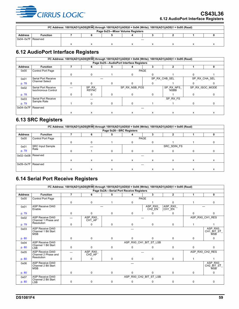
CS43L366.12 AudioPort Interface Registers
6.12 AudioPort Interface Registers
6.13 SRC Registers
6.14 Serial Port Receive Registers
0x04–0x7F Reserved —
x x x x x x x x
I2C Address: 10010(AD1)(AD0)[R/W] through 10010(AD1)(AD0)0 = 0x94 (Write); 10010(AD1)(AD0)1 = 0x95 (Read)
Page 0x25—AudioPort Interface Registers
Address Function 7 6 5 4 3 2 1 0
0x00 Control Port Page PAGE
0 0 1 0 0 1 0 1
0x01 Serial Port Receive Channel Select
— SP_RX_CHB_SEL SP_RX_CHA_SEL
p. 78 0 0 0 0 0 1 0 0
0x02 Serial Port Receive Isochronous Control
— SP_RX_RSYNC
SP_RX_NSB_POS SP_RX_NFS_NSBB
SP_RX_ISOC_MODE
p. 78 0 0 0 0 0 1 0 0
0x03 Serial Port Receive Sample Rate
— SP_RX_FS
p. 79 1 0 0 0 1 1 0 0
0x04–0x7F Reserved —
x x x x x x x x
I2C Address: 10010(AD1)(AD0)[R/W] through 10010(AD1)(AD0)0 = 0x94 (Write); 10010(AD1)(AD0)1 = 0x95 (Read)
Page 0x26—SRC Registers
Address Function 7 6 5 4 3 2 1 0
0x00 Control Port Page PAGE
0 0 1 0 0 1 1 0
0x01 SRC Input Sample Rate
— SRC_SDIN_FS
p. 79 0 1 0 0 0 0 0 0
0x02–0x08 Reserved —
x x x x x x x x
0x09–0x7F Reserved —
x x x x x x x x
I2C Address: 10010(AD1)(AD0)[R/W] through 10010(AD1)(AD0)0 = 0x94 (Write); 10010(AD1)(AD0)1 = 0x95 (Read)
Page 0x2A—Serial Port Receive Registers
Address Function 7 6 5 4 3 2 1 0
0x00 Control Port Page PAGE
0 0 1 0 1 0 1 0
0x01 ASP Receive DAI0 Enable
— ASP_RX0_CH2_EN
ASP_RX0_CH1_EN
—
p. 79 0 0 0 0 0 0 0 0
0x02 ASP Receive DAI0 Channel 1 Phase and Resolution
— ASP_RX0_CH1_AP
— ASP_RX0_CH1_RES
p. 79 0 0 0 0 0 0 1 1
0x03 ASP Receive DAI0 Channel 1 Bit Start MSB
— ASP_RX0_CH1_BIT_ST_
MSB
p. 80 0 0 0 0 0 0 0 0
0x04 ASP Receive DAI0 Channel 1 Bit Start LSB
ASP_RX0_CH1_BIT_ST_LSB
p. 80 0 0 0 0 0 0 0 0
0x05 ASP Receive DAI0 Channel 2 Phase and Resolution
— ASP_RX0_CH2_AP
— ASP_RX0_CH2_RES
p. 80 0 0 0 0 0 0 1 1
0x06 ASP Receive DAI0 Channel 2 Bit Start MSB
— ASP_RX0_CH2_BIT_ST_
MSB
p. 80 0 0 0 0 0 0 0 0
0x07 ASP Receive DAI0 Channel 2 Bit Start LSB
ASP_RX0_CH2_BIT_ST_LSB
p. 80 0 0 0 0 0 0 0 0
I2C Address: 10010(AD1)(AD0)[R/W] through 10010(AD1)(AD0)0 = 0x94 (Write); 10010(AD1)(AD0)1 = 0x95 (Read)
Page 0x23—Mixer Volume Registers
Address Function 7 6 5 4 3 2 1 0
DS1081F4 59

CS43L366.15 ID Registers
6.15 ID Registers
7 Register Descriptions
The tables in this section give bit assignments, definitions, and default states after power-up or reset. Reserved register fields must maintain default states. Section 6 describes the red, turquoise, and orange indicators.
7.1 Global Registers
0x08–0x7F Reserved —
x x x x x x x x
I2C Address: 10010(AD1)(AD0)[R/W] through 10010(AD1)(AD0)0 = 0x94(Write); 10010(AD1)(AD0)1 = 0x95 (Read)
Page 0x30—ID Registers
Address Function 7 6 5 4 3 2 1 0
0x00 Control Port Page PAGE
0 0 1 1 0 0 0 0
0x01–0x13 Reserved —
x x x x x x x x
0x14 Subrevision SUBREVISION
p. 81 x x x x x x x x
0x15 Device ID A and B (Read Only)
DEVIDA DEVIDB
p. 81 0 1 0 0 0 0 1 1
0x16 Device ID C and D (Read Only)
DEVIDC DEVIDD
p. 81 1 0 1 0 0 0 1 1
0x17 Device ID E (Read Only)
DEVIDE —
p. 81 0 1 1 0 x x x x
0x–0x7F Reserved —
x x x x x x x x
7.1.1 Revision ID Address 0x1005
R/O 7 6 5 4 3 2 1 0
AREVID MTLREVID
Default x x x x x x x x
Bits Name Description7:4 AREVID Alpha revision. CS43L36 alpha revision level. AREVID and MTLREVID form the complete device revision ID (e.g.,: A0, B2).
0x00 … 0xFF3:0 MTLREVID Metal revision. CS43L36 metal revision level. AREVID and MTLREVID form the complete device revision ID (e.g.,: A0, B2).
0x00 … 0xFF
7.1.2 Freeze Control Address 0x1006
R/W 7 6 5 4 3 2 1 0
— FREEZE
Default 0 0 0 0 0 0 0 0
Bits Name Description7:1 — Reserved0 FREEZE Freeze registers. Configures a hold on all volume-control and power-down register settings. Use this bit only during normal
operation after all circuit blocks in use have powered up. Using the bit when an affected circuit block is powering up could cause the change to occur immediately when power up completes (i.e., not gated by the FREEZE bit). Bits affected by FREEZE are shown in orange throughout Section 6 and Section 7.
0 (Default) Volume-control and power-down register changes take effect immediately.1 Modifications made to volume-control and power-down registers take effect only after this bit is cleared.
I2C Address: 10010(AD1)(AD0)[R/W] through 10010(AD1)(AD0)0 = 0x94 (Write); 10010(AD1)(AD0)1 = 0x95 (Read)
Page 0x2A—Serial Port Receive Registers
Address Function 7 6 5 4 3 2 1 0
DS1081F4 60

CS43L367.1 Global Registers
7.1.3 Serial Port SRC Control Address 0x1007
R/W 7 6 5 4 3 2 1 0
— I2C_DRIVE — SRC_BYPASS_DAC —
Default 0 0 0 1 0 0 0 0
Bits Name Description7:4 — Reserved3 I2C_
DRIVEI2C output drive strength. Selects drive strength used for the SDA output
0 (Default) Normal1 Decreased
2 — Reserved1 SRC_
BYPASS_DAC
Bypass SRC (DAC path). Determines the bypass of the input SRCs. See Section 4.6 for details. 0 (Default) No bypass1 Bypass. SRC_SDIN_FS (see p. 79) must be set equal to FsINT.
0 — Reserved
7.1.4 MCLK Status Address 0x1008
R/W 7 6 5 4 3 2 1 0
— INTERNAL_FS_STAT —
Default 0 0 0 0 0 0 x 0
Bits Name Description7:2 — Reserved1 INTERNAL_
FS_STATInternal sample rate status. Indicates the divide ratio from MCLKINT (set in INTERNAL_FS, see Section 7.1.5) to produce the internal sample rate for all converters.
0 FsINT = MCLKINT/250. Indicates that the internal MCLK is 12 or 24 MHz.1 FsINT = MCLKINT/256. Indicates that the internal MCLK is 11.2896, 12.288, 22.5792, or 24.576 MHz.
0 — Reserved
7.1.5 MCLK Control Address 0x1009
R/W 7 6 5 4 3 2 1 0
— INTERNAL_FS —
Default 0 0 0 0 0 0 1 0
Bits Name Description7:2 — Reserved1 INTERNAL_
FSInternal sample rate (FsINT). Selects the divide ratio from MCLKINT to produce the internal sample rate for all converters. See Table 4-4 for programming details. This bit always returns zero when read. Reports status in INTERNAL_FS_STAT.
0 FsINT = MCLKINT/250. Set if internal MCLK is 12 or 24 MHz.1 (Default) FsINT = MCLKINT/256. Set if internal MCLK is 11.2896, 12.288, 22.5792, or 24.576 MHz.
If MCLKINT 11.2896, 12, or 12.288 MHz, MCLKDIV must be 0. If it is 22.5792, 24, or 24.576 MHz, MCLKDIV must be 1.0 — Reserved
7.1.6 Soft Ramp Rate Address 0x100A
R/W 7 6 5 4 3 2 1 0
ASR_RATE DSR_RATE
Default 1 0 1 0 0 1 0 0
Bits Name Description7:4 ASR_
RATEAnalog soft-ramp rate (number of Fs periods between steps). Selects the soft ramp rate for all analog volumes. Step size = 1 dB or 2 dB for HPOUTx. See Section 4.2.2 for details.
0000 10001 2
0010 40011 6
0100 80101 11
0110 120111 16
1000 221001 24
1010 (Default) 331011 36
1100 441101 48
1110 661111 72
3:0 DSR_RATE
Digital soft-ramp rate (number of Fs periods between steps). Selects soft ramp rate for all digital volumes. Step size = 0.125 dB.0000 10001 2
0010 40011 6
0100 (Default) 80101 1
0110 120111 16
1000 221001 24
1010 331011 36
1100 441101 48
1110 661111 72
DS1081F4 61

CS43L367.1 Global Registers
7.1.7 Slow Start Enable Address 0x100B
R/W 7 6 5 4 3 2 1 0
— SLOW_START_EN —
Default 0 1 1 1 0 0 0 0
Bits Name Description7 — Reserved
6:4 SLOW_START_EN
Slow startup enable. Selects between fast and slow start-up times. See Section 4.2.3 for details.000 Disabled. Shortens start-up time of the volume control, DAC, and HP. Useful for high-definition audio applications. 111 (Default) Enabled
3:0 — Reserved
7.1.8 I2C Debounce Address 0x100E
R/W 7 6 5 4 3 2 1 0
I2C_SDA_DBNC_CNT I2C_SDA_DBNC_EN I2C_SCL_DBNC_CNT I2C_SCL_DBNC_EN
Default 1 0 0 0 1 0 0 0
Bits Name Description7:5 I2C_SDA_
DBNC_CNTI2C debounce count. Number of MCLKs to debounce SDA input Note: The I2C_SDA_DBNC_CNT and I2C_SCL_DBNC_CNT settings must be identical.
000 0 MCLKs001 1 MCLK
010 2 MCLKs011 3 MCLKs
100 (Default) 4 MCLKs101 5 MCLKs
110 6 MCLKs111 7 MCLKs
4 I2C_SDA_DBNC_EN
I2C SDA debounce enable. SDA debounce enableNote: The I2C_SDA_DBNC_EN and I2C_SCL_DBNC_EN settings must be identical.
0 (Default) Disabled. Must be 0 for Fast Mode or Fast-Mode Plus.1 Enabled
3:1 I2C_SCL_DBNC_CNT
I2C SCL debounce count. Number of MCLKs to debounce SCL inputNote: The I2C_SDA_DBNC_CNT and I2C_SCL_DBNC_CNT settings must be identical.
000 0 MCLKs001 1 MCLK
010 2 MCLKs011 3 MCLKs
100 (Default) 4 MCLKs101 5 MCLKs
110 6 MCLKs111 7 MCLKs
0 I2C_SCL_DBNC_EN
I2C SCL debounce count enable.Note: The settings of I2C_SDA_DBNC_EN and I2C_SCL_DBNC_EN must be identical.
0 (Default) Disabled. Must be 0 for Fast Mode or Fast-Plus Mode.1 Enabled
7.1.9 I2C Stretch Address 0x100F
R/W 7 6 5 4 3 2 1 0
I2C_STRETCH
Default 0 0 0 0 0 0 1 1
Bits Name Description7:0 I2C_
STRETCHI2C stretch. Number of additional MCLKs to clock stretch after the slave is ready
0000 0011 (Default) 3 MCLKs
7.1.10 I2C Timeout Address 0x1010
R/W 7 6 5 4 3 2 1 0
MAS_I2C_NACK MAS_TO_DIS MAS_TO_SEL ACC_TO_DIS ACC_TO_SEL
Default 1 0 1 1 0 1 1 1
Bits Name Description7 MAS_
I2C_NACK
APB master I2C NACK. Determines whether clock stretching or a NACK occurs if an APB access is attempted and I2C is not APB master.
0 I2C clock stretches if an APB access is attempted while I2C is not APB master.1 (Default) I2C NACKs if APB access is attempted while I2C is not APB master.
6 MAS_TO_DIS
APB master access timeout disable 0 (Default) Enabled 1 Disabled
5:4 MAS_TO_SEL
APB master access timeout select. Determines the timeout duration.00 64 ms 01 128 ms 10 256 ms 11 (Default) 512 ms
3 ACC_TO_DIS
APB access timeout disable.0 (Default) Enabled 1 Disabled
DS1081F4 62

CS43L367.2 Power Down and Headset Detects
7.2 Power Down and Headset Detects
2:0 ACC_TO_SEL
APB access timeout select. Determines the timeout duration in MCLKs. 000 7 MCLKs001 15 MCLKs
010 31 MCLKs011 63 MCLKs
100 127 MCLKs101 255 MCLKs
110 511 MCLKs111 (Default) 65,535 MCLKs
7.2.1 Power Down Control 1 Address 0x1101
R/W 7 6 5 4 3 2 1 0
— ASP_DAI_PDN MIXER_PDN — HP_PDN — PDN_ALL
Default 1 1 1 1 1 1 1 1
Bits Name Description
7 — Reserved
6 ASP_DAI_PDN
ASP DAI0 input path power down. Configures ASP DAI0 SDIN path power state.0 Powered up1 (Default) Powered down. Setting this bit does not tristate the serial port clock.
5 MIXER_PDN
Mixer power down. Configures the mixer power state.0 The mixer is powered up.1 (Default) The mixer is powered down.
4 — Reserved
3 HP_PDN
HPOUTx power down 0 The HP driver and DACx are powered up.1 (Default) The HP driver and DACx are powered down.
2:1 — Reserved
0 PDN_ALL
DAC power down. Configures the entire DAC’s power state except for PLL_START. After power up (PDN_ALL: 1 0), individual subblocks are powered according to power-control programming. This bit is affected by LATCH_TO_VP (see p. 75). Note: The SRC power-down state depends on the SRC_PDN_OVERRIDE setting (see p. 63).
0 Powered up, per the individual x_PDN controls1 (Default) Powered down. PDN_ALL must not be set without first enabling LATCH_TO_VP. After PDN_ALL is set and the
entire DAC is powered down, PDN_DONE is set, indicating that SCLK can be removed.
7.2.2 Power Down Control 2 Address 0x1102
R/W 7 6 5 4 3 2 1 0
— DISCHARGE_FILT+
SRC_PDN_OVERRIDE — DAC_SRC_
PDNB —
Default 1 0 0 0 0 1 0 0
Bits Name Description7:5 — Reserved4 DISCHARGE_
FILT+Discharge FILT+ capacitor. Configures the state of the FILT+ pin internal clamp. Before setting this bit, ensure that the VD_FILT device input is connected to a supply, as shown in Table 3-2.
0 (Default) FILT+ is not clamped to ground.1 FILT+ is clamped to ground. This must be set only if PDN_ALL = 1. Discharge time with an external 2.2-µF
capacitor on FILT+ is ~46 ms.3 SRC_PDN_
OVERRIDESRC power down override. Configures the SRCs’ power states.
0 (Default) Power state control for the DAC SRCs, which are controlled by the following smart logic: • DAC SRCs are off if SRC_BYPASS_DAC = 1.
• • If PDN_ALL = 1, all SRCs are off.• If PDN_ALL = 0 and the respective DAC bypass bits = 0, the following controls each SRC’s power state:
–If DAI0 is enabled, the DAC SRCs are powered up.1 DAC SRCs are controlled by DAC_SRC_PDNB.
2 — Reserved1 DAC_SRC_
PDNBDAC SRC power down. Configures the DAC ASP power state if SRC_PDN_OVERRIDE = 1.
0 (Default) Power down1 Power up audio DAC SRC only
0 — Reserved
Bits Name Description
DS1081F4 63

CS43L367.2 Power Down and Headset Detects
7.2.3 Power Down Control 3 Address 0x1103
R/W 7 6 5 4 3 2 1 0
— VPMON_PDNB —
Default 0 0 1 0 0 0 0 0
Bits Name Description7:3 — Reserved 2 VPMON_
PDNBVPMON power down. VP monitor is described in Section 4.9.1.
0 (Default) Power down VPMON.1 Power up VPMON.
1:0 — Reserved
7.2.4 Oscillator Switch Control Address 0x1107
R/W 7 6 5 4 3 2 1 0
— SCLK_PRESENT
Default 0 0 0 0 0 0 0 0
Bits Name Description7:1 — Reserved0 SCLK_
PRESENTSCLK present. Used to select the internal MCLK source. See Section 4.4 for programming details.
0→1 transition starts switch from RCO to selected internal MCLK (SCLK must be running first). 1→0 transition starts switch from selected internal MCLK to RCO (SCLK must keep running during transition).
0 (Default) SCLK may be present, but the internal MCLK is sourced from the RCO.1 SCLK is present and the internal MCLK is sourced from the SCLK pin.
7.2.5 Oscillator Switch Status Address 0x1109
R/O 7 6 5 4 3 2 1 0
— OSC_PDNB_STAT OSC_SW_SEL_STAT
Default 0 0 0 0 0 1 x x
Bits Name Description7:3 — Reserved 2 OSC_
PDNB_STATRCO power-down status. Indicates the RCO power state. See Section 4.4 for programming details.
0 RCO powered down1 (Default) RCO powered up
1:0 OSC_SW_SEL_STAT
RCO switch status. Indicates the RCO oscillator switch status. See Section 4.4 for programming details.00 In transition 01 (Default) RCO selected for internal MCLK
10–11Reserved
7.2.6 Tip Sense Control 1 Address 0x1113
R/W 7 6 5 4 3 2 1 0
TS_INV — TS_FALL_DBNCE_TIME TS_RISE_DBNCE_TIME
Default 0 0 0 1 1 0 1 1
Bits Name Description7 TS_INV Tip sense raw signal invert. Used to invert the raw signal from the tip-sense circuit. Reverses the meaning of TS_
UNPLUG_DBNC and TS_PLUG_DBNC (see p. 65).0 (Default) Not inverted 1 Inverted
6 — Reserved 5:3 TS_FALL_
DBNCE_TIMETip sense falling debounce time. Section 4.8.3 gives programming details.
000 0 ms001 125 ms
010 250 ms011 (Default) 500 ms
100 750 ms101 1.0 s
110 1.25 s111 1.5 s
2:0 TS_RISE_DBNCE_TIME
Tip sense rising debounce time. Section 4.8.3 gives programming details.000 0 ms001 125 ms
010 250 ms011 (Default) 500 ms
100 750 ms101 1.0 s
110 1.25 s111 1.5 s
DS1081F4 64

CS43L367.3 Clocking Registers
7.3 Clocking Registers
7.2.7 Tip Sense Indicator Status Address 0x1115
R/O 7 6 5 4 3 2 1 0
— TS_UNPLUG_DBNC
TS_PLUG_DBNC —
Default 0 0 0 0 x x x x
Bits Name Description7:4 — Reserved3 TS_
UNPLUG_DBNC
Tip sense unplug debounce status. See Section 4.8.3 for details. Setting TS_INV reverses the meaning of this bit. 0 Condition is not present.1 Condition is present.
2 TS_PLUG_DBNC
Tip sense plug debounce status. See Section 4.8.3 for details. Setting TS_INV reverses the meaning of this bit.0 Condition is not present.1 Condition is present.
1:0 — Reserved
7.3.1 MCLK Source Select Address 0x1201
R/W 7 6 5 4 3 2 1 0
— MCLKDIV MCLK_SRC_SEL
Default 0 0 0 0 0 0 0 0
Bits Name Description7:2 — Reserved1 MCLKDIV Master clock divide ratio. Selects the divide ratio between the selected MCLK source and the MCLKINT. Section 4.4.2 lists
supported MCLK rates and their associated programming settings. 0 (Default) Divide by 1 (source MCLKINT = ~12 MHz). 1 Divide by 2 (source MCLKINT = ~24 MHz)
Note: Change this field only if PDN_ALL = 1.0 MCLK_
SRC_SEL
Master clock source select. Selects the internal master clock source. For programming details and examples, see Section 4.4. 0 (Default) SCLK pin1 PLL clock
7.3.2 FSYNC Pulse Width, Lower Byte Address 0x1203
R/W 7 6 5 4 3 2 1 0
FSYNC_PULSE_WIDTH_LB
Default 0 0 0 0 0 0 0 0
Bits Name Description7:0 FSYNC_
PULSE_WIDTH_
LB
FSYNC pulse width LB. FSYNC_PULSE_WIDTH_UB | FSYNC_PULSE_WIDTH_LB provides an 11-bit field to set the duty cycle of LRCK in Hybrid-Master Mode. These combined value forms an integer number of SCLK periods within an LRCK frame that governs the LRCK high time. See Section 4.5.2 for usage details and Section 5 for a programming example. The value must be 1 less than the desired width of the LRCK pulse, measured in SCLK counts, as illustrated by the value below.FSYNC_PULSE_WIDTH_UB | FSYNC_PULSE_WIDTH_LB yield the following setting value:
000 0000 0000 (Default) LRCK is one SCLK wide.
7.3.3 FSYNC Pulse Width, Upper Byte Address 0x1204
R/W 7 6 5 4 3 2 1 0
— FSYNC_PULSE_WIDTH_UB
Default 0 0 0 0 0 0 0 0
Bits Name Description7:3 — Reserved2:0 FSYNC_PULSE_
WIDTH_UBFSYNC pulse width UB. See description for FSYNC_PULSE_WIDTH_LB in Section 7.3.2.
000 (Default)
DS1081F4 65

CS43L367.3 Clocking Registers
7.3.4 FSYNC Period, Lower Byte Address 0x1205
R/W 7 6 5 4 3 2 1 0
FSYNC_PERIOD_LB
Default 1 1 1 1 1 0 0 1
Bits Name Description7:0 FSYNC_
PERIOD_LB
FSYNC period LB. FSYNC_PERIOD_UB | FSYNC_PERIOD_LB controls frequency (number of SCLKs per LRCK) of LRCK for ASP. Section 4.5.2 for details on how this register is used and Section 5 for a programming example. The final SCLKs per LRCK count is +1 of the value set in the UB|LB register fieldFSYNC_PERIOD_UB | FSYNC_PERIOD_LB yield the following setting values:
0x000 1 SCLK/LRCK … 0x0F9 (Default) 250 SCLKs/ LRCK … 0xFFF 4096 SCLKs/ LRCK
7.3.5 FSYNC Period, Upper Byte Address 0x1206
R/W 7 6 5 4 3 2 1 0
— FSYNC_PERIOD_UB
Default 0 0 0 0 0 0 0 0
Bits Name Description7:4 — Reserved3:0 FSYNC_
PERIOD_UBFSYNC period UB. See description for FSYNC_PERIOD_LB in Section 7.3.4.
0000 (Default)
7.3.6 ASP Clock Configuration 1 Address 0x1207
R/W 7 6 5 4 3 2 1 0
— ASP_SCLK_EN ASP_HYBRID_MODE — ASP_SCPOL_IN_DAC ASP_LCPOL_OUT ASP_LCPOL_IN
Default 0 0 0 0 0 0 0 0
Bits Name Description7:6 — Reserved5 ASP_SCLK_
ENASP SCLK enable. Must be set if DAI functionality is used.
0 (Default) Disabled 1 Enabled
4 ASP_HYBRID_
MODE
ASP Hybrid-Master Mode. Allows the internal LRCK to be generated from SCLK. See Fig. 4-15 for details.0 (Default) LRCK is input from external source which is synchronous to SCLK (Slave Mode).1 LRCK is an output generated from SCLK (Hybrid Master Mode).
3 — Reserved2 ASP_SCPOL_
IN_DACASP SCLK input polarity. Determines the polarity for the DAC path. See Fig. 4-15 for details.
0 (Default) SDIN latched on falling edge1 SDIN latched on rising edge
1 ASP_LCPOL_OUT
ASP LRCK output drive polarity. Determines the polarity for the ASP LRCK output drive. See Fig. 4-15 for details.0 (Default) Normal1 Inverted
0 ASP_LCPOL_IN
ASP LRCK input polarity. Determines ASP LRCK input polarity (pad to logic). See Fig. 4-15 for details.0 (Default) Normal1 Inverted
DS1081F4 66

CS43L367.3 Clocking Registers
7.3.7 ASP Frame Configuration Address 0x1208
R/W 7 6 5 4 3 2 1 0
— ASP_STP ASP_5050 ASP_FSD
Default 0 0 0 1 0 0 0 0
Bits Name Description7:5 — Reserved4 ASP_
STPASP start phase. Controls which LRCK/FSYNC phase starts a frame. See Section 4.5.5 for details.
0 The frame begins when LRCK/FSYNC transitions from high to low1 (Default) The frame begins when LRCK/FSYNC transitions from low to high
3 ASP_5050
ASP LRCK fixed 50/50 duty cycle. Determines whether the duty cycle is fixed or programmable. See Section 4.5.5 for details.0 (Default) Programmable duty cycle. Determined by FSYNC_PULSE_WIDTH_LB (see p. 65), FSYNC_PULSE_WIDTH_
UB, and FSYNC_PERIOD_xSB (see p. 66).1 50/50 Mode. Fixed 50% duty cycle
2:0 ASP_FSD
ASP frame-start delay. Determines the delay before the start of an ASP frame in ASP_SCLK periods. See Section 4.5.2.000 (Default) 0 delay 001 0.5 delay 010 1.0 delay … 101 2.5 delay 110–111 Reserved
7.3.8 FS Rate Enable Address 0x1209
R/W 7 6 5 4 3 2 1 0
— FS_EN
Default 0 0 0 0 0 0 0 0
Bits Name Description7:3 — Reserved2:0 FS_EN Fs rate enable. Provides enables for all internally generated Fs rates. 0 = disabled; 1 = enabled. Section 4.6 gives details.
FS_EN[0] Enable IASRC 96K and lower rates.FS_EN[2] Enable IASRC 192, 176.4, and 176.471 K rates00 (Default) All disabled
7.3.9 Input ASRC Clock Select Address 0x120A
R/W 7 6 5 4 3 2 1 0
— CLK_IASRC_SEL
Default 0 0 0 0 0 0 0 0
Bits Name Description7:2 — Reserved1:0 CLK_IASRC_
SELInput ASRC clock select. Selects input ASRC MCLKINT frequency. See Section 4.6 for programming details.
00 (Default) 6 MHz 01 12 MHz 10 24 MHz 11 Reserved
7.3.10 PLL Divide Configuration 1 Address 0x120C
R/W 7 6 5 4 3 2 1 0
— PLL_REF_INV SCLK_PREDIV
Default 0 0 0 0 0 0 0 0
Bits Name Description7:3 — Reserved2 PLL_REF_
INVInvert PLL reference clock. See Table 4.4.3 for programming guidelines.
0 (Default) Normal1 Inverted
1:0 SCLK_PREDIV
PLL reference divide select. See Table 4.4.3 for programming guidelines.00 (Default) Divide by 1 01 Divide by 2 10 Divide by 4 11 Divide by 8
DS1081F4 67

CS43L367.4 Interrupt Registers
7.4 Interrupt Registers
7.4.1 Channel Overflow Interrupt Status Address 0x1302
R/O 7 6 5 4 3 2 1 0
— CHA_OVFL CHB_OVFL
Default 0 0 0 0 x x x x
Bits Name Description7:2 — Reserved1 CHA_
OVFLChannel overflow. Indicates the overrange status in the corresponding signal path. Rising-edge state transitions may cause an interrupt, depending on the programming of the associated interrupt mask bit.
0 No digital clipping has occurred in the data path of the respective signal source.1 Digital clipping has occurred in the data path of the respective signal source.
0 CHB_OVFL
7.4.2 SRC Interrupt Status Address 0x1303
R/O 7 6 5 4 3 2 1 0
— SRC_IUNLK — SRC_ILK
Default 0 0 0 0 x x x x
Bits Name Description7:3 — Reserved2 SRC_IUNLK SRC unlock status. Indicates SRC unlock status for the input path. Status is valid only if serial-port LRCK is toggling.
0 Locked1 Unlocked
1 — Reserved0 SRC_ILK SRC lock status. Indicates SRC lock status for the ASP input path. Status is valid only if serial-port LRCK is toggling.
0 Unlocked1 Locked
7.4.3 ASP RX Interrupt Status Address 0x1304
R/O 7 6 5 4 3 2 1 0
— ASPRX_OVLD ASPRX_ERROR ASPRX_LATE ASPRX_EARLY ASPRX_NOLRCK
Default 0 0 0 x x x x x
Bits Name Description7:5 — Reserved4 ASPRX_
OVLDASP RX request overload. Set when too many input buffers request processing at once. 0No interrupt1 Interrupt detected. ASP RX cannot retrieve data from the internal input buffers because at least one of the following
violations has occurred: —The ASP RX core clock frequency is less than SCLK/8. —The LRCK frame (non-50/50 Mode) or LRCK subframe (50/50 Mode) period is less than 16 SCLK periods (assuming
the ASP RX core clock frequency is equal to SCLK/8).3 ASPRX_
ERRORASP RX LRCK error. Logical OR of ASPRX_LATE and ASPRX_EARLY, described below.
0 No interrupt1 Interrupt detected
2 ASPRX_LATE
ASP RX LRCK late. Determines whether the number of SCLK periods per LRCK phase (high or low) is greater than the expected count, as determined by the FSYNC_PERIOD_xSB and FSYNC_PULSE_WIDTH_x fields.
0 No interrupt1 Interrupt detected
1 ASPRX_EARLY
ASP RX LRCK early. Determines whether the number of SCLK periods per LRCK phase (high or low) is less than the expected count, as determined by FSYNC_PERIOD_xSB (see p. 66) and FSYNC_PULSE_WIDTH_x (see p. 65).
0 No interrupt1 Interrupt detected
0 ASPRX_NOLRCK
ASP RX no LRCK. Determines whether the SCLK periods counted exceeds twice the value of LRCK period (FSYNC_PERIOD_xSB) without an LRCK edge.
0 No interrupt1 Interrupt detected
DS1081F4 68

CS43L367.4 Interrupt Registers
n,
7.4.4 DAC Interrupt Status Address 0x1308
R/O 7 6 5 4 3 2 1 0
— PDN_DONE
Default 0 0 0 0 0 0 0 x
Bits Name Description7:1 — Reserved0 PDN_
DONEPower-down done. Indicates when the DAC has powered down and MCLK can be stopped, as determined by various power-control and headset-interface register settings.
0 Not completely powered down1 Powered down as a result of PDN_ALL having been set.
7.4.5 Detect Interrupt Status 1 Address 0x1309
R/O 7 6 5 4 3 2 1 0
— TIP_SENSE_PLUG TIP_SENSE_UNPLUG —
Default x x x x x x x x
Bits Name Description7 — Reserved6 TIP_SENSE_PLUG Tip sense plug event. Indicates the undebounced status of a plug event on the TIP_SENSE pin.1
0 No HP plug event1 HP plug event
1. It is active only if TIP_SENSE_CTRL (p. 75) is configured so the tip-sense circuit is powered up. If the system is configured for standby operatiothe sticky version of this bit (that also accounts for events that occurred during standby) can be read back after a wake event.
5 TIP_SENSE_UNPLUG Tip sense unplug event. Indicates the undebounced status of an unplug event on the TIP_SENSE pin.1 0 (Default) No HP unplug event1 HP unplug event
4:0 — Reserved
7.4.6 SRC Partial Lock Interrupt Status Address 0x130B
R/O 7 6 5 4 3 2 1 0
— DAC_UNLK — DAC_LK —
Default x x x x x x x x
Bits Name Description7 — Reserved6 DAC_UNLK ASP input SRC unlock status.
0 Locked1 Unlocked
5:3 — Reserved2 DAC_LK ASP input partial SRC lock status.
0 Unlocked1 Locked
1:0 — Reserved
7.4.7 VP Monitor Interrupt Status Address 0x130D
R/O 7 6 5 4 3 2 1 0
— VPMON_TRIP
Default 0 0 0 0 0 0 0 x
Bits Name Description7:1 — Reserved0 VPMON_TRIP VP monitor interrupt. If the VP power supply falls below 2.6 V, this bit is set. See Section 4.9.1 for details.
0 No interrupt1 Interrupt detected
DS1081F4 69

CS43L367.4 Interrupt Registers
7.4.8 PLL Lock Interrupt Status Address 0x130E
R/O 7 6 5 4 3 2 1 0
— PLL_LOCK
Default 0 0 0 0 0 0 0 x
Bits Name Description7:1 — Reserved0 PLL_LOCK PLL lock. Indicates the lock state of the PLL.
0 No interrupt1 Interrupt detected
7.4.9 Tip Sense Plug/Unplug Interrupt Status Address 0x130F
R/O 7 6 5 4 3 2 1 0
— TS_UNPLUG TS_PLUG –
Default 0 0 0 0 x x x x
Bits Name Description7:4 — Reserved3 TS_UNPLUG Tip sense unplug status. See Section 4.8.3 for details. Setting TS_INV reverses the meaning of this bit.
0 Condition is not present.1 Condition is present.
2 TS_PLUG Tip sense plug status. See Section 4.8.3 for details. Setting TS_INV reverses the meaning of this bit.0 Condition is not present.1 Condition is present.
1:0 — Reserved
7.4.10 Mixer Interrupt Mask Address 0x1317
R/W 7 6 5 4 3 2 1 0
— M_CHA_OVFL M_CHB_OVFL
Default 0 0 0 0 1 1 1 1
Bits Name Description7:2 — Reserved1 M_CHA_OVFL CHx_OVFL mask.
0 Unmasked1 (Default) Masked
0 M_CHB_OVFL
7.4.11 SRC Interrupt Mask Address 0x1318
R/W 7 6 5 4 3 2 1 0
— M_SRC_IUNLK — M_SRC_ILK
Default 0 0 0 0 1 1 1 1
Bits Name Description7:3 — Reserved2 M_SRC_
IUNLKSRC_IUNLK mask.
0 Unmasked1 (Default) Masked
1 — Reserved0 M_SRC_ILK SRC_ILK mask.
0 Unmasked1 (Default) Masked
DS1081F4 70

CS43L367.4 Interrupt Registers
7.4.12 ASP RX Interrupt Mask Address 0x1319
R/W 7 6 5 4 3 2 1 0
— M_ASPRX_OVLD M_ASPRX_ERROR M_ASPRX_LATE M_ASPRX_EARLY M_ASPRX_NOLRCK
Default 0 0 0 1 1 1 1 1
Bits Name Description7:5 — Reserved4 M_ASPRX_
OVLDASPRX_OVFL mask.
0 Unmasked1 (Default) Masked
3 M_ASPRX_ERROR
ASPRX_ERROR mask.0 Unmasked1 (Default) Masked
2 M_ASPRX_LATE
ASPRX_LATE mask.0 Unmasked1 (Default) Masked
1 M_ASPRX_EARLY
ASPRX_EARLY mask.0 Unmasked1 (Default) Masked
0 M_ASPRX_NOLRCK
ASPRX_NOLRCK mask.0 Unmasked1 (Default) Masked
7.4.13 DAC Interrupt Mask Address 0x131B
R/W 7 6 5 4 3 2 1 0
— M_PDN_DONE
Default 0 0 0 0 0 0 1 1
Bits Name Description7:1 — Reserved0 M_PDN_
DONEPDN_DONE mask.
0 Unmasked1 (Default) Masked
7.4.14 SRC Partial Lock Interrupt Mask Address 0x131C
R/W 7 6 5 4 3 2 1 0
— M_DAC_UNLK — M_DAC_LK —
Default 0 1 1 1 1 1 1 1
Bits Name Description7 — Reserved6 M_DAC_
UNLKASP input unlock mask.
0 Unmasked1 (Default) Masked
5–3 — Reserved2 M_DAC_LK ASP input lock mask.
0 Unmasked1 (Default) Masked
1:0 — Reserved
DS1081F4 71

CS43L367.5 Fractional-N PLL Registers
7.5 Fractional-N PLL Registers
7.4.15 VP Monitor Interrupt Mask Address 0x131E
R/W 7 6 5 4 3 2 1 0
— M_VPMON_TRIP
Default 0 0 0 0 0 0 0 1
Bits Name Description7:1 — Reserved0 M_
VPMON_TRIP
VP monitor mask. 0 Unmasked. Unmask/enable this bit only when VP exceeds the detection voltage threshold; applicable to power-up
conditions or if VP is not at its steady-state voltage.1 (Default) Masked
7.4.16 PLL Lock Mask Address 0x131F
R/W 7 6 5 4 3 2 1 0
— M_PLL_LOCK
Default 0 0 0 0 0 0 0 1
Bits Name Description7:1 — Reserved0 M_PLL_
LOCKPLL lock mask.
0 Unmasked1 (Default) Masked
7.4.17 Tip Sense Plug/Unplug Interrupt Mask Address 0x1320
R/W 7 6 5 4 3 2 1 0
— M_TS_UNPLUG M_TS_PLUG —
Default 0 0 0 0 1 1 1 1
Bits Name Description7:4 — Reserved3 M_TS_
UNPLUGTip sense unplug mask.
0 Unmasked1 (Default) Masked
2 M_TS_PLUG
Tip sense plug mask.0 Unmasked1 (Default) Masked
1:0 — Reserved
7.5.1 PLL Control 1 Address 0x1501
R/W 7 6 5 4 3 2 1 0
— PLL_START
Default 0 0 0 0 0 0 0 0
Bits Name Description7:1 — Reserved0 PLL_
STARTPLL start. If MCLK_SRC_SEL = 0, the PLL is bypassed and can be powered down by clearing PLL_START. See Section 4.4.3.
0 (Default) Powered off. 1 Powered on
DS1081F4 72

CS43L367.5 Fractional-N PLL Registers
7.5.2 PLL Division Fractional Bytes 0–2 Address 0x1502–0x1504
R/W 7 6 5 4 3 2 1 0
0x1502 PLL_DIV_FRAC[7:0]
0x1503 PLL_DIV_FRAC[15:8]
0x1504 PLL_DIV_FRAC[23:16]
Default 0 0 0 0 0 0 0 0
Bits Name Description7:0 PLL_DIV_
FRAC[7:0]PLL fractional portion of divide ratio LSB. See Section 4.4.3 for details. There are 3 bytes of PLL feedback divider fraction portion: This is LSB byte; e.g., 0xFF means (2–17 + 2–18 + …+2–24)
0000 0000 (Default)7:0 PLL_DIV_
FRAC[15:8]PLL fractional portion of divide ratio middle byte; e.g., 0xFF means (2–9 + 2–10 + …+2–16). See Section 4.4.3 for details.
0000 0000 (Default)7:0 PLL_DIV_
FRAC[23:16]PLL fractional portion of divide ratio MSB; e.g., 0xFF means (2–1 + 2–2 + …+2–8). See Section 4.4.3 for details.
0000 0000 (Default)
7.5.3 PLL Division Integer Address 0x1505
R/W 7 6 5 4 3 2 1 0
PLL_DIV_INT
Default 0 1 0 0 0 0 0 0
Bits Name Description7:0 PLL_DIV_INT PLL integer portion of divide ratio. Integer portion of PLL feedback divider. See Section 4.4.3 for details.
0100 0000 (Default)
7.5.4 PLL Control 3 Address 0x1508
R/W 7 6 5 4 3 2 1 0
PLL_DIVOUT
Default 0 0 0 1 0 0 0 0
Bits Name Description7:0 PLL_
DIVOUTFinal PLL clock output divide value. See Section 4.4.3 for configuration details.
0001 0000 (Default)
7.5.5 PLL Calibration Ratio Address 0x150A
R/W 7 6 5 4 3 2 1 0
PLL_CAL_RATIO
Default 1 0 0 0 0 0 0 0
Bits Name Description7:0 PLL_CAL_
RATIO PLL calibration ratio. See Section 4.4.3 for configuration details. Target value for PLL VCO calibration.
1000 0000 (Default)
7.5.6 PLL Control 4 Address 0x151B
R/W 7 6 5 4 3 2 1 0
— PLL_MODE
Default 0 0 0 0 0 0 1 1
Bits Name Description7:2 — Reserved 1:0 PLL_
MODEPLL bypass mode. Configures 500/512 and 1029/1024 factor bypasses. See Section 4.4.3 for configuration details.
00 Unsupported01 500/512 only (1029/1024 bypassed)
10 1029/1024 only (500/512 bypassed)11 (Default) Both bypassed
DS1081F4 73

CS43L367.6 HP Load-Detect Registers
7.6 HP Load-Detect Registers
7.7 Headset Interface Registers
7.6.1 Load-Detect R/C Status Address 0x1925
R/O 7 6 5 4 3 2 1 0
— CLA_STAT — RLA_STAT
Default 0 0 0 0 0 0 0 0
Bits Name Description7:6 — Reserved4 CLA_STAT Capacitor load-detection result for HPA. See Section 4.2.2 for details.
Note: Low capacitance results were determined with CL = 1 nF; high capacitance results were determined with CL = 10 nF.0 (Default) High capacitance (CL ~2 nF)1 Low capacitance (CL < ~2 nF)
1:0 RLA_STAT Resistor load-detection result for HPA. See Section 4.2.2 for details. 00 (Default) 15 01 30
10 3 k11 Reserved
7.6.2 HP Load Detect Done Address 0x1926
R/O 7 6 5 4 3 2 1 0
— HPLOAD_DET_DONE
Default 0 0 0 0 0 0 0 0
Bits Name Description7:1 — Reserved0 HPLOAD_
DET_DONEHP load detect done. Indicates whether HP load detection is finished. See Section 4.2.2 for details.
0 (Default) HP load is not finished.1 HP load is finished.
7.6.3 HP Load Detect Enable Address 0x1927
R/O 7 6 5 4 3 2 1 0
— HP_LD_EN
Default 0 0 0 0 0 0 0 0
Bits Name Description7:1 — Reserved0 HP_LD_EN HP load detect enable. A 0-to-1 bit transition initiates load detection. See Section 4.2.2 for details.
0 (Default) Disabled1 Enabled
7.7.1 Wake Control Address 0x1B71
R/W 7 6 5 4 3 2 1 0
— M_HP_WAKE WAKEB_MODE — WAKEB_CLEAR
Default 1 1 0 0 0 0 0 0
Bits Name Description7 — Reserved6 M_HP_
WAKEMask tip sense wake.1 Configures the mask for the tip-sense wake status.
0 Unmasked. The occurrence of a wake interrupt affects WAKE. Before unmasking, pending wake events must be cleared via WAKEB_CLEAR.
1 (Default) Masked. The occurrence of a wake interrupt does not affect WAKE. 5 WAKEB_
MODEWAKE output mode.1 Configures the mode of operation for the WAKE output
0 (Default) Output is latched low after a trigger event until WAKEB_CLEAR is toggled.1 Output follows the combination logic directly (nonlatched).
4:1 — Reserved
DS1081F4 74

CS43L367.7 Headset Interface Registers
0 WAKEB_CLEAR
WAKE output clear. Applicable only if WAKEB_MODE = 0 and an event triggers the WAKE output to latch low.0 (Default) WAKE output normal operation. If WAKEB_MODE = 1, WAKEB_CLEAR does not deassert WAKE, but clears
TIP_SENSE_PLUG, TIP_SENSE_UNPLUG in the VP domain.1 WAKE output deasserted (the TIP_SENSE_PLUG, TIP_SENSE_UNPLUG bits in the VP domain are also cleared).
1.This bit can be changed only if LATCH_TO_VP is enabled (see p. 75).
7.7.2 Tip Sense Control 2 Address 0x1B73
R/W 7 6 5 4 3 2 1 0
TIP_SENSE_CTRL TIP_SENSE_INV — TIP_SENSE_DEBOUNCE
Default 0 0 0 0 0 0 1 0
Bits Name Description7:6 TIP_SENSE_
CTRLTip sense control.Configures operation of the tip-sense circuit. Note: This bit can be updated only if LATCH_TO_VP (see p. 75) is enabled.
00 (Default) Disabled. The tip-sense circuit is powered down and does not report to the status registers (TIP_SENSE_PLUG and TIP_SENSE_UNPLUG in the VP domain are also cleared).
01 Digital input. Internal weak current source pull-up is disabled.10 Reserved11 Short detect. Internal weak current source pull-up is enabled.
5 TIP_SENSE_INV
Tip sense invert. Used to invert the signal from the tip-sense circuit. Updatable only if LATCH_TO_VP is enabled.
0 (Default) Not inverted 1 Inverted
4:2 — Reserved1:0 TIP_SENSE_
DEBOUNCETip sense debounce time. Sets tip sense unplug event (TIP_SENSE = 0) debounce time before status is reported. Timings are approximate and vary with MCLKINT and FsINT.
00 No debounce 01 200 ms 10 (Default) 500 ms 11 1000 ms
7.7.3 Mic Detect Control 1 Address 0x1B75
R/W 7 6 5 4 3 2 1 0
LATCH_TO_VP EVENT_STATUS_SEL —
Default 0 0 0 1 1 1 1 1
Bits Name Description7 LATCH_
TO_VPLatch to VP registers. Controls the transfer of writable control registers in the VD_FILT supply domain to duplicate registers in the VP supply domain. Can be used to enable setting sticky status bits in the VP domain.
0 (Default) Inhibits the transfer of VD_FILT registers to VP registers (latched mode). Enables the setting of VP sticky status latches.
1 Transfers VD_FILT fields to VP fields (transparent mode). Disables setting of VP sticky status latches.Affected registers: • TIP_SENSE_CTRL on p. 75 • TIP_SENSE_INV on p. 75
• M_HP_WAKE on p. 74 • WAKEB_MODE p. 74
Note: The description of PDN_ALL on p. 63 describes the interdependency between LATCH_TO_VP and PDN_ALL. 6 EVENT_
STATUS_SEL
Event status selection. Selects the level of processing on readable status originating in the VP supply domain. 0 (Default) Raw (unprocessed) status events are selected.1 Sticky processed status events are selected.
Affected registers: • TIP_SENSE_PLUG on p. 69 • TIP_SENSE_UNPLUG on p. 69
•
5:0 — Reserved
Bits Name Description
DS1081F4 75

CS43L367.8 DAC Control Registers
7.8 DAC Control Registers
7.7.4 Detect Status 1 Address 0x1B77
R/O 7 6 5 4 3 2 1 0
TIP_SENSE —
Default x x 0 x x x x x
Bits Name Description7 TIP_SENSE TIP_SENSE circuit status. The plug-to-unplug edge is debounced for the set debounce time (see TIP_SENSE_
DEBOUNCE, p. 75). 0 HP not plugged in1 HP plugged in
6:0 — Reserved
7.7.5 Detect Interrupt Mask 1 Address 0x1B79
R/W 7 6 5 4 3 2 1 0
— M_TIP_SENSE_PLUG M_TIP_SENSE_UNPLUG —
Default 1 1 1 0 0 0 0 0
Interrupt mask register bits serve as a mask for the interrupt sources in the interrupt status registers. Interrupts are described in Section 4.12.
Bits Name Description7 — Reserved6 M_TIP_
SENSE_PLUG
TIP_SENSE_PLUG mask0 Unmasked1 (Default) Masked
5 M_TIP_SENSE_UNPLUG
TIP_SENSE_UNPLUG mask0 Unmasked1 (Default) Masked
4:0 — Reserved
7.8.1 DAC Control 1 Address 0x1F01
R/W 7 6 5 4 3 2 1 0
— DACB_INV DACA_INV
Default 0 0 0 0 0 0 0 0
Bits Name Description7:2 — Reserved1:0 DACx_INV DACx invert signal polarity. Configures the polarity of the DAC channel x signal. See Section 4.2 for details.
0 (Default) Not inverted1 Inverted
7.8.2 DAC Control 2 Address 0x1F06
R/W 7 6 5 4 3 2 1 0
HPOUT_PULLDOWN HPOUT_LOAD HPOUT_CLAMP DAC_HPF_EN —
Default 0 0 0 0 0 0 1 0
Bits Name Description7:4 HPOUT_
PULLDOWNAlthough bits 2:0 are independent, the final resistance from the resistor string is dictated by the lowest resistance chosen; e.g., if HPOUT_PULLDOWN = 1011, a nominal 6-k pull-down resistance results even if 9.6-k resistance is also selected.
0000 (Default) 0.9 k0001–0111 0.9 k
1000 No pulldown1001 9.3 k
1010 5.8 k1011 Reserved
1100 0.9 k1101–1111 Reserved
3 HPOUT_LOAD
HP output load. Sets HP amplifier capacitive load capability. Table 3-7 gives output specifications. See Section 4.2 for details.
0 (Default) 1 nF Mode1 10 nF Mode
Note: The HP path must be powered down before reconfiguring this bit and repowered afterwards. See Section 4.2.2.
DS1081F4 76

CS43L367.9 HP Control Register
7.9 HP Control Register
7.10 Class H Register
7.11 Volume Control
2 HPOUT_CLAMP
HPOUT clamp. Configures an override of the HPOUT clamp to ground when the channels are powered down.0 (Default) Clamp to ground when channels are powered down.1 Clamp is disabled when the channels are powered down. The pulldown to GNDA depends on the HPOUT_
PULLDOWN setting.1 DAC_HPF_
ENDAC high-pass filter enable. Configures the internal HPF before DAC. Changes to this bit must be made only if PDN_ALL = 1. See Section 4.2 for details.
0 Disabled. This must be cleared only for test purposes.1 (Default) Enabled. The corner frequency is set to 0.935 Hz when FsINT = 48 kHz.
0 — Reserved
7.9.1 HP Control Address 0x2001
R/W 7 6 5 4 3 2 1 0
— ANA_MUTE_B ANA_MUTE_A FULL_SCALE_VOL —
Default 0 0 0 0 1 1 0 1
Bits Name Description7:4 — Reserved3 ANA_MUTE_
BAnalog mute Channel B. See Section 4.2 for details.
0 Unmuted1 (Default) Muted
2 ANA_MUTE_A
Analog mute Channel A. See Section 4.2 for details.0 Unmuted1 (Default) Muted
1 FULL_SCALE_VOL
Full-scale volume. Determines the maximum volume for the headphone output. See Section 4.2 for details.0 (Default) 0 dB 1 –6 dB. This setting is recommended if the load is approximately 15 .
0 — Reserved
7.10.1 Class H Control Address 0x2101
R/W 7 6 5 4 3 2 1 0
— ADPTPWR
Default 0 0 0 0 0 1 1 1
Bits Name Description7:3 — Reserved2:0 ADPTPWR Adaptive power adjustment. Configures how power to HP output amplifiers adapts to the output signal level. Section 4.2
gives detailed descriptions of supported settings. 000 Reserved001 Fixed, Mode 0—VP_CP Mode (±2.5V)010 Fixed, Mode 1—VCP Mode (±VCP)011 Fixed, Mode 2 —VCP/2 Mode (±VCP/2)
100 Fixed, Mode 3 —VCP/3 Mode (±VCP/3)101–110 Reserved111 (Default) Adapt to signal. The output signal dynamically determines
the voltage level.
7.11.1 Channel A Input Volume Address 0x2301
R/W 7 6 5 4 3 2 1 0
— CHA_VOL
Default 0 0 1 1 1 1 1 1
Bits Name Description7:6 — Reserved5:0 CHA_
VOLInput attenuation. Sets the attenuation level to be applied to various stereo digital inputs. See Section 4.1 for details. Each input can be muted or attenuated from –62 to 0 dB in 1-dB steps.
00 0000 0 dB00 0001 –1.0 dB …
11 1110 –62.0 dB11 1111 (Default) Mute.
Bits Name Description
DS1081F4 77

CS43L367.12 AudioPort Interface Registers
7.12 AudioPort Interface Registers
7.11.2 Channel B Input Volume Address 0x2303
R/W 7 6 5 4 3 2 1 0
— CHB_VOL
Default 0 0 1 1 1 1 1 1
Bits Name Description7:6 — Reserved5:0 CHB_
VOLInput attenuation. Sets the attenuation level to be applied to various stereo digital inputs. See Section 4.1 for details. Each input can be muted or attenuated from –62 to 0 dB in 1-dB steps.
00 0000 0 dB00 0001 –1.0 dB …
11 1110 –62.0 dB11 1111 (Default) Mute.
7.12.1 Serial Port Receive Channel Select Address 0x2501
R/W 7 6 5 4 3 2 1 0
— SP_RX_CHB_SEL SP_RX_CHA_SEL
Default 0 0 0 0 0 1 0 0
Bits Name Description7:4 — Reserved3:2 SP_RX_
CHB_SELSP RX Channel B select for DAI0. Selects right input channel. See Section 5 for programming examples.
00 Channel 0 01 (Default) Channel 1 10 Channel 2 11 Channel 3 1:0 SP_RX_
CHA_SELSP RX Channel A select for DAI0. Selects right input channel.
00 (Default) Channel 0 01 Channel 1 10 Channel 2 11 Channel 3
7.12.2 Serial Port Receive Isochronous Control Address 0x2502
R/W 7 6 5 4 3 2 1 0
— SP_RX_RSYNC SP_RX_NSB_POS SP_RX_NFS_NSBB SP_RX_ISOC_MODE
Default 0 0 0 0 0 1 0 0
Bits Name Description7 — Reserved6 SP_RX_
RSYNCSerial port receive synchronization.
0 (Default) Normal state1 Recenter the FIFO. No read and writes when asserted
5:3 SP_RX_NSB_POS
Serial-port receive null-sample bit position. Selects the position of the null byte in the resultant 16-, 24-, or 32-bit sample.For all samples, if SP_RX_ISOC_MODE ≠ 00, SP_RX_NFS_NSBB = 0, the following applies: • For a 16-bit sample (8-bit audio + null byte), [23:16] is the null byte. • For a 24-bit sample (16-bit audio + null byte), [15:8] is the null byte. • For a 32-bit sample (24-bit audio + null byte), [7:0] is the null byte. Note: NSB Mode does not support 32-bit audio samples.The ASP_RXn_CHn_RES fields in Section 7.14 set the output resolution of the ASP receive channel samples.Clearing SP_RX_NSB_POS indicates that Bit 0 must be zero for the sample to be classified as a null.
000 (Default) 0 … 111 72 SP_RX_
NFS_NSBB
Serial-port receive NSB/NFS Mode select.0 NSB Mode valid only if SP_RX_ISOC_MODE ≠ 00. 1 (Default) NFS Mode
1:0 SP_RX_ISOC_MODE
Serial port receive isochronous mode. Selecting an isochronous mode allows for null removal. The ASP Rx rate bits (SP_RX_FS, see p. 79) are used only to help the device determine when to insert nulls.
00 (Default) Native mode 01 48k isochronous stream
10 96k isochronous stream 11 192k isochronous stream
DS1081F4 78

CS43L367.13 SRC Registers
7.13 SRC Registers
7.14 Serial Port Receive Registers
7.12.3 Serial Port Receive Sample Rate Address 0x2503
R/W 7 6 5 4 3 2 1 0
— SP_RX_FS
Default 1 0 0 0 1 1 0 0
Bits Name Description7:5 — Reserved4:0 SP_
RX_FS
SP receive sample rate. Configures the sample rate of the SRC FSI when in Isochronous Mode. This setting autoscales when configuring for a isochronous rate of 96 or 192 kHz with respect to the 48-kHz isochronous rate, e.g., 24-kHz setting in isochronous rate of 48 kHz would be scaled to a 48-kHz setting in isochronous rate of 96 kHz.
0 0000 Reserved0 0001 8.00 kHz0 0010 11.025 kHz0 0011 11.0295 kHz
0 0100 12.000 kHz0 0101 16.000 kHz0 0110 22.050 kHz0 0111 22.059 kHz
0 1000 24.000 kHz0 1001 32.000 kHz0 1010 44.100 kHz0 1011 44.118 kHz
0 1100 (Default) 48.000 kHz0 1101 88.200 kHz0 1110 88.236 kHz0 1111 96.000 kHz
1 0000 176.400 kHz1 0001 176.472 kHz1 0010 192.000 kHz1 0011–1 1111 Reserved
7.13.1 SRC Input Sample Rate Address 0x2601
R/W 7 6 5 4 3 2 1 0
— SRC_SDIN_FS
Default 0 1 0 0 0 0 0 0
Bits Name Description
7:5 — Reserved
4:0 SRC_SDIN_
FS
SRC input sample rate. Must equal FsINT if SRC_BYPASS_DAC = 1. 0 0000 (Default) Don’t know0 0001 8.00 kHz0 0010 11.025 kHz0 0011 11.0295 kHz
0 0100 12.000 kHz0 0101 16.000 kHz0 0110 22.050 kHz0 0111 22.059 kHz
0 1000 24.000 kHz0 1001 32.000 kHz0 1010 44.100 kHz0 1011 44.118 kHz
0 1100 48.000 kHz0 1101 88.200 kHz0 1110 88.236 kHz0 1111 96.000 kHz
1 0000 176.400 kHz1 0001 176.472 kHz1 0010 192.000 kHz1 0011–1 1111 Reserved
7.14.1 ASP Receive Enable Address 0x2A01
R/W 7 6 5 4 3 2 1 0
— ASP_RX0_CH2_EN
ASP_RX0_CH1_EN — ASP_RX0_2FS
Default 0 0 0 0 0 0 0 0
Bits Name Description7:4 — Reserved3:2 ASP_
RX0_CH[2:1]_
EN
ASP receive DAI0 enable. Determines whether the channel buffer gets populated.ASP_RX0_CH1_EN = Channel 1ASP_RX0_CH2_EN = Channel 2
0 (Default) The corresponding channel buffer does not get populated.1 The corresponding channel buffer is populated
1 — Reserved0 ASP_
RX0_2FS
ASP receive DAI0 double-rate mode. 0 (Default) Standard sample rate, Fs (not doubled)1 Sample rate is doubled, 2 Fs
7.14.2 ASP Receive DAI0 Channel 1 Phase and Resolution Address 0x2A02
R/W 7 6 5 4 3 2 1 0
— ASP_RX0_CH1_AP — ASP_RX0_CH1_RES
Default 0 0 0 0 0 0 1 1
Bits Name Description7 — Reserved6 ASP_RX0_
CH1_APASP receive DAI0 active phase. Valid only in 50/50 Mode (ASP_5050 = 1 and ASP_RX0_2FS = 0).
0 (Default) Low. In 50/50 Mode, channel data is valid if LRCK/FSYNC is low.1 High. In 50/50 Mode, channel data is valid when LRCK/FSYNC is high.
DS1081F4 79

CS43L367.14 Serial Port Receive Registers
5:2 — Reserved 1:0 ASP_RX0_
CH1_RESASP Receive DAI0 channel bit width. Sets output resolution of the ASP receive DAI0 channel x samples.
00 8 bits per sample (only for isochronous NFS and native modes)01 16 bits per sample
10 24 bits per sample 11 (Default) 32 bits per sample
7.14.3 ASP Receive DAI0 Channel 1 Bit Start MSB Address 0x2A03
R/W 7 6 5 4 3 2 1 0
— ASP_RX0_CH1_BIT_ST_MSB
Default 0 0 0 0 0 0 0 0
Bits Name Description7:1 — Reserved0 ASP_RX0_CH1_
BIT_ST_MSBASP receive DAI0 Channel 1 bit start MSB. Configures the MSB location of the channel with respect to SOF (LRCK edge + phase lag)
7.14.4 ASP Receive DAI0 Channel 1 Bit Start LSB Address 0x2A04
R/W 7 6 5 4 3 2 1 0
ASP_RX0_CH1_BIT_ST_LSB
Default 0 0 0 0 0 0 0 0
Bits Name Description7:0 ASP_RX0_CH1_
BIT_ST_LSBASP receive DAI0 Channel 1 bit start LSB. Configures the LSB location of the channel with respect to SOF (LRCK edge + phase lag)
7.14.5 ASP Receive DAI0 Channel 2 Phase and Resolution Address 0x2A05
R/W 7 6 5 4 3 2 1 0
— ASP_RX0_CH2_AP — ASP_RX0_CH2_RES
Default 0 0 0 0 0 0 1 1
Bits Name Description7 — Reserved6 ASP_RX0_
CH2_APASP receive DAI0 active phase. Valid only in 50/50 Mode (ASP_5050 = 1 and ASP_RX0_2FS = 0).
0 (Default) Low. In 50/50 Mode, channel data is input when LRCK/FSYNC is low.1 High. In 50/50 Mode, channel data is input when LRCK/FSYNC is high.
5:2 — Reserved1:0 ASP_RX0_
CH2_RESASP receive DAI0 channel bit width. Sets the output resolution of the ASP receive DAI0 channel x samples.
00 8 bits per sample (valid only for isochronous NFS and native mode)01 16 bits per sample
10 24 bits per sample 11 (Default) 32 bits per sample
7.14.6 ASP Receive DAI0 Channel 2 Bit Start MSB Address 0x2A06
R/W 7 6 5 4 3 2 1 0
— ASP_RX0_CH2_BIT_ST_MSB
Default 0 0 0 0 0 0 0 0
Bits Name Description7:1 — Reserved0 ASP_RX0_CH2_
BIT_ST_MSBASP receive DAI0 Channel 2 bit start MSB. Configures the MSB location of the channel with respect to SOF (LRCK edge + phase lag).
7.14.7 ASP Receive DAI0 Channel 2 Bit Start LSB Address 0x2A07
R/W 7 6 5 4 3 2 1 0
ASP_RX0_CH2_BIT_ST_LSB
Default 0 0 0 0 0 0 0 0
Bits Name Description7:0 ASP_RX0_CH2_
BIT_ST_LSBASP receive DAI0 Channel 2 bit start LSB. Configures the LSB location of the channel with respect to SOF (LRCK edge + phase lag).
Bits Name Description
DS1081F4 80

CS43L367.15 ID Registers
7.15 ID Registers
7.15.1 Subrevision Address 0x3014
R/O 7 6 5 4 3 2 1 0
SUBREVISION
Default x x x x x x x x
Bits Name Description7:0 SUBREVISION Subrevision. Identifies the CS43L36 subrevision. The Page 0x30 read sequence in Section 5.3 must be followed to read
this register. 0000 0011 Initial version.
7.15.2 Device ID A and B Address 0x3015
R/O 7 6 5 4 3 2 1 0
DEVIDA DEVIDB
Default 0 1 0 0 0 0 1 1
7.15.3 Device ID C and D Address 0x3016
R/O 7 6 5 4 3 2 1 0
DEVIDC DEVIDD
Default 1 0 1 0 0 0 1 1
7.15.4 Device ID E Address 0x3017
R/O 7 6 5 4 3 2 1 0
DEVIDE —
Default 0 1 1 0 x x x x
Bits Name Description7:4 DEVIDA
DEVIDCDEVIDE
Device ID code. Identifies the CS43L36. The Page 0x30 read sequence in Section 5.3 must be followed to read this register.DEVIDA 0x4DEVIDB 0x3DEVIDC 0xA Represents the “L” in the CS43L36.DEVIDD 0x3DEVIDE 0x6
3:0 DEVIDBDEVIDD
DS1081F4 81

CS43L368 PCB Layout Considerations
8 PCB Layout Considerations
The following sections provide general guidelines for PCB layout to ensure the best performance of the CS43L36.
8.1 Power Supply
As with any high-resolution converter, to realize its potential, the CS43L36 requires careful attention to power supply and grounding arrangements. Fig. 2-1 shows the recommended power arrangements, with VA and VCP connected to clean supplies. VL, which powers the digital circuitry, may be run from the system logic supply. Alternatively, VL may be powered from the analog supply via a ferrite bead. In this case, no additional devices should be powered from VL.
8.2 Grounding
Note the following:
• Extensive use of power and ground planes, ground-plane fill in unused areas, and surface-mount decoupling capacitors are recommended.
• Decoupling capacitors should be as close as possible to the CS43L36 pins.
• To minimize inductance effects, the low-value ceramic capacitor must be closest to the pin and mounted on the same side of the board as the CS43L36.
• To avoid unwanted coupling into the modulators, all signals, especially clocks, must be isolated from the FILT+ pin.
• The FILT+ capacitor must be positioned to minimize the electrical path from the pin to GNDA.
• The +VCP_FILT and –VCP_FILT capacitors must be positioned to minimize the electrical path from each respective pin to GNDCP.
8.3 QFN Thermal Pad
The CS43L36 comes in a compact QFN package, the underside of which reveals a large metal pad that serves as a thermal relief to provide maximum heat dissipation. This pad must mate with a matching copper pad on the PCB and must be electrically connected to ground. A series of vias should be used to connect this copper pad to one or more larger ground planes on other PCB layers. For best performance in split-ground systems, connect this thermal to GNDA.
DS1081F4 82

CS43L369 Plots
9 Plots
9.1 Digital Filter Response
9.1.1 Highpass Filter—DAC
Figure 9-1. DAC HPF Response
0 0.2 0.4 0.6 0.8 1 1.2 1.4 1.6 1.8 2x 10⁻³
−3.5
−3
−2.5
−2
−1.5
−1
−0.5
0
0.5
Normalised to Fs
Ampl
itude
in d
B
DS1081F4 83

CS43L369.1 Digital Filter Response
9.1.2 DAC to HP, Fsint = 44.118 kHz, MCLK = 136 x LRCK
Figure 9-2. Passband—DAC, Fsint = 44.118 kHz Figure 9-3. Stopband—DAC, Fsint = 44.118 kHz
Figure 9-4. Transition Band—DAC, Fsint = 44.118 kHz Figure 9-5. Transition Band (Detail)—DAC, Fsint = 44.118 kHz
Figure 9-6. Phase Response—DAC, Fsint = 44.118 kHz
0 0.05 0.1 0.15 0.2 0.25 0.3 0.35 0.4 0.45 0.5−5
−4
−3
−2
−1
0
1
2
Frequency (Normalised to Fs)
Mag
nitu
de (d
B)
0 0.5 1 1.5 2 2.5 3−100
−90
−80
−70
−60
−50
−40
−30
−20
−10
0
Frequency (Normalised to Fs)
Mag
nitu
de (d
B)
0.4 0.42 0.44 0.46 0.48 0.5 0.52 0.54 0.56 0.58 0.6−100
−90
−80
−70
−60
−50
−40
−30
−20
−10
0
Frequency (Normalised to Fs)
Mag
nitu
de (d
B)
0.45 0.46 0.47 0.48 0.49 0.5 0.51 0.52 0.53 0.54 0.55−40
−35
−30
−25
−20
−15
−10
−5
0
Frequency (Normalised to Fs)
Mag
nitu
de (d
B)
0 0.05 0.1 0.15 0.2 0.25 0.3 0.35 0.4 0.45 0.5−700
−600
−500
−400
−300
−200
−100
0
Frequency Normalised to Fs
Phas
e (d
egre
e)
p
DS1081F4 84

CS43L369.1 Digital Filter Response
9.1.3 DAC to HP, Fsint = 48.000 kHz, MCLK = 125 x LRCK
Figure 9-7. Passband—DAC, Fsint = 48.000 kHz Figure 9-8. Stopband—DAC, Fsint = 48.000 kHz
Figure 9-9. Transition Band—DAC, Fsint = 48.000 kHz Figure 9-10. Transition Band (Detail)—DAC, Fsint = 48.000 kHz
Figure 9-11. Phase Response—DAC, Fsint = 48.000 kHz
0 0.05 0.1 0.15 0.2 0.25 0.3 0.35 0.4 0.45 0.5−5
−4
−3
−2
−1
0
1
2
Frequency (Normalised to Fs)
Mag
nitu
de (d
B)
0 0.5 1 1.5 2 2.5 3−100
−90
−80
−70
−60
−50
−40
−30
−20
−10
0
Frequency (Normalised to Fs)
Mag
nitu
de (d
B)
0.4 0.42 0.44 0.46 0.48 0.5 0.52 0.54 0.56 0.58 0.6−100
−90
−80
−70
−60
−50
−40
−30
−20
−10
0
Frequency (Normalised to Fs)
Mag
nitu
de (d
B)
0.45 0.46 0.47 0.48 0.49 0.5 0.51 0.52 0.53 0.54 0.55−40
−35
−30
−25
−20
−15
−10
−5
0
Frequency (Normalised to Fs)
Mag
nitu
de (d
B)
0 0.05 0.1 0.15 0.2 0.25 0.3 0.35 0.4 0.45 0.5−700
−600
−500
−400
−300
−200
−100
0
Frequency Normalised to Fs
Phas
e (d
egre
e)
DS1081F4 85

CS43L369.1 Digital Filter Response
9.1.4 SDIN ASRC, FsINT = 48 kHz
Figure 9-12. Passband—ASRC, Notch Disabled Figure 9-13. Stopband—ASRC, Notch Disabled
Figure 9-14. Transition Band—ASRC, Notch Disabled Figure 9-15. Phase Response—ASRC, Notch Disabled
0 0.05 0.1 0.15 0.2 0.25 0.3 0.35 0.4 0.45 0.5
−0.25
−0.2
−0.15
−0.1
−0.05
0
0.05
0.1
0.15
0.2
0.25
frequency (Normalized to Fs)
Mag
nitu
de (d
B)
p p
0 0.5 1 1.5 2 2.5 3−100
−90
−80
−70
−60
−50
−40
−30
−20
−10
0
frequency (Normalized to Fs)
Mag
nitu
de (d
B)
0 0.1 0.2 0.3 0.4 0.5 0.6 0.7 0.8 0.9 1−100
−90
−80
−70
−60
−50
−40
−30
−20
−10
0
frequency (Normalized to Fs)
Mag
nitu
de (d
B)
p
0 0.05 0.1 0.15 0.2 0.25 0.3 0.35 0.4 0.45 0.5−350
−300
−250
−200
−150
−100
−50
0p p
DS1081F4 86

CS43L3610 Package Dimensions
10 Package Dimensions
10.1 WLCSP Package Dimensions
Table 10-1. WLCSP Package Dimensions
DimensionMillimeters
Minimum Nominal Maximum
A 0.443 0.474 0.505A1 0.148 0.174 0.200
A2 0.284 0.300 0.316M BSC 2.100 BSCN BSC 2.100 BSCb 0.225 0.250 0.300c REF 0.272 REFd REF 0.272 REFe BSC 0.350 BSCX 2.614 2.644 2.674Y 2.614 2.644 2.674
ccc = 0.015ddd = 0.015Note: Controlling dimension is millimeters.
e
e
BUMP SIDEWAFER BACK SIDE SIDE VIEW
c
d
N
b
M
Ball A1 Location Indicator
X
Y
AA2
A1
Ball A1 Location Indicator (seen through package)
Seating PlaneZ
b
Z X YZØccc
ØdddØbY
X
Notes: • Dimensioning and tolerances per ASME Y 14.5M–1994. • The Ball A1 position indicator is for illustration purposes only and may not be to scale. • Dimension “b” applies to the solder sphere diameter and is measured at the maximum solder-ball diameter, parallel to primary Datum Z.
DS1081F4 87

CS43L3610.2 QFN Package Dimensions
10.2 QFN Package Dimensions
Table 10-2. QFN Package Dimensions
Dimensionmm
Minimum Nominal MaximumA 0.7 0.75 0.8
A1 0.00 0.035 0.05A2 — 0.55 0.67A3 0.203 REFb 0.15 0.20 0.25D 5.00 BSCK 3.4 3.5 3.6e 0.40 BSCE 5.00 BSCJ 3.4 3.5 3.6L 0.35 0.40 0.45
aaa 0.10bbb 0.10ccc 0.08ddd 0.10eee 0.10
DS1081F4 88

CS43L3611 Thermal Characteristics
11 Thermal Characteristics
12 Ordering Information
13 References• NXP Semiconductors, UM10204 Rev. 06, April 2014, The I2C-Bus Specification and User Manual, http://
www.nxp.com
• JEDEC Solid State Technology Association, Guidelines for Reporting and Using Electronic Package Thermal Information, JEDEC Standard No. 51-12.01, November 2012, http://www.jedec.org/
Table 11-1. Typical JEDEC Four-Layer, 2s2p Board Thermal Characteristics
Parameter 1
1.Thermal setup:Still air @ maximum allowed ambient temperatureJEDEC 2s2p printed wiring board (JEDEC Standard JESD51-11, June 2001)Size: 114.5 x 101.5 x 1.6 mm
Symbol QFN WLCSP UnitJunction-to-ambient thermal resistance JA 35.0 52.0 °C/WJunction-to-board thermal resistance JB 9.0 17.8 °C/WJunction-to-case thermal resistance JC 0.98 0.15 °C/WJunction-to-board thermal-characterization parameter JB 8.9 17.7 °C/WJunction-to-package-top thermal-characterization parameter JT 0.19 0.04 °C/W
Table 12-1. Ordering Information
Product Description PackageRoHS
CompliantGrade
TemperatureRange
Container Order #
CS43L36 Low-Power, High-Performance Audio DAC with Class H Headphone Drivers
40-pin QFN Yes Extended Commercial
–40 to +85°C Tape and reel CS43L36-CNZR
Tray CS43L36-CNZ
49-ball WLCSP
Yes Extended Commercial
–40 to +85°C Tape and reel CS43L36-CWZR
DS1081F4 89

CS43L3614 Revision History
14 Revision History‘
Table 14-1. Revision History
Revision Changes F2
AUG ‘17 • Changed references to VD to VD_FILT in Section 5.5. • Updated VL/VD_FILT ordering in Section 4.9. • Relabelled the Y axes in Fig. 4-8 and Fig. 4-10 in Section 4.3.3.
F3JAN ‘18
• Added missing text in first bullet in Section 5.5. • Updated QFN package dimensions diagram in Section 10.2 (Aesthetic only—no content change). • Added footnote 1 and updated package certification information in Table 12-1 (Nomenclature change only; no change to
package).F4
DEC ‘18 • Updated headset connection in Fig. 2-1. • Updated minimum and maximum values for the external voltage applied to pin parameter in Table 3-2. • Updated Footnote 2 and 3 in Table 3-12. • Added a note about interchangeable terms in Section 4. • Minor update to Step 8 in Section 4.2.2. • Minor update to last sentence in Section 4.4.1.2. • Updated Fig. 4-18. • Clarified behavior of VP Monitor in Section 4.9.1. • Added Section 4.13, FILT+ Operation. • Added a note about setting or clearing specific enable bits before performing any power-up sequence in Section 5.1. • Updated bit field names and descriptions for ASP Receive Enable in Section 6.14 and Section 7.14.1. • Corrected bit field value for PDN_ALL in Step 4 of Ex. 5-2. • Updated description for ASP_SCPOL_IN_DAC in Section 7.3.6. • Removed Footnote 1 in Table 12-1. • Updated legal boilerplate wording.
Important: Please check with your Cirrus Logic sales representative to confirm that you are using the latest revision of this document and to determine whether there are errata associated with this device.
DS1081F4 90

CS43L3614 Revision History
Contacting Cirrus Logic Support For all product questions and inquiries, contact a Cirrus Logic Sales Representative. To find the one nearest you, go to www.cirrus.com.
IMPORTANT NOTICE
The products and services of Cirrus Logic International (UK) Limited; Cirrus Logic, Inc.; and other companies in the Cirrus Logic group (collectively either “Cirrus Logic” or “Cirrus”) are sold subject to Cirrus Logic’s terms and conditions of sale supplied at the time of order acknowledgment, including those pertaining to warranty, indemnification, and limitation of liability. Software is provided pursuant to applicable license terms. Cirrus Logic reserves the right to make changes to its products and specifications or to discontinue any product or service without notice. Customers should therefore obtain the latest version of relevant information from Cirrus Logic to verify that the information is current and complete. Testing and other quality control techniques are utilized to the extent Cirrus Logic deems necessary. Specific testing of all parameters of each device is not necessarily performed. In order to minimize risks associated with customer applications, the customer must use adequate design and operating safeguards to minimize inherent or procedural hazards. Cirrus Logic is not liable for applications assistance or customer product design. The customer is solely responsible for its product design, including the specific manner in which it uses Cirrus Logic components, and certain uses or product designs may require an intellectual property license from a third party. Features and operations described herein are for illustrative purposes only and do not constitute a suggestion or instruction to adopt a particular product design or a particular mode of operation for a Cirrus Logic component.
CERTAIN APPLICATIONS USING SEMICONDUCTOR PRODUCTS MAY INVOLVE POTENTIAL RISKS OF DEATH, PERSONAL INJURY, OR SEVERE PROPERTY OR ENVIRONMENTAL DAMAGE (“CRITICAL APPLICATIONS”). CIRRUS LOGIC PRODUCTS ARE NOT DESIGNED, AUTHORIZED OR WARRANTED FOR USE IN PRODUCTS SURGICALLY IMPLANTED INTO THE BODY, AUTOMOTIVE SAFETY OR SECURITY DEVICES, NUCLEAR SYSTEMS, LIFE SUPPORT PRODUCTS OR OTHER CRITICAL APPLICATIONS. INCLUSION OF CIRRUS LOGIC PRODUCTS IN SUCH APPLICATIONS IS UNDERSTOOD TO BE FULLY AT THE CUSTOMER’S RISK AND CIRRUS LOGIC DISCLAIMS AND MAKES NO WARRANTY, EXPRESS, STATUTORY OR IMPLIED, INCLUDING THE IMPLIED WARRANTIES OF MERCHANTABILITY AND FITNESS FOR PARTICULAR PURPOSE, WITH REGARD TO ANY CIRRUS LOGIC PRODUCT THAT IS USED IN SUCH A MANNER. IF THE CUSTOMER OR CUSTOMER’S CUSTOMER USES OR PERMITS THE USE OF CIRRUS LOGIC PRODUCTS IN CRITICAL APPLICATIONS, CUSTOMER AGREES, BY SUCH USE, TO FULLY INDEMNIFY CIRRUS LOGIC, ITS OFFICERS, DIRECTORS, EMPLOYEES, DISTRIBUTORS AND OTHER AGENTS FROM ANY AND ALL LIABILITY, INCLUDING ATTORNEYS’ FEES AND COSTS, THAT MAY RESULT FROM OR ARISE IN CONNECTION WITH THESE USES.
This document is the property of Cirrus Logic, and you may not use this document in connection with any legal analysis concerning Cirrus Logic products described herein. No license to any technology or intellectual property right of Cirrus Logic or any third party is granted herein, including but not limited to any patent right, copyright, mask work right, or other intellectual property rights. Any provision or publication of any third party’s products or services does not constitute Cirrus Logic’s approval, license, warranty or endorsement thereof. Cirrus Logic gives consent for copies to be made of the information contained herein only for use within your organization with respect to Cirrus Logic integrated circuits or other products of Cirrus Logic, and only if the reproduction is without alteration and is accompanied by all associated copyright, proprietary and other notices and conditions (including this notice). This consent does not extend to other copying such as copying for general distribution, advertising or promotional purposes, or for creating any work for resale. This document and its information is provided “AS IS” without warranty of any kind (express or implied). All statutory warranties and conditions are excluded to the fullest extent possible. No responsibility is assumed by Cirrus Logic for the use of information herein, including use of this information as the basis for manufacture or sale of any items, or for infringement of patents or other rights of third parties. Cirrus Logic, Cirrus, the Cirrus Logic logo design, and SoundClear are among the trademarks of Cirrus Logic. Other brand and product names may be trademarks or service marks of their respective owners.
Copyright © 2014–2018 Cirrus Logic, Inc. All rights reserved.
DS1081F4 91