data sheet - nxp.com · data sheet product specification file under integrated circuits, ic04...
TRANSCRIPT

DATA SHEET
Product specificationFile under Integrated Circuits, IC04
January 1995
INTEGRATED CIRCUITS
HEF4046BMSIPhase-locked loop
For a complete data sheet, please also download:
• The IC04 LOCMOS HE4000B LogicFamily Specifications HEF, HEC
• The IC04 LOCMOS HE4000B LogicPackage Outlines/Information HEF, HEC

January 1995 2
Philips Semiconductors Product specification
Phase-locked loopHEF4046B
MSI
DESCRIPTION
The HEF4046B is a phase-locked loop circuit that consistsof a linear voltage controlled oscillator (VCO) and twodifferent phase comparators with a common signal inputamplifier and a common comparator input. A 7 V regulator(zener) diode is provided for supply voltage regulation ifnecessary. For functional description see further on in thisdata.
Fig.1 Functional diagram.
HEF4046BP(N): 16-lead DIL; plastic
(SOT38-1)
HEF4046BD(F): 16-lead DIL; ceramic (cerdip)
(SOT74)
HEF4046BT(D): 16-lead SO; plastic
(SOT109-1)
( ): Package Designator North America
FAMILY DATA
See Family Specifications
IDD LIMITS category MSI
See further on in this data.

January 1995 3
Philips Semiconductors Product specification
Phase-locked loopHEF4046B
MSI
Fig.2 Pinning diagram.
PINNING
1. Phase comparator pulse output
2. Phase comparator 1 output
3. Comparator input
4. VCO output
5. Inhibit input
6. Capacitor C1 connection A
7. Capacitor C1 connection B
8. VSS
9. VCO input
10. Source-follower output
11. Resistor R1 connection
12. Resistor R2 connection
13. Phase comparator 2 output
14. Signal input
15. Zener diode input for regulated supply.
FUNCTIONAL DESCRIPTION
VCO part
The VCO requires one external capacitor (C1) and one ortwo external resistors (R1 or R1 and R2). Resistor R1 andcapacitor C1 determine the frequency range of the VCO.Resistor R2 enables the VCO to have a frequency off-setif required. The high input impedance of the VCO simplifiesthe design of low-pass filters; it permits the designer a widechoice of resistor/capacitor ranges. In order not to load thelow-pass filter, a source-follower output of the VCO inputvoltage is provided at pin 10. If this pin (SFOUT) is used, aload resistor (RSF) should be connected from this pin toVSS; if unused, this pin should be left open. The VCOoutput (pin 4) can either be connected directly to thecomparator input (pin 3) or via a frequency divider. A LOWlevel at the inhibit input (pin 5) enables the VCO and thesource follower, while a HIGH level turns off both tominimize stand-by power consumption.
Phase comparators
The phase-comparator signal input (pin 14) can bedirect-coupled, provided the signal swing is between thestandard HE4000B family input logic levels. The signalmust be capacitively coupled to the self-biasing amplifierat the signal input in case of smaller swings. Phasecomparator 1 is an EXCLUSIVE-OR network. The signaland comparator input frequencies must have a 50% duty
factor to obtain the maximum lock range. The averageoutput voltage of the phase comparator is equal to 1⁄2 VDDwhen there is no signal or noise at the signal input. Theaverage voltage to the VCO input is supplied by thelow-pass filter connected to the output of phasecomparator 1. This also causes the VCO to oscillate at thecentre frequency (fo). The frequency capture range (2 fc) isdefined as the frequency range of input signals on whichthe PLL will lock if it was initially out of lock. The frequencylock range (2 fL) is defined as the frequency range of inputsignals on which the loop will stay locked if it was initiallyin lock. The capture range is smaller or equal to the lockrange.
With phase comparator 1, the range of frequencies overwhich the PLL can acquire lock (capture range) dependson the low-pass filter characteristics and this range can bemade as large as the lock range. Phase comparator 1enables the PLL system to remain in lock in spite of highamounts of noise in the input signal. A typical behaviour ofthis type of phase comparator is that it may lock onto inputfrequencies that are close to harmonics of the VCO centrefrequency. Another typical behaviour is, that the phaseangle between the signal and comparator input variesbetween 0° and 180° and is 90° at the centre frequency.Figure 3 shows the typical phase-to-output responsecharacteristic.

January 1995 4
Philips Semiconductors Product specification
Phase-locked loopHEF4046B
MSI
Figure 4 shows the typical waveforms for a PLL employingphase comparator 1 in locked condition of fo.
Fig.3 Signal-to-comparator inputs phasedifference for comparator 1.
(1) Average output voltage.
Fig.4 Typical waveforms for phase-locked loop employing phase comparator 1 in locked condition of fo.

January 1995 5
Philips Semiconductors Product specification
Phase-locked loopHEF4046B
MSI
Phase comparator 2 is an edge-controlled digital memorynetwork. It consists of four flip-flops, control gating and a3-state output circuit comprising p and n-type drivershaving a common output node. When the p-type or n-typedrivers are ON, they pull the output up to VDD or down toVSS respectively. This type of phase comparator only actson the positive-going edges of the signals at SIGNIN andCOMPIN. Therefore, the duty factors of these signals arenot of importance.
If the signal input frequency is higher than the comparatorinput frequency, the p-type output driver is maintained ONmost of the time, and both the n and p-type drivers areOFF (3-state) the remainder of the time. If the signal inputfrequency is lower than the comparator input frequency,the n-type output driver is maintained ON most of the time,and both the n and p-type drivers are OFF the remainderof the time. If the signal input and comparator inputfrequencies are equal, but the signal input lags thecomparator input in phase, the n-type output driver ismaintained ON for a time corresponding to the phasedifference. If the comparator input lags the signal input inphase, the p-type output driver is maintained ON for a timecorresponding to the phase difference. Subsequently, thevoltage at the capacitor of the low-pass filter connected tothis phase comparator is adjusted until the signal and
comparator inputs are equal in both phase and frequency.At this stable point, both p and n-type drivers remain OFFand thus the phase comparator output becomes an opencircuit and keeps the voltage at the capacitor of thelow-pass filter constant.
Moreover, the signal at the phase comparator pulse output(PCPOUT) is a HIGH level which can be used for indicatinga locked condition. Thus, for phase comparator 2 no phasedifference exists between the signal and comparatorinputs over the full VCO frequency range. Moreover, thepower dissipation due to the low-pass filter is reducedwhen this type of phase comparator is used because bothp and n-type output drivers are OFF for most of the signalinput cycle. It should be noted that the PLL lock range forthis type of phase comparator is equal to the capturerange, independent of the low-pass filter. With no signalpresent at the signal input, the VCO is adjusted to itslowest frequency for phase comparator 2 . Figure 5 showstypical waveforms for a PLL employing this type of phasecomparator in locked condition.
Fig.5 Typical waveforms for phase-locked loop employing phase comparator 2 in locked condition.
January 1995 6
Philips Semiconductors Product specification
Phase-locked loopHEF4046B
MSI
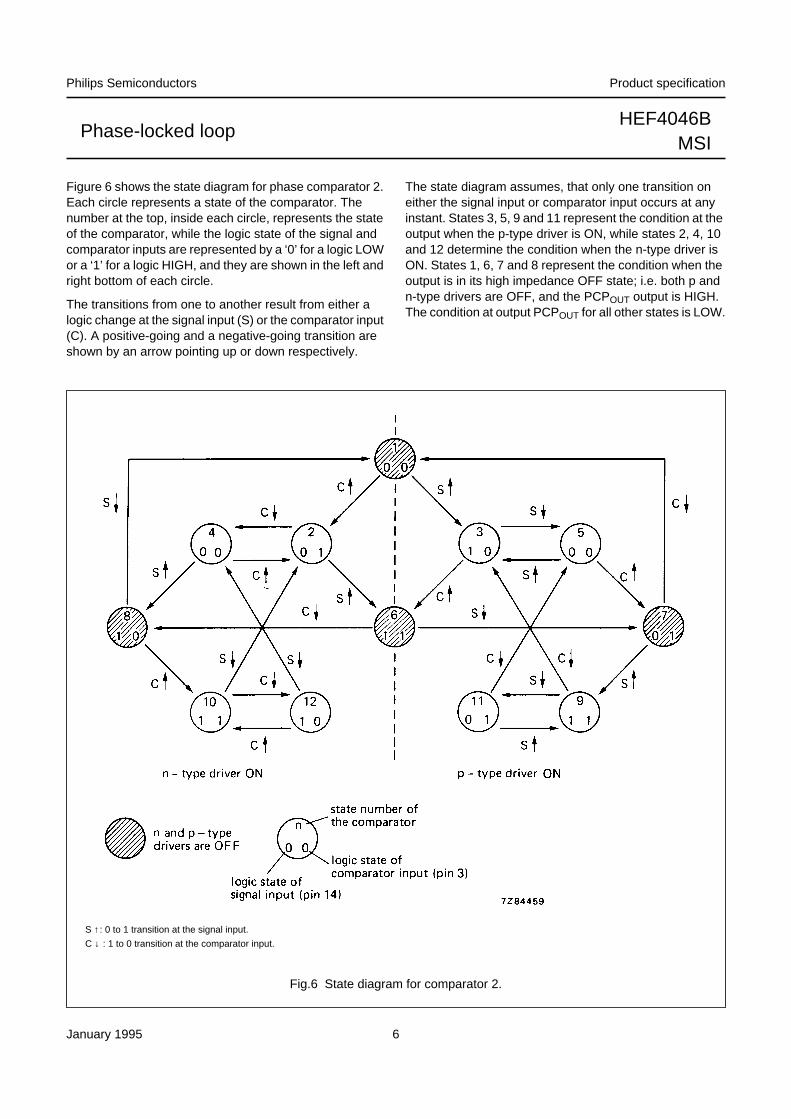
Figure 6 shows the state diagram for phase comparator 2.Each circle represents a state of the comparator. Thenumber at the top, inside each circle, represents the stateof the comparator, while the logic state of the signal andcomparator inputs are represented by a ‘0’ for a logic LOWor a ‘1’ for a logic HIGH, and they are shown in the left andright bottom of each circle.
The transitions from one to another result from either alogic change at the signal input (S) or the comparator input(C). A positive-going and a negative-going transition areshown by an arrow pointing up or down respectively.
The state diagram assumes, that only one transition oneither the signal input or comparator input occurs at anyinstant. States 3, 5, 9 and 11 represent the condition at theoutput when the p-type driver is ON, while states 2, 4, 10and 12 determine the condition when the n-type driver isON. States 1, 6, 7 and 8 represent the condition when theoutput is in its high impedance OFF state; i.e. both p andn-type drivers are OFF, and the PCPOUT output is HIGH.The condition at output PCPOUT for all other states is LOW.
Fig.6 State diagram for comparator 2.
S ↑: 0 to 1 transition at the signal input.
C ↓ : 1 to 0 transition at the comparator input.

January 1995 7
Philips Semiconductors Product specification
Phase-locked loopHEF4046B
MSI
DC CHARACTERISTICSVSS = 0 V
Notes
1. Pin 15 open; pin 5 at VDD; pins 3 and 9 at VSS; pin 14 open.
2. Pin 15 open; pin 5 at VDD; pins 3 and 9 at VSS; pin 14 at VDD; input current pin 14 not included.
AC CHARACTERISTICSVSS = 0 V; Tamb = 25 °C; CL = 50 pF; input transition times ≤ 20 ns
VDDV
SYMBOL
Tamb (°C)
−40 + 25 + 85
TYP. MAX. TYP. MAX. TYP. MAX.
Supply current 5 − − 20 − − − µA
(note 1) 10 ID − − 300 − − − µA
15 − − 750 − − − µA
Quiescent device 5 − 20 − 20 − 150 µA
current (note 2) 10 IDD − 40 − 40 − 300 µA
15 − 80 − 80 − 600 µA
VDDV
SYMBOL MIN. TYP. MAX.
Phase comparators
Operating supply voltage VDD 3 15 V
Input resistance 5 750 kΩat self-biasoperating point
at SIGNIN 10 RIN 220 kΩ15 140 kΩ
A.C. coupled input 5 150 mV peak-to-peak values;R1 = 10 kΩ; R2 = ∞;C1 = 100 pF; independentof the lock range
sensitivity 10 VIN 150 mV
at SIGNIN 15 200 mV
D.C. coupled input sensitivity
at SIGNIN; COMPIN 5 1,5 V
full temperature range
LOW level 10 VIL 3,0 V
15 4,0 V
5 3,5 V
HIGH level 10 VIH 7,0 V
15 11,0 V
Input current 5 7 µA
SIGNIN at VDDat SIGNIN 10 + IIN 30 µA
15 70 µA
5 3 µA
SIGNIN at VSS10 −IIN 18 µA
15 45 µA

January 1995 8
Philips Semiconductors Product specification
Phase-locked loopHEF4046B
MSI
Notes
1. Over the recommended component range.
VCO
Operating supply VDD 3 15 V as fixed oscillator only
voltage 5 15 V phase-locked loop operation
Power dissipation 5 150 µW fo = 10 kHz; R1 = 1 MΩ;R2 = ∞; VCOIN at 1⁄2 VDD;see also Figs 10 and 11
10 P 2500 µW
15 9000 µW
Maximum operating 5 0,5 1,0 MHz VCOIN at VDD;R1 = 10 kΩ; R2 = ∞;C1 = 50 pF
frequency 10 fmax 1,0 2,0 MHz
15 1,3 2,7 MHz
Temperature/ 5 0,220,30 %/°C no frequency offset(fmin = 0);see also note 1
frequency 10 0,040,05 %/°Cstability 15 0,010,05 %/°C
5 00,22 %/°C with frequency offset(fmin > 0);see also note 1
10 00,04 %/°C15 00,01 %/°C
Linearity 5 0,50 % R1 > 10 kΩ see Fig.13
10 0,25 % R1 > 400 kΩ and Figs 14
15 0,25 % R1 = 1 MΩ 15 and 16
Duty factor at 5 50 %
VCOOUT 10 δ 50 %
15 50 %
Input resistance at 5 106 MΩVCOIN 10 RIN 106 MΩ
15 106 MΩ
Source follower
Offset voltage 5 1,7 VRSF = 10 kΩ;VCOIN at 1⁄2 VDD
VCOIN minus 10 2,0 V
SFOUT 15 2,1 V
5 1,5 VRSF = 50 kΩ;VCOIN at 1⁄2 VDD
10 1,7 V
15 1,8 V
Linearity 5 0,3 %RSF > 50 kΩ;see Fig.13
10 1,0 %
15 1,3 %
Zener diode
Zener voltage VZ 7,3 V IZ = 50 µA
Dynamic resistance RZ 25 Ω IZ = 1 mA
VDDV
SYMBOL MIN. TYP. MAX.
January 1995 9
Philips Semiconductors Product specification
Phase-locked loopHEF4046B
MSI
DESIGN INFORMATION
VCO component selection
Recommended range for R1 and R2: 10 kΩ to 1 MΩ; for C1: 50 pF to any practical value.
1. VCO without frequency offset (R2 = ∞).
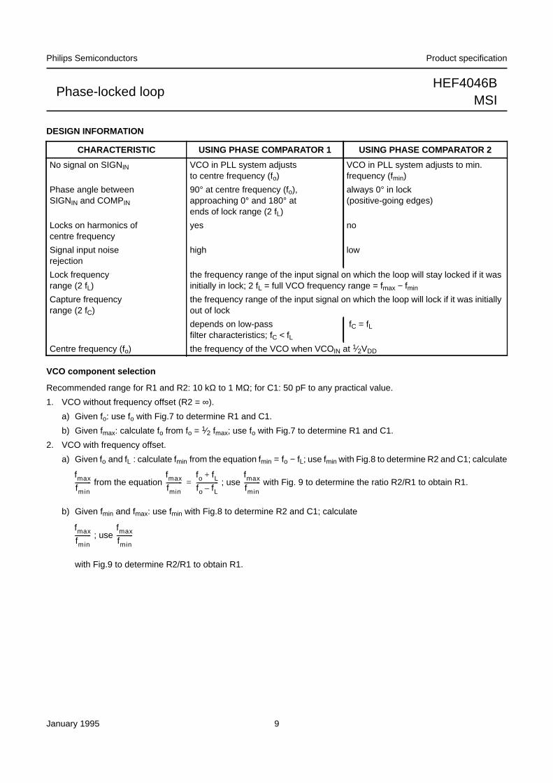
a) Given fo: use fo with Fig.7 to determine R1 and C1.
b) Given fmax: calculate fo from fo = 1⁄2 fmax; use fo with Fig.7 to determine R1 and C1.
2. VCO with frequency offset.
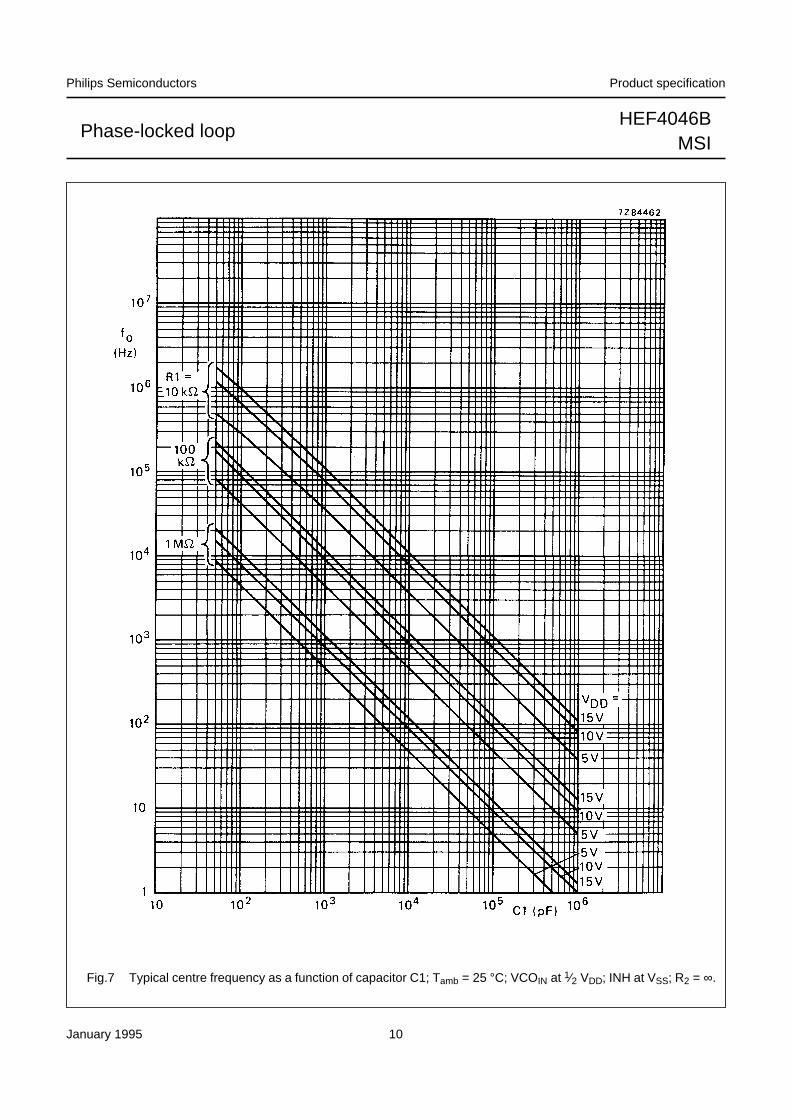
a) Given fo and fL : calculate fmin from the equation fmin = fo − fL; use fmin with Fig.8 to determine R2 and C1; calculate
b) Given fmin and fmax: use fmin with Fig.8 to determine R2 and C1; calculate
with Fig.9 to determine R2/R1 to obtain R1.
CHARACTERISTIC USING PHASE COMPARATOR 1 USING PHASE COMPARATOR 2
No signal on SIGNIN VCO in PLL system adjuststo centre frequency (fo)
VCO in PLL system adjusts to min.frequency (fmin)
Phase angle betweenSIGNIN and COMPIN
90° at centre frequency (fo),approaching 0° and 180° atends of lock range (2 fL)
always 0° in lock(positive-going edges)
Locks on harmonics ofcentre frequency
yes no
Signal input noiserejection
high low
Lock frequencyrange (2 fL)
the frequency range of the input signal on which the loop will stay locked if it wasinitially in lock; 2 fL = full VCO frequency range = fmax − fmin
Capture frequencyrange (2 fC)
the frequency range of the input signal on which the loop will lock if it was initiallyout of lock
depends on low-passfilter characteristics; fC < fL
fC = fL
Centre frequency (fo) the frequency of the VCO when VCOIN at 1⁄2VDD
fmax
fmin----------- from the equation
fmax
fmin-----------
fo fL+
fo fL–--------------- ; use
fmax
fmin----------- with Fig. 9 to determine the ratio R2/R1 to obtain R1.=
fmax
fmin----------- ; use
fmax
fmin-----------
January 1995 10
Philips Semiconductors Product specification
Phase-locked loopHEF4046B
MSI
Fig.7 Typical centre frequency as a function of capacitor C1; Tamb = 25 °C; VCOIN at 1⁄2 VDD; INH at VSS; R2 = ∞.
January 1995 11
Philips Semiconductors Product specification
Phase-locked loopHEF4046B
MSI
Fig.8 Typical frequency offset as a function of capacitor C1; Tamb = 25 °C; VCOIN at VSS; INH at VSS; R1 = ∞.

January 1995 12
Philips Semiconductors Product specification
Phase-locked loopHEF4046B
MSI
Fig.9 Typical ratio of R2/R1 as a function of the ratio fmax/fmin.
January 1995 13
Philips Semiconductors Product specification
Phase-locked loopHEF4046B
MSI
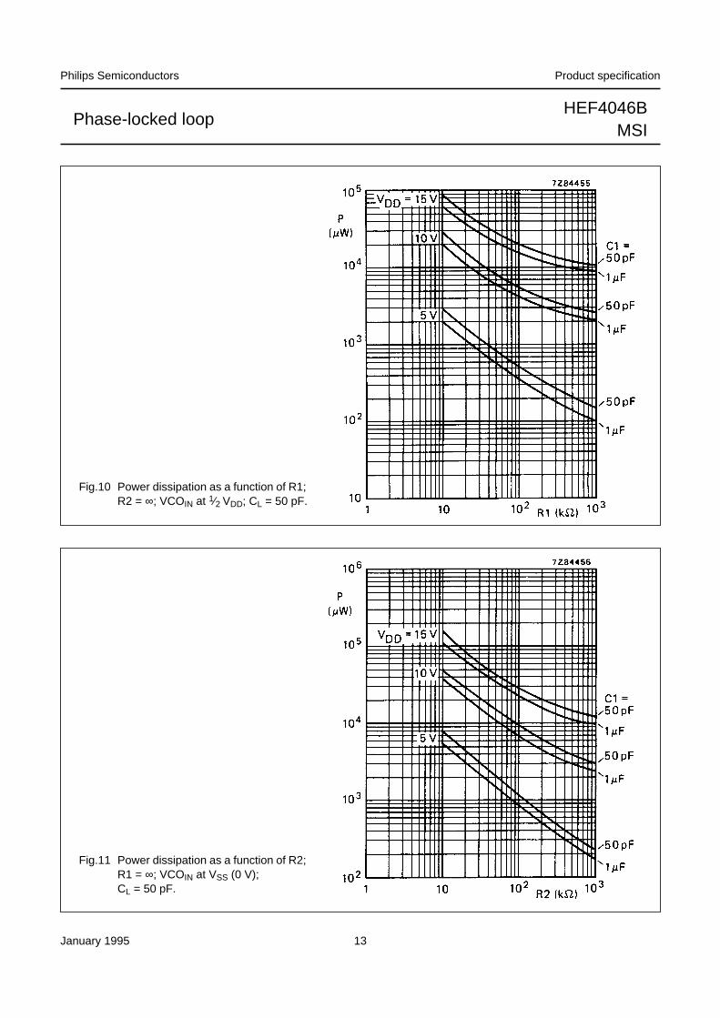
Fig.10 Power dissipation as a function of R1;R2 = ∞; VCOIN at 1⁄2 VDD; CL = 50 pF.
Fig.11 Power dissipation as a function of R2;R1 = ∞; VCOIN at VSS (0 V);CL = 50 pF.

January 1995 14
Philips Semiconductors Product specification
Phase-locked loopHEF4046B
MSI
Fig.12 Power dissipation of source follower as afunction of RSF; VCOIN at 1⁄2 VDD; R1 = ∞ ;R2 = ∞ .
Fig.13 Definition of linearity (see AC characteristics).
For VCO linearity:
Figure 13 and the aboveformula also apply tosource follower linearity:substitute VSF OUT for f.
∆V = 0,3 V at VDD = 5 V∆V = 2,5 V at VDD = 10 V∆V = 5 V at VDD = 15 V
f′o
f1 f2+
2---------------=
l in.f′o fo–
f′o
---------------- 100%×=

January 1995 15
Philips Semiconductors Product specification
Phase-locked loopHEF4046B
MSI
Fig.14 VCO frequency linearity as a function of R1;R2 = ∞; VDD = 5 V.
Fig.15 VCO frequency linearity as a function of R1;R2 = ∞; VDD = 10 V.
Fig.16 VCO frequency linearity as a function of R1;R2 = ∞; VDD = 15 V.