ece2029: introduction to digital circuit design lab 1 ...sjarvis/ece2029_smj/lab1_b15.pdfsequential...
TRANSCRIPT

ECE2029: Introduction to Digital Circuit Design
Lab 1 – Introduction to Xilinx Vivado Design Environment
ObjectiveAfter completion of this lab exercise you will be able to use the Vivado logic design environment to capture, simulate, test, and download a logic circuit to a Basys 3 Board.
Design Flow OverviewThe heart (brains?) of the Digilent Basys 3 development boards which we'll be using in lab is the Xilinx Artix FPGA. An FPGA is a type of programmable logic device – a FieldProgrammable Gate Array. Conceptually, an FPGA contains thousands and thousands of logic gates whose inputs and outputs can be connected to or disconnected from each otheror to/from inputs and output devices like switches and LEDs by applying “programming voltages”. If a given interconnection is “programmed” with a logic 1 then a connection ismade otherwise it is not. Thus, when we "program" an FPGA we ARE NOT WRITING SOFTWARE but in essence specifying the hardware connections between logic components – we are wiring the circuit! Below are the steps used to implement modern logic designs using programmable logic devices.
Design Entry: You enter your design into the system through through an HDL(Hardware Description Languages such as Verilog, VHDL or System C). In general, yourdesign may include different individual logic gates, combinational logic blocks, and/orsequential logic blocks.
Verification: Simulators are used for functional and timing verification of the design.Functional simulation verifies the logic behavior of the system without any knowledge ofthe underlying target device and does not provide any timing information. Timingsimulation provides various timing analysis after the design has been compiled for aspecific target device.
Implementation: Design tools like Vivado translate your design into an optimized formatsuitable to your target device. The output of this step is a bit stream file (or a .bit file) thatcan be downloaded into the hardware. The bit stream is the list of connections that are tobe made within the FPGA.
Figures 1&2 show more detailed design flow diagrams for FPGA devices. As mentionedabove, our projects are targeted for Xilinx Artix 7 FPGAs.
Pre-lab AssignmentUsually, laboratory exercises will have pre-lab assignments which are to be completed before your lab session and must be signed-off by the TA during your lab session. Pre-labs help you to become oriented to the problem before you enter lab, help complete your design in advance and prevent wasting time in lab. This first lab is a straight forward tutorial and does not have a pre-lab.

Figure 1
Figure 2
AssignmentIn this first lab you will start by impementing the basic logic gates AND, OR, NOT and the compound exclusive OR gate (XOR) and verify their truth tables. Then you will implement a multi-gate circuit. You will do this using the Verilog hardware description language.
1. Start Vivado Design Suite by clicking on Vivado icon and then selecting Create New Project from the menu.
2. Enter a project name. You should use your network drive as the project location for your files. Make sure there are no spaces in the folder name that you create foryour work. If you must create you project on the local disk be sure to back it up toyour network drive when you’re done at the end of lab. Lab machines can be re-imaged at any time and you could lose your work if it is not on your network drive!


3. Click Next and then select the RTL project type. Be sure to check the “Do not specify sources at this time” box and click Next:
4. Click next and select the correct Xilinx Artix 7 FPGA that is on the Basys3 board (XC7A35T-1CPG236C)
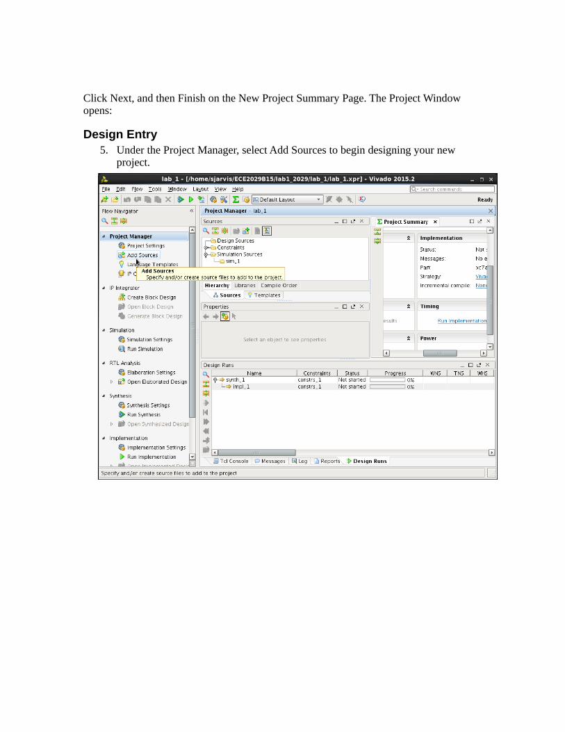
Click Next, and then Finish on the New Project Summary Page. The Project Window opens:
Design Entry 5. Under the Project Manager, select Add Sources to begin designing your new
project.

6. Select Next and then select Create File (click on the + symbol) and enter the file name for the circuit.
7. Then click OK and Finish. We can now specify the inputs and outputs to create our AND, OR, NOT and XOR gates. We will use three slide switches as inputs

and 4 LEDs to display the outputs of each gate. Inputs A and B will be the inputs to the AND, OR and XOR gates and C will be the input to the NOT gate.
8. Click OK. Back in the Project Manager Sources window double-click t he new and_or_not_xor.v file and you will then see the Verilog file appear in the window on the right. Add your name and a description of this file to the header description. You should ALWAYS complete the comment bock at the top of each Verilog module that you write. This is basic professionalism.
9. We can now add the Verilog statements to design our gates. Enter the code below to your and_or_not_xor.v file.

10. Now we can synthesize the design. Click Run Synthesis in the Project Manager window. After synthesis is complete there should be no errors or warnings reported. If you open the synthesized design you can see a device level representation (this is mostly empty since we just have a very simple design that only uses a tiny, tiny fraction of the available FPGA resources).
11. You can also look at a schematic representation to see the input and output buffersand the Look Up Tables (LUT) used. LUTs can be used to implement any truth table with a certain number of inputs. Notice that since AND, OR and XOR all have A and B as inputs they are implemented in the same LUT.

12. Before we can implement the design we need to specify the FPGA pins that will be used for the SW inputs and LED outputs. The Digilent Basys 3 Re ference Manual provides detailed information about the Basys3 Starter board. Figure 16 shows the overall architecture of the board with its major components. Basys3 board provides sixteen sliding switches (SW0-SW15) and five push buttons (BTN5-BTN0) that can be used as inputs. Each of these switches is connected to an associated IO pin of the FPGA. Figure 16 in the Basys2 Reference Manual shows to which pins these digital IO devices are connected. Both the slide switches and push buttons are active high, in other words when they are “on” theyconnect VCCO = Logic 1 to the FPGA IO pin. Note that there is no de-bouncing circuitry for these inputs. There sixteen surface mounted LED’s on the board that can be used as outputs (LD15-LD0). The LED’s are all active high, so to turn an LED ON you need to apply a logic high to the corresponding IO pin of the FPGA.Look at the Basys 3 manual to determine the FPGA pins connected to switches SW0, SW1 and SW2 and LEDs LED0, LED1, LED2 and LED3.
13. Next click Add Sources and select Add or create constraints.

And name the constraints file.
14. In the sources window select the constraints file through the hierarchy Constraints => constrs_1 => and_or_not_xor.xdc. We can now add location constraints for all the inputs and outputs . These constraints specify the pins to usefor each signal and what type of interface. You can download a copy of the Basys3 XDC constraints from the Digilent website – just copy the pins you are using for the design. Or, just type in this file and modify it as needed . Remember

the listing of pins (e.g. W17) to which the LED and switches are connected are given in the Basys 3 manual.
Generating a Test-bench Waveform for Functional Verification
Functional (Behavioral) Simulation for Design VerificationIn this section you will learn how to create and use a Verilog Test Bench to verify the functional behavior of your design. Verilog is a simulation language as well as synthesis language. In a HDL simulation, the design you want to test is instantiated in the simulator(ISim). You will need to add the Verilog that asserts all input combinations you want to test. For our simple logic gates there are only 6 input combinations we need to consider (A=0 B=0, A=1 B=0, A=0 B=1, A=1 B=1 and C=0, C=1) so you can easily complete an “exhaustive test” of all possible inputs.
15. Under the Project Manager Simulation Sources, right click on sim_1(1) and Add Sources. Choose Add or create simulation sources. Create a file and name it tb_and_or_not_xor or similar. The tb stands for testbench.
16. Right click you new file and Set it as Top module. Double click on the file name to open it in the editor window and add the following Verilog code. Notice that your are instantiating the and_or_not_xor module you defined above as U1. We are using simulator input signals called aa, bb and cc as inputs A, B, and C respectively and have assigned simulator outputs out1, out2, out3, out4 as outAND, outOR, outXOR, and notC respectively. Then we set the values of aa, bband cc to the all the settings we wish to test.

17. Afterwards you will see your testbench in bold under sim_1 with the module and_or_not_xor under it.
18. Select your testbench file then click on Run Simulation then Run Behavioral Simulation. Vivado will whir and spin for a second before opening a simulation window in which you can't see a thing! In the simulation window hit the Run All button then click on the Zoom Fit button.

You should now see a timing diagram like this.
19. Are the outputs of the simulation as you expected them to be? Save a screen shotof this simulation result to show the TA and to include in your Lab report.

Synthesis & Simulation for Synthesis and Timing VerificationYou have completed your design entry and functional verification of your Verilog modulewithout any assumptions about the underlying target. In this section you will synthesize your design targeted for Basys3 FPGA device.
20. Under Design Sources, select your and_or_not_xor module then click Run Implementation. You will find there are two warnings after implementation. This is because we have not specified any timing constraints. For this simple combinational circuit we can ignore this.
21. Now select you testbench file and then Run Simulation/ Run Post-implementationTiming Simulation. Again, Vivado will go off and simulate and open a window which you can't read. Hit the Run All followed by the Zoom Fit button again.
22. This simulator models the expected propagation delays resulting from the actual lay-out of the gates and pin connections on the FPGA. You can see the propagation delays from the time an input changes until the corresponding changein output occurs. Hit the Zoom + button to see in more detail. What's going on justafter 200 ns? Check your testbench file. Notice that we changed aa=0 and bb=1 without a delay in between. Behaviorally, we wanted those inputs to change values exactly simultaneously. However, in the actual implementation that is not physically possible and both aa and bb must have been equal to 1 for a nanosecond and we see the slight “glitch” in the outputs. If you go back into your test bench and but a #100 after aa=00 and before bb=1 then this “glitch” will not occur in the post-implementation simulation.
23. Use the zoom and the cursor measuring tools on the toolbar to measure the propagation delay of your design as it is actually laid out for implementation on

the Artix FPGA. Zoom in to one of the transitions of each output. Take screen shots and measure the delay for the Inverter to include in your lab report.
Implementation and Downloading
24. Under Program and Debug click Generate Bitstream. This generates the downloadable bitstream file (*.bit).
25. The Next step is to program the FPGA with the bitsream. On the Basys3 board make sure that JP1 is set to the JTAG mode and connect the USB cable to the board and turn on the power.
26. Select the Hardware Manager in the Project Manager and select Open Target and then Auto Connect. You should see the Xilinx xc7a35t_0 in the Hardware Window.

27. Click on Program Device and select the and_or_not_xor.bit bitstream file (automatically filled in). Then select Program (ignore the warning about the missing debug core and the rule violation).
28. Now you can test your design by toggling SW0, SW1 and SW2 and see the various outputs on LD3-LD0. Try different combination of inputs and make sure

that your design works properly. Demonstrate your and_or_not_xor circuit to the TA for Sign-off CREDIT!!
Programming the Serial Flash
29. Close the Hardware manager to go back to the Project Manager window.
30. The FPGA is a volatile device so the bit file will be lost after power is removed. We can also choose to write the program to the QSPI serial flash on the Basys3 board. Then the bit file will load from the flash on power up.
31. First we need to create a bin file to be able to program the serial flash.
32. Click on the Bitstream Settings in the Program and Debug section of the Project manager and Select the bin_file option.
33. Click OK then click on Generate Bitstream. After generation, if you look in the lab_1 => lab_1.runs => impl_1 directory you will see a .bit file and a .bin file.
34. Use the Hardware Manager to connect to the Basys3 board then right-mouse clickon the FPGA and select Add Configuration Memory Device. We now need to select the serial flash device that is on the Basys3 board. Select Spansion as the Manufacturer, then select the 32Mb device and OK. Then click OK for the pop-up.
35. Select the Configuration File (and_or_not_xor.bin) in the impl_1 directory and click OK. Note: this will erase any existing design in the QSPI flash (including the configuration file that shipped with the Basys3 board). The QSPI Flash will then be programmed with the and_or_not_xor.bin file. Once programmed, you can power off the Basys3 board and change the JP1 jumper mode from JTAG to QSPI. Power back on the board and after a few seconds the Done LED will turn

on indicating that your design has been automatically loaded into the FPGA from the serial flash. You can verify your and_or_not_xor design by moving the slider switches and observing the leds as before.
36. Write a high quality lab report. See Sign-off page for details!

Summary· You should be able to describe a Design flow for digital systems· You learned how to use Vivado Design Studio tools to enter a design, synthesize,
and download your implementation to a target board· You learned how to use ISim simulator to create stimulus signals, verify
functional and timing behavior of a digital system.
ALL TEAM MEMBERS SHOULD SAVE THIS PROJECT TO YOUR NETWORK DRIVES RIGHT NOW!!!

ECE2029 Lab 1 Sign-Off Sheet
Make sure lab the instructor/TAs initials and dates each part. Attach this sheet and the Grading Rubric to your team's lab report!
Your Name: ECE BOX #:
Lab Partner: ECE BOX #:
Date Performed:
Demonstrated correctly:
• Verilog AND-OR-NOT-XOR Behavioral Simulation_______________ (5pts)
• Verilog AND-OR-NOT-XOR Timing Simulation___________________ (5 pts)
• Verilog AND-OR-NOT-XOR circuit (.bit file) ____________________ (10pts)
• Verilog AND-OR-NOT-XOR circuit (.bin file)____________________ (10 pts)
• TA Questions _____________________ (5 pts)
• Report ____________________ (25 pts) (including Verilog & test bench code and simulation screen shots)

Lab 1: Introduction to Xilinx Webpack Report Grading Rubric
Review Item Comments Points (max) 1) Prelab complete and thoughtful --- N/A
2) Introduction effectively presents the (5)objectives and purpose of the lab.
3) Methodology gives enough details to allow for replication of procedure. (You may assumelab assignment is available. You do not have toregurgitate the lab instructions). (5)
4) Discussion opens with an effective statement on the goals of the lab, backs up statement with reference to appropriate findings, provides sufficient and logical explanation for the statement, addresses other issues pertinent to lab.
5) Results opens with effective statement of (5)overall findings, presents visuals clearly and accurately, presents findings clearly and with sufficient support. You MUST include screen shots of the test bench results for each part of the lab.
Conclusion convincingly describes what has been learned in the lab.
6) Other: (10) References are included.
Tables and figures are formatted.
Grammar and spelling are correct
Report is written clearly and to the point.
Overall, the student... • has successfully demonstrated what the lab was designed to teach
• demonstrates clear and thoughtful scientific inquiry
• has accurately measured and analyzed data for lab findings
Total: ___________ (25)