modeling and simulation of high speed pll based … · index terms—behavioral modeling, ... ahmed...
TRANSCRIPT
Abstract— In this paper, behavioral model of a high speed
Phase Locked Loop (PLL) based frequency synthesizer is
presented which is used for Radio Frequency Identifier (RFID)
in UHF carrier. The results are validated through System
Vision simulation using Very High Speed Integrated Circuit
Hardware Description Language-Analog Mixed Signal (VHDL-
AMS). PLL consists of a low jitter PLL employing a Voltage
Controlled Crystal Oscillator (VCXO). The advantage of using
low-jitter wide-band PLL is excellent performance in terms of
jitter and frequency locking. Simulation results are in good
agreement with theoretical calculations. Radio Frequency
Identification (RFID) uses RF radiation to identify physical
objects. With decreasing integrated circuit (IC) cost and size,
RFID applications are becoming economically feasible and
gaining popularity. In UHF passive RFID tag, communication
system needs low-jitter signal for UHF transmitter and receiver
to minimize the error in data stream.
Index Terms—Behavioral Modeling, Frequency Synthesizer,
Phase Locked loop, RFID and VHDL-AMS.
I. INTRODUCTION
hase Locked Loops (PLLs) are widely used as an
important building block of many circuits and systems
[1]–[2]. In this paper, a frequency synthesizer is used to
recover the data stream from the transmitted carrier. The
property of making its output frequency an exact multiple of
reference frequency makes PLL the ideal choice for
frequency synthesizers. The common method for frequency
synthesis is to lock a PLL to a multiple of some reference
frequency. PLL based frequency synthesizers are used in
wide range of telecommunication circuits. In this case we
used it in Radio Frequency Identification (RFID) system that uses
RF radiation to identify physical objects. Decreasing integrated
circuit (IC) costs and sizes, RFID applications are becoming
economically feasible and gaining popularity.
II. TYPES OF RFID
RFID systems can be classified according to the radio
frequency used, the type of modulation used to communicate
and the type of tag used in the system.
Manuscript received March 13, 2015; revised Manuscript received;
revised April 4, 2015.
Ahmed Telba is with King Saud university Electrical Engineering
Department Saudi Arabia (corresponding author e-mail: atelba@
ksu.edu.sa). Khalid Jamil is with PSATRI King Saud university (e-mail:
[email protected]). This work is supported by NPST program by King
Saud University, Project Number 12-ELE2462– 02).
Radio Frequency: The radio frequency is defined as the
frequency of the sine wave generated by the reader to send a
request to the tag. Carrier wave frequency is of primary
importance in determining data transfer rates. In practical
terms the rate of data transfer is influenced primarily by the
frequency of the carrier wave used to carry the data between
the tag and its reader. Generally speaking, higher the carrier
frequency, higher the data transfer that can be achieved.
Three frequency ranges are generally pre-defined in RFID
systems as low, intermediate (medium) and high as shown in
Table 1.
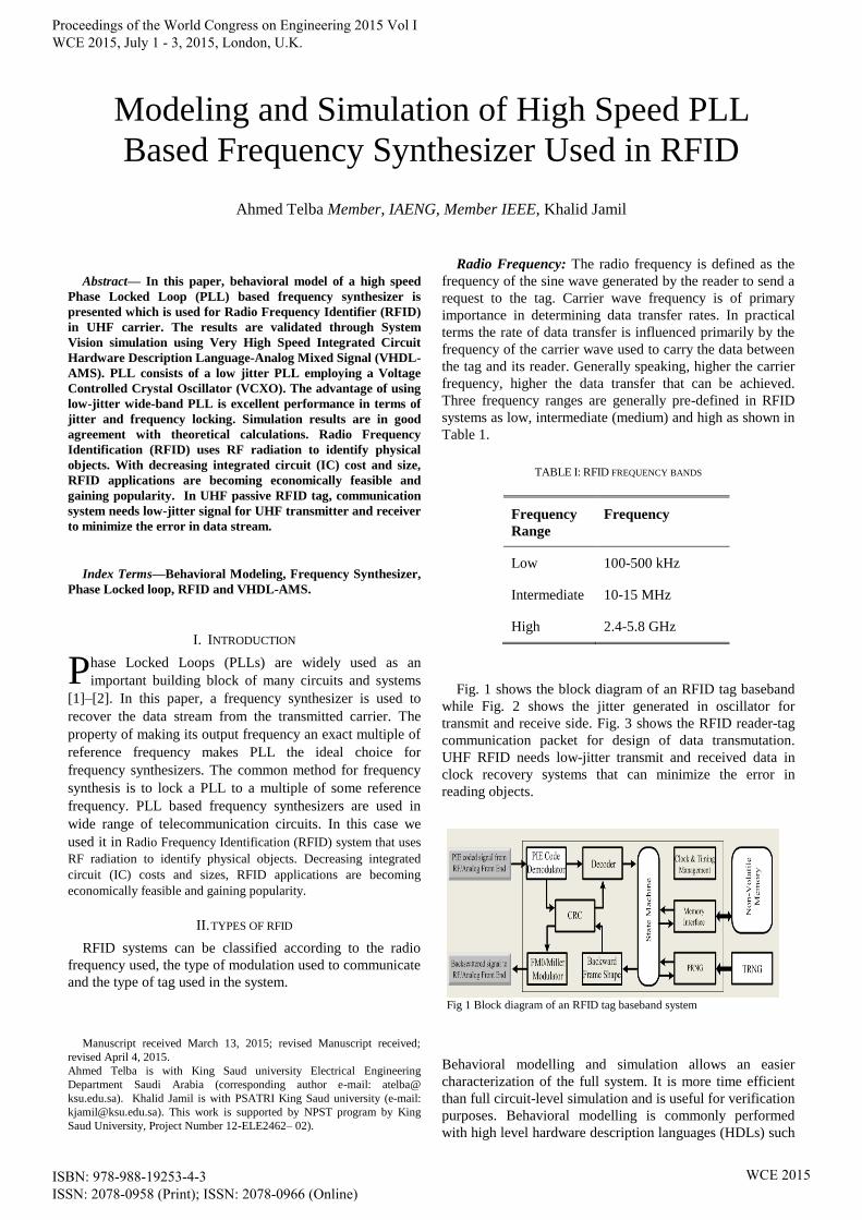
Fig. 1 shows the block diagram of an RFID tag baseband
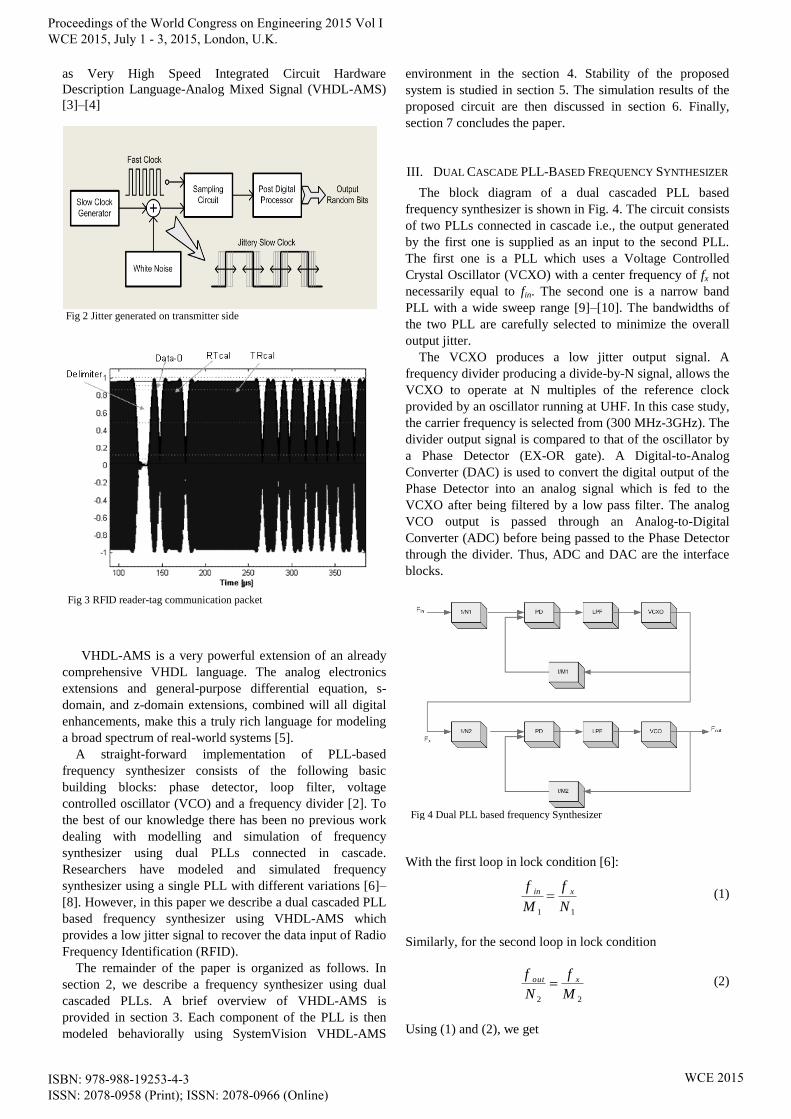
while Fig. 2 shows the jitter generated in oscillator for
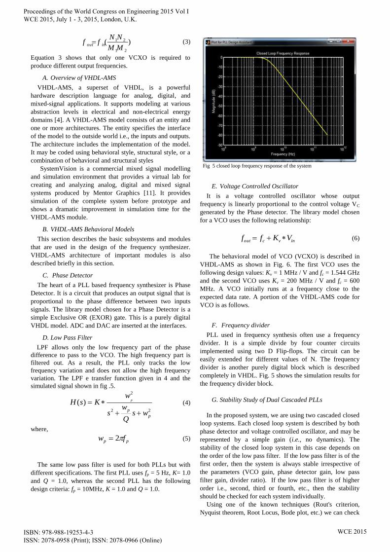
transmit and receive side. Fig. 3 shows the RFID reader-tag
communication packet for design of data transmutation.
UHF RFID needs low-jitter transmit and received data in
clock recovery systems that can minimize the error in
reading objects.
Behavioral modelling and simulation allows an easier
characterization of the full system. It is more time efficient
than full circuit-level simulation and is useful for verification
purposes. Behavioral modelling is commonly performed
with high level hardware description languages (HDLs) such
Modeling and Simulation of High Speed PLL
Based Frequency Synthesizer Used in RFID
Ahmed Telba Member, IAENG, Member IEEE, Khalid Jamil
P
TABLE I: RFID FREQUENCY BANDS
Frequency
Range
Frequency
Low 100-500 kHz
Intermediate 10-15 MHz
High 2.4-5.8 GHz
Fig 1 Block diagram of an RFID tag baseband system
Proceedings of the World Congress on Engineering 2015 Vol I WCE 2015, July 1 - 3, 2015, London, U.K.
ISBN: 978-988-19253-4-3 ISSN: 2078-0958 (Print); ISSN: 2078-0966 (Online)
WCE 2015
as Very High Speed Integrated Circuit Hardware
Description Language-Analog Mixed Signal (VHDL-AMS)
[3]–[4]
VHDL-AMS is a very powerful extension of an already
comprehensive VHDL language. The analog electronics
extensions and general-purpose differential equation, s-
domain, and z-domain extensions, combined will all digital
enhancements, make this a truly rich language for modeling
a broad spectrum of real-world systems [5].
A straight-forward implementation of PLL-based
frequency synthesizer consists of the following basic
building blocks: phase detector, loop filter, voltage
controlled oscillator (VCO) and a frequency divider [2]. To
the best of our knowledge there has been no previous work
dealing with modelling and simulation of frequency
synthesizer using dual PLLs connected in cascade.
Researchers have modeled and simulated frequency
synthesizer using a single PLL with different variations [6]–
[8]. However, in this paper we describe a dual cascaded PLL
based frequency synthesizer using VHDL-AMS which
provides a low jitter signal to recover the data input of Radio
Frequency Identification (RFID).
The remainder of the paper is organized as follows. In
section 2, we describe a frequency synthesizer using dual
cascaded PLLs. A brief overview of VHDL-AMS is
provided in section 3. Each component of the PLL is then
modeled behaviorally using SystemVision VHDL-AMS
environment in the section 4. Stability of the proposed
system is studied in section 5. The simulation results of the
proposed circuit are then discussed in section 6. Finally,
section 7 concludes the paper.
III. DUAL CASCADE PLL-BASED FREQUENCY SYNTHESIZER
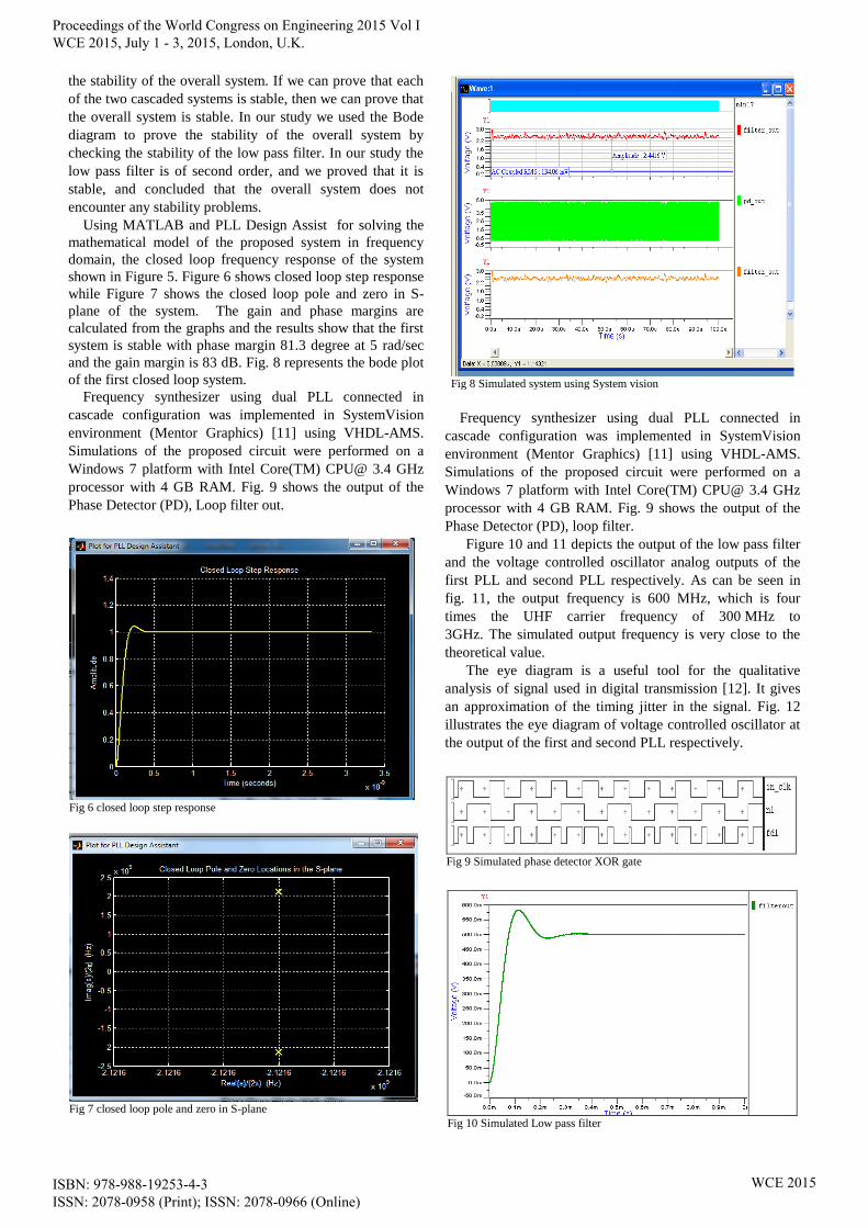
The block diagram of a dual cascaded PLL based
frequency synthesizer is shown in Fig. 4. The circuit consists
of two PLLs connected in cascade i.e., the output generated
by the first one is supplied as an input to the second PLL.
The first one is a PLL which uses a Voltage Controlled
Crystal Oscillator (VCXO) with a center frequency of fx not
necessarily equal to fin. The second one is a narrow band
PLL with a wide sweep range [9]–[10]. The bandwidths of
the two PLL are carefully selected to minimize the overall
output jitter.
The VCXO produces a low jitter output signal. A
frequency divider producing a divide-by-N signal, allows the
VCXO to operate at N multiples of the reference clock
provided by an oscillator running at UHF. In this case study,
the carrier frequency is selected from (300 MHz-3GHz). The
divider output signal is compared to that of the oscillator by
a Phase Detector (EX-OR gate). A Digital-to-Analog
Converter (DAC) is used to convert the digital output of the
Phase Detector into an analog signal which is fed to the
VCXO after being filtered by a low pass filter. The analog
VCO output is passed through an Analog-to-Digital
Converter (ADC) before being passed to the Phase Detector
through the divider. Thus, ADC and DAC are the interface
blocks.
With the first loop in lock condition [6]:
11 N
f
M
f xin (1)
Similarly, for the second loop in lock condition
22 M
f
N
f xout (2)
Using (1) and (2), we get
Fig 2 Jitter generated on transmitter side
Fig 3 RFID reader-tag communication packet
Fig 4 Dual PLL based frequency Synthesizer
Proceedings of the World Congress on Engineering 2015 Vol I WCE 2015, July 1 - 3, 2015, London, U.K.
ISBN: 978-988-19253-4-3 ISSN: 2078-0958 (Print); ISSN: 2078-0966 (Online)
WCE 2015
)(21
21
MM
NNff inout (3)
Equation 3 shows that only one VCXO is required to
produce different output frequencies.
A. Overview of VHDL-AMS
VHDL-AMS, a superset of VHDL, is a powerful
hardware description language for analog, digital, and
mixed-signal applications. It supports modeling at various
abstraction levels in electrical and non-electrical energy
domains [4]. A VHDL-AMS model consists of an entity and
one or more architectures. The entity specifies the interface
of the model to the outside world i.e., the inputs and outputs.
The architecture includes the implementation of the model.
It may be coded using behavioral style, structural style, or a
combination of behavioral and structural styles
SystemVision is a commercial mixed signal modelling
and simulation environment that provides a virtual lab for
creating and analyzing analog, digital and mixed signal
systems produced by Mentor Graphics [11]. It provides
simulation of the complete system before prototype and
shows a dramatic improvement in simulation time for the
VHDL-AMS module.
B. VHDL-AMS Behavioral Models
This section describes the basic subsystems and modules
that are used in the design of the frequency synthesizer.
VHDL-AMS architecture of important modules is also
described briefly in this section.
C. Phase Detector
The heart of a PLL based frequency synthesizer is Phase
Detector. It is a circuit that produces an output signal that is
proportional to the phase difference between two inputs
signals. The library model chosen for a Phase Detector is a
simple Exclusive OR (EXOR) gate. This is a purely digital
VHDL model. ADC and DAC are inserted at the interfaces.
D. Low Pass Filter
LPF allows only the low frequency part of the phase
difference to pass to the VCO. The high frequency part is
filtered out. As a result, the PLL only tracks the low
frequency variation and does not allow the high frequency
variation. The LPF e transfer function given in 4 and the
simulated signal shown in fig .5.
22
2
)(
p
pws
Q
ws
wKsH p
(4)
where,
pp fw 2 (5)
The same low pass filter is used for both PLLs but with
different specifications. The first PLL uses fp = 5 Hz, K= 1.0
and Q = 1.0, whereas the second PLL has the following
design criteria: fp = 10MHz, K = 1.0 and Q = 1.0.
E. Voltage Controlled Oscillator
It is a voltage controlled oscillator whose output
frequency is linearly proportional to the control voltage VC
generated by the Phase detector. The library model chosen
for a VCO uses the following relationship:
invcout VKff (6)
The behavioral model of VCO (VCXO) is described in
VHDL-AMS as shown in Fig. 6. The first VCO uses the
following design values: Kv = 1 MHz / V and fc = 1.544 GHz
and the second VCO uses Kv = 200 MHz / V and fc = 600
MHz. A VCO initially runs at a frequency close to the
expected data rate. A portion of the VHDL-AMS code for
VCO is as follows.
F. Frequency divider
PLL used in frequency synthesis often use a frequency
divider. It is a simple divide by four counter circuits
implemented using two D Flip-flops. The circuit can be
easily extended for different values of N. The frequency
divider is another purely digital block which is described
completely in VHDL. Fig. 5 shows the simulation results for
the frequency divider block.
G. Stability Study of Dual Cascaded PLLs
In the proposed system, we are using two cascaded closed
loop systems. Each closed loop system is described by both
phase detector and voltage controlled oscillator, and may be
represented by a simple gain (i.e., no dynamics). The
stability of the closed loop system in this case depends on
the order of the low pass filter. If the low pass filter is of the
first order, then the system is always stable irrespective of
the parameters (VCO gain, phase detector gain, low pass
filter gain, divider ratio). If the low pass filter is of higher
order i.e., second, third or fourth, etc., then the stability
should be checked for each system individually.
Using one of the known techniques (Rout's criterion,
Nyquist theorem, Root Locus, Bode plot, etc.) we can check
Fig 5 closed loop frequency response of the system
Proceedings of the World Congress on Engineering 2015 Vol I WCE 2015, July 1 - 3, 2015, London, U.K.
ISBN: 978-988-19253-4-3 ISSN: 2078-0958 (Print); ISSN: 2078-0966 (Online)
WCE 2015
the stability of the overall system. If we can prove that each
of the two cascaded systems is stable, then we can prove that
the overall system is stable. In our study we used the Bode
diagram to prove the stability of the overall system by
checking the stability of the low pass filter. In our study the
low pass filter is of second order, and we proved that it is
stable, and concluded that the overall system does not
encounter any stability problems.
Using MATLAB and PLL Design Assist for solving the
mathematical model of the proposed system in frequency
domain, the closed loop frequency response of the system
shown in Figure 5. Figure 6 shows closed loop step response
while Figure 7 shows the closed loop pole and zero in S-
plane of the system. The gain and phase margins are
calculated from the graphs and the results show that the first
system is stable with phase margin 81.3 degree at 5 rad/sec
and the gain margin is 83 dB. Fig. 8 represents the bode plot
of the first closed loop system.
Frequency synthesizer using dual PLL connected in
cascade configuration was implemented in SystemVision
environment (Mentor Graphics) [11] using VHDL-AMS.
Simulations of the proposed circuit were performed on a
Windows 7 platform with Intel Core(TM) CPU@ 3.4 GHz
processor with 4 GB RAM. Fig. 9 shows the output of the
Phase Detector (PD), Loop filter out.
H. Simulation Results
Frequency synthesizer using dual PLL connected in
cascade configuration was implemented in SystemVision
environment (Mentor Graphics) [11] using VHDL-AMS.
Simulations of the proposed circuit were performed on a
Windows 7 platform with Intel Core(TM) CPU@ 3.4 GHz
processor with 4 GB RAM. Fig. 9 shows the output of the
Phase Detector (PD), loop filter.
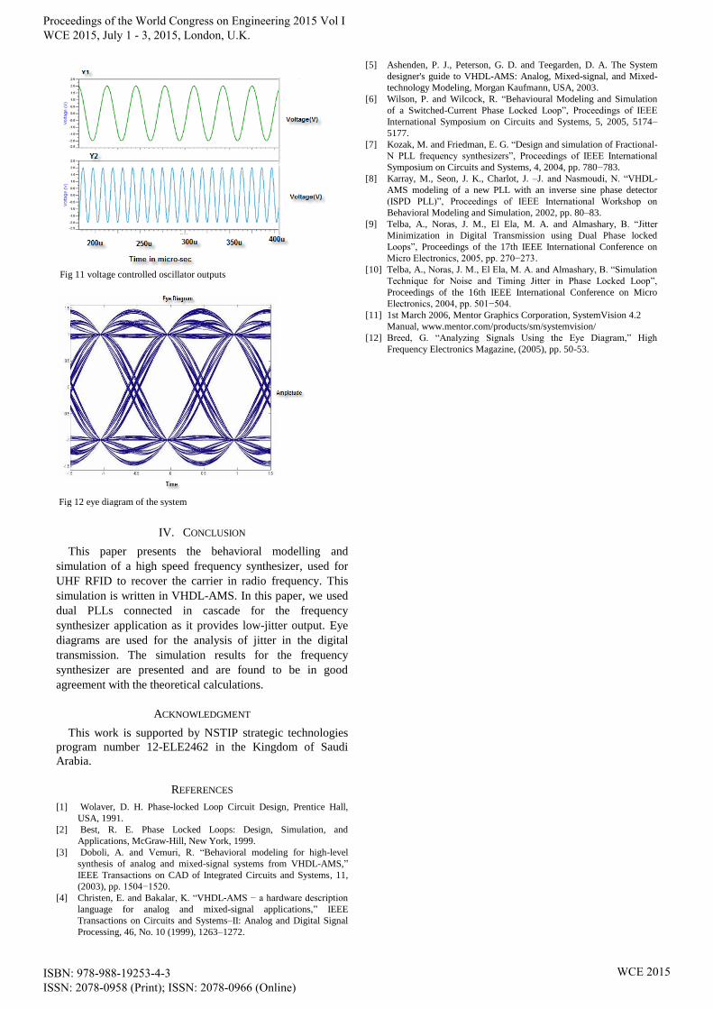
Figure 10 and 11 depicts the output of the low pass filter
and the voltage controlled oscillator analog outputs of the
first PLL and second PLL respectively. As can be seen in
fig. 11, the output frequency is 600 MHz, which is four
times the UHF carrier frequency of 300 MHz to
3GHz. The simulated output frequency is very close to the
theoretical value.
The eye diagram is a useful tool for the qualitative
analysis of signal used in digital transmission [12]. It gives
an approximation of the timing jitter in the signal. Fig. 12
illustrates the eye diagram of voltage controlled oscillator at
the output of the first and second PLL respectively.
Fig 6 closed loop step response
Fig 7 closed loop pole and zero in S-plane
Fig 8 Simulated system using System vision
Fig 9 Simulated phase detector XOR gate
Fig 10 Simulated Low pass filter
Proceedings of the World Congress on Engineering 2015 Vol I WCE 2015, July 1 - 3, 2015, London, U.K.
ISBN: 978-988-19253-4-3 ISSN: 2078-0958 (Print); ISSN: 2078-0966 (Online)
WCE 2015
IV. CONCLUSION
This paper presents the behavioral modelling and
simulation of a high speed frequency synthesizer, used for
UHF RFID to recover the carrier in radio frequency. This
simulation is written in VHDL-AMS. In this paper, we used
dual PLLs connected in cascade for the frequency
synthesizer application as it provides low-jitter output. Eye
diagrams are used for the analysis of jitter in the digital
transmission. The simulation results for the frequency
synthesizer are presented and are found to be in good
agreement with the theoretical calculations.
ACKNOWLEDGMENT
This work is supported by NSTIP strategic technologies
program number 12-ELE2462 in the Kingdom of Saudi
Arabia.
REFERENCES
[1] Wolaver, D. H. Phase-locked Loop Circuit Design, Prentice Hall,
USA, 1991.
[2] Best, R. E. Phase Locked Loops: Design, Simulation, and
Applications, McGraw-Hill, New York, 1999.
[3] Doboli, A. and Vemuri, R. “Behavioral modeling for high-level
synthesis of analog and mixed-signal systems from VHDL-AMS,”
IEEE Transactions on CAD of Integrated Circuits and Systems, 11,
(2003), pp. 1504−1520.
[4] Christen, E. and Bakalar, K. “VHDL-AMS − a hardware description
language for analog and mixed-signal applications,” IEEE
Transactions on Circuits and Systems–II: Analog and Digital Signal
Processing, 46, No. 10 (1999), 1263–1272.
[5] Ashenden, P. J., Peterson, G. D. and Teegarden, D. A. The System
designer's guide to VHDL-AMS: Analog, Mixed-signal, and Mixed-
technology Modeling, Morgan Kaufmann, USA, 2003.
[6] Wilson, P. and Wilcock, R. “Behavioural Modeling and Simulation
of a Switched-Current Phase Locked Loop”, Proceedings of IEEE
International Symposium on Circuits and Systems, 5, 2005, 5174–
5177.
[7] Kozak, M. and Friedman, E. G. “Design and simulation of Fractional-
N PLL frequency synthesizers”, Proceedings of IEEE International
Symposium on Circuits and Systems, 4, 2004, pp. 780−783.
[8] Karray, M., Seon, J. K., Charlot, J. –J. and Nasmoudi, N. “VHDL-
AMS modeling of a new PLL with an inverse sine phase detector
(ISPD PLL)”, Proceedings of IEEE International Workshop on
Behavioral Modeling and Simulation, 2002, pp. 80–83.
[9] Telba, A., Noras, J. M., El Ela, M. A. and Almashary, B. “Jitter
Minimization in Digital Transmission using Dual Phase locked
Loops”, Proceedings of the 17th IEEE International Conference on
Micro Electronics, 2005, pp. 270−273.
[10] Telba, A., Noras, J. M., El Ela, M. A. and Almashary, B. “Simulation
Technique for Noise and Timing Jitter in Phase Locked Loop”,
Proceedings of the 16th IEEE International Conference on Micro
Electronics, 2004, pp. 501−504.
[11] 1st March 2006, Mentor Graphics Corporation, SystemVision 4.2
Manual, www.mentor.com/products/sm/systemvision/
[12] Breed, G. “Analyzing Signals Using the Eye Diagram,” High
Frequency Electronics Magazine, (2005), pp. 50-53.
Fig 11 voltage controlled oscillator outputs
Fig 12 eye diagram of the system
Proceedings of the World Congress on Engineering 2015 Vol I WCE 2015, July 1 - 3, 2015, London, U.K.
ISBN: 978-988-19253-4-3 ISSN: 2078-0958 (Print); ISSN: 2078-0966 (Online)
WCE 2015