spatial atomic layer deposition (ald): a novel disruptive...
TRANSCRIPT
Spatial Atomic Layer Deposition (ALD): a novel disruptive technology Fred Roozeboom, Holst Centre-TNO, and TU Eindhoven A. Illiberi, R. Knaapen, P. Poodt, Holst Centre-TNO, Eindhoven, NL
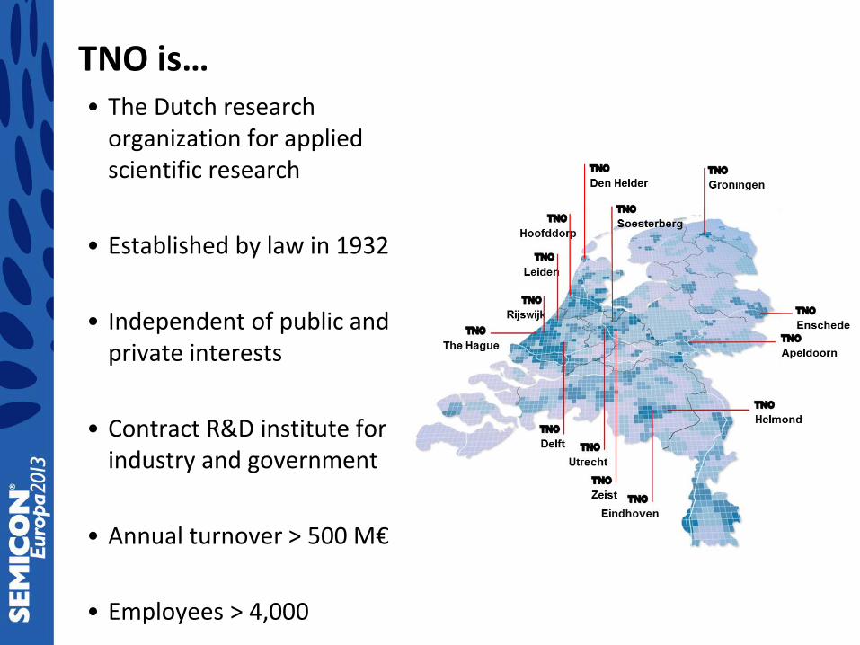
TNO is… • The Dutch research
organization for applied scientific research
• Established by law in 1932
• Independent of public and private interests
• Contract R&D institute for industry and government
• Annual turnover > 500 M€
• Employees > 4,000
© Holst Centre
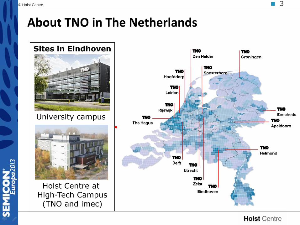
About TNO in The Netherlands
Sites in Eindhoven
University campus
Holst Centre at High-Tech Campus (TNO and imec)
< 3
© Holst Centre
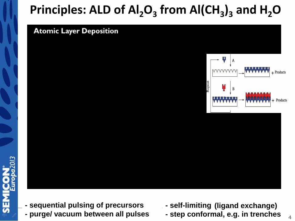
- self-limiting
- step conformal, e.g. in trenches
- sequential pulsing of precursors
- purge/ vacuum between all pulses (ligand exchange)
4
Principles: ALD of Al2O3 from Al(CH3)3 and H2O

© Holst Centre
What makes ALD a powerful technique
• Very high film quality
• No particles, no pinholes
• Thickness control on an atomic scale
• Superior conformality
• Ability to follow complex and 3D geometries
• Wide range of materials
• Oxides, nitrides, sulfides, ……
• Metals
• Hybrid organic – inorganic materials
• Even polymers
• But… s-l-o-w……
< 6
HfO2
Ge
10 nm
< 6
© Holst Centre
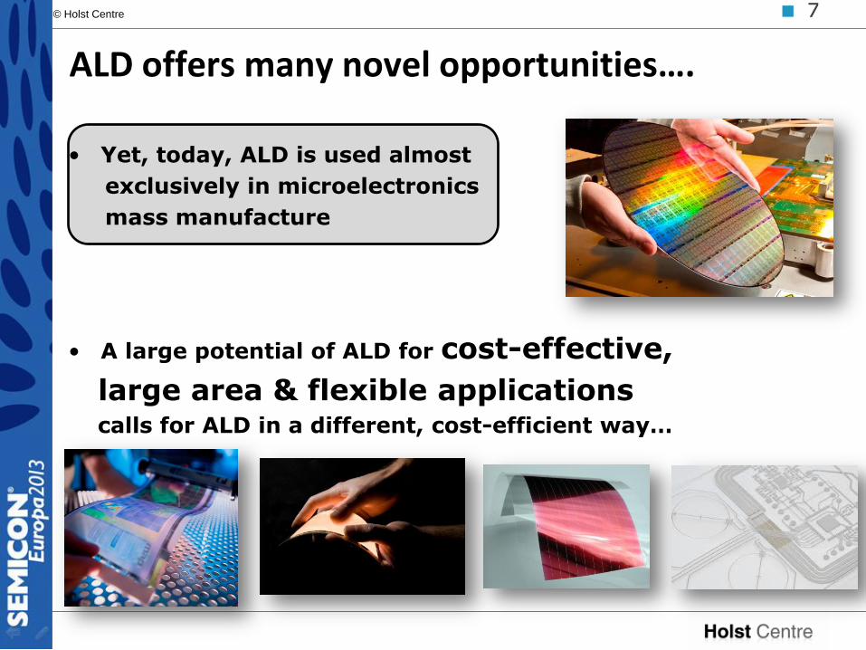
• Yet, today, ALD is used almost
exclusively in microelectronics
mass manufacture
• A large potential of ALD for cost-effective,
large area & flexible applications calls for ALD in a different, cost-efficient way…
ALD offers many novel opportunities….
< 7 < 7

© Holst Centre
Using ALD in a different, cost-efficient way…
< 8 < 8
• Faster
• Not limited by substrate size, material and flexibility
• Continuous, in-line
• Lower costs (e.g. precursor consumption)
• Atmospheric conditions
►Commercial use started only around 2008 :
Spatial (atmospheric) ALD
© Holst Centre
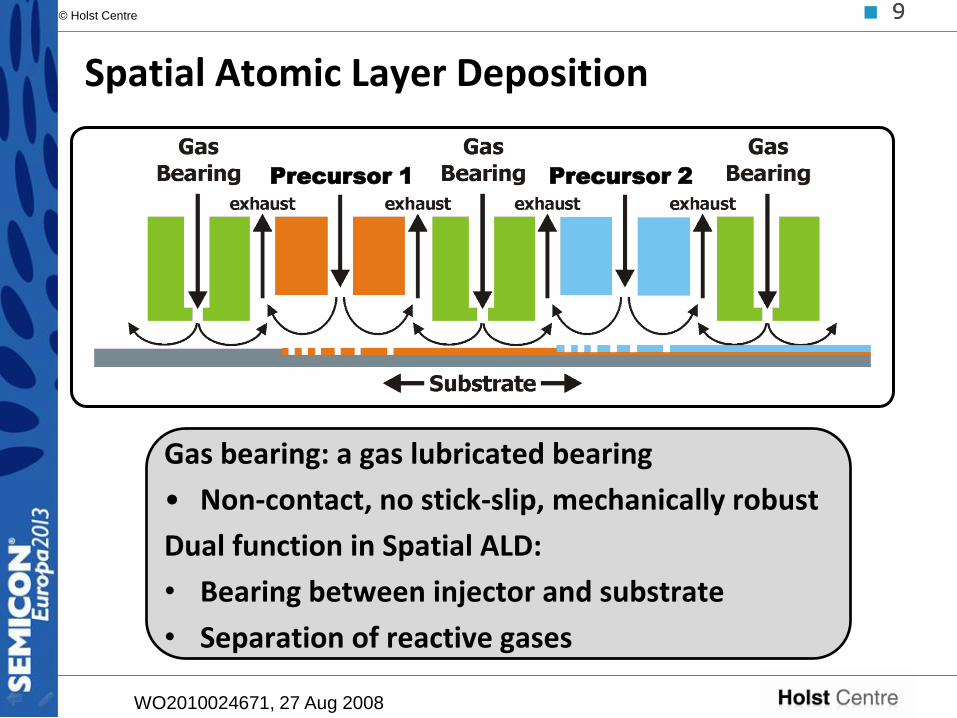
Spatial Atomic Layer Deposition Precursor 1 Precursor 2
WO2010024671, 27 Aug 2008
< 9
Gas bearing: a gas lubricated bearing
• Non-contact, no stick-slip, mechanically robust
Dual function in Spatial ALD:
• Bearing between injector and substrate
• Separation of reactive gases
< 9
© Holst Centre
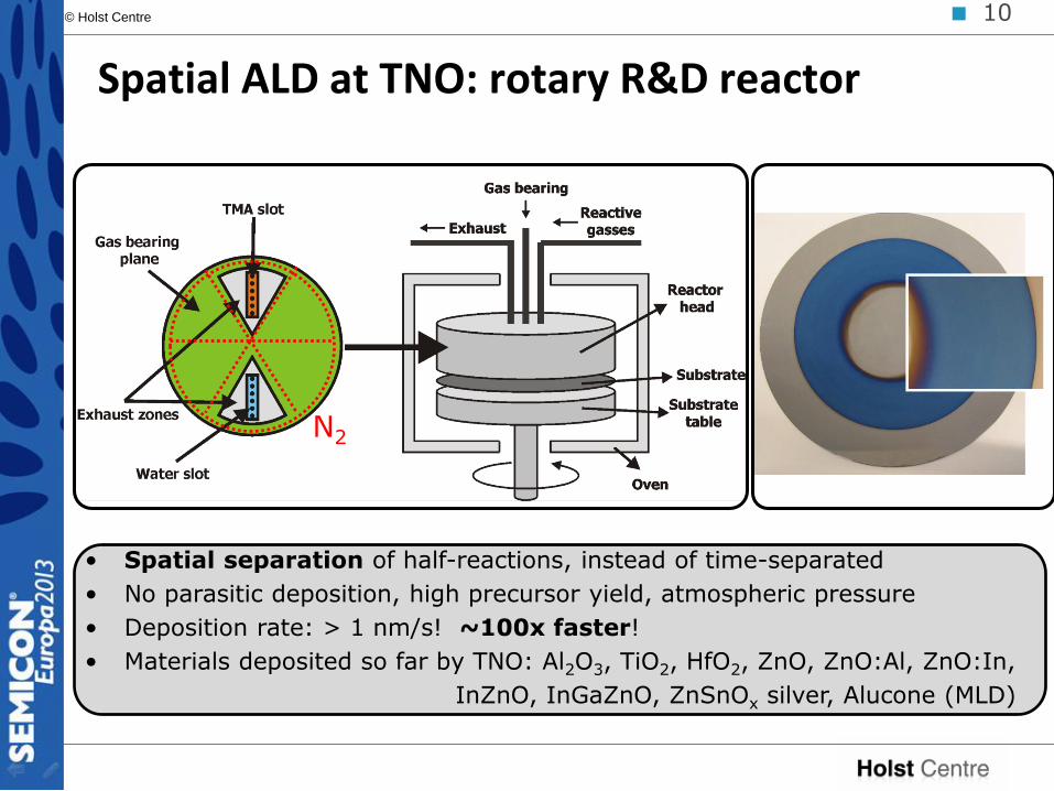
Spatial ALD at TNO: rotary R&D reactor
• Spatial separation of half-reactions, instead of time-separated
• No parasitic deposition, high precursor yield, atmospheric pressure
• Deposition rate: > 1 nm/s! ~100x faster!
• Materials deposited so far by TNO: Al2O3, TiO2, HfO2, ZnO, ZnO:Al, ZnO:In,
InZnO, InGaZnO, ZnSnOx silver, Alucone (MLD)
< 10
N2
© Holst Centre
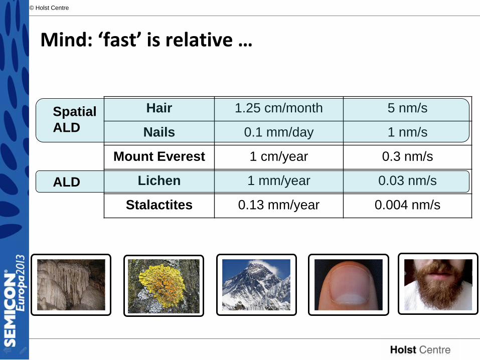
Mind: ‘fast’ is relative …
Hair 1.25 cm/month 5 nm/s
Nails 0.1 mm/day 1 nm/s
Mount Everest 1 cm/year 0.3 nm/s
Lichen 1 mm/year 0.03 nm/s
Stalactites 0.13 mm/year 0.004 nm/s
ALD
Spatial
ALD

© Holst Centre
• In-line spatial ALD reactors for c-Si solar cell manufacturing
< 13
Proven concept, commercially available
© Holst Centre
Opportunities for Spatial ALD
• Encapsulation & barriers (e.g. for OLEDs/OPV)
• Packaging
• Transparent conductors (e.g. for solar cells)
• Dielectric- and passivation layers and
amorphous oxide semiconductors (e.g. for TFTs)
• Light management (e.g. for solar cells and OLEDs)
• Hybrid or organic films by Molecular Layer Deposition Interface engineering (e.g. CIGS)
• Paper- or textile-based electronics
• Optical coatings
• Photovoltaics, OLEDs, displays, glazing,
energy storage, sensors, catalysis,…
< 14 < 14
© Holst Centre
Challenges to be addressed
• How fast and how large can we go?
• Uniformity
• Cost-efficiency
• How to get good performance at low deposition temperatures
• How to extend the process-toolbox
Plasma, ozone, UV, lasers, characterization,….
• How to do patterned deposition, and how small can we go ?
• Can we do Spatial MLD ?
• Can we use other precursors (cheaper, safer, effect of purity, ….)?
• How to do spatial ALD on polymer substrate ?
• ……..
< 15
© Holst Centre
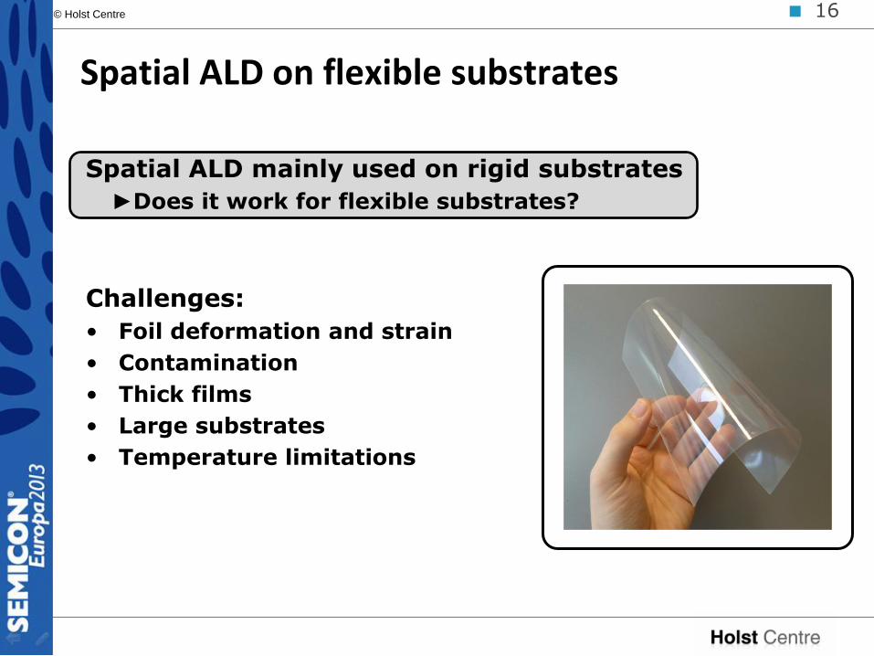
Spatial ALD on flexible substrates
Spatial ALD mainly used on rigid substrates
►Does it work for flexible substrates?
Challenges:
• Foil deformation and strain
• Contamination
• Thick films
• Large substrates
• Temperature limitations
< 16
© Holst Centre
17
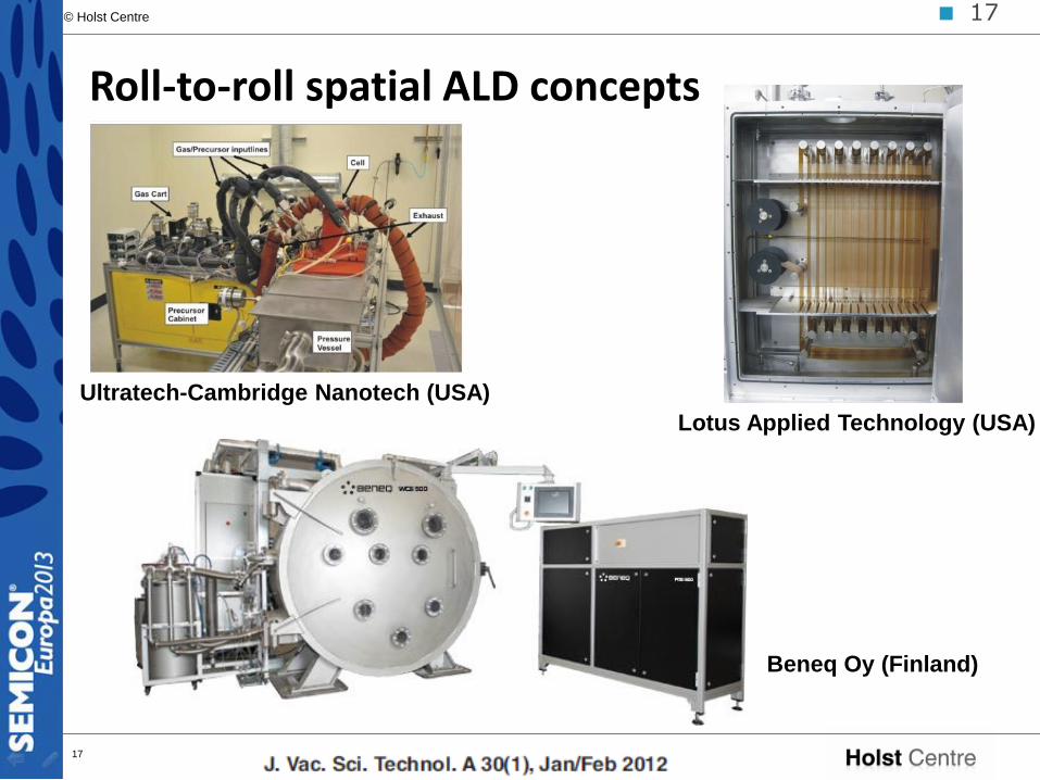
Roll-to-roll spatial ALD concepts
Beneq Oy (Finland)
Ultratech-Cambridge Nanotech (USA)
Lotus Applied Technology (USA)
< 17

© Holst Centre
Roll-to-roll spatial ALD: TNO’s approach
• Center piece: foil surrounding a drum with several reaction zones and gas-bearings
• Foil moves clockwise (slowly)
• Spatial ALD injector rotates counter-clockwise (fast)
• Combination ► high deposition rate
• Flows interrupted at bottom passage
• No mechanical contact on deposition side
• Flexibility in foil and layer thickness
• Compact
< 18
© Holst Centre
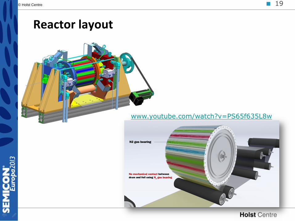
Reactor layout
< 19
www.youtube.com/watch?v=PS65f635L8w
© Holst Centre
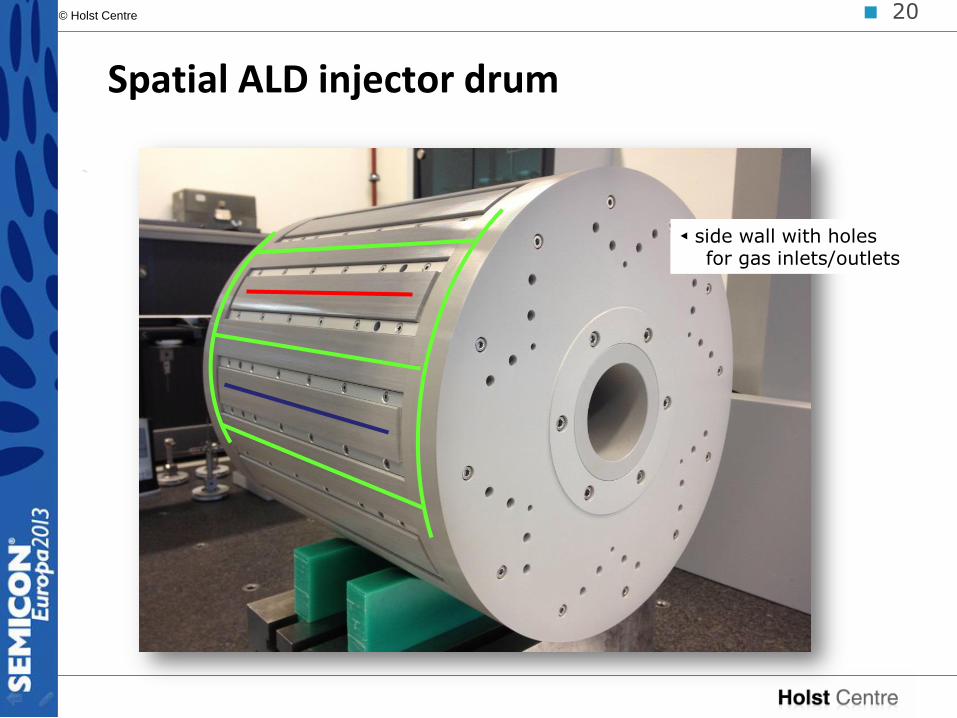
Spatial ALD injector drum
◄ side wall with holes for gas inlets/outlets
< 20
© Holst Centre
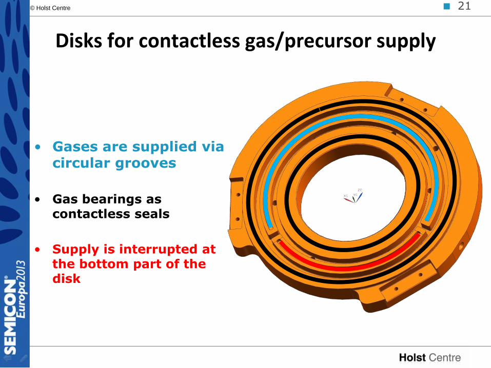
Disks for contactless gas/precursor supply
• Gases are supplied via circular grooves
• Gas bearings as contactless seals
• Supply is interrupted at the bottom part of the disk
< 21
© Holst Centre < 22
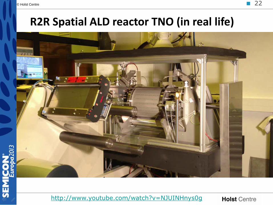
R2R Spatial ALD reactor TNO (in real life)
http://www.youtube.com/watch?v=NJUINHnys0g

© Holst Centre
First test results
• It works….
• Homogeneous Al2O3 deposition: thickness of ~25 nm at
1 m/min web speed and 60 rpm drum rotation
• 2Q2013: cleanroom environment installed
• Film property measurements are pending (e.g. WVTR)
< 23
12 days 20 oC/50 % RH 40 nm alumina on PEN WVTR = 1.5x10⁻⁵
g/m2/day
© Holst Centre
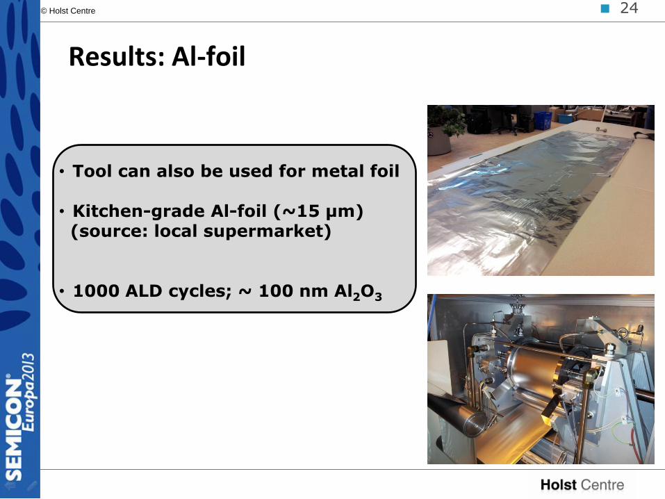
Results: Al-foil
• Tool can also be used for metal foil
• Kitchen-grade Al-foil (~15 µm) (source: local supermarket)
• 1000 ALD cycles; ~ 100 nm Al2O3
< 24
© Holst Centre
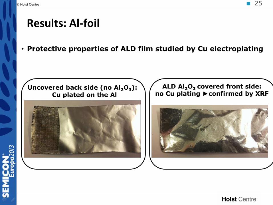
• Protective properties of ALD film studied by Cu electroplating
ALD Al2O3 covered front side: no Cu plating ►confirmed by XRF
< 25
Uncovered back side (no Al2O3): Cu plated on the Al
Results: Al-foil
© Holst Centre
Examples of applications
< 26

TMA H2O
space
N2 N2 TMA H2O N2 N2 …
Trench filling with spatial ALD of Al2O3 (200 oC, 1 atm.)
Courtesy:
SiO2
Si
~9 μm top
~4 μm
600 cycles (70 nm)
~0.12 nm/cycle
2 Hz rotary reactor
pTMA ~ 3 mbar
pH2O ~ 123 mbar
Step coverage ~ 80%
Time scale τ =13.5 ms
27
Al2O3
bottom
Al2O3
Al2O3 >100 :1
trenches

© Holst Centre
28
Thin film encapsulation • Water vapor infiltration: major reliability issue in large area electronics
(e.g. ZnO in CIGS, cathode in OLEDs, organic semiconductors)
• Encapsulant required to provide barrier against water diffusion
• Benchmarks:
Water Vapor Transmission Rate (WVTR, g/m2/day)
Oxygen Transmission rate (OTR, cm3/m2/day/atm)
Pinhole density
< 28
© Holst Centre
Encapsulation
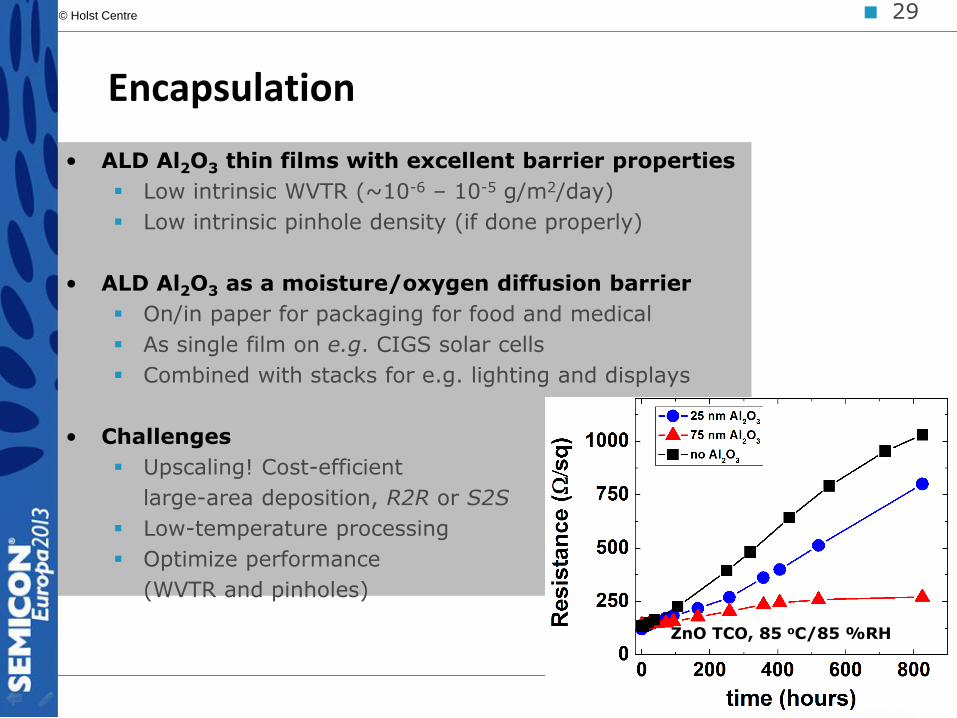
• ALD Al2O3 thin films with excellent barrier properties
Low intrinsic WVTR (~10-6 – 10-5 g/m2/day)
Low intrinsic pinhole density (if done properly)
• ALD Al2O3 as a moisture/oxygen diffusion barrier
On/in paper for packaging for food and medical
As single film on e.g. CIGS solar cells
Combined with stacks for e.g. lighting and displays
• Challenges
Upscaling! Cost-efficient
large-area deposition, R2R or S2S
Low-temperature processing
Optimize performance
(WVTR and pinholes)
< 29
ZnO TCO, 85 oC/85 %RH
© Holst Centre
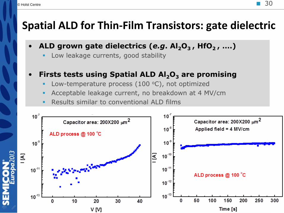
Spatial ALD for Thin-Film Transistors: gate dielectric
• ALD grown gate dielectrics (e.g. Al2O3 , HfO2 , ….)
Low leakage currents, good stability
• Firsts tests using Spatial ALD Al2O3 are promising
Low-temperature process (100 oC), not optimized
Acceptable leakage current, no breakdown at 4 MV/cm
Results similar to conventional ALD films
< 30

© Holst Centre
Spatial ALD of TFT channels: InGaZnO and ZnSnOx
• Method developed for making multi-component oxides by pre-mixing
No delta-doping/nanolaminates: uniform composition
Accurate control of composition and thickness
• Example: amorphous InGaZnO and ZnSnOx
Amorphous semiconductor, used as channel in TFT
First TFTs made with S-ALD InGaZnO !
Promising results, but further optimization required
< 31
© Holst Centre
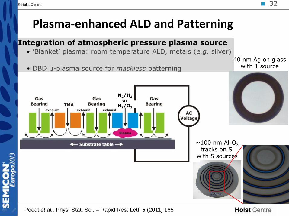
• Integration of atmospheric pressure plasma source • ‘Blanket’ plasma: room temperature ALD, metals (e.g. silver)
• DBD μ-plasma source for maskless patterning
Plasma-enhanced ALD and Patterning
Poodt et al., Phys. Stat. Sol. – Rapid Res. Lett. 5 (2011) 165
40 nm Ag on glass with 1 source
N2/H2 or
N2/O2
~100 nm Al2O3
tracks on Si with 5 sources
< 32
© Holst Centre
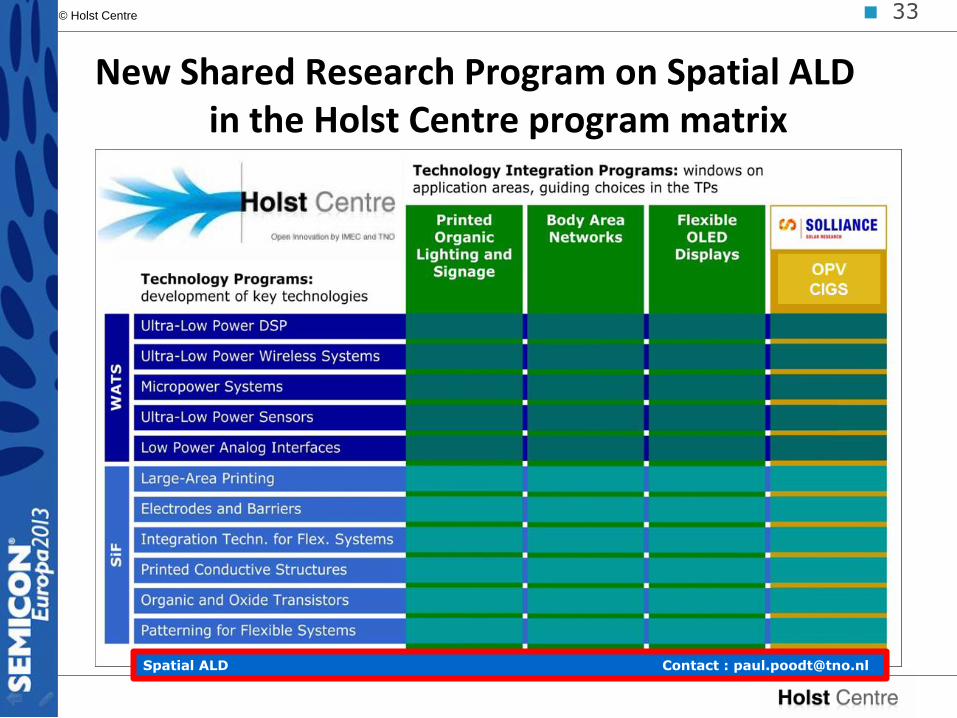
New Shared Research Program on Spatial ALD in the Holst Centre program matrix
< 33
Spatial ALD Contact : [email protected]
© Holst Centre
Acknowledgments
ALD team
Paul Poodt (Program Manager)
Almie van Asten (Project leader)
Andrea illiberi (InGaZnO)
Raymond Knaapen (R2R)
Frank Grob (R2R)
Mattijs van den Boer (R2R)
Fieke van den Bruele (MLD)
Mireille Smets (MLD)
Fred Roozeboom (ALD, RIE)
Students
Robert Sherpenborg (Al:ZnO)
Akhilc Sharma (InGaZnO)
Bart de Raadt (ZnSnOx)
Joep van Lieshout (R2R)
Sara Motahari
< 34
TNO (R2R)
Ruud Olieslagers
Dennis van de Berg
Adriaan Lankhorst
Joop van Deelen
Holst Centre (TFTs)
Brian Cobb
Ashutosh Tripathi
THANK YOU !

© Holst Centre < 35
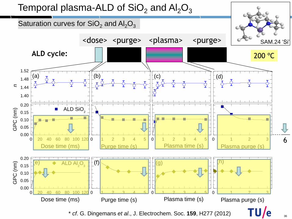
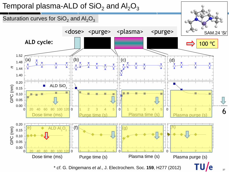
0 20 40 60 80 100 1200.00
0.05
0.10
0.15
0.20 ALD SiO
2
GP
C (
nm
)
Dose time (ms)
1.40
1.44
1.48
1.52
n
(a) (b)
0 1 2 3 4 5
Purge time (s)
0 1 2 3 4 5
Plasma time (s)
(c)
(d)
0 1 2 3
Plasma purge (s)
0 20 40 60 80 100 1200.00
0.05
0.10
0.15
0.20
ALD Al2O
3
GP
C (
nm
)
Dose time (ms)
(e)
0 1 2 3 4 5
(f)
Purge time (s)
0 1 2 3 4 5
(g)
Plasma time (s)
0 1 2 3
(h)
Plasma purge (s)
<dose> <purge> <plasma> <purge>
ALD cycle: 200 ºC
36
Saturation curves for SiO2 and Al2O3
Temporal plasma-ALD of SiO2 and Al2O3
‘Si’ SAM.24
* cf. G. Dingemans et al., J. Electrochem. Soc. 159, H277 (2012)
6
0 20 40 60 80 100 1200.00
0.05
0.10
0.15
0.20 ALD SiO
2
GP
C (
nm
)
Dose time (ms)
1.40
1.44
1.48
1.52
n
(a) (b)
0 1 2 3 4 5
Purge time (s)
0 1 2 3 4 5
Plasma time (s)
(c)
(d)
0 1 2 3
Plasma purge (s)
0 20 40 60 80 100 1200.00
0.05
0.10
0.15
0.20
ALD Al2O
3
GP
C (
nm
)
Dose time (ms)
(e)
0 1 2 3 4 5
(f)
Purge time (s)
0 1 2 3 4 5
(g)
Plasma time (s)
0 1 2 3
(h)
Plasma purge (s)
<dose> <purge> <plasma> <purge>
ALD cycle: 100 ºC
37
Saturation curves for SiO2 and Al2O3
Temporal plasma-ALD of SiO2 and Al2O3
‘Si’ SAM.24
* cf. G. Dingemans et al., J. Electrochem. Soc. 159, H277 (2012)
6
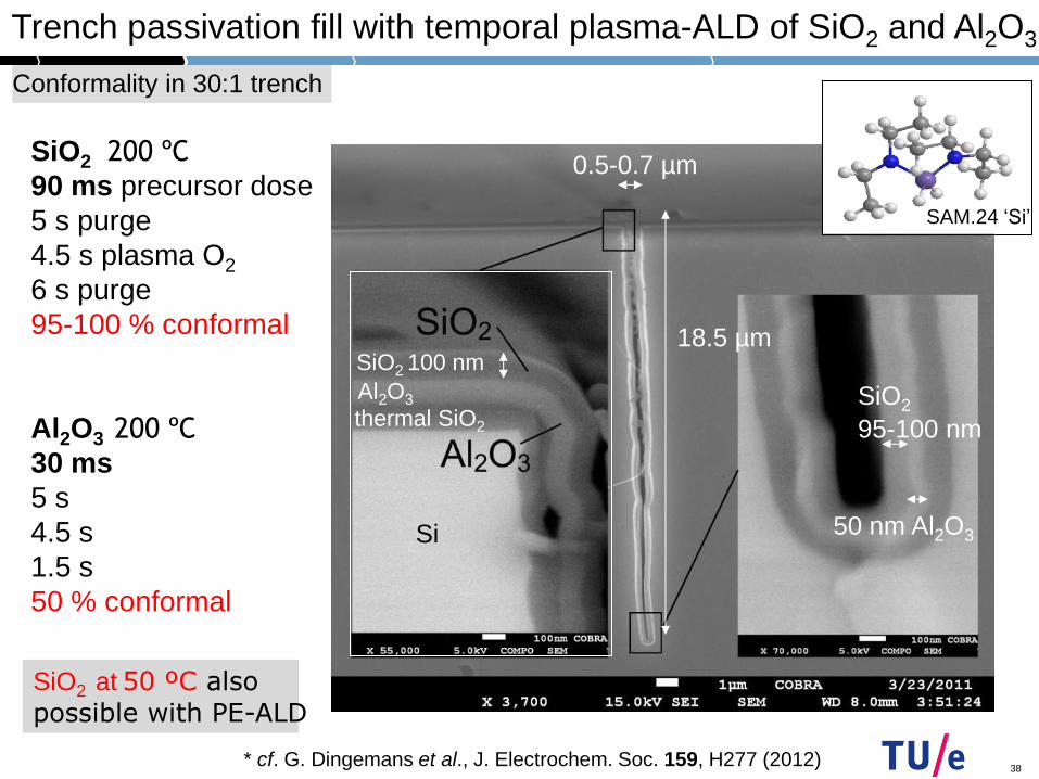
38
SiO2 200 ºC
90 ms precursor dose
5 s purge
4.5 s plasma O2
6 s purge
95-100 % conformal
Al2O3 200 ºC
30 ms
5 s
4.5 s
1.5 s
50 % conformal
Conformality in 30:1 trench
Trench passivation fill with temporal plasma-ALD of SiO2 and Al2O3
0.5-0.7 µm
18.5 µm SiO2 100 nm
thermal SiO2
Al2O3
Si 50 nm Al2O3
SiO2 95-100 nm
* cf. G. Dingemans et al., J. Electrochem. Soc. 159, H277 (2012)
‘Si’ SAM.24
SiO2 at 50 ºC also
possible with PE-ALD
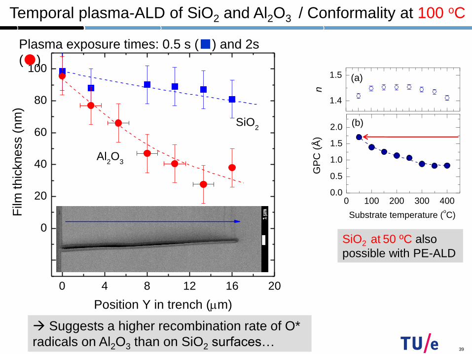
Temporal plasma-ALD of SiO2 and Al2O3 / Conformality at 100 oC
0 4 8 12 16 20
-20
0
20
40
60
80
100
Film
th
ickn
ess (
nm
)
Position Y in trench (m)
SiO2
Al2O
3
Plasma exposure times: 0.5 s (■) and 2s
(●)
Suggests a higher recombination rate of O*
radicals on Al2O3 than on SiO2 surfaces… 39
0 100 200 300 4000.0
0.5
1.0
1.5
2.0
nG
PC
(Å
)
(b)
Substrate temperature (oC)
1.4
1.5
(a)
SiO2 at 50 ºC also
possible with PE-ALD
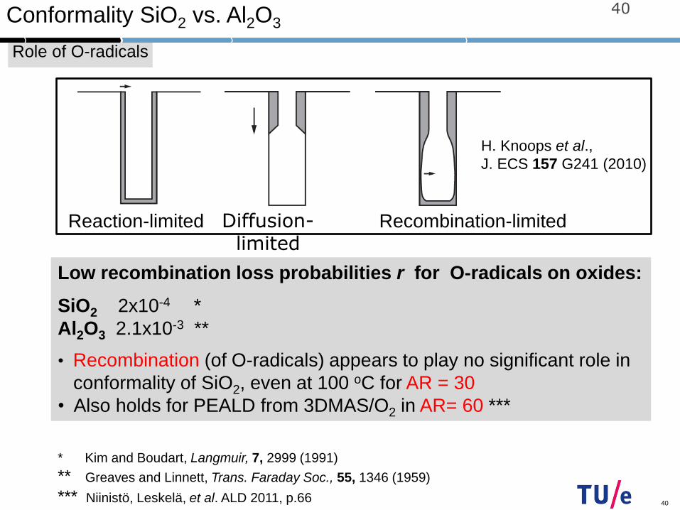
Role of O-radicals
40
Low recombination loss probabilities r for O-radicals on oxides:
SiO2 2x10⁻⁴ *
Al2O3 2.1x10⁻³ **
• Recombination (of O-radicals) appears to play no significant role in
conformality of SiO2, even at 100 oC for AR = 30
• Also holds for PEALD from 3DMAS/O2 in AR= 60 ***
Conformality SiO2 vs. Al2O3
* Kim and Boudart, Langmuir, 7, 2999 (1991)
** Greaves and Linnett, Trans. Faraday Soc., 55, 1346 (1959)
*** Niinistö, Leskelä, et al. ALD 2011, p.66
H. Knoops et al.,
J. ECS 157 G241 (2010)
Diffusion-limited
Reaction-limited Recombination-limited
40