thermally induced strain‐coupled highly stretchable and sensitive pyroelectric...
TRANSCRIPT

CO
MM
UN
ICATIO
N
© 2015 WILEY-VCH Verlag GmbH & Co. KGaA, Weinheim (1 of 6) 1500704wileyonlinelibrary.com
Thermally Induced Strain-Coupled Highly Stretchable and Sensitive Pyroelectric Nanogenerators
Ju-Hyuck Lee , Hanjun Ryu , Tae-Yun Kim , Sung-Soo Kwak , Hong-Joon Yoon , Tae-Ho Kim , Wanchul Seung , and Sang-Woo Kim *
J.-H. Lee, T.-Y. Kim, Prof. S.-W. Kim SKKU Advanced Institute of Nanotechnology (SAINT) Center for Human Interface Nanotechnology (HINT) Sungkyunkwan University (SKKU) Suwon 440-746 , Republic of Korea E-mail: [email protected] H. Ryu, S.-S. Kwak, H.-J. Yoon, T.-H. Kim, W. Seung, Prof. S.-W. Kim School of Advanced Materials Science and Engineering Sungkyunkwan University (SKKU) Suwon 440-746 , Republic of Korea
DOI: 10.1002/aenm.201500704
effect. [ 14,15 ] We utilized the different thermal expansion char-acteristics of neighbored two materials to build strain on fer-roelectric P(VDF-TrFE) fi lms to generate a piezoelectric effect using only thermal energy. [ 16 ] Therefore, the SPNG generates output power using the piezoelectric and pyroelectric effects on the P(VDF-TrFE) fi lm using thermal energy only. Our study is different PDMS, which does not have any piezoelectric or pyroelectric properties, also served as a template for presenting stretchability and applying compressive strain to P(VDF-TrFE) due to its very high thermal expansion when the SPNG is heated. It is a novel design for an energy harvesting system to enhance output performance and sensitivity using thermal energy. The highly sensitive SPNG operates from an extremely low temperature change (Δ T ≈ 0.64 K) to changes in high tem-perature (Δ T ≈ 18.5 K) and the SPNG provides highly robust and stable performance under stretching conditions.
Figure 1 a shows a schematic image of the thermally induced strain-coupled SPNG. The SPNG is mainly composed of three parts. Micropatterned P(VDF-TrFE) is a piezoelectric, pyro-electric active material [ 7,14 ] and micropatterned PDMS is not only suitable as a stretchable substrate template, [ 17 ] but also for applying strain to neighboring P(VDF-TrFE) using heat due to its very high thermal expansion coeffi cient (thermal expansion coeffi cient of PDMS: 310 × 10 −6 K −1 , [ 18 ] thermal expansion coeffi -cient of P(VDF-TrFE): 122 × 10 −6 K −1 [ 19 ] ). Lastly, a thin silver (Ag) fi lm and Ag nanowires (AgNWs) were introduced for a stretch-able top electrode (Figure S1 in the Supporting Information shows all fabrication processes in detail). The β-phase formation of P(VDF-TrFE) was confi rmed by X-ray diffraction (XRD) and Fourier transform infrared (FT-IR) spectroscopy (see Figure S2 in the Supporting Information). [ 20,21 ] The micropatterned P(VDF-TrFE) (width: 500 µm and height: 7 µm) and the pat-terned PDMS (width: 200 µm and height: 200 µm) can be viewed using an optical microscopy (OM) image and cross-sectional view of a fi eld emission-scanning electron microscope (FE-SEM) image (Figure 1 b) (Figure S3, Supporting Information shows full dimensions of the SPNG). Figure 1 c presents a photo image of the SPNG. In order to investigate the high sensitivity of the SPNG even when the temperature changes ever so slightly, we compared the SPNG with a normal PNG (NPNG) which is based on the fl at P(VDF-TrFE) coated onto a fl at and rigid Ni/SiO 2 /Si substrate. Figure 1 d,e shows the generated output voltages under the various rates of temperature change with the SPNG and the NPNG. When the temperature increases from room tempera-ture (RT), negative output voltage peaks are obtained.
When they are exposed to heat, a pyroelectric potential is generated across the thickness of P(VDF-TrFE). This generated pyroelectric potential drives carriers from the electrodes to the
Converting wasted energy into electrical energy has received great attention and become an important research fi eld, espe-cially since the commercialization of wearable device sys-tems, wireless sensors, and small electronics with low power consumption. [ 1–3 ] Wasted energy, such as mechanical energy, thermal energy, and photovoltaic energy, is accessible in eve-ryday life and very useful. Among them, thermal energy has always existed around us, especially in the human body which has always had temperature gradients and fl uctuations. Har-vesting energy from the huge amount of wasted thermal energy in our environments would be a great opportunity and very important for low power consumption electronics. [ 4–6 ]
Fluctuations in thermal energy, which can generate pyro-electric energy, exist everywhere due to wind, sun light, other various heat, and cooling sources. Pyroelectricity depends highly on the change of spontaneous polarization which results in charges separation. As a result, pyroelectric is a competi-tive method to harvest energy using wasted thermal energy. [ 7,8 ] Energy harvesters based on triboelectric, piezoelectric, ther-moelectric, and photovoltaic effects have already been actively researched and showed signifi cant results. [ 9–13 ] However, there is still a lack of research on energy harvesting based on the pyroelectric effect. In addition, the reported power-generating performance of pyroelectric nanogenerators (NGs) is relatively low compared with other energy harvesters such as piezoelec-tric or triboelectric NGs. [ 9,10,12 ] Therefore, enhancement of the pyroelectric performance is one of the signifi cant technical issues for meaningful usage of pyroelectric NGs as a new energy harvesting device.
In this paper, we report on how we have innovatively designed a stretchable pyroelectric NG (SPNG) based on a coupling of piezoelectric and pyroelectric effects using micropatterned poly(vinylidenefl uoride- co -trifl uoroethylene) [P(VDF-TrFE)] and micropatterned polydimethyl-siloxane (PDMS). The origin of coupling effect does not come from secondary pyroelectric
Adv. Energy Mater. 2015, 5, 1500704
www.MaterialsViews.comwww.advenergymat.de

CO
MM
UN
ICATI
ON
© 2015 WILEY-VCH Verlag GmbH & Co. KGaA, Weinheim1500704 (2 of 6) wileyonlinelibrary.com
external circuit; the output voltage and output current are meas-ured from the SPNG and the NPNG devices upon application of various temperature change rates. With exposure of the devices to temperature changes that range from low (Δ T ≈ 0.64 K) to high (Δ T ≈ 18.5 K), the output voltage of the SPNG range from around 8 mV to 2.48 V and output voltage of the NPNG range from around 2 mV to 0.54 V. The SPNG shows a clear enhance-ment of output performance readings that area about 4–5 times higher than those of the NPNG. As the output performance is proportionated to Δ T and d T /dt, we could achieve signifi cant enhancement using a thermally induced piezoelectric coupling effect. The operating mechanisms of the SPNG and the NPNG are discussed in Figure S4, Supporting Information.
According to piezoelectric and the pyroelectric theories, the output performance of NG depends on a change in spon-taneous polarization. [ 22,23 ] Our previous report expressed a change in spontaneous polarization as [ 7 ]
+ijΔ = ⋅ ⋅ ΔP d X p T (1)
where d is the piezoelectric coeffi cient, X is the applied stress, p is the pyroelectric coeffi cient, and Δ T is the change of tempera-ture. The application of heat results in applied stress in P(VDF-TrFE) in the SPNG which can be expressed as
,
( )( ) ( ) ( ) ,
( ) , ( ) ,
ε εα α
= ⋅ − ⋅= ⋅ − ⋅ ⋅ Δ
− − −
− −
X E EE E T
P VDF TrFE P VDF TrFE th P VDF TrFE PDMS th PDMS
P VDF TrFE L P VDF TrFE PDMS L PDMS (2)
where E is the Young’s modulus, ε th is the strain from thermal expansion, and α L is the linear expansion coeffi cient. Therefore, when the SPNG is heated, the change in spontaneous polariza-tion can be expressed as
= ( ) +31 ( ) , ( ) ,P d E E T p TP VDF TrFE L P VDF TrFE PDMS L PDMSα αΔ ⋅ ⋅ − ⋅ ⋅ Δ ⋅ Δ− − (3)
Based on the above equation, we have calculated the strain, stress, piezoelectric potential distribution of P(VDF-TrFE), and
temperature distribution of P(VDF-TrFE) under heat from 300 to 315 K using COMSOL multiphysics simulation software ( Figure 2 ). We have designed four devices, the fl at P(VDF-TrFE) on an SiO 2 /Si substrate, the patterned P(VDF-TrFE) on an SiO 2 /Si substrate, the fl at P(VDF-TrFE) on a PDMS substrate, and the patterned P(VDF-TrFE) on a patterned PDMS substrate, to verify micropatterning and substrate effects.
First, the temperature distributions of P(VDF-TrFE) on each device are simulated under the same heating condition as a function of time (Figure 2 a and Figure S5, Supporting Infor-mation). The average temperature in micropatterned P(VDF-TrFE) on the SiO 2 /Si substrate is higher than that of the fl at P(VDF-TrFE) on the SiO 2 /Si substrate under the same heat condition due to a high surface area from the micropatterned structure. The average temperature in the P(VDF-TrFE) on the PDMS substrate is higher than that of the P(VDF-TrFE) on the SiO 2 /Si substrate because of different thermal conductivity (thermal conductivity of P(VDF-TrFE) is 0.21 W m −1 K −1 , [ 24 ] PDMS is 0.15 W m −1 K −1 , [ 18 ] Si is 149 W m −1 K −1 , [ 25 ] and SiO 2 is 1.5 W m −1 K −1 [ 25 ] ). Heat remains in P(VDF-TrFE) rather than the PDMS substrate in the P(VDF-TrFE)/PDMS structure because of the low thermal conductivity of substrate. On the other hand, heat is immediately released through the SiO 2 /Si substrate in the P(VDF-TrFE)/SiO 2 /Si structure due to the high thermal conductivity of substrate. Therefore, the average tem-perature of the P(VDF-TrFE) on the PDMS substrate is higher than that of the P(VDF-TrFE) on the SiO 2 /Si substrate.
Based on the temperature distribution of each device, we also simulate thermally induced stress, strain, and the piezoelectric potential in Figure 2 b–e and Figure S6 (Supporting Informa-tion). The micropatterned P(VDF-TrFE) on the micropatterned PDMS substrate structure (Figure 2 e) shows higher piezoelec-tric potential compared to the fl at P(VDF-TrFE) on the PDMS substrate (Figure 2 d) even though it has a similar temperature distribution. The enhanced piezoelectric potential in micropat-terned P(VDF-TrFE) is derived from compressive strain, which
Adv. Energy Mater. 2015, 5, 1500704
www.MaterialsViews.comwww.advenergymat.de
Figure 1. a) Schematic image of the SPNG. b) Top-view OM image of the SPNG. The inset reveals a cross-sectional FE-SEM image of the SPNG. c) Photo image of the SPNG. d) Changes in temperature of NG and corresponding differential curves. e) Measured output voltages of the SPNG and NPNG under the differential rates of temperature change. The inset shows structure of the SPNG and NPNG.

CO
MM
UN
ICATIO
N
© 2015 WILEY-VCH Verlag GmbH & Co. KGaA, Weinheim (3 of 6) 1500704wileyonlinelibrary.com
is caused by neighboring micropatterned PDMS expansion due to an extremely high thermal expansion coeffi cient of PDMS (thermal expansion coeffi cient of PDMS is 310 × 10 −6 K −1 , [ 18 ] P(VDF-TrFE) is 122 × 10 −6 K −1 [ 19 ] ). Based on the piezoelectric and pyroelectric theory of P(VDF-TrFE), tensile strain in the x -axis generates positive piezoelectric potential, compressive strain in the x -axis generates negative piezoelectric potential and heat generates negative pyroelectric potential in P(VDF-TrFE). [ 7 ] Compressive strain is applied to the patterned P(VDF-TrFE) on the PDMS device and this generates a larger nega-tive piezoelectric potential, which enhances the total potential by coupling with the pyroelectric potential (detailed stress and strain distribution is given in the Supporting Information). Each device was also designed and manufactured to confi rm the simulation results (see Figure S7 in the Supporting Infor-mation). Output performances from all the devices showed similar behavior to the simulation results under heating conditions (Δ T ≈ 9.49 K, d T /dt ≈ 4.04 K s −1 ) (see Figure S8, Supporting Information).
In this study, we designed micropatterned structures not only for coupling of piezoelectric and pyroelectric effects, but also for enhancing the stretchability of the PNGs. In order to confi rm the stretchability of the SPNG, we have measured the pyroelectric output performance and resistance change of the top electrode with a different stretching rate ( Figure 3 a,b). There is no variation in the output voltage up to 15% of applied strain, and the SPNG demonstrated an almost stable output potential about 1.2 V at Δ T ≈ 50 K. The resistance of the top electrode is also extremely stable in up to 15% of the stretched condition. [ 26 ] To understand this behavior, we simulated the strain distribution of the device before and after the 15% stretched condition using COMSOL multiphysics simulation. Figure 3 c,d shows an x -direction strain distribution at the initial state of the device and an x -direction strain distribution at the 15% stretched condition, respectively. Interestingly, the tensile strain is more localized in patterned PDMS rather than P(VDF-TrFE) due to Young’s modulus difference between PDMS and P(VDF-TrFE) (Young’s modulus of P(VDF-TrFE) is 3 GPa, [ 27 ]
PDMS is 0.36 GPa [ 18 ] ). Also, the OM image of the SPNG con-fi rms that only PDMS is expanded rather than P(VDF-TrFE) after stretching. Figure 3 e shows the original state of the SPNG as we manufactured it with a 200 and 500 µm width of PDMS and P(VDF-TrFE), respectively. It was found that only PDMS expanded to around 230 µm and P(VDF-TrFE) was almost same as the initial condition of the 500 µm width when the SPNG was stretched to around 15% (Figure 3 f). These results indicate that the fabrication of highly stretchable and sensitive SPNGs without any performance degradation even under the contin-uous stretching mode is attributed to the mechanical durability of the patterned PDMS and top electrode, AgNWs. Thermally induced strain distributions of the SPNG at the initial state and 15% stretched condition were also simulated (see Figure S9 in the Supporting Information). Both simulation results show that the strain distribution inside P(VDF-TrFE) is almost the same.
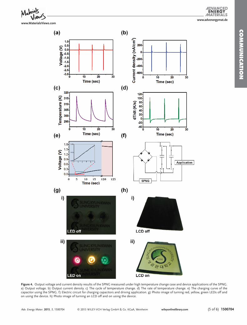
To utilize the SPNG for various applications, it is necessary to signifi cantly improve its power-generating performance. We have demonstrated the high output performance of the SPNG when the temperature increases from RT to 317 K (Δ T ≈ 22 K and d T /dt ≈ 105 K s −1 ), the SPNG generates around 2.5 V of output voltage and 570 nA cm −2 of output current density ( Figure 4 a–d). The charging feature of the capacitor via a recti-fi er is shown in Figure 4 e. The voltage of the capacitor reached 1.7 V at 120 s. In order to operate some electronic devices, we designed an integrated charging−discharging circuit for prac-tical applications comprised of the SPNG, a rectifying bridge (1N4148), a switch module, and two capacitors (3.3 µF). Two capacitors were connected in parallel so that they could be charged by the SPNG, while they were connected in series so that they could be discharged (Figure 4 f). When periodic thermal energy is applied to the SPNG, the total generating power from the SPNG is suffi cient to simultaneously operate all three red, yellow, and green light-emitting diodes (LEDs) (Figure 4 g). Moreover, a black liquid crystal display (LCD) screen with the Sungkyunkwan University logo is activated when the charged two capacitors by the SPNG are discharged (Figure 4 h).
Adv. Energy Mater. 2015, 5, 1500704
www.MaterialsViews.comwww.advenergymat.de
Figure 2. Simulation analysis of the devices by COMSOL multiphysics software under heat conditions. a) Temperature distributions of P(VDF-TrFE) on each device under the same heating condition as a function of time. b) Piezoelectric potential distribution of the fl at P(VDF-TrFE) on an Ni/SiO 2 /Si substrate. c) Piezoelectric potential distribution of the patterned P(VDF-TrFE) on an Ni/SiO 2 /Si substrate. d) Piezoelectric potential distribution of the fl at P(VDF-TrFE) on a PDMS substrate. e) Piezoelectric potential distribution of the patterned P(VDF-TrFE) on a PDMS substrate.

CO
MM
UN
ICATI
ON
© 2015 WILEY-VCH Verlag GmbH & Co. KGaA, Weinheim1500704 (4 of 6) wileyonlinelibrary.com
In summary, we have developed thermally induced strain-coupled highly stretchable and sensitive PNGs based on micropatterned P(VDF-TrFE), micropatterned PDMS, and a stretchable Ag/AgNWs electrode. We have successfully dem-onstrated the dramatic enhancement of the SPNG’s power-generating performance based on the coupling of piezoelectric and pyroelectric effects using different thermal expansion coef-fi cients and micropatterned architectures. We found that the highly sensitive SPNG operates from temperature changes that range from extremely low to high, and generates around 2.5 V
of output voltage and 570 nA cm −2 of output current density. This paper has discussed in detail the working mechanism of the SPNGs in terms of their polarization and thermal expan-sion. Thermally induced stress, strain, and piezoelectric poten-tial in the P(VDF-TrFE) of the SPNG were simulated in order to support the experimental results. Furthermore, we showed that the micropatterned structure of the SPNG is much more ben-efi cial at securing its high stretchability, fl exibility, mechanical durability, and robustness. The results obtained in this work strongly suggest that the SPNG could be applied in various
Adv. Energy Mater. 2015, 5, 1500704
www.MaterialsViews.comwww.advenergymat.de
Figure 3. a) Output voltage with a lateral stretch ratio of between 0% and 15%. b) The change in resistance of the top electrode with a lateral stretching ratio of between 0% and 20%. c) x -direction mechanical expansion strain distribution simulated by COMSOL multiphysics software in the initial state. d) x -direction mechanical expansion strain distribution simulated by COMSOL multiphysics software at 15% stretched condition. e) OM image of the SPNG surface in the initial condition. f) OM image of the SPNG surface after 15% stretching.
CO
MM
UN
ICATIO
N
© 2015 WILEY-VCH Verlag GmbH & Co. KGaA, Weinheim (5 of 6) 1500704wileyonlinelibrary.comAdv. Energy Mater. 2015, 5, 1500704
www.MaterialsViews.comwww.advenergymat.de
Figure 4. Output voltage and current density results of the SPNG measured under high temperature change case and device applications of the SPNG. a) Output voltage. b) Output current density. c) The cycle of temperature change. d) The rate of temperature change. e) The charging curve of the capacitor using the SPNG. f) Electric circuit for charging capacitors and driving application. g) Photo image of turning red, yellow, green LEDs off and on using the device. h) Photo image of turning an LCD off and on using the device.

CO
MM
UN
ICATI
ON
© 2015 WILEY-VCH Verlag GmbH & Co. KGaA, Weinheim1500704 (6 of 6) wileyonlinelibrary.com Adv. Energy Mater. 2015, 5, 1500704
www.MaterialsViews.comwww.advenergymat.de
kinds of promising device applications such as self-powered wearable electronics and e-skin applications.
Supporting Information Supporting Information is available from the Wiley Online Library or from the author.
Acknowledgements J.-H.L. and H.R. contributed equally to this work. This work was fi nancially supported by the Basic Science Research Program (Grant Nos. 2015R1A2A1A05001851 and 2009-0083540) through the National Research Foundation (NRF) of Korea Grant funded by the Ministry of Science, ICT and Future Planning.
Received: April 9, 2015 Revised: May 30, 2015
Published online: June 30, 2015
[1] J. A. Paradiso , T. Starnerd , IEEE Pervasive Comput. 2005 , 4 , 18 . [2] S. Xu , Y. Qin , C. Xu , Y. G. Wei , R. Yang , Z. L. Wang , Nat. Nano-
technol. 2010 , 5 , 367 . [3] Y. F. Hu , Y. Zhang , C. Xu , L. Lin , R. L. Snyder , Z. L. Wang , Nano Lett.
2011 , 11 , 2572 . [4] M. Zebarjadi , K. Esfarjani , M. S. Dresselhaus , Z. F. Ren , G. Chen ,
Energy Environ. Sci. 2012 , 5 , 5147 . [5] D. Liang , H. Yand , S. W. Finefrock , Y. Wu , Nano Lett. 2012 , 12 , 2140 . [6] H. Liangbing , M. Pasta , F. L. Mantia , L. Cui , S. Jeong ,
H. D. Deshazer , J. W. Choi , S. M. Han , Y. Cui , Nano Lett. 2010 , 10 , 708 .
[7] J.-H. Lee , K. Y. Lee , M. K. Gupta , T. Y. Kim , D.-Y. Lee , J. Oh , C. Ryu , W. J. Yoo , C.-Y. Kang , S.-J. Yoon , J.-B. Yoo , S.-W. Kim , Adv. Mater. 2014 , 26 , 765 .
[8] D. Zabek , J. Taylor , E. L. Boulbar , C. R. Bowen , Adv. Energy Mater. 2015 , 5 , 1401891 .
[9] K. Y. Lee , J. Chun , J.-H. Lee , K. N. Kim , N.-R. Kang , J.-Y. Kim , M. H. Kim , K.-S. Shin , M. K. Gupta , J. M. Baik , S.-W. Kim , Adv. Mater. 2014 , 29 , 5037 .
[10] K. Y. Lee , D. K , J.-H. Lee , T. Y. Kim , M. K. Gupta , S.-W. Kim , Adv. Funct. Mater. 2014 , 24 , 37 .
[11] R. Venkatasubramanian , E. Siivola , T. Colpitts , B. O’Quinn , Nature 2011 , 403 , 597 .
[12] Y. Yang , J. H. Jung , B. K. Yun , F. Zhang , K. C. Pradel , W. Guo , Z. L. Wang , Adv. Mater. 2012 , 24 , 5357 .
[13] K.-S. Shin , T. Y. Kim , G. C. Yoon , M. K. Gupta , S. K. Kim , W. Seung , H. Kim , S. Kim , S.-W. Kim , Adv. Mater. 2014 , 26 , 5619 .
[14] C. R. Bowen , J. Taylor , E. LeBoulbar , D. Zabek , A. Chauhan , R. Vaish , Energy Environ. Sci. 2014 , 7 , 3836 .
[15] H. H. S. Chang , R. W. Whatmore , Z. Huang , J. Appl. Phys. 2009 , 106 , 114101 .
[16] H. Kawai , Jpn. J. Appl. Phys. 1969 , 8 , 975 . [17] Zhixin Wang , Graduate Thesis and Dissertation , University of South
Florida , South Florida , 2011 . [18] D. E. Gray , American Institute of Physics Handbook , McGraw-Hill ,
New York 1957 . [19] W.-K. Jeung , S.-M. Choi , Y.-J. Kim , J. Electr. Eng. Technol. 2006 , 1 , 263 . [20] R. A. Whiter , V. Naratan , S. Kar-Narayan , Adv. Energy Mater. 2014 , 4 ,
1400519 . [21] K. Koga , N. Nakano , T. Hattori , H. Ohigashi , J. Appl. Phys. 1990 , 67 ,
965 . [22] B. Ploss , B. Ploss , F. G. Shin , H. L. W. Chan , C. L. Choy , IEEE Trans.
Dielectrics Electrical Insul. 2000 , 7 , 517 . [23] Z. L. Wang , Nano Res. 2008 , 1 , 1 . [24] Y. W. Wong , N. M. Hui , E. L. Ong , H. L. W. Chan , C. L. Choy , J. Appl.
Polymer Sci. 2003 , 89 , 3160 . [25] H. Tada , A. E. Kumpel , R. E. Lathrop , J. B. Slanina , P. Nieva ,
P. Zavracky , I. N. Miaoulis , P. Y. Wong , J. Appl. Phys. 2000 , 87 , 4189 . [26] M. S. Miller , J. C. O’Kane , A. Niec , R. S. Carmichael ,
T. B. Carmicahel , ACS Appl. Mater. Interfaces 2013 , 5 , 10165 . [27] J. M. Park , J. W. Kong , D. S. Kim , D. J. Yoon , Compos. Sci. Technol.
2005 , 65 , 241 .