chapter 6. custom integrated circuits
TRANSCRIPT

Chapter 6. Custom Integrated Circuits
Chapter 6. Custom Integrated Circuits
Academic and Research Staff
Professor Jonathan Allen, Professor John L. Wyatt, Jr., Professor Srinivas Devadas, Professor Jacob White
Visiting Scientists and Research Affiliates
James H. Kukula1
Graduate Students
Robert C. Armstrong, Donald G. Baltus, Cyrus S. Bamji, Curtis S. Chen, Steven J. Decker, Ibrahim M.Elfadel, Marina Frants, Juha M. Hakkarainen, Craig L. Keast, Songmin Kim, Kevin Lam, Steven B. Leeb,Jennifer A. Lloyd, Andrew Lumsdaine, Ignacio S. McQuirk, Keith S. Nabors, Joel Phillips, Khalid Rahmat,Mark W. Reichelt, Mark N. Seidel, Amelia H. Shen, Luis M. Silveira, David L. Standley, RicardoTelichevesky, Christopher B. Umminger, Filip Van Aelten, Woodward Yang, Paul C. Yu
Technical and Support Staff
Dorothy A. Fleischer, Susan E. Nelson
6.1 Custom Integrated Circuits
Sponsors
Analog Devices, Inc.IBM Corporation
Project Staff
Professor Jonathan Allen, Robert C. Armstrong,Donald G. Baltus, Cyrus S. Bamji, Mark W.Reichelt, Filip Van Aelten
The overall goal of VLSI CAD research is toprovide the means to produce custom integratedcircuits correctly, quickly, and economically. Tra-ditionally, correctness is checked at several repres-entational levels, such as layout (via design rulechecking), and circuit and logic (both via simu-lation). The techniques for checking correctnessare usually local to the particular representationallevel involved. While these techniques are impor-tant components of the design testing, they do notattempt to provide alignment and consistencychecks between the different representationallevels and an input behavioral specification. Inaddition, they do not characterize the set of pos-sible designs at each representational level corre-sponding to the initial functional specificationwhile ranging over a variety of performance levels.For this reason, there is an increasing need toprovide CAD tools that can serve as the framework
for design exploration, providing the desired per-formance together with consistently aligned rep-resentations at all levels.
In this research group, we are studying a variety ofresearch topics with an emphasis on performance-directed synthesis of custom VLSI designs. Anoverview of the viewpoint that motivates theseprojects has recently been provided in a majorsurvey paper2 in which the need for coordinatingthe design optimization process over the severallevels of representation is emphasized. Sincedesign exploration is so central to the productionof high-performance designs, emphasis is placedon how performance can be characterized at theseveral levels of representation and how overalloptimal performance can be achieved in an inte-grated way. In addition to the basic issues ofcircuit optimization, architectures for digital signalprocessing have been studied because of thehighly parallel nature of the algorithms involvedand the need for a very high level of real-time per-formance in these systems. We have increased ouremphasis on developing the means for formallyspecifying designs that facilitate performance-directed design exploration as well as efficient ver-ification of correctness of the coordinated set ofdesign-level representations. All of these studiesare taking on an increasingly theoretical approach,signifying the transition of digital system designfrom an art to a science.
1 IBM Corporation.
2 J. Allen, "Performance-Directed Synthesis of VLSI Systems," Proc. IEEE 78(2): 336-355 (1990).
265

Chapter 6. Custom Integrated Circuits
In previous work, techniques were developed toautomatically transfer a netlist of an MOS circuit(either NMOS or CMOS in any circuit style) to ahighly efficient, compacted layout. Providingalgorithmic control over this important transforma-tion is essential in overall design optimization.This procedure has been used as a "back end" fortechnology mapping processes, and the corre-sponding program has been very successful inbenchmark tests.3
Given this assurance of the generation of high-quality layout for circuit netlist specification, atten-tion is now being turned to performanceexploration at the architectural level, with a focuson digital signal processing applications which arehighly parallel. In this research, architectures thatrepeatedly use a small set of circuit cells in aregular array are being emphasized, such assystolic arrays. While these arrays, which utilizenearest neighbor communication, have been suc-cessfully used for a wide variety of signal pro-cessing tasks, it is of interest to explore morerelaxed models where communication is allowedto extend beyond nearest neighbors to a largerlocal area. This extension admits a wider class ofarchitectures and invites a more comprehensivelevel of design exploration where architecturalflexibility is traded off against more complex, localdelay models. Formal techniques for specifyingthese signal processing tasks at a behavioral levelhave been introduced, and means for mapping thealgorithm onto multiple index spaces have beendevised, together with the means to explore thesemappings. An affine delay model has been intro-duced to quantify communication delay, and anoverall integer linear programming approach hasbeen used to optimize the overall design on atiming performance basis. In addition, branch andbound techniques have been used to prune thepossibly large search space to a smaller and moremanageable set of alternatives that can be quicklyassessed. In this way, global optimization is beingdirectly addressed through the linking of architec-tural exploration and delay models in the contextof a large but restricted design space. Since thesecircuit models are well characterized, the previ-ously developed techniques for automatic conver-
sion between circuit netlist representation andlayout provides an overall means for simultaneousoptimization across all representational levels, fromlayout through circuit, to logic, and architecture.This investigation aims to provide one of the firstinstances of overall global optimization across allrepresentational levels, avoiding premature localoptimization at any single level of representation.
There is increasing interest in extending circuitdesign and optimization techniques to the devicelevel by refining the device models, and also bysimulating them directly rather than using approxi-mate average device model parameters in a circuitsimulator. While the device-level equations can besolved directly to provide the needed accuracy,their solution is generally found to be too time-consuming on conventional architectures. Accord-ingly, Reichelt has been studying techniques forthe parallelization of transient two-dimensionalsimulation of MOS devices using waveform relaxa-tion techniques.4 Uniform convergence of thewaveform relaxation algorithm in this applicationhas been demonstrated, and speedups betweenfive and eleven times have been found using thesenew algorithms. These techniques have recentlybeen implemented on three-dimensional parallelarchitectures in a way that exploits the inherentparallelism of the waveform relaxation techniques.
In earlier work, Bamji demonstrated how context-free grammars could be used to formally representlarge classes of circuit netlists, such as ratioedNMOS designs, static CMOS designs, andprecharge/evaluate circuit designs. 5 He alsorepresented the class of all layouts as a regularstructure grammar and showed how to verify thecorrectness of the resulting layout using parsingtechniques. This formalism has essentially pro-vided a new technique for hierarchical design ruleverification using a cell library through formalcharacterization of the interactions of cell tem-plates.6 Design rule verification is achieved by cov-ering the layout with these templates, which aredefined in terms of graphs, and all operations areperformed in the graph domain. The verificationprocedure is incremental, and because the numberof cell instances is usually much smaller than thenumber of mask geometries, it is much faster than
3 D.G. Baltus and J. Allen, "SOLO: A Generator of Efficient Layouts from Optimized MOS Circuit Schematics," Pro-ceedings of the 25th Design Automation Conference, June 1988.
4 M. Reichelt, J. White, and J. Allen, "Waveform Relaxation for Transient Two-Dimensional Simulation of MOSDevices," IEEE Trans. Comput-Aided Des., forthcoming.
5 C.S. Bamji and J. Allen, "GRASP: A Grammar-based Schematic Parser," Proceedings of the 26th Design Auto-mation Conference, June 1989.
6 C.S. Bamji and J. Allen, "GLOVE: A Graphic-based Layout Verifier," forthcoming.
266 RLE Progress Report Number 133

Chapter 6. Custom Integrated Circuits
techniques that directly manipulate mask geom-etries. A current emphasis is on the automatic dis-covery of cells from nonhierarchical layout.Through these means we expect to derive designhierarchy automatically, and hence, suggest newcells for a library. The graph-based template tech-niques are similar to those previously used in aregular structure generator,7 which has proved tobe a convenient method for the elaboration oflayout corresponding to higher level architecturalconnectivity.
In earlier studies, Van Aelten showed how toperform the verification of circuit properties basedon a grammar-based schematic parser developedby Bamji. These formal techniques are now beingextended to the verification of relations betweensynchronous machines. Since the machines maybe implemented in many different ways, it isimportant to be able to transform representationsof these machines into alternate forms that can bedirectly compared. Using a new set of primitiverelations between string functions, an arbitrarilylong sequence of behavioral transformations canbe compressed into a single, composite relationthat is guaranteed to correctly represent the givensequence of primitive transformations. 8 In this way,it is possible to use these composite transforma-tions to verify the behavioral specification againstthe resultant logic implementation with oneautomata equivalence check, using any one ofseveral available methods. In this way, a compu-tationally expensive verification technique isreduced to a much simpler verification task.
We continue to focus on issues of design databaseand framework specification. It is increasinglyrecognized that a design database is the centralcomponent of an overall design system, along witha variety of specialized CAD algorithms that utilizeone consistently maintained overall design repre-sentation. Nevertheless, maintenance of this data-base so that all levels of representational view areconsistent with one another and are henceprojections of one (and only one) underlyingdesign is an exceedingly difficult problem. Onesingle representational formalization has recentlybeen introduced by Armstrong, and it is expectedto support all levels of representation currently uti-lized or anticipated. 9 By setting up a series of
explicit correspondences between representationallevels, consistency can readily be verified andmaintained in the face of design modifications atany of the several different representational levels.This automatic consistency maintenance is highlydesirable in any design system, and can be readilycoupled to performance exploration strategies atlevels where a change at a higher level ofabstraction gives rise to many possible lower levelrepresentations, as in the transition from a circuitspecification to layout. A preliminary version ofthis procedure has now been implemented, and isbeing tested over a substantial variety of cases.
With the advent of a new emphasis on centraldatabases and their connections to specializedCAD algorithms, there is new concern for thestudy of integrated, cooperative CAD computingenvironments involving both workstations andmainframes. A proposal has been developed forthe study of coordinated workstation, mainframe,and large disk system environments that are inter-connected in a flexible way using fiberopticswitching. In this way, large, high-performancedisk systems are flexibly coupled between bothmainframe servers and high-performance work-stations, and a means is provided to explore theoptimal distribution of tasks over such a distrib-uted framework. This environment also provides astructure in which distributed parallel algorithmscan run in a coherent way within an overall envi-ronment that supports other specialized nonparallelCAD algorithms.
6.2 The MIT Vision ChipProject: Analog VLSI Systemsfor Fast Image Acquisition andEarly Vision Processing
Sponsors
National Science Foundation/Defense AdvancedResearch Projects AgencyGrant MIP 88-14612
Project Staff
Professor John L. Wyatt, Jr., Professor BertholdK.P. Horn, Professor Hae-Seung Lee, Professor
7 C.S. Bamji, C.E. Hanck, and J. Allen, "A Design-by-Example Regular Structure Generator," Proceedings of the22nd Design Automation Conference, June 1985, pp. 16-22.
8 F. Van Aelten, J. Allen, and S. Devadas, "Verification of Relations between Synchronous Machines," 1991 MCNCLogic Synthesis Workshop, forthcoming.
9 R.C. Armstrong, A Formal Approach to Incremental Consistency Maintenance in Multirepresentation VLSI Data-bases, Ph.D. diss. proposal, Dept. of Electr. Eng. and Comput. Sci., MIT, 1987.
267
Chapter 6. Custom Integrated Circuits
Tomaso Poggio, Professor Charles G. Sodini, Pro-fessor Jacob White, Steven J. Decker, Ibrahim M.Elfadel, Juha M. Hakkarainen, Craig L. Keast,Ignacio S. McQuirk, Mark N. Seidel, David L.Standley, Christopher B. Umminger, WoodwardYang, Paul C. Yu
6.2.1 Introduction
In real-time machine vision, the sheer volume ofimage data to be acquired, managed and proc-essed leads to communications bottlenecksbetween imagers, memory, and processors andalso to very high computational demands. Ourgroup is designing experimental analog/VLSIsystems to overcome these problems. The work ispresently concentrated entirely on early visiontasks, i.e., tasks that occur early in the signal flowpath of a machine vision system. Designs of chipsfor certain tasks in velocity estimation, imagemoment calculations, depth from stereo, and edgedetection are currently underway or have beencompleted.
This project began in September 1988, and thefaculty involved are Professors Berthold K.P. Hae-Seung Lee, Tomaso Poggio, Charles G. Sodini,Jacob White, and John L. Wyatt, Jr., who is theprincipal investigator. This work was inspired byProfessor Carver Mead's pioneering efforts at theCalifornia Institute of Techology, although ourproject methods and goals are different fromMead's.
The goal of this project is to design and build pro-totype early vision systems that are remarkablylow-power, small, and fast. The typical systemwill perform one or more computation-intensiveimage-processing tasks at hundreds to thousandsof frames per second using only tens to hundredsof milliwatts. The entire system with lens, imager,power supply and support circuitry could fit insidea cigar box.
In this project, we are exploring the various typesof analog processing for early vision. There is nosingle design strategy, but each design has manyof the following features:
* sensors and processing circuitry integrated ona single chip,
* parallel computation,
* analog circuits for high speed, small area andlow power,
* selection of tasks and algorithms requiring lowto moderate precision (roughly equivalent to
6-8 bit fixed point precision in a digitalmachine),
* special emphasis on computations that mapnaturally to physical processes in silicon, e.g.,to relaxation processes or to resistive grids,
* emphasis on charge-domain processing, e.g.,CCD and switched-capacitor implementations,for maximal layout density and compatibilitywith CCD sensors,
* sufficiently fast processing that no long-termstorage circuitry is required, and
* careful matching of algorithms, architecture,circuitry and (often custom) fabrication formaximum performance.
The advantages of this analog design approach toearly vision hardware are (1) high speed (both inthe sense of high throughput and low latency),(2) low power, and (3) small size and weight.High throughput can be important in high speedinspection processes, e.g., for printed materials orPC boards. Low latency is very important forclosed loop systems because delays are destabi-lizing. Relevant examples might include vehiclenavigation and robot arm guidance. Low powertogether with small size and weight are importantfor airborne and space applications. And finally,small systems tend to be affordable.
These advantages are achieved at a cost. Oneproblem is that a high degree of care and expertiseis required for high performance analog design.Another is that performance and functionality ofanalog integrated circuits is critically dependent onexact fabrication process parameters. For thesereasons, the first design of an analog chip, even byan experienced designer, often does not work, sothat repeated efforts are required.
Another problem is that there is a large amount oflabor and frequent delays involved in custom fabri-cation on campus. Finally, analog systems havelittle flexibility compared with their digital counter-parts. Thus analog design, often coupled withcustom fabrication, is only appropriate whenextremely high performance is required.
Chips are fabricated through MOSIS wheneverpossible. Chips requiring special processing arefabricated on campus at MIT's MicrosystemsTechnology Laboratories where Craig Keast andProfessor Charles Sodini have developed a specialCMOS/CCD fabrication process for vision applica-tions.
Sections 1.1.2 and 1.1.3 describe chips that havebeen designed and tested by doctoral studentsDavid Standley and Woodward Yang.
268 RLE Progress Report Number 133

Chapter 6. Custom Integrated Circuits
y
axis of leastinertia
centroid
0. > x
object
Figure 1. Example of object centroid and axis of leastinertia.
6.2.2 Fast Imager and ProcessorChip for Object Position andOrientation
This analog VLSI chip finds the position and ori-entation of an object's image against a dark back-ground. The algorithm is based on finding the firstand second moments of the object intensity.These moments allow the centroid (an indicator ofposition) and the axis of least inertia (an indicatorof orientation) to be computed; see figure 1. IfI(x,y) is the intensity as a function of position, andwe (initially) assume that I(x, y) = 0 outside theobject, then the required quantities are given by
SIl(x, y)h(x, y)dA
for all of the following h:
h(x, y) = 1, x, y, xy, x2 - Y2
(X2 and y2 are not needed separately). All of theweighting functions h are harmonic; i.e., theLaplacian vanishes identically:
Ah(x, y) - 0.
This observation is a key to a scheme proposed byHorn, in which an analog computer based on aresistive sheet (or resistor grid) can be con-structed, in principle. In the implementationdescribed here, an N x N array of discrete intensitydata is reduced to a set of 4N quantities by a 2-Dresistor grid and is subsequently reduced to a setof just eight quantities by 1-D resistor lines, all ina continuous-time, asynchronous fashion - noclocking required. The eight outputs can be
digitized, and the centroid and orientation can befound using simple expressions. While resistivesheets have been used in earlier systems tocompute position, none have been previously usedto perform the orientation task, which requirescomputing second moments.Figure 2 shows the resistor grid and its associatedarray of photoreceptor cells, which are uniformlyspaced and occupy most of the chip area. Theobject image is focused onto the surface of thechip, inside the array. Each photoreceptor cellcontains a phototransistor and processing circuitry;it converts the incident light intensity into acurrent that is injected into the grid. Thresholdingis available to remove a dim (yet nonzero) scenebackground, so it does not interfere with the cal-culation. If the intensity I at a particular cell isbelow an adjustable threshold value Ith, then nocurrent is injected. If I > Ith, then the outputcurrent, which is analogous to the gray-levelweighting at that location, is proportional to I - Ith*The result is a continuous, piecewise-linearresponse characteristic. The array size is 29 x 29;intentional image blurring over a few elementsgives substantially increased resolution.
The perimeter of the grid is held at a constantvoltage by the current buffers in figure 2; thisensures proper operation of the grid as a "datareduction" computer. The buffer outputs aresimply copies of the currents flowing into themfrom the grid; the buffers are needed to isolate thegrid from the effects of other circuitry. Figure 3,which shows the complete architecture of thechip, indicates how the (copied) grid currents arefed into resistor lines on the perimeter, how theends of these lines are connected, and where theeight output currents exit the chip near thecorners. These currents are measured by externalcircuitry (which also holds the ends of the lines atground potential). In this setup, there are twolines on each side: one uniform and one quadraticline. These calculate weighted sums of the gridcurrents, where the weighting is (respectively) alinear or square-law function of the position alongthe line. The buffer outputs are steered either tothe uniform or quadratic lines, so that four outputsare available at a time; i.e., multiplexing is requiredhere (but is not necessary in general).
Working chips have been fabricated using theMOSIS service. The die size is 7.9 mm x 9.2 mm,and the imaging array is a 5.5 mm square. Accu-racy is dependent on the object. For moderatelysized and sufficiently elongated objects, e.g. adiamond of diagonal dimensions 25 by 50 on a(normalized) 100 by 100 image field, orientation istypically determined to within +2. The speed is5000 frames per second, and power consumptionis typically 30 mW.
269

Chapter 6. Custom Integrated Circuits
Figure 2. Resistor grid and photoreceptor cell array.
6.2.3 Integrated CCD Imager andProcessors for Edge Detection
Parallel, Pipelined Architecture
Many image processing algorithms and machinevision tasks consist of calculations or operationsperformed on spatially localized neighborhoods.Therefore, the highly parallel nature of these algo-rithms can be effectively exploited if they are per-formed directly on the imaging device before theparallel structure of the data is disrupted by serialdata output.
For a typical CCD imaging array, the parallel, pipe-lined architecture (see figure 4) provides a balanceof computation speed, internal clock rate, internalstorage, and I/O bandwidth without degrading theimager fill-factor (sensitivity). As columns ofimage data are clocked from left to right in parallel,local interactions between neighboring columnelements are directly computed by the processorelements. As row values are sequentially clockedthrough the processor, local interactions betweenneighboring row elements are similarly performedby utilizing delay elements. This architecture isable to efficiently implement linear convolutionsthat are separable and recursively defined. Thisarchitecture is also suitable for certain types ofnonlinear filtering operations that perform imagesegmentation, a basic machine vision task.
Figure 3. Main chip architecture.
CCD Processors for Edge Detection
A full fill-factor CCD (64 x 64) imager with anintegrated, analog CCD signal processor for edgedetection was implemented using standard 4 um,CCD/NMOS technology. By combining simplecharge-domain, analog circuitry in a parallel, pipe-lined architecture, the prototype image processorwas capable of performing a simple edge detectionalgorithm at 1000 frames/second. Furthermore,this signal processing capability was achieved withonly a 15% increase in area, without any additionalfabrication steps, decreasing the fill-factor of theCCD imager, or a significant increase in power dis-sipation.
While there are many edge detection algorithms,the LoG (Laplacian of Gaussian) of the image waschosen for its ease of implementation. TheLaplacian is a rotationally symmetric, scalar oper-ator. The zero-crossings of the Laplacian corre-spond to maxima in the image gradient which areinterpreted as object edges. The Gaussian acts asa low-pass image filter that reduces the effects ofnoise in the image and has several desirable prop-erties such as (1) rotational symmetry, (2)separability into 1-D convolutions within row andcolumn elements, and (3) approximation by abinomial distribution which is recursively defined.The Gaussian (actually, binomial) convolver onthis chip is a parallel, pipelined version of a CCDarchitecture developed first by Sage and Lattes atMIT Lincoln Laboratories.
In addition to image sensing, CCDs are alsocapable of performing simple analog charge-domain computations such as charge packet split-
270 RLE Progress Report Number 133
photoreceptor cell
Chapter 6. Custom Integrated Circuits
PARALLL. PIPELINED ARCHITECTURE
dat storage processing elements
-E3-- -Er- D_delay element
--c-
Figure 4. The parallel, pipelined architecture for highthroughput image processing. The entire image istransferred through the column and row processors as apipelined sequence of column vectors of image pixels.The column processors compute local interactionsbetween neighboring column pixels in parallel. Therow processors pipeline the computation of local inter-actions between neighboring row pixels by using addi-tional delay elements.
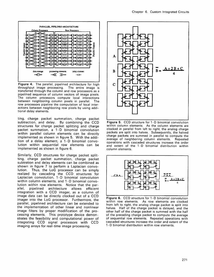
ting, charge packet summation, charge packetsubtraction, and delay. By combining the CCDstructures for charge packet splitting and chargepacket summation, a 1 -D binomial convolutionwithin parallel column elements can be directlyimplemented as shown in figure 5. With the addi-tion of a delay element, a 1-D binomial convo-lution within sequential row elements can beimplemented as shown in figure 6.
Similarly, CCD structures for charge packet split-ting, charge packet summation, charge packetsubtration and delay elements can be combined asshown in figure 7 to perform a Laplacian convo-lution. Thus, the LoG processor can be simplyrealized by cascading the CCD structures forLaplacian convolution, 1-D binomial convolutionwithin column elements, and 1-D binomial convo-lution within row elements. Notice that the par-allel, pipelined architecture allows efficientintegration with a CCD imager, as a column ofimage data can be directly clocked out of a CCDimager into the LoG processor. Furthermore, theparallel, pipelined architecture can be extended tothe implementation of other linear and nonlinearimage filters by proper modification of the pro-cessing elements. This prototype device demon-strates the feasibility and computational power ofintegrating CCD signal processors with CCDimaging arrays for real-time image processing.
Figure 5. CCD structure for 1-D binomial convolutionwithin column elements. As the column elements areclocked in parallel from left to right, the analog chargepackets are split into halves. Subsequently, the halvedcharge packets are summed in parallel to compute theaverage of neighboring column elements. Repeatedoperations with cascaded structures increase the orderand extent of the 1-D binomial distribution withincolumn elements.
SB- A +2B+C4
Figure 6. CCD structure for 1-D binomial convolutionwithin row elements. As row elements are clockedfrom left to right, the analog charge packet is split intohalves. Half of the charge packet is delayed, and theother half of the charge packet is summed with the halfof the preceding charge packet to compute the averageof sequential row elements. Repeated operations withcascaded structures increase the order and extent of the1-D binomial distribution within row elements.
271
"= A+2B+C4

Chapter 6. Custom Integrated Circuits
Figure 7. CCD structure for Laplacian convolution.As image data are clocked from left to right, the chargepackets are split, delayed, summed, and subtracted tocompute the discrete convolution approximating theLaplacian computation.
6.2.4 Overall Project Scope
Listed below are the individual efforts that areunderway or have been completed in this project.The single-chip systems are chips with imagers forinput that produce highly processed, low-bandwidth output that can be readily handled byconventional digital systems. David Standley'schip in section 1.1.3. is an example. The "modularvision system component chips" may or may nothave imagers on board. They produce high band-width output such as filtered images or depthmaps that require specialized processing hardwarefor high speed operation.
Single-Chip Systems
CMOS Image Moment Chip (completed)CCD/CMOS Focus of Expansion Chipgress)
(in pro-
Modular Vision System Component Chips
CCD/CMOS Analog Convolver (completed)CCD/CMOS Image Smoothing and Segmentation
Chip (in progress)CCD/CMOS Stereo Chip (in progress)Switched-Capacitor Surface Reconstruction
Chip (in progress)
Technology Development
CCD/CMOS Fabrication Process (completed)Switched-Capacitor Resistive Grids (completed)
.. A3. A2, A....
.. , B 2, B1....
C3 , C2, Ci....
272 RLE Progress Report Number 133
SA2+- B z-4B +B1+
CMOS Image Segmentation Circuits (in progress)
Theory
Stability of Active Resistive-Grid Systems(completed)
Texture and Halftoning Using Markov RandomFields (in progress)
Switched-Capacitor Network Settling Time(in progress)
Least-Squares Camera Calibration Method(in progress)
Simulation
Parallel Simulator for Large Arrays of AnalogCells (in progress)
Publications
Elfadel, I., and R. Picard. "Miscibility MatricesExplain the Behavior of Grayscale TexturesGenerated by Gibbs Random Fields." SPIE Pro-ceedings on Intelligent Robots and ComputerVision IX, OE/Boston '90, Boston, Massachu-setts, November 4-9, 1990.
Keast, C.L., and C.G. Sodini. "A CCD/CMOSProcess for Integrated Image Acquisition andEarly Vision Signal Processing." ProceedingsSPIE Charge-Coupled Devices and Solid StateSensors, Santa Clara, California, February 1990,pp. 152-161.
Lumsdaine, A., J.L. Wyatt, Jr., and I.M. Elfadel."Nonlinear Analog Networks for ImageSmoothing and Segmentation." J. VLSI Sig.Process. Forthcoming.
Lumsdaine, A., J. Wyatt, and I. Elfadel. "NonlinearAnalog Networks for Image Smoothing andSegmentation." Proceedings of the IEEE Inter-national Symposium on Circuits and Systems,New Orleans, Louisiana, May 1990, pp.987-991.
Sarpeshkar, R., J.L. Wyatt, Jr., N.C. Lu, and P.D.Gerber, "Mismatch Sensitivity of a Simultane-ously Latched CMOS Sense Amplifier." IEEE J.Solid-State Circuits. Forthcoming.
Standley, D. "Stability in a Class of Resistive GridNetworks Containing Active Device Realiza-tions of Nonlinear Resistors." Proceedings ofthe IEEE International Symposium on Circuitsand Systems, New Orleans, Louisiana, May1990, pp. 1474-1477.

Chapter 6. Custom Integrated Circuits
Umminger, C.B., and C.G. Sodini. "SwitchedCapacitor Networks for Monolithic Image Pro-cessing Systems." Submitted to IEEE J. Solid-State Circuits.
Wyatt, J.L., Jr., and M. Ilic. "Time-Domain Reac-tive Power Concepts for Nonlinear,Nonsinusoidal or Nonperiodic Networks." Pro-ceedings of the IEEE International Symposiumon Circuits and Systems, New Orleans,Louisiana, May 1990, pp. 387-390.
Wyatt, J., D. Standley, and B. Horn. "Local Com-putation of Useful Global Quantities UsingLinear Resistive-Grid Networks." Postersession, Conference on Neural Networks forComputing, Snowbird, Utah, April, 1990.
Yang, W., and A.M. Chiang. "A Full Fill-FactorCCD Imager with Integrated SignalProcessors." Proceedings of the ISSCC, SanFrancisco, California, February 1990, pp.218-219.
Patents
Decker, S., H.-S. Lee, and J.L. Wyatt, Jr."Resistive Fuse Circuits for Image Segmenta-tion and Smoothing." Submitted to U.S. PatentOffice 12/14/90, receipt no. 628-340.
Standley, D., and B.K.P. Horn. "Analog VLSI Chipfor Object Position and Orientation." Submittedto U.S. Patent Office 9/28/90, receipt no.591,145.
Theses
Umminger, C.B. Switched Capacitor Networks forMachine Vision. S.M. thesis. Department ofElectrical Eng. and Comput. Sci. MIT, 1990.
Yang, W. The Architecture and Design of CCDProcessors for Computer Vision. Ph.D. diss.Dept. of Electr. Eng. and Comput. Sci. MIT,1990.
6.3 Techniques for LogicSynthesis, Verification andTesting
Sponsors
Analog Devices Career DevelopmentAssistant Professorship
U.S. Navy - Office of Naval ResearchContract N0014-87- K-0825
Project Staff
Professor Srinivas Devadas, James H. Kukula,Curtis S. Chen, Marina Frants, Kevin Lam, AmeliaH. Shen, Filip Van Aelten
6.3.1 IntroductionIn order to design and build large-scale computersthat achieve and sustain high performance, it isessential to carefully consider reliability issues.Although these issues have several aspects, ourfocus here is on the important problem ofdetecting failures in a computer's VLSI compo-nents which are caused by errors in the designspecification, implementation or manufacturingprocesses.
Design verification involves ensuring that thespecification of a design is correct prior to carryingout its implementation. Implementation verifica-tion ensures that the manual design or automaticsynthesis process is correct, i.e., checking that themask-level descriptions obtained correctly imple-ment the specification. Manufacture testinginvolves checking the complex fabrication processfor correctness, i.e., checking that there are nomanufacturing defects on the integrated circuit. Itshould be noted that the three verificationmechanisms described above deal not only withverifying the functionality of the integrated circuitbut also with its performance.
In the Custom Integrated Circuits Group at MIT,we are attempting to develop synthesis, specifica-tion and verification mechanisms that are versatileas well as efficient. More importantly, we aredeveloping strategies that address reliability issuesin the many steps of the complex VLSI designprocess, and this involves varied levels of designabstraction from behavioral specifications to mask-level layout. Because many aspects of reliabilitycannot be investigated by focusing on a singlelevel of design abstraction, such a completeprogram is essential when addressing reliability.
In the following sections, we elaborate on ourcurrent work in developing CAD algorithms andtools for highly reliable VLSI circuits and on ourplans for the future. Included in the description isour research in the development of provablycorrect behavioral transformations with applica-tions to design and implementation verification,synthesis of testable VLSI circuits in the area ofmanufacture test, and the development of a frame-work for logic synthesis, verification and testing.
In Sections 6.3.2 through 6.3.4, we describe workcategorized largely by the mathematical and algo-rithmic techniques used in each problem domain.
273

Chapter 6. Custom Integrated Circuits
6.3.2 Design Verification
Introduction
The specifications for a large VLSI circuit are typi-cally expressed in a high-level language by a com-puter architect or VLSI designer. Then thearchitect uses high-level simulators to checkwhether the exact functionality of the circuit hasbeen captured in the design. Unfortunately, anexhaustive simulation that can guarantee correct-ness is possible only for the smallest circuits.Ideally, the architect would like to formally verifyand guarantee that the specifications are correct,so that, if they are implemented and fabricatedwithout error, a functionally-correct IC will result.
Several errors may occur in the manual process ofdesign specification. For example, in a recent per-sonal computer (PC) product by a major company,a particular number which was supposed to besquared was multipled by two instead. This wastracked to an error in the specification. The spec-ification had been rigorously (but obviously notexhaustively) simulated. Protocol chips are typi-cally small compared to general-purpose yprocessors, but experience has shown that they areparticularly prone to deadlock errors, due to incor-rect specifications.
While we believe that formal verification methodswill never replace simulation, they can augmentsimulation-based correctness checking in designverification. Verification methods could uncoverspecification errors without simulating hugenumbers of test cases or using exorbitant amountsof CPU time. We have recently begun work in thearea of design verification, specifically in the areasof temporal-logic-based model checking and pro-tocol verification.
Temporal Logic Model Checking
Model checking, a design verification methoddeveloped initially by Clarke et al. at CMU, 1' (1)specifies a property that the design should satisfyas a formula in computation-tree logic (CTL) and(2) verifies a design specification against the CTLformula using a model checker.
The model checking approach suffers from severaldrawbacks. First, the designer has to specify man-
ually the properties that the specification is sup-posed to satisfy. This can become a tedious anderror-prone task for complex properties and largedesigns. Second, not all useful properties can bespecified in CTL. More expressive logics havebeen devised, but the complexity of modelchecking increases for such logics. Third, modelchecking entails the traversal of the entire statespace of the design specification, which can behuge. The last mentioned problem is called stateexplosion.
We have developed strategies to efficiently traversethe state space of a given design specification (orimplementation) using a mixed depth-first/breadth-first strategy (c.f. "Sequential LogicVerification" on page 276) as opposed to previoustraversal algorithms." This traversal method ismore complex to implement than the traversalmethods proposed in the past, and modelchecking under this approach requires substantialmodifications to retain efficiency. We will developa new model checking algorithm based on ourtraversal algorithm. We believe that this new algo-rithm will be applicable to larger circuits than pre-vious approaches have been.
Protocol Verification by SymbolicAnalysis
One problem with most current approaches todesign verification is that they do not scale wellwith problem size. For instance, model checkingusing currently available traversal algorithms for an8-bit circuit will typically take significantly moretime than for a 4-bit version of the same circuit,even though the property to be checked for isindependent of bit-width.
Symbolic analysis can alleviate the scalabilityproblem. For instance, checking a protocol corre-sponding to interdependent processes and inter-acting sets of timers for correctness involveschecking to ensure that deadlock does not occur.More simply stated, control does not remain indef-initely in a particular loop. One way we cananalyze the loop is to traverse the entire statespace represented by the loop, but this approachhas the same drawbacks mentioned above. Asymbolic analysis can result in a significantly fasterjudgment regarding the nature of the loop. The
10 E.M. Clarke and 0. Grumberg, "Research on AutomaticComput. Sci. 2: 269-290 (1987).
Verification of Finite State Concurrent Systems," Ann. Rev.
11 A. Ghosh, S. Devadas, and A.R. Newton, "Verification of Interacting Sequential Circuits," paper presented at the27th Design Automation Conference, Orlando, Florida, June 1990, pp. 213-219.
274 RLE Progress Report Number 133

Chapter 6. Custom Integrated Circuits
existence or non-existence of exit conditions canbe determined easily.
We are attempting to classify protocols based ontheir amenability to symbolic analysis. We havefound that the state space corresponding to loopsin a common class of protocols can be simplyspecified using a linear system of equations. Thisimplies that the reachability analysis of such proto-cols can be accomplished in polynomial time. Atraversal method that depends on the bit-widthcould take exponential time for these circuits. Weare currently trying to generalize our method tohandle a larger class of protocols.
6.3.3 Implementation Verification
Introduction
During the design process, increasingly sophisti-cated optimization tools that modify a design toimprove its area, performance or power dissipationcharacteristics are applied simultaneously or insequence at various levels of design abstractions.Beginning from a behavioral specification, we typi-cally move through register-transfer level repres-entations, symbolic finite state machinerepresentations, logic-level representations andtransistor-level representations all the way tomask-level layout.
In order to ensure a working IC, each step of thedesign process above has to be checked for cor-rectness. A viewpoint might be that we can checkthe transformations applied by the CAD tools forcorrectness once, and all the designs produced bythe CAD system will be "correct by construction."Verifying the correctness of transformations in asynthesis system is absolutely necessary, but ourexperience has found that it is equally essential toprovide an independent verification mechanism.For example, in logic synthesis systems all logicoptimization steps are typically verified, formally orinformally, to be correct, but experience has shownthat it is necessary to supply post facto verificationprocedures to independently verify the results ofthe application of logic transformations on a par-ticular example. Similarly, while behavioral trans-formations may have been proved correct, thecorrectness of their realization in a particular soft-ware system is not presently amenable to proof,and, as a result, the final product of their applica-tion in synthesizing a circuit also requires inde-pendent verification.
Timing Verification
It is important to determine efficiently and accu-rately the critical path delay of a VLSI circuit sothat the clock period can be chosen to be greaterthan the critical delay. Overestimating the criticalpath can lead to an unnecessarily slow design,while underestimating the critical path has dan-gerous reliability implications.
Determining the critical path of a combinationalcircuit is complicated because a combinationalcircuit may have false paths, i.e., paths that arenever sensitized during normal system operation.Therefore, simply picking the longest path in thecircuit as the critical path can result in gross over-estimations of critical delay.
Viability has been proposed by McGeer andBrayton as a robust and correct criterion for deter-mining the critical path delay of a combinationalcircuit. Currently, algorithms that determine thelongest viable path in a circuit require largeamounts of CPU time on medium-large circuits.We are investigating more efficient means of deter-mining the longest viable path in a given network.In particular, we see a connection between deter-mining the longest viable path and generating atest for a particular multiple stuck-at fault in thecircuit.
Circuit-Level Verification
Logic net-lists can be implemented in a variety ofcircuit-level methodologies. Static or dynamic cir-cuits in CMOS or nMOS may be used. In the caseof dynamic circuits, a wide range of clockingmethodologies serve as design alternatives. Dif-ferent methodologies impose differing sets ofrestrictions on the topology and interconnection ofthe circuit blocks. Violations of these circuitdesign rules can go undetected during simulation.It is important that one checks for schematic-levelcorrectness under the chosen design methodology.
Recent work by Bamji and Allen12 formalized theprocess of verifying that a circuit-level schematicobeys a particular design methodology. Circuitcorrectness was tied to a rigorous set of context-free grammar composition rules. These rulesdefine how a small set of module symbols may becombined for circuits adhering to the design meth-odology. Schematic net-lists are represented bygraphs, and composition rules are defined as graph
12 C. Bamji and J. Allen, "GRASP: A Grammar-Based Schematic Parser," in Proceedings of the 26th Design Auto-mation Conference, June 1990, pp. 448-453.
275

Chapter 6. Custom Integrated Circuits
transformations similar to grammatical productions.Starting with a circuit net-list, a hierarchical parsetree that can demonstrate the well-formedness ofthe circuit is constructed. Since the procedure ishierarchical and incremental, it operates one ortwo orders of magnitude faster than previousapproaches.
A drawback to the above approach is that it canhandle only circuit design methodologies whichcan be specified under context-free grammar rules.While context-free grammars can be used tospecify a variety of circuit design methodologies(e.g., a 2-phase CMOS clocking methodology),complex special-case rules typically cannot bespecified. We are currently investigating the use ofhigher-level grammars under a similar mechanismwhich will allow for the verification of morecomplex circuit design methodologies.
Sequential Logic Verification
It is necessary to verify the equivalence of combi-national or sequential circuits described at thelogic level to check that a logic design step or alogic optimization system has not introduced errorsinto the design.
Recently, there has been considerable progress inthe area of sequential logic verification. Twobroad classes of approaches can be identified -approaches that use reduced, ordered Binary Deci-sion Diagrams as their base representation toperform a breadth-first traversal of the State Tran-sition Graph (STG) of a FSM 13 and approachesthat use cube representations to perform a depth-first traversal of the STG. 14 The former approachperforms significantly better than the latter ondatapath-like FSMs whose STGs are highly con-nected, while the latter outperforms the former oncounter-like FSMs where there are long chains ofstates.
We have developed a depth-first traversal tech-nique for sequential machines that enables the
traversal of counter FSMs in O(n) steps, where nis the number of bits in the counter. Our depth-first geometric chaining is based on it traversinggeometrically increasing (or decreasing) chains ofstates and edges in the STG in any given set ofsteps. Other STG traversal approaches require 2n
steps, since only one state can be traversed ineach step. We believe that a synergistic combina-tion of depth-first geometric chaining and previ-ously proposed breadth-first approaches offers anefficient traversal technique for a broad class ofcircuits that include both datapath and controlportions. We will implement and investigate theapplicability of this mixed depth-first/breadth-firststrategy on real-life circuits.
Behavioral Verification
As described above, equivalence checkingbetween two finite-state automata or two combi-national logic circuits is precisely defined and sup-ported by a body of theoretical work. The majorissue in the use of these algorithms is CPU effi-ciency. In contrast, verifying that a logic-leveldescription correctly implements a behavioralspecification is considerably less developed. Onemajor hindrance toward a precise notion of behav-ioral verification has been that parallel, serial orpipelined implementations of the same behavioraldescription can be implemented in finite-stateautomata with different input/output behaviors.15
In recent work,16 we used nondeterminism tomodel the degree of freedom that is afforded byparallelism in a behavioral description that alsocontains complex control. Given some assump-tions, we showed how the set of finite automataderivable from a behavioral description under allpossible schedules of operations can be repres-ented compactly as an input-programmedautomaton (p-Automaton). The above methodallows for extending the use of finite-stateautomata equivalence-checking algorithms to theproblem of behavioral verification.
13 0. Coudert, C. Berthet, and J.C. Madre, "Verification of Sequential Machines Using Boolean Functional Vectors,"In IMEC-IFIP International Workshop on Applied Formal Methods for Correct VLSI Design, November 1989, pp.111-128.
14 S. Devadas, H-K. T. Ma, and A.R. Newton, "On the Verification of Sequential Machines at Differing Levels ofAbstraction," in IEEE Trans. Comput.-Aided Des. 7: 713 (June 1988); A. Ghosh, S. Devadas, and A.R. Newton,"Verification of Interacting Sequential Circuits," paper presented at the 27th Design Automation Conference,Orlando, Florida, June 1990, pp. 213-219.
15 M.C. McFarland and A.C. Parker, "An Abstract Model of Behavior for Hardware Descriptions," in IEEE Trans.Comput. C-32:621 (1983).
16 S. Devadas and K. Keutzer, "An Automata-Theoretic Approach to Behavioral Equivalence," in Proceedings of theInternational Conference on Computer-Aided Design, November 1990.
276 RLE Progress Report Number 133

Chapter 6. Custom Integrated Circuits
We are in the process of extending the aboveapproach to handle a richer set of behavioral trans-formations including pipelining and complex don'tcare conditions specified at a behavioral level. Webelieve that the use of p-Automata represents ageneral method to verify behavior against imple-mentation.
6.3.4 Manufacture Test and VLSISynthesis for Testability
Introduction
Once a chip has been fabricated, it is essential tocheck that no manufacturing defects have beenintroduced during the fabrication process. Manu-facturing defects are modeled at different levels ofdesign abstraction, and these fault models are usedas a base for generating test vectors for a givendesign.
Fault models associated with defects that alterlogical functionality are called logical fault models.For example, the most commonly used and thesimplest logical fault model is the single stuck-atfault model, where a single wire in the IC is tied toa constant logical "1" or "0." Enhanced logicalfault models like the multiple stuck-at fault modeland the bridging fault model are more comprehen-sive, i.e., test vectors generated under these faultmodels typically detect a larger fraction of possiblemanufacturing defects. Deriving the test vectorsunder these fault models is considerably more dif-ficult. For instance, given k wires in a circuit, thereare only 2k single stuck-at faults, but 3 k - 1 mul-tiple stuck-at faults (multifaults), an astronomicalnumber even for small circuits. However, for someapplications reliability considerations are para-mount, and it may be necessary to obtain as com-prehensive a test set as possible.
Just checking the logical functionality of a fabri-cated circuit is not enough, its performance has tobe verified as well. Manufacturing defects candegrade performance without altering logicalfunctionality. Temporal or dynamic fault modelslike the gate delay fault model, transistor stuck-open fault model, and the path delay fault modelhave been proposed to model manufacturingdefects that alter the performance characteristics of
a circuit. As with the more comprehensive logicalfault models, test generation under these dynamicfault models is considerably more difficult thanunder the simplistic single stuck-at fault model.
Most circuits being designed today are not testablefor dynamic faults, and testing for multifaults andbridging faults requires exorbitant amounts of CPUtime. Also, post-design testability measurescannot, in general, increase the testability of thecircuit under these fault models. Our solution tothis problem is to completely integrate testabilityconsiderations into an automatic design process,i.e., synthesize the circuit to be highly or fullytestable under any given fault model.
VLSI circuits are typically sequential, and theproblem of generating tests for sequential circuitsis more difficult than that for combinational cir-cuits, under any given fault mooel. While tech-niques such as scan design can transform asequential test problem into a simpler one of com-binational test generation, these techniques havenot found widespread use due to reasons stem-ming from the design constraints, and the area andperformance penalties associated with scanmethods. Our research in testing also targets testgeneration under stuck-at and delay fault modelsfor non-scan VLSI circuits, and synthesis forsequential testability.
Combinational Logic Synthesis forTestability Under Enhanced FaultModels
Combinational logic synthesis and optimization isa well-understood problem. The traditional costfunctions used in synthesis have been layout areaand circuit performance. Researchers have onlyrecently begun to investigate the effect of logictransformations on the single and multiple stuck-atfault testability of a circuit 7 We are working onderiving algebraic and Boolean transformations forlogic circuits to improve testability (and removeredundancy) with minimal or no impact on areaand performance. Methods for implicit/test gener-ation, i.e., obtaining test vectors to detect stuck-atfaults as a by-product of the optimization steps,will be investigated. These methods are potentiallymuch more efficient than explicit test generationalgorithms, especially for multiple stuck-at faults.
17 G.D. Hachtel, R.M. Jacoby, K. Keutzer, and C.R. Morrison, "On the Relationship Between Area Optimization andMultifault Testability of Multilevel Logic," paper published in the International Conference on Computer-AidedDesign, November 1989, 422-425, (extended version submitted to IEEE Trans. Comput.-Aided Des.); S. Devadasand K. Keutzer, "Necessary and Sufficient Conditions for Robust Delay-Fault Testability of Logic Circuits," in theProceedings of the Sixth MIT Conference on Advanced Research on VLSI (Cambridge: MIT Press, 1990).
277

Chapter 6. Custom Integrated Circuits
Physical defects in ICs can degrade performancewithout affecting logic functionality. It is impor-tant to ensure that a given IC satisfies its timingspecifications - This requires performing a delayfault test. This is especially important for aggres-sive design methodologies that push processingtechnology to the utmost. We have done somerecent work on the synthesis of delay-fault testablecombinational circuits. Certain classes of large cir-cuits can be synthesized for complete robust path-delay-fault testability (which is the mostcomprehensive fault model devised thus far) withsmall area and performance penalties.' 8 Theprimary drawbacks of current techniques are thatnon-flattenable random logic circuits, those thatcannot be reduced to sum-of-products form,cannot be synthesized efficiently. We are currentlyimproving upon the available synthesis techniquesthrough the use of Binary Decision Diagrams asour base representation. Multiplexor-based net-works, derived from replacing the nodes of BinaryDecision Diagrams by 2-input multiplexors, havevery interesting testability properties. Exploitingthese properties can lead to an efficient synthesis-for-test strategy.
We are also investigating dynamic compactiontechniques for test sets during synthesis. Com-paction techniques tailored toward multiplestuck-at faults and delay faults are being devel-oped. For instance, we believe that complete mul-tiple stuck-at-fault test sets can be generated forrandom logic blocks that are only two to fourtimes the size of the single-fault test set. Nonro-bust delay test methodologies are not as compre-hensive as robust delay test methodologies butoffer scope for smaller test vector sets.
Sequential Logic Synthesis forTestability Under Enhanced FaultModels
VLSI circuits are typically sequential. A popularmethod of reducing the complexity of sequentialtest generation has involved the use of scan designmethodologies (e.g., LSSD). Sequential test gen-eration 19 and sequential logic synthesis for test-ability techniques that ensure non-scansingle-stuck-at fault testability20 have been, andwill continue to be, a subject of investigation atMIT and elsewhere.
We are now looking toward the synthesis ofsequential circuits for delay-fault testability. It iswell known that arbitrary vector pairs cannot beapplied to a sequential circuit under a standard-scan design methodology. This means that even ifthe combinational logic of a sequential circuit ismade fully robustly delay-fault testable, it may notbe fully testable under a standard-scan designimplementation. An enhanced scan flip-flop thatcan store two bits of state is required. This "triple-latch" flip-flop increases the area of the circuit.
We have made preliminary investigations into thesynthesis of non-scan sequential circuits for gate-delay-fault testability21 These initial approacheswere limited to circuits of small size. Severalavenues are being explored in current research.First, we are developing techniques that ensurefully robustly gate-delay-fault testable chips undera standard-scan design methodology. Second, weare exploring the use of partial enhanced-scan andstandard-scan design methods to improve therobust delay-fault testability of sequential circuits.Third, we are investigating the use of partialstandard-scan and non-scan design. Our goal isto eventually obtain non-scan circuits that arecompletely robustly gate-delay-fault testable, withnegligible area/performance penalties.
18 S. Devadas and K. Keutzer, "Design of Integrated Circuits Fully Testable for Delay Faults and Multifaults," In Pro-
ceedings of the International Test Conference, October 1990, pp. 284-293; S. Devadas and K. Keutzer, "Synthesis
and Optimization Procedures for Delay-Fault Testable Combinational Logic," paper presented at the 27th DesignAutomation Conference, Orlando, Florida, June 1990.
19 A. Ghosh, S. Devadas, and A. R. Newton, "Test Generation and Verification of Highly Sequential Circuits," In
Proceedings of the International Conference on Computer-Aided Design, November 1989, pp. 362-365.
20 S. Devadas and K. Keutzer, "A Unified Approach to the Synthesis of Fully Testable Sequential Machines," IEEE
Trans. Comput.-Aided Des., 10(1): 39-50 (1991); S. Devadas and H-K. T. Ma, "Easily Testable PLA-based Finite
State Machines," IEEE Trans. on Comput.-Aided Des., 9(5): 614-611 (1990).
21 S. Devadas," Delay Test Generation for Synchronous Sequential Circuits," in Proceedings of the International Test
Conference (Washington, D.C.: August 1989), pp. 144-152.
278 RLE Progress Report Number 133

Chapter 6. Custom Integrated Circuits
Publications
Ashar, P., S. Devadas, and A.R. Newton."Testability- Driven Decomposition of LargeFinite State Machines." Proceedings of Interna-tional Conference on Computer Design.: VLSI inComputers and Processors, Boston, Massachu-setts, September 1990.
Ashar, P., S. Devadas, and A.R. Newton."Optimum and Heuristic Algorithms for A For-mulation of Finite State Machine Decompos-ition." IEEE Trans. Comput.-Aided Des. 10(3):296-310 (1991).
Ashar, P., A. Ghosh, S. Devadas, and K. Keutzer."Implicit State Transition Graphs: Applicationsto Sequential Logic Synthesis and Test." Pro-ceedings of the International Conference onComputer-Aided Design, Santa Clara, Cali-fornia, November 1990.
Ashar, P., S. Devadas, and A. Ghosh. "BooleanSatisfiability and Equivalence Checking UsingGeneral Binary Decision Diagrams." Interna-tional Conference on Computer Design: VLSI inComputers and Processors, Cambridge, Mass-achusetts, October 1991.
Ashar, P., S. Devadas, and K. Keutzer. "TestabilityProperties of Multilevel Logic NetworksDerived From Binary Decision Diagrams." Pro-ceedings of the Conference on AdvancedResearch in VLSI, Santa Cruz, California, March1991.
Ashar, P., S. Devadas, and A.R. Newton."Irredundant Interacting Sequential MachinesVia Optimal Logic Synthesis." IEEE Trans.Comput.-Aided Des. 10(3): 311-325 (1991).
Bryan, M.J., S. Devadas, and K. Keutzer."Testability- Preserving CircuitTransformations." Proceedings of the Interna-tional Conference on Computer-Aided Design,Santa Clara, California, November 1990.
Bryan, M.J., S. Devadas, and K. Keutzer. "Analysisand Design of Regular Structures for RobustDynamic Fault Testability." IEEE InternationalSymposium on Circuits and Systems,Singapore, June 1991.
Bryan, M.J., S. Devadas, and K. Keutzer, "Analysisand Design of Regular Structures for RobustDynamic Fault Testability." Inter. J. Comput.-Aided VLSI Des. Forthcoming.
Cheng, K-T., S. Devadas, and K. Keutzer. "RobustDelay-Fault Test Generation and Synthesis for
Testability Under a Standard Scan Method-ology." 28th Design Automation Conference,San Francisco, California, June 1991.
Devadas, S. "Delay Test Generation forSychronous Sequential Circuits." Inter. J.Comput.-Aided VLSI Des. Forthcoming.
Devadas, S. "Optimization of Interacting FiniteState Machines Using Sequential Don't Cares."IEEE Trans. Comput.-Aided Des. Forthcoming.
Devadas, S. "Optimal Layout Via BooleanSatisfiability." Inter. J. Comput.-Aided VLSIDes. 2(2): 251-262 (1990).
Devadas, S. "Optimization of Interacting FiniteState Machines Using Sequential Don't Cares."IEEE Trans. Comput.-Aided Des. Forthcoming.
Devadas, S., and H-K. T. Ma. "Easily TestablePLA-based Finite State Machines." IEEE Trans.Comput.-Aided Des. 9(5): 614-611 (1990).
Devadas, S., and K. Keutzer. "A Unified Approachto the Synthesis of Fully Testable SequentialMachines." IEEE Trans. Comput.-Aided Des.10(1): 39-50 (1991).
Devadas, S., and K. Keutzer. "Synthesis of RobustDelay-Fault Testable Circuits: Practice." IEEETrans. Comput.-Aided Des. Forthcoming.
Devadas, S., and K. Keutzer. "Synthesis of RobustDelay-Fault Testable Circuits: Theory." IEEETrans. Comput.-Aided Des. Forthcoming.
Devadas, S., and K. Keutzer. "An Automata-Theoretic Approach to Behavioral Equivalence."Proceedings of the International Conference onComputer-Aided Design, Santa Clara, Cali-fornia, November 1990.
Devadas, S., K. Keutzer, and A. Ghosh. "RecentProgress in VLSI Synthesis for Testability." Pro-ceedings of the VLSI Test Symposium, AtlanticCity, April 1991.
Devadas, S., and K. Keutzer. "Design of IntegratedCircuits Fully Testable for Delay Faults andMultifaults." Proceedings of the InternationalTest Conference, Washington, D.C., September1990.
Devadas, S., and A.R. Newton. "Exact Algorithmsfor Output Encoding, State Assignment andFour-Level Boolean Minimization." IEEE Trans.Comput.-Aided Des. 10(1): 13-27 (1991).
Devadas, S., and K. Keutzer. "An Automata-Theoretic Approach to Behaviorial
279

Chapter 6. Custom Integrated Circuits
Equivalence." Intern. J. Comput.-Aided VLSIDes. Forthcoming.
Devadas, S., K. Keutzer, and J.K. White. "Esti-mation of Power Dissipation in CMOS Combi-national Circuits Using Boolean FunctionManipulation." IEEE Trans. Comput.-AidedDes. Forthcoming.
Devadas, S., K. Keutzer, and S. Malik. "ASynthesis-Based Approach to Test Generationand Compaction for Multifaults." 28th DesignAutomation Conference, San Francisco, Cali-fornia, June 1991.
Devadas, S., K. Keutzer, and A.S. Krishnakumar."Design Verification and Reachability AnalysisUsing Algebraic Manipulation." InternationalConference on Computer Design: VLSI in Com-puters and Processors, Cambridge, Massachu-setts, October 1991.
Ghosh, A., S. Devadas, and A.R. Newton."Heuristic Minimization of Boolean RelationsUsing Testing Techniques." Proceedings ofInternational Conference on Computer Design:VLSI in Computers and Processors, Boston,Massachusetts, September 1990.
Ghosh, A., and S. Devadas. "Implicit Depth-FirstTransversal of Sequential Machines." IEEEInternational Symposium on Circuits andSystems, Singapore, June 1991.
Ghosh, A., S. Devadas, and A.R. Newton. "TestGeneration and Verification of Highly Sequen-tial Circuits." IEEE Trans. Comput.-Aided Des.Forthcoming.
Ghosh, A., S. Devadas, and A.R. Newton. "Syn-thesis for Sequential Logic Testability usingRegister-Transfer Level Descriptions." Pro-ceedings of the International Test Conference,Washington, D.C., September 1990.
6.4 Mixed Circuit/DeviceSimulation
Sponsors
IBM CorporationU.S. Navy - Office of Naval Research
Contract N00014-87-K-0825
Project Staff
Mark W. Reichelt, Professor Jacob White, Pro-fessor Jonathan Allen
For critical applications, the four-terminal lumpedmodels for MOS devices used in programs likeSPICE are not sufficiently accurate. Also, it is dif-ficult to relate circuit performance to processchanges using lumped models. Sufficiently accu-rate transient simulations can be performed if,instead of using a lumped model for each tran-sistor, some of the transistor terminal currents andcharges are computed by numerically solving thedrift-diffusion based partial differential equationapproximation for electron transport in the device.However, simulating a circuit with even a few ofthe transistors treated by solving the drift-diffusionequations is very computationally expensivebecause the accurate solution of the transportequations of an MOS device requires a two-dimensional mesh with more than a thousandpoints.
One approach to accelerating this kind of mixeddevice and circuit simulation is to use waveformrelaxation to perform the transient simulation, notonly at the circuit level, but also inside the devicesbeing simulated with a drift-diffusion description.In the present investigation, the WR algorithm isbeing applied to the sparsely-connected system ofalgebraic and ordinary differential equations intime generated by standard spatial discretization ofthe drift-diffusion equations that describe MOSdevices. Several theoretical results about the uni-formity of WR convergence for the semiconductorproblem have been proved,22 and we have alsocompleted experiments using waveform relaxationto perform transient two-dimensional simulation ofMOS devices. Speed and accuracy comparisonsbetween standard direct methods and red/blackoverrelaxed waveform-relaxation -Newton indicatethat for the experiments examined, calculated ter-minal currents match well between the methods,and our overrelaxed waveform-relaxation-Newton
22 M. Reichelt, J. White, J. Allen and F. Odeh, "Waveform Relaxation Applied to Transient Device Simulation," Pro-ceedings of the International Symposium on Circuits and Systems, Espoo, Finland, June 1988, pp. 1647-1650.
280 RLE Progress Report Number 133

Chapter 6. Custom Integrated Circuits
method was five to eleven times faster.23 Currently,efforts are underway to develop the WORDSprogram (Waveform OverRelaxation Device Simu-lator) into a more robust code, with adaptive SORparameterization; Poisson-only, or one or twocarrier simulation options; and improved physicalmodeling. All physical models were verified bycomparison and agreement with the industry-standard device simulator PISCES. Finally, a par-allel version of WORDS was written for theiPSC/2 parallel architecture, demonstrating aspeedup factor of 15.5 on 16 processors.
6.5 Simulation Algorithms forClocked Analog Circuits
Sponsors
AT&TAnalog DevicesDigital Equipment CorporationIBM CorporationNational Science Foundation
Grant MIP 88-58764U.S. Navy - Office of Naval Research
Contract N00014-87-K-0825
Project Staff
Steven B. Leeb, Luis M. Silveira, Professor JacobWhite
A challenging problem in the area of analog cir-cuits is the simulation of clocked analog circuitslike switching filters, switching power supplies,and phase-locked loops. These circuits are com-putationally expensive to simulate using conven-tional techniques because these kinds of circuitsare all clocked at a frequency whose period isorders of magnitude smaller than the time intervalof interest to the designer. To construct such along time solution, a program like SPICE orASTAP must calculate the behavior of the circuitfor many high frequency clock cycles. The basicapproach to simulating these circuits more effi-ciently is to exploit only the property that thebehavior of such a circuit in a given high fre-quency clock cycle is similar, but not identical to,
the behavior in the preceding and followingcycles. Therefore, by accurately computing thesolution over a few selected cycles, an accuratelong time solution can be constructed.
Simulating clocked analog systems is an oldproblem, but this novel approach has led to a veryefficient algorithm for the distortion analysis ofswitched-capacitor filters. The idea is based onsimulating selected cycles of the high-frequencyclock accurately with a standard discretizationmethod and pasting together the selected cyclesby computing the low frequency behavior with atruncated Fourier series. If carefully constructed,the nonlinear system that must be solved for theFourier coefficients is almost linear and can besolved rapidly with Newton's method.24 Transientbehavior, important for switching power supplydesigners, has also been accelerated using similartechniques.25 In particular, the "envelope" of thehigh-frequency clock can be followed by accu-rately computing the circuit behavior over occa-sional cycles.
6.6 Parallel SimulationAlgorithms for Analog ArraySignal Processors
Sponsors
National Science FoundationGrant MIP 88-58764
U.S. Navy - Office of Naval ResearchContract N00014-87-K-0825
Project Staff
Andrew Lumsdaine, Luis M. Silveira, ProfessorJohn L. Wyatt, Jr., Professor Jacob White
The "vision circuits" form a class of circuits which,for the most part, cannot be simulated with tradi-tional programs. These circuits are necessarily verylarge and must be simulated exactly at an analoglevel (i.e., one cannot perform simulations at aswitch or gate level as is commonly done withvery large digital circuits). Typical analog circuitsimulators can not handle vision circuits simply
23 M. Reichelt, J. White, and J. Allen, "Waveform Relaxation for Transient Simulation of Two-Dimensional MOSDevices," Proceedings of the International Conference on Computer-Aided Design, Santa Clara, California,October 1989, pp. 412-415.
24 K. Kundert, J. White, and A. Sangiovanni-Vincentelli, "A Mixed Frequency-Time Approach for Distortion Analysisof Switching Filter Circuits," IEEEJ. Solid-State Circ. 24(2): 443-451 (1989).
25 J. White and S. Leeb, "An Envelope-Following Approach to Switching Power Converter Simulation," IEEE Trans.Power Electron.
281

Chapter 6. Custom Integrated Circuits
because of their immense size, since the computa-tion time for these simulators grows super-linearlywith the size of the circuit. However, becausethese circuits are somewhat similar to certaindiscretized partial differential equations, one canexploit their special characteristics to obtain effi-cient simulation techniques.
Over the last past year, we have completed thedevelopment of CMVSIM, a program for circuit-level simulation of grid-based analog signal pro-cessing arrays which uses a massively parallelprocessor. CMVSIM uses: (1) the trapezoidal ruleto discretize the differential equations that describethe analog array behavior, (2) Newton's method tosolve the nonlinear equations generated at eachtime-step, and (3) a block conjugate-gradientsquared algorithm to solve the linear equationsgenerated by Newton's method. Excellent parallelperformance is achieved through the use of anovel, but very natural, mapping of the circuit dataonto the massively parallel architecture. Themapping takes advantage of the underlying com-puter architecture and the structure of the analogarray problem. Experimental results demonstratethat a full-size Connection Machine can provide a1400 times speedup over a SUN-4/280 work-station .26
6.7 Numerical Simulation ofShort Channel MOS Devices
Sponsors
Analog DevicesU.S. Navy - Office of Naval Research
Contract N00014-87-K-0825.
Project Staff
Jennifer A. Lloyd, Joel Phillips, Khalid Rahmat,Professor Dimitri A. Antoniadis, Professor JacobWhite
The model which is used in conventional devicesimulation programs is based on the drift-diffusionmodel of electron transport and does not accu-rately predict the field distribution near the drain insmall geometry devices. This prediction is of par-ticular importance for predicting oxide breakdowndue to penetration by "hot" electrons. There aretwo approaches for more accurately computing theelectric fields in MOS devices: one is based onadding an energy equation to the drift-diffusion
model and the second is based on particle orMonte-Carlo simulations.
In the first approach, an energy balance equationis solved along with the drift-diffusion equationsso that the electron temperatures are computedaccurately. This combined system is numericallyless tame than the standard approach and must besolved carefully. The most serious problem wasthat with the physically correct mobility model,which utilizes the electron temperature, our simu-lator did not converge if the mesh spacing was notfine enough; this problem was especially acute inthe region under the drain junction. The problemwas inherent in the method used to discretize theenergy balance equation. With a new discreti-zation strategy, this problem was solved, and thesimulator now converges even when a very coarsemesh is used.
Besides including the electron temperaturedependence, the mobility model used in the simu-lator has been made more physically realistic byincluding the effects of the vertical gate field. Totune some of the empirical parameters in the simu-lator, extensive comparisons with data from fabri-cated devices, including some with very shortchannels (0.16 um), were done. The simulatorpredicts the current to about 10-12 percent accu-racy. The largest errors occur in deep saturation.This also leads to inaccuracies in the conductancein the deep saturation region.
Also, a simple method for estimating the substratecurrent has been implemented. The schemeassumes that the substrate current is proportionalto the number of electrons above a thresholdenergy. With a fixed choice of this energy thres-hold, good agreement has been achieved withmeasured data except for low gate biases and highdrain voltages.
In the area of Monte Carlo device simulation, weare focusing on transient calculations with self-consistent electric fields. Specifically, we aretrying to apply the recently developed implicit par-ticle methods. To apply these implicit particlemethods to semiconductors, we are decomposingthe field calculation into three parts: one due tocharged particles, a second due to dopant ions,and a third due to boundaries. This allows thecalculation of the electric field acting on everycharged particle in the system to be performedrapidly and accurately. In particular, this allowsthe use of the fast multipole algorithm for the
26 L.M. Silveira, A. Lumsdaine, and J. White, "Massively Parallel Simulation of Grid-based Analog Circuits," Pro-ceedings of the International Conference on Computer-Aided Design, Santa Clara, California, October 1990; A.Lumsdaine, L. Silveira, and J. White, "CVSim Users Guide," in preparation.
282 RLE Progress Report Number 133

Chapter 6. Custom Integrated Circuits
particle-particle interactions. Currently, we haverewritten a Silicon Monte Carlo code from theNational Center for Computational Electronics touse ensemble Monte Carlo methods and are nowincluding the electric field calculations.27
6.8 Efficient 3-D CapacitanceExtraction AlgorithmsSponsors
IBM CorporationNational Science Foundation
Grant MIP 88-58764U.S. Navy - Office of Naval Research
Contract N00014-87-K-0825.
Project Staff
Keith S. Nabors, Songmin Kim, Professor JacobWhite
We have developed a fast algorithm for computingthe capacitance of a complicated 3-D geometry ofideal conductors in a uniform dielectric and haveimplemented the algorithm in the programFASTCAP. This method is an acceleration of theboundary-element technique for solving the inte-gral equation associated with the multiconductorcapacitance extraction problem. Boundary-element methods become slow when a largenumber of elements are used because they lead todense matrix problems which are typically solvedwith some form of Gaussian elimination. Thisimplies that the computation grows as n3 , where nis the number of panels or tiles needed to accu-rately discretize the conductor surface charges.Our new algorithm, which is a generalized conju-gate residual iterative algorithm with a multipoleapproximation to compute the iterates, reduces thecomplexity so that accurate multiconductor capac-itance calculations grow nearly as nm where m isthe number of conductors.28
Our most recent work has been to develop anadaptive multipole algorithm, and establish a linkbetween the FASTCAP program and the MITMicro-Electrical-Mechanical CAD (MEMCAD)system, by using the MEMCAD system to draftand compute the capacitance of a realistic geom-etry. Our future work in this subject will be to
include dielectric interfaces and then to turn ourattention to developing a multipole algorithm toaccelerate the calculation of inductances.
6.9 Parallel NumericalAlgorithms
Sponsor
U.S. Navy - Office of Naval ResearchContract N00014-87-K-0825.
Project Staff
Andrew Lumsdaine, Mark W. Reichelt, Luis M.Silveira, Ricardo Telichevesky, Professor JacobWhite
We are trying to develop parallel algorithms forcircuit and device simulation that are effective oneither massively parallel machines like the Con-nection Machine or on hypercube machines likethe Intel hypercube. In the sections above wedescribed our work on parallel device simulationusing waveform relaxation and on parallel simu-lation algorithms for analog arrays. In addition, weare also trying to understand some fundamentalproblems of the interaction between architectureand certain numerical algorithms.
For example, the direct solution of circuit simu-lation matrices is particularly difficult to parallelize,in part because methods like parallel nested dis-section are ineffective due to the difficulty offinding good separators. For that reason, generalsparse matrix techniques are being studied. Inparticular, the interaction between sparse matrixdata structures, computer memory structure, andmultiprocessor communication is being investi-gated (with Professor W. Daily). The most inter-esting results from simulations so far is thatcommunication throughput, and not latency, ismore crucial to final performance.
Explicit integration methods avoid matrix solutionand are, therefore, also interesting algorithms touse on parallel processors. For this reason, weinvestigated some of properties of the recentlydeveloped explicit exponentially-fit integrationalgorithms. We considered the multivariate testproblem x =- Ax where A e Mnxn and is assumedto be connectedly diagonally-dominant with posi-
27 J. Lloyd, J. Phillips, and J. White, "A Boundary-Element/Multipole Algorithm for Self-Consistent Field Calcula-tions in Monte-Carlo Simulation," Proceedings of Workshop on Numerical Modeling of Processes and Devices forIntegrated Circuits, NUPAD Ill, Honolulu, Hawaii, June 1990, pp. 81-82.
28 K. Nabors and J. White, "FastCap: A Multipole-Accelerated 3-D Capacitance Extraction Program," IEEE Trans.Comput.-Aided Des., forthcoming; K. Nabors, S. Kim, and J. White, "FastCap Users Guide," in preparation.
283

Chapter 6. Custom Integrated Circuits
tive diagonals, because this models the equationsresulting from the way MOS circuits are treated intiming simulation programs. We showed that forthese problems the CINNAMON exponentially-fitalgorithm is A-stable and gave an example wherethe algorithm in XPSim is unstable. A semi-implicit version of the XPSim algorithm wasderived and shown to be A-stable. Examination ofexamples demonstrate that neither the stabilizedXPSim algorithm nor the CINNAMON algorithmproduces satisfactory results for very largetimesteps. This is also the case for the semi-implicit algorithms as used in the MOTIS timingsimulator. The effect of ordering on the accuracyand stability of the integration methods was alsoexamined, and it was shown that ordering alwaysenhances accuracy, although not significantly forlarge timesteps, and that the XPSim algorithm canbe made more stable with a carefully chosenordering.29
6.10 Integrated CircuitReliability
Sponsors
Digital Equipment CorporationU.S. Navy - Office of Naval Research
Contract N00014-87-K-0825
Project Staff
Kevin Lam, Professor Srinivas Devadas, ProfessorJacob White
The high transistor density now possible withCMOS integrated circuits has made peak powerdissipation and peak current density importantdesign considerations. However, peak quantities ina logic circuit are usually a function of the inputvector or vector sequence applied. This makesaccurate estimation of peak quantities extremelydifficult, since the number of input sequences thathave to be simulated in order to find the sequencethat produces the peak is exponential in thenumber of inputs to the circuit. By using simpli-fied models of power and current dissipation, peakquantities, like power or current density, can berelated to maximizing gate output activity andweighted to account for differing load capaci-tances or transistor sizes. Transformations canthen be derived that convert a logic description ofa circuit into a multiple-output Boolean functionof the input vector or vector sequence, where eachoutput of the Boolean function is associated witha logic gate output transition. It then follows thatto find the input or input sequence that maximizesthe quantity of interest, a weighted max-satisfiability problem must be solved. For theproblem of estimating peak power dissipation,algorithms for constructing the Boolean functionfor dynamic CMOS circuits, as well as for staticCMOS, which take into account dissipation due toglitching, have been derived and exact andapproximate algorithms for solving the associatedweighted max-satisfiability problem have beendeveloped.30
29 H. Neto, L. Silveira, J. White, and L. Vidigal, "On Exponential Fitting for Circuit Simulation," Proceedings of the
International Symposium on Circuits and Systems, New Orleans, 1990, pp. 514-518.
30 S. Devadas, K. Keutzer, and J. White, "Estimation of Power Dissipation in CMOS Combinational Circuits," Pro-
ceedings of the Custom Integrated Circuits Conference, Boston, 1990, pp. 19.7.1 -19.7.6.
284 RLE Progress Report Number 133