cmos f2mc-16lx mb90360 series …€¦ · ppgd (c) output pin for ppg. 35, 36 p21, p20 j...
TRANSCRIPT

DS07-13736-1EFUJITSU SEMICONDUCTORDATA SHEET
16-bit Proprietary MicrocontrollerCMOS
F2MC-16LX MB90360 SeriesMB90F362/T/S/TS, MB90362/T/S/TS, MB90F367/T/S/TS, MB90367/T/S/TS, MB90V340A-101, MB90V340A-102, MB90V340A-103, MB90V340A-104 DESCRIPTION
The MB90360-series with 1 channel FULL-CAN* interface and FLASH ROM is especially designed for automotiveand other industrial applications. Its main feature is the on-board CAN Interfaces, which conform to Ver 2.0 PartA and Part B, while supporting a very flexible message buffer scheme and so offering more functions than anormal full CAN approach. With the new 0.35 µm CMOS technology, Fujitsu now offers on-chip FLASH-ROMprogram memory up to 64 Kbytes.
The power supply (3 V) is supplied to the internal MCU core from an internal regulator circuit. This creates amajor advantage in terms of EMI and power consumption.
The internal PLL clock frequency multiplier provides an internal 42 ns instruction execution time from an external 4 MHz clock. Also, main and sub-clock can be monitored independently using the clock monitor function.
The unit features a 4 channel input capture unit 1 channel 16-bit free running timer, 2-channel LIN-UART, and16-channel 8/10-bit A/D converter as the peripheral resource.
* : Controller Area Network (CAN) - License of Robert Bosch GmbH
Note : F2MC stands for FUJITSU Flexible Microcontroller, a registered trademark of FUJITSU LIMITED.
PACKAGE
48-pin Plastic LQFP
(FPT-48P-M26)

MB90360 Series
2
FEATURES• Clock
• Built-in PLL clock frequency multiplication circuit• Selection of machine clocks (PLL clocks) is allowed among frequency division by 2 on oscillation clock and
multiplication of 1 to 6 times of oscillation clock (for 4 MHz oscillation clock, 4 MHz to 24 MHz) .• Operation by sub-clock (up to 50 kHz : 100 kHz oscillation clock divided two) is allowed (devices without S-
suffix only) .• Minimum execution time of instruction : 42 ns (when operating with 4-MHz oscillation clock and 6-time multiplied
PLL clock) .
• Clock monitor function (MB90x367x only) • Main clock or sub-clock is monitored independently• Internal CR oscillation clock (100 kHz typical) can be used as sub-clock
• Instruction system best suited to controller• 16 Mbytes CPU memory space• 24-bit internal addressing• Wide choice of data types (bit, byte, word, and long word) • Wide choice of addressing modes (23 types) • Enhanced multiply-divide instructions with sign and RETI instructions• Enhanced high-precision computing with 32-bit accumulator
• Instruction system compatible with high-level language (C language) and multitask• Employing system stack pointer• Enhanced various pointer indirect instructions• Barrel shift instructions
• Increased processing speed• 4-byte instruction queue
• Powerful interrupt function• Powerful 8-level, 34-condition interrupt feature• Up to 8 channel external interrupts are supported
• Automatic data transfer function independent of CPU• Expanded intelligent I/O service function (EI2OS) : up to 16 channels
• Low-power consumption (standby) mode• Sleep mode (a mode that halts CPU operating clock) • Main timer mode (timebase timer mode that is transferred from main clock mode) • PLL timer mode (timebase timer mode that is transferred from PLL clock mode) • Watch mode (a mode that operates sub-clock and watch timer only, devices without S-suffix) • Stop mode (a mode that stops oscillation clock and sub-clock) • CPU blocking operation mode
• Process• CMOS technology
• I/O port• General-purpose input/output port (CMOS output)
- 34 ports (devices without S-suffix) - 36 ports (devices with S-suffix)
• Sub-clock pin (X0A and X1A) • Provided (used for external oscillation), devices without S-suffix• Not provided (used with internal CR oscillation in sub-clock mode) , devices with S-suffix
(Continued)

MB90360 Series
(Continued)
• Timer• Timebase timer, watch timer (device without S-suffix) , watchdog timer : 1 channel• 8/16-bit PPG timer : 8-bit × 2 channels or 16-bit × 2 channels• 16-bit reload timer : 2 channels• 16- bit input/output timer
- 16-bit free run timer : 1 channel (FRT0 : ICU 0/1/2/3) - 16- bit input capture : (ICU) : 4 channels
• Full-CAN interface : up to 1 channel• Compliant with Ver 2.0A and Ver 2.0B CAN specifications• Flexible message buffering (mailbox and FIFO buffering can be mixed) • CAN wake-up function
• UART (LIN/SCI) : up to 2 channels• Equipped with full-duplex double buffer• Clock-asynchronous or clock-synchronous serial transmission is available
• DTP/External interrupt : up to 8 channels, CAN wakeup : up to 1 channel• Module for activation of expanded intelligent I/O service (EI2OS) and generation of external interrupt by external
input.
• Delay interrupt generator module• Generates interrupt request for task switching.
• 8/10-bit A/D converter : 16 channels• Resolution is selectable between 8-bit and 10-bit.• Activation by external trigger input is allowed.• Conversion time : 3 µs (at 24-MHz machine clock, including sampling time)
• Program patch function• Address matching detection for 6 address pointers.
• Low voltage/CPU operation detection reset (devices with T-suffix) • Detects low voltage (4.0 V ± 0.3 V) and resets automatically• Resets automatically when program is runaway and counter is not cleared within interval time
(approx. 262 ms : external 4 MHz)
• Capable of changing input voltage for port• Automotive/CMOS-Schmitt (initial level is Automotive in single-chip mode)
• FLASH memory security function• Protects the content of FLASH memory (FLASH memory device only)
3
MB90360 Series
4
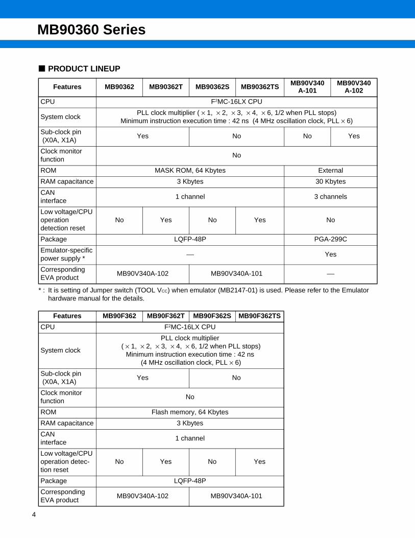
PRODUCT LINEUP
* : It is setting of Jumper switch (TOOL VCC) when emulator (MB2147-01) is used. Please refer to the Emulator hardware manual for the details.
Features MB90362 MB90362T MB90362S MB90362TS MB90V340A-101
MB90V340A-102
CPU F2MC-16LX CPU
System clockPLL clock multiplier ( × 1, × 2, × 3, × 4, × 6, 1/2 when PLL stops)
Minimum instruction execution time : 42 ns (4 MHz oscillation clock, PLL × 6)
Sub-clock pin (X0A, X1A)
Yes No No Yes
Clock monitor function
No
ROM MASK ROM, 64 Kbytes External
RAM capacitance 3 Kbytes 30 Kbytes
CANinterface
1 channel 3 channels
Low voltage/CPU operation detection reset
No Yes No Yes No
Package LQFP-48P PGA-299C
Emulator-specific power supply *
⎯ Yes
Corresponding EVA product
MB90V340A-102 MB90V340A-101 ⎯
Features MB90F362 MB90F362T MB90F362S MB90F362TS
CPU F2MC-16LX CPU
System clock
PLL clock multiplier ( × 1, × 2, × 3, × 4, × 6, 1/2 when PLL stops)
Minimum instruction execution time : 42 ns (4 MHz oscillation clock, PLL × 6)
Sub-clock pin (X0A, X1A)
Yes No
Clock monitor function
No
ROM Flash memory, 64 Kbytes
RAM capacitance 3 Kbytes
CANinterface
1 channel
Low voltage/CPU operation detec-tion reset
No Yes No Yes
Package LQFP-48P
Corresponding EVA product
MB90V340A-102 MB90V340A-101

MB90360 Series
* : It is setting of Jumper switch (TOOL VCC) when emulator (MB2147-01) is used. Please refer to the Emulator hardware manual for the details.
Features MB90367 MB90367T MB90367S MB90367TS MB90V340A-103
MB90V340A-104
CPU F2MC-16LX CPU
System clockPLL clock multiplier ( × 1, × 2, × 3, × 4, × 6, 1/2 when PLL stops)
Minimum instruction execution time : 42 ns (4 MHz oscillation clock, PLL × 6)
Sub-clock pin (X0A, X1A)
YesNo
(internal CR oscillation can be used as sub-clock) Yes
Clock monitor function
Yes
ROM MASK ROM, 64 Kbytes External
RAM capacitance 3 Kbytes 30 Kbytes
CANinterface
1 channel 3 channels
Low voltage/CPU operation detection reset
No Yes No Yes No
Package LQFP-48P PGA-299C
Emulator-specific power supply *
⎯ Yes
Corresponding EVA product
MB90V340A-104 MB90V340A-103 ⎯
Features MB90F367 MB90F367T MB90F367S MB90F367TS
CPU F2MC-16LX CPU
System clock
PLL clock multiplier ( × 1, × 2, × 3, × 4, × 6, 1/2 when PLL stops)
Minimum instruction execution time : 42 ns (4 MHz oscillation clock, PLL × 6)
Sub-clock pin (X0A, X1A)
YesNo
(internal CR oscillation can be used as sub-clock)
Clock monitor function
Yes
ROM Flash memory, 64 Kbytes
RAM capacitance 3 Kbytes
CANinterface
1 channel
Low voltage/CPU operation detection reset
No Yes No Yes
Package LQFP-48P
Corresponding EVA product
MB90V340A-104 MB90V340A-103
5

MB90360 Series
6
PIN ASSIGNMENT• MB90F362/T/S/TS, MB90362/T/S/TS, MB90F367/T/S/TS, MB90367/T/S/TS
(TOP VIEW) (LQFP-48P)
(FPT-48P-M26)
1
2
3
4
5
6
7
8
9
10
11
12
13 14 15 16 17 18 19 20 21 22 23 24
25
26
27
28
29
30
31
32
33
35
34
36
48 47 46 45 44 43 42 41 40 39 38 37
P66/AN6/PPGC(D)
AV
ss
RS
T
Vcc
Vss
C
X0A
/P40
*1
X1A
/P41
*1
P82
/SIN
0/IN
T14
R/T
IN2
P50/AN8
AVcc
P44
/FR
CK
0
P80/ADTG/INT12R
P51
/AN
9
X0
X1
P67/AN7/PPGE(F)
AVR
P60/AN0
P61/AN1
P62/AN2
P63/AN3
P64/AN4
P65/AN5 P27/IN3
P26/IN2
P25/IN1
P24/IN0
P23/PPGF(E) *2
P22/PPGD(C) *2
P21 *2
P20 *2
MD
2
MD
1
MD
0
P52
/AN
10
P53
/AN
11/T
IN3
P54
/AN
12/T
OT
3/IN
T8
P55
/AN
13/IN
T10
P56
/AN
14/IN
T11
P57
/AN
15/IN
T13
P84
/SC
K0/
INT
15R
P83
/SO
T0/
TO
T2
P42
/RX
1/IN
T9R
P43
/TX
1
P86
/SO
T1
P87
/SC
K1
P85
/SIN
1
*1 : MB90F362/T, MB90362/T, MB90F367/T, MB90367/T : X0A, X1A MB90F362S/TS, MB90362S/TS, MB90F367S/TS, MB90367S/TS : P40, P41
*2 : High current port

MB90360 Series
PIN DESCRIPTION
* : FPT-48P-M26(Continued)
Pin No.Pin name Circuit type Function
LQFP-48P*
1 AVCC I VCC power input pin for analog circuit.
2 AVR ⎯ Power (Vref+) input pin for A/D converter.It should be below VCC.
3 to 8P60 to P65
HGeneral-purpose I/O port.
AN0 to AN5 Analog input pin for A/D converter.
9, 10
P66, P67
H
General-purpose I/O port.
AN6, AN7 Analog input pin for A/D converter.
PPGC (D) , PPGE (F)
Output pin for PPG.
11
P80
F
General-purpose I/O port.
ADTG Trigger input pin for A/D converter.
INT12R External interrupt request input pin for INT12.
12 to 14P50 to P52
H
General-purpose I/O port. (P50 has different I/O circuit type from MB90V340A.)
AN8 to AN10 Analog input pin for A/D converter.
15
P53
H
General-purpose I/O port.
AN11 Analog input pin for A/D converter.
TIN3 Event input pin for reload timer 3.
16
P54
H
General-purpose I/O port.
AN12 Analog input pin for A/D converter.
TOT3 Output pin for reload timer 3
INT8 External interrupt request input pin for INT8.
17 to 19
P55 to P57
H
General-purpose I/O port.
AN13 to AN15 Analog input pin for A/D converter.
INT10, INT11, INT13
External interrupt request input pin for INT10, INT11, INT13.
20 MD2 D Input pin for operation mode specification.
21, 22MD1, MD0
C Input pin for operation mode specification.
23 RST E Reset input.
24 VCC ⎯ Power input pin (3.5 V to 5.5 V) .
25 VSS ⎯ Power input pin (0 V) .
26 C IPower supply stabilization capacitor pin. It should be connected to a higher than or equal to 0.1 µF ceramic capacitor.
7

MB90360 Series
8
* : FPT-48P-M26(Continued)
Pin No.Pin name Circuit type Function
LQFP-48P*
27 X0A
Oscillation input pin.
28 X1 Oscillation output pin.
29 to 32P27 to P24
G
General-purpose I/O port.The register can be set to select whether to use a pull-up resis-tor. This function is enabled in single-chip mode.
IN3 to IN0 Event input pin for input capture 0 to 3.
33, 34
P23, P22
J
General-purpose I/O port.The register can be set to select whether to use a pull-up resis-tor. This function is enabled in single-chip mode.High current output port.
PPGF (E) , PPGD (C)
Output pin for PPG.
35, 36 P21, P20 J
General-purpose I/O port.The register can be set to select whether to use a pull-up resis-tor. This function is enabled in single-chip mode.High current output port.
37P85
KGeneral-purpose I/O port.
SIN1 Serial data input pin for UART1.
38P87
FGeneral-purpose I/O port.
SCK1 Clock I/O pin for UART1.
39P86
FGeneral-purpose I/O port.
SOT1 Serial data output pin for UART1.
40P43
FGeneral-purpose I/O port.
TX1 TX output pin for CAN1 interface.
41
P42
F
General-purpose I/O port.
RX1 RX input pin for CAN1 interface.
INT9R External interrupt request input pin for INT9 (Sub) .
42
P83
F
General-purpose I/O port.
SOT0 Serial data output pin for UART0.
TOT2 Output pin for reload timer 2
43
P84
F
General-purpose I/O port.
SCK0 Clock I/O pin for UART0.
INT15R External interrupt request input pin for INT15.

MB90360 Series
(Continued)
* : FPT-48P-M26
Pin No.Pin name Circuit type Function
LQFP-48P*
44
P82
K
General-purpose I/O port.
SIN0 Serial data input pin for UART0.
INT14R External interrupt request input pin for INT14.
TIN2 Event input pin for reload timer 2.
45P44
F
General-purpose I/O port. (Different I/O circuit type from MB90V340A.)
FRCK0 Free-run timer 0 clock pin.
46, 47
P40, P41 FGeneral-purpose I/O port. (Devices with S-suffix and MB90V340A-101/103 only.)
X0A, X1A BOscillation input pin for sub-clock. (Devices without S-suffix and MB90V340A-102/104 only.)
48 AVSS I VSS power input pin for analog circuit.
9

MB90360 Series
10
I/O CIRCUIT TYPE
(Continued)
Type Circuit Remarks
A
Oscillation circuit• High-speed oscillation feedback
resistor = approx. 1 MΩ
B
Oscillation circuit• Low-speed oscillation feedback
resistor = approx. 10 MΩ
C
Mask ROM device : • CMOS hysteresis input pin
Flash device : • CMOS input pin
D
Mask ROM device : • CMOS hysteresis input pin• Pull-down resistor value : approx. 50 kΩ
Flash device : • CMOS input pin• No Pull-down
E
CMOS hysteresis input pin• Pull-up resistor value : approx. 50 kΩ
X1
X0
Standby control signal
Xout
Standby control signal
X1A
X0A
Xout
RHysteresisinputs
R
Pull-down
resistor
Hysteresisinputs
R
Pull-up
resistor
Hysteresisinputs

MB90360 Series
(Continued)
Type Circuit Remarks
F
• CMOS level output (IOL = 4 mA, IOH = −4 mA)
• CMOS hysteresis inputs (With thestandby-time input shutdown function)
• Automotive input (With the standby-time input shutdown function)
G
• CMOS level output (IOL = 4 mA, IOH = −4 mA)
• CMOS hysteresis inputs (With thestandby-time input shutdown function)
• Automotive input (With the standby-time input shutdown function)
• Settable pull-up resistor : approx. 50 kΩ
H
• CMOS level output (IOL = 4 mA, IOH = −4 mA)
• CMOS hysteresis inputs (With thestandby-time input shutdown function)
• Automotive input (With the standby-time input shutdown function)
• A/D analog input
Pout
Nout
R
Hysteresis inputs
Automotive inputs
Standby control forinput shutdown
R
Pull-up controlPull-up resistor
Hysteresis inputs
Automotive inputs
Pout
Nout
Standby control forinput shutdown
Pout
Nout
R
Hysteresis inputs
Analog input
Automotive inputs
Standby control forinput shutdown
11

MB90360 Series
12
(Continued)
Type Circuit Remarks
I
• Power supply input protection circuit
J
• CMOS level output (IOL = 20 mA, IOH = −14 mA)
• CMOS hysteresis inputs (With thestandby-time input shutdown function)
• Automotive input (With the standby-time input shutdown function)
• Settable pull-up resistor : approx. 50 kΩ
K
• CMOS level output (IOL = 4 mA, IOH = −4 mA)
• CMOS input (With standby-time inputshutdown function)
• Automotive input (With standby-time in-put shutdown function)
Pout high current output
Nout high current output
R
Pull-up controlPull-up resistor
Hysteresis inputs
Automotive inputs
Standby control forinput shutdown
Pout
Nout
R
CMOS inputs
Automotive inputs
Standby control forinput shutdown

MB90360 Series
HANDLING DEVICESSpecial care is required for the following when handling the device :
• Preventing latch-up• Treatment of unused pins• Using external clock• Precautions for when not using a sub-clock signal• Notes on during operation of PLL clock mode• Power supply pins (VCC/VSS) • Pull-up/down resistors• Crystal oscillator circuit• Turning-on sequence of power supply to A/D converter and analog inputs• Connection of unused pins of A/D converter• Notes on energization• Stabilization of power supply voltage• Initialization• Notes on using CAN Function• Flash security function• Correspondence with +105 °C or more
1. Preventing latch-up
CMOS IC chips may suffer latch-up under the following conditions : • A voltage higher than VCC or lower than VSS is applied to an input or output pin.• A voltage higher than the rated voltage is applied between VCC and VSS.• The AVCC power supply is applied before the VCC voltage.
Latch-up may increase the power supply current drastically, causing thermal damage to the device.
Use meticulous care not to exceed the rating.
For the same reason, also be careful not to let the analog power-supply voltage (AVCC, AVR) exceed the digitalpower-supply voltage.
2. Treatment of unused pins
Leaving unused input pins open may result in misbehavior or latch up and possible permanent damage of thedevice. Therefore, they must be pulled up or pulled down through resistors. In this case, those resistors shouldbe more than 2 kΩ .
Unused bidirectional pins should be set to the output state and can be left open, or the input state with the abovedescribed connection.
3. Using external clock
To use external clock, drive the X0 pin and leave X1 pin open.
MB90360 Series
X0
X1Open
13

MB90360 Series
14
4. Precautions for when not using a sub-clock signal
If you do not connect pins X0A and X1A to an oscillator, use pull-down handling on the X0A pin and leave theX1A pin open.
5. Notes on during operation of PLL clock mode
If the PLL clock mode is selected, the microcontroller attempts to be working with the self-oscillating circuit evenwhen there is no external oscillator or external clock input is stopped. Performance of this operation, however,cannot be guaranteed.
6. Power supply pins (VCC/VSS) • If there are multiple VCC and VSS pins, from the point of view of device design, pins to be of the same potential
are connected the inside of the device to prevent such malfunctioning as latch up.To reduce unnecessary radiation, prevent malfunctioning of the strobe signal due to the rise of ground level,and observe the standard for total output current, be sure to connect the VCC and VSS pins to the power supplyand ground externally.
• Connect VCC and VSS to the device from the current supply source at a low impedance.• As a measure against power supply noise, connect a capacitor of about 0.1 µF as a bypass capacitor between
VCC and VSS in the vicinity of VCC and VSS pins of the device.
7. Pull-up/down resistors
The MB90360 Series does not support internal pull-up/down resistors (Port 2 : built-in pull-up resistors) . Useexternal components where needed.
8. Crystal oscillator circuit
Noises around X0 or X1 pin may be possible causes of abnormal operations. Make sure to provide bypasscapacitors via shortest distance from X0, X1 pins, crystal oscillator (or ceramic resonator) and ground lines, andmake sure, to the utmost effort, that lines of oscillation circuit do not cross the lines of other circuits.
It is highly recommended to provide a printed circuit board artwork surrounding X0 and X1 pins with a groundarea for stabilizing the operation.
9. Turning-on sequence of power supply to A/D converter and analog inputs
Make sure to turn on the A/D converter power supply (AVCC and AVR) and analog inputs (AN0 to AN15) afterturning-on the digital power supply (VCC) .
Turn-off the digital power after turning off the A/D converter power supply and analog inputs. In this case, makesure that the voltage does not exceed AVRH or AVCC (turning on/off the analog and digital power suppliessimultaneously is acceptable) .
VCC
VCCVCC
VCC
VCC
VSS
VSS
VSS
VSS
VSS
MB90360Series

MB90360 Series
10. Connection of unused pins of A/D converter if A/D converter is used
Connect unused pins of A/D converter to AVCC = VCC, AVSS = AVR = VSS.
11. Notes on energization
To prevent the internal regulator circuit from malfunctioning, set the voltage rise time during energization at 50 µs or more (0.2 V to 2.7 V)
12. Stabilization of power supply voltage
A sudden change in the power supply voltage may cause the device to malfunction even within the specifiedVCC power supply voltage operating guarantee range. Therefore, the VCC power supply voltage should be stabi-lized.
For reference, the power supply voltage should be controlled so that VCC ripple variations (peak-to-peak value)at commercial frequencies (50 Hz to 60 Hz) fall below 10% of the standard VCC power supply voltage and thecoefficient of transient fluctuation does not exceed 0.1 V/ms at instantaneous power switching.
13. Initialization
In the device, there are internal registers which are initialized only by a power-on reset. To initialize these registers,turn on the power again.
14. Notes on using CAN function
To use CAN function, please set ’1’ to DIRECT bit of CAN direct mode register (CDMR) .If DIRECT bit is set to ’0’ (initial value) , wait states will be performed when accessing CAN registers.
Note : Please refer to Hardware Manual of MB90360 series for detail of CAN Direct Mode Register.
15. Flash security function
The security bit is located in the area of the flash memory.If protection code 01H is written in the security bit, the flash memory is in the protected state by security.Therefore, please do not write 01H in this address if you do not use the security function.Please refer to following table for the address of the security bit.
16. Correspondence with +105 °C or more
If used exceeding TA = +105 °C, please contact Fujitsu for reliability limitations.
Flash memory size Address for security bit
MB90F362MB90F362SMB90F362T
MB90F362TSMB90F367
MB90F367SMB90F367T
MB90F367TS
Embedded 512 Kbit Flash Memory FF0001H
15

MB90360 Series
16
BLOCK DIAGRAMS• MB90V340A-101/102
X0, X1X0A, X1A*
RST
RAM30 Kbytes
UART5 channels
DMA
SOT4 to SOT0SCK4 to SCK0SIN4 to SIN0
AVCC
AVSS
AVRHAVRLADTG
DA01, DA00
PPGF to PPG0
SDA1, SDA0
SCL1, SCL0
FRCK0
IN7 to IN0
OUT7 to OUT0
FRCK1
RX2 to RX0TX2 to TX0
TIN3 to TIN0TOT3 to TOT0
AD15 to AD00A23 to A16
ALE
RDWRLWRHHRQ
HAKRDYCLK
INT15 to INT8(INT15R to INT8R)
INT7 to INT0
CKOT
AN23 to AN0
ClockController
F2MC-16LXCore
16-bitI/O Timer 0
16-bitI/O Timer 1
InputCapture
8 channels
OutputCompare
8 channels
CANcontroller
3 channels
16-bitReload Timer
4 channels
ExternalBus
DTP/ExternalInterrupt
ClockMonitor
Prescaler (5 channels)
8/10-bitA/D
converter24 channels
10-bitD/A converter
2 channels
Inte
rnal
dat
a bu
s
8/16-bitPPG
16 channels
I2Cinterface
2 channels
* : Only for MB90V340A-102

MB90360 Series
• MB90V340A-103/104
X0, X1X0A, X1A*
RST
RAM30 Kbytes
UART5 channels
DMA
SOT4 to SOT0SCK4 to SCK0SIN4 to SIN0
AVCC
AVSS
AVRHAVRLADTG
DA01, DA00
PPGF to PPG0
SDA1, SDA0
SCL1, SCL0
FRCK0
IN7 to IN0
OUT7 to OUT0
FRCK1
RX2 to RX0TX2 to TX0
TIN3 to TIN0TOT3 to TOT0
AD15 to AD00A23 to A16
ALE
RDWRLWRHHRQ
HAKRDYCLK
INT15 to INT8(INT15R to INT8R)
INT7 to INT0
CKOT
AN23 to AN0
ClockController/
monitor
CRoscillator
circuit
16-bitI/O Timer 0
16-bitI/O Timer 1
InputCapture
8 channels
OutputCompare
8 channels
CANcontroller
3 channels
16-bitReload Timer
4 channels
ExternalBus
DTP/ExternalInterrupt
ClockMonitor
Prescaler (5 channels)
8/10-bitA/D
converter24 channels
10-bitD/A converter
2 channels
Inte
rnal
dat
a bu
s
8/16-bitPPG
16 channels
I2Cinterface
2 channels
F2MC-16LXCore
* : Only for MB90V340A-104
17

MB90360 Series
18
• MB90F362/T/S/TS, MB90362/T/S/TS, MB90F367/T/S/TS, MB90367/T/S/TS
*1 : Only for devices without S-suffix*2 : Only for devices with T-suffix*3 : CR oscillation circuit/clock monitor correspond to MB90F367/T/S/TS and MB90367/T/S/TS only.
RAM3 Kbytes
ROM64 Kbytes
UART2 channels
8/16-bitPPG
2 channels
SOT0, SOT1SCK0, SCK1SIN0, SIN1
PPGF(E), PPGD(C),PPGC(D), PPGE(F)
IN0 to IN3
FRCK0
RX1TX1
TIN2, TIN3TOT2, TOT3
INT8, INT9RINT10, INT11
INT12R, INT13INT14R, INT15R
AVCC
AVSS
AN15 to AN0
AVR
ADTG
X0, X1X0A, X1A*1
RST
ClockController/monitor *3
CRoscillator
circuit
16-bitI/O
Timer 0
InputCapture
4 channels
CANcontroller
1 channels
16-bitReloadTimer
2 channels
DTP/ExternalInterrupt
Prescaler (2 channels)
8/10-bitA/D
converter16 channels
F2MC-16LXCore
Inte
rnal
dat
a bu
s
Low voltage detection *2
CPU operation detection *2

MB90360 Series
MEMORY MAP
Note : The high-order portion of bank 00 gives the image of the FF bank ROM to make the small model of the C compiler effective. Since the low-order 16 bits are the same, the table in ROM can be referred without using the far specification in the pointer declaration.For example, an attempt to access 00C000H accesses the value at FFC000H in ROM.The ROM area in bank FF exceeds 32 Kbytes, and its entire image cannot be shown in bank 00.The image between FF8000H and FFFFFFH is visible in bank 00, while the image between FF0000H and FF7FFFH is visible only in bank FF.
FFFFFFH
FF0000H
FEFFFFH
FE0000H
FDFFFFH
FD0000H
FCFFFFH
FC0000H
FBFFFFH
FB0000H
FAFFFFH
FA0000H
F9FFFFH
0000EFH
000000H
F90000H
F8FFFFH
F80000H
00FFFFH
007FFFH
007900H
0078FFH
000100H
008000H
MB90V340A-101/102/103/104
FFFFFFH
FF0000H
0000EFH000000H
00FFFFH
007FFFH
007900H
000CFFH000100H
008000H
MB90F362/T/S/TSMB90362/T/S/TS
MB90F367/T/S/TSMB90367/T/S/TS
RAM 30 Kbytes
RAM 3 Kbytes
010000H
FEFFFFH
0000F0H0000FFH
ROM (FF bank)
ROM (FE bank)
ROM (FD bank)
ROM (FC bank)
ROM (FB bank)
ROM (FA bank)
ROM (F9 bank)
ROM (F8 bank)
ROM (image of FF bank)
Peripheral
Peripheral
ROM (FF bank)
ROM (image of FF bank)
Peripheral
Peripheral
: No access
19

MB90360 Series
20
I/O MAP (Address : 000000H-0000FFH)
(Continued)
Address Register Abbrevia-tion Access Resource name Initial value
000000H,000001H
Reserved
000002H Port 2 Data Register PDR2 R/W Port 2 XXXXXXXXB
000003H Reserved
000004H Port 4 Data Register PDR4 R/W Port 4 XXXXXXXXB
000005H Port 5 Data Register PDR5 R/W Port 5 XXXXXXXXB
000006H Port 6 Data Register PDR6 R/W Port 6 XXXXXXXXB
000007H Reserved
000008H Port 8 Data Register PDR8 R/W Port 8 XXXXXXXXB
000009H,00000AH
Reserved
00000BH Port 5 Analog Input Enable Register ADER5 R/W Port 5, A/D 11111111B
00000CH Port 6 Analog Input Enable Register ADER6 R/W Port 6, A/D 11111111B
00000DH Reserved
00000EH Input Level Select Register ILSR0 R/W Ports XXXX0XXXB
00000FH Input Level Select Register ILSR1 R/W Ports XXXXXXXXB
000010H,000011H
Reserved
000012H Port 2 Direction Register DDR2 R/W Port 2 00000000B
000013H Reserved
000014H Port 4 Direction Register DDR4 R/W Port 4 XXX00000B
000015H Port 5 Direction Register DDR5 R/W Port 5 00000000B
000016H Port 6 Direction Register DDR6 R/W Port 6 00000000B
000017H Reserved
000018H Port 8 Direction Register DDR8 R/W Port 8 000000X0B
000019H Reserved
00001AH Port A Direction Register DDRA W Port A XXX00XXXB
00001BH to
00001DH
Reserved
00001EH Port 2 Pull-up Control Register PUCR2 R/W Port 2 00000000B
00001FH Reserved

MB90360 Series
(Continued)
Address Register Abbrevia-tion Access Resource name Initial value
000020H Serial Mode Register 0 SMR0 W, R/W
UART0
00000000B
000021H Serial Control Register 0 SCR0 W, R/W 00000000B
000022H Reception/Transmission Data Register 0RDR0/TDR0
R/W 00000000B
000023H Serial Status Register 0 SSR0 R, R/W 00001000B
000024HExtended Communication Control Register 0
ECCR0R, W, R/W
000000XXB
000025H Extended Status/Control Register 0 ESCR0 R/W 00000100B
000026H Baud Rate Generator Register 00 BGR00 R/W, R 00000000B
000027H Baud Rate Generator Register 01 BGR01 R/W, R 00000000B
000028H Serial Mode Register 1 SMR1 W, R/W
UART1
00000000B
000029H Serial Control Register 1 SCR1 W, R/W 00000000B
00002AH Reception/Transmission Data Register 1RDR1/TDR1
R/W 00000000B
00002BH Serial Status Register 1 SSR1 R, R/W 00001000B
00002CHExtended Communication Control Register 1
ECCR1R, W, R/W
000000XXB
00002DH Extended Status/Control Register 1 ESCR1 R/W 00000100B
00002EH Baud Rate Generator Register 10 BGR10 R/W, R 00000000B
00002FH Baud Rate Generator Register 11 BGR11 R/W, R 00000000B
000030H to
00003AH
Reserved
00003BH Address Detect Control Register 1 PACSR1 R/WAddress Match
Detection 100000000B
00003CH to
000047H
Reserved
000048H PPG C Operation Mode Control Register PPGCC W, R/W
16-bit PPG C/D
0X000XX1B
000049H PPG D Operation Mode Control Register PPGCD W, R/W 0X000001B
00004AHPPG C/PPG D Count Clock Select Register
PPGCD R/W 000000X0B
00004BH Reserved
00004CH PPG E Operation Mode Control Register PPGCE W, R/W
16-bit PPG E/F
0X000XX1B
00004DH PPG F Operation Mode Control Register PPGCF W, R/W 0X000001B
00004EHPPG E/PPG F Count Clock Select Register
PPGEF R/W 000000X0B
00004FH Reserved
21

MB90360 Series
22
(Continued)
Address Register Abbrevia-tion Access Resource name Initial value
000050H Input Capture Control Status 0/1 ICS01 R/WInput Capture 0/1
00000000B
000051H Input Capture Edge 0/1 ICE01 R/W, R XXX0X0XXB
000052H Input Capture Control Status 2/3 ICS23 R/WInput Capture 2/3
00000000B
000053H Input Capture Edge 2/3 ICE23 R XXXXXXXXB
000054H to
000063H
Reserved
000064H Timer Control Status 2 TMCSR2 R/W 16-bit Reload Timer 2
00000000B
000065H Timer Control Status 2 TMCSR2 R/W XXXX0000B
000066H Timer Control Status 3 TMCSR3 R/W 16-bit Reload Timer 3
00000000B
000067H Timer Control Status 3 TMCSR3 R/W XXXX0000B
000068H A/D Control Status 0 ADCS0 R/W
A/D Converter
000XXXX0B
000069H A/D Control Status 1 ADCS1 R/W, W 0000000XB
00006AH A/D Data 0 ADCR0 R 00000000B
00006BH A/D Data 1 ADCR1 R XXXXXX00B
00006CH ADC Setting 0 ADSR0 R/W 00000000B
00006DH ADC Setting 1 ADSR1 R/W 00000000B
00006EHLow Voltage/CPU Operation Detection Reset Control Register
LVRC R/W, WLow voltage/CPU
operation detection reset
00111000B
00006FH ROM Mirror Function Select ROMM W ROM Mirror XXXXXXX1B
000070H to
00007FH
Reserved
000080H to
00008FH
Reserved for CAN Interface 1. Refer to “ CAN CONTROLLERS”
000090H
to 00009DH
Reserved
00009EH Address Detect Control Register 0 PACSR0 R/WAddress Match
Detection 000000000B
00009FH Delayed Interrupt/Release Register DIRR R/WDelayed Interrupt
generation moduleXXXXXXX0B
0000A0HLow-power Consumption Mode Control Register
LPMCR W, R/WLow-Power
consumption Control Circuit
00011000B
0000A1H Clock Selection Register CKSCR R, R/WLow-Power
consumptionControl Circuit
11111100B

MB90360 Series
(Continued)
Address Register Abbrevia-tion Access Resource name Initial value
0000A2H to
0000A7H
Reserved
0000A8H Watchdog Control Register WDTC R, W Watchdog Timer XXXXX111B
0000A9H Timebase Timer Control Register TBTC W, R/W Timebase Timer 1XX00100B
0000AAH Watch Timer Control register WTC R, R/W Watch Timer 1X001000B
0000ABH to
0000ADH
Reserved
0000AEH
Flash Control Status (Flash Devices only.Otherwise reserved)
FMCS R, R/W Flash Memory 000X0000B
0000AFH Reserved
0000B0H Interrupt Control Register 00 ICR00 W, R/W
Interrupt Control
00000111B
0000B1H Interrupt Control Register 01 ICR01 W, R/W 00000111B
0000B2H Interrupt Control Register 02 ICR02 W, R/W 00000111B
0000B3H Interrupt Control Register 03 ICR03 W, R/W 00000111B
0000B4H Interrupt Control Register 04 ICR04 W, R/W 00000111B
0000B5H Interrupt Control Register 05 ICR05 W, R/W 00000111B
0000B6H Interrupt Control Register 06 ICR06 W, R/W 00000111B
0000B7H Interrupt Control Register 07 ICR07 W, R/W 00000111B
0000B8H Interrupt Control Register 08 ICR08 W, R/W 00000111B
0000B9H Interrupt Control Register 09 ICR09 W, R/W 00000111B
0000BAH Interrupt Control Register 10 ICR10 W, R/W 00000111B
0000BBH Interrupt Control Register 11 ICR11 W, R/W 00000111B
0000BCH Interrupt Control Register 12 ICR12 W, R/W 00000111B
0000BDH Interrupt Control Register 13 ICR13 W, R/W 00000111B
0000BEH Interrupt Control Register 14 ICR14 W, R/W 00000111B
0000BFH Interrupt Control Register 15 ICR15 W, R/W 00000111B
0000C0H to
0000C9H
Reserved
0000CAH External Interrupt Enable 1 ENIR1 R/W
External Interrupt 1
00000000B
0000CBH External Interrupt Source 1 EIRR1 R/W XXXXXXXXB
0000CCHDetection Level Setting 1 ELVR1 R/W
00000000B
0000CDH 00000000B
0000CEH External Interrupt Source Select EISSR R/W 00000000B
23

MB90360 Series
24
(Continued)
Address Register Abbrevia-tion Access Resource name Initial value
0000CFH PLL/Subclock Control Register PSCCR W PLL XXXX0000B
0000D0H to
0000FFH
Reserved

MB90360 Series
(Address : 7900H-7FFFH)
(Continued)
Address Register Abbrevia-tion Access Resource name Initial value
7900H
to 7917H
Reserved
7918H Reload Register LC PRLLC R/W
16-bit PPG C/D
XXXXXXXXB
7919H Reload Register HC PRLHC R/W XXXXXXXXB
791AH Reload Register LD PRLLD R/W XXXXXXXXB
791BH Reload Register HD PRLHD R/W XXXXXXXXB
791CH Reload Register LE PRLLE R/W
16-bit PPG E/F
XXXXXXXXB
791DH Reload Register HE PRLHE R/W XXXXXXXXB
791EH Reload Register LF PRLLF R/W XXXXXXXXB
791FH Reload Register HF PRLHF R/W XXXXXXXXB
7920H Input Capture 0 IPCP0 R
Input Capture 0/1
XXXXXXXXB
7921H Input Capture 0 IPCP0 R XXXXXXXXB
7922H Input Capture 1 IPCP1 R XXXXXXXXB
7923H Input Capture 1 IPCP1 R XXXXXXXXB
7924H Input Capture 2 IPCP2 R
Input Capture 2/3
XXXXXXXXB
7925H Input Capture 2 IPCP2 R XXXXXXXXB
7926H Input Capture 3 IPCP3 R XXXXXXXXB
7927H Input Capture 3 IPCP3 R XXXXXXXXB
7928H
to 793FH
Reserved
7940H Timer Data 0 TCDT0 R/W
I/O Timer 0
00000000B
7941H Timer Data 0 TCDT0 R/W 00000000B
7942H Timer Control Status 0 TCCSL0 R/W 00000000B
7943H Timer Control Status 0 TCCSH0 R/W 0XXXXXXXB
7944H
to 794BH
Reserved
794CHTimer 2/Reload 2
TMR2/TMRLR2
R/W 16-bit Reload Timer 2
XXXXXXXXB
794DH R/W XXXXXXXXB
794EHTimer 3/Reload 3
TMR3/TMRLR3
R/W 16-bit Reload Timer 3
XXXXXXXXB
794FH R/W XXXXXXXXB
7950H
to 795FH
Reserved
25

MB90360 Series
26
(Continued)
Address Register Abbrevia-tion Access Resource name Initial value
7960HClock Monitor Function Control Register
CSVCR R, R/W Clock monitor 00011100B
7961H
to 796DH
Reserved
796EHCAN Direct Mode Register (MB90V340 only)
CDMR R/W CAN clock sync XXXXXXX0B
796FH
to 79DFH
Reserved
79E0H Detect Address Setting 0 PADR0 R/W
Address Match Detection 0
XXXXXXXXB
79E1H Detect Address Setting 0 PADR0 R/W XXXXXXXXB
79E2H Detect Address Setting 0 PADR0 R/W XXXXXXXXB
79E3H Detect Address Setting 1 PADR1 R/W XXXXXXXXB
79E4H Detect Address Setting 1 PADR1 R/W XXXXXXXXB
79E5H Detect Address Setting 1 PADR1 R/W XXXXXXXXB
79E6H Detect Address Setting 2 PADR2 R/W XXXXXXXXB
79E7H Detect Address Setting 2 PADR2 R/W XXXXXXXXB
79E8H Detect Address Setting 2 PADR2 R/W XXXXXXXXB
79E9H
to 79EFH
Reserved
79F0H Detect Address Setting 3 PADR3 R/W
Address Match Detection 1
XXXXXXXXB
79F1H Detect Address Setting 3 PADR3 R/W XXXXXXXXB
79F2H Detect Address Setting 3 PADR3 R/W XXXXXXXXB
79F3H Detect Address Setting 4 PADR4 R/W XXXXXXXXB
79F4H Detect Address Setting 4 PADR4 R/W XXXXXXXXB
79F5H Detect Address Setting 4 PADR4 R/W XXXXXXXXB
79F6H Detect Address Setting 5 PADR5 R/W XXXXXXXXB
79F7H Detect Address Setting 5 PADR5 R/W XXXXXXXXB
79F8H Detect Address Setting 5 PADR5 R/W XXXXXXXXB
79F9H
to 7BFFH
Reserved
7C00H
to 7CFFH
Reserved for CAN Interface 1. Refer to “ CAN CONTROLLERS”

MB90360 Series
(Continued)
Notes : • Initial value of “X” represents unknown value.• Any write access to reserved addresses in I/O map should not be performed. A read access to reserved
addresses results in reading “X”.
Address Register Abbrevia-tion Access Resource name Initial value
7D00H
to 7DFFH
Reserved for CAN Interface 1. Refer to “ CAN CONTROLLERS”
7E00H
to 7FFFH
Reserved
27

MB90360 Series
28
CAN CONTROLLERSThe CAN controller has the following features : • Conforms to CAN Specification Version 2.0 Part A and B
• Supports transmission/reception in standard frame and extended frame formats• Supports transmitting of data frames by receiving remote frames• 16 transmitting/receiving message buffers
• 29-bit ID and 8-byte data• Multi-level message buffer configuration
• Provides full-bit comparison, full-bit mask, acceptance register 0/acceptance register 1 for each messagebuffer as ID acceptance mask• 2 acceptance mask registers in either standard frame format or extended frame formats
• Bit rate programmable from 10 Kbps/s to 2 Mbps/s (when input clock is at 16 MHz)
List of Control Registers (1)
AddressRegister Abbreviation Access Initial Value
CAN1
000080H Message buffervalid register
BVALR R/W00000000B 00000000B000081H
000082H Transmit requestregister
TREQR R/W00000000B 00000000B000083H
000084H Transmit cancelregister
TCANR W00000000B 00000000B000085H
000086H Transmission complete register
TCR R/W00000000B 00000000B000087H
000088H Receive complete register
RCR R/W00000000B 00000000B000089H
00008AH Remote request receiving register
RRTRR R/W00000000B 00000000B00008BH
00008CH Receive overrunregister
ROVRR R/W00000000B 00000000B00008DH
00008EH Reception interrupt enable register
RIER R/W00000000B 00000000B00008FH

MB90360 Series
List of Control Registers (2)
AddressRegister Abbreviation Access Initial Value
CAN1
007D00H Control statusregister
CSRR/W, WR/W, R
0XXXX0X1B
00XXX000B007D01H
007D02H Last eventindicator register
LEIR R/W000X0000B
XXXXXXXXB007D03H
007D04H Receive and transmit error counter
RTEC R00000000B 00000000B007D05H
007D06H Bit timingregister
BTR R/W11111111B X1111111B007D07H
007D08HIDE register IDER R/W
XXXXXXXXB XXXXXXXXB007D09H
007D0AH Transmit RTRregister
TRTRR R/W00000000B 00000000B007D0BH
007D0CH Remote frame receive waiting
registerRFWTR R/W
XXXXXXXXB XXXXXXXXB007D0DH
007D0EH Transmit interrupt enable register
TIER R/W00000000B 00000000B007D0FH
007D10H
Acceptance mask select register
AMSR R/W
XXXXXXXXB XXXXXXXXB007D11H
007D12H XXXXXXXXB XXXXXXXXB007D13H
007D14H
Acceptance mask register 0
AMR0 R/W
XXXXXXXXB XXXXXXXXB007D15H
007D16H XXXXXXXXB
XXXXXXXXB007D17H
007D18H
Acceptance mask register 1
AMR1 R/W
XXXXXXXXB XXXXXXXXB007D19H
007D1AH XXXXXXXXB
XXXXXXXXB007D1BH
29

MB90360 Series
30
List of Message Buffers (ID Registers) (1)
AddressRegister Abbreviation Access Initial Value
CAN1
007C00H
to007C1FH
General-purpose RAM ⎯ R/WXXXXXXXXB
toXXXXXXXXB
007C20H
ID register 0 IDR0 R/W
XXXXXXXXB XXXXXXXXB007C21H
007C22H XXXXXXXXB XXXXXXXXB007C23H
007C24H
ID register 1 IDR1 R/W
XXXXXXXXB XXXXXXXXB007C25H
007C26H XXXXXXXXB XXXXXXXXB007C27H
007C28H
ID register 2 IDR2 R/W
XXXXXXXXB XXXXXXXXB007C29H
007C2AH XXXXXXXXB XXXXXXXXB007C2BH
007C2CH
ID register 3 IDR3 R/W
XXXXXXXXB XXXXXXXXB007C2DH
007C2EH XXXXXXXXB XXXXXXXXB007C2FH
007C30H
ID register 4 IDR4 R/W
XXXXXXXXB XXXXXXXXB007C31H
007C32H XXXXXXXXB XXXXXXXXB007C33H
007C34H
ID register 5 IDR5 R/W
XXXXXXXXB XXXXXXXXB007C35H
007C36H XXXXXXXXB XXXXXXXXB007C37H
007C38H
ID register 6 IDR6 R/W
XXXXXXXXB XXXXXXXXB007C39H
007C3AH XXXXXXXXB XXXXXXXXB007C3BH
007C3CH
ID register 7 IDR7 R/W
XXXXXXXXB XXXXXXXXB007C3DH
007C3EH XXXXXXXXB XXXXXXXXB007C3FH

MB90360 Series
List of Message Buffers (ID Registers) (2)
AddressRegister Abbreviation Access Initial Value
CAN1
007C40H
ID register 8 IDR8 R/W
XXXXXXXXB XXXXXXXXB007C41H
007C42H XXXXXXXXB XXXXXXXXB007C43H
007C44H
ID register 9 IDR9 R/W
XXXXXXXXB XXXXXXXXB007C45H
007C46H XXXXXXXXB XXXXXXXXB007C47H
007C48H
ID register 10 IDR10 R/W
XXXXXXXXB XXXXXXXXB007C49H
007C4AH XXXXXXXXB XXXXXXXXB007C4BH
007C4CH
ID register 11 IDR11 R/W
XXXXXXXXB XXXXXXXXB007C4DH
007C4EH XXXXXXXXB XXXXXXXXB007C4FH
007C50H
ID register 12 IDR12 R/W
XXXXXXXXB XXXXXXXXB007C51H
007C52H XXXXXXXXB XXXXXXXXB007C53H
007C54H
ID register 13 IDR13 R/W
XXXXXXXXB XXXXXXXXB007C55H
007C56H XXXXXXXXB XXXXXXXXB007C57H
007C58H
ID register 14 IDR14 R/W
XXXXXXXXB XXXXXXXXB007C59H
007C5AH XXXXXXXXB XXXXXXXXB007C5BH
007C5CH
ID register 15 IDR15 R/W
XXXXXXXXB XXXXXXXXB007C5DH
007C5EH XXXXXXXXB XXXXXXXXB007C5FH
31

MB90360 Series
32
List of Message Buffers (DLC Registers and Data Registers) (1)
AddressRegister Abbreviation Access Initial Value
CAN1
007C60HDLC register 0 DLCR0 R/W XXXXXXXXB
007C61H
007C62HDLC register 1 DLCR1 R/W XXXXXXXXB
007C63H
007C64HDLC register 2 DLCR2 R/W XXXXXXXXB
007C65H
007C66HDLC register 3 DLCR3 R/W XXXXXXXXB
007C67H
007C68HDLC register 4 DLCR4 R/W XXXXXXXXB
007C69H
007C6AHDLC register 5 DLCR5 R/W XXXXXXXXB
007C6BH
007C6CHDLC register 6 DLCR6 R/W XXXXXXXXB
007C6DH
007C6EHDLC register 7 DLCR7 R/W XXXXXXXXB
007C6FH
007C70HDLC register 8 DLCR8 R/W XXXXXXXXB
007C71H
007C72HDLC register 9 DLCR9 R/W XXXXXXXXB
007C73H
007C74HDLC register 10 DLCR10 R/W XXXXXXXXB
007C75H
007C76HDLC register 11 DLCR11 R/W XXXXXXXXB
007C77H
007C78HDLC register 12 DLCR12 R/W XXXXXXXXB
007C79H
007C7AHDLC register 13 DLCR13 R/W XXXXXXXXB
007C7BH
007C7CHDLC register 14 DLCR14 R/W XXXXXXXXB
007C7DH
007C7EHDLC register 15 DLCR15 R/W XXXXXXXXB
007C7FH

MB90360 Series
List of Message Buffers (DLC Registers and Data Registers) (2)
AddressRegister Abbreviation Access Initial Value
CAN1
007C80H
to 007C87H
Data register 0 (8 bytes)
DTR0 R/WXXXXXXXXB
to XXXXXXXXB
007C88H
to 007C8FH
Data register 1 (8 bytes)
DTR1 R/WXXXXXXXXB
to XXXXXXXXB
007C90H
to 007C97H
Data register 2 (8 bytes)
DTR2 R/WXXXXXXXXB
to XXXXXXXXB
007C98H
to 007C9FH
Data register 3 (8 bytes)
DTR3 R/WXXXXXXXXB
to XXXXXXXXB
007CA0H
to 007CA7H
Data register 4 (8 bytes)
DTR4 R/WXXXXXXXXB
to XXXXXXXXB
007CA8H
to 007CAFH
Data register 5 (8 bytes)
DTR5 R/WXXXXXXXXB
to XXXXXXXXB
007CB0H
to 007CB7H
Data register 6 (8 bytes)
DTR6 R/WXXXXXXXXB
to XXXXXXXXB
007CB8H
to 007CBFH
Data register 7 (8 bytes)
DTR7 R/WXXXXXXXXB
to XXXXXXXXB
007CC0H
to 007CC7H
Data register 8 (8 bytes)
DTR8 R/WXXXXXXXXB
to XXXXXXXXB
007CC8H
to 007CCFH
Data register 9 (8 bytes)
DTR9 R/WXXXXXXXXB
to XXXXXXXXB
007CD0H
to 007CD7H
Data register 10 (8 bytes)
DTR10 R/WXXXXXXXXB
to XXXXXXXXB
007CD8H
to 007CDFH
Data register 11 (8 bytes)
DTR11 R/WXXXXXXXXB
to XXXXXXXXB
007CE0H
to 007CE7H
Data register 12 (8 bytes)
DTR12 R/WXXXXXXXXB
to XXXXXXXXB
007CE8H
to 007CEFH
Data register 13 (8 bytes)
DTR13 R/WXXXXXXXXB
to XXXXXXXXB
33

MB90360 Series
34
List of Message Buffers (DLC Registers and Data Registers) (3)
AddressRegister Abbreviation Access Initial Value
CAN1
007CF0H
to 007CF7H
Data register 14 (8 bytes)
DTR14 R/WXXXXXXXXB
to XXXXXXXXB
007CF8H
to 007CFFH
Data register 15 (8 bytes)
DTR15 R/WXXXXXXXXB
to XXXXXXXXB
MB90360 Series
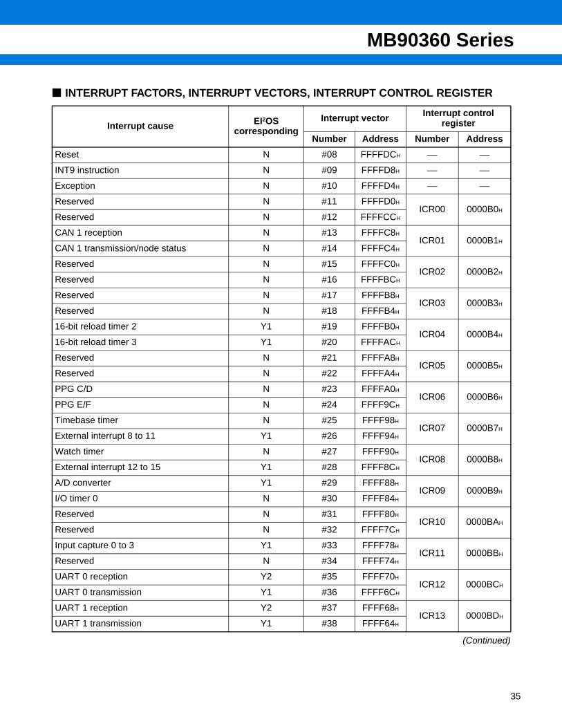
INTERRUPT FACTORS, INTERRUPT VECTORS, INTERRUPT CONTROL REGISTER
(Continued)
Interrupt cause EI2OS corresponding
Interrupt vector Interrupt control register
Number Address Number Address
Reset N #08 FFFFDCH ⎯ ⎯
INT9 instruction N #09 FFFFD8H ⎯ ⎯
Exception N #10 FFFFD4H ⎯ ⎯
Reserved N #11 FFFFD0HICR00 0000B0H
Reserved N #12 FFFFCCH
CAN 1 reception N #13 FFFFC8HICR01 0000B1H
CAN 1 transmission/node status N #14 FFFFC4H
Reserved N #15 FFFFC0HICR02 0000B2H
Reserved N #16 FFFFBCH
Reserved N #17 FFFFB8HICR03 0000B3H
Reserved N #18 FFFFB4H
16-bit reload timer 2 Y1 #19 FFFFB0HICR04 0000B4H
16-bit reload timer 3 Y1 #20 FFFFACH
Reserved N #21 FFFFA8HICR05 0000B5H
Reserved N #22 FFFFA4H
PPG C/D N #23 FFFFA0HICR06 0000B6H
PPG E/F N #24 FFFF9CH
Timebase timer N #25 FFFF98HICR07 0000B7H
External interrupt 8 to 11 Y1 #26 FFFF94H
Watch timer N #27 FFFF90HICR08 0000B8H
External interrupt 12 to 15 Y1 #28 FFFF8CH
A/D converter Y1 #29 FFFF88HICR09 0000B9H
I/O timer 0 N #30 FFFF84H
Reserved N #31 FFFF80HICR10 0000BAH
Reserved N #32 FFFF7CH
Input capture 0 to 3 Y1 #33 FFFF78HICR11 0000BBH
Reserved N #34 FFFF74H
UART 0 reception Y2 #35 FFFF70HICR12 0000BCH
UART 0 transmission Y1 #36 FFFF6CH
UART 1 reception Y2 #37 FFFF68HICR13 0000BDH
UART 1 transmission Y1 #38 FFFF64H
35

MB90360 Series
36
(Continued)
Y1 : Usable
Y2 : Usable, with EI2OS stop function
N : Unusable
Notes : • The peripheral resources sharing the ICR register have the same interrupt level.• When 2 peripheral resources share the ICR register, only one can use extended intelligent I/O service
at a time.• When either of the 2 peripheral resources sharing the ICR register specifies extended intelligent I/O
service, the other one cannot use interrupts.
Interrupt cause EI2OScorresponding
Interrupt vector Interrupt control register
Number Address Number Address
Reserved N #39 FFFF60HICR14 0000BEH
Reserved N #40 FFFF5CH
Flash memory N #41 FFFF58HICR15 0000BFH
Delayed interrupt generation module N #42 FFFF54H

MB90360 Series
ELECTRICAL CHARACTERISTICS1. Absolute Maximum Ratings
(Continued)
Parameter SymbolRating
Unit RemarksMin Max
Power supply voltage*1
VCC VSS − 0.3 VSS + 6.0 V
AVCC VSS − 0.3 VSS + 6.0 V VCC = AVCC*2
AVR VSS − 0.3 VSS + 6.0 V AVCC ≥ AVR*2
Input voltage*1 VI VSS − 0.3 VSS + 6.0 V *3
Output voltage*1 VO VSS − 0.3 VSS + 6.0 V *3
Maximum clamp current ICLAMP −2.0 +2.0 mA *6
Total Maximum clamp current Σ|ICLAMP| ⎯ 40 mA *6
“L” level maximum output currentIOL1 ⎯ 15 mA *4
IOL2 ⎯ 40 mA *5
“L” level average output currentIOLAV1 ⎯ 4 mA *4
IOLAV2 ⎯ 30 mA *5
“L” level maximum overall output currentΣIOL1 ⎯ 125 mA *4
ΣIOL2 ⎯ 160 mA *5
“L” level average overall output current
ΣIOLAV1⎯ 40 mA
*4 +105 °C < TA ≤ +125 °C
ΣIOLAV2 *5 +105 °C < TA ≤ +125 °C
ΣIOLAV1⎯ 40 mA
*4 −40 °C ≤ TA ≤ +105 °C
ΣIOLAV2 *5 −40 °C ≤ TA ≤ +105 °C
“H” level maximum output currentIOH1 ⎯ −15 mA *4
IOH2 ⎯ −40 mA *5
“H” level average output currentIOHAV1 ⎯ −4 mA *4
IOHAV2 ⎯ −30 mA *5
“H” level maximum overall output currentΣIOH1 ⎯ −125 mA *4
ΣIOH2 ⎯ −160 mA *5
“H” level average overall output current
ΣIOHAV1⎯ −40 mA
*4 +105 °C < TA ≤ +125 °C
ΣIOHAV2 *5 +105 °C < TA ≤ +125 °C
ΣIOHAV1⎯ −40 mA
*4 −40 °C ≤ TA ≤ +105 °C
ΣIOHAV2 *5 −40 °C ≤ TA ≤ +105 °C
Power consumption PD ⎯ 300 mWMB90F362/T/S/TS, MB90F367/T/S/TS
Operating temperature TA−40 +105 °C
−40 +125 °C *7
Storage temperature TSTG −55 +150 °C
37

MB90360 Series
38
(Continued)
*1 : This parameter is based on VSS = AVSS = 0 V.
*2 : Set AVCC and VCC to the same voltage. Make sure that AVCC does not exceed VCC and that the voltage at the analog inputs does not exceed AVCC when the power is switched on.
*3 : VI and VO should not exceed VCC + 0.3 V. VI should not exceed the specified ratings. However, if the maximun current to/from an input is limited by some means with external components, the ICLAMP rating supersedes the VI rating.
*4 : Applicable to pins : P24 to P27, P40 to P44, P50 to P57, P60 to P67, P80, P82 to P87
*5 : Applicable to pins : P20 to P23
*6 : Applicable to pins : P20 to P27, P40 to P44, P50 to P57, P60 to P67, P80, P82 to P87• Use within recommended operating conditions.• Use at DC voltage (current) .• The +B signal should always be applied a limiting resistance placed between the +B signal and the
microcontroller.• The value of the limiting resistance should be set so that when the +B signal is applied the input current to
the microcontroller pin does not exceed rated values, either instantaneously or for prolonged periods.• Note that when the microcontroller drive current is low, such as in the power saving modes, the +B input
potential may pass through the protective diode and increase the potential at the VCC pin, and this may affectother devices.
• Note that if a +B signal is inputted when the microcontroller power supply is off (not fixed at 0 V) , the powersupply is provided from the pins, so that incomplete operation may result.
• Note that if the +B input is applied during power-on, the power supply is provided from the pins and the resulting power supply voltage may not be sufficient to operate the power-on reset.
• Care must be taken not to leave the +B input pin open.• Sample recommended circuits :
*7 : If used exceeding TA = +105 °C, please contact Fujitsu for reliability limitations.
WARNING: Semiconductor devices can be permanently damaged by application of stress (voltage, current, temperature, etc.) in excess of absolute maximum ratings. Do not exceed these ratings.
Pch
Nch
VCC
R
• Input/output equivalent circuits
+B input (0 V to 16 V)
Limitingresistance
Protective diode

MB90360 Series
2. Recommended Conditions (VSS = AVSS = 0 V)
* : If used exceeding TA = +105 °C, please contact Fujitsu for reliability limitations.
WARNING: The recommended operating conditions are required in order to ensure the normal operation of thesemiconductor device. All of the device’s electrical characteristics are warranted when the device isoperated within these ranges.
Always use semiconductor devices within their recommended operating condition ranges. Operationoutside these ranges may adversely affect reliability and could result in device failure.No warranty is made with respect to uses, operating conditions, or combinations not represented onthe data sheet. Users considering application outside the listed conditions are advised to contact theirFUJITSU representatives beforehand.
Parameter SymbolValue
Unit RemarksMin Typ Max
Power supply voltageVCC, AVCC
4.0 5.0 5.5 V Under normal operation
3.5 5.0 5.5 VUnder normal operation when not using the A/D converter and not Flash programming.
3.0 ⎯ 5.5 V Maintains RAM data in stop mode
Smooth capacitor CS 0.1 ⎯ 1.0 µF
Use a ceramic capacitor or capac-itor of better AC characteristics. Bypass capacitor at the VCC pin should be greater than this capac-itor.
Operating temperature TA−40 ⎯ +105 °C
−40 ⎯ +125 °C *
C
CS
• C Pin Connection Diagram
39

MB90360 Series
40
3. DC Characteristics (TA = −40 °C to +125 °C, VCC = 5.0 V ± 10%, fCP ≤ 24 MHz, VSS = AVSS = 0 V)
(Continued)
Parameter Sym-bol Pin Condition
ValueUnit Remarks
Min Typ Max
Input “H” voltage
VIHS ⎯ ⎯ 0.8 VCC ⎯ VCC + 0.3 V
Pin inputs if CMOS hysteresis input levels are selected (except P82, P85)
VIHA ⎯ ⎯ 0.8 VCC ⎯ VCC + 0.3 VPin inputs if Automotive input levels are selected
VIHS ⎯ ⎯ 0.7 VCC ⎯ VCC + 0.3 VP82, P85 inputs if CMOS input levels are selected
VIHR ⎯ ⎯ 0.8 VCC ⎯ VCC + 0.3 VRST input pin (CMOS hysteresis)
VIHM ⎯ ⎯ VCC − 0.3 ⎯ VCC + 0.3 V MD input pin
Input “L” voltage
VILS ⎯ ⎯ VSS − 0.3 ⎯ 0.2 VCC V
Pin inputs if CMOS hysteresis input levels are selected (except P82, P85)
VILA ⎯ ⎯ VSS − 0.3 ⎯ 0.5 VCC VPin inputs if Automotive input levels are selected
VILS ⎯ ⎯ VSS − 0.3 ⎯ 0.3 VCC VP82, P85 inputs if CMOS input levels are selected
VILR ⎯ ⎯ VSS − 0.3 ⎯ 0.2 VCC VRST input pin (CMOS hysteresis)
VILM ⎯ ⎯ VSS − 0.3 ⎯ VSS + 0.3 V MD input pin
Output “H” voltage
VOHOther than P20 to P23
VCC = 4.5 V, IOH = −4.0 mA
VCC − 0.5 ⎯ ⎯ V
Output “H” voltage
VOHI P20 to P23VCC = 4.5 V, IOH = −14.0 mA
VCC − 0.5 ⎯ ⎯ V
Output “L” voltage
VOLOther than P20 to P23
VCC = 4.5 V, IOL = 4.0 mA
⎯ ⎯ 0.4 V
Output “L” voltage
VOLI P20 to P23VCC = 4.5 V, IOL = 20.0 mA
⎯ ⎯ 0.4 V
Input leak current
IIL ⎯ VCC = 5.5 V, VSS < VI < VCC
−1 ⎯ 1 µA
Pull-up resistance
RUPP20 to P27, RST
⎯ 25 50 100 kΩ
Pull-down resistance
RDOWN MD2 ⎯ 25 50 100 kΩ Except Flash devices

MB90360 Series
(TA = −40 °C to +125 °C, VCC = 5.0 V ± 10%, fCP ≤ 24 MHz, VSS = AVSS = 0 V)
* : The power supply current is measured with an external clock.(Continued)
Parameter Sym-bol Pin Condition
ValueUnit Remarks
Min Typ Max
Power supply current*
ICC
VCC
VCC = 5.0 V, Internal frequency : 24 MHz, At normal operation.
⎯ 35 45 mA
VCC = 5.0 V, Internal frequency : 24 MHz, At writing FLASH memory.
⎯ 50 60 mA Flash devices
VCC = 5.0 V, Internal frequency : 24 MHz, At erasing FLASH memory.
⎯ 50 60 mA Flash devices
ICCS
VCC = 5.0 V, Internal frequency : 24 MHz, At sleep mode.
⎯ 12 20 mA
ICTS
VCC = 5.0 V, Internal frequency : 2 MHz, At main timer mode
⎯ 0.3 0.8mA
Without T model
⎯ 0.4 1.0 With T model
ICTSPLL6
VCC = 5.0 V, Internal frequency : 24 MHz, At PLL timer mode, External frequency = 4 MHz
⎯ 4 7 mA
ICCL
VCC = 5.0 VInternal frequency : 8 kHz, At sub operation, TA = +25°C
Stopping clock monitor function ⎯ 40 100
µA
MB90F362, MB90F367, MB90362, MB90367
Operating clock monitor function ⎯ 60 150 MB90F367, MB90367
Stopping clock monitor function ⎯ 90 200 MB90F362T, MB90F367T,
MB90362T, MB90367T
Operating clock monitor function ⎯ 110 250 MB90F367T, MB90367T
ICCLS
VCC = 5.0 VInternal frequency : 8 kHz, At sub sleep, TA = +25°C
Stopping clock monitor function ⎯ 10 50
µA
MB90F362, MB90F367, MB90362, MB90367
Operating clock monitor function ⎯ 30 100 MB90F367, MB90367
Stopping clock monitor function ⎯ 60 150 MB90F362T, MB90F367T,
MB90362T, MB90367T
Operating clock monitor function ⎯ 80 200 MB90F367T, MB90367T
ICCT
VCC = 5.0 VInternal frequency : 8 kHz, At watch mode, TA = +25°C
Stopping clock monitor function ⎯ 8 30
µA
MB90F362, MB90F367, MB90362, MB90367
Operating clock monitor function ⎯ 30 70 MB90F367, MB90367
Stopping clock monitor function ⎯ 60 130 MB90F362T, MB90F367T,
MB90362T, MB90367T
Operating clock monitor function ⎯ 80 170 MB90F367T, MB90367T
ICCHVCC = 5.0 V, At stop mode, TA = +25°C
⎯ 5 25 µA Without T model
⎯ 50 130 µA With T model
41

MB90360 Series
42
(Continued) (TA = −40 °C to +125 °C, VCC = 5.0 V ± 10%, fCP ≤ 24 MHz, VSS = AVSS = 0 V)
Parameter Sym-bol Pin Condition
ValueUnit Remarks
Min Typ Max
Input capacity CIN
Other than AVCC, AVSS, AVR, VCC, VSS, C
⎯ ⎯ 5 15 pF

MB90360 Series
4. AC Characteristics
(1) Clock Timing (TA = −40 °C to +125 °C, VCC = 5.0 V ± 10%, fCP ≤ 24 MHz, VSS = AVSS = 0 V)
Parameter Symbol PinValue
Unit RemarksMin Typ Max
Clock frequencyfC
X0, X1
3 ⎯ 16 MHz1/2 when PLL stops,When using an oscillation circuit
4 ⎯ 16 MHzPLL × 1, When using an oscillation circuit
4 ⎯ 12 MHzPLL × 2, When using an oscillation circuit
4 ⎯ 8 MHzPLL × 3, When using an oscillation circuit
4 ⎯ 6 MHzPLL × 4, When using an oscillation circuit
4 ⎯ 4 MHzPLL × 6, When using an oscillation circuit
X0, X1
3 ⎯ 24 MHz1/2 when PLL stops,When using an external clock
4 ⎯ 24 MHzPLL × 1, When using an external clock
4 ⎯ 12 MHzPLL × 2, When using an external clock
4 ⎯ 8 MHzPLL × 3, When using an external clock
4 ⎯ 6 MHzPLL × 4, When using an external clock
4 ⎯ 4 MHzPLL × 6, When using an external clock
fCL X0A, X1A — 32.768 100 kHz
Clock cycle timetCYL
X0, X1 62.5 ⎯ 333 ns When using an oscillation circuit
X0, X1 41.67 ⎯ 333 ns When using an external clock
tCYLL X0A, X1A 10 30.5 — µs
Input clock pulse widthPWH, PWL X0 10 ⎯ ⎯ ns
Duty ratio is about 30% to 70%.PWHL, PWLL X0A 5 15.2 ⎯ µs
Input clock rise and fall time
tCR, tCF X0 ⎯ ⎯ 5 ns When using external clock
Internal operating clock frequency (machine clock)
fCP ⎯ 1.5 ⎯ 24 MHz When using main clock
fCPL ⎯ ⎯ 8.192 50 kHz When using sub clock
Internal operating clock cycle time (machine clock)
tCP ⎯ 41.67 ⎯ 666 ns When using main clock
tCPL ⎯ 20 122.1 ⎯ µs When using sub clock
43

MB90360 Series
44
X0
tCYL
tCF tCR
0.8 VCC
0.2 VCC
PWH PWL
X0A
tCYLL
tCF tCR
0.8 VCC
0.2 VCC
PWHL PWLL
• Clock Timing

MB90360 Series
Guaranteed operation range of MB90360 series
* : When using the oscillation circuit, the maximum oscillation clock frequency is 16 MHz.
5.5
3.5
41.5 24
4.0
Guaranteed operation range
Guaranteed PLL operation range
Guaranteed A/D converteroperation range
Internal clock fCP (MHz)
Pow
er s
uppl
y vo
ltage
VC
C (
V)
• Guaranteed PLL Operation Range
24
16
12
8
4.0
1.5
3 4 8 2412
×1/2
16
Guaranteed oscillation frequency range
External clock fC (MHz) *
Inte
rnal
clo
ck f C
P (
MH
z)
(PLL off)
× 6 × 4 × 3 × 2 × 1
45

MB90360 Series
46
(2) Reset Standby Input (TA = −40 °C to +125 °C, VCC = 5.0 V ± 10%, fCP ≤ 24 MHz, VSS = AVSS = 0 V)
* : Oscillation time of oscillator is the time that the amplitude reaches 90%.In the crystal oscillator, the oscillation time is between several ms and tens of ms. In FAR / ceramic oscillators, the oscillation time is between hundreds of µs and several ms. With an external clock, the oscillation time is 0 ms.
Parameter Symbol PinValue
Unit RemarksMin Max
Reset input time
tRSTL RST
500 ⎯ ns Under normal operation
Oscillation time of oscillator* + 100 µs
⎯ nsIn stop mode, sub clock mode, sub sleep mode and watch mode
100 ⎯ µs In timebase timer mode
RST
X0
tRSTL
0.2 VCC 0.2 VCC
100 µs
90% ofamplitude
Instruction execution
Oscillation stabilization waiting time
Oscillation timeof oscillator
Internal operationclock
Internal reset
RST
0.2 VCC
tRSTL
0.2 VCC
• Under normal operation :
• In stop mode, sub clock mode, sub sleep mode, watch mode :

MB90360 Series
(3) Power-on Reset (TA = −40 °C to +125 °C, VCC = 5.0 V ± 10%, fCP ≤ 24 MHz, VSS = AVSS = 0 V)
Parameter Symbol Pin ConditionValue
Unit RemarksMin Max
Power on rise time tR VCC⎯
0.05 30 ms
Power off time tOFF VCC 1 ⎯ ms Due to repetitive operation
VCC
VCC
VSS
3 V
tR
tOFF
2.7 V
0.2 V 0.2 V0.2 V
Holds RAM data
If you change the power supply voltage too rapidly, a power-on reset may occur. We recommend that you start up smoothly by restraining voltages when changing the power supply voltage during operation, as shown in the figure below. Perform while not using the PLL clock. However, if voltage drops are within 1 V/s, you can operate while using the PLL clock.
We recommend a rise of 50 mV/ms maximum.
47

MB90360 Series
48
(4) UART0/1 (TA = −40 °C to +125 °C, VCC = 5.0 V ± 10%, fCP ≤ 24 MHz, VSS = 0 V)
Notes : • AC characteristic in CLK synchronized mode.• CL is load capacity value of pins when testing.• tCP is internal operating clock cycle time (machine clock) . Refer to “ (1) Clock Timing”.
Parameter Symbol Pin ConditionValue
Unit RemarksMin Max
Serial clock cycle time tSCYC SCK0, SCK1
Internal shift clock mode output pins are CL = 80 pF + 1 TTL.
8 tCP ⎯ ns
SCK ↓ → SOT delay time tSLOVSCK0, SCK1, SOT0, SOT1
−80 +80 ns
Valid SIN → SCK ↑ tIVSHSCK0, SCK1, SIN0, SIN1
100 ⎯ ns
SCK ↑ → Valid SIN hold time tSHIXSCK0, SCK1, SIN0, SIN1
60 ⎯ ns
Serial clock “H” pulse width tSHSL SCK0, SCK1
External shift clock mode output pins are CL = 80 pF + 1 TTL.
4 tCP ⎯ ns
Serial clock “L” pulse width tSLSH SCK0, SCK1 4 tCP ⎯ ns
SCK ↓ → SOT delay time tSLOVSCK0, SCK1, SOT0, SOT1
⎯ 150 ns
Valid SIN → SCK ↑ tIVSHSCK0, SCK1, SIN0, SIN1
60 ⎯ ns
SCK ↑ → Valid SIN hold time tSHIXSCK0, SCK1, SIN0, SIN1
60 ⎯ ns
SCK
SOT
SINVIL
VIH
VIL
VIH
2.4 V
0.8 V
0.8 V
2.4 V
0.8 V
tIVSH tSHIX
tSCYC
tSLOV
• Internal Shift Clock Mode

MB90360 Series
(5) Trigger Input Timing (TA = −40 °C to +125 °C, VCC = 5.0 V ± 10%, fCP ≤ 24 MHz, VSS = 0 V)
Note : tCP is internal operating clock cycle time (machine clock) . Refer to “ (1) Clock Timing”.
Parameter Symbol Pin ConditionValue
Unit RemarksMin Max
Input pulse widthtTRGH
tTRGL
INT8, INT9RINT10, INT11
INT12R, INT13INT14R, INT15R
ADTG
⎯ 5 tCP ⎯ ns
SCKVIH
tSLSH
VIL
SOT0.8 V
2.4 V
tSLOV
SINVIL
VIH
tIVSH
VIL
VIH
tSHIX
VIH
VIL
tSHSL
• External Shift Clock Mode
VIL
VIH
tTRGH
VIL
VIH
tTRGL
INT8, INT9RINT10, INT11INT12R, INT13INT14R, INT15RADTG
49

MB90360 Series
50
(6) Timer Related Resource Input Timing (TA = −40 °C to +125 °C, VCC = 5.0 V ± 10%, fCP ≤ 24 MHz, VSS = 0 V)
Note : tCP is internal operating clock cycle time (machine clock) . Refer to “ (1) Clock Timing”.
(7) Timer Related Resource Output Timing (TA = –40°C to +125°C, VCC = 5.0 V ± 10%, fCP ≤ 24 MHz, VSS = 0 V)
Parameter Symbol Pin ConditionValue
Unit RemarksMin Max
Input pulse widthtTIWH TIN2, TIN3
IN0 to IN3⎯ 4 tCP ⎯ ns
tTIWL
Parameter Symbol Pin ConditionValue
Unit RemarksMin Max
CLK ↑ → TOUT change time tTOTOT2, TOT3
PPGC to PPGF⎯ 30 ⎯ ns
VIL
VIH
tTIWH
VIL
VIH
tTIWL
TIN2, TIN3IN0 to IN3
CLK 2.4 V
0.8 V
2.4 V
tTO
TOT2, TOT3PPGC to PPGF

MB90360 Series
5. A/D Converter (TA = −40 °C to +125 °C, 3.0 V ≤ AVR − AVSS, VCC = AVCC = 5.0 V ± 10%, fCP ≤ 24 MHz, VSS = AVSS = 0 V)
* : If A/D converter is not operating, a current when CPU is stopped is applicable (VCC = AVCC = AVR = 5.0 V) .
(Continued)
Parameter Symbol PinValue
Unit RemarksMin Typ Max
Resolution ⎯ ⎯ ⎯ ⎯ 10 bit
Total error ⎯ ⎯ ⎯ ⎯ ±3.0 LSB
Nonlinearity error ⎯ ⎯ ⎯ ⎯ ±2.5 LSB
Differential nonlinearity error
⎯ ⎯ ⎯ ⎯ ±1.9 LSB
Zero reading voltage VOT AN0 to AN15 AVSS − 1.5 AVSS + 0.5 AVSS + 2.5 LSB
Full scale reading voltage
VFST AN0 to AN15 AVR − 3.5 AVR − 1.5 AVR + 0.5 LSB
Compare time ⎯ ⎯1.0
⎯ 16,500 µs4.5 V ≤ AVCC ≤ 5.5 V
2.0 4.0 V ≤ AVCC < 4.5 V
Sampling time ⎯ ⎯0.5
⎯ ∞ µs4.5 V ≤ AVCC ≤ 5.5 V
1.2 4.0 V ≤ AVCC < 4.5 V
Analog port input current
IAIN AN0 to AN15 −0.3 ⎯ +0.3 µA
Analog input voltage range
VAIN AN0 to AN15 AVSS ⎯ AVR V
Reference voltage range
⎯ AVR AVSS + 2.7 ⎯ AVCC V
Power supply currentIA AVCC ⎯ 3.5 7.5 mA
IAH AVCC ⎯ ⎯ 5 µA *
Reference voltage supply current
IR AVR ⎯ 600 900 µA
IRH AVR ⎯ ⎯ 5 µA *
Offset between input channels
⎯ AN0 to AN15 ⎯ ⎯ 4 LSB
51

MB90360 Series
52
• About the external impedance of analog input and its sampling time• A/D converter with sample and hold circuit. If the external impedance is too high to keep sufficient sampling
time, the analog voltage changed to the internal sample and hold capacitor is insufficient, adversely affectingA/D conversion precision.
(Continued)
R
C
• Analog input circuit model
Analog input
During sampling : ON
Comparator
MB90F362/T/S/TS, MB90F367/T/S/TSR C
4.5 V ≤ AVCC ≤ 5.5 V 2.0 kΩ (Max) 16.0 pF (Max) 4.0 V ≤ AVCC < 4.5 V 8.2 kΩ (Max) 16.0 pF (Max)
MB90362/T/S/TS, MB90367/T/S/TS, MB90V340A-101/102/103/104R C
4.5 V ≤ AVCC ≤ 5.5 V 2.0 kΩ (Max) 14.4 pF (Max) 4.0 V ≤ AVCC < 4.5 V 8.2 kΩ (Max) 14.4 pF (Max)
Note : The values are reference values.

MB90360 Series
(Continued)
• To satisfy the A/D conversion precision standard, consider the relationship between the external impedanceand minimum sampling time and either adjust the resistor value and operating frequency or decrease theexternal impedance so that the sampling time is longer than the minimum value.
• If the sampling time cannot be sufficient, connect a capacitor of about 0.1 µF to the analog input pin.
• About errors
As | AVR − AVSS | becomes smaller, values of relative errors grow larger.
• At 4.5 V ≤ AVCC ≤ 5.5 V
Minimum sampling time [µs]
(External impedance = 0 kΩ to 20 kΩ)
• At 4.0 V ≤ AVCC < 4.5 V
(External impedance = 0 kΩ to 100 kΩ) (External impedance = 0 kΩ to 20 kΩ)
• The relationship between external impedance and minimum sampling time
Ext
erna
l im
peda
nce
[kΩ
]
(External impedance = 0 kΩ to 100 kΩ)
MB90362/T/S/TS,MB90367/T/S/TS,MB90V340A-101/102/103/104
MB90F362/T/S/TS,MB90F367/T/S/TS
100
90
80
7060
50
403020
100
0 5 10 15 20 25 30 35
MB90362/T/S/TS,MB90367/T/S/TS,MB90V340A-101/102/103/104
20
18
16
1412
10
864
20
0 1 2 3 4 5 6 7 8
MB90F362/T/S/TS,MB90F367/T/S/TS
Minimum sampling time [µs]
Ext
erna
l im
peda
nce
[kΩ
]
MB90362/T/S/TS,MB90367/T/S/TS,MB90V340A-101/102/103/104
100
90
80
7060
50
403020
100
0 5 10 15 20 25 30 35
MB90F362/T/S/TS,MB90F367/T/S/TS
MB90362/T/S/TS,MB90367/T/S/TS,MB90V340A-101/102/103/104
20
18
16
1412
10
864
20
0 1 2 3 4 5 6 7 8
MB90F362/T/S/TS,MB90F367/T/S/TS
Minimum sampling time [µs]
Ext
erna
l im
peda
nce
[kΩ
]
Minimum sampling time [µs]
Ext
erna
l im
peda
nce
[kΩ
]
53

MB90360 Series
54
6. Definition of A/D Converter Terms
(Continued)
Resolution : Analog variation that is recognized by an A/D converter.Non linearity error
: Deviation between a line across zero-transition line ( “00 0000 0000B” ← → “00 0000 0001B” ) and full-scale transition line ( “11 1111 1110B” ← → “11 1111 1111B” ) and actual conversion characteristics.
Differential linearity error
: Deviation of input voltage, which is required for changing output code by 1 LSB, from an ideal value.
Total error : Difference between an actual value and an theoretical value. A total error includes zero transi-tion error, full-scale transition error, and linear error.
3FFH
3FEH
3FDH
004H
003H
002H
001H
AVSS AVR
VNT
1.5 LSB
0.5 LSB
1 LSB × (N − 1) + 0.5 LSB
Actual conversioncharacteristics
(Actually-measured value)
Actual conversioncharacteristics
Ideal characteristics
Dig
ital o
utpu
t
Analog input
Total error
Total error of digital output “N” = VNT − 1 LSB × (N − 1) + 0.5 LSB
1 LSB[LSB]
1 LSB = (Ideal value) AVR − AVSS
1024[V]
VOT (Ideal value) = AVSS + 0.5 LSB [V]
VFST (Ideal value) = AVR − 1.5 LSB [V]
VNT : A voltage at which digital output transits from (N − 1) to N.

MB90360 Series
(Continued)
3FFH
3FEH
3FDH
004H
003H
002H
001H
AVSS AVR AVSS AVR
N + 1
N
N − 1
N − 2
VOT (actual measurement value)
1 LSB × (N − 1) + VOT
Actual conversioncharacteristics
VFST (actualmeasurement value)
VNT (actualmeasurement value)
Actual conversioncharacteristics
Ideal characteristics
Actual conversioncharacteristics
Actual conversioncharacteristics
Ideal characteristics
Dig
ital o
utpu
t
Dig
ital o
utpu
t
Analog inputAnalog input
VNT
(actual measurement value)
V (N + 1) T
(actual measurementvalue)
Non linearity error Differential linearity error
Non linearity error of digital output N = VNT − 1 LSB × (N − 1) + VOT1 LSB
[LSB]
Differential linearity error of digital output N = V (N+1) T − VNT
1 LSB−1 LSB [LSB]
VFST − VOT
1022 [V]1 LSB =
VOT : Voltage at which digital output transits from “000H” to “001H.”VFST : Voltage at which digital output transits from “3FEH” to “3FFH.”
55

MB90360 Series
56
7. Notes on A/D Converter Section
Use the device with external circuits of the following output impedance for analog inputs :
• Recommended output impedance of external circuits are : Approx. 1.5 kΩ or lower (4.0 V ≤ AVCC ≤ 5.5 V, sampling period = 0.5 µs)
• If an external capacitor is used, in consideration of the effect by tap capacitance caused by external capacitors and on-chip capacitors, capacitance of the external one is recommended to be several thousand times as high as internal capacitor.
• If output impedance of an external circuit is too high, a sampling period for an analog voltage may be insufficient.
8. Flash Memory Program/Erase Characteristics
* : This value comes from the technology qualification (using Arrhenius equation to translate high temperature measurements into normalized value at +85 °C) .
Parameter ConditionsValue
Unit RemarksMin Typ Max
Chip erase timeTA = +25 °CVCC = 5.0 V
⎯ 1 15 sExcludes programming prior to erasure
Word (16-bit width) programming time
⎯ 16 3,600 µsExcept for the overhead time of the system level
Program/Erase cycle ⎯ 10,000 ⎯ ⎯ cycle
Flash memory data retention time
AverageTA = +85 °C 20 ⎯ ⎯ Year *
C
R
Comparator
Analog input
4.5 V ≤ AVCC ≤ 5.5 V : R := 2.52 kΩ, C := 10.7 pF4.0 V ≤ AVCC < 4.5 V : R := 13.6 kΩ, C := 10.7 pF
• Analog input circuit model
Note : Use the values in the figure only as a guideline.

MB90360 Series
ORDERING INFORMATION
Part number Package Remarks
MB90F362PMT
48-pin Plastic LQFP (FPT-48P-M26)
MB90F362TPMT
MB90F362SPMT
MB90F362TSPMT
MB90F367PMT
MB90F367TPMT
MB90F367SPMT
MB90F367TSPMT
MB90362PMT
MB90362TPMT
MB90362SPMT
MB90362TSPMT
MB90367PMT
MB90367TPMT
MB90367SPMT
MB90367TSPMT
MB90V340A-101
299-pin Ceramic PGA (PGA-299C-A01)
For evaluationMB90V340A-102
MB90V340A-103
MB90V340A-104
57

MB90360 Series
58
PACKAGE DIMENSION
48-pin Plastic LQFP (FPT-48P-M26)
Note 1) * : These dimensions include resin protrusion.Note 2) Pins width and pins thickness include plating thickness.Note 3) Pins width do not include tie bar cutting remainder.
Dimensions in mm (inches) Note : The values in parentheses are reference values.
C 2003 FUJITSU LIMITED F48040S-c-2-2
24
13
36 25
48
37
INDEX
SQ
9.00±0.20(.354±.008)SQ
0.145±0.055(.006±.002)
0.08(.003)
"A"0˚~8˚
.059 –.004+.008
–0.10+0.20
1.50
0.60±0.15(.024±.006)
0.10±0.10(.004±.004)(Stand off)
0.25(.010)
Details of "A" part
1 12
0.08(.003) M(.008±.002)0.20±0.050.50(.020)
LEAD No.
(Mounting height)
.276 –.004+.016
–0.10+0.40
7.00*

MB90360 Series
FUJITSU LIMITEDAll Rights Reserved.
The contents of this document are subject to change without notice. Customers are advised to consult with FUJITSU salesrepresentatives before ordering.The information, such as descriptions of function and applicationcircuit examples, in this document are presented solely for thepurpose of reference to show examples of operations and uses ofFujitsu semiconductor device; Fujitsu does not warrant properoperation of the device with respect to use based on suchinformation. When you develop equipment incorporating thedevice based on such information, you must assume anyresponsibility arising out of such use of the information. Fujitsuassumes no liability for any damages whatsoever arising out ofthe use of the information.Any information in this document, including descriptions offunction and schematic diagrams, shall not be construed as licenseof the use or exercise of any intellectual property right, such aspatent right or copyright, or any other right of Fujitsu or any thirdparty or does Fujitsu warrant non-infringement of any third-party’sintellectual property right or other right by using such information.Fujitsu assumes no liability for any infringement of the intellectualproperty rights or other rights of third parties which would resultfrom the use of information contained herein.The products described in this document are designed, developedand manufactured as contemplated for general use, includingwithout limitation, ordinary industrial use, general office use,personal use, and household use, but are not designed, developedand manufactured as contemplated (1) for use accompanying fatalrisks or dangers that, unless extremely high safety is secured, couldhave a serious effect to the public, and could lead directly to death,personal injury, severe physical damage or other loss (i.e., nuclearreaction control in nuclear facility, aircraft flight control, air trafficcontrol, mass transport control, medical life support system, missilelaunch control in weapon system), or (2) for use requiringextremely high reliability (i.e., submersible repeater and artificialsatellite).Please note that Fujitsu will not be liable against you and/or anythird party for any claims or damages arising in connection withabove-mentioned uses of the products.Any semiconductor devices have an inherent chance of failure. Youmust protect against injury, damage or loss from such failures byincorporating safety design measures into your facility andequipment such as redundancy, fire protection, and prevention ofover-current levels and other abnormal operating conditions.If any products described in this document represent goods ortechnologies subject to certain restrictions on export under theForeign Exchange and Foreign Trade Law of Japan, the priorauthorization by Japanese government will be required for exportof those products from Japan.
F0501© 2005 FUJITSU LIMITED Printed in Japan