f2mc-16lx - fujitsu global f2mc-16lx series products are original 16-bit one-chip microcontrollers...
TRANSCRIPT

FUJITSU MICROELECTRONICSCONTROLLER MANUAL
F2MC-16LX16-BIT MICROCONTROLLER
PROGRAMMING MANUAL
CM44-00201-3E


FUJITSU MICROELECTRONICS LIMITED
F2MC-16LX16-BIT MICROCONTROLLER
PROGRAMMING MANUAL


PREFACE
■ Objectives and Intended ReadershipThe F2MC-16LX series products are original 16-bit one-chip microcontrollers that support application
specific ICs (ASICs). They are suitable for use in various types of industrial equipment, office-automation
equipment, on-vehicle equipment, and other equipment that is required to operate at high speed in real-time
mode.
Note: F2MC is the abbreviation of FUJITSU Flexible Microcontroller.
■ TrademarkThe company names and brand names herein are the trademarks or registered trademarks of their respective
owners.
■ Configuration of this ManualThis manual contains the following 9 chapters and appendix.
CHAPTER 1 OVERVIEW OF THE F2MC-16LX CPU CORE AND SAMPLE CONFIGURATIONINCLUDING IT
This chapter briefly describes the configuration of the F2MC-16LX CPU core, and presents a sample
configuration of a device incorporating it.
CHAPTER 2 MEMORY SPACE
This chapter describes the memory spaces of the F2MC-16LX CPU.
CHAPTER 3 DEDICATED REGISTERS
This chapter describes the dedicated registers of the F2MC-16LX CPU.
CHAPTER 4 GENERAL-PURPOSE REGISTERS
This chapter describes the general-purpose registers of the F2MC-16LX CPU.
CHAPTER 5 PREFIX CODES
The operation of an instruction can be modified by prefixing it with prefix code. This chapter explains
the prefix codes.
CHAPTER 6 INTERRUPT HANDLING
This chapter describes the F2MC-16LX interrupt handling functions and their operations.
CHAPTER 7 ADDRESSING
This chapter explains the addressing mode for each instruction of the F2MC-16LX.
CHAPTER 8 INSTRUCTION OVERVIEW
This chapter explains the meanings of items and symbols used in explanations in "CHAPTER 9
DETAILED EXECUTION INSTRUCTIONS".
CHAPTER 9 DETAILED EXECUTION INSTRUCTIONS
This chapter describes each execution instruction used in the assembler in a reference format.
APPENDIX
The appendix section includes lists of instructions used in the F2MC-16LX, as well as the related
instruction maps.
i

■ ReferencesThe following manuals should be referred along with this manual:
• F2MC-16LX/16L/16/16H/16F Assembler Manual
• F2MC-16LX Model-Specific Hardware Manual
Copyright ©1998-2008 FUJITSU MICROELECTRONICS LIMITED All rights reserved.
• The contents of this document are subject to change without notice. Customers are advised to consult with sales representatives before ordering.
• The information, such as descriptions of function and application circuit examples, in this document are presented solely for thepurpose of reference to show examples of operations and uses of FUJITSU MICROELECTRONICS device; FUJITSUMICROELECTRONICS does not warrant proper operation of the device with respect to use based on such information. Whenyou develop equipment incorporating the device based on such information, you must assume any responsibility arising out ofsuch use of the information. FUJITSU MICROELECTRONICS assumes no liability for any damages whatsoever arising out ofthe use of the information.
• Any information in this document, including descriptions of function and schematic diagrams, shall not be construed as license ofthe use or exercise of any intellectual property right, such as patent right or copyright, or any other right of FUJITSUMICROELECTRONICS or any third party or does FUJITSU MICROELECTRONICS warrant non-infringement of any third-party's intellectual property right or other right by using such information. FUJITSU MICROELECTRONICS assumes noliability for any infringement of the intellectual property rights or other rights of third parties which would result from the use ofinformation contained herein.
• The products described in this document are designed, developed and manufactured as contemplated for general use, includingwithout limitation, ordinary industrial use, general office use, personal use, and household use, but are not designed, developedand manufactured as contemplated (1) for use accompanying fatal risks or dangers that, unless extremely high safety is secured,could have a serious effect to the public, and could lead directly to death, personal injury, severe physical damage or other loss(i.e., nuclear reaction control in nuclear facility, aircraft flight control, air traffic control, mass transport control, medical lifesupport system, missile launch control in weapon system), or (2) for use requiring extremely high reliability (i.e., submersiblerepeater and artificial satellite).Please note that FUJITSU MICROELECTRONICS will not be liable against you and/or any third party for any claims ordamages arising in connection with above-mentioned uses of the products.
• Any semiconductor devices have an inherent chance of failure. You must protect against injury, damage or loss from suchfailures by incorporating safety design measures into your facility and equipment such as redundancy, fire protection, andprevention of over-current levels and other abnormal operating conditions.
• Exportation/release of any products described in this document may require necessary procedures in accordance with theregulations of the Foreign Exchange and Foreign Trade Control Law of Japan and/or US export control laws.
• The company names and brand names herein are the trademarks or registered trademarks of their respective owners.
ii

READING THIS MANUAL
■ Page LayoutIn this manual, an entire section is presented on a single page or spread whenever possible. You can thus
view a section without having to flip pages.
The content of each section is summarized immediately below the title. You can obtain a rough overview
of this product by reading through these summaries.
Also, higher level section headings are given in lower sections so that you can know to which section the
text your are currently reading belongs.
iii

iv

CONTENTS
CHAPTER 1 OVERVIEW OF THE F2MC-16LX CPU CORE AND SAMPLE CONFIGURATION INCLUDING IT 1
1.1 Overview of the F2MC-16LX CPU Core ............................................................................................ 21.2 Sample Configuration of an F2MC-16LX Device ................................................................................ 3
CHAPTER 2 MEMORY SPACE ........................................................................................ 52.1 CPU Memory Space ........................................................................................................................... 62.2 Linear Addressing Mode ..................................................................................................................... 72.3 Bank Addressing Mode ....................................................................................................................... 92.4 Memory Space Divided into Banks and Value in Each Bank Register ............................................. 112.5 Data Configuration of and Access to Multi-byte Data in Memory ..................................................... 12
CHAPTER 3 DEDICATED REGISTERS ......................................................................... 153.1 F2MC-16LX Dedicated Register Types ............................................................................................ 163.2 Accumulator (A) ................................................................................................................................ 183.3 User Stack Pointer (USP) and System Stack Pointer (SSP) ............................................................ 203.4 Processor Status (PS) ...................................................................................................................... 22
3.4.1 Interrupt Level Mask Register (ILM) ............................................................................................ 233.4.2 Register Bank Pointer (RP) ......................................................................................................... 243.4.3 Condition Code Register (CCR) .................................................................................................. 25
3.5 Program Counter (PC) ...................................................................................................................... 263.6 Direct Page Register (DPR) .............................................................................................................. 273.7 Bank Registers ................................................................................................................................. 28
CHAPTER 4 GENERAL-PURPOSE REGISTERS .......................................................... 294.1 Register Banks in RAM ..................................................................................................................... 304.2 Calling General-purpose Registers in RAM ...................................................................................... 31
CHAPTER 5 PREFIX CODES ......................................................................................... 335.1 Bank Select Prefix ............................................................................................................................ 345.2 Common Register Bank Prefix (CMR) .............................................................................................. 365.3 Flag Change Inhibit Prefix Code (NCC) ............................................................................................ 375.4 Constraints Related to the Prefix Codes ........................................................................................... 38
CHAPTER 6 INTERRUPT HANDLING ........................................................................... 416.1 Interrupt Handling ............................................................................................................................. 426.2 Hardware Interrupt Operation Flow .................................................................................................. 446.3 Interrupt Handling Flowchart and Saving the Contents of Registers ................................................ 456.4 Interrupt Vectors ............................................................................................................................... 476.5 Extended Intelligent I/O Service ....................................................................................................... 48
6.5.1 Flowchart of Extended Iintelligent I/O Service Operation ............................................................ 506.5.2 Flowchart of Extended Intelligent I/O Service Application Procedure ......................................... 51
6.6 Interrupt Control Register (ICR) ........................................................................................................ 52
v

6.7 Meanings of the Bits of Interrupt Control Register (ICR) .................................................................. 536.8 Extended Intelligent I/O Service Descriptor (ISD) ............................................................................. 556.9 Registers of Extended Intelligent I/O Service Descriptor .................................................................. 566.10 Exception Processing ....................................................................................................................... 58
CHAPTER 7 ADDRESSING ............................................................................................ 597.1 Effective Address Field ..................................................................................................................... 607.2 Direct Addressing ............................................................................................................................. 617.3 Indirect Addressing ........................................................................................................................... 63
CHAPTER 8 INSTRUCTION OVERVIEW ....................................................................... 678.1 Instruction Overview ......................................................................................................................... 688.2 Symbols (Abbreviations) Used in Detailed Execution Instructions ................................................... 708.3 Effective Address Field ..................................................................................................................... 728.4 Execution Cycles .............................................................................................................................. 73
CHAPTER 9 DETAILED EXECUTION INSTRUCTIONS ................................................ 779.1 Detailed Execution Instructions ........................................................................................................ 78
9.1.1 ADD (Add Byte Data of Destination and Source to Destination) ................................................. 799.1.2 ADDC (Add Byte Data of AL and AH with Carry to AL) ............................................................... 819.1.3 ADDC (Add Byte Data of Accumulator and Effective Address with Carry to Accumulator) ......... 829.1.4 ADDCW (Add Word Data of Accumulator and Effective Address with Carry to Accumulator)
849.1.5 ADDDC (Add Decimal Data of AL and AH with Carry to AL) ...................................................... 869.1.6 ADDL (Add Long Word Data of Destination and Source to Destination) ..................................... 879.1.7 ADDSP (Add Word Data of Stack Pointer and Immediate Data to Stack Pointer) ...................... 899.1.8 ADDW (Add Word Data of AL and AH to AL) .............................................................................. 909.1.9 ADDW (Add Word Data of Destination and Source to Destination) ............................................ 919.1.10 AND (And Byte Data of Destination and Source to Destination) ................................................. 939.1.11 AND (And Byte Data of Immediate Data and Condition Code Register) ..................................... 959.1.12 ANDL (And Long Word Data of Destination and Source to Destination) ..................................... 979.1.13 ANDW (And Word Data of AH and AL to AL) .............................................................................. 999.1.14 ANDW (And Word Data of Destination and Source to Destination) .......................................... 1009.1.15 ASR (Arithmetic Shift Byte Data of Accumulator to Right) ........................................................ 1029.1.16 ASRL (Arithmetic Shift Long Word Data of Accumulator to Right) ............................................ 1049.1.17 ASRW (Arithmetic Shift Word Data of Accumulator to Right) .................................................... 1069.1.18 ASRW (Arithmetic Shift Word Data of Accumulator to Right) .................................................... 1089.1.19 BBcc (Branch if Bit Condition satisfied) ..................................................................................... 1109.1.20 Bcc (Branch relative if Condition satisfied) ................................................................................ 1129.1.21 CALL (Call Subroutine) .............................................................................................................. 1149.1.22 CALLP (Call Physical Address) ................................................................................................. 1169.1.23 CALLV (Call Vectored Subroutine) ............................................................................................ 1189.1.24 CBNE (Compare Byte Data and Branch if not equal) ................................................................ 1209.1.25 CLRB (Clear Bit) ........................................................................................................................ 1229.1.26 CMP (Compare Byte Data of Destination and Source) ............................................................. 1239.1.27 CMPL (Compare Long Word Data of Destination and Source) ................................................. 1259.1.28 CMPW (Compare Word Data of Destination and Source) ........................................................ 127
vi

9.1.29 CWBNE (Compare Word Data and Branch if not Equal) .......................................................... 1299.1.30 DBNZ (Decrement Byte Data and Branch if not "0") ................................................................. 1319.1.31 DEC (Decrement Byte Data) ..................................................................................................... 1339.1.32 DECL (Decrement Long Word Data) ......................................................................................... 1349.1.33 DECW (Decrement Word Data) ................................................................................................ 1359.1.34 DIV (Divide Word Data by Byte Data) ....................................................................................... 1379.1.35 DIVW (Divide Long Word Data by Word Data) .......................................................................... 1399.1.36 DIVU (Divide unsigned Word Data by unsigned Byte Data) ...................................................... 1419.1.37 DIVUW (Divide unsigned Long Word Data by unsigned Word Data) ........................................ 1439.1.38 DWBNZ (Decrement Word Data and Branch if not Zero) .......................................................... 1459.1.39 EXT (Sign Extend from Byte Data to Word Data) ...................................................................... 1479.1.40 EXTW (Sign Extend from Word Data to Long Word Data) ........................................................ 1489.1.41 FILS (Fill String Byte) ................................................................................................................ 1499.1.42 FILSW (Fill String Word) ............................................................................................................ 1519.1.43 INC (Increment Byte Data (Address Specification)) .................................................................. 1539.1.44 INCL (Increment Long Word Data) ............................................................................................ 1549.1.45 INCW (Increment Word Data) ................................................................................................... 1559.1.46 INT (Software Interrupt) ............................................................................................................. 1579.1.47 INT (Software Interrupt (Vector Specification)) .......................................................................... 1599.1.48 INT9 (Software Interrupt) ........................................................................................................... 1619.1.49 INTP (Software Interrupt) .......................................................................................................... 1639.1.50 JCTX (Jump Context) ................................................................................................................ 1659.1.51 JMP (Jump Destination Address) .............................................................................................. 1679.1.52 JMPP (Jump Destination Physical Address) ............................................................................. 1689.1.53 LINK (Link and create new stack frame) ................................................................................... 1699.1.54 LSL (Logical Shift Byte Data of Accumulator to Left) ................................................................ 1709.1.55 LSLL (Logical Shift Long Word Data of Accumulator to Left) .................................................... 1719.1.56 LSLW (Logical Shift Word Data of Accumulator to Left) ............................................................ 1729.1.57 LSLW (Logical Shift Word Data of Accumulator to Left) ............................................................ 1739.1.58 LSR (Logical Shift Byte Data of Accumulator to Right) ............................................................. 1749.1.59 LSRL (Logical Shift Long Word Data of Accumulator to Right) ................................................. 1769.1.60 LSRW (Logical Shift Word Data of Accumulator to Right) ......................................................... 1789.1.61 LSRW (Logical Shift Word Data of Accumulator to Right) ......................................................... 1799.1.62 MOV (Move Byte Data from Source to Accumulator) ................................................................ 1819.1.63 MOV (Move Byte Data from Accumulator to Destination) ......................................................... 1839.1.64 MOV (Move Byte Immediate Data to Destination) ..................................................................... 1849.1.65 MOV (Move Byte Data from Source to Destination) .................................................................. 1869.1.66 MOV (Move Byte Data from AH to Memory) ............................................................................. 1889.1.67 MOVB (Move Bit Data from Bit Address to Accumulator) ......................................................... 1899.1.68 MOVB (Move Bit Data from Accumulator to Bit Address) ......................................................... 1919.1.69 MOVEA (Move Effective Address to Destination) ..................................................................... 1939.1.70 MOVL (Move Long Word Data from Source to Accumulator) ................................................... 1949.1.71 MOVL (Move Long Word Data from Accumulator to Destination) ............................................. 1959.1.72 MOVN (Move Immediate Nibble Data to Accumulator) ............................................................. 1969.1.73 MOVS (Move String Byte) ......................................................................................................... 1979.1.74 MOVSW (Move String Word) .................................................................................................... 1999.1.75 MOVW (Move Word Data from Source to Accumulator) ........................................................... 201
vii

9.1.76 MOVW (Move Word Data from Accumulator to Destination) ..................................................... 2039.1.77 MOVW (Move Immediate Word Data to Destination) ................................................................ 2059.1.78 MOVW (Move Word Data from Source to Destination) ............................................................. 2079.1.79 MOVW (Move Immediate Word Data to io) ............................................................................... 2099.1.80 MOVW (Move Word Data from AH to Memory) ........................................................................ 2109.1.81 MOVX (Move Byte Data with Sign Extension from Source to Accumulator) ............................. 2119.1.82 MUL (Multiply Byte Data of Accumulator) .................................................................................. 2139.1.83 MUL (Multiply Byte Data of Accumulator and Effective Address) .............................................. 2149.1.84 MULW (Multiply Word Data of Accumulator) ............................................................................. 2159.1.85 MULW (Multiply Word Data of Accumulator and Effective Address) ......................................... 2169.1.86 MULU (Multiply Unsigned Byte Data of Accumulator) ............................................................... 2179.1.87 MULU (Multiply Unsigned Byte Data of Accumulator and Effective Address) ........................... 2189.1.88 MULUW (Multiply Unsigned Word Data of Accumulator) .......................................................... 2199.1.89 MULUW (Multiply Unsigned Word Data of Accumulator and Effective Address) ...................... 2209.1.90 NEG (Negate Byte Data of Destination) .................................................................................... 2219.1.91 NEGW (Negate Word Data of Destination) ............................................................................... 2229.1.92 NOP (No Operation) .................................................................................................................. 2239.1.93 NOT (Not Byte Data of Destination) .......................................................................................... 2249.1.94 NOTW (Not Word Data of Destination) ..................................................................................... 2269.1.95 NRML (NORMALIZE Long Word) ............................................................................................. 2279.1.96 OR (Or Byte Data of Destination and Source to Destination) .................................................... 2289.1.97 OR (Or Byte Data of Immediate Data and Condition Code Register to Condition Code Register)
2309.1.98 ORL (Or Long Word Data of Destination and Source to Destination) ....................................... 2329.1.99 ORW (Or Word Data of AH and AL to AL) ................................................................................ 2349.1.100 ORW (Or Word Data of Destination and Source to Destination) ............................................... 2359.1.101 POPW (Pop Word Data of Accumulator from Stack Memory) ................................................... 2379.1.102 POPW (Pop Word Data of AH from Stack Memory) ................................................................. 2399.1.103 POPW (Pop Word Data of Program Status from Stack Memory) .............................................. 2409.1.104 POPW (Pop Registers from Stack Memory) ............................................................................. 2429.1.105 PUSHW (Push Word Data of Inherent Register to Stack Memory) ........................................... 2449.1.106 PUSHW (Push Registers to Stack Memory) ............................................................................. 2469.1.107 RET (Return from Subroutine) ................................................................................................... 2489.1.108 RETI (Return from Interrupt) ...................................................................................................... 2499.1.109 RETP (Return from Physical Address) ...................................................................................... 2519.1.110 ROLC (Rotate Byte Data of Accumulator with Carry to Left) ..................................................... 2539.1.111 RORC (Rotate Byte Data of Accumulator with Carry to Right) .................................................. 2559.1.112 SBBS (Set Bit and Branch if Bit Set) ......................................................................................... 2579.1.113 SCEQ (Scan String Byte Until Equal) ........................................................................................ 2599.1.114 SCWEQ (Scan String Word Until Equal) ................................................................................... 2619.1.115 SETB (Set Bit) ........................................................................................................................... 2639.1.116 SUB (Subtract Byte Data of Source from Destination to Destination) ....................................... 2649.1.117 SUBC (Subtract Byte Data of AL from AH with Carry to AL) ..................................................... 2669.1.118 SUBC (Subtract Byte Data of Effective Address from Accumulator with Carry to Accumulator)
2679.1.119 SUBCW (Subtract Word Data of Effective Address from Accumulator with Carry to Accumulator)
2699.1.120 SUBDC (Subtract Decimal Data of AL from AH with Carry to AL) ............................................. 271
viii
9.1.121 SUBL (Subtract Long Word Data of Source from Destination to Destination) ........................... 2729.1.122 SUBW (Subtract Word Data of Source from Destination to Destination) .................................. 2749.1.123 SUBW (Subtract Word Data of AL from AH to AL) .................................................................... 2769.1.124 SWAP (Swap Byte Data of Accumulator) .................................................................................. 2779.1.125 SWAPW (Swap Word Data of Accumulator) ............................................................................. 2789.1.126 UNLINK (Unlink and Create New Stack Frame) ........................................................................ 2799.1.127 WBTc (Wait until Bit Condition Satisfied) .................................................................................. 2809.1.128 XCH (Exchange Byte Data of Source to Destination) ............................................................... 2829.1.129 XCHW (Exchange Word Data of Source to Destination) ........................................................... 2849.1.130 XOR (Exclusive Or Byte Data of Destination and Source to Destination) ................................. 2869.1.131 XORL (Exclusive Or Long Word Data of Destination and Source to Destination) ..................... 2889.1.132 XORW (Exclusive Or Word Data of AH and AL to AL) .............................................................. 2909.1.133 XORW (Exclusive Or Word Data of Destination and Source to Destination) ............................ 2919.1.134 ZEXT (Zero Extend from Byte Data to Word Data) ................................................................... 2939.1.135 ZEXTW (Zero Extend from Word Data to Long Word Data) ..................................................... 294
APPENDIX ......................................................................................................................... 295APPENDIX A Explanation of Instruction Lists ............................................................................................ 296
A.1 Items Used in Instruction Lists ....................................................................................................... 297A.2 Symbols Used in Instruction Lists .................................................................................................. 299A.3 Effective Address Field .................................................................................................................. 301A.4 Calculating the Number of Execution Cycles ................................................................................. 302
APPENDIX B F2MC-16LX Instruction Lists (351 Instructions) ................................................................... 304B.1 Transfer Instructions ...................................................................................................................... 305B.2 Numeric Data Operation Instructions ............................................................................................. 307B.3 Logical Data Operation Instruction ................................................................................................. 311B.4 Shift Instruction .............................................................................................................................. 313B.5 Branch Instructions ........................................................................................................................ 314B.6 Other Instructions ........................................................................................................................... 316
APPENDIX C F2MC-16LX Instruction Maps ............................................................................................... 319C.1 Structure of the Instruction Map ..................................................................................................... 320C.2 Basic Page Map ............................................................................................................................. 322C.3 Bit Operation Instruction Map ......................................................................................................... 324C.4 Character String Operation Instruction Map ................................................................................... 326C.5 2-byte Instruction Map .................................................................................................................... 328C.6 ea-type Instruction Map .................................................................................................................. 330C.7 MOVEA RWi, ea Instruction Map ................................................................................................... 340C.8 MOV Ri, ea Instruction Map ........................................................................................................... 342C.9 MOVW RWi, ea Instruction Map .................................................................................................... 344C.10 MOV ea, Ri Instruction Map ........................................................................................................... 346C.11 MOVW ea, RWi Instruction Map .................................................................................................... 348C.12 XCH Ri, ea Instruction Map ............................................................................................................ 350C.13 XCHW RWi, ea Instruction Map ..................................................................................................... 352
INDEX................................................................................................................................... 355
ix

x

Main changes in this edition
Page Changes (For details, refer to main body.)
188 CHAPTER 9 DETAILED EXECUTION INSTRUCTIONS9.1.66 MOV (Move Byte Data from AH to Memory)
"● Assembler format:" is changed.
(MOV @AL,AH / MOV @A,T → MOV @AL,AH)
210 CHAPTER 9 DETAILED EXECUTION INSTRUCTIONS9.1.80 MOVW (Move Word Data from AH to Memory)
"● Assembler format:" is changed.
(MOVW @AL,AH / MOV @A,T → MOVW @AL,AH)
278 CHAPTER 9 DETAILED EXECUTION INSTRUCTIONS9.1.125 SWAPW (Swap Word Data of Accumulator)
"● Assembler format:" is changed.
(SWAPW /XCHW A,T → SWAPW)
305 B.1 Transfer Instructions "Table B-1 Transfer Instruction (Byte): 41 Instructions" is changed.
(MOV @AL,AH / MOV @A,T → MOV @AL,AH)
306 "Table B-2 Transfer Instruction (Word/Long-word): 38 Instructions" is changed.
(MOVW @AL,AH / MOVW @A,T → MOVW @AL,AH)
315 B.5 Branch Instructions CBNE Instruction in "Table B-14 Branch 2: 19 Instructions" is changed.
(CBNE ear,#imm8,rel byte(A) not equal to imm8 CBNE ear,#imm8,rel byte(A) not equal to imm8
→
CBNE ear,#imm8,rel byte(ear) not equal to imm8 CBNE eam,#imm8,rel byte(eam) not equal to imm8)
CWBNE Instruction in "Table B-14 Branch 2: 19 Instructions" is changed.
(CWBNE ear,#imm16,rel CWBNE ear,#imm16,rel
→ CWBNE ear,#imm16,rel CWBNE eam,#imm16,rel)
xi

The vertical lines marked in the left side of the page show the changes.
316 B.6 Other Instructions "Table B-15 Other Control Systems (Byte/Word/Long-word): 28 Instructions" is changed.
(+&→ *5)
"Table B-15 Other Control Systems (Byte/Word/Long-word):28 Instructions" is changed.(*5: (number of POP operations), or (number of PUSH opera-tions))
317 "Table B-17 Accumulator Operation Instruction (Byte/Word): 6 Instructions" is changed.
(SWAPW / XCHW A,T → SWAPW)
318 "Table B-18 String Instruction : 10 Instructions" is changed.
(+& → *5), ( +) → *8)
Page Changes (For details, refer to main body.)
xii

CHAPTER 1OVERVIEW OF
THE F2MC-16LX CPU COREAND SAMPLE
CONFIGURATIONINCLUDING IT
This chapter briefly describes the configuration of the
F2MC-16LX CPU core, and presents a sample configuration of a device incorporating it.
1.1 Overview of the F2MC-16LX CPU Core
1.2 Sample Configuration of an F2MC-16LX Device
1

CHAPTER 1 OVERVIEW OF THE F2MC-16LX CPU CORE AND SAMPLE CONFIGURATION INCLUDING IT
1.1 Overview of the F2MC-16LX CPU Core
The F2MC-16LX CPU core is an advanced 16-bit CPU designed for use in various types of industrial equipment, office automation equipment, on-vehicle equipment, and other equipment required to operate at high speed in real-time mode.
■ Overview of the F2MC-16LX CPU Core
The F2MC-16LX CPU core is an advanced 16-bit CPU designed for use in various types of industrial
equipment, office automation equipment, on-vehicle equipment, and other equipment required to operate at
high speed in real-time mode. The design of the F2MC-16LX instruction set is optimized for use in
controllers. The instructions can perform various types of control at high speed and at high efficiency. The
F2MC-16LX is a suitable CPU for processing 16-bit data. Some of its instructions can be used also for 32-
bit data processing, because its CPU incorporates a 32-bit accumulator. The memory space of the F2MC-
16LX can be expanded up to 16 Mbytes. Each location in the memory space can be accessed using either a
linear pointer or a bank method. The instruction set is based on the F2MC-8 A-T architecture, but has been
enhanced by adding instructions that support high-level language, extending the addressing mode,
improving the multiplication and division instructions, and augmenting bit manipulation.
■ Features of the F2MC-16LX CPU Core
● Minimum instruction execution time: 62.5 ns (with internal clock at 16 MHz)
● Memory space: Up to 16 Mbytes, accessible using either a linear or bank mode
● Instruction set optimized for use in controllers
• Cornucopia of data types: Bit, byte, word, and long word
• Extended addressing mode: 23 types
• High code efficiency
• Reinforcement of high-precision calculation (32-bit length) by means of a 32-bit accumulator
● Powerful interrupt functions
Interrupt priority levels: 8 levels (programmable)
● CPU-independent automatic transfer function
● Extended intelligent I/O service: Up to 16 channels
● Instruction supporting high-level language (C language) and multitasking
• Use of a system stack pointer
• Various pointers
• High symmetry of the instruction set
• Barrel shift instruction
● Increased execution speed: Use of a 4-byte queue for waiting of instructions
2

CHAPTER 1 OVERVIEW OF THE F2MC-16LX CPU CORE AND SAMPLE CONFIGURATION INCLUDING IT
1.2 Sample Configuration of an F2MC-16LX Device
Figure 1.2-1 shows a sample configuration of an F2MC-16LX device.
■ Sample Configuration of an F2MC-16LX Device
Figure 1.2-1 F2MC-16LX Device Sample Configuration
Pin section peripheral to the CPU
Accumulator
ALU
F²MC-16LX CPU
User pin section
Stack pointer
Program
Bank register
counter
Direct pageregister
Register bankpointer
Processorstatus
register
Timer/counter
Clock generator
F²M
C-1
6LX
bus
ROM(program area)
A/D converter
RAM (data area)
Interruptcontroller
Serial port
3

CHAPTER 1 OVERVIEW OF THE F2MC-16LX CPU CORE AND SAMPLE CONFIGURATION INCLUDING IT
4

CHAPTER 2MEMORY SPACE
This chapter describes memory spaces in the F2MC-16LX CPU.
2.1 CPU Memory Space
2.2 Linear Addressing Mode
2.3 Bank Addressing Mode
2.4 Memory Space Divided into Banks and Value in Each Bank Register
2.5 Data Configuration of and Access to Multi-byte Data in Memory
5

CHAPTER 2 MEMORY SPACE
2.1 CPU Memory Space
All data, programs, and I/O areas managed in the F2MC-16LX CPU are allocated in its 16-Mbyte memory space. The CPU can access these resources using an address on the 24-bit address bus (see Figure 2.1-1 ).
The F2MC-16LX addressing mode can be classified either as a linear or bank mode. The linear mode specifies an entire 24-bit address using a instruction. The bank mode specifies the upper 8 bits of each address using a bank register, and the remaining 16-bit address using an instruction.
■ CPU Memory Space
Figure 2.1-1 Example of Relationship between the F2MC-16LX System and Memory Map
F2MC-16LX
FFFFFFH
FF8000H
810000H
800000H
0000C0H
0000B0H
000020H
000000H
Program area
Data area
Interrupt controller
Peripheral circuit
CPU
Interrupt
Data
Program
[Device]General-purpose port
⎨⎧
⎩
⎨⎧
⎩
⎨⎧
⎩
⎨⎧
⎩
⎨⎪⎧
⎩⎪⎪
⎪
General-purpose
Peripheralcircuit
port
6

CHAPTER 2 MEMORY SPACE
2.2 Linear Addressing Mode
The linear addressing mode of the F2MC-16LX specifies an entire 24-bit address using an instruction.The linear addressing mode can operate in two different ways. In the first way, an operand of an instruction directly specifies an entire 24-bit address. In the second way, the lower 24-bit of a 32-bit general-purpose register is referred as an address.
■ Linear Addressing Mode
The linear addressing mode of the F2MC-16LX specifies an entire 24-bit address using an instruction. The
address mode of the F2MC-16LX is determined according to the specification of the effective address or
instruction code (implied) of an instruction.
The linear addressing mode can operate in two different ways. In the first way, an operand of an
instruction directly specifies an entire 24-bit address. In the second way, the lower 24-bit of a 32-bit
general-purpose register is referred as an address (see Figure 2.2-1 ).
7

CHAPTER 2 MEMORY SPACE
Figure 2.2-1 Examples of Generating an Address in the Linear Addressing Mode
Previous content of452D
17452DHJMPP 123456H
123456H
17program counter plus
Next instructionLatest content of
345612program counter plus
program bank
program bank
Example 2: Indirect Addressing Based on 32-bit Register in the Linear Addressing Mode
MOV A @RL1+7
090700H
+7
RL1(Upper 8 bits are ignored.)
XXXX
003A
3A
240906F9
Previous content of the AL
Latest contentof the AL
Example 1: 24-bit Operand Specification in the Linear Addressing Mode
JMPP 123456H
8

CHAPTER 2 MEMORY SPACE
2.3 Bank Addressing Mode
The bank addressing mode of the F2MC-16LX specifies the upper 8 bits of an address using a bank register for use, and the remaining 16 bits using an instruction.
■ Bank Addressing ModeIn the bank addressing mode, the 16-Mbyte memory space is divided into 256 banks of 64-Kbyte, and the
corresponding bank to each space is specified by the following 4 bank registers.
● Program bank register (PCB)
A 64-Kbyte bank specified using the PCB register is called a program (PC) space. It is used to hold mainly
instruction codes, vector tables, and immediate data.
● Data bank register (DTB)
A 64-Kbyte bank specified using the DTB register is called a data (DT) space. It is used to hold mainly
readable/writable data and control/data registers for internal and external resources.
● User stack bank register (USB) and system stack bank register (SSB)
A 64-Kbyte bank specified using the USB or SSB register is called a stack (SP) space. It is accessed when
the execution of a push or pop instruction or interrupt handling is performed and which to be used, the USB
or SSB register, is determined according to the S flag in the condition code register to save register contents
and a stack access occurs.
● Additional data bank register (ADB)
A 64-Kbyte bank specified using the ADB register is called an additional (AD) space. It is used to hold
mainly data overflowing from the DT space.
Each instruction is assigned with one of the default spaces by each addressing listed in Table 2.3-1 to
improve instruction code efficiency.
Table 2.3-1 Default Spaces
Default space Addressing
Program space PC-indirect, program access, branch type
Data space @A, addr16, dir, or addressing using @RW0, @RW1, @RW4, or @RW5
Stack space Addressing using PUSHW, POPW, @RW3, @RW7, or @SP
Additional space Addressing using @RW2 or @RW6
9

CHAPTER 2 MEMORY SPACE
If a space other than a default space is used, an arbitrary bank space corresponding to a prefix code can be
accessed by specifying the prefix code before the instruction.
Table 2.3-2 lists bank select prefixes and the memory space selected using each prefix.
The DTB, USB, SSB, and ADB registers are initialized to "00H" at a reset. The PCB register is initialized
to "FFH" at a reset. After a reset, the data, stack, and additional spaces are allocated in bank 00H (000000H
to 00FFFFH), and the program space is allocated in bank FFH (FF0000H to FFFFFFH).
Table 2.3-2 Bank Selection Prefix
Bank select prefix Selected space
PCB Program space
DTB Data space
ADB Additional space
SPBSystem or user stack space depending on the contents of the selected stack flag
10

CHAPTER 2 MEMORY SPACE
2.4 Memory Space Divided into Banks and Value in Each Bank Register
Figure 2.4-1 shows an example of a memory space divided into banks and a value in each register bank.
■ Memory Space Divided into Banks and Values in Each Register Bank
Figure 2.4-1 Example of the Physical Addresses of Each Space
Phy
sica
l Add
ress
FFFFFFH
FF0000H
B3FFFFH
B30000H
92FFFFH
920000H
68FFFFH
680000H
4BFFFFH
4B0000H
000000H
Program space
Additional space
User stack space
Data space
System stack space
FFH : PCB (program bank register)
B3H : ADB (additional data bank register)
92H : USB (user stack bank register)
68H : DTB (data bank register)
4BH : SSB (system stack bank register)
11

CHAPTER 2 MEMORY SPACE
2.5 Data Configuration of and Access to Multi-byte Data in Memory
Multi-byte data is written to memory starting at the lowest address. If the multi-byte data is 32-bit long, the lower 16 bits are written to memory first and then upper 16 bits.
■ Multi-byte Data Layout in a Memory SpaceMulti-byte data is written to memory starting at the lowest address. If the multi-byte data is 32-bit length,
the lower 16 bits are written to memory first and then upper 16 bits.
If a reset signal is input immediately after the low-order data is written to memory, the high-order data may
not be written. To keep the data in integrity, it is necessary to input a reset signal after the high-order data
is written.
Figure 2.5-1 shows the layout of multi-byte data in memory. The lower 8 bits are placed at address n, the
next lower 8 bits are placed at address n + 1, and the next lower 8 bits are placed at address n + 2, and so
on.
Figure 2.5-1 Multi-byte Data Layout in Memory
H
Address n
L
01010101
MSB LSB
11001100 11111111 00010100
01010101
11001100
11111111
00010100
12

CHAPTER 2 MEMORY SPACE
■ Access to Multi-byte DataWhen multi-byte data is accessed, it is assumed that all parts of the multi-byte data are within a single bank.
To put it another way, an instruction accessing multi-byte data assumes that an address that follows address
FFFFH is 0000H in the same bank as for FFFFH.
Figure 2.5-2 shows an execution example of an instruction accessing multi-byte data.
Figure 2.5-2 Execution Example of an Instruction (MOVPW A, 080FFFFH) Accessing Multi-byte Data
Higher address
80FFFFH
800000H
AL before execution
Lower address
?? ??
AL after execution 23H 01H
···
23H
01H
13

CHAPTER 2 MEMORY SPACE
14

CHAPTER 3DEDICATED REGISTERS
The registers of the F2MC-16LX can be grouped into two major categories: dedicated registers in the CPU and general-purpose registers allocated in memory.
This chapter describes the F2MC-16LX dedicated registers. These registers are the dedicated hardware in the CPU. Their use is limited due to the architecture of the CPU.
3.1 F2MC-16LX Dedicated Register Types
3.2 Accumulator (A)
3.3 User Stack Pointer (USP) and System Stack Pointer (SSP)
3.4 Processor Status (PS)
3.5 Program Counter (PC)
3.6 Direct Page Register (DPR)
3.7 Bank Registers
15

CHAPTER 3 DEDICATED REGISTERS
3.1 F2MC-16LX Dedicated Register Types
There are 11 dedicated registers in the F2MC-16LX.• Accumulator (A=AH:AL) • User stack pointer (USP)• System stack pointer (SSP) • Processor status (PS)• Program counter (PC) • Program bank register (PCB)• Data bank register (DTB) • User stack bank register (USB)• System stack bank register (SSB) • Additional data bank register (ADB)• Direct page register (DPR)
■ F2MC-16LX Dedicated Register Types
● Accumulator (A=AH:AL)
This is a set of two 16-bit accumulators. It can be used as a single 32-bit accumulator.
● User stack pointer (USP)
This is a 16-bit pointer indicating a user stack area.
● System stack pointer (SSP)
This is a 16-bit pointer indicating a system stack area.
● Processor status (PS)
This is a 16-bit register indicating the status of the system.
● Program counter (PC)
This is a 16-bit register to hold an address where the next instruction to be executed is stored.
● Program bank register (PCB)
This is an 8-bit register indicating the program space.
● Data bank register (DTB)
This is an 8-bit register indicating the data space.
● User stack bank register (USB)
This is an 8-bit register indicating the user stack space.
● System stack bank register (SSB)
This is an 8-bit register indicating the system stack space.
16

CHAPTER 3 DEDICATED REGISTERS
● Additional data bank register (ADB)
This is an 8-bit register indicating the additional space.
● Direct page register (DPR)
This is an 8-bit register indicating the direct page.
Figure 3.1-1 shows an image of the dedicated registers.
Figure 3.1-1 Dedicated Registers
User stack pointer
AH
USP
AccumulatorAL
System stack pointerSSPProcessor statusPSProgram counterPC
Direct page registerDPR
Program bank registerPCBData bank registerDTBUser stack bank registerUSBSystem stack bank registerSSBAdditional data bank registerADB
32 bits16 bits
8 bits
17

CHAPTER 3 DEDICATED REGISTERS
3.2 Accumulator (A)
The accumulator (A) consists of two 16-bit length operation registers (AH and AL), is used for temporary storage of the results for an operation or of data to be transferred.
■ Accumulator (A)The accumulator (A) consists of two 16-bit length operation registers (AH and AL), used for temporary
storage of the results for an operation or of data to be transferred. To process 32-bit data, the AH and AL
registers are concatenated (see Figure 3.2-1 ). To process 16-bit data (used in word-unit processing) or 8-
bit data (used in byte-unit processing), only the AL register is used (see Figure 3.2-2 ). Various types of
arithmetic and logical operations can be performed between data in the accumulator (A) and data in
memory or a register (such as Ri, RWi, or RLi). Similarly to the F2MC-8, the F2MC-16LX automatically
transfers data from the AL register to the AH register, if it receives new data at the AL register and the new
data is not larger than a word (data preservation function). Use of this data preservation function and a
function to perform arithmetic and logical operations between the AL and AH registers makes various
types of processing more efficient (see Figure 3.2-2 ).
If data transferred to the AL register is not larger than a byte, the data is sign- or zero-extended to 16 bits
and it is stored in the AL register. The data in the AL register can be handled as either a word or a byte. If
a byte-unit arithmetic operation is performed on the AL register, the upper 8 bits of data that have been
previously set in the AL register are ignored and reset to all "0"s.
Figure 3.2-1 Example of Transferring 32-bit Data
+6
MSB
A61540H
A6153EH
RW1
8FH 74H
2BH 52H
15H 38H
LSB
A6HDTB
AH AL
Previous contentof the A register
Latest contentof the A register 8F74H 2B52H
XXXXH XXXXH
MOVL A, @RW1+6
18

CHAPTER 3 DEDICATED REGISTERS
Figure 3.2-2 Example of Transferring Data between the AL and AH Registers by Means of the Data Preservation Function
+6
MSB
A61540H
A6153EH
RW1
XXXXH 1234H 8FH 74H
2BH 52H
15H 38H
LSB
A6HDTB
1234H 2B52H
AH AL
Previous contentof the A register
Latest contentof the A register
MOVW A, @RW1+6
19

CHAPTER 3 DEDICATED REGISTERS
3.3 User Stack Pointer (USP) and System Stack Pointer (SSP)
Both the user stack pointer (USP) and system stack pointer (SSP) are 16-bit registers. They are used to indicate a data save address or return address when a push, pop instruction, or subroutine is executed.Basically, a value to be set in a stack pointer must be an even address.
■ User Stack Pointer (USP) and System Stack Pointer (SSP)Both the user stack pointer (USP) and system stack pointer (SSP) are a 16-bit register. They are used to
indicate a data save address or return address when a push, pop instruction, or subroutine is executed. The
USP and SSP registers are used by stack manipulation instructions in the same manner. If the S flag in the
condition code register (CCR) in the processor status (PS) register is "0", the USP register is active. If the
S flag is "1", the SSP register is active (see Figure 3.3-1 ). Because the S flag becomes "1" when an
interrupt is accepted, the SSP register is used to indicate a memory area to save register contents at an
interrupt. The SSP register is used by an interrupt routine for stack manipulation, while the USP register is
used by non-interrupt handling routines for stack manipulation. If it is unnecessary to divide the stack
space, only the SSP register should be used.
For the SSP register, the upper 8 bits of an address used for stack manipulation are indicated by the system
stack bank register (SSB). For the USP register, they are indicated by the user stack bank register (USB).
20

CHAPTER 3 DEDICATED REGISTERS
Figure 3.3-1 Relationships between Stack Manipulation Instruction and Stack Pointer
Before execution ➪
MSB LSB
AL A624H C6HUSB F328HUSP XX XX
S flag 0 56HSSB 1234HSSP
After execution ➪ AL A624H C6HUSB F326HUSP
A6H 24HS flag 0 56HSSB 1234HSSP
The user stack is used because the S flag is "0".
C6F326H
C6F326H
➪
Example 1: PUSHW A executed when the S flag is "0"
Example 2: PUSHW A executed when the S flag is "1"
Before execution ➪ AL A624H C6HUSB F328HUSP XX XX
S flag 1 56HSSB 1234HSSP
After execution ➪ AL A624H C6HUSB F328HUSP A6H 24H
S flag 1 56HSSB 1232HSSP The system stack is usedbecause the S flag is "1".
561232H
561232H
➪
21

CHAPTER 3 DEDICATED REGISTERS
3.4 Processor Status (PS)
The processor status (PS) register consists of bits for controlling the CPU and those for indicating the status of the CPU. The PS register is divided into the following three registers.
• Interrupt level mask register (ILM)• Register bank pointer (RP)• Condition code register (CCR)
■ Processor Status (PS)The processor status (PS) register consists of bits for controlling the CPU and those for indicating the status
of the CPU.
• Interrupt level mask register (ILM): Indicates the level of an interrupt to be accepted.
• Register bank pointer (RP): Indicates the start address of a register bank.
• Condition code register (CCR): Consists of various flags that are set or reset during instructionexecution or at an interrupt occurrence.
Figure 3.4-1 shows the structure of the processor status (PS) register.
Figure 3.4-1 Processor Status (PS) Register Structure
PS ILM RP CCR
15 8 7 013 12bit
22

CHAPTER 3 DEDICATED REGISTERS
3.4.1 Interrupt Level Mask Register (ILM)
The following shows a configuration diagram of the interrupt level mask register (ILM).
■ Interrupt Level Mask Register (ILM)The interrupt level mask register (ILM) consists of 3 bits. It indicates the levels of interrupts acceptable to
the CPU. If an interrupt request whose level is higher than the level indicated using these 3 bits, the
interrupt is generated. Interrupt level 0 is the highest, and interrupt level 7 is the lowest (see Table 3.4-1 ).
In other words, for an interrupt to be accepted, its interrupt level value must be smaller than the value held
in the ILM register. When an interrupt is accepted, its interrupt level is set in the ILM register, thus
prohibiting interrupts on lower levels from being accepted. Because the ILM register is initialized to all
"0"s at a reset, the highest interrupt level is specified in the ILM register. It is possible to transfer 8-bit
immediate data to the ILM register, but only the lower 3 bits of the data can be used.
ILM ILM2 ILM1 ILM0
(Initial value)→ 0 0 0
Table 3.4-1 Interrupt Levels Indicated in the Interrupt Level Mask Register (ILM)
ILM2 ILM1 ILM0 Level value Levels of acceptable interrupts
0 0 0 0 Interrupt disabled
0 0 1 1 0
0 1 0 2 1 and below
0 1 1 3 2 and below
1 0 0 4 3 and below
1 0 1 5 4 and below
1 1 0 6 5 and below
1 1 1 7 6 and below
23
CHAPTER 3 DEDICATED REGISTERS
3.4.2 Register Bank Pointer (RP)
The following shows a configuration diagram of the register bank pointer (RP).
■ Register Bank Pointer (RP)The register bank pointer (RP) indicates the address of an internal RAM area where the general-purpose
registers of the F2MC-16LX are. The start memory address of a register bank currently in use is
represented using the following conversion expression: [000180H + RP × 10H]. The RP register consists
of 5 bits. It can hold any value between "00H" and "1FH". So the start memory address of the register bank
can be set in the range between 000180H and 00037FH. Therefore, the register bank can be allocated at
memory locations in the range between 000180H and 00037FH. If the internal RAM area used as an
external area, however, it cannot be used as general-purpose registers even if the register bank is within that
range. It is possible to transfer 8-bit immediate data to the RP register, but only the lower 5 bits of the data
can be used.
RP B4 B3 B2 B1 B0
(Initial value)→ 0 0 0 0 0
24

CHAPTER 3 DEDICATED REGISTERS
3.4.3 Condition Code Register (CCR)
The following shows a configuration diagram of the condition code register (CCR).
■ Condition Code Register (CCR)• I (Interrupt enable flag): If the I flag is "1", all non-software interrupts are acceptable. If the flag is "0",
they are disabled. The flag is cleared by a reset.
• S (Stack flag): If the S flag is "0", the user stack pointer (USP) is active as a pointer for stackmanipulation. If the flag is "1", the system stack pointer (SSP) is active. The flag is setat a reset and when an interrupt is accepted.
• T (Sticky bit flag): If at least one bit read from the C flag is "1" when a logical shift right instruction oran arithmetic shift right instruction is executed, this flag becomes "1". Otherwise,the flag becomes "0". The flag becomes "0" also if the amount of shifting is "0".
• N (Negative flag): If the most significant bit of an arithmetic or logical operation result is "1", this flagis set. If it is "0", this flag is cleared.
• Z (Zero flag): If the result of an arithmetic or logical operation is all "0"s, this flag is set. Otherwise, itis cleared.
• V (Overflow flag): This flag is set if a digit overflow occurs in a signed value generated as the result ofan arithmetic or logical operation. Otherwise, the flag is cleared.
• C (Carry flag): This flag is set if an arithmetic or logical operation causes a carry from or a borrow tothe most-significant bit. Otherwise, the flag is cleared.
bit 7 6 5 4 3 2 1 0
CCR – I S T N Z V C
(Initial value)→ 0 1 – – – – –
-: Undefined
25

CHAPTER 3 DEDICATED REGISTERS
3.5 Program Counter (PC)
The program counter (PC) consists of 16 bits. It indicates the upper 16 bits of a memory address where the next instruction to be executed by the CPU.
■ Program Counter (PC)The program counter (PC) consists of 16 bits. It indicates the lower 16 bits of a memory address where the
next instruction to be executed by the CPU is (see Figure 3.5-1 ). The upper 8 bits of the memory address
are indicated in the program bank register (PCB). The content of the PC register is updated, when a
conditional branch or subroutine call instruction is executed, upon an interrupt occurrence, or at a reset.
The PC register is used also as a base pointer for reading an operand.
Figure 3.5-1 Program Counter (PC)
PCB
FEABCDHNext instruction
PC ABCDHFEH
to be executed
26
CHAPTER 3 DEDICATED REGISTERS
3.6 Direct Page Register (DPR)
The direct page register (DPR) specifies bits 8 to 15 (addr8 to addr15) of an operand address for an instruction in direct addressing mode.
■ Direct Page Register (DPR)The direct page register (DPR) specifies bits 8 to 15 (addr8 to addr15) of an operand address for an
instruction in direct addressing mode, as shown in Figure 3.6-1 . The DPR register is 8 bits long. It is
initialized to "01H" at a reset. It can be read- and write-accessed by an instruction.
Figure 3.6-1 Physical Address Specified in Direct Addressing Mode
DTB register
MSB
24-bit
LSB
physical address
DPR register Direct address in an instruction
αααααααα ββββββββ γγγγγγγγ
ααααααααββββββββγγγγγγγγ
27

CHAPTER 3 DEDICATED REGISTERS
3.7 Bank Registers
The following 5 bank registers are available in the F2MC-16LX.• Program bank register (PCB)• Data bank register (DTB)• User stack bank register (USB)• System stack bank register (SSB)• Additional data bank register (ADB)
These registers indicate memory banks allocated for the program, data, user stack, system stack, and additional spaces, respectively.
■ Bank RegistersAll of these bank registers are 1 byte length. At a reset, the PCB register is initialized to "0FFH", and the
other registers, to "00H". The PCB register can be read-accessed, but not write-accessed. The other bank
registers can be both read- and write-accessed. The content of the PCB register is updated, when a JMPP,
CALLP, RETP, or RETI instruction for a branch anywhere in the 16-Mbyte space is executed or an
interrupt occurs. See "CHAPTER 2 MEMORY SPACE" for descriptions about the operation of each
register.
28

CHAPTER 4GENERAL-PURPOSE
REGISTERS
The registers of the F2MC-16LX can be grouped into two major categories: dedicated registers in the CPU and general-purpose registers allocated in memory.
This chapter describes the F2MC-16LX general-purpose registers. These registers are allocated in a RAM in address space of the CPU. Similarly to the dedicated registers, the general-purpose registers can be accessed without specifying their address. However, the user can specify the purpose for which they are used in the same manner as for ordinary memory.
4.1 Register Banks in RAM
4.2 Calling General-purpose Registers in RAM
29

CHAPTER 4 GENERAL-PURPOSE REGISTERS
4.1 Register Banks in RAM
Each register bank consists of 8 words (16 bytes). They can be used as general-purpose registers (byte registers R0 to R7, word registers RW0 to RW7, and long word registers RL0 to RL3) for performing various types of operations and specifying pointers. RL0 to RL3 can be used also as a linear pointer to gain direct access to all spaces in memory.
■ Register Banks in RAMTable 4.1-1 lists the function of each register, and Table 4.1-2 shows relationships between the registers.
Table 4.1-2 Relationship between Registers
Table 4.1-1 Functions of Each Register
Register name Function
R0 to R7Used to hold an operand in various types of instructions.Note: R0 is also used as a barrel shift counter and a counter of normarize
instruction.
RW0 to RW7Used to hold a pointer.Used to hold an operand in various types of instructions.Note: RW0 is used also as a string instruction counter.
RL0 to RL3Used to hold a long pointer.Used to hold an operand in various types of instructions.
RW0RL0
RW1
RW2RL1
RW3
R0RW4
R1RL2
R2RW5
R3
R4RW6
R5RL3
R6RW7
R7
30

4.2 Calling General-purpose Registers in RAM
For general-purpose registers of the F2MC-16LX, the register bank pointer (RP) is used to specify where in internal RAM between 000180H and 00037FH the register bank
currently in use is allocated.
■ Calling General-purpose Registers in RAM
The general-purpose registers of the F2MC-16LX are allocated in internal RAM between 000180H and
00037FH (in maximum configuration). The register bank pointer (RP) is used to indicate where in internal
RAM between 000180H and 00037FH the register bank currently in use is allocated. Each bank contains
the following 3 different registers. These registers are not independent of one another. Instead, they have
the relationships shown in Figure 4.2-1 .
• R0 to R7: 8-bit general-purpose registers
• RW0 to RW7: 16-bit general-purpose registers
• RL0 to RL3: 32-bit general-purpose registers
Figure 4.2-1 General-purpose Registers
The relationships among the high- and low-order bytes in word registers (RW4 to RW7) and byte registers
(R0 to R7) are represented using the following expression:
RW (i + 4) = R (i × 2 + 1) × 256 + R (i × 2) [where i = 0 to 3]
The relationships among the high- and low-order bytes in long registers (RL0 to RL3) and word registers
(RW0 to RW7) are represented using the following expression:
RL (i) = RW (i × 2 + 1) × 65536 + RW (i × 2) [where i = 0 to 3]
For example, if the data in R1 and the data in R0 are arranged as high- and low-order bytes, respectively,
the resulting data equals the data (2 bytes) in RW4.
Start address of a Lower order
MSB LSB
RW4
RL0RW0RW1RW2
R1 R0R3 R2R5 R4R7 R6
16 bits
Higher order
RW5RW6RW7
⎨⎧
⎩
⎨⎧
⎩
⎨⎧
⎩
⎨⎧
⎩
RL1
RL2
RL3
general-purpose register
000180H + RP × 10H
RW3
31

CHAPTER 4 GENERAL-PURPOSE REGISTERS
32

CHAPTER 5PREFIX CODES
The operation of an instruction can be modified by prefixing it with prefix code. The following 3 types of prefix codes are available.
• Bank select prefix• Common register bank prefix• Flag change inhibit prefix code
This chapter describes these prefixes.
5.1 Bank Select Prefix
5.2 Common Register Bank Prefix (CMR)
5.3 Flag Change Inhibit Prefix Code (NCC)
5.4 Constraints Related to the Prefix Codes
33

CHAPTER 5 PREFIX CODES
5.1 Bank Select Prefix
Placing a bank select prefix before an instruction enables selecting the memory space accessed by the instruction regardless of what the current addressing mode is.
■ Bank Select PrefixThe memory space of data to be accessed is determined according to the addressing mode. Placing a bank
select prefix before an instruction enables to select the memory space accessed by the instruction regardless
of what the current addressing mode is. Table 5.1-1 lists the bank select prefixes and the memory space
selected according to each bank select prefix.
Be careful when using the following instructions.
● Transfer instructions (I/O access)
MOV A,io MOV io, A MOVX A,io MOVW A,io
MOVW io,A MOV io,#imm8 MOVW io,#imm16
These instructions access the I/O space regardless of whether there is a prefix before them.
● Branch instruction
RETI
The system stack bank (SSB) is used regardless of whether there is a prefix before the branch instruction.
● Bit manipulation instructions (I/O access)
MOVB A,io:bp MOVB io:bp,A SETB io:bp
CLRB io:bp BBC io:bp,rel BBS io:bp,rel
WBTC WBTS
The I/O space is accessed regardless of whether there is a prefix before those instructions.
Table 5.1-1 Bank Select Prefixes
Bank select prefix Memory space to be selected
PCB Program counter space
DTB Data space
ADB Additional space
SPB System or user stack space depending on the state of the stack flag
34

CHAPTER 5 PREFIX CODES
● String manipulation instructions
MOVS MOVSW SCEQ SCWEQ FILS FILSW
A bank register specified in the operand is used regardless of whether there is a prefix before these
instructions.
● Other types of control instructions (stack manipulation)
PUSHW POPW
The system stack bank (SSB) or user stack bank (USB) is used depending on the state of the S flag,
regardless of whether there is a prefix before these instructions.
POPW PS
In the following cases, the prefix of an instruction affects not only that instruction but also an instruction
that follows it.
● Other types of control instructions (flag change)
AND CCR,#imm8 OR CCR,#imm8
The operations of these instructions are performed normally. The prefix of each of these instructions
affects not only the instructions but also an instruction that follows them.
● Another type of control instruction (interrupt control)
MOV ILM,#imm8
The operation of the instruction is performed normally. The prefix of the instruction affects not only that
instruction but also an instruction that follows it.
35

CHAPTER 5 PREFIX CODES
5.2 Common Register Bank Prefix (CMR)
Placing a common register bank prefix (CMR) before an instruction accessing a register bank enables to change that the instruction is to access only the registers in a common bank (register bank selected when RP = 0) allocated between 000180H and 00018FH,
regardless of what the current value of the register bank pointer (RP) is.
■ Common Register Bank Prefix (CMR)To make data exchange among tasks easier, it is necessary to use a method that can access a certain
specified register bank relatively easily no matter what value the RP register holds. To meet this
requirement, the F2MC-16LX has a register bank that can be used by all tasks in common. It is called a
common bank. The common bank is allocated in memory between address 000180H and 00018FH. It is
selected when the RP register contains a value of "0".
Placing the common register bank prefix (CMR) before an instruction accessing a register bank enables to
change that the instruction is to access only the registers in a common bank (register bank selected when
RP = 0) allocated between 000180H and 00018FH, regardless of what the current value of the register bank
pointer (RP) is.
Be careful when using the following instructions.
● String instructions
MOVS NOVSW SCEQ FILS FILSW
If an interrupt is requested during execution of a string manipulation instruction attached with a prefix
code, the prefix becomes ineffective for the string manipulation instruction after a return is made from the
interrupt handling routine, possibly resulting in a malfunction. Do not place the CMR prefix before these
string manipulation instructions.
● Other types of control instructions (flag change)
AND CCR,#imm8 OR CCR,#imm8 POPW PS
The operations of these instructions are performed normally. The prefix of each of these instructions
affects not only the instructions but also an instruction that follows them.
● MOV ILM,#imm8
The operation of the instruction is performed normally. The prefix of the instruction affects not only that
instruction but also an instruction that follows it.
36

CHAPTER 5 PREFIX CODES
5.3 Flag Change Inhibit Prefix Code (NCC)
Placing the flag change inhibit prefix code (NCC) before an instruction inhibits flags from changing during execution of the instruction.
■ Flag Change Inhibit Prefix Code (NCC)The flag change inhibit prefix code (NCC) is used to suppress undesired changes to flags. Placing the NCC
prefix before an instruction inhibits flags from changing during execution of the instruction.
Be careful when using the following instructions.
● Branch instructions
INT #vct8 INT9 INT addr16
INTP addr24 RETI
These instructions change the flags in the condition code register (CCR) regardless of whether there is a
prefix before them.
● String instructions
MOVE MOVSW SCEQ SCWEQ FILS FISW
If an interrupt is requested during execution of a string manipulation instruction attached with a prefix
code, the prefix becomes ineffective for the string manipulation instruction after a return is made from the
interrupt handling routine, possibly resulting in a malfunction. Do not place the NCC prefix before these
string manipulation instructions.
● Another type of control instruction (task switching)
JCTX @A
This instruction changes the flags in the CCR register regardless of whether there is a prefix before it.
● Other types of control instructions (flag change)
AND CCR,#imm8 OR CCR,#imm8 POPW PS
These instructions change the flags in the CCR register regardless of whether there is a prefix before them.
The prefix of each of these instructions affects not only the instructions but also an instruction that follows
them.
● Another type of control instruction (interrupt control)
MOV ILM,#imm8
The operation of the instruction is performed normally. The prefix of the instruction affects not only that
instruction but also an instruction that follows it.
37

CHAPTER 5 PREFIX CODES
5.4 Constraints Related to the Prefix Codes
If a prefix code is placed before an instruction where interrupt and hold requests are inhibited, the effect of the prefix code lasts until an instruction where neither an interrupt nor hold request is inhibited appears for the first time, as shown in Figure 5.4-2 .If a prefix is followed by conflicting prefix codes, the last one is valid.
■ Relationships between Instructions Rejecting Interrupt Requests and Prefix CodesThe following 10 instructions/prefix codes reject interrupt and hold requests.
• MOV ILM,#imm8 • AND CCR,#imm8
• OR CCR,#imm8 • POPW PS
• PCB • ADB
• NCC • DTB
• SPB • CMR
If an interrupt or hold request is issued during execution of any of the above instructions, the request is
accepted only after any instruction not listed above appears for the first time after that instruction and is
executed, as shown in Figure 5.4-1 .
Figure 5.4-1 Instructions Rejecting Interrupt and Hold Requests
If a prefix code is placed before an instruction rejecting interrupt and hold requests, its effect lasts until an
instruction other than instructions rejecting interrupt and hold requests appears for the first time after the
prefix code and is executed, as shown in Figure 5.4-2 .
Figure 5.4-2 Instructions Rejecting Interrupt and Hold Requests and Prefix Code
Instructions rejecting interrupt and hold requests
(a)
Interrupt request issued Interrupt accepted (a):Ordinary instruction
• • • • • • • • • • •
Instructions rejecting interrupt and hold requests
ADD A,01H• • • •MOV A,FFHCCR: XXX10XX
The NCC protects the
NCC MOV ILM,#imm8CCR: XXX10XX
CCR from changing.
38

CHAPTER 5 PREFIX CODES
■ If Two or More Prefix Codes Appear in SuccessionIf a prefix is followed by conflicting prefix codes, the last one is valid (see Figure 5.4-3 ).
Figure 5.4-3 Consecutive Prefix Codes
The term "conflicting prefix codes" indicates PCB, ADB, DTB, and SPB in the above figure.
Prefix codes
ADB• • • • • • • • • DTB PCB ADD A,01H
The PCB prefix code is valid for this instruction.
39

CHAPTER 5 PREFIX CODES
40

CHAPTER 6INTERRUPT HANDLING
This chapter describes the interrupt function and
operation of F2MC-16LX.
6.1 Interrupt Handling
6.2 Hardware Interrupt Operation Flow
6.3 Interrupt Handling Flowchart and Saving the Contents of Registers
6.4 Interrupt Vectors
6.5 Extended Intelligent I/O Service
6.6 Interrupt Control Register (ICR)
6.7 Meanings of the Bits of Interrupt Control Register (ICR)
6.8 Extended Intelligent I/O Service Descriptor (ISD)
6.9 Registers of Extended Intelligent I/O Service Descriptor
6.10 Exception Processing
41

CHAPTER 6 INTERRUPT HANDLING
6.1 Interrupt Handling
In F2MC-16LX series, interrupt handling or extended intelligent I/O service is activated by the interrupt request from an internal resource. For interrupt handling, the processing appropriate to the interrupt request is performed by the interrupt handling program. For extended intelligent I/O service, the data transfer between the requesting internal resource and the memory is automatically performed. In addition, a function is provided to stop the execution of the extended intelligent I/O service by the request from the internal resource (such as built-in peripheral circuit).
■ Interrupt Handling
To permit an internal resource to make a hardware interrupt request to the F2MC-16LX CPU, an interrupt
request flag and an interrupt enable flag are required for that resource. The interrupt request flag is set by
the occurrence of an event specific to the internal resource. When the interrupt request flag indicates the
request being made and the interrupt enable flag is set to the enabled state, a hardware interrupt request is
issued from the internal resource.
In the case of the internal resource that requires the activation of the extended intelligent I/O service
accompanied by the occurrence of a hardware interrupt request, an extended intelligent I/O service enable
(ISE) flag is provided in the interrupt control register (ICR) in the interrupt controller associated with that
resource.
The occurrence of an interrupt request with the ISE flag set to "1" activates the extended intelligent I/O
service. If only normal hardware interrupt requests are intended, set the ISE flag to "0".
For interrupt requests by the execution of the INT instruction, which are software interrupts, no interrupt
request and enable flags are applied. Whenever the INT instruction is executed, an interrupt request occurs.
Any interrupt level of hardware interrupt request can be assigned to a given group regarding interrupt
request. Interrupt levels are specified by the interrupt level setting bits (IL0, IL1, and IL2) in the ICR
register in the interrupt controller. It is possible to specify eight interrupt level settings 0 to 7. Definition
of the interrupt levels is such that "0" is the highest and "6" is the lowest.
From a group set to interrupt level 7, no interrupt requests can be made. Hardware interrupt requests are
maskable (enabled/disabled) by the I flag in the condition code register (CCR) of the processor status (PS)
and the ILM register (ILM0, ILM1, and ILM2).
When an unmasked interrupt request occurs, the CPU takes the following actions:
42

CHAPTER 6 INTERRUPT HANDLING
(1) Saves the data (12 bytes) held by the following registers into the memory area indicated by the system
stack bank register (SSB) and the system stack pointer (SSP).
• Processor status (PS)
• Program counter (PC)
• Program bank register (PCB)
• Data bank register (DTB)
• Additional data bank register (ADB)
• Direct page register (DPR)
• Accumulator (A)
(2) Reads the interrupt vector in 3 bytes to PC and PCB.
(3) Updates the ILM register in the PS to the level setting value of the accepted interrupt request and sets
the S flag in the CCR register.
(4) Initiates the instruction execution, starting with the address indicated by the interrupt vector.
For the INT instruction, the ILM register is not updated and the I flag in the CCR register is cleared.
Subsequent interrupt requests are put to the pending state.
As a special case, hardware interrupt requests cannot be accepted during writing into an I/O area. This is
intended to avoid the CPU malfunction, which might otherwise be caused by the occurrence of an interrupt
request while the related data in the interrupt control registers for the resources are being rewritten.
43

CHAPTER 6 INTERRUPT HANDLING
6.2 Hardware Interrupt Operation Flow
Figure 6.2-1 shows the operation flow from the occurrence of a hardware interrupt request until the interrupt request has been cleared and removed from within the interrupt handling program.
■ Hardware Interrupt Operation Flow
Figure 6.2-1 From the Hardware Interrupt Occurrence to its Clearance
(1) An interrupt source occurs within the peripheral.
(2) If the interrupt enable bit within the peripheral is referred and it indicates the interrupt enabled state, an
interrupt request is issued from the peripheral to the interrupt controller.
(3) The interrupt controller that has received that interrupt request determines the priority between the
requests made at the same time and transfers the interrupt level corresponding to the appropriate
interrupt to the CPU.
(4) The CPU compares the interrupt level requested by the interrupt controller with the IL bit held in the
processor status register.
(5) Only if the result of this comparison is that the interrupt level priority is higher than the current interrupt
handling level, the CPU checks the content of the I flag in the same processor status register.
(6) Only if the result of the check in (5) is that the I flag is set in the interrupt enabled state, the CPU sets
the content of the IL bit to the requested level. Upon the completion of the ongoing instruction
execution, the CPU passes the control to the interrupt handling routine to initiate the handling of that
interrupt.
(7) When the software within the user’s interrupt handling routine clears the occurred interrupt cause as
mentioned in (1), this interrupt request process is terminated.
PS I ILM
IR
F MC-16LX CPU
AND
F2 M
C-1
6 bu
s
Register file
Micro code
Peripheral
Peripheral
Enable FF
Source FF
Check Comparator
Leve
l com
para
tor
Inte
rrup
t lev
el IL
Interrupt controller
...
(6)(5) (4)
(3)
(2)(7)
(1)
2
PSIILMIR
: Processor status: Interrupt enable flag: Interrupt level mask register: Instruction register
44

CHAPTER 6 INTERRUPT HANDLING
6.3 Interrupt Handling Flowchart and Saving the Contents of Registers
Figure 6.3-1 shows the interrupt handling flowchart and Figure 6.3-2 shows how the contents of the registers are saved with interrupt handling.
■ Interrupt Handling Flowchart
Figure 6.3-1 Interrupt Handling Flowchart
I: Flag in the CCRILM: Level register that holds a level value,
referenced by the CPUIF: Interrupt request by an internal resourceIE: Interrupt enable flag for an internal resourceISE: EI2OS enable flagIL: Interrupt request level of an internal resourceS: Flag in the CCR
I & IF & IE=1
NO
Fetch and decode next
Save the contents of PS, PC,
ANDILM > IL
YES
NOISE=1
YES
NO
INT instructionYES
instruction
NO
YES
Update PC
Execute normalinstruction
Perform extended intelligentI/O service processing
S ← 1Fetch an interrupt vector
PCB, DTB, ADB, DPR, and Ainto the SSP stack. Then, ILM=IL.
String-processing
completed
Save the contents of PS, PC, PCB, DTB, ADB, DPR,and A into the SSP stack.Then, I = 0 and ILM = IL.
instruction repetition
45

CHAPTER 6 INTERRUPT HANDLING
Figure 6.3-2 How the Contents of the Registers are Saved with Interrupt Handling
MSBH
L
AH
LSB
← SSP (a value of SSP before the interrupt occurrence)
← SSP (a value of SSP after the interrupt occurrence)
ALDPR ADBDTB PCB
PCPS
Word (16 bits)
46

CHAPTER 6 INTERRUPT HANDLING
6.4 Interrupt Vectors
Interrupt vectors are stored at addresses FFFC00H to FFFFFFH as shown in Table 6.4-1
Interrupt vectors share the same area for both hardware interrupt and software interrupt.
■ Interrupt Vectors
*1: Because the vector area for the CALLV instruction is also used as the vector area for INT #vct8 (#0 to #7) when the PCB is "FFH", care
should be taken in using a vector for the CALLV instruction.*2: It becomes a reset vector.*3: It becomes a vector for exception processing.
Table 6.4-1 Interrupt Vectors
Interrupt request
Vector address L
Vector address H
Vector addressbank
Mode register
INT0 *1 FFFFFCH FFFFFDH FFFFFEH Not used
INT1 *1 FFFFF8H FFFFF9H FFFFFAH Not used
•••
•••
•••
•••
•••
INT7 *1 FFFFE0H FFFFE1H FFFFE2H Not used
INT8 *2 FFFFDCH FFFFDDH FFFFDEH FFFFDFH
INT9 FFFFD8H FFFFD9H FFFFDAH Not used
INT10 *3 FFFFD4H FFFFD5H FFFFD6H Not used
INT11 FFFFD0H FFFFD1H FFFFD2H Not used
•••
•••
•••
•••
•••
INT 254 FFFC04H FFFC05H FFFC06H Not used
INT 254 FFFC00H FFFC01H FFFC02H Not used
47

CHAPTER 6 INTERRUPT HANDLING
6.5 Extended Intelligent I/O Service
The extended intelligent I/O service (EI2OS) is a function for automatic data transfer between I/O and the memory. It enables the data transfer from/to I/O on a direct memory access (DMA) basis, though this was performed by the interrupt handling program before.
■ Overview of Extended Intelligent I/O ServiceThe extended intelligent I/O service is one type of hardware interrupt. This service achieves automatic data
transfer between I/O and the memory, enabling the data transfer from/to I/O on a DMA basis, though this
was formerly performed by the interrupt handling program. As compared with the method applied before
as part of interrupt handling, the following advantages are added:
• Because the part of the program coded for data transfer is no longer needed, the program size is reduced.
• It is unnecessary to save the contents of registers because the internal registers are not used for datatransfer, thus enhancing the transfer rate.
• Because the data transfer can be stopped according to the I/O status, unnecessary data transfer iseliminated.
• Buffer addresses can be selected without the need of increments and update.
• I/O register addresses can be selected without the need of increments and update.
When the extended intelligent I/O service is terminated, it sets the end condition before the automatic
branch to the interrupt handling routine. This allows the user to know what the end condition was.
■ Structure of Extended Intelligent I/O ServiceThere are four functional entities below, which are related to the extended intelligent I/O service:
• Internal resource: Interrupt enable bit and interrupt request bit: Controls an interrupt request from aresource.
• Interrupt controller: ICR: Assigns an interrupt level to each interrupt request, determines the prioritybetween the interrupts requested at the same time, and selects the operation
of EI2OS.
• CPU: I, ILM: Compares the requested interrupt level with the current level and verifies the interruptenabled state.
• RAM: Descriptor: Describes the transfer information of EI2OS.
Figure 6.5-1 shows the overview of extended intelligent I/O service.
48
CHAPTER 6 INTERRUPT HANDLING
Figure 6.5-1 Overview of Extended Intelligent I/O Service
Note:
Area that can be specified by the I/O address pointer (IOA) is 000000H to 00FFFFH.
Area that can be specified by the buffer address pointer (BAP) is 000000H to 00FFFFH.
The maximum transfer count that can be specified by the data counter (DCT) is 65536.
by IOA
CPU
by BAP
Memory space
by ICS
by DCT
I/O register
Interrupt request
Interrupt controller
(1) I/O requests data transfer.(2) Interrupt controller selects the descriptor.(3) Reads the transfer origin and destination from the descriptor.(4) Data transfer between the I/O and the memory is performed.
I/O register
ISD
Buffer
Peripheral
(4)
(2)
(1)
Interrupt controlregister
(3)
(3)
49

CHAPTER 6 INTERRUPT HANDLING
6.5.1 Flowchart of Extended Iintelligent I/O Service Operation
Figure 6.5-2 shows the flowchart of extended intelligent I/O service operation.
■ Flowchart of Extended Intelligent I/O Service Operation
Figure 6.5-2 Extended Intelligent I/O Service Operation Flowchart
Interrupt request issued
NOISE = 1
YES
Read ISD/ISCS
NO
BAP: Buffer address pointerIOA: IO address pointerISD: EI2OS descriptorISCS: EI2OS statusDCT: Data counterISE: EI2OS enable bitS1, S0: EI2OS end status
from an internal resource
Interrupt sequence
YESEnd requestfrom theresource
SE = 1
YESDIR = 1
NO
Data indicated by IOA ↓ (Data transfer)
Memory indicated by BAP
Data indicated by BAP↓ (Data transfer)
Data indicated by IOA
YESIF = 0
NO Update IOA
Decrement DCT
Update BAP
The updated value depends on BW.
Set S1 and S0 to "11"Set S1 and S0 to "00"
Clear the interruptrequest from theresource
CPU operation recovery Interrupt sequence
Set S1 and S0 to "01"
Clearing ISE to "0"
YESDCT = 00
NO
The updated value depends on BW.
YESBF = 0
NO
(−1)
50

CHAPTER 6 INTERRUPT HANDLING
6.5.2 Flowchart of Extended Intelligent I/O Service Application Procedure
Figure 6.5-3 shows the flowchart of extended intelligent I/O service (EI2OS) application procedure.
■ Flowchart of Extended Intelligent I/O Service Application Procedure
Figure 6.5-3 Flowchart of Extended Intelligent I/O Service Application Procedure
Processing by CPU
Job execution
Reinitializing EI2OS
Processing by EI2OS
Normal termination
Count-out OR
EI2OS initialization
Data transfer
(Channel switch)
Interrupt occurs by the endrequest from a resource.
state
Processing the data inthe buffer
(Interrupt request) AND (ISE = 1)
51

CHAPTER 6 INTERRUPT HANDLING
6.6 Interrupt Control Register (ICR)
There are interrupt control registers (ICRs) in the interrupt controller. The number of ICRs is equivalent to the number of all I/Os (internal resource I/Os) that have the interrupt function.
■ Functions of Interrupt Control Registers (ICR0 to ICR15)Each interrupt control register (ICR) has the following three functions:
• Sets the interrupt level of the associated internal resource.
• Selects either normal interrupt or extended intelligent I/O service to be executed for the interrupt requestfrom the associated internal resource.
• Selects the channel for extended intelligent I/O service.
Access to this register by read-modify-write instructions should not be performed, because it may cause
faulty operation.
■ Interrupt Control Register (ICR) Bit ConfigurationFigure 6.6-1 shows the configuration of the bits of the interrupt control register (ICR).
Figure 6.6-1 Interrupt Control Register (ICR)
Notes:
• ICS3 to ICS0 are effective when the extended intelligent I/O service is activated. If the extendedintelligent I/O service is activated, set the ISE bit to "1". If not, set this bit to "0". Unless theextended intelligent I/O service is activated, the settings of ICS3 to ICS0 may be omitted.
• Only write is enabled for ISC1 and ICS0. Only read is enabled for S1 and S0.
bit 15/7 14/6 13/5 12/4 11/3 10/2 9/1 8/0
ICS3 ICS2 ICS1/S1 ICS0/S0 ISE IL2 IL1 IL000000111B when the interrupt control register (ICR) is reset.
W W * * R/W R/W R/W R/W
* : "1" is read by read operation.
52

CHAPTER 6 INTERRUPT HANDLING
6.7 Meanings of the Bits of Interrupt Control Register (ICR)
The meanings of the bits of the interrupt control register (ICR) are as follows:• Extended intelligent I/O service channel selection bits (ICS0 to ICS3):
Any combination of these bits specifies a channel for extended intelligent I/O service.
• Extended intelligent I/O service end status (S0, S1): The combinations of S0 and S1 bits indicate the end conditions of the extended intelligent I/O service.
• Extended intelligent I/O service enable bit (ISE): This bit activates the extended intelligent I/O service.
• Interrupt level setting bits (IL0 to IL2): Any combination of these bits sets an interrupt level.
■ Extended Intelligent I/O Service Channel Selection Bits(bit15 to bit12 or bit7 to bit4: ICS0 to ICS3)
These bits are used for write only and any combination of these bits specifies a channel for extended
intelligent I/O service. A value set by these bits determines the address in the memory of the extended
intelligent I/O service descriptor which is detailed later in this manual. All ICSs are initialized by reset.
Table 6.7-1 lists the correspondence between ICSs bits, the channel numbers, and descriptor addresses.
Table 6.7-1 Correspondence between ICS Bits, Channel Numbers, and Descriptor Addresses
ICS3 ICS2 ICS1 ICS0 Selected channel Descriptor address
0 0 0 0 0 000100H
0 0 0 1 1 000108H
0 0 1 0 2 000110H
0 0 1 1 3 000118H
0 1 0 0 4 000120H
0 1 0 1 5 000128H
0 1 1 0 6 000130H
0 1 1 1 7 000138H
1 0 0 0 8 000140H
1 0 0 1 9 000148H
1 0 1 0 10 000150H
1 0 1 1 11 000158H
1 1 0 0 12 000160H
1 1 0 1 13 000168H
1 1 1 0 14 000170H
1 1 1 1 15 000178H
53

CHAPTER 6 INTERRUPT HANDLING
■ Extended Intelligent I/O Service End Status (bit13, bit 12 or bit5, bit4: S0, S1)These bits are used for read only. By checking a value set by these bits at the end of the extended
intelligent I/O service, you can know what the end condition was. After reset, any value becomes "00".
Table 6.7-2 shows the relationship between the S0 and S1 bit settings and the end conditions.
■ Extended Intelligent I/O Service Enable Bit (bit11 or bit3: ISE)This bit is read and write enabled. If an interrupt request occurs with this bit set to "1", the extended
intelligent I/O service is activated. If an interrupt request occurs with this bit set to "0", the interrupt
sequence is activated. Furthermore, when any end condition for the extended intelligent I/O service is met
(that is, S1 and S0 bits are other than "00"), the ISE bit is cleared. If the associated internal resource is not
provided with extended intelligent I/O service, the ISE bit must be set to "0" by software. The ISE bit is
initialized to "0" by reset.
■ Interrupt Level Setting Bits (bit10 to bit8 or bit2 to bit0: IL2 to IL0)These bits are read and write enabled and any combination of these bits specifies an interrupt level of the
associated internal resource. The setting is initialized to level 7 (no interrupt) by reset. Table 6.7-3 shows
the relationship between the interrupt level setting bits and the interrupt levels.
Table 6.7-2 Extended Intelligent I/O Service End Status Bits (S0 and S1) and End Conditions
S1 S0 End condition
0 0 Reserved
0 1 End by count out
1 0 Reserved
1 1 End by the request from an internal resource
Table 6.7-3 Interrupt Level Setting Bits and Associated Interrupt Levels
IL2 IL1 IL0 Level value
0 0 0 0 (Highest priority)
0 0 1 1
0 1 0 2
0 1 1 3
1 0 0 4
1 0 1 5
1 1 0 6 (Lowest priority)
1 1 1 7 (No interrupt)
54

CHAPTER 6 INTERRUPT HANDLING
6.8 Extended Intelligent I/O Service Descriptor (ISD)
The extended intelligent I/O service descriptor (ISD) is allocated to the area of 000100H
through 00017FH in the internal RAM. It consists of the followings:
• Various types of control data for data transfer• Status data• Buffer address pointer
■ Extended Intelligent I/O Service Descriptor (ISD)Figure 6.8-1 shows the configuration of the extended intelligent I/O service descriptor (ISD).
Figure 6.8-1 Configuration of Extended Intelligent I/O Service Descriptor
MSB
ISD start address
LSBH
L
Upper 8 bits of data counter (DCTH)Lower 8 bits of data counter (DCTL)Upper 8 bits of I/O address pointer (IOAH)Lower 8 bits of I/O address pointer (IOAL)EI2OS status (ISCS)Upper 8 bits of buffer address pointer (BAPH)Medium 8 bits of buffer address pointer (BAPM)Lower 8 bits of buffer address pointer (BAPL)
000100H + 8 × ICS
55

CHAPTER 6 INTERRUPT HANDLING
6.9 Registers of Extended Intelligent I/O Service Descriptor
The extended intelligent I/O service descriptor (ISD) consists of the following registers:• Buffer address pointer (BAP)• Extended intelligent I/O service status register (ISCS)• I/O register address pointer (IOA)• Data counter (DCT)
Note that these registers are undefined when reset.
■ Buffer Address Pointer (BAP)The buffer address pointer (BAP) is a 24-bit register that holds an address to be used in the next transfer by
extended intelligent I/O service. An independent buffer address pointer (BAP) exists for each extended
intelligent I/O service channel. Thus, data transfer on each extended intelligent I/O service channel is
possible between an arbitrary address among 16 Mbytes and I/O.
Note:
If the BF bit in the extended intelligent I/O service status register (ISCS) indicates "update enabled",only the lower 16 bits of BAP (BAPL) will change, but the upper 8 bits (BAPH) will not change.
■ Extended Intelligent I/O Service Status Register (ISCS)The extended intelligent I/O service status register (ISCS) is a register of 8-bit length. It indicates whether
the value is updated or fixed and incremental or decremental update is enabled regarding the buffer address
pointer and the I/O register address pointer. In addition, it indicates the data format (byte/word) for transfer
and the transfer direction. Figure 6.9-1 shows the configuration of the extended intelligent I/O service
status register (ISCS).
Figure 6.9-1 Configuration of Extended Intelligent I/O Service Status Register (ISCS)
The contents of the bits of the ISCS register are as follows:
● bit4 (IF): Specifies whether the I/O register address pointer is updated or fixed.
• 0: The I/O register address pointer is updated after the data transfer.
• 1: The I/O register address pointer is not updated after the data transfer.
Note: Only increment is enabled.
bit 7 6 5 4 3 2 1 0
Reserved Reserved Reserved IF BW BF DIR SE : ISCS (undefined when reset)
Note: ISCS bit7 to bit5 must be coded with "0".
56

CHAPTER 6 INTERRUPT HANDLING
● bit3 (BW): Specifies the data length for transfer.
• 0: Byte
• 1: Word
● bit2 (BF): Indicates whether the buffer address pointer is updated or fixed.
• 0: The buffer address pointer is updated after the data transfer.
• 1: The buffer address pointer is not updated after the data transfer.
Note: If updated, only the lower 16 bits of the buffer address pointer will change. Only increment is
enabled.
● bit1 (DIR): Specifies the data transfer direction.
• 0: I/O → Buffer
• 1: Buffer → I/O
● bit0 (SE): Controls the termination of the extended intelligent I/O service by the request from an
internal resource.
• 0: Does not terminate the extended intelligent I/O service by the request from an internal resource.
• 1: Terminates the extended intelligent I/O service by the request from an internal resource.
■ I/O Register Address Pointer (IOA)The I/O register address pointer (IOA) is a register of 16-bit length. It indicates the lower digits of the
address (A15 to A0) of the I/O register that transfers data between itself and the buffer. All upper positions
of the address (A23 to A16) are coded with "0", and an arbitrary I/O address from 000000H to 00FFFFH
can be specified in the upper positions.
Figure 6.9-2 shows the configuration of the I/O register address pointer (IOA).
Figure 6.9-2 Configuration of I/O Register Address Pointer (IOA)
■ Data Counter (DCT)The data counter (DCT) is a register of 16-bit length and holds the data count for transfer. Before each data
is transferred, this counter is decremented by one. When this counter value becomes "0", the extended
intelligent I/O service is terminated.
Figure 6.9-3 shows the configuration of the data counter.
Figure 6.9-3 Configuration of Data Counter (DCT)
bit 15 14 13 12 11 10 9 8 7 6 5 4 3 2 1 0
A15 A14 A13 A12 A11 A10 A09 A08 A07 A06 A05 A04 A03 A02 A01 A00 : IOA (undefined when reset)
bit 15 14 13 12 11 10 9 8 7 6 5 4 3 2 1 0
B15 B14 B13 B12 B11 B10 B09 B08 B07 B06 B05 B04 B03 B02 B01 B00 : DCT (undefined when reset)
57

CHAPTER 6 INTERRUPT HANDLING
6.10 Exception Processing
Exception processing is basically the same as interrupts. Upon the detection of an exceptional event on a boundary between instructions, exception processing is performed apart from normal execution. Generally, exception processing occurs as a result of an unexpected action. Thus, it is recommended to use the exception processing feature only for debugging purposes or reactivating the software for recovery in case of emergency.
■ Exception Occurrence because of the Execution of an Undefined Instruction
F2MC-16LX handles all codes that have not been defined in the instruction map as undefined instructions.
If an undefined instruction is executed, F2MC-16LX performs a processing similar to "INT10" which is a
software interrupt instruction. That is, the execution branches to a routine indicated by the interrupt
number 10 vector, after the contents of the following eight components are saved into the system stack:
• Lower bits of accumulator (AL)
• Lower bits of accumulator (AH)
• Direct page register (DPR)
• Data bank register (DTB)
• Additional data bank register (ADB)
• Program bank register (PCB)
• Program counter (PC)
• Processor status (PS)
Then, F2MC-16LX clears the interrupt enable flag (I flag) and sets the stack flag (S flag). The value of PC
saved into the stack is that address of the location where the undefined instruction is stored. For 2-byte or
longer instruction codes, it is that address of the location where the code identified as being undefined is
stored. It is possible to make recovery by the RETI instruction, but the same exception recurs, so there is
no point in making such recovery.
58

CHAPTER 7ADDRESSING
This chapter describes addressing for the F2MC-16LX instructions.Addressing specifies the data to be used and an address.
In F2MC-16LX, effective addressing or an used instruction code determines the address format (absolute address or relative address). When the address format is determined by the instruction code itself, an address must be specified in compliance with the used instruction code.Some instructions enable several types of addressing to be specified.
7.1 Effective Address Field
7.2 Direct Addressing
7.3 Indirect Addressing
59

CHAPTER 7 ADDRESSING
7.1 Effective Address Field
Table 7.1-1 lists the address formats that may be specified in the effective address field.
■ Effective Address FieldTable 7.1-1 Effective Address Field
Code Coding Address format Default bank
0001020304050607
R0R1R2R3R4R5R6R7
RW0RW1RW2RW3RW4RW5RW6RW7
RL0(RL0)RL1
(RL1)RL2
(RL2)RL3
(RL3)
Register direct
Each column corresponds to the address coding in the byte, word, and long word types in the order left to right.
None
08090A0B
@RW0@RW1@RW2@RW3
Register indirect
DTBDTBADBSPB
0C0D0E0F
@RW0 +@RW1 +@RW2 +@RW3 +
Register indirect with post-increment
DTBDTBADBSPB
10111213
@RW0 + disp8@RW1 + disp8@RW2 + disp8@RW3 + disp8
Register indirect with 8-bit displacement
DTBDTBADBSPB
14151617
@RW4 + disp8@RW5 + disp8@RW6 + disp8@RW7 + disp8
Register indirect with 8-bit displacement
DTBDTBADBSPB
18191A1B
@RW0 + disp16@RW1 + disp16@RW2 + disp16@RW3 + disp16
Register indirect with 16-bit displacement
DTBDTBADBSPB
1C1D1E1F
@RW0 + RW7@RW1 + RW7@PC + disp16addr16
Register indirect with indexRegister indirect with indexPC indirect with 16-bit displacementDirect address
DTBDTBPCBDTB
60

CHAPTER 7 ADDRESSING
7.2 Direct Addressing
In direct addressing, a value, register, and address must be directly specified for the operands.
■ Direct Addressing
● Immediate data (#imm)
Directly specify an operand value. There are four types of immediate data according to data length as
below:
• #imm4
• #imm8
• #imm16
• #imm32
● Register direct
Directly specify a register for the operand. Registers that can be specified are as below:
• General-purpose registers (Byte): R0, R1, R2, R3, R4, R5, R6, R7
(Word): RW0, RW1, RW2, RW3, RW4, RW5, RW6, RW7
(Long word): RL0, RL1, RL2, RL3
• Dedicated registers (Accumulator): A, AL
(Pointer): SP *
(Bank): PCB, DTB, USB, SSB, ADB
(Page): DPR
(Control): PS, CCR, RP, ILM
*: For SP, either user stack pointer (USP) or system stack pointer (SSP) is selected for use, according tothe value of the S flag in the condition code register (CCR). For branch instructions, programcounter (PC) is not described in the operand of the instruction, but it is automatically specified.
● Direct branch address (addr16)
Directly specify an address to which the execution will branch by means of displacement. The address
length with displacement is 16 bits and the address indicates the destination of the branch in the logical
space. This addressing is applied to an unconditional branch instruction and a subroutine call instruction.
bits 16 to 23 of the address are given by the program bank register (PCB).
● Physical direct branch address (addr24)
Directly specify a physical address to which the execution will branch by means of displacement. The data
length with displacement is 24 bits. This addressing is applied to an unconditional branch instruction, a
subroutine call instruction, and a software interrupt instruction.
61

CHAPTER 7 ADDRESSING
● I/O direct (io)
Directly specify a memory address in the operand by means of 8-bit displacement. Independently of the
respective values for data bank register (DTB) and direct page register (DPR), the I/O space with physical
addresses 000000H to 0000FFH is accessible. It is invalid to describe the bank select prefix to specify a
bank before an instruction using this addressing.
● Abbreviated direct address (dir)
Specify lower eight bits of a memory address in the operand. Bits 8 to 15 of the address are given by the
direct page register (DPR). Bits 16 to 23 of the address are given by the data bank register (DTB).
● Direct address (addr16)
Specify lower 16 bits of a memory address in the operand. Bits 16 to 23 of the address are given by the
data bank register (DTB).
● I/O direct bit address (io:bp)
Directly specify a bit within the range of physical addresses 000000H to 0000FFH. Bit position is
represented by :bp. The higher number is the most significant bit and the lower number is the least
significant bit.
● Abbreviated direct bit address (dir:bp)
Directly specify lower eight bits of a memory address in the operand. Bits 8 to 15 of the address are given
by the direct page register (DPR). Bits 16 to 23 of the address are given by the data bank register (DTB).
Bit position is represented by :bp. The higher number is the most significant bit and the lower number is
the least significant bit.
● Direct bit address (addr16:bp)
Directly specify an arbitrary bit within 64 Kbytes. Bits 16 to 23 of the address are given by the data bank
register (DTB). Bit position is represented by :bp. The higher number is the most significant bit and the
lower number is the least significant bit.
● Vector address (#vct)
The address to which the execution will branch is determined by the content of the vector that is specified
herein. The vector number data length may be either four bits or eight bits. This addressing is applied to a
subroutine call instruction and a software interrupt instruction.
62

CHAPTER 7 ADDRESSING
7.3 Indirect Addressing
In indirect addressing, the data indicated by the operand you coded indirectly gives an address.
■ Indirect Addressing
● Register indirect (@RWj j = 0 to 3)
The register indirect addressing is used to access a memory location whose address is specified by the
content of general-purpose register RWj. Bits 16 to 23 of the address are given by the data bank register
(DTB) if RW0 and RW1 are used, by the SPB if RW3 is used, and by the additional data bank register
(ADB) if RW2 is used.
● Register indirect with post-increment (@RWj+ j = 0 to 3)
This addressing is also used to access a memory location whose address is specified by the content of
general-purpose register RWj. After the execution of the operand operation, RWj is incremented by the
operand data length (1 for byte, 2 for word, and 4 for long word). Bits 16 to 23 of the address are given by
the data bank register (DTB) if RW0 and RW1 are used, by the SPB if RW3 is used, and by the additional
data bank register (ADB) if RW2 is used.
If the value resulting from post-increment indicates the address of the increment-specified register itself,
the value of this register is incremented when referred subsequently. Then, if a data write instruction is
issued to the register, the priority is given to the data write instruction, so that the register value, which
would otherwise be incremented, becomes the written data.
● Register indirect with displacement (@RWi+disp8 i = 0 to 7, @RWj+disp16 j = 0 to 3)
This addressing is used to access a memory location whose address is specified by the displacement added
to the content of general-purpose register RWj. Displacement may be either byte or word and is added as a
signed value. Bits 16 to 23 of the address are given by the data bank register (DTB) if RW0, RW1, RW4,
and RW5 are used. Bits 16 to 23 are given by the SPB if RW3 and RW7 and by the additional data bank
register (ADB) if RW2 and RW6 are used.
● Long register indirect with displacement (@RLi+disp8 i = 0 to 3)
This addressing is used to access a memory location whose address is specified by the lower 24 bits that
result from the displacement added to the content of general-purpose register RLi. Displacement is eight
bits and added as a signed value.
● Program counter indirect with displacement (@PC+disp16)
This addressing is used to access a memory location whose address is specified by (address of instruction +
4 + disp16). Displacement is a word length. Bits 16 to 23 of the address are given by the program bank
register (PCB).
Note that respective operand addresses of the instructions listed next are not regarded as being (next
instruction address + disp16):
63

CHAPTER 7 ADDRESSING
• DBNZ eam, rel
• DWBNQ eam, rel
• CBNE eam, #imm8, rel
• CWBNE eam, #imml16, rel
• MOV eam, #imm8
• MOVM eam, #imm16
● Register indirect with base index (@RW0+RW7, @RW1+RW7)
This addressing is used to access a memory location whose address is specified by a value obtained by
adding the content of RW0 or RW1 to the content of general-purpose register RW7. Bits 16 to 23 of the
address are given by the data bank register (DTB).
● Program counter relative branch address (rel)
The address to which the execution will branch is determined by a value obtained by adding the 8-bit
displacement to the value of the program counter (PC). If the result of the addition exceeds 16 bits, the
bank register is not incremented or decremented and the part of excess is ignored. Consequently, the
address falls within the closed bank of 64 Kbytes. This addressing is applied to an unconditional or
conditional branch instruction. Bits 16 to 23 of the address are given by the program bank register (PCB).
● Register List (rlst)
This addressing specifies a register subjected to push/pop for the stack (see Figure 7.3-1 ).
Figure 7.3-1 Configuration of Register List
● Accumulator indirect (@A)
This addressing is used to access a memory location whose address is specified by the 16-bit content of the
lower bytes of the accumulator (AL). Bits 16 to 23 of the address are given by the data bank register
(DTB).
● Accumulator indirect branch address (@A)
The address to which the execution will branch is determined by the 16-bit content for the lower bytes of
the accumulator (AL). This address indicates the destination of the branch within the bank space. Bits 16
to 23 of the address are given by the program bank register (PCB). In the case of the jump context (JCTX)
instruction, however, bits 16 to 23 of the address are given by the data bank register (DTB). This
addressing is applied to an unconditional branch instruction.
MSB LSB
When the bit is "1", the associated register is selected. When the bit is "0", the associated register is not selected.
RW7 RW6 RW5 RW4 RW3 RW2 RW1 RW0
64

CHAPTER 7 ADDRESSING
● Indirectly specified branch address (@ear)
The word data with the address specified by ear corresponds to the address to which the execution will
branch.
● Indirectly specified branch address (@eam)
The word data with the address specified by eam corresponds to the address to which the execution will
branch.
65

CHAPTER 7 ADDRESSING
66
CHAPTER 8INSTRUCTION OVERVIEW
This chapter provides explanation for the items described in "CHAPTER 9 DETAILED EXECUTION INSTRUCTIONS" and what the symbols used therein stand for.
8.1 Instruction Overview
8.2 Symbols (Abbreviations) Used in Detailed Execution Instructions
8.3 Effective Address Field
8.4 Execution Cycles
67

CHAPTER 8 INSTRUCTION OVERVIEW
8.1 Instruction Overview
In "CHAPTER 9 DETAILED EXECUTION INSTRUCTIONS" the following items are described for each instruction.
• Assembler format • Execution cycles• Operation • Correction value• CCR • Example• Byte count
■ Instruction OverviewIn "CHAPTER 9 DETAILED EXECUTION INSTRUCTIONS" the following items are described for each
instruction.
● Assembler format
The format for coding each instruction into an assembler source program is presented.
• Upper case letters and symbols: Write them as they are into a source program.
• Lower case letters: Rewrite them into a source program.
• Number after a lower case letter: Indicates a bit width in the instruction.
● Operation
The operation for registers and data by instruction execution is presented.
● CCR
The status of each flag (I, S, T, N, Z, V and C) of the condition code register (CCR) is presented.
• *: Denotes that the flag changes with the instruction execution.
• –: Denotes that the flag does not change.
• S: Denotes that the flag is set with the instruction execution.
• R: Denotes that the flag is reset with the instruction execution.
● Byte count
The byte count of the instruction (machine language) after assembled is presented.
● Execution cycles
The number of instruction execution cycles is presented.
For the meaning of the letter symbol used in the table, which is presented for description of execution
cycles, see Table 8.4-1 .
68

CHAPTER 8 INSTRUCTION OVERVIEW
● Correction value
A correction value used for calculating the number of instruction execution cycles is presented. For the
meanings of the letter symbols ((b), (c), and (d)) used in the table, which is presented for description of
correction values, see Table 8.4-2 . The number of instruction execution cycles is determined by the sum of
a value given in the column of execution cycles and a value given in the column of correction value.
● Example
An example of each instruction is presented.
All numeric values of the data given in any example are hexadecimal numbers. Any numeric value of the
data given in the operand represents a hexadecimal number with suffix (H).
69

CHAPTER 8 INSTRUCTION OVERVIEW
8.2 Symbols (Abbreviations) Used in Detailed Execution Instructions
Table 8.2-1 lists the symbols used in detailed execution instruction.
■ Symbols (abbreviations) Used in Detailed Execution Instructions
Table 8.2-1 Symbols (abbreviations) Used in Detailed Execution Instructions (1 / 2)
Coding Meaning
A
32-bit accumulatorThe length of used bits varies depending on the instruction. Byte: Lower 8 bits of AL Word: 16 bits of AL Long word: 32 bits of AL and AH
AHAL
Upper 16 bits of ALower 16 bits of A
SP Stack pointer (USP or SSP)
PC Program counter
PCB Program bank register
DTB Data bank register
ADB Additional data bank register
SSB System stack bank register
USB User stack bank register
DPR Direct page register
brg1 DTB, ADB, SSB, USB, DPR, PCB
brg2 DTB, ADB, SSB, USB, DPR
Ri R0, R1, R2, R3, R4, R5, R6, R7
Rj R0, R1, R2, R3
RWi RW0, RW1, RW2, RW3, RW4, RW5, RW6, RW7
RWj RW0, RW1, RW2, RW3
RLi RL0, RL1, RL2, RL3
dir Abbreviated direct addressing
addr16addr24
ad24 0-15ad24 16-23
Direct addressingPhysical direct addressingBits 0 to 15 of addr24Bits 16 to 23 of addr24
io I/O area (000000H to 0000FFH)
imm4imm8imm16imm32
ext (imm8)
4-bit immediate data8-bit immediate data16-bit immediate data32-bit immediate data16-bit data resulting from the signed extension of 8-bit immediate data
70

CHAPTER 8 INSTRUCTION OVERVIEW
disp8disp16
8-bit displacement16-bit displacement
bp Bit offset value
vct4vct8
Vector number (0 to 15)Vector number (0 to 255)
( )b Bit address
re1 Specifies a PC relative branch.
eaream
Effective addressing (codes 00 to 07)Effective addressing (codes 08 to 1F)
r1st Register list
Table 8.2-1 Symbols (abbreviations) Used in Detailed Execution Instructions (2 / 2)
Coding Meaning
71

CHAPTER 8 INSTRUCTION OVERVIEW
8.3 Effective Address Field
Table 8.3-1 lists the address formats that may be specified in the effective address field.
■ Effective Address Field
*: The byte count of address extension corresponds to "#" (byte count) shown in the instruction list and "+" shown in the byte count field of each detailed instruction.
Table 8.3-1 Effective Address Field
Code Coding Address formatByte count of address
extension *
0001020304050607
R0R1R2R3R4R5R6R7
RW0RW1RW2RW3RW4RW5RW6RW7
RL0(RL0)RL1
(RL1)RL2
(RL2)RL3
(RL3)
Register direct
ea corresponds to the address coding in the byte, word, and long word types in the order left to right.
-
08090A0B
@RW0@RW1@RW2@RW3
Register indirect 0
0C0D0E0F
@RW0 +@RW1 +@RW2 +@RW3 +
Register indirect with post-increment 0
1011121314151617
@RW0 + disp8@RW1 + disp8@RW2 + disp8@RW3 + disp8@RW4 + disp8@RW5 + disp8@RW6 + disp8@RW7 + disp8
Register indirect with 8-bit displacement 1
18191A1B
@RW0 + disp16@RW1 + disp16@RW2 + disp16@RW3 + disp16
Register indirect with 16-bit displacement 2
1C1D1E1F
@RW0 + RW7@RW1 + RW7@PC + disp16addr16
Register indirect with indexRegister indirect with indexPC indirect with 16-bit displacementDirect address
0022
72

CHAPTER 8 INSTRUCTION OVERVIEW
8.4 Execution Cycles
The number of cycles required for the execution of an instruction (execution cycles) is obtained by adding a "correction value", which is determined according to the condition, to the number of "cycles" specific to each instruction. However, actual instruction execution cycles may include the cycles required for reading the program in addition to the sum of "cycles" and a "correction value".
■ Execution CyclesThe number of cycles required for the execution of an instruction is obtained by adding up the number of
"cycles" specific to each instruction, a "correction value", which is determined according to the condition,
and "cycles" required for program fetch.
When fetching a program stored in a memory connected to a 16-bit bus, such as built-in ROM, program
fetch is performed each time the instruction under execution passes over a 2-byte (word) boundary. If data
access interference occurs, it results in an increasing number of execution cycles.
When fetching a program stored in a memory connected to an 8-bit bus, which is an external data bus,
program fetch is performed per byte in the instruction under execution. If data access interference occurs,
it results in an increasing number of execution cycles.
During CPU intermittent operation, the access to a general-purpose register, built-in ROM, built-in RAM,
built-in I/O or external bus causes the CPU clock to make a halt for a certain time. This CPU halt time is
equivalent to the number of cycles specified by the CG1/CG0 bit of the low power consumption mode
control register. Therefore, the number of cycles required for the execution of an instruction during the
CPU intermittent operation should be calculated differently. That is, add "a correction value" determined
by "the number of times for access" × "cycles" for the CPU halt time to normal execution cycles.
73

CHAPTER 8 INSTRUCTION OVERVIEW
■ Calculating Execution CyclesTable 8.4-1 , Table 8.4-2 , and Table 8.4-3 provide the referenced information which may help you to
calculate instruction execution cycles.
*: (b), (c), and (d) are used in "~" (cycles) and "B" (correction value) in "APPENDIX B F2MC-16LX Instruction Lists (351 Instructions)" as well as "CHAPTER 9 DETAILED EXECUTION INSTRUCTIONS".
Note: For the application to external buses, the wait cycles for ready input and automatic ready must be added.
Table 8.4-1 Execution Cycles Specific to Each Addressing Method of an Effective Address
Code Operand
(a) *Number of times of register access specific to each addressing methodExecution cycles specific to
each addressing method
00to07
RiRWiRLi
Presented in the instruction list. Presented in the instruction list.
08to0B
@RWj 2 1
0Cto0F
@RWj + 4 2
10to17
@RWi + disp8 2 1
18to1B
@RWj + disp16
2 1
1C1D1E1F
@RW0 + RW7@RW1 + RW7@PC + disp16
addr16
4421
2200
*: (a) is used in "~" (cycles) and "B" (correction value) in "APPENDIX B F2MC-16LX Instruction Lists (351 Instructions)" as well as "CHAPTER 9 DETAILED EXECUTION INSTRUCTIONS".
Table 8.4-2 Correction Values for Cycles Used for Calculating Actual Execution Cycles
Operand
(b) * byte (c) * word (d) * long
The number of
cycles
The number of times of access
The number of
cycles
The number of times of access
The number of
cycles
The number of times of access
Internal register +0 1 +0 1 +0 2
Internal memory even addressInternal memory odd address
+0+0
11
+0+2
12
+0+4
24
External data bus 16-bit even addressExternal data bus 16-bit odd address
+1
+1
1
1
+1
+4
1
2
+2
+8
2
4
External data bus 8-bit +1 1 +4 2 +8 4
74

CHAPTER 8 INSTRUCTION OVERVIEW
Table 8.4-3 Correction Values for Cycles Used for Calculating Program Fetch Cycles
Instruction Byte boundary Word boundary
Internal memory – +2
External data bus 16-bit – +3
External data bus 8-bit +3 –
Notes: • For the application to external buses, the wait cycles for ready input and automatic ready must be added.
• Actually, all program fetches do not always cause the delay for the execution of an instruction. Thus, these correction values should be used to calculate the required execution cycles in the worst case.
75

CHAPTER 8 INSTRUCTION OVERVIEW
76

CHAPTER 9DETAILED EXECUTION
INSTRUCTIONS
This chapter explains each of the execution instructions used by the assembler, in reference format. The execution instructions are presented in alphabetical order.
9.1 Detailed Execution Instructions
77

CHAPTER 9 DETAILED EXECUTION INSTRUCTIONS
9.1 Detailed Execution Instructions
This section explains each of the execution instructions used by the assembler, in reference format. The execution instructions are presented in alphabetical order.
■ Reading Detailed Execution InstructionsFor an explanation of each of the items and symbols (abbreviations) used in the explanation of each
execution instruction, see "CHAPTER 8 INSTRUCTION OVERVIEW".
For an explanation of the alphabetical characters (a), (b), (c), and (d) used in an explanation (table) of
correction values and numbers of cycles, see Table 8.4-1 and Table 8.4-2 .
78

CHAPTER 9 DETAILED EXECUTION INSTRUCTIONS
9.1.1 ADD (Add Byte Data of Destination and Source to Destination)
Add the byte data specified by the second operand to the byte data specified by the first operand and store the result in the first operand. If the first operand is the accumulator (A), "0" are transferred to bits 8 to 15 of A.
■ ADD (Add Byte Data of Destination and Source to Destination)
● Assembler format:
ADD A,#imm8 ADD A,dir
ADD A,ear ADD A,eam
ADD ear,A ADD eam,A
● Operation:
(First operand) ← (First operand)+(Second operand) (Byte addition)
● CCR:
I, S, and T: Unchanged
N: Set when the MSB of the operation result is "1", cleared otherwise.
Z: Set when the operation result is "0", cleared otherwise.
V: Set when an overflow has occurred as a result of the operation, cleared otherwise.
C: Set when a carry has occurred as a result of the operation, cleared otherwise.
● Number of bytes, Number of cycles, and Correction value:
For the explanation of (a) and (b) in the table, see Table 8.4-1 and Table 8.4-2 .
I S T N Z V C
– – – * * * *
First operand A A A A ear eam
Second operand #im8 dir ear eam A A
Number of bytes 2 2 2 2+ 2 2+
Number of cycles 2 3 3 4+(a) 3 5+(a)
Correction value 0 (b) 0 (b) 0 2×(b)
79

CHAPTER 9 DETAILED EXECUTION INSTRUCTIONS
● Example:
ADD A,0E021H
In this example, the data (ABH) at address E021H is added to the least significant byte data (46H) of A.
× × × × A 0 4 6 A
Before execution
× × × × 0 0 F 1 A
After execution
Memory
A B E021
Memory
A B E021
CCR × × × × ×T N Z V C
CCR × 1 0 0 0
T N Z V C
80

CHAPTER 9 DETAILED EXECUTION INSTRUCTIONS
9.1.2 ADDC (Add Byte Data of AL and AH with Carry to AL)
Add the low-order byte data of AL, low-order byte data of AH, and carry bit (C) together and restore the result in AL. "0" are transferred to the high-order byte of AL.
■ ADDC (Add Byte Data of AL and AH with Carry to AL)
● Assembler format:
ADDC A
● Operation:
(AL) ← (AH)+(AL)+(C) (Byte addition with a carry)
● CCR:
I, S, and T: Unchanged
N: Set when the MSB of the operation result is "1", cleared otherwise.
Z: Set when the operation result is "0", cleared otherwise.
V: Set when an overflow has occurred as a result of the operation, cleared otherwise.
C: Set when a carry has occurred as a result of the operation, cleared otherwise.
● Number of bytes, Number of cycles, and Correction value:
Number of bytes: 1
Number of cycles: 2
Correction value: 0
● Example:
ADDC A
In this example, the low-order byte data (05H) of AH, low-order byte data (D4H) of AL, and carry bit (0)
are added together.
I S T N Z V C
– – – * * * *
0 5 0 5 0 0 D 4 A
Before execution
0 5 0 5 0 0 D 9 A
After execution
CCR × × × × 0
T N Z V C
CCR × 1 0 0 0
T N Z V C
81

CHAPTER 9 DETAILED EXECUTION INSTRUCTIONS
9.1.3 ADDC (Add Byte Data of Accumulator and Effective Address with Carry to Accumulator)
Add the least significant byte data of the accumulator (A), byte data at the effective address, and carry bit (C) together and restore the result in the least significant byte of A. "0" are transferred to bits 8 to 15 of A.
■ ADDC (Add Byte Data of Accumulator and Effective Address with Carry to Accumulator)
● Assembler format:
ADDC A, ear
ADDC A, eam
●Operation:
(A) ← (A)+(ea)+(C) (Byte addition with a carry)
● CCR:
I, S, and T: Unchanged
N: Set when the MSB of the operation result is "1", cleared otherwise.
Z: Set when the operation result is "0", cleared otherwise.
V: Set when an overflow has occurred as a result of the operation, cleared otherwise.
C: Set when a carry has occurred as a result of the operation, cleared otherwise.
● Number of bytes, Number of cycles, and Correction value:
For the explanation of (a) and (b) in the table, see Table 8.4-1 and Table 8.4-2 .
I S T N Z V C
– – – * * * *
First operand A A
Second operand ear eam
Number of bytes 2 2+
Number of cycles 3 4+(a)
Number of accesses 0 (b)
82

CHAPTER 9 DETAILED EXECUTION INSTRUCTIONS
● Example:
ADDC A, 0E035H
In this example, the least significant byte data (46H) of A, data (D5H) at address E035H, and carry bit (1)
are added together.
× × × × A 0 4 6 A
Before execution
× × × × 0 0 2 C A
After execution
Memory
D 5 E035
Memory
D 5 E035
CCR × × × × 1
T N Z V C
CCR × 0 0 0 1
T N Z V C
83

CHAPTER 9 DETAILED EXECUTION INSTRUCTIONS
9.1.4 ADDCW (Add Word Data of Accumulator and Effective Address with Carry to Accumulator)
Add the low-order word data (AL) of the accumulator (A), word data specified by the second operand, and carry bit (C) together and restore the result in the low-order word of A.
■ ADDCW (Add Word Data of Accumulator and Effective Address with Carry to Accumulator)
● Assembler format:
ADDCW A, ear
ADDCW A, eam
● Operation:
(A) ← (A)+(ea)+(C) (Word addition with a carry)
● CCR:
I, S, and T: Unchanged
N: Set when the MSB of the operation result is "1", cleared otherwise.
Z: Set when the operation result is "0", cleared otherwise.
V: Set when an overflow has occurred as a result of the operation, cleared otherwise.
C: Set when a carry has occurred as a result of the operation, cleared otherwise.
● Number of bytes, Number of cycles, and Correction value:
For the explanation of (a) and (c) in the table, see Table 8.4-1 and Table 8.4-2 .
I S T N Z V C
– – – * * * *
First operand A A
Second operand ear eam
Number of bytes 2 2+
Number of cycles 3 4+(a)
Correction value 0 (c)
84

CHAPTER 9 DETAILED EXECUTION INSTRUCTIONS
● Example:
ADDCW A,@RW0+
In this example, the low-order word data (2068H) of A, address data (8952H) specified by RW0, and carry
bit (1) are added together.
× × × × 2 0 6 8 A
Before execution
× × × × A 9 B B A
After execution
Memory
8 9 E025
Memory
8 9 E025
E 0 2 4RW0 E 0 2 6RW0
5 2 E024 5 2 E024
CCR × × × × 1
T N Z V C
CCR × 1 0 0 0
T N Z V C
85

CHAPTER 9 DETAILED EXECUTION INSTRUCTIONS
9.1.5 ADDDC (Add Decimal Data of AL and AH with Carry to AL)
Add the low-order byte data of AL, low-order byte data of AH, and carry bit (C) together in decimal and restore the result in the low-order byte of AL. "0" are transferred to the high-order byte of AL.
■ ADDDC (Add Decimal Data of AL and AH with Carry to AL)
● Assembler format:
ADDDC A
● Operation:
(AL) ← (AH)+(AL)+(C) (Decimal addition with a carry)
● CCR:
I, S, and T: Unchanged
N: Set when the MSB of the operation result is "1", cleared otherwise.
Z: Set when the operation result is "0", cleared otherwise.
V: Undefined
C: Set when a carry has occurred as a result of the decimal operation, cleared otherwise.
● Number of bytes, Number of cycles, and Correction value:
Number of bytes: 1
Number of cycles: 3
Correction value: 0
● Example:
ADDDC A
In this example, the low-order byte data (62H) of AL, low-order byte data (58H) of AH, and carry bit (C)
are added together in decimal operation.
I S T N Z V C
– – – * * * *
× × 6 2 × × 5 8 A
Before execution
× × 6 2 0 0 2 0 A
After execution
CCR × × × × 0
T N Z V C
CCR × 0 0 × 1
T N Z V C
86

CHAPTER 9 DETAILED EXECUTION INSTRUCTIONS
9.1.6 ADDL (Add Long Word Data of Destination and Source to Destination)
Add the long word data specified by the second operand to the long word data specified by the first operand and restore the result in the first operand.
■ ADDL (Add Long Word Data of Destination and Source to Destination)
● Assembler format:
ADDL A,#imm32
ADDL A,ear ADDL A,eam
● Operation:
(First operand) ← (First operand)+(Second operand) (Long word addition)
● CCR:
I, S, and T: Unchanged
N: Set when the MSB of the operation result is "1", cleared otherwise.
Z: Set when the operation result is "0", cleared otherwise.
V: Set when an overflow has occurred as a result of the operation, cleared otherwise.
C: Set when a carry has occurred as a result of the operation, cleared otherwise.
● Number of bytes, Number of cycles, and Correction value:
For the explanation of (a) and (b) in the table, see Table 8.4-1 and Table 8.4-2 .
I S T N Z V C
– – – * * * *
First operand A A A
Second operand #i32 ear eam
Number of bytes 5 2 2+
Number of cycles 4 6 7+(a)
Correction value 0 0 (b)
87

CHAPTER 9 DETAILED EXECUTION INSTRUCTIONS
● Example:
ADDL A,0E077H
In this example, the data (357F41ABH) at addresses E077H to E07AH is added to the data (85B7A073H) of
A.
Before execution After execution
Memory
3 5 E07A7 F E0794 1 E078A B E077
Memory
3 5 E07A7 F E0794 1 E078A B E077
8 5 B 7 A 0 7 3 A B B 3 6 E 2 1 E A
CCR × × × × ×T N Z V C
CCR × 1 0 0 0
T N Z V C
88

CHAPTER 9 DETAILED EXECUTION INSTRUCTIONS
9.1.7 ADDSP (Add Word Data of Stack Pointer and Immediate Data to Stack Pointer)
Add 16-bit immediate data or the value resulting from sign-extending 8-bit immediate data to the word data pointed to by SP (stack pointer) and restore the result in SP. If the addition result exceeds 16 bits, an underflow occurs. CCR does not indicate whether an underflow has occurred.
■ ADDSP (Add Word Data of Stack Pointer and Immediate Data to Stack Pointer)
● Assembler format:
(1) ADDSP #imm8
(2) ADDSP #imm16
● Operation:
(1) (SP) ← (SP)+Sign-extended #imm8 (Word addition)
(2) (SP) ← (SP)+#imm16 (Word addition)
● CCR:
None of the flags is changed.
● Number of bytes, Number of cycles, and Correction value:
● Example:
ADDSP #89BAH
In this example, 89BAH is added. The addition result exceeds 16 bits, causing an underflow.
I S T N Z V C
– – – – – – –
Operand #im8 #i16
Number of bytes 2 3
Number of cycles 3 3
Correction value 0 0
E 2 A 4
× 0 0 0 0CCR
SP
T N Z V C
Before execution
6 C 5 E
× 0 0 0 0CCR
SP
T N Z V CAfter execution
89

CHAPTER 9 DETAILED EXECUTION INSTRUCTIONS
9.1.8 ADDW (Add Word Data of AL and AH to AL)
Add the word data of AH and that of AL together and restore the result to AL.
■ ADDW (Add Word Data of AL and AH to AL)
● Assembler format:
ADDW A
● Operation:
(AL) ← (AH)+(AL) (Word addition)
● CCR:
I, S, and T: Unchanged
N: Set when the MSB of the operation result is "1", cleared otherwise.
Z: Set when the operation result is "0", cleared otherwise.
V: Set when an overflow has occurred as a result of the operation, cleared otherwise.
C: Set when a carry has occurred as a result of the operation, cleared otherwise.
● Number of bytes, Number of cycles, and Correction value:
Number of bytes: 1
Number of cycles: 2
Correction value: 0
● Example:
ADDW A
In this example, a carry occurs, causing the carry flag to be set.
I S T N Z V C
– – – * * * *
8 3 A 2 7 F 2 3 A
Before execution
8 3 A 2 0 2 C 5 A
After execution
CCR × × × × ×T N Z V C
CCR × 0 0 0 1
T N Z V C
90

CHAPTER 9 DETAILED EXECUTION INSTRUCTIONS
9.1.9 ADDW (Add Word Data of Destination and Source to Destination)
Add the word data specified by the second operand to the word data specified by the first operand and restore the result in the first operand.
■ ADDW (Add Word Data of Destination and Source to Destination)
● Assembler format:
ADDW A,#imm16
ADDW A,ear ADDW A,eam
ADDW ear,A ADDW eam,A
● Operation:
(First operand) ← (First operand)+(Second operand) (Word addition)
● CCR:
I, S, and T: Unchanged
N: Set when the MSB of the operation result is "1", cleared otherwise.
Z: Set when the operation result is "0", cleared otherwise.
V: Set when an overflow has occurred as a result of the operation, cleared otherwise.
C: Set when a carry has occurred as a result of the operation, cleared otherwise.
● Number of bytes, Number of cycles, and Correction value:
For the explanation of (a) and (c) in the table, see Table 8.4-1 and Table 8.4-2 .
I S T N Z V C
– – – * * * *
First operand A A A ear eam
Second operand #i16 ear eam A A
Number of bytes 3 2 2+ 2 2+
Number of cycles 2 3 4+(a) 3 5+(a)
Correction value 0 0 (c) 0 2×(c)
91

CHAPTER 9 DETAILED EXECUTION INSTRUCTIONS
● Example:
ADDW @RW0+1,A
In this example, the low-order word data (CD04H) of the accumulator is added to the address value
(315DH) specified by @RW0+1.
Before execution After execution
Memory
3 1 E2A6
Memory
F E E2A6
E 2 A 4RW0 E 2 A 4RW0
5 D E2A5 6 1 E2A5X X E2A4 × × E2A4
× × × × C D 0 4 A × × × × C D 0 4 A
CCR × × × × ×T N Z V C
CCR × 1 0 0 0
T N Z V C
92
CHAPTER 9 DETAILED EXECUTION INSTRUCTIONS
9.1.10 AND (And Byte Data of Destination and Source to Destination)
Take the logical AND operation of the byte data specified by the first operand and the byte data specified by the second operand and restore the result in the first operand.
■ AND (And Byte Data of Destination and Source to Destination)
● Assembler format:
AND A,#imm8
AND A,ear AND A,eam
AND ear,A AND eam,A
● Operation:
(First operand) ← (First operand) and (Second operand) (Byte logical AND)
The logical AND operation of the byte data specified by the first operand and the byte data specified by the
second operand is taken on a bit-by-bit basis and the result is restored in the first operand.
● CCR:
I, S, and T: Unchanged
N: Set when the MSB of the operation result is "1", cleared otherwise.
Z: Set when the operation result is "0", cleared otherwise.
V: Cleared
C: Unchanged
● Number of bytes, Number of cycles, and Correction value:
For the explanation of (a) and (b) in the table, see Table 8.4-1 and Table 8.4-2 .
I S T N Z V C
– – – * * R –
First operand A A A ear eam
Second operand #im8 ear eam A A
Number of bytes 2 2 2+ 2 2+
Number of cycles 2 3 4+(a) 3 5+(a)
Correction value 0 0 (b) 0 2×(b)
93

CHAPTER 9 DETAILED EXECUTION INSTRUCTIONS
● Example:
AND 0052H,A
In this example, the logical AND operation is taken of the address data (FAH) at 0052H and the least
significant byte data (55H) of the accumulator.
× × × × 0 0 5 5 A
Before execution
× × × × 0 0 5 5 A
After execution
Memory
F A 0052
Memory
5 0 0052
CCR × × × × ×T N Z V C
CCR × 0 0 0 ×T N Z V C
94

CHAPTER 9 DETAILED EXECUTION INSTRUCTIONS
9.1.11 AND (And Byte Data of Immediate Data and Condition Code Register)
Take the logical AND operation of the byte data of the condition code register (CCR) and 8-bit immediate data and restore the result in CCR. In the logical AND operation, the most significant bit of the byte data is not taken into consideration.
■ AND (And Byte Data of Immediate Data and Condition Code Register)
● Assembler format:
AND CCR,#imm8
● Operation:
(CCR) ← (CCR) and #imm8 (Byte logical AND)
● CCR:
I : Stores bit 6 of the operation result.
S : Stores bit 5 of the operation result.
T : Stores bit 4 of the operation result.
N : Stores bit 3 of the operation result.
Z : Stores bit 2 of the operation result.
V : Stores bit 1 of the operation result.
C : Stores bit 0 of the operation result.
● Number of bytes, Number of cycles, and Correction value:
Number of bytes: 2
Number of cycles: 3
Correction value: 0
I S T N Z V C
* * * * * * *
95

CHAPTER 9 DETAILED EXECUTION INSTRUCTIONS
● Example:
AND CCR,#57H
In this example, the logical AND operation is taken of the value (0110101B) of the condition code register
(CCR) and 57H.
× × × × × × × ×
CCR
A
ILM
Before execution
0I
1S
1T
0N
1Z
0V
1C
×ILM2
×ILM1
×ILM0
×MSB
× × × ×LSB
RP
× × × × × × × ×
CCR
A
ILM
After execution
0I
0S
1T
0N
1Z
0V
1C
×ILM2
×ILM1
×ILM0
×MSB
× × × ×LSB
RP
96

CHAPTER 9 DETAILED EXECUTION INSTRUCTIONS
9.1.12 ANDL (And Long Word Data of Destination and Source to Destination)
Take the logical AND operation for the long word data of the accumulator (A) and that specified by the second operand in a bit-by-bit basis and restore the result in A.
■ ANDL (And Long Word Data of Destination and Source to Destination)
● Assembler format:
ANDL A,ear ANDL A,eam
● Operation:
(A) ← (A) and (Second operand) (Long word logical AND)
● CCR:
I, S, and T: Unchanged
N: Set when the MSB of the operation result is "1", cleared otherwise.
Z: Set when the operation result is "0", cleared otherwise.
V: Cleared
C: Unchanged
● Number of bytes, Number of cycles, and Correction value:
For the explanation of (a) and (d) in the table, see Table 8.4-1 and Table 8.4-2 .
I S T N Z V C
– – – * * R –
First operand A A
Second operand ear eam
Number of bytes 2 2+
Number of cycles 6 7+(a)
Correction value 0 (d)
97

CHAPTER 9 DETAILED EXECUTION INSTRUCTIONS
● Example:
ANDL A,0FFF0H
In this example, the logical AND operation is taken of the long word data (8252FEACH) of A and the data
(FF55AA00H) at 0FFF0H to 0FFF3H, in a bit-by-bit basis.
Before execution After execution
Memory
F F FFF35 5 FFF2A A FFF10 0 FFF0
Memory
F F FFF35 5 FFF2A A FFF10 0 FFF0
8 2 5 2 F E A C A 8 2 5 0 A A 0 0 A
CCR × × × × ×T N Z V C
CCR × 1 0 0 ×T N Z V C
98

CHAPTER 9 DETAILED EXECUTION INSTRUCTIONS
9.1.13 ANDW (And Word Data of AH and AL to AL)
Take the logical AND operation of the word data of AH and that of AL and restore the result in AL.
■ ANDW (And Word Data of AH and AL to AL)
● Assembler format:
ANDW A
● Operation:
(AL) ← (AH) and (AL) (Word logical AND)
● CCR:
I, S, and T: Unchanged
N: Set when the MSB of the operation result is "1", cleared otherwise.
Z: Set when the operation result is "0", cleared otherwise.
V: Cleared
C: Unchanged
● Number of bytes, Number of cycles, and Correction value:
Number of bytes: 1
Number of cycles: 2
Correction value: 0
● Example:
ANDW A
In this example, the logical AND operation is taken of the word data (0426H) of AH and word data
(AB98H) of AL.
I S T N Z V C
– – – * * R –
0 4 2 6 A B 9 8 A
Before execution
0 4 2 6 0 0 0 0 A
After execution
CCR × × × × ×T N Z V C
CCR × 0 1 0 ×T N Z V C
99

CHAPTER 9 DETAILED EXECUTION INSTRUCTIONS
9.1.14 ANDW (And Word Data of Destination and Source to Destination)
Take the logical AND operation of the word data specified by the first operand and the word data specified by the second operand and restore the reresult in the first operand.
■ ANDW (And Word Data of Destination and Source to Destination)
● Assembler format:
ANDW A,#imm16
ANDW A,ear ANDW A,eam
ANDW ear,A ANDW eam,A
● Operation:
(First operand) ← (First operand) and (Second operand) (Word logical AND)
● CCR:
I, S, and T: Unchanged
N: Set when the MSB of the operation result is "1", cleared otherwise.
Z: Set when the operation result is "0", cleared otherwise.
V: Cleared
C: Unchanged
● Number of bytes, Number of cycles, and Correction value:
For the explanation of (a) and (c) in the table, see Table 8.4-1 and Table 8.4-2 .
I S T N Z V C
– – – * * R –
First operand A A A ear eam
Second operand #i16 ear eam A A
Number of bytes 3 2 2+ 2 2+
Number of cycles 2 3 4+(a) 3 5+(a)
Correction value 0 0 (c) 0 2×(c)
100

CHAPTER 9 DETAILED EXECUTION INSTRUCTIONS
● Example:
ANDW 0E001H,A
In this example, the logical AND operation is taken of the word data (8342H) at addresses 0E001H and
0E002H and the low-order word data (5963H) of the accumulator.
× × × × 5 9 6 3 A
Before execution
× × × × 5 9 6 3 A
After execution
Memory
8 3 E002
Memory
0 1 E0024 2 E001 4 2 E001
CCR × × × × ×T N Z V C
CCR × 0 0 0 ×T N Z V C
101

CHAPTER 9 DETAILED EXECUTION INSTRUCTIONS
9.1.15 ASR (Arithmetic Shift Byte Data of Accumulator to Right)
Shift the least significant byte data of the accumulator (A) arithmetically to the right by the number of bits specified by the second operand. The most significant bit of the least significant byte data for A is not changed. The bit last shifted out from the least significant bit is stored in the carry bit (C) of the condition code register (CCR).
■ ASR (Arithmetic Shift Byte Data of Accumulator to Right)
● Assembler format:
ASR A,R0
● Operation:
● CCR:
I and S: Unchanged
T: Set when the shifted-out data from the carry contains one or more "1" bits, cleared
otherwise. Also cleared when the shift amount is "0".
N: Set when the MSB of the shifting result is "1", cleared otherwise.
Z: Set when the shifting result is "0", cleared otherwise.
V: Unchanged
C: Stores the bit last shifted out from the LSB of A. Cleared when the shift amount is "0".
● Number of bytes, Number of cycles, and Correction value:
Number of bytes: 2
Number of cycles: 6 when (R0) is equal to 0; otherwise, 5 + (R0)
Correction value: 0
I S T N Z V C
– – * * * – *
A
MSB LSB
1
C T
102

CHAPTER 9 DETAILED EXECUTION INSTRUCTIONS
● Example:
ASR A,R0
In this example, the least significant byte data (96H) of A is shifted arithmetically to the right by three bits.
× × × × × × 9 6A
Before execution
0 3R0
× × × × × × F 2A
After execution
0 3R0CCR × × × × ×T N Z V C
CCR 1 1 0 × 1
T N Z V C
103

CHAPTER 9 DETAILED EXECUTION INSTRUCTIONS
9.1.16 ASRL (Arithmetic Shift Long Word Data of Accumulator to Right)
Shift the long word data of the accumulator (A) arithmetically to the right by the number of bits specified by the second operand. The most significant bit of A is not changed. The bit last shifted out from the least significant bit is stored in the carry bit (C) of the condition code register (CCR).
■ ASRL (Arithmetic Shift Long Word Data of Accumulator to Right)
● Assembler format:
ASRL A,R0
● Operation:
● CCR:
I and S: Unchanged
T: Set when the shifted-out data from the carry contains one or more "1" bits, cleared
otherwise. Also cleared when the shift amount is "0".
N: Set when the MSB of the shifting result is "1", cleared otherwise.
Z: Set when the shifting result is "0", cleared otherwise.
V: Unchanged
C: Stores the bit last shifted out from the LSB of A. Cleared when the shift amount is "0".
● Number of bytes, Number of cycles, and Correction value:
Number of bytes: 2
Number of cycles: 6 when (R0) is equal to 0; otherwise, 6 + (R0)
Correction value: 0
I S T N Z V C
– – * * * – *
A
MSB LSB
1
C T
104

CHAPTER 9 DETAILED EXECUTION INSTRUCTIONS
● Example:
ASRL A,R0
In this example, the long word data (12345678H) of A is shifted arithmetically to the right by two bits.
1 2 3 4 5 6 7 8A
Before execution
0 2R0
0 4 8 D 1 5 9 EA
After execution
0 2R0
CCR × × × × 0T N Z V C
CCR 1 0 0 × 0T N Z V C
105

CHAPTER 9 DETAILED EXECUTION INSTRUCTIONS
9.1.17 ASRW (Arithmetic Shift Word Data of Accumulator to Right)
Shift the low-order word data of the accumulator (A) arithmetically to the right by one bit. The most significant bit of the low-order word data for A is not changed. The bit shifted out from the least significant bit is stored in the carry bit (C).
■ ASRW (Arithmetic Shift Word Data of Accumulator to Right)
● Assembler format:
ASRW A
● Operation:
● CCR:
I and S: Unchanged
T: Set when the old carry value is equal to "1" or the old T value is equal to "1", cleared
otherwise.
N: Set when the MSB of the shifting result is "1", cleared otherwise.
Z: Set when the shifting result is "0", cleared otherwise.
V: Unchanged
C: Stores the bit shifted out from the LSB of A.
● Number of bytes, Number of cycles, and Correction value:
Number of bytes: 1
Number of cycles: 2
Correction value: 0
I S T N Z V C
– – * * * – *
A
MSB LSB
1
C T
106

CHAPTER 9 DETAILED EXECUTION INSTRUCTIONS
● Example:
ASRW A
In this example, the low-order word data (A096H) of A is shifted arithmetically to the right by one bit.
× × × × A 0 9 6 A
Before execution
× × × × D 0 4 B A
After execution
CCR 0 × × × 1
T N Z V C
CCR 1 1 0 × 0
T N Z V C
107

CHAPTER 9 DETAILED EXECUTION INSTRUCTIONS
9.1.18 ASRW (Arithmetic Shift Word Data of Accumulator to Right)
Shift the low-order word data of the accumulator (A) arithmetically to the right by the number of bits specified by the second operand. The most significant bit of the low-order word data for A is not changed. The bit last shifted out from the least significant bit is stored in the carry bit (C) of the condition code register (CCR).
■ ASRW (Arithmetic Shift Word Data of Accumulator to Right)
● Assembler format:
ASRW A,R0
● Operation:
● CCR:
I and S: Unchanged
T: Set when the shifted-out data from the carry contains one or more "1" bits, cleared
otherwise. Also cleared when the shift amount is "0".
N: Set when the MSB of the shifting result is "1", cleared otherwise.
Z: Set when the shifting result is "0", cleared otherwise.
V: Unchanged
C: Stores the bit last shifted out from the LSB of A. Cleared when the shift amount is "0".
● Number of bytes, Number of cycles, and Correction value:
Number of bytes: 2
Number of states: 6 when (R0) is equal to 0; otherwise, 5 + (R0)
Correction value: 0
I S T N Z V C
– – * * * – *
A
MSB LSB
1
C T
108

CHAPTER 9 DETAILED EXECUTION INSTRUCTIONS
● Example:
ASRW A,R0
In this example, the low-order word data (A096H) of A is shifted arithmetically to the right by two bits.
× × × × A 0 9 6A
Before execution
0 2R0
× × × × E 8 2 5 A
After execution
0 2R0CCR × × × × 0
T N Z V C
CCR 0 1 0 × 1
T N Z V C
109

CHAPTER 9 DETAILED EXECUTION INSTRUCTIONS
9.1.19 BBcc (Branch if Bit Condition satisfied)
Cause a branch if the bit data specified by the first operand satisfies the condition. Control is transferred to the address resulting from word-adding the sign-extended data, specified by the second operand, to the address of the instruction following the BBcc instruction.
■ BBcc (Branch if Bit Condition satisfied)
● Assembler format:
BBC <First operand>,rel BBS <First operand>,rel
● Operation:
If the condition is satisfied: (PC) ← (PC) + <Number of bytes> + rel (Word addition)
If the condition is not satisfied: (PC) ← (PC)+<Number of bytes> (Word addition)
● CCR:
I, S, T, and N:Unchanged
Z: Set when the bit data is "0"; cleared when "1".
V and C: Unchanged
● Number of bytes, Number of cycles, and Correction value:
*1: “If a branch is taken” indicates the number of cycles assumed if a branch is taken. “If a branch is not taken” indicates the number of cycles assumed if a branch is not taken.
*2: For the explanation of (b) in the table, see Table 8.4-2 .
I S T N Z V C
– – – – * – –
BBcc BBC BBS
Condition Bit data = 0 Bit data = 1
First operand
addr16:bp dir:bp io:bp addr16:bp dir:bp io:bp
Number of bytes
5 4 4 5 4 4
Number of
cycles *1
If a branch is taken: 8
If a branch is not taken: 7
If a branch is taken: 8
If a branch is not taken: 7
If a branch is taken: 7
If a branch is not taken: 6
If a branch is taken: 8
If a branch is not taken: 7
If a branch is taken: 8
If a branch is not taken: 7
If a branch is taken: 7
If a branch is not taken: 6
Correction
value *2 (b) (b) (b) (b) (b) (b)
110

CHAPTER 9 DETAILED EXECUTION INSTRUCTIONS
● Example:
BBC 1234H:7,12H
In this example, a branch is taken if bit 7 of the data at memory address 1234H is equal to "0" (condition
satisfied).
E 1 0 0 PC
Before execution
Memory
× ×7 F 1234 : bit7 = 0× ×
E 1 1 7 PC
After execution
Memory
× ×7 F 1234× ×
+ (12 + number of bytes 5)
111

CHAPTER 9 DETAILED EXECUTION INSTRUCTIONS
9.1.20 Bcc (Branch relative if Condition satisfied)
Each instruction causes a branch if the condition determined for that instruction is satisfied. Control is transferred to the address resulting from word-adding the sign-extended data, specified by the operand, to the address of the instruction following the BBcc instruction.
■ Bcc (Branch relative if Condition satisfied)
● Assembler format:
BZ/BEQ rel BNZ/BNE rel
BC/BLO rel BNC/BHS rel
BN rel BP rel
BV rel BNV rel
BT rel BNT rel
BLT rel BGE rel
BLE rel BGT rel
BLS rel BHI rel
BRA rel
● Operation:
If the condition is satisfied: (PC) ← (PC)+2+rel (Word addition)
If the condition is not satisfied: (PC) ← (PC)+2 (Word addition)
● CCR:
None of the flags is changed.
I S T N Z V C
– – – – – – –
112

CHAPTER 9 DETAILED EXECUTION INSTRUCTIONS
● Number of bytes, Number of cycles, and Correction value:
Number of bytes: 2
Number of cycles: 3 when branching is not performed, 4 otherwise.
Correction value: 0
Branch instruction and condition:
● Example:
BHI 50H
In this example, a branch is taken if either C or Z or both of the condition code register (CCR) are equal to
"0" (condition satisfied).
BccBZ/
BEQBNZ/BNE
BC/BLO
BNC/BHS
BN BP BV BNV BT BNT BRA
Condition Z=1 Z=0 C=1 C=0 N=1 N=0 V=1 V=0 T=1 T=0Always satisfied
Bcc BLT BGE BLE BGT BLS BHI
Condition V xor N = 1 V xor N = 0(V xor N) or
Z = 1(V xor N) or
Z = 0C or Z = 1 C or Z = 0
PC PC+(2+50)
CCR CCRC or Z = 0, then
Before execution After execution
E 2 0 0
0 1 0 1 0
T N Z V C
E 2 5 2
0 1 0 1 0
T N Z V C
113

CHAPTER 9 DETAILED EXECUTION INSTRUCTIONS
9.1.21 CALL (Call Subroutine)
Cause a branch to the address specified by the operand. By executing the RET instruction in the subroutine to which control has been transferred, control returns to the instruction following the CALL instruction.
■ CALL (Call Subroutine)
● Assembler format:
CALL @ear CALL @eam
CALL addr16
● Operation:
(SP) ← (SP)–2 (Word subtraction), ((SP)) ← (PC)+<Number of bytes>
(PC) ← <Operand>
● CCR:
None of the flags is changed.
● Number of bytes, Number of cycles, and Correction value:
For the explanation of (a) and (c) in the table, see Table 8.4-1 and Table 8.4-2 .
I S T N Z V C
– – – – – – –
Operand @ear @eam ad16
Number of bytes 2 2+ 3
Number of cycles 6 7+(a) 6
Correction value (c) 2×(c) (c)
114

CHAPTER 9 DETAILED EXECUTION INSTRUCTIONS
● Example:
CALL @RW0
E 5 5 8PC
Before execution
Memory
D C F3410 8 F340
× × 0124
F 3 4 0RW0 0 1 2 4SP
× × 0123× × 0122
SP
D C 0 8PC
After execution
Memory
D C F3410 8 F340
× × 0124
F 3 4 0RW0 0 1 2 2SP
E 5 01235 A 0122SP
115

CHAPTER 9 DETAILED EXECUTION INSTRUCTIONS
9.1.22 CALLP (Call Physical Address)
Cause a branch to the physical address specified by the operand. The program bank register (PCB) stores the most significant byte of the data specified by the operand. By executing the RETP instruction in the subroutine to which control has been transferred, control returns to the instruction following the CALLP instruction.
■ CALLP (Call physical Address)
● Assembler format:
CALLP @ear CALLP @eam
CALLP addr24
● Operation:
(SP) ← (SP)–2 (Word subtraction), ((SP)) ← (PCB) (Zero extension)
(SP) ← (SP)–2 (Word subtraction), ((SP)) ← (PC)+<Number of bytes>
(PCB) ← Physical address to branch to (High-order byte)
(PC) ← Physical address to branch to (Low-order word)
● CCR:
None of the flags is changed.
● Number of bytes, Number of cycles, and Correction value:
For the explanation of (a), (b), and (c) in the table, see Table 8.4-1 and Table 8.4-2 .
I S T N Z V C
– – – – – – –
Operand @ear @eam ad24
Number of bytes 2 2+ 4
Number of cycles 10 11+(a) 10
Correction value 2×(c) 3×(c)+(b) 2×(c)
116

CHAPTER 9 DETAILED EXECUTION INSTRUCTIONS
● Example:
CALLP 080711H
In this example, the most significant byte (08H) of the operand is set in the program bank register (PCB).
4 3 4 5PC
Before execution
Memory
× × 15F900× × 15F8FF× × 15F8FE
A DPCB
F 9 0 0SP
× × 15F8FD× × 15F8FC
SP
1 5USB
0 7 1 1PC
After execution
Memory
× × 15F9000 0 15F8FFA D 15F8FE
0 8PCB
F 8 F CSP
4 3 15F8FD4 9 15F8FCSP
1 5USB
CCR × 0 × × × × ×I S T N Z V C
CCR × 0 × × × × ×I S T N Z V C
117

CHAPTER 9 DETAILED EXECUTION INSTRUCTIONS
9.1.23 CALLV (Call Vectored Subroutine)
Cause a branch to the address pointed to by the interrupt vector specified by the operand. By executing the RET instruction in the subroutine to which control has been transferred, control returns to the instruction following the CALLV instruction. The RET instruction is the same as that used with the CALL instruction.
■ CALLV (Call Vectored Subroutine)
● Assembler format:
CALLV #vct4
● Operation:
(SP) ← (SP)–2 (Word subtraction) ((SP)) ← (PC) + 1
(PC) ← Vector address
● CCR:
None of the flags is changed.
● Number of bytes, Number of cycles, and Correction value:
Number of bytes: 1
Number of cycles: 7
Correction value: 2×(c)
Note: For the explanation of (c), see Table 8.4-2 .
Note:
When the value of the program bank register (PCB) is equal to "FFH", the vector area is also used asthe vector area for INT #vct8 (#0 to #7). Caution must, therefore, be exercised when the area isused. (See Table 9.1-1 .)
I S T N Z V C
– – – – – – –
118

CHAPTER 9 DETAILED EXECUTION INSTRUCTIONS
● Example:
CALLV #15
Note: XX is replaced by the value of the PCB register.
F 4 A 7PC
Before execution
Memory
E 1 FFE15 4 FFE0
× × 0102
0 1 0 2SP
× × 0101× × 0100
SP
E 1 5 4PC
After execution
Memory
E 1 FFE15 4 FFE0
× × 0102
0 1 0 0SP
F 4 0101A 8 0100SP
Table 9.1-1 CALLV Vector List
Instruction Vector address L Vector address H
CALLV #0 XXFFFEH XXFFFFH
CALLV #1 XXFFFCH XXFFFDH
CALLV #2 XXFFFAH XXFFFBH
CALLV #3 XXFFF8H XXFFF9H
CALLV #4 XXFFF6H XXFFF7H
CALLV #5 XXFFF4H XXFFF5H
CALLV #6 XXFFF2H XXFFF3H
CALLV #7 XXFFF0H XXFFF1H
CALLV #8 XXFFEEH XXFFEFH
CALLV #9 XXFFECH XXFFEDH
CALLV #10 XXFFEAH XXFFEBH
CALLV #11 XXFFE8H XXFFE9H
CALLV #12 XXFFE6H XXFFE7H
CALLV #13 XXFFE4H XXFFE5H
CALLV #14 XXFFE2H XXFFE3H
CALLV #15 XXFFE0H XXFFE1H
119

CHAPTER 9 DETAILED EXECUTION INSTRUCTIONS
9.1.24 CBNE (Compare Byte Data and Branch if not equal)
Perform byte comparison on the first and second operands (8-bit immediate data) and cause a branch if the first and second operands are not equal. Control is transferred to the address equal to the address of the instruction following the CBNE instruction plus the word value resulting from sign-extending the third operand. A branch is not taken if the first and second operands are equal. Note that, when the first operand is @PC + disp16, the operand address is equal to the "address of the location containing the machine instruction for the CBNE instruction + 4 + disp16", not the "address of the location containing the machine instruction for the instruction following the CBNE instruction 4 + disp16".
■ CBNE (Compare Byte Data and Branch if not equal)
● Assembler format:
CBNE A,#imm8,rel
CBNE ear,#imm8,rel
CBNE eam,#imm8,rel
● Operation:
(First operand)≠imm8 (Byte comparison) :(PC) ← (PC)+<Number of bytes>+rel
(First operand)=imm8 (Byte comparison) :(PC) ← (PC)+<Number of bytes>
● CCR:
I, S, and T: Unchanged
N: Set when the MSB of the compare operation result is "1", cleared otherwise.
Z: Set when (First operand) = imm8, cleared otherwise.
V: Set when an overflow has occurred as a result of the compare operation, cleared
otherwise.
C: Set when a borrow has occurred as a result of the compare operation, cleared otherwise.
I S T N Z V C
– – – * * * *
120

CHAPTER 9 DETAILED EXECUTION INSTRUCTIONS
● Number of bytes, Number of cycles, and Correction value:
* : @Rwj+ addressing cannot be used in eam. If such code is executed, +4 is added to the contents of Rwj. For the explanation of (a) and (b) in the table, see Table 8.4-1 and Table 8.4-2 .
●Example:
CBNE A, #0F4H,55H
In this example, (First operand) ≠ Second operand (8-bit immediate data) is indicated.
First operand A ear eam *
Number of bytes 3 4 4+
Number of cyclesIf a branch is taken: 5If a branch is not taken: 4
If a branch is taken: 13If a branch is not taken: 12
If a branch is taken: 7+(a)If a branch is not taken: 6+(a)
Correction value 0 0 (b)
× × × × 0 0 F 3A
Before execution
E 3 1 0PC
× × × × 0 0 F 3 A
After execution
E 3 6 8 PC
F3H≠F4H
+(55H+Number of bytes: 3)
CCR × × × × ×T N Z V C
CCR × 1 0 0 1
T N Z V C
121

CHAPTER 9 DETAILED EXECUTION INSTRUCTIONS
9.1.25 CLRB (Clear Bit)
Clear the bit specified by bp to "0", in the memory location specified by the operand.
■ CLRB (Clear Bit)
● Assembler format:
CLRB dir:bp
CLRB io:bp
CLRB addr16:bp
● Operation:
(Operand) b ← 0 (Bit transfer)
● CCR:
None of the flags is changed.
● Number of bytes, Number of cycles, and Correction value:
For the explanation of (b) in the table, see Table 8.4-2 .
● Example:
CLRB 0AA55H:3
In this example, bit 3 of the data (FFH) at address AA55H is cleared to "0".
I S T N Z V C
– – – – – – –
Operand dir:bp io:bp ad16:bp
Number of bytes 3 3 4
Number of cycles 7 7 7
Correction value 2×(b) 2×(b) 2×(b)
Before execution
Memory
× ×F F AA55× ×
After execution
Memory
× ×F 7 AA55× ×
122

CHAPTER 9 DETAILED EXECUTION INSTRUCTIONS
9.1.26 CMP (Compare Byte Data of Destination and Source)
Compare the byte data specified by the first operand with that specified by the second operand and set the flag changes in the condition code register (CCR). The data specified by the first operand and that by the second operand are not changed. If only the accumulator (A) is specified as an operand, AH and AL are compared.
■ CMP (Compare Byte Data of Destination and Source)
● Assembler format:
(1) CMP A,#imm8
CMP A,ear CMP A,eam
(2) CMP A
● Operation:
(1) (First operand)–(Second operand) (Byte comparison)
(2) (AH)–(AL) (Byte comparison)
● CCR:
I, S, and T: Unchanged
N: Set when the MSB of the operation result is "1", cleared otherwise.
Z: Set when the operation result is "0", cleared otherwise.
V: Set when an overflow has occurred as a result of the operation, cleared otherwise.
C: Set when a borrow has occurred as a result of the operation, cleared otherwise.
● Number of bytes, Number of cycles, and Correction value:
For the explanation of (a) and (b) in the table, see Table 8.4-1 and Table 8.4-2 .
I S T N Z V C
– – – * * * *
First operand A A A AH
Second operand #im8 ear eam AL
Number of bytes 2 2 2+ 1
Number of cycles 2 2 3+(a) 1
Correction value 0 0 (b) 0
123

CHAPTER 9 DETAILED EXECUTION INSTRUCTIONS
● Example:
CMP A,#7FH
In this example, the least significant byte data (22H) of A is compared with 7FH.
× × × × A 0 2 2 A
Before execution
× × × × A 0 2 2A
After execution
CCR × × × × ×T N Z V C
CCR × 1 0 0 1
T N Z V C
124

CHAPTER 9 DETAILED EXECUTION INSTRUCTIONS
9.1.27 CMPL (Compare Long Word Data of Destination and Source)
Compare the long word data specified by the first operand with that specified by the second operand and set the result in the condition code register (CCR). The data specified by the first operand and that specified by the second are not changed.
■ CMPL (Compare Long Word Data of Destination and Source)
● Assembler format:
CMPL A,#imm32
CMPL A,ear CMPL A,eam
● Operation:
(First operand)–(Second operand) (Long word comparison)
● CCR:
I, S, and T: Unchanged
N: Set when the MSB of the operation result is "1", cleared otherwise.
Z: Set when the operation result is "0", cleared otherwise.
V: Set when an overflow has occurred as a result of the operation, cleared otherwise.
C: Set when a borrow has occurred as a result of the operation, cleared otherwise.
● Number of bytes, Number of cycles, and Correction value:
For the explanation of (a) and (d) in the table, see Table 8.4-1 and Table 8.4-2 .
I S T N Z V C
– – – * * * *
First operand A A A
Second operand #i32 ear eam
Number of bytes 5 2 2+
Number of cycles 3 6 7+(a)
Correction value 0 0 (d)
125

CHAPTER 9 DETAILED EXECUTION INSTRUCTIONS
● Example:
CMPL A,#12345678H
1 2 3 4 5 6 7 8 A
Before execution
1 2 3 4 5 6 7 8 A
After execution
CCR × × × × ×T N Z V C
CCR × 0 1 0 0
T N Z V C
126

CHAPTER 9 DETAILED EXECUTION INSTRUCTIONS
9.1.28 CMPW (Compare Word Data of Destination and Source)
Compare the word data specified by the first operand with that specified by the second operand and set the result in the condition code register (CCR). The data specified by the first operand and that specified by the second operand are not changed. If only A is specified as an operand, AH and AL are compared.
■ CMPW (Compare Word Data of Destination and Source)
● Assembler format:
(1) CMPW A,#imm16
CMPW A,ear CMPW A,eam
(2) CMPW A
● Operation:
(1) (First operand)–(Second operand) (Word comparison)
(2) (AH)–(AL) (Word comparison)
● CCR:
I, S, and T: Unchanged
N: Set when the MSB of the operation result is "1", cleared otherwise.
Z: Set when the operation result is "0", cleared otherwise.
V: Set when an overflow has occurred as a result of the operation, cleared otherwise.
C: Set when a borrow has occurred as a result of the operation, cleared otherwise.
● Number of bytes, Number of cycles, and Correction value:
For the explanation of (a) and (c) in the table, see Table 8.4-1 and Table 8.4-2 .
I S T N Z V C
– – – * * * *
First operand A A A AH
Second operand #i16 ear eam AL
Number of bytes 3 2 2+ 1
Number of cycles 2 2 3+(a) 1
Correction value 0 0 (c) 0
127

CHAPTER 9 DETAILED EXECUTION INSTRUCTIONS
● Example:
CMPW A,RW0
In this example, the low-order word data (ABCDH) of A is compared with the data (ABCCH) specified by
RW0.
× × × × A B C DA
Before execution
A B C CRW0
× × × × A B C DA
After execution
A B C CRW0
CCR × × × × ×T N Z V C
CCR × 0 0 0 0
T N Z V C
128

CHAPTER 9 DETAILED EXECUTION INSTRUCTIONS
9.1.29 CWBNE (Compare Word Data and Branch if not Equal)
Perform word comparison on the first and second operands (16-bit immediate data) and cause a branch if the first and second operands are not equal. Control is transferred to the address equal to the address of the instruction following the CWBNE instruction plus the word data resulting from sign-extending the third operand. A branch is not taken if the first and second operands are equal. Note that, when the first operand is @PC + disp16, the operand address is equal to the "address of the location containing the machine instruction for the CWBNE instruction + 4 + disp16", not the "address of the location containing the machine instruction for the instruction following the CWBNE instruction + disp16".
■ CWBNE (Compare Word Data and Branch if not Equal)
● Assembler format:
CWBNE A,#imm16,rel
CWBNE ear,#imm16,rel
CWBNE eam,#imm16,rel
● Operation:
(First operand)≠imm16 (Word comparison) : (PC) ← (PC)+<Number of bytes>+rel
(First operand)=imm16 (Word comparison) : (PC) ← (PC)+<Number of bytes>
● CCR:
I, S, and T: Unchanged
N: Set when the MSB of the comparison result is "1", cleared otherwise.
Z: Set when (First operand) = #imm16, cleared otherwise.
V: Set when an overflow has occurred as a result of the compare operation, cleared
otherwise.
C: Set when a borrow has occurred as a result of the compare operation, cleared otherwise.
I S T N Z V C
– – – * * * *
129

CHAPTER 9 DETAILED EXECUTION INSTRUCTIONS
● Number of bytes, Number of cycles, and Correction value:
*: @Rwj+ addressing cannot be used in eam. If such code is executed, +4 is added to the contents of Rwj. For the explanation of (a) and (c) in the table, see Table 8.4-1 and Table 8.4-2 .
● Example:
CWBNE A,#0E5E5H,30H
In this example, (First operand) ≠ imm16.
First operand A ear eam *
Number of bytes 4 5 5+
Number of cyclesIf a branch is taken: 5
If a branch is not taken: 4If a branch is taken: 8
If a branch is not taken: 7
If a branch is taken: 7+(a)If a branch is not taken:
6+(a)
Correction value 0 0 (c)
× × × × 5 E E 5A
Before execution
D 8 5 6PC
× × × × 5 E E 5 A
After execution
D 8 8 A PC
CCR × × × × ×T N Z V C
CCR × 0 0 0 0
T N Z V C
130

CHAPTER 9 DETAILED EXECUTION INSTRUCTIONS
9.1.30 DBNZ (Decrement Byte Data and Branch if not "0")
Decrement the data specified by the first operand by one byte, and if the result is not equal to "0", a branch is generated. Control is transferred to the address equal to the address of the instruction following the DBNZ instruction plus the word data resulting from sign-extending the data specified by the second operand. If the decrement result is equal to "0", control is transferred to the next instruction. Note that, when the first operand is @PC + disp16, the operand address is equal to the "address of the location containing the machine instruction for the DBNZ instruction + 4 + disp16", not the "address of the location containing the machine instruction for the instruction following the DBNZ instruction + disp16".
■ DBNZ (Decrement Byte Data and Branch if not "0")
● Assembler format:
DBNZ ear,rel DBNZ eam,rel
● Operation:
(ea) ← (ea)–1 (Byte subtraction)
if (ea) ≠ 0 : (PC) ← (PC)+<Number of bytes>+rel
if (ea) = 0 : (PC) ← (PC)+<Number of bytes>
● CCR:
I, S, and T: Unchanged
N: Set when the MSB of the operation result is "1", cleared otherwise.
Z: Set when the operation result is "0", cleared otherwise.
V: Set when an overflow has occurred as a result of the operation, cleared otherwise.
C: Unchanged
● Number of bytes, Number of cycles, and Correction value:
For the explanation of (a) and (b) in the table, see Table 8.4-1 and Table 8.4-2 .
I S T N Z V C
– – – * * * –
First operand ear eam
Number of bytes 3 3+
Number of cyclesIf a branch is taken: 7
If a branch is not taken: 6If a branch is taken: 8+(a)
If a branch is not taken: 7+(a)
Correction value 0 2×(b)
131

CHAPTER 9 DETAILED EXECUTION INSTRUCTIONS
● Example:
DBNZ @RW0+2,40H
In this example, (First operand) - 1 ≠ 0 is shown.
E 3 5 8 PC
Before execution
Memory
0 3 0122× × 0121× × 0120
0 1 2 0 RW0
RW0+2
E 3 9 C PC
After execution
Memory
0 2 0122× × 0121× × 0120
0 1 2 0 RW0
RW0+2
CCR 0 0 0 0 1T N Z V C
CCR 0 0 1 0 1T N Z V C
132

CHAPTER 9 DETAILED EXECUTION INSTRUCTIONS
9.1.31 DEC (Decrement Byte Data)
Decrement the byte data specified by the operand by one and store the result in the operand.
■ DEC (Decrement Byte Data)
● Assembler format:
DEC ear DEC eam
● Operation:
(ea) ← (ea)–1 (Byte subtraction)
● CCR:
I, S, and T: Unchanged
N: Set when the MSB of the operation result is "1", cleared otherwise.
Z: Set when the operation result is "0", cleared otherwise.
V: Set when an overflow has occurred as a result of the operation, cleared otherwise.
C: Unchanged
● Number of bytes, Number of cycles, and Correction value:
For the explanation of (a) and (b) in the table, see Table 8.4-1 and Table 8.4-2 .
● Example:
DEC R1
I S T N Z V C
– – – * * * –
Operand ear eam
Number of bytes 2 2+
Number of cycles 3 5+(a)
Correction value 0 2×(b)
Before execution
8 0R1
After execution
7 FR1
CCR × 0 0 1 ×T N Z V C
CCR × × × × ×T N Z V C
133

CHAPTER 9 DETAILED EXECUTION INSTRUCTIONS
9.1.32 DECL (Decrement Long Word Data)
Decrement the long word data specified by the operand by one and restore the result in the operand.
■ DECL (Decrement Long Word Data)
● Assembler format:
DECL ear DECL eam
● Operation:
(ea) ← (ea)–1 (Long word subtraction)
● CCR:
I, S, and T: Unchanged
N: Set when the MSB of the operation result is "1", cleared otherwise.
Z: Set when the operation result is "0", cleared otherwise.
V: Set when an overflow has occurred as a result of the operation, cleared otherwise.
C: Unchanged
● Number of bytes, Number of cycles, and Correction value:
For the explanation of (a) and (d) in the table, see Table 8.4-1 and Table 8.4-2 .
● Example:
DECL RL0
I S T N Z V C
– – – * * * –
Operand ear eam
Number of bytes 2 2+
Number of cycles 7 9+(a)
Correction value 0 2×(d)
0 0 0 0 1 0 0 0 RL0
Before execution
0 0 0 0 0 F F F RL0
After execution
CCR × × × × ×T N Z V C
CCR × 0 0 0 ×T N Z V C
134

CHAPTER 9 DETAILED EXECUTION INSTRUCTIONS
9.1.33 DECW (Decrement Word Data)
Decrement the word data specified by the operand by one and restore the result in the operand.
■ DECW (Decrement Word Data)
● Assembler format:
DECW ear DECW eam
● Operation:
(ea) ← (ea)–1 (Word subtraction)
● CCR:
I, S, and T: Unchanged
N: Set when the MSB of the operation result is "1", cleared otherwise.
Z: Set when the operation result is "0", cleared otherwise.
V: Set when an overflow has occurred as a result of the operation, cleared otherwise.
C: Unchanged
● Number of bytes, Number of cycles, and Correction value:
For the explanation of (a) and (c) in the table, see Table 8.4-1 and Table 8.4-2 .
I S T N Z V C
– – – * * * –
Operand ear eam
Number of bytes 2 2+
Number of cycles 3 5+(a)
Correction value 0 2×(c)
135

CHAPTER 9 DETAILED EXECUTION INSTRUCTIONS
● Example:
DECW @RW0+1000H
Before execution
Memory
0 0 77810 1 7780× × 777F
6 7 8 0 RW0
RW0+1000H
After execution
Memory
0 0 77810 0 7780× × 777F
6 7 8 0 RW0
RW0+1000H
CCR × × × × ×T N Z V C
CCR × 0 0 1 ×T N Z V C
136

CHAPTER 9 DETAILED EXECUTION INSTRUCTIONS
9.1.34 DIV (Divide Word Data by Byte Data)
Divide the word data specified by the first operand by the byte data specified by the second operand and store the quotient (byte data) in the first operand and the remainder (byte data) in the second operand. The operation assumes that the values are signed ones. If only A is specified by an operand, the word data of AH is divided by the byte data of AL and the quotient (byte data) is stored in AL and the remainder (byte data) in AH. The operation assumes that the values are signed ones. If division by "0" occurs, the second operand or AL retains the value it had immediately before the instruction was executed. If an overflow occurs, the contents of AL are destroyed.
■ DIV (Divide Word Data by Byte Data)
● Assembler format:
(1) DIV A,ear DIV A,eam
(2) DIV A
● Operation:
(1) Word (A)/Byte (ea), Quotient → Byte (A), Remainder → Byte (ea)
(2) Word (AH)/Byte (AL), Quotient → Byte (AL), Remainder → Byte (AH)
● CCR:
I, S, T, N, and Z: Unchanged
V: Set when an overflow has occurred as a result of the operation or the divisor is "0",
cleared otherwise.
C: Set when the divisor is "0", cleared otherwise.
I S T N Z V C
– – – – – * *
137

CHAPTER 9 DETAILED EXECUTION INSTRUCTIONS
● Number of bytes, Number of cycles, and Correction value:
*: (b) when division by zero or an overflow occurs; 2 × (b) when the instruction terminated normally.
For the explanation of (a) in the table and (b) in "*", see Table 8.4-1 and Table 8.4-2 .
● Example:
DIVA
Second operand DIV A DIV A, ear DIV A, eam
Number of bytes 2 2 2+
Number of cyclesDivision by zero: 3Overflow: 8 or 18
Normal termination: 18
Division by zero: 4Overflow: 11 or 22
Normal termination: 23
Division by zero: 5+(a)Overflow: 12+(a) or 23+(a)Normal termination: 24+(a)
Correction value 0 0 *
1 3 5 7 0 0 A AA
Before execution
0 0 3 1 E C D 8A
After execution
AH AHAL AL
CCR × × × × ×T N Z V C
CCR × × × 0 0
T N Z V C
138

CHAPTER 9 DETAILED EXECUTION INSTRUCTIONS
9.1.35 DIVW (Divide Long Word Data by Word Data)
Divide the long word data specified by the first operand (A) by the word data specified by the second operand and store the quotient (word data) in A and the remainder (word data) in the second operand. The operation assumes that the values are signed ones. If division by "0" occurs, the second operand or AL retains the value it had immediately before the instruction was executed. If an overflow occurs, the contents of AL are destroyed.
■ DIVW (Divide Long Word Data by Word Data)
● Assembler format:
DIVW A,ear DIVW A,eam
● Operation:
Long word (A)/Word (ea), Quotient → Word (A), Remainder → Word (ea)
● CCR:
I, S, T, N, and Z: Unchanged
V: Set when an overflow has occurred as a result of the operation or the divisor is "0",
cleared otherwise.
C: Set when the divisor is "0", cleared otherwise.
● Number of bytes, Number of cycles, and Correction value:
*: (c) when division by zero or an overflow occurs; 2 × (c) when the instruction terminated normally.
For the explanation of (a) in the table and (c) in "*", see Table 8.4-1 and Table 8.4-2 .
I S T N Z V C
– – – – – * *
Second operand DIVW A, ear DIVW A, eam
Sign of the dividend Plus Minus Plus Minus
Number of bytes 2 2 2+ 2+
Number of cycles
Division by zero: 4Overflow: 11 or 30Normal termination:
31
Division by zero: 4Overflow: 12 or 31Normal termination:
32
Division by zero: 5+(a)Overflow: 12+(a) or
31+(a)Normal termination:
32+(a)
Division by zero: 5+(a)Overflow: 12+(a) or
32+(a)Normal termination:
33+(a)
Correction value 0 0 * *
139

CHAPTER 9 DETAILED EXECUTION INSTRUCTIONS
● Example:
DIVW A,7254H
0 0 0 0 1 3 5 7 A
Before execution
0 0 0 0 0 0 1 D A
After execution
Memory
0 0 7255
Memory
0 0 7255A A 7254 1 5 7254
AH AL AH AL
CCR × × × × ×T N Z V C
CCR × × × 0 0
T N Z V C
140

CHAPTER 9 DETAILED EXECUTION INSTRUCTIONS
9.1.36 DIVU (Divide unsigned Word Data by unsigned Byte Data)
Divide the word data specified by the first operand by the byte data specified by the second operand and store the quotient (byte data) in the first operand and the remainder (byte data) in the second operand. The operation assumes that the values are unsigned ones. If only A is specified by an operand, the word data of AH is divided by the byte data of AL and the quotient (byte data) is stored in AL and the remainder (byte data) in AH. The operation assumes that the values are unsigned ones. If an overflow or division by "0" occurs, the second operand or AL retains the value it had immediately before the instruction was executed.
■ DIVU (Divide unsigned Word Data by unsigned Byte Data)
● Assembler format:
(1) DIVU A,ear DIVU A,eam
(2) DIVU A
● Operation:
(1) Word (A)/Byte (ea), Quotient → Byte (A), Remainder → Byte (ea)
(2) Word (AH)/Byte (AL), Quotient → Byte (AL), Remainder → Byte (AH)
● CCR:
I, S, T, N, and Z: Unchanged
V: Set when an overflow has occurred as a result of the operation or the divisor is "0",
cleared otherwise.
C: Set when the divisor is "0", cleared otherwise.
● Number of bytes, Number of cycles, and Correction value:
*: (b) when division by zero or an overflow occurs; 2 × (b) when the instruction terminated normally.
For the explanation of (a) in the table and (b) in "*", see Table 8.4-1 and Table 8.4-2 .
I S T N Z V C
– – – – – * *
Assembler format DIVU A DIVU A, ear DIVU A, eam
Number of bytes 1 2 2+
Number of cyclesDivision by zero: 3Overflow: 7Normal termination: 15
Division by zero: 4Overflow: 8Normal termination: 16
Division by zero: 6+(a)Overflow: 9+(a)Normal termination: 19+(a)
Correction value 0 0 *
141

CHAPTER 9 DETAILED EXECUTION INSTRUCTIONS
● Example:
DIVU A
1 3 5 7 0 0 A A A
Before execution
0 0 1 5 0 0 1 DA
After execution
CCR × × × × ×T N Z V C
CCR × × × 0 0
T N Z V C
142

CHAPTER 9 DETAILED EXECUTION INSTRUCTIONS
9.1.37 DIVUW (Divide unsigned Long Word Data by unsigned Word Data)
Divide the long word data specified by the first operand (A) by the word data specified by the second operand and store the quotient (word data) in A and the remainder (word data) in the second operand. The operation assumes that the values are unsigned ones. If an overflow or division by "0" occurs, the second operand or AL retains the value it had immediately before the instruction was executed.
■ DIVUW (Divide unsigned Long Word Data by unsigned Word Data)
● Assembler format:
DIVUW A,ear DIVUW A,eam
● Operation:
Long Word (A)/Word (ea), Quotient → Word (A), Remainder → Word (ea)
● CCR:
I, S, T, N, and Z: Unchanged
V: Set when an overflow has occurred as a result of the operation or the divisor is "0",
cleared otherwise.
C: Set when the divisor is "0", cleared otherwise.
● Number of bytes, Number of cycles, and Correction value:
*: (c) when division by zero or an overflow occurs; 2 × (c) when the instruction terminated normally.
For the explanation of (a) in the table and (c) in "*", see Table 8.4-1 and Table 8.4-2 .
I S T N Z V C
– – – – – * *
Assembler format DIVU A, ear DIVU A, eam
Number of bytes 2 2+
Number of cyclesDivision by zero: 4Overflow: 7Normal termination: 22
Division by zero: 6+(a)Overflow: 8+(a)Normal termination: 26+(a)
Correction value 0 *
143

CHAPTER 9 DETAILED EXECUTION INSTRUCTIONS
● Example:
DIVUW A,7254H
0 0 0 0 1 3 5 7 A
Before execution
0 0 0 0 0 0 1 DA
After execution
Memory
0 0 7255
Memory
0 0 7255A A 7254 1 5 7254
CCR × × × × ×T N Z V C
CCR × × × 0 0
T N Z V C
144

CHAPTER 9 DETAILED EXECUTION INSTRUCTIONS
9.1.38 DWBNZ (Decrement Word Data and Branch if not Zero)
Decrement the data specified by the first operand by one word, and if the result is not equal to "0", cause a branch. Control is transferred to the address equal to the address of the instruction following the DWBNZ instruction plus the word data resulting from sign-extending the data specified by the second operand. If the decrement result is equal to "0", control is transferred to the instruction following the DWBNZ instruction. When the first operand is @PC + disp16, the operand address is equal to the "address of the location containing the machine instruction for the DWBNZ instruction + 4 + disp16", not the "address of the location containing the machine instruction for the instruction following the DWBNZ instruction + disp16".
■ DWBNZ (Decrement Word Data and Branch if not Zero)
● Assembler format:
DWBNZ ear,rel DWBNZ eam,rel
● Operation:
(First operand) ← (First operand)–1 (Word subtraction)
When (First operand)≠0, (PC) ← (PC)+<Number of bytes>+second operand
(PC) ← (PC)+<Number of bytes>
● CCR:
I, S, and T: Unchanged
N: Set when the MSB of the operation result is "1", cleared otherwise.
Z: Set when the operation result is "0", cleared otherwise.
V: Set when an overflow has occurred as a result of the operation, cleared otherwise.
C: Unchanged
● Number of bytes, Number of cycles, and Correction value:
For the explanation of (a) and (c) in the table, see Table 8.4-1 and Table 8.4-2 .
I S T N Z V C
– – – * * * –
Second operand ear eam
Number of bytes 3 3+
Number of cyclesIf a branch is taken: 7If a branch is not taken: 6
If a branch is taken: 8+(a)If a branch is not taken: 7+(a)
Correction value 0 2×(c)
145

CHAPTER 9 DETAILED EXECUTION INSTRUCTIONS
● Example:
DWBNZ RW0,30H
In this example, (First operand) – 1 = 0.
F 8 2 0PC
Before execution
0 0 0 1RW0
F 8 2 3PC
After execution
0 0 0 0RW0
CCR × × × × ×T N Z V C
CCR × 0 0 0 ×T N Z V C
146

CHAPTER 9 DETAILED EXECUTION INSTRUCTIONS
9.1.39 EXT (Sign Extend from Byte Data to Word Data)
Extend the least significant byte data of A to word data as a signed binary number.
■ EXT (Sign Extend from Byte Data to Word Data)
● Assembler format:
EXT
● Operation:
When bit 7 of A=0, bits 8 to 15 of A ← 00H
When bit 7 of A≠0, bits 8 to 15 of A ← FFH
● CCR:
I, S, and T: Unchanged
N: Set when the MSB of the sign-extended data is "1", cleared otherwise.
Z: Set when the sign-extended data is "0", cleared otherwise.
V and C: Unchanged
● Number of bytes, Number of cycles, and Correction value:
Number of bytes: 1
Number of cycles: 1
Correction value: 0
● Example:
EXT
In this example, the most significant bit of the least significant byte data ("80H") for A is equal to "1", and
"FFH" is set in bits 8 to 15 of A to extend the byte data.
I S T N Z V C
– – – * * – –
× × × × × × 8 0 A
Before execution
× × × × F F 8 0 A
After execution
CCR × × × × ×T N Z V C
CCR × 1 0 × ×T N Z V C
147

CHAPTER 9 DETAILED EXECUTION INSTRUCTIONS
9.1.40 EXTW (Sign Extend from Word Data to Long Word Data)
Extend the low-order word data of A to long word data as a signed binary number.
■ EXTW (Sign Extend from Word Data to Long Word Data)
● Assembler format:
EXTW
● Operation:
When bit15 of A=0, bits 16 to 31 of A ← 0000H
When bit15 of A≠0, bits 16 to 31 of A ← FFFFH
● CCR:
I, S, and T: Unchanged
N: Set when the MSB of the sign-extended data is "1", cleared otherwise.
Z: Set when the sign-extended data is "0", cleared otherwise.
V and C: Unchanged
● Number of bytes, Number of cycles, and Correction value:
Number of bytes: 1
Number of cycles: 2
Correction value: 0
● Example:
EXTW
In this example, the most significant bit of the low-order word data ("FF80H") for A is equal to "1", and
"FFFFH" is set in bits 16 to 31 of A to extend the low-order word data.
I S T N Z V C
– – – * * – –
× × × × F F 8 0 A
Before execution
F F F F F F 8 0 A
After execution
CCR × × × × ×T N Z V C
CCR × 1 0 × ×T N Z V C
148

CHAPTER 9 DETAILED EXECUTION INSTRUCTIONS
9.1.41 FILS (Fill String Byte)
Transfer the contents of AL to the RW0-byte area that starts from the address whose high-order eight bits are specified by the bank register specified by <bank> and whose low-order 16 bits are specified by the contents of AH. If RW0 is equal to "0", transfer is not performed. If an interrupt occurs during the execution of the instruction, the execution of the instruction is suspended. After the interrupt has been handled, the execution of the instruction is resumed. Four types of registers PCB, DTB, ADB, and SPB can be specified by <bank>. If <bank> is omitted, DTB is assumed.
■ FILS (Fill String Byte)
● Assembler format:
FILS [I] [<bank>]
● Operation:
While RW0 ≠ 0, the following operation is repeated:
((AH)) ← (AL) (Byte transfer), (AH) ← (AH)+1,
(RW0) ← (RW0)–1
● CCR:
I, S, and T: Unchanged
N: Set when the MSB of the transferred data is "1", cleared otherwise.
Z: Set when the transferred data is "0", cleared otherwise.
V and C: Unchanged
● Number of bytes, Number of cycles, and Correction value:
Number of bytes: 2
Number of cycles: 6×(RW0)+6
Correction value: (b)×(RW0)
For the explanation of (b), see Table 8.4-2 .
I S T N Z V C
– – – * * – –
149

CHAPTER 9 DETAILED EXECUTION INSTRUCTIONS
● Example:
FILS
0 1 0 0RW0
Before execution
Memory
× × 94BD00× × 94BCFF× × 94BCFE
9 4DTB
× × 94BC02× × 94BC01
AH
B C 0 0 0 0 E 5 AH AL
× × 94BC00
0 0 0 0RW0
Memory
× × 94BD00E 5 94BCFFE 5 94BCFE
9 4DTB
E 5 94BC02E 5 94BC01
AH
B D 0 0 0 0 E 5 AH AL
E 5 94BC00
After execution
... ... .. . ...
CCR × × × × ×T N Z V C
CCR × 1 0 × ×T N Z V C
150

CHAPTER 9 DETAILED EXECUTION INSTRUCTIONS
9.1.42 FILSW (Fill String Word)
Transfer the contents of AL to the RW0-word area that starts from the address whose high-order eight bits are specified by the bank register specified by <bank> and whose low-order 16 bits are specified by the contents of AH. If RW0 is equal to "0", transfer is not performed. If an interrupt occurs during the execution of the instruction, the execution of the instruction is suspended. After the interrupt has been handled, the execution of the instruction is resumed. Four types of registers PCB, DTB, ADB, and SPB can be specified by <bank>. If <bank> is omitted, DTB is assumed.
■ FILSW (Fill String Word)
● Assembler format:
FILSW [I] [<bank>]
● Operation:
While RW0 ≠ 0, the following operation is repeated:
((AH)) ← (AL) (Word transfer), (AH) ← (AH)+2,
(RW0) ← (RW0)–1
● CCR:
I, S, and T: Unchanged
N: Set when the MSB of the transferred data is "1", cleared otherwise.
Z: Set when the transferred data is "0", cleared otherwise.
V and C: Unchanged
● Number of bytes, Number of cycles, and Correction value:
Number of bytes: 2
Number of cycles: 6×(RW0)+6
Correction value: (c)×(RW0)
For the explanation of (c), see Table 8.4-2 .
I S T N Z V C
– – – * * – –
151

CHAPTER 9 DETAILED EXECUTION INSTRUCTIONS
● Example:
FILSW ADB
0 0 8 0RW0
Before execution
Memory
× × 49ACFF× × 49ACFE× × 49ACFD
4 9ADB
× × 49AC00× × 49ABFF
AH
A B F E E 5 5 EAH AL
× × 49ABFE
0 0 0 0RW0
Memory
× × 49ACFF× × 49ACFEE 5 49ACFD
4 9ADB
5 E 49AC00E 5 49ABFF
AH
A C F E E 5 5 EAH AL
5 E 49ABFE
After execution
... ... ... ...
CCR × × × × ×T N Z V C
CCR × 0 0 × ×T N Z V C
152

CHAPTER 9 DETAILED EXECUTION INSTRUCTIONS
9.1.43 INC (Increment Byte Data (Address Specification))
Increment the byte data specified by the operand by one and restore the result in the operand.
■ INC (Increment Byte Data (Address Specification))
● Assembler format:
INC ear INC eam
● Operation:
(Operand) ← (Operand)+1 (Byte increment)
● CCR:
I, S, and T: Unchanged
N: Set when the MSB of the operation result is "1", cleared otherwise.
Z: Set when the operation result is "0", cleared otherwise.
V: Set when an overflow has occurred as a result of the operation, cleared otherwise.
C: Unchanged
● Number of bytes, Number of cycles, and Correction value:
For the explanation of (a) and (b) in the table, see Table 8.4-1 and Table 8.4-2 .
● Example:
INC R0
I S T N Z V C
– – – * * * –
Operand ear eam
Number of bytes 2 2+
Number of cycles 3 5+(a)
Correction value 0 2×(b)
Before execution
F FR0
After execution
0 0R0
CCR × × × × ×T N Z V C
CCR × 0 1 0 ×T N Z V C
153

CHAPTER 9 DETAILED EXECUTION INSTRUCTIONS
9.1.44 INCL (Increment Long Word Data)
Increment the long word data specified by the operand by one and restore the result in the operand.
■ INCL (Increment Long Word Data)
● Assembler format:
INCL ear INCL eam
● Operation:
(Operand) ← (Operand)+1 (Long word increment)
● CCR:
I, S, and T: Unchanged
N: Set when the MSB of the operation result is "1", cleared otherwise.
Z: Set when the operation result is "0", cleared otherwise.
V: Set when an overflow has occurred as a result of the operation, cleared otherwise.
C: Unchanged
● Number of bytes, Number of cycles, and Correction value:
For the explanation of (a) and (d) in the table, see Table 8.4-1 and Table 8.4-2 .
● Example:
INCL RL0
I S T N Z V C
– – – * * * –
Operand ear eam
Number of bytes 2 2+
Number of cycles 7 9+(a)
Correction value 0 2×(d)
7 F F F F F F FRL0
Before execution
8 0 0 0 0 0 0 0A
After execution
CCR × × × × ×T N Z V C
CCR × 1 0 1 ×T N Z V C
154

CHAPTER 9 DETAILED EXECUTION INSTRUCTIONS
9.1.45 INCW (Increment Word Data)
Increment the word data specified by the operand by one and restore the result in the operand.
■ INCW (Increment Word Data)
● Assembler format:
INCW ear INCW eam
● Operation:
(Operand) ← (Operand)+1 (Word increment)
● CCR:
I, S, and T: Unchanged
N: Set when the MSB of the operation result is "1", cleared otherwise.
Z: Set when the operation result is "0", cleared otherwise.
V: Set when an overflow has occurred as a result of the operation, cleared otherwise.
C: Unchanged
● Number of bytes, Number of cycles, and Correction value:
For the explanation of (a) and (c) in the table, see Table 8.4-1 and Table 8.4-2 .
I S T N Z V C
– – – * * * –
Operand ear eam
Number of bytes 2 2+
Number of cycles 3 5+(a)
Correction value 0 2×(c)
155

CHAPTER 9 DETAILED EXECUTION INSTRUCTIONS
● Example:
INCW @RW0+
Before execution
Memory
× × 0357× × 03560 1 0355
0 3 5 4 RW0
RW0
After execution
0 3 5 6 RW0
0 1 0354
Memory
× × 0357× × 03560 1 0355
RW0
0 2 0354
CCR × × × × ×T N Z V C
CCR × 0 0 0 ×T N Z V C
156

CHAPTER 9 DETAILED EXECUTION INSTRUCTIONS
9.1.46 INT (Software Interrupt)
Cause a branch to the interrupt handling routine at the specified address in the bank 0FFH. By executing the RETI instruction in the interrupt handling routine to which
control has been transferred, control returns to the instruction following this instruction.
■ INT (Software Interrupt)
● Assembler format:
INT addr16
● Operation:
(SSP) ← (SSP)–2, ((SSP)) ← (AH), (SSP) ← (SSP)–2, ((SSP)) ← (AL)
(SSP) ← (SSP)–2, ((SSP)) ← (DPR) : (ADB)(DPR and ADB are saved as a set, DPR as the high-order
byte and ADB as the low-order byte.)
(SSP) ← (SSP)–2, ((SSP)) ← (DTB) : (PCB) (DTB and PCB are saved as a set, DTB as the high-order
byte and PCB as the low-order byte.)
(SSP) ← (SSP)–2, ((SSP)) ← (PC+3), (SSP) ← (SSP)–2, ((SSP)) ← (PS)
(S) ← 1, (I) ← 0, (PCB) ← 0FFH, (PC) ← addr16
● CCR:
I : Cleared
S : Set
T, N, Z, V, and C : Unchanged
● Number of bytes, Number of cycles, and Correction value:
Number of bytes: 3
Number of cycles: 16
Correction value: 6×(c)
For the explanation of (c), see Table 8.4-2 .
I S T N Z V C
R S – – – – –
157

CHAPTER 9 DETAILED EXECUTION INSTRUCTIONS
● Example:
INT 020F2H
7 7 6 6PC
9 9DTB
F F E E D D C CSA
Memory038000
× × 037FFF× × 037FFE
SSP
8 8PCB
B BDPR
A AADB
0 3ILM
1 0RP
0 3SSB
8 0 0 0SSP
× × 037FFD× × 037FFC× × 037FFB× × 037FFA× × 037FF9× × 037FF8× × 037FF7× × 037FF6× × 037FF5× × 037FF4
Before execution
2 0 F 2PC
9 9DTB
F F E E D D C CSA
Memory038000
F F 037FFFE E 037FFE
SSP
F FPCB
B BDPR
A AADB
0 3ILM
1 0RP
0 3SSB
7 F F 4 SSP
D D 037FFDC C 037FFCB B 037FFBA A 037FFA9 9 037FF98 8 037FF87 7 037FF76 9 037FF67 0 037FF58 5 037FF4
After execution
CCR CCR
I S T N Z V C0 1 0 0 1 0 1
I S T N Z V C0 0 0 0 1 0 1
158

CHAPTER 9 DETAILED EXECUTION INSTRUCTIONS
9.1.47 INT (Software Interrupt (Vector Specification))
Cause a branch to the interrupt handling routine pointed to by the interrupt vector specified by the operand.
■ INT (Software Interrupt (Vector Specification))
● Assembler format:
INT #vct8
● Operation:
(SSP) ← (SSP)–2, ((SSP)) ← (AH), (SSP) ← (SSP)–2, ((SSP) ← (AL)
(SSP) ← (SSP)–2, ((SSP)) ← (DPR) : (ADB)(DPR and ADB are saved as a set, DPR as the high-order
byte and ADB as the low-order byte.)
(SSP) ← (SSP)–2, ((SSP)) ← (DTB) : (PCB) (DTB and PCB are saved as a set, DTB as the high-order
byte and PCB as the low-order byte.)
(SSP) ← (SSP)–2, ((SSP)) ← (PC+2), (SSP) ← (SSP)–2, ((SSP)) ← (PS)
(S) ← 1, (I) ← 0, (PCB) ← Vector address (High-order byte)
(PC) ← Vector address (Low-order word)
● CCR:
I : Cleared
S : Set
T, N, Z, V, and C : Unchanged
● Number of bytes, Number of cycles, and Correction value:
Number of bytes: 2
Number of cycles: 20
Correction value: 8×(c)
For the explanation of (c), see Table 8.4-2 .
I S T N Z V C
R S – – – – –
159

CHAPTER 9 DETAILED EXECUTION INSTRUCTIONS
● Example:
INT #11
7 7 6 6PC
9 9DTB
CCR
SA
038000× × 037FFF× × 037FFE
SSP
8 8PCB
B BDPR
A AADB
0 2ILM
1 5RP
0 3SSB
8 0 0 0SSP
× × 037FFD× × 037FFC× × 037FFB× × 037FFA× × 037FF9× × 037FF8× × 037FF7× × 037FF6× × 037FF5× × 037FF4
Before execution
E 7 9 5PC
9 9DTB
CCR
SA
F F 037FFFE E 037FFE
SSP
8 9PCB
B BDPR
A AADB
0 2ILM
1 5RP
0 3SSB
7 F F 4SSP
D D 037FFDC C 037FFCB B 037FFBA A 037FFA9 9 037FF98 8 037FF87 7 037FF76 8 037FF65 5 037FF58 5 037FF4
After execution
Memory
8 9 FFFFD2E 7 FFFFD19 5 FFFFD0
Memory
8 9 FFFFD2E 7 FFFFD19 5 FFFFD0
I S T N Z V C0 1 0 0 1 0 1
I S T N Z V C0 0 0 0 1 0 1
F F E E D D C C F F E E D D C C
160

CHAPTER 9 DETAILED EXECUTION INSTRUCTIONS
9.1.48 INT9 (Software Interrupt)
Cause a branch to the interrupt handling routine pointed to by the vector. By executing the RETI instruction in the interrupt handling routine to which control has been transferred, control returns to the instruction following this instruction.
■ INT9 (Software Interrupt)
● Assembler format:
INT9
● Operation:
(SSP) ← (SSP)–2, ((SSP)) ← (AH), (SSP) ← (SSP)–2, ((SSP)) ← (AL)
(SSP) ← (SSP)–2, ((SSP)) ← (DPR) : (ADB)(DPR and ADB are saved as a set, DPR as the high-order
byte and ADB as the low-order byte.)
(SSP) ← (SSP)–2, ((SSP)) ← (DTB) : (PCB) (DTB and PCB are saved as a set, DTB as the high-order
byte and PCB as the low-order byte.)
(SSP) ← (SSP)–2, ((SSP)) ← (PC+1), (SSP) ← (SSP)–2, ((SSP)) ← (PS)
(S) ← 1, (I) ← 0, (PCB) ← Vector address (High-order byte)
(PC) ← Vector address (Low-order word)
● CCR:
I : Cleared
S : Set
T, N, Z, V, and C : Unchanged
● Number of bytes, Number of cycles, and Correction value:
Number of bytes: 1
Number of cycles: 20
Correction value: 8×(c)
For the explanation of (c), see Table 8.4-2 .
I S T N Z V C
R S – – – – –
161

CHAPTER 9 DETAILED EXECUTION INSTRUCTIONS
● Example:
INT9
9 9 A APC
7 7DTB
SA
038000× × 037FFF× × 037FFE
SSP
8 8PCB
5 5DPR
6 6ADB
0 2ILM
1 5RP
0 3SSB
8 0 0 0 SSP
× × 037FFD× × 037FFC× × 037FFB× × 037FFA× × 037FF9× × 037FF8× × 037FF7× × 037FF6× × 037FF5× × 037FF4
Before execution
E 7 9 5PC
7 7DTB
SA
1 1 037FFF2 2 037FFE
SSP
8 9PCB
5 5DPR
6 6ADB
0 2ILM
1 5RP
0 3SSB
7 F F 4 SSP
3 3 037FFD4 4 037FFC5 5 037FFB6 6 037FFA7 7 037FF98 8 037FF89 9 037FF7A B 037FF65 5 037FF58 5 037FF4
After execution
Memory
8 9 FFFFDAE 7 FFFFD99 5 FFFFD8
Memory
8 9 FFFFDAE 7 FFFFD99 5 FFFFD8
1 1 2 2 3 3 4 4 1 1 2 2 3 3 4 4
CCR CCR
I S T N Z V C0 1 0 0 1 0 1
I S T N Z V C0 0 0 0 1 0 1
162

CHAPTER 9 DETAILED EXECUTION INSTRUCTIONS
9.1.49 INTP (Software Interrupt)
Cause a branch to the interrupt handling routine at the 24-bit physical address specified by the operand. Any address in the entire 16MB space can be specified. By executing the RETI instruction in the interrupt handling routine to which control has been transferred, control returns to the instruction following this instruction.
■ INTP (Software Interrupt)
● Assembler format:
INTP addr24
● Operation:
(SSP) ← (SSP)–2, ((SSP)) ← (AH), (SSP) ← (SSP)–2, ((SSP)) ← (AL)
(SSP) ← (SSP)–2, ((SSP)) ← (DPR) : (ADB)(DPR: High-order byte, ADB: Low-order byte)
(SSP) ← (SSP)–2, ((SSP)) ← (DTB) : (PCB) (DTB: High-order byte, PCB: Low-order byte)
(SSP) ← (SSP)–2, ((SSP)) ← (PC+4), (SSP) ← (SSP)–2, ((SSP)) ← (PS)
(S) ← 1, (I) ← 0, (PCB) ← Most significant byte of addr24,
(PC) ← Low-order word of addr24
● CCR:
I : Cleared
S: Set
T, N, Z, V, and C: Unchanged
● Number of bytes, Number of cycles, and Correction value:
Number of bytes: 4
Number of cycles: 17
Correction value: 6×(c)
For the explanation of (c), see Table 8.4-2 .
I S T N Z V C
R S – – – – –
163

CHAPTER 9 DETAILED EXECUTION INSTRUCTIONS
● Example:
INTP 0C8F220H
9 9 A APC
7 7DTB
1 1 2 2 3 3 4 4A
Memory038000
× × 037FFF× × 037FFE
SSP
8 8PCB
5 5DPR
6 6ADB
0 3ILM
1 0RP
0 3SSB
8 0 0 0SSP
× × 037FFD× × 037FFC× × 037FFB× × 037FFA× × 037FF9× × 037FF8× × 037FF7× × 037FF6× × 037FF5× × 037FF4
Before execution
F 2 2 0PC
7 7DTB
A
Memory038000
1 1 037FFF2 2 037FFE
SSP
C 8PCB
5 5DPR
6 6ADB
0 3ILM
1 0RP
0 3SSB
7 F F 4 SSP
3 3 037FFD4 4 037FFC5 5 037FFB6 6 037FFA7 7 037FF98 8 037FF89 9 037FF7A E 037FF67 0 037FF58 5 037FF4
After execution
1 1 2 2 3 3 4 4
CCR CCR
I S T N Z V C0 1 0 0 1 0 1
I S T N Z V C0 0 0 0 1 0 1
164

CHAPTER 9 DETAILED EXECUTION INSTRUCTIONS
9.1.50 JCTX (Jump Context)
Restore register contents or an address saved in memory.
■ JCTX (Jump Context)
● Assembler format:
JCTX @A
● Operation:
(temp) ← (AL)
(PS) ← ((temp)) : (temp) ← (temp)+2
(PC) ← ((temp)) : (temp) ← (temp)+2
(DTB), (PCB) ← ((temp)) : (temp) ← (temp)+2
(DPR), (ADB) ← ((temp)) : (temp) ← (temp)+2
(AL) ← ((temp)) : (temp) ← (temp)+2
(AH) ← ((temp))
● CCR:
I : Stores bit 6 of the address indicated by AL.
S : Stores bit 5 of the address indicated by AL.
T : Stores bit 4 of the address indicated by AL.
N : Stores bit 3 of the address indicated by AL.
Z : Stores bit 2 of the address indicated by AL.
V : Stores bit 1 of the address indicated by AL.
C : Stores bit 0 of the address indicated by AL.
● Number of bytes, Number of cycles, and Correction value:
Number of bytes: 1
Number of cycles: 14
Correction value: 6×(c)
For the explanation of (c), see Table 8.4-2 .
I S T N Z V C
* * * * * * *
165

CHAPTER 9 DETAILED EXECUTION INSTRUCTIONS
● Example:
JCTX @A
× × × ×PC
0 9DTB
SA
Memory09E02C
C B 09E02B7 5 09E02A
AL
× ×PCB
× ×DPR
× ×ADB
× ×ILM
× ×RP
0 2 09E0295 0 09E0280 8 09E027C E 09E0268 0 09E0255 0 09E0248 8 09E0230 1 09E022F 6 09E0218 A 09E020
Before execution
8 8 0 1PC
8 0DTB
SA
5 0PCB
0 8DPR
C EADB
0 7ILM
1 6RP
Memory09E02C
C B 09E02B7 5 09E02A0 2 09E0295 0 09E0280 8 09E027C E 09E0268 0 09E0255 0 09E0248 8 09E0230 1 09E022F 6 09E0218 A 09E020
After execution
CCR CCR
I S T N Z V C0 0 0 1 0 1 0
I S T N Z V C
× × × × × × ×
× × × × E 0 2 0 C B 7 5 0 2 5 0
166

CHAPTER 9 DETAILED EXECUTION INSTRUCTIONS
9.1.51 JMP (Jump Destination Address)
Read the word data from the address specified by the operand and cause a branch to the address specified by the word data.
■ JMP (Jump Destination Address)
● Assembler format:
JMP @A JMP addr16
JMP @ear JMP @eam
● Operation:
(PC) ← (Operand)
● CCR:
None of the flags is changed.
● Number of bytes, Number of cycles, and Correction value:
For the explanation of (a) and (c) in the table, see Table 8.4-1 and Table 8.4-2 .
● Example:
JMP @@ RW0+2
I S T N Z V C
– – – – – – –
Operand @A @ear @eam ad16
Number of bytes 1 2 2+ 3
Number of cycles 2 3 4+(a) 3
Correction value 0 0 (c) 0
Before execution
Memory
D B A0A38 0 A0A2× × A0A1
E 0 0 0 PC
RW0+2
× × A0A0
A 0 A 0 RW0
After execution
Memory
D B A0A38 0 A0A2× × A0A1
D B 8 0 PC
RW0+2
× × A0A0
A 0 A 0 RW0
167

CHAPTER 9 DETAILED EXECUTION INSTRUCTIONS
9.1.52 JMPP (Jump Destination Physical Address)
If the operand is addr24, this instruction causes a branch to the physical address specified by addr24. If the operand is @ea, the instruction causes a branch to the physical address specified by the contents of the operand.
■ JMPP (Jump Destination Physical Address)
● Assembler format:
(1) JMPP addr24
(2) JMPP @ear JMPP @eam
● Operation:
(1): (PC) ← Low-order word of addr24
(PCB) ← Most significant byte of addr24
(2): (PC) ← (ea) (Word transfer)
(PCB) ← (ea+2) (Byte transfer)
● CCR:
None of the flags is changed.
● Number of bytes, Number of cycles, and Correction value:
For the explanation of (a) and (d) in the table, see Table 8.4-1 and Table 8.4-2 .
● Example:
JMPP 0FFC850H
I S T N Z V C
– – – – – – –
Operand ad24 @ear @eam
Number of bytes 4 2 2+
Number of cycles 4 5 6+(a)
Correction value 0 0 (d)
1 2 4 8 PC
Before execution3 4PCB
C 8 5 0 PC
After executionF FPCB
168

CHAPTER 9 DETAILED EXECUTION INSTRUCTIONS
9.1.53 LINK (Link and create new stack frame)
Store the current value of the frame pointer (RW3) in a stack and set a new frame pointer. This allows an area for a new local variable to be reserved. This instruction is used before a function is called.
■ LINK (Link and create new stack frame)
● Assembler format:
LINK #imm8
● Operation:
(sp) ← (sp)–2 ; ((sp)) ← (RW3) ; (RW3) ← (sp) ; (sp) ← (sp)–imm8
● CCR:
None of the flags is changed.
● Number of bytes, Number of cycles, and Correction value:
Number of bytes: 2
Number of cycles: 6
Correction value: (c)
For the explanation of (c), see Table 8.4-2 .
● Example:
LINK #20H
I S T N Z V C
– – – – – – –
Before execution
Memory
× × E022
E 0 2 2SP
SP
A 0 4 6RW3
After execution
Memory
A 04 6 E020
E 0 0 0SP
SP × × E000
E 0 2 0RW3
169

CHAPTER 9 DETAILED EXECUTION INSTRUCTIONS
9.1.54 LSL (Logical Shift Byte Data of Accumulator to Left)
Shift the least significant byte data of the accumulator (A) to the left by the number of bits specified by the second operand. The least significant bit of A is set to "0". The bit last shifted out from the most significant bit of the least significant byte data for A is stored in the carry bit (C).
■ LSL (Logical Shift Byte Data of Accumulator to Left)
● Assembler format:
LSL A,R0
● Operation:
● CCR:
I, S, and T: Unchanged
N: Set when the MSB of the shifting result is "1", cleared otherwise.
Z: Set when the shifting result is "0", cleared otherwise.
V: Unchanged
C: Stores the bit last shifted out from the MSB of A. Cleared when the shift amount is "0".
● Number of bytes, Number of cycles, and Correction value:
Number of bytes: 2
Number of cycles: 6 when (R0) is equal to 0 ; otherwise, 5 + (R0)
Correction value: 0
● Example:
LSL A,R0
I S T N Z V C
– – – * * – *
MSB LSBC A
0
CCR
Before execution
CCR
After execution
0 2R0 0 2R0
× × × × × × F F A × × × × × × F C A
× × × × ×T N Z V C
× 1 0 × ×T N Z V C
170

CHAPTER 9 DETAILED EXECUTION INSTRUCTIONS
9.1.55 LSLL (Logical Shift Long Word Data of Accumulator to Left)
Shift the long word data of the accumulator (A) to the left by the number of bits specified by the second operand. The least significant bit of A is set to "0". The bit last shifted out from the most significant bit is stored in the carry bit (C).
■ LSLL (Logical Shift Long Word Data of Accumulator to Left)
● Assembler format:
LSLL A,R0
● Operation:
● CCR:
I, S, and T: Unchanged
N: Set when the MSB of the shifting result is "1", cleared otherwise.
Z: Set when the shifting result is "0", cleared otherwise.
V: Unchanged
C: Stores the bit last shifted out from the MSB of A. Cleared when the shift amount is "0".
● Number of bytes, Number of cycles, and Correction value:
Number of bytes: 2
Number of cycles: 6 when (R0) is equal to 0; otherwise, 6 + (R0)
Correction value: 0
● Example:
LSLL A,R0
I S T N Z V C
– – – * * – *
MSB LSBC A
0
3 3 3 3 3 3 3 3A
Before execution
C C C C C C C C A
After execution
0 2R0 0 2R0
CCR × × × × ×T N Z V C
CCR × 1 0 × 0
T N Z V C
171

CHAPTER 9 DETAILED EXECUTION INSTRUCTIONS
9.1.56 LSLW (Logical Shift Word Data of Accumulator to Left)
Shift the low-order word data of the accumulator (A) to the left by one bit. The least significant bit of A is set to "0". The bit shifted out from the most significant bit of the low-order word data for A is stored in the carry bit (C).
■ LSLW (Logical Shift Word Data of Accumulator to Left)
● Assembler format:
LSLW A/SHLW A
● Operation:
● CCR:
I, S, and T: Unchanged
N: Set when the MSB of the shifting result is "1", cleared otherwise.
Z: Set when the shifting result is "0", cleared otherwise.
V: Unchanged
C: Stores the bit shifted out from the MSB of A.
● Number of bytes, Number of cycles, and Correction value:
Number of bytes: 1
Number of cycles: 2
Correction value: 0
● Example:
LSLW A
I S T N Z V C
– – – * * – *
MSB LSBAC
0
Before execution After execution
× × × × A A 5 5 A × × × × 5 5 A A A
CCR × × × × ×T N Z V C
CCR × 0 0 × 1
T N Z V C
172

CHAPTER 9 DETAILED EXECUTION INSTRUCTIONS
9.1.57 LSLW (Logical Shift Word Data of Accumulator to Left)
Shift the low-order word data of the accumulator (A) to the left by the number of bits specified by the second operand. The least significant bit of A is set to "0". The bit last shifted out from the most significant bit of the low-order word data for A is stored in the carry bit (C).
■ LSLW (Logical Shift Word Data of Accumulator to Left)
● Assembler format:
LSLW A,R0
● Operation:
● CCR:
I, S, and T: Unchanged
N: Set when the MSB of the shifting result is "1", cleared otherwise.
Z: Set when the shifting result is "0", cleared otherwise.
V: Unchanged
C: Stores the bit last shifted out from the MSB of A. Cleared when the shift amount is "0".
● Number of bytes, Number of cycles, and Correction value:
Number of bytes: 2
Number of cycles: 6 when (R0) is equal to 0; otherwise, 5 + (R0)
Correction value: 0
● Example:
LSLW A,R0
I S T N Z V C
– – – * * – *
MSB LSBAC
0
× × × × A A 5 5 A
Before execution
× × × × A 5 5 0 A
After execution
0 4R0 0 4R0
CCR × × × × ×T N Z V C
CCR × 1 0 × 0
T N Z V C
173

CHAPTER 9 DETAILED EXECUTION INSTRUCTIONS
9.1.58 LSR (Logical Shift Byte Data of Accumulator to Right)
Shift the least significant byte data of the accumulator (A) to the right by the number of bits specified by the second operand. The most significant bit of the least significant byte for A is set to "0". The bit last shifted out from the least significant bit is stored in the carry bit (C).
■ LSR (Logical Shift Byte Data of Accumulator to Right)
● Assembler format:
LSR A,R0
● Operation:
● CCR:
I and S: Unchanged
T: Set when the shifted-out data from the carry contains one or more "1" bits, cleared
otherwise. Also cleared when the shift amount is "0".
N: Set when the MSB of the shifting result is "1", cleared otherwise.
Z: Set when the shifting result is "0", cleared otherwise.
V: Unchanged
C: Stores the bit last shifted out from the LSB of A. Cleared when the shift amount is "0".
● Number of bytes, Number of cycles, and Correction value:
Number of bytes: 2
Number of cycles: 6 when (R0) is equal to 0; otherwise, 5 + (R0)
Correction value: 0
I S T N Z V C
– – * * * – *
MSB LSB CA
0
T1
174

CHAPTER 9 DETAILED EXECUTION INSTRUCTIONS
● Example:
LSR A,R0
× × × × × × F F A
Before execution
× × × × × × 0 7 A
After execution
0 5 R0 0 5 R0
CCR × × × × ×T N Z V C
CCR 1 1 0 × 1
T N Z V C
175

CHAPTER 9 DETAILED EXECUTION INSTRUCTIONS
9.1.59 LSRL (Logical Shift Long Word Data of Accumulator to Right)
Shift the long word data of the accumulator (A) to the right by the number of bits specified by the second operand. The most significant bit of A is set to "0". The bit last shifted out from the least significant bit of A is stored in the carry bit (C).
■ LSRL (Logical Shift Long Word Data of Accumulator to Right)
● Assembler format:
LSRL A,R0
● Operation:
● CCR:
I and S: Unchanged
T: Set when the shifted-out data from the carry contains one or more "1" bits, cleared
otherwise. Also cleared when the shift amount is "0".
N: Set when the MSB of the shifting result is "1", cleared otherwise.
Z: Set when the shifting result is "0", cleared otherwise.
V: Unchanged
C: Stores the bit last shifted out from the LSB of A. Cleared when the shift amount is "0".
● Number of bytes, Number of cycles, and Correction value:
Number of bytes: 2
Number of cycles: 6 when (R0) is equal to 0; otherwise, 6 + (R0)
Correction value: 0
I S T N Z V C
– – * * * – *
MSB LSB CA
0
T1
176

CHAPTER 9 DETAILED EXECUTION INSTRUCTIONS
● Example:
LSRL A,R0
3 3 3 3 3 3 3 3 A
Before execution
0 0 0 0 3 3 3 3 A
After execution
1 0R0 1 0R0
CCR × × × × ×T N Z V C
CCR 1 0 0 × 0
T N Z V C
177

CHAPTER 9 DETAILED EXECUTION INSTRUCTIONS
9.1.60 LSRW (Logical Shift Word Data of Accumulator to Right)
Shift the low-order word data of the accumulator (A) to the right by one bit. The most significant bit of the low-order word data for A is set to "0". The least significant bit is stored in the carry bit (C).
■ LSRW (Logical Shift Word Data of Accumulator to Right)
● Assembler format:
LSRW A/SHRW A
● Operation:
● CCR:
I and S: Unchanged
T: Stores the OR of the shifted-out data from the carry and the old T flag value.
N: Cleared
Z: Set when the shifting result is "0", cleared otherwise.
V: Unchanged
C: Stores the bit shifted out from the LSB of A.
● Number of bytes, Number of cycles, and Correction value:
Number of bytes: 1
Number of cycles: 2
Correction value: 0
● Example:
LSRW A
I S T N Z V C
– – * R * – *
MSB LSBA C
0
T1
× × × × A A A A A
Before execution
× × × × 5 5 5 5 A
After execution
CCR 1 × × × 0
T N Z V C
CCR 1 0 0 × 0
T N Z V C
178

CHAPTER 9 DETAILED EXECUTION INSTRUCTIONS
9.1.61 LSRW (Logical Shift Word Data of Accumulator to Right)
Shift the low-order word data of the accumulator (A) to the right by the number of bits specified by the second operand. The most significant bit of the low-order word data for A is set to "0". The bit last shifted out from the least significant bit is stored in the carry bit (C).
■ LSRW (Logical Shift Word Data of Accumulator to Right)
● Assembler format:
LSRW A,R0
● Operation:
● CCR:
I and S: Unchanged
T: Set when the shifted-out data from the carry contains one or more "1" bits, cleared
otherwise. Also cleared when the shift amount is "0".
N: Set when the MSB of the shifting result is "1", cleared otherwise.
Z: Set when the shifting result is "0", cleared otherwise.
V: Unchanged
C: Stores the bit last shifted out from the LSB of A. Cleared when the shift amount is "0".
● Number of bytes, Number of cycles, and Correction value:
Number of bytes: 2
Number of cycles: 6 when (R0) is equal to 0; otherwise, 5 + (R0)
Correction value: 0
I S T N Z V C
– – * * * – *
MSB LSBA C
0
T1
179

CHAPTER 9 DETAILED EXECUTION INSTRUCTIONS
● Example:
LSRW A,R0
× × × × A A A A A
Before execution
× × × × 0 0 0 A A
After execution
0 CR0 0 CR0
CCR × × × × ×T N Z V C
CCR 1 0 0 × 1
T N Z V C
180

CHAPTER 9 DETAILED EXECUTION INSTRUCTIONS
9.1.62 MOV (Move Byte Data from Source to Accumulator)
Transfer the values of bits 0 to 15 for the accumulator (A) to bits 16 to 31, then transfer "0" to bits 8 to 15. The byte data specified by the second operand is transferred to bits 0 to 7. If the second operand is @A, transfer to bits 16 to 31 is not performed.
■ MOV (Move Byte Data from Source to Accumulator)
● Assembler format:
MOV A,#imm8 MOV A,Ri
MOV A,@A MOV A,dir
MOV A,@RLi + disp8 MOV A,addr16
MOV A,io MOV A,brg1
MOV A,eam MOV A,ear
● Operation:
(A) ← (Second operand) (Byte transfer)
● CCR:
I, S, and T: Unchanged
N: Set when the MSB of the transferred data is "1", cleared otherwise.
Z: Set when the transferred data is "0", cleared otherwise.
V and C: Unchanged
● Number of bytes, Number of cycles, and Correction value:
*: One cycle for the program bank register (PCB), additional data bank register (ADB), system stack bank register (SSB), and user stack bank register (USB). Two cycles for the data bank register (DTB) and direct page register (DPR).
For the explanation of (a) and (b) in the table, see Table 8.4-1 and Table 8.4-2 .
I S T N Z V C
– – – * * – –
Second operand #im8 @A @RLi+8 io ad16 Ri dir ear eam brg1
Number of bytes 2 2 3 2 3 1 2 2 2+ 2
Number of cycles 2 3 10 3 4 2 3 2 3+(a) *
Correction value 0 (b) (b) (b) (b) 0 (b) 0 (b) 0
181

CHAPTER 9 DETAILED EXECUTION INSTRUCTIONS
● Example:
MOV A,0092H
× × × × A 0 4 6 A
Before execution
A 0 4 6 0 0 7 1 A
After execution
Memory
7 1 0092
Memory
7 1 0092
CCR × × × × ×T N Z V C
CCR × 0 0 × ×T N Z V C
182

CHAPTER 9 DETAILED EXECUTION INSTRUCTIONS
9.1.63 MOV (Move Byte Data from Accumulator to Destination)
Transfer the least significant byte data of the accumulator (A) to the address specified by the first operand.
■ MOV (Move Byte Data from Accumulator to Destination)
● Assembler format:
MOV dir,A MOV Ri,A
MOV @RLi+disp8,A MOV io,A
MOV addr16,A MOV brg2,A
MOV ear,A MOV eam,A
● Operation:
(First operand) ← (A) (Byte transfer)
● CCR:
I, S, and T: Unchanged
N: Set when the MSB of the transferred data is "1", cleared otherwise.
Z: Set when the transferred data is "0", cleared otherwise.
V and C: Unchanged
● Number of bytes, Number of cycles, and Correction value:
For the explanation of (a) and (b) in the table, see Table 8.4-1 and Table 8.4-2 .
● Example:
MOV R1,A
I S T N Z V C
– – – * * – –
Second operand dir @RLi+8 ad16 io Ri ear eam brg2
Number of bytes 2 3 3 2 1 2 2+ 2
Number of cycles 3 10 4 3 2 2 3+(a) 1
Correction value (b) (b) (b) (b) 0 0 (b) 0
× × × × 4 9 3 2 A
Before execution
× × × × 4 9 3 2A
After execution
× ×R1 3 2R1CCR × × × × ×T N Z V C
CCR × 0 0 × ×T N Z V C
183

CHAPTER 9 DETAILED EXECUTION INSTRUCTIONS
9.1.64 MOV (Move Byte Immediate Data to Destination)
Transfer the 8-bit immediate data specified by the second operand to the address specified by the first operand. When the first operand is @PC + disp16, the data is transferred to the "address of the location containing the machine instruction for the MOV instruction + 4 + rel", not the "address of the location containing the machine instruction for the instruction following the MOV instruction + rel".
■ MOV (Move Byte Immediate Data to Destination)
● Assembler format:
MOV RP,#imm8 MOV ILM,#imm8
MOV io,#imm8 MOV dir,#imm8
MOV ear,#imm8 MOV eam,#imm8
● Operation:
(First operand) ← #imm8
● CCR:
I, S, and T: Unchanged
N: Unchanged if the data is transferred to a register other than the general-purpose registers.
If the data is transferred to the general-purpose register, N is set when the MSB of the
transferred data is "1", cleared otherwise.
Z: Unchanged if the data is transferred to a register other than the general-purpose registers.
If the data is transferred to the general-purpose register, Z is set when the transferred data
is "0", cleared otherwise.
V and C: Unchanged
If the data is transferred to a general-purpose registers (R0 to R7) or bank register
If the data is transferred to a register other than the general-purpose registers (R0 to R7) and the bank register
I S T N Z V C I S T N Z V C
– – – * * – – – – – – – – –
184

CHAPTER 9 DETAILED EXECUTION INSTRUCTIONS
● Number of bytes, Number of cycles, and Correction value:
For the explanation of (a) and (b) in the table, see Table 8.4-1 and Table 8.4-2 .
● Example:
MOV 009FH,#22H
First operand RP ILM dir io ear eam
Second operand #im8 #im8 #im8 #im8 #im8 #im8
Number of bytes 2 2 3 3 3 3+
Number of cycles 2 2 5 5 2 4+(a)
Correction value 0 0 (b) (b) 0 (b)
× × × × × × × × A
Before execution
× × × × × × × × A
After execution
Memory Memory
7 1 009F 2 2 009F
CCR × × × × ×T N Z V C
CCR × × × × ×T N Z V C
185

CHAPTER 9 DETAILED EXECUTION INSTRUCTIONS
9.1.65 MOV (Move Byte Data from Source to Destination)
Transfer the byte data specified by the second operand to the first operand. MOV Ri, #imm8, described below, is an instruction contained in the basic page map (see C.1 Table C-1 ), with code different from that contained in MOV ear, #imm8.
■ MOV (Move Byte Data from Source to Destination)
● Assembler format:
MOV Ri,#imm8
MOV Ri,ear MOV Ri,eam
MOV ear,Ri MOV eam,Ri
● Operation:
(First operand) ← (Second operand) (Byte transfer)
● CCR:
I, S, and T: Unchanged
N: Set when the MSB of the transferred data is "1", cleared otherwise.
Z: Set when the transferred data is "0", cleared otherwise.
V and C: Unchanged
● Number of bytes, Number of cycles, and Correction value:
For the explanation of (a) and (b) in the table, see Table 8.4-1 and Table 8.4-2 .
I S T N Z V C
– – – * * – –
First operand Ri Ri Ri ear eam
Second operand #im8 ear eam Ri Ri
Number of bytes 2 2 2+ 2 2+
Number of cycles 2 3 4+(a) 4 5+(a)
Correction value 0 0 (b) 0 (b)
186

CHAPTER 9 DETAILED EXECUTION INSTRUCTIONS
● Example:
MOV R3,@RW0
Before execution After execution
Memory
7 1 E001
E 0 0 1RW0
× ×R3
E 0 0 1RW0
7 1R3
Memory
7 1 E001
CCR × × × × ×T N Z V C
CCR × × 0 0 ×T N Z V C
187

CHAPTER 9 DETAILED EXECUTION INSTRUCTIONS
9.1.66 MOV (Move Byte Data from AH to Memory)
Transfer the low-order byte data of AH to the memory location specified by the contents of AL.
■ MOV (Move Byte Data from AH to Memory)
● Assembler format:
MOV @AL,AH
● Operation:
((AL)) ← (AH) (Byte transfer)
● CCR:
I, S, and T: Unchanged
N: Set when the MSB of the transferred data is "1", cleared otherwise.
Z: Set when the transferred data is "0", cleared otherwise.
V and C: Unchanged
● Number of bytes, Number of cycles, and Correction value:
Number of bytes: 2
Number of cycles: 3
Correction value: (b)
For the explanation of (b), see Table 8.4-2 .
● Example:
MOV @AL,AH
I S T N Z V C
– – – * * – –
0 1 2 2 E 0 8 4 A
Before execution
0 1 2 2 E 0 8 4 A
After execution
Memory Memory
7 1 E084 2 2 E084
CCR × × × × ×T N Z V C
CCR × 0 0 × ×T N Z V C
188

CHAPTER 9 DETAILED EXECUTION INSTRUCTIONS
9.1.67 MOVB (Move Bit Data from Bit Address to Accumulator)
Transfer zeros to bits 8 to 15 of the accumulator (A). "00H" is transferred to bits 0 to 7 of
A if the bit of the address specified by the second operand is equal to "0" and "FFH" is
transferred if the bit is equal to "1".
■ MOVB (Move Bit Data from Bit Address to Accumulator)
● Assembler format:
MOVB A,addr16:bp
MOVB A,dir:bp
MOVB A,io:bp
● Operation:
If (Second operand)=0 : (A) ← 00H (Byte transfer)
If (Second operand)=1 : (A) ← FFH (Byte transfer)
● CCR:
I, S, and T: Unchanged
N: Set when the transferred bit is "1", cleared when "0".
Z: Set when the transferred bit is "0", cleared when "1".
V and C: Unchanged
● Number of bytes, Number of cycles, and Correction value:
For the explanation of (b) in the table, see Table 8.4-2 .
I S T N Z V C
– – – * * – –
Second operand ad16:bp dir:bp io:bp
Number of bytes 4 3 3
Number of cycles 5 5 4
Correction value (b) (b) (b)
189

CHAPTER 9 DETAILED EXECUTION INSTRUCTIONS
● Example:
MOVB A,32H:3
× × × × × × × × A
Before execution
× × × × 0 0 F F A
After execution
Memory
× ×
Memory
7 F 0032× ×
× ×7 F 0032× ×
CCR × × × × ×T N Z V C
CCR × 1 0 × ×T N Z V C
190
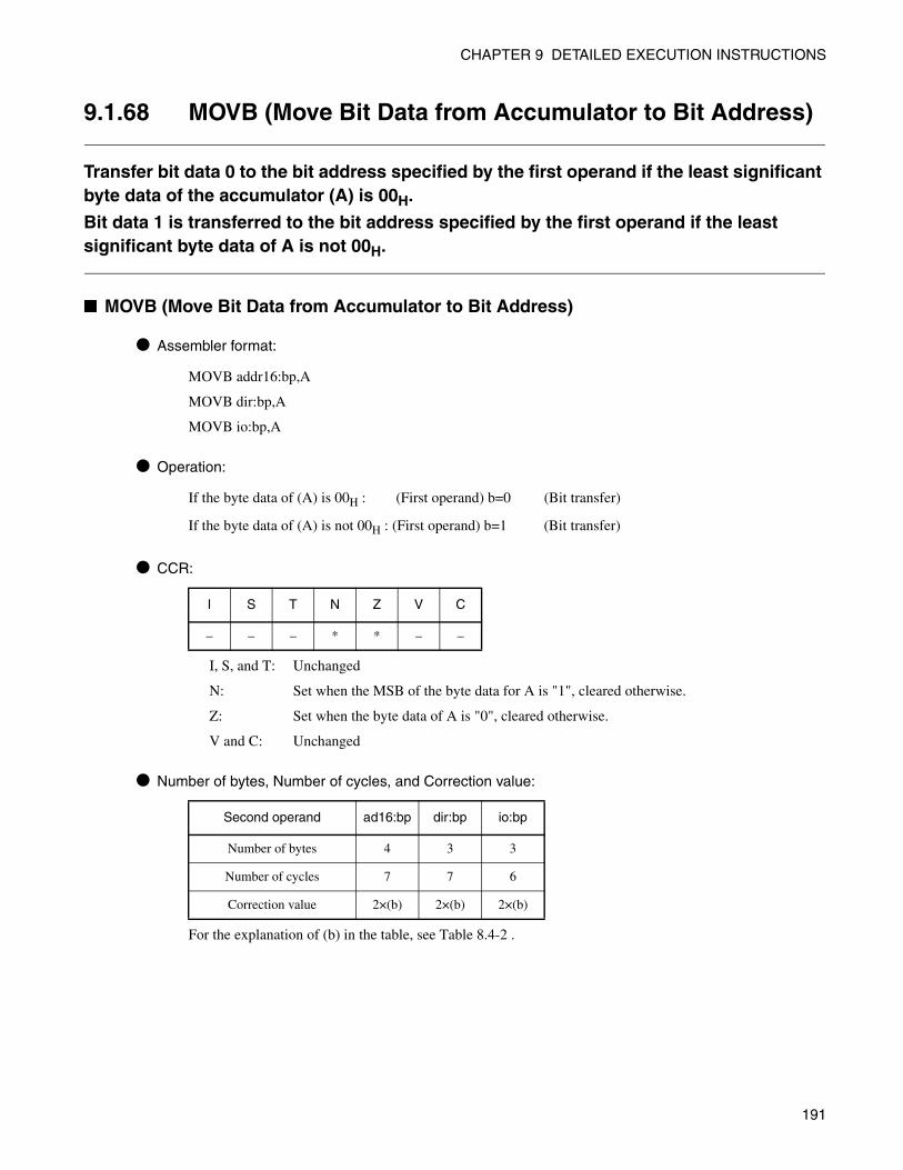
CHAPTER 9 DETAILED EXECUTION INSTRUCTIONS
9.1.68 MOVB (Move Bit Data from Accumulator to Bit Address)
Transfer bit data 0 to the bit address specified by the first operand if the least significant byte data of the accumulator (A) is 00H.
Bit data 1 is transferred to the bit address specified by the first operand if the least significant byte data of A is not 00H.
■ MOVB (Move Bit Data from Accumulator to Bit Address)
● Assembler format:
MOVB addr16:bp,A
MOVB dir:bp,A
MOVB io:bp,A
● Operation:
If the byte data of (A) is 00H : (First operand) b=0 (Bit transfer)
If the byte data of (A) is not 00H : (First operand) b=1 (Bit transfer)
● CCR:
I, S, and T: Unchanged
N: Set when the MSB of the byte data for A is "1", cleared otherwise.
Z: Set when the byte data of A is "0", cleared otherwise.
V and C: Unchanged
● Number of bytes, Number of cycles, and Correction value:
For the explanation of (b) in the table, see Table 8.4-2 .
I S T N Z V C
– – – * * – –
Second operand ad16:bp dir:bp io:bp
Number of bytes 4 3 3
Number of cycles 7 7 6
Correction value 2×(b) 2×(b) 2×(b)
191

CHAPTER 9 DETAILED EXECUTION INSTRUCTIONS
● Example:
MOVB 765FH: 7,A
× × × × × × 0 1 A
Before execution
× × × × × × 0 1 A
After execution
Memory
× ×7 F 765F× ×
Memory
× ×F F 765F× ×
CCR × × × × ×T N Z V C
CCR × 0 0 × ×T N Z V C
192

CHAPTER 9 DETAILED EXECUTION INSTRUCTIONS
9.1.69 MOVEA (Move Effective Address to Destination)
Transfer the value specified by the second operand (effective address) to the first operand. If a general-purpose register is specified by the second operand, the address of the general-purpose register is transferred. If the destination (first operand) is the accumulator (A), the pre-transfer values of bits 0 to 15 are transferred to bits 16 to 31 of A.
■ MOVEA (Move Effective Address to Destination)
● Assembler format:
MOVEA <destination>,ear MOVEA <destination>,eam
● Operation:
First operand ← ea (Word transfer)
● CCR:
None of the flags is changed.
● Number of bytes, Number of cycles, and Correction value:
For the explanation of (a) in the table, see Table 8.4-1 .
● Example:
MOVEA RW2,@RW0+2
I S T N Z V C
– – – – – – –
First operand A A RWi RWi
Second operand ear eam ear eam
Number of bytes 2 2+ 2 2+
Number of cycles 1 1+(a) 3 2+(a)
Correction value 0 0 0 0
Before execution
× × × ×RW2
After execution
0 0 6 BRW2
0 0 6 9RW0 0 0 6 9RW0
CCR × × × × ×T N Z V C
CCR × × × × ×T N Z V C
193

CHAPTER 9 DETAILED EXECUTION INSTRUCTIONS
9.1.70 MOVL (Move Long Word Data from Source to Accumulator)
Transfer the long word data specified by the second operand to the accumulator (A).
■ MOVL (Move Long Word Data from Source to Accumulator)
● Assembler format:
MOVL A,#imm32
MOVL A,ear MOVL A,eam
● Operation:
(A) ← (Second operand) (Long word transfer)
● CCR:
I, S, and T: Unchanged
N: Set when the MSB of the transferred data is "1", cleared otherwise.
Z: Set when the transferred data is "0", cleared otherwise.
V and C: Unchanged
● Number of bytes, Number of cycles, and Correction value:
For the explanation of (a) and (d) in the table, see Table 8.4-1 and Table 8.4-2 .
● Example:
MOVL A,#0053FF64H
I S T N Z V C
– – – * * – –
Second operand #i32 ear eam
Number of bytes 5 2 2+
Number of cycles 3 4 5+(a)
Correction value 0 0 (d)
× × × × × × × ×A
Before execution
0 0 5 3 F F 6 4A
After execution
CCR × × × × ×T N Z V C
CCR × 0 0 × ×T N Z V C
194

CHAPTER 9 DETAILED EXECUTION INSTRUCTIONS
9.1.71 MOVL (Move Long Word Data from Accumulator to Destination)
Transfer the long word data of the accumulator (A) to the first operand.
■ MOVL (Move Long Word Data from Accumulator to Destination)
● Assembler format:
MOVL ear,A MOVL eam,A
● Operation:
(First operand) ← (A) (Long word transfer)
● CCR:
I, S, and T: Unchanged
N: Set when the MSB of the transferred data is "1", cleared otherwise.
Z: Set when the transferred data is "0", cleared otherwise.
V and C: Unchanged
● Number of bytes, Number of cycles, and Correction value:
For the explanation of (a) and (d) in the table, see Table 8.4-1 and Table 8.4-2 .
● Example:
MOVL RL1,A
I S T N Z V C
– – – * * – –
First operand ear eam
Number of bytes 2 2+
Number of cycles 4 5+(a)
Correction value 0 (d)
Before execution After execution
0 1 9 7 A 0 2 4A 0 1 9 7 A 0 2 4A
× × × × × × × ×RL1 0 1 9 7 A 0 2 4RL1
CCR × × × × ×T N Z V C
CCR × 0 0 × ×T N Z V C
195

CHAPTER 9 DETAILED EXECUTION INSTRUCTIONS
9.1.72 MOVN (Move Immediate Nibble Data to Accumulator)
Transfer the values of bits 0 to 15 for the accumulator (A) to bits 16 to 31. "0" is transferred to bits 4 to 15 and the nibble data specified by the second operand is transferred to bits 0 to 3.
■ MOVN (Move Immediate Nibble Data to Accumulator)
● Assembler format:
MOVN A,#imm4
● Operation:
(A) ← imm4 (Byte transfer)
● CCR:
I, S, and T: Unchanged
N: Cleared
Z: Set when the transferred data is "0", cleared otherwise.
V and C: Unchanged
● Number of bytes, Number of cycles, and Correction value:
Number of bytes: 1
Number of cycles: 1
Correction value: 0
● Example:
MOVN A,#0FH
I S T N Z V C
– – – R * – –
× × × × 6 2 0 7 A
Before execution
6 2 0 7 0 0 0 F A
After execution
CCR × × × × ×T N Z V C
CCR × 0 0 × ×T N Z V C
196

CHAPTER 9 DETAILED EXECUTION INSTRUCTIONS
9.1.73 MOVS (Move String Byte)
Transfer byte data from the address specified by AL in the space specified by <source bank> to the address specified by AH in the space specified by <destination bank>. The transfer is repeated the number of times specified by RW0, with the addresses being changed each time. The transfer is not performed if RW0 is equal to "0". Four types of registers PCB, DTB, ADB, and SPB can be used as <destination bank> and <source bank>. By default, DTB is assumed. The addresses can be either incremented or decremented. By default, the addresses are incremented. If an interrupt occurs during the transfer, the transfer is suspended to handle the interrupt. The transfer is resumed after the interrupt has been handled.
■ MOVS (Move String Byte)
● Assembler format:
MOVSI [<destination bank>] [,<source bank>] (When the addresses are incremented)
MOVSD [<destination bank>] [,<source bank>] (When the addresses are decremented)
● Operation:
The following is repeated until RW0 becomes equal to "0":
((AH)) ← ((AL)) (Byte transfer)
(AH) ← (AH)±1, (AL) ← (AL)±1 (+ if MOVSWI, – if MOVSWD)
(RW0) ← (RW0)–1
● CCR:
None of the flags is changed.
● Number of bytes, Number of cycles, and Correction value:
Number of bytes: 2
Number of cycles: 5 if (RW0) is equal to "0"; otherwise, 4+8×(RW0)
Correction value: 2×(b)×(RW0)
For the explanation of (b), see Table 8.4-2 .
I S T N Z V C
– – – – – – –
197

CHAPTER 9 DETAILED EXECUTION INSTRUCTIONS
● Example:
MOVSI ADB,PCB
0 0 0 3RW0
Before execution
Memory
F C FF0003F D FF0002F E FF0001
F FPCB
× × 018002× × 018001
AH
8 0 0 0 0 0 0 0 AH AL
× × 018000
0 1ADB
F F FF0000AL
× × 018003
0 0 0 0RW0
After execution
Memory
F C FF0003F D FF0002F E FF0001
F FPCB
F D 018002F E 018001
AH
AH AL
F F 018000
0 1ADB
F F FF0000
AL
× × 018003
8 0 0 3 0 0 0 3
CCR × × × × ×T N Z V C
CCR × × × × ×T N Z V C
198
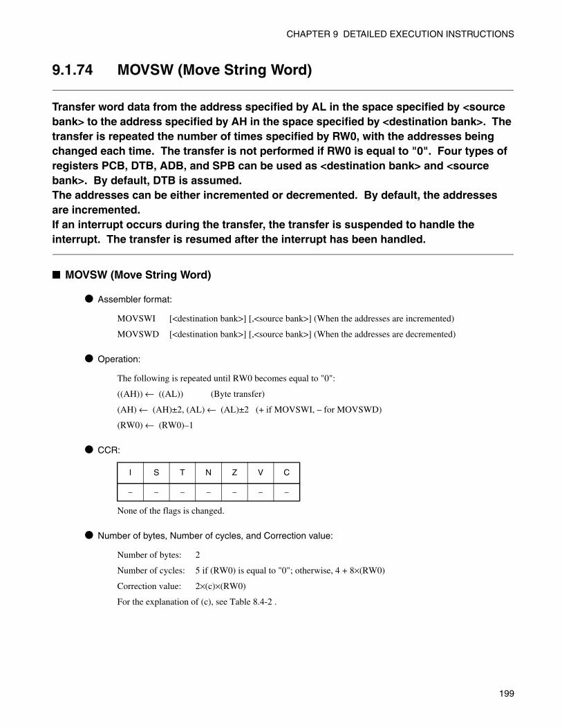
CHAPTER 9 DETAILED EXECUTION INSTRUCTIONS
9.1.74 MOVSW (Move String Word)
Transfer word data from the address specified by AL in the space specified by <source bank> to the address specified by AH in the space specified by <destination bank>. The transfer is repeated the number of times specified by RW0, with the addresses being changed each time. The transfer is not performed if RW0 is equal to "0". Four types of registers PCB, DTB, ADB, and SPB can be used as <destination bank> and <source bank>. By default, DTB is assumed. The addresses can be either incremented or decremented. By default, the addresses are incremented. If an interrupt occurs during the transfer, the transfer is suspended to handle the interrupt. The transfer is resumed after the interrupt has been handled.
■ MOVSW (Move String Word)
● Assembler format:
MOVSWI [<destination bank>] [,<source bank>] (When the addresses are incremented)
MOVSWD [<destination bank>] [,<source bank>] (When the addresses are decremented)
● Operation:
The following is repeated until RW0 becomes equal to "0":
((AH)) ← ((AL)) (Byte transfer)
(AH) ← (AH)±2, (AL) ← (AL)±2 (+ if MOVSWI, – for MOVSWD)
(RW0) ← (RW0)–1
● CCR:
None of the flags is changed.
● Number of bytes, Number of cycles, and Correction value:
Number of bytes: 2
Number of cycles: 5 if (RW0) is equal to "0"; otherwise, 4 + 8×(RW0)
Correction value: 2×(c)×(RW0)
For the explanation of (c), see Table 8.4-2 .
I S T N Z V C
– – – – – – –
199

CHAPTER 9 DETAILED EXECUTION INSTRUCTIONS
● Example:
MOVSW,ADB
0 0 0 3RW0
Before execution
Memory
× × CD0005× × CD0004× × CD0003
C DDTB
3 1 38A0024 D 38A001
AL
AH AL
4 6 38A000
3 8ADB
× × CD0002
AH
3 6 38A003
0 0 0 0RW0
After execution
Memory
2 6 CD00054 2 CD00043 6 CD0003
C DDTB
3 1 38A0024 D 38A001
AL
AH AL
4 6 38A000
3 8ADB
3 1 CD0002
AH
3 6 38A0034 2 38A0042 6 38A005
4 2 38A0042 6 38A005
× × CD0001× × CD0000
4 D CD00014 6 CD0000
0 0 0 0 A 0 0 0 0 0 0 6 A 0 0 6
CCR × × × × ×T N Z V C
CCR × × × × ×T N Z V C
200

CHAPTER 9 DETAILED EXECUTION INSTRUCTIONS
9.1.75 MOVW (Move Word Data from Source to Accumulator)
Transfer the values of bits 0 to 15 for the accumulator (A) to bits 16 to 31. Then, the word data specified by the second operand is transferred to bit0 to bit15 of A. If the second operand is @A, transfer the values of bits 0 to 15 of A to bits 16 to 31 is not performed.
■ MOVW (Move Word Data from Source to Accumulator)
● Assembler format:
MOVW A,#imm16 MOVW A,@RWi+disp8
MOVW A,@A MOVW A,addr16
MOVW A,@RLi+disp8 MOVW A,RWi
MOVW A,SP MOVW A,dir
MOVW A,io
MOVW A,ear MOVW A,eam
● Operation:
(A) ← (Second operand) (Word transfer)
● CCR:
I, S, and T: Unchanged
N: Set when the MSB of the transferred data is "1", cleared otherwise.
Z: Set when the transferred data is "0", cleared otherwise.
V and C: Unchanged
● Number of bytes, Number of cycles, and Correction value:
For the explanation of (a) and (c) in the table, see Table 8.4-1 and Table 8.4-2 .
I S T N Z V C
– – – * * – –
Second operand #i16 @A @RLi+8 SP io @RWi+8 ad16 RWi dir ear eam
Number of bytes 3 2 3 1 2 2 3 1 2 2 2+
Number of cycles 2 3 10 1 3 5 4 2 3 2 3+(a)
Correction value 0 (c) (c) 0 (c) (c) (c) 0 (c) 0 (c)
201

CHAPTER 9 DETAILED EXECUTION INSTRUCTIONS
● Example:
MOVW A,0F9A0H
× × × × 4 9 0 1 A
Before execution
4 9 0 1 A E 8 6 A
After execution
Memory Memory
A E F9A1 A E F9A18 6 F9A0 8 6 F9A0
CCR × × × × ×T N Z V C
CCR × 1 0 × ×T N Z V C
202

CHAPTER 9 DETAILED EXECUTION INSTRUCTIONS
9.1.76 MOVW (Move Word Data from Accumulator to Destination)
Transfer the low-order word data of the accumulator (A) to the first operand.
■ MOVW (Move Word Data from Accumulator to Destination)
● Assembler format:
MOVW @RLi+disp8,A MOVW addr16,A
MOVW SP,A MOVW RWi,A
MOVW io,A MOVW dir,A
MOVW @RWi+disp8,A
MOVW ear,A MOVW eam,A
● Operation:
(First operand) ← (A) (Word transfer)
● CCR:
I, S, and T: Unchanged
N: Set when the MSB of the transferred data is "1", cleared otherwise.
Z: Set when the transferred data is "0", cleared otherwise.
V and C: Unchanged
● Number of bytes, Number of cycles, and Correction value:
For the explanation of (a) and (c) in the table, see Table 8.4-1 and Table 8.4-2 .
I S T N Z V C
– – – * * – –
First operand dir @RLi+8 ad16 SP io @RWi+8 RWi ear eam
Number of bytes 2 3 3 1 2 2 1 2 2+
Number of cycles 3 10 4 1 3 5 2 2 3+(a)
Correction value (c) (c) (c) 0 (c) (c) 0 0 (c)
203

CHAPTER 9 DETAILED EXECUTION INSTRUCTIONS
● Example:
MOVW RW0,A
× × × × 0 0 0 0A
Before execution
× × × ×RW0
× × × × 0 0 0 0A
After execution
0 0 0 0RW0
CCR × × × × ×T N Z V C
CCR × 0 1 × ×T N Z V C
204

CHAPTER 9 DETAILED EXECUTION INSTRUCTIONS
9.1.77 MOVW (Move Immediate Word Data to Destination)
This instruction transfers the 16-bit immediate data to the first operand.When the first operand is @PC + disp16, the transfer destination address is the address where the machine instruction of the MOVW instruction is stored + 4 + disp16. Note that this is not the address where the machine instruction of the instruction subsequent to the MOVW instruction is stored+disp16.
■ MOVW (Move Immediate Word Data to Destination)
● Assembler format:
MOVW ear,#imm16 MOVW eam,#imm16
● Operation:
(First operand) ← #imm16
● CCR:
If the data is transferred to a general- If the data is transferred to a register
purpose register (RW0 to RW7) other than the general-purpose registers
(RW0 to RW7)
I, S, and T: Unchanged
N: Unchanged if the data is transferred to a register other than the general-purpose registers.
If the data is transferred to the general-purpose register, N is set when the MSB of the
transferred data is "1", cleared otherwise.
Z: Unchanged if the data is transferred to a register other than the general-purpose registers.
If the data is transferred to the general-purpose register, Z is set when the transferred data
is "0", cleared otherwise.
V and C: Unchanged and none of the flags is changed.
● Number of bytes, Number of cycles, and Correction value:
For the explanation of (a) and (c) in the table, see Table 8.4-1 and Table 8.4-2 .
I S T N Z V C I S T N Z V C
– – – * * – – – – – – – – –
First operand ear eam
Number of bytes 4 4+
Number of cycles 2 4+(a)
Correction value 0 (c)
205

CHAPTER 9 DETAILED EXECUTION INSTRUCTIONS
● Example:
MOVW RW0,#2343H
Before execution
× × × ×RW0
After execution
2 3 4 3RW0
CCR × × × × ×T N Z V C
CCR × 0 0 × ×T N Z V C
206

CHAPTER 9 DETAILED EXECUTION INSTRUCTIONS
9.1.78 MOVW (Move Word Data from Source to Destination)
Transfer the word data specified by the second operand to the first operand.
■ MOVW (Move Word Data from Source to Destination)
● Assembler format:
MOVW RWi,#imm16
MOVW ear,RWi MOVW eam,RWi
MOVW RWi,ear MOVW RWi,eam
● Operation:
(First operand) ← (Second operand) (Word transfer)
● CCR:
I, S, and T: Unchanged
N: Set when the MSB of the transferred data is "1", cleared otherwise.
Z: Set when the transferred data is "0", cleared otherwise.
V and C: Unchanged
● Number of bytes, Number of cycles, and Correction value:
For the explanation of (a) and (c) in the table, see Table 8.4-1 and Table 8.4-2 .
I S T N Z V C
– – – * * – –
First operand RWi RWi RWi ear eam
Second operand #i16 ear eam RWi RWi
Number of bytes 3 2 2+ 2 2+
Number of cycles 2 4 5+(a) 3 4+(a)
Correction value 0 0 (c) 0 (c)
207

CHAPTER 9 DETAILED EXECUTION INSTRUCTIONS
● Example:
MOVW RW1,RW0
Before execution
0 0 4 ARW0
After execution
0 0 4 ARW0
× × × × RW1 0 0 4 A RW1
× × × × × × × × A × × × × × × × × A
CCR × × × × ×T N Z V C
CCR × 0 0 × ×T N Z V C
208

CHAPTER 9 DETAILED EXECUTION INSTRUCTIONS
9.1.79 MOVW (Move Immediate Word Data to io)
Transfer 16-bit immediate data to the I/O area specified by the first operand.
■ MOVW (Move Immediate Word Data to io)
● Assembler format:
MOVW io,#imm16
● Operation:
(First operand) ← imm16 (Word transfer)
● CCR:
None of the flags is changed.
● Number of bytes, Number of cycles, and Correction value:
Number of bytes: 4
Number of cycles: 5
Correction value: (c)
For the explanation of (c), see Table 8.4-2 .
● Example:
MOVW 24H,#2343H
I S T N Z V C
– – – – – – –
Before execution After execution
Memory
× ×
Memory
× ×× × 000025 2 3 000025× × 000024 4 3 000024× × × ×
CCR × × × × ×T N Z V C
CCR × × × × ×T N Z V C
209

CHAPTER 9 DETAILED EXECUTION INSTRUCTIONS
9.1.80 MOVW (Move Word Data from AH to Memory)
Transfer the word data of AH to the memory location specified by the contents of AL.
■ MOVW (Move Word Data from AH to Memory)
● Assembler format:
MOVW @AL,AH
● Operation:
((AL)) ← (AH) (Word transfer)
● CCR:
I, S, and T: Unchanged
N: Set when the MSB of the transferred data is "1", cleared otherwise.
Z: Set when the transferred data is "0", cleared otherwise.
V and C: Unchanged
● Number of bytes, Number of cycles, and Correction value:
Number of bytes: 2
Number of cycles: 3
Correction value: (c)
For the explanation of (c), see Table 8.4-2 .
● Example:
MOVW @AL,AH
I S T N Z V C
– – – * * – –
0 0 C B F E F F A
Before execution
0 0 C B F E F F A
After execution
Memory Memory
7 1 FEFF C B FEFF
CCR × × × × ×T N Z V C
CCR × 1 0 × ×T N Z V C
210

CHAPTER 9 DETAILED EXECUTION INSTRUCTIONS
9.1.81 MOVX (Move Byte Data with Sign Extension from Source to Accumulator)
Transfer the values of bits 0 to 15 for the accumulator (A) to bits 16 to 31. Then, the value resulting from sign-extending the second operand is transferred to bits 0 to 15 of A. If the second operand is @A, transfer to bits 16 to 31 is not performed.
■ MOVX (Move Byte Data with Sign Extension from Source to Accumulator)
● Assembler format:
MOVX A,#imm8 MOVX A,@RWi+disp8
MOVX A,@A MOVX A,addr16
MOVX A,@RLi+disp8 MOVX A,Ri
MOVX A,dir MOVX A,io
MOVX A,ear MOVX A,eam
● Operation:
(A) ← (Second operand) (Byte transfer with sign extension)
● CCR:
I, S, and T: Unchanged
N: Set when the MSB of the transferred data is "1", cleared otherwise.
Z: Set when the transferred data is "0", cleared otherwise.
V and C: Unchanged
● Number of bytes, Number of cycles, and Correction value:
For the explanation of (a) and (b) in the table, see Table 8.4-1 and Table 8.4-2 .
I S T N Z V C
– – – * * – –
Second operand #im8 @A @RLi+8 dir io @RWi+8 ad16 Ri ear eam
Number of bytes 2 2 3 2 2 2 3 2 2 2+
Number of cycles 2 3 10 3 3 5 4 2 2 3+(a)
Correction value 0 (b) (b) (b) (b) (b) (b) 0 0 (b)
211

CHAPTER 9 DETAILED EXECUTION INSTRUCTIONS
● Example:
MOVX A,0E001H
× × × × A 0 4 6 A
Before execution
A 0 4 6 F F 8 6 A
After execution
Memory Memory
8 6 E001 8 6 E001
CCR × × × × ×T N Z V C
CCR × 1 0 × ×T N Z V C
212

CHAPTER 9 DETAILED EXECUTION INSTRUCTIONS
9.1.82 MUL (Multiply Byte Data of Accumulator)
This instruction multiplies the low-order byte data of AH by that of AL as signed binary numbers, then returns the result to AL of the accumulator (A).
■ MUL (Multiply Byte Data of Accumulator)
● Assembler format:
MUL A
● Operation:
word (A) ← byte (AH)×byte (AL) (Byte multiplication)
● CCR:
None of the flags is changed.
● Number of bytes, Number of cycles, and Correction value:
Number of bytes: 2
Number of cycles: 3 if byte (AH) is equal to "0"; 12 if byte (AH) is not equal to "0" and the result is
positive; 13 if the result is negative.
Correction value: 0
● Example:
MUL A
I S T N Z V C
– – – – – – –
Before execution After execution
AH AL AH AL
0 0 F A 0 0 1 1 A 0 0 F A F F 9 A A
CCR × × × × ×T N Z V C
CCR × × × × ×T N Z V C
213

CHAPTER 9 DETAILED EXECUTION INSTRUCTIONS
9.1.83 MUL (Multiply Byte Data of Accumulator and Effective Address)
Multiply the byte data of the accumulator (A) by the byte data specified by the second operand as signed binary numbers and restore the result in bits 0 to 15 of A.
■ MUL (Multiply Byte Data of Accumulator and Effective Address)
● Assembler format:
MUL A,ear MUL A,eam
● Operation:
word (A) ← byte (A) × byte (ea) (Byte multiplication)
● CCR:
None of the flags is changed.
● Number of bytes, Number of cycles, and Correction value:
*1: 4 if byte (ear) is equal to "0"; 13 if byte (ear) is not equal to"0" and the result is positive; 14 if the result is negative. *2: 5 + (a) if byte (eam) is equal to "0"; 14 + (a) if byte (eam) is not equal to "0" and the result is positive; 15 + (a) if the
result is negative.
For the explanation of (b) in the table and (a) in *2, see Table 8.4-1 and Table 8.4-2 .
● Example:
MUL A,R7
I S T N Z V C
– – – – – – –
Second operand ear eam
Number of bytes 2 2+
Number of cycles *1 *2
Correction value 0 (b)
× × × × 0 0 8 5A
Before execution
× × × × 2 B B 9 A
After execution
A 5R7 A 5R7
AH AL AH AL
CCR × × × × ×T N Z V C
CCR × × × × ×T N Z V C
214

CHAPTER 9 DETAILED EXECUTION INSTRUCTIONS
9.1.84 MULW (Multiply Word Data of Accumulator)
Multiply the word data of AH by the word data specified by AL as signed binary numbers and restore the result in the accumulator as long word data.
■ MULW (Multiply Word Data of Accumulator)
● Assembler format:
MULW A
● Operation:
Long (A) ← word (AH)×word (AL) (Word multiplication)
● CCR:
None of the flags is changed.
● Number of bytes, Number of cycles, and Correction value:
Number of bytes: 2
Number of cycles: 3 if word (AH) is equal to "0"; 16 if word (AH) is not equal to "0" and the result is
positive; 19 if the result is negative.
Correction value: 0
● Example:
MULW A
I S T N Z V C
– – – – – – –
A D 0 1 0 5 E D A
Before execution After execution
AH AL AH AL
F E 1 4 2 E E D A
CCR × × × × ×T N Z V C
CCR × × × × ×T N Z V C
215

CHAPTER 9 DETAILED EXECUTION INSTRUCTIONS
9.1.85 MULW (Multiply Word Data of Accumulator and Effective Address)
Multiply the word data of the accumulator (A) by the word data specified by the second operand as signed binary numbers and restore the result in A as long word data.
■ MULW (Multiply Word Data of Accumulator and Effective Address)
● Assembler format:
MULW A,ear MULW A,eam
● Operation:
Long (A) ← word (A)×word (Second operand) (Word multiplication)
● CCR:
None of the flags is changed.
● Number of bytes, Number of cycles, and Correction value:
*1: 4 if Word (ear) is equal to "0"; 17 if Word (ear) is not equal to "0" and the result is positive; 20 if the result is negative.
*2: 5 + (a) if Word (eam) is equal to "0"; 18 + (a) if Word (eam) is not equal to "0" and the result is positive; 21 + (a) if the result is negative.
For the explanation of (b) in the table and (a) in *2, see Table 8.4-1 and Table 8.4-2 .
● Example:
MULW A,RW5
I S T N Z V C
– – – – – – –
Second operand ear eam
Number of bytes 2 2+
Number of cycles *1 *2
Correction value 0 (b)
Before execution After execution
AH AL AH AL
4 3 1 4 RW5 4 3 1 4RW5
× × × × 8 3 4 2 A D F 5 0 8 7 2 8 A
CCR × × × × ×T N Z V C
CCR × × × × ×T N Z V C
216

CHAPTER 9 DETAILED EXECUTION INSTRUCTIONS
9.1.86 MULU (Multiply Unsigned Byte Data of Accumulator)
Multiply the low-order byte data of AH by the low-order byte data of AL as unsigned binary numbers and restore the result in the AL of the accumulator (A).
■ MULU (Multiply Unsigned Byte Data of Accumulator)
● Assembler format:
MULU A
● Operation:
word (A) ← byte (AH)×byte (AL) (Byte multiplication)
● CCR:
None of the flags is changed.
● Number of bytes, Number of cycles, and Correction value:
Number of bytes: 1
Number of cycles: 3 if byte (AH) is equal to "0"; 7 if byte (AH) is not equal to "0".
Correction value: 0
● Example:
MULU A
I S T N Z V C
– – – – – – –
Before execution After execution
0 0 F A 0 0 1 1 A 0 0 F A 1 0 9 A A
CCR × × × × ×T N Z V C
CCR × × × × ×T N Z V C
217

CHAPTER 9 DETAILED EXECUTION INSTRUCTIONS
9.1.87 MULU (Multiply Unsigned Byte Data of Accumulator and Effective Address)
Multiply the byte data of the accumulator (A) by the byte data specified by the second operand as unsigned binary numbers and restore the result in bits 0 to 15 of A.
■ MULU (Multiply Unsigned Byte Data of Accumulator and Effective Address)
● Assembler format:
MULU A, ear MULU A, eam
● Operation:
word (A) ← byte (A) × byte (Second operand) (Byte multiplication)
● CCR:
None of the flags is changed.
● Number of bytes, Number of cycles, and Correction value:
*1: 4 if byte (ear) is equal to "0"; 8 if byte (ear) is not equal to "0". *2: 5 + (a) if byte (eam) is equal to "0"; 9 + (a) if not equal to "0".
For the explanation of (b) in the table and (a) in *2, see Table 8.4-1 and Table 8.4-2 .
● Example:
MULU A, R7
I S T N Z V C
– – – – – – –
Second operand ear eam
Number of bytes 2 2 +
Number of cycles *1 *2
Correction value 0 (b)
Before execution After execution
R7 R7A 5 A 5
× × × × 0 0 8 5 A × × × × 5 5 B 9 A
CCR × × × × ×T N Z V C
CCR × × × × ×T N Z V C
218

CHAPTER 9 DETAILED EXECUTION INSTRUCTIONS
9.1.88 MULUW (Multiply Unsigned Word Data of Accumulator)
Multiply the word data of AH by the word data of AL as unsigned binary numbers and restore the result in the accumulator (A) as long word data.
■ MULUW (Multiply Unsigned Word Data of Accumulator)
● Assembler format:
MULUW A
● Operation:
Long (A) ← word (AH)×word (AL) (Word multiplication)
● CCR:
None of the flags is changed.
● Number of bytes, Number of cycles, and Correction value:
Number of bytes: 1
Number of cycles: 3 if word (AH) is equal to "0"; 11 if word (AH) is not equal to "0".
Correction value: 0
● Example:
MULUW A
I S T N Z V C
– – – – – – –
Before execution After execution
A D 0 1 0 5 E D A 0 4 0 1 2 E E D A
CCR × × × × ×T N Z V C
CCR × × × × ×T N Z V C
219

CHAPTER 9 DETAILED EXECUTION INSTRUCTIONS
9.1.89 MULUW (Multiply Unsigned Word Data of Accumulator and Effective Address)
Multiply the word data of the accumulator (A) by the word data specified by the second operand as unsigned binary numbers and restore the result in A as long word data.
■ MULUW (Multiply Unsigned Word Data of Accumulator and Effective Address)
● Assembler format:
MULUW A, ear MULUW A, eam
● Operation:
Long (A) ← word (A)×word (Second operand) (Word multiplication)
● CCR:
None of the flags is changed.
● Number of bytes, Number of cycles, and Correction value:
*1: 4 if Word (ear) is equal to "0"; 12 if Word (ear) is not equal to "0". *2: 5 + (a) if Word (eam) is "0"; 13 + (a) if Word (eam) is not equal to "0".
For the explanation of (c) in the table and (a) in *2, see Table 8.4-1 and Table 8.4-2 .
● Example:
MULUW A, RW5
I S T N Z V C
– – – – – – –
Second operand ear eam
Number of bytes 2 2+
Number of cycles *1 *2
Correction value 0 (c)
4 3 1 4RW5
Before execution
× × × × 8 3 4 2 A
4 3 1 4RW5
After execution
A 2 2 6 4 8 7 2 8
CCR × × × × ×T N Z V C
CCR × × × × ×T N Z V C
220

CHAPTER 9 DETAILED EXECUTION INSTRUCTIONS
9.1.90 NEG (Negate Byte Data of Destination)
Take the 2's complement of the byte data specified by the operand and restore the result in the operand. If the operand is the accumulator (A), the value resulting from sign-extending the operation result is transferred to bits 8 to 15 of A.
■ NEG (Negate Byte Data of Destination)
● Assembler format:
NEG A
NEG ear NEG eam
● Operation:
(Operand) ← 0–(Operand) (Byte operation)
● CCR:
I, S, and T: Unchanged
N: Set when the MSB of the operation result is "1", cleared otherwise.
Z: Set when the operation result is "0", cleared otherwise.
V: Set when an overflow has occurred as a result of the operation, cleared otherwise.
C: Set when a borrow has occurred as a result of the operation, cleared otherwise.
● Number of bytes, Number of cycles, and Correction value:
For the explanation of (a) and (b) in the table, see Table 8.4-1 and Table 8.4-2 .
● Example:
NEG R0
I S T N Z V C
– – – * * * *
Operand A ear eam
Number of bytes 1 2 2+
Number of cycles 2 3 5+(a)
Correction value 0 0 2×(b)
Before execution After execution
5 9R0 A 7R0
CCR × × × × ×T N Z V C
CCR × 1 0 0 1
T N Z V C
221

CHAPTER 9 DETAILED EXECUTION INSTRUCTIONS
9.1.91 NEGW (Negate Word Data of Destination)
Take the 2's complement of the word data specified by the operand and restore the result in the operand.
■ NEGW (Negate Word Data of Destination)
● Assembler format:
NEGW A
NEGW ear NEGW eam
● Operation:
(Operand) ← 0–(Operand) (Word operation)
● CCR:
I, S, and T: Unchanged
N: Set when the MSB of the operation result is "1", cleared otherwise.
Z: Set when the operation result is "0", cleared otherwise.
V: Set when an overflow has occurred as a result of the operation, cleared otherwise.
C: Set when a borrow has occurred as a result of the operation, cleared otherwise.
● Number of bytes, Number of cycles, and Correction value:
For the explanation of (a) and (c) in the table, see Table 8.4-1 and Table 8.4-2 .
● Example:
NEGW A
I S T N Z V C
– – – * * * *
Operand A ear eam
Number of bytes 1 2 2+
Number of cycles 2 3 5+(a)
Correction value 0 0 2×(c)
× × × × A B 9 8 A
Before execution
× × × × 5 4 6 8 A
After execution
CCR × × × × ×T N Z V C
CCR × 0 0 0 1
T N Z V C
222

CHAPTER 9 DETAILED EXECUTION INSTRUCTIONS
9.1.92 NOP (No Operation)
Perform no operation.
■ NOP (No Operation)
● Assembler format:
NOP
● Operation:
No operation is performed.
● CCR:
None of the flags is changed.
● Number of bytes, Number of cycles, and Correction value:
Number of bytes: 1
Number of cycles: 1
Correction value: 0
● Example:
NOP
I S T N Z V C
– – – – – – –
× × × × × × × × A
F 0 0 0 PC
× × × × × × × × A
F 0 0 1 PC
Before execution After execution
Memory Memory
× × F001 × × F0010 0 F000 0 0 F000PC
PC
CCR × × × × ×T N Z V C
CCR × × × × ×T N Z V C
223

CHAPTER 9 DETAILED EXECUTION INSTRUCTIONS
9.1.93 NOT (Not Byte Data of Destination)
Take the logical NOT of the byte data specified by the operand and restore the result in the operand.
■ NOT (Not Byte Data of Destination)
● Assembler format:
NOT A
NOT ear NOT eam
● Operation:
(Operand) ← not (Operand) (Byte logical NOT)
● CCR:
I, S, and T: Unchanged
N: Set when the MSB of the operation result is "1", cleared otherwise.
Z: Set when the operation result is "0", cleared otherwise.
V: Cleared
C: Unchanged
● Number of bytes, Number of cycles, and Correction value:
For the explanation of (a) and (b) in the table, see Table 8.4-1 and Table 8.4-2 .
I S T N Z V C
– – – * * R –
Operand A ear eam
Number of bytes 1 2 2+
Number of cycles 2 3 5+(a)
Correction value 0 0 2×(b)
224

CHAPTER 9 DETAILED EXECUTION INSTRUCTIONS
● Example:
NOT 0071H
× × × × × × × × A
Before execution
× × × × × × × × A
After execution
Memory Memory
F F 0071 0 0 0071
CCR × × × × ×T N Z V C
CCR × 0 1 0 ×T N Z V C
225

CHAPTER 9 DETAILED EXECUTION INSTRUCTIONS
9.1.94 NOTW (Not Word Data of Destination)
Take the logical NOT of the word data specified by the operand and restore the result in the operand.
■ NOTW (Not Word Data of Destination)
● Assembler format:
NOTW A
NOTW ear NOTW eam
● Operation:
(Operand) ← not (Operand) (Word logical NOT)
● CCR:
I, S, and T: Unchanged
N: Set when the MSB of the operation result is "1", cleared otherwise.
Z: Set when the operation result is "0", cleared otherwise.
V: Cleared
C: Unchanged
● Number of bytes, Number of cycles, and Correction value:
For the explanation of (a) and (c) in the table, see Table 8.4-1 and Table 8.4-2 .
● Example:
NOTW RW3
I S T N Z V C
– – – * * R –
Operand A ear eam
Number of bytes 1 2 2+
Number of cycles 2 3 5+(a)
Correction value 0 0 2×(c)
Before execution
2 5 8 B RW3
After execution
D A 7 4 RW3
CCR × × × × ×T N Z V C
CCR × 1 0 0 ×T N Z V C
226

CHAPTER 9 DETAILED EXECUTION INSTRUCTIONS
9.1.95 NRML (NORMALIZE Long Word)
Shift the long word data of the accumulator (A) to the left until the most significant bit of A becomes "1", if the long word data is not "0". R0 is set to the number of shifts required and the zero flag (Z) is cleared. If the long word data of the accumulator (A) is "0", R0 is set to "0" and the zero flag (Z) is set.
■ NRML (NORMALIZE Long Word)
● Assembler format:
NRML A,R0
● Operation:
If A≠0: The long word data is shifted to the left until the most significant bit of A becomes 1.
(R0) ← Number of shifts required, Z ← 0
If A=0: (R0) ← 0, Z ← 1
● CCR:
I, S, T, and N: Unchanged
Z: Set when A is equal to "0", cleared otherwise.
V and C: Unchanged
● Number of bytes, Number of cycles, and Correction value:
Number of bytes: 2
Number of cycles: 4 when the accumulator is equal to "0"; otherwise, 6 + (Number of shifts required)
Correction value: 0
● Example:
NRML A,R0
I S T N Z V C
– – – – * – –
0 0 0 0 8 3 6 1 A
Before execution
8 3 6 1 0 0 0 0A
After execution
3 4R0 1 0R0
CCR × × × × ×T N Z V C
CCR × × 0 × ×T N Z V C
227

CHAPTER 9 DETAILED EXECUTION INSTRUCTIONS
9.1.96 OR (Or Byte Data of Destination and Source to Destination)
Take the logical OR of the byte data specified by the first operand and the byte data specified by the second operand and restore the result in the first operand.
■ OR (Or Byte Data of Destination and Source to Destination)
● Assembler format:
OR A,#imm8
OR A,ear OR A,eam
OR ear,A OR eam,A
● Operation:
(First operand) ← (First operand) or (Second operand) (Byte logical OR)
● CCR:
I, S, and T: Unchanged
N: Set when the MSB of the operation result is "1", cleared otherwise.
Z: Set when the operation result is "0", cleared otherwise.
V: Cleared
C: Unchanged
● Number of bytes, Number of cycles, and Correction value:
For the explanation of (a) and (b) in the table, see Table 8.4-1 and Table 8.4-2 .
I S T N Z V C
– – – * * R –
First operand A A A ear eam
Second operand #im8 ear eam A A
Number of bytes 2 2 2+ 2 2+
Number of cycles 2 3 4+(a) 3 5+(a)
Correction value 0 0 (b) 0 2×(b)
228

CHAPTER 9 DETAILED EXECUTION INSTRUCTIONS
● Example:
OR 0052H,A
× × × × 0 0 3 7 A
Before execution
× × × × 0 0 3 7 A
After execution
Memory Memory
F A 0052 F F 0052
CCR × × × × ×T N Z V C
CCR × 1 0 0 ×T N Z V C
229

CHAPTER 9 DETAILED EXECUTION INSTRUCTIONS
9.1.97 OR (Or Byte Data of Immediate Data and Condition Code Register to Condition Code Register)
Take the logical OR of the byte data in the condition code register (CCR) and specified 8-bit immediate data and restore the result in the condition code register (CCR). Bit 7 of the immediate data is ignored because the condition code register (CCR) is 7 bits long.
■ OR (Or Byte Data of Immediate Data and Condition Code Register to Condition Code Register)
● Assembler format:
OR CCR,#imm8
● Operation:
(CCR) ← (CCR) or #imm8 (Byte logical OR)
● CCR:
I: Stores bit 6 of the operation result.
S: Stores bit 5 of the operation result.
T: Stores bit 4 of the operation result.
N: Stores bit 3 of the operation result.
Z: Stores bit 2 of the operation result.
V: Stores bit 1 of the operation result.
C: Stores bit 0 of the operation result.
● Number of bytes, Number of cycles, and Correction value:
Number of bytes: 2
Number of cycles: 3
Correction value: 0
I S T N Z V C
* * * * * * *
230

CHAPTER 9 DETAILED EXECUTION INSTRUCTIONS
● Example:
OR CCR,#57H
Before execution
0CCR 1 1 0 1 0 1I S T N Z V C
ILM × × ×ILM2 ILM1 ILM0
RP × × × × ×MSB LSB
After execution
1CCR 1 1 0 1 1 1I S T N Z V C
ILM × × ×ILM2 ILM1 ILM0
RP × × × × ×MSB LSB
× × × × × × × ×A × × × × × × × ×A
231

CHAPTER 9 DETAILED EXECUTION INSTRUCTIONS
9.1.98 ORL (Or Long Word Data of Destination and Source to Destination)
Take the logical OR of the long word data for the accumulator (A) and that specified by the second operand and restore the result in A.
■ ORL (Or Long Word Data of Destination and Source to Destination)
● Assembler format:
ORL A,ear ORL A,eam
● Operation:
(A) ← (A) or (Second operand) (Long word logical OR)
● CCR:
I, S, and T: Unchanged
N: Set when the MSB of the operation result is "1", cleared otherwise.
Z: Set when the operation result is "0", cleared otherwise.
V: Cleared
C: Unchanged
● Number of bytes, Number of cycles, and Correction value:
For the explanation of (a) and (d) in the table, see Table 8.4-1 and Table 8.4-2 .
I S T N Z V C
– – – * * R –
First operand A A
Second operand ear eam
Number of bytes 2 2+
Number of cycles 6 7+(a)
Correction value 0 (d)
232

CHAPTER 9 DETAILED EXECUTION INSTRUCTIONS
● Example:
ORL A,0FFF0H
7 2 5 D F 0 5 C A
Before execution
F F 5 D F A 5 C A
After execution
Memory Memory
F F FFF3 F F FFF35 5 FFF2 5 5 FFF2A A FFF1 A A FFF10 0 FFF0 0 0 FFF0
CCR × × × × ×T N Z V C
CCR × 1 0 0 ×T N Z V C
233

CHAPTER 9 DETAILED EXECUTION INSTRUCTIONS
9.1.99 ORW (Or Word Data of AH and AL to AL)
Take the logical OR of the word data for AH and that for AL and restore the result in AL.
■ ORW (Or Word Data of AH and AL to AL)
● Assembler format:
ORW A
● Operation:
(AL) ← (AH) or (AL) (Word logical OR)
● CCR:
I, S, and T: Unchanged
N: Set when the MSB of the operation result is "1", cleared otherwise.
Z: Set when the operation result is "0", cleared otherwise.
V: Cleared
C: Unchanged
● Number of bytes, Number of cycles, and Correction value:
Number of bytes: 1
Number of cycles: 2
Correction value: 0
● Example:
ORW A
I S T N Z V C
– – – * * R –
0 4 2 6 A B 9 8 A
Before execution
0 4 2 6 A F B E A
After execution
CCR × × × × ×T N Z V C
CCR × 1 0 0 ×T N Z V C
234

CHAPTER 9 DETAILED EXECUTION INSTRUCTIONS
9.1.100 ORW (Or Word Data of Destination and Source to Destination)
Take the logical OR of the word data specified by the first operand and the word data specified by the second operand and restore the result in the first operand.
■ ORW (Or Word Data of Destination and Source to Destination)
● Assembler format:
ORW A,#imm16
ORW A,ear ORW A,eam
ORW ear,A ORW eam,A
● Operation:
(First operand) ← (First operand) or (Second operand) (Word logical OR)
● CCR:
I, S, and T: Unchanged
N: Set when the MSB of the operation result is "1", cleared otherwise.
Z: Set when the operation result is "0", cleared otherwise.
V: Cleared
C: Unchanged
● Number of bytes, Number of cycles, and Correction value:
For the explanation of (a) and (c) in the table, see Table 8.4-1 and Table 8.4-2 .
I S T N Z V C
– – – * * R –
First operand A A A ear eam
Second operand #i16 ear eam A A
Number of bytes 3 2 2+ 2 2+
Number of cycles 2 3 4+(a) 3 5+(a)
Correction value 0 0 (c) 0 2×(c)
235

CHAPTER 9 DETAILED EXECUTION INSTRUCTIONS
● Example:
ORW 0E001H,A
Before execution After execution
Memory Memory
8 3 E002 D B E0024 2 E001 6 3 E001
× × × × 5 9 6 3 A × × × × 5 9 6 3 A
CCR × × × × ×T N Z V C
CCR × 1 0 0 ×T N Z V C
236

CHAPTER 9 DETAILED EXECUTION INSTRUCTIONS
9.1.101 POPW (Pop Word Data of Accumulator from Stack Memory)
Transfer the values of bits 0 to 15 for the accumulator (A) to bits 16 to 31. Then, the word data of the memory location pointed to by the stack pointer (SP) is transferred to bits 0 to 15 of A. After the data is transferred, 0002H is word-added to the value of SP
(word data).
■ POPW (Pop Word Data of Accumulator from Stack Memory)
● Assembler format:
POPW A
● Operation:
(A) ← ((SP)) (Word transfer)
(SP) ← (SP)+2 (Word addition)
● CCR:
None of the flags is changed.
● Number of bytes, Number of cycles, and Correction value:
Number of bytes: 1
Number of cycles: 3
Correction value: (c)
For the explanation of (c), see Table 8.4-2 .
I S T N Z V C
– – – – – – –
237

CHAPTER 9 DETAILED EXECUTION INSTRUCTIONS
● Example:
POPW A
0 1 2 0SP 0 1 2 2 SP
Before execution After execution
Memory
0122
Memory
01221 0 0121 1 0 0121A C 0120 A C 0120SP
SP
0 4 2 2 1 6 3 5A 1 6 3 5 1 0 A C A
CCR × × × × ×T N Z V C
CCR × × × × ×T N Z V C
238

CHAPTER 9 DETAILED EXECUTION INSTRUCTIONS
9.1.102 POPW (Pop Word Data of AH from Stack Memory)
Transfer word data from the memory location pointed to by the stack pointer (SP) to AH. Then, 0002H is word-added to the value of SP (word data).
■ POPW (Pop Word Data of AH from Stack Memory)
● Assembler format:
POPW AH
● Operation:
(AH) ← ((SP)) (Word transfer)
(SP) ← (SP)+2 (Word addition)
● CCR:
None of the flags is changed.
● Number of bytes, Number of cycles, and Correction value:
Number of bytes: 1
Number of cycles: 3
Correction value: (c)
For the explanation of (c), see Table 8.4-2 .
● Example:
POPW AH
I S T N Z V C
– – – – – – –
0 4 2 2 1 6 3 5 A
0 1 2 0 SP
4 3 1 4 1 6 3 5 A
0 1 2 2 SP
Before execution After execution
Memory
0122
Memory
01224 3 0121 4 3 01211 4 0120 1 4 0120SP
SP
CCR × × × × ×T N Z V C
CCR × × × × ×T N Z V C
239

CHAPTER 9 DETAILED EXECUTION INSTRUCTIONS
9.1.103 POPW (Pop Word Data of Program Status from Stack Memory)
Transfer word data from the memory location pointed to by the stack pointer (SP) to the processor status (PS). Bit 7 of the word data is ignored. Then, 0002H is word-added to
the value of SP (word data).
■ POPW (Pop Word Data of Program Status from Stack Memory)
● Assembler format:
POPW PS
● Operation:
(PS) ← ((SP)) (Word transfer)
(SP) ← (SP)+2 (Word addition)
● CCR:
The values of the corresponding bits for the stack memory are transferred.
● Number of bytes, Number of cycles, and Correction value:
Number of bytes: 1
Number of cycles: 4
Correction value: (c)
For the explanation of (c), see Table 8.4-2 .
I S T N Z V C
* * * * * * *
240

CHAPTER 9 DETAILED EXECUTION INSTRUCTIONS
● Example:
POPW PS
×CCR × × × × × ×I S T N Z V C
ILM × × ×ILM2 ILM1 ILM0
RP × × × × ×MSB LSB
0 1 2 0SP
Before execution
Memory
01224 3 01211 4 0120SP
0CCR 0 1 0 1 0 0I S T N Z V C
ILM 0 1 0ILM2 ILM1 ILM0
RP 0 0 0 1 1MSB LSB
0 1 2 2SP
After execution
Memory
01224 3 01211 4 0120
SP
241

CHAPTER 9 DETAILED EXECUTION INSTRUCTIONS
9.1.104 POPW (Pop Registers from Stack Memory)
Transfer the data pointed to by the stack pointer (SP) to the multiple general-purpose word registers specified by the register list (rlst). In assembler representation, register names are enumerated as a register list. After assembly, the register list turns into byte data.
■ POPW (Pop Registers from Stack Memory)
● Assembler format:
POPW rlst
● Operation:
(RWx) ← ((SP)) (Word transfer)
(SP) ← (SP)+2 (Word addition)
The above operation is repeated for all the registers specified by rlst.
● CCR:
None of the flags is changed.
● Number of bytes, Number of cycles, and Correction value:
Number of bytes: 2
Number of cycles: 7 + 3 × (Number of transfers) + 2 × (Largest number in the transferred registers)
7 if rlst=0
Correction value: (Number of transfers)×(c)
For the explanation of (c), see Table 8.4-2 .
I S T N Z V C
– – – – – – –
242

CHAPTER 9 DETAILED EXECUTION INSTRUCTIONS
● Example:
POPW (RW0,RW4)
3 4 F A SP
Before execution
34FE0 4 34FD0 3 34FC0 2 34FB
SP
× ×RW7 × ×
× ×RW0 × ×× ×RW1 × ×× ×RW2 × ×× ×RW3 × ×× ×RW4 × ×× ×RW5 × ×× ×RW6 × ×
0 1 34FA
Memory
3 4 F E SP
After execution
34FE0 4 34FD0 3 34FC0 2 34FB
SP
× ×RW7 × ×
0 2RW0 0 1× ×RW1 × ×× ×RW2 × ×× ×RW3 × ×0 4RW4 0 3× ×RW5 × ×× ×RW6 × ×
0 1 34FA
Memory
243

CHAPTER 9 DETAILED EXECUTION INSTRUCTIONS
9.1.105 PUSHW (Push Word Data of Inherent Register to Stack Memory)
Decrement the value of the stack pointer (SP) by two words and transfer the word data of the register to the memory location pointed to by the resulting SP value.
■ PUSHW (Push Word Data of Inherent Register to Stack Memory)
● Assembler format:
PUSHW A
PUSHW AH
PUSHW PS
● Operation:
(SP) ← (SP)–2 (Word subtraction)
((SP)) ← (Operand) (Word transfer)
● CCR:
None of the flags is changed.
● Number of bytes, Number of cycles, and Correction value:
For the explanation of (c) in the table, see Table 8.4-2 .
I S T N Z V C
– – – – – – –
Operand A AH PS
Number of bytes 1 1 1
Number of cycles 4 4 4
Correction value (c) (c) (c)
244

CHAPTER 9 DETAILED EXECUTION INSTRUCTIONS
● Example:
PUSHW A
0 1 2 2 SP 0 1 2 0 SP
Before execution After execution
Memory
0122
Memory
0122× × 0121 4 5 0121× × 0120 A 4 0120
SP
SP
4 5 A 4 A 4 5 A 4 A
CCR × × × × ×T N Z V C
CCR × × × × ×T N Z V C
245

CHAPTER 9 DETAILED EXECUTION INSTRUCTIONS
9.1.106 PUSHW (Push Registers to Stack Memory)
Transfer the contents of the multiple general-purpose word registers specified by the register list (rlst) to the memory location pointed to by the stack pointer (SP). In assembler representation, register names are enumerated as a register list. After assembly, the register list turns into byte data.
■ PUSHW (Push Registers to Stack Memory)
● Assembler format:
PUSHW rlst
● Operation:
(SP) ← (SP)–2 (Word subtraction)
((SP))← (RWx) (Word transfer)
The above operation is repeated for all the registers specified by rlst.
● CCR:
None of the flags is changed.
● Number of bytes, Number of cycles, and Correction value:
Number of bytes: 2
Number of cycles: 29 + 3 × (Number of transfers) – 3 × (8 – Smallest number of the transferred registers)
8 if rlst = 0
Correction value: (Number of transfers)×(c)
For the explanation of (c), see Table 8.4-2 .
I S T N Z V C
– – – – – – –
246

CHAPTER 9 DETAILED EXECUTION INSTRUCTIONS
● Example:
PUSHW (RW1,RW3)
3 4 F ESP
Before execution
34FE× × 34FD× × 34FC× × 34FB
SP
× ×RW7 × ×
× ×RW0 × ×3 5RW1 A 4× ×RW2 × ×6 DRW3 F 0× ×RW4 × ×× ×RW5 × ×× ×RW6 × ×
× × 34FA
Memory
3 4 F A SP
After execution
34FE6 D 34FDF 0 34FC3 5 34FB
SP
× ×RW7 × ×
× ×RW0 × ×3 5RW1 A 4× ×RW2 × ×6 DRW3 F 0× ×RW4 × ×× ×RW5 × ×× ×RW6 × ×
A 4 34FA
Memory
247

CHAPTER 9 DETAILED EXECUTION INSTRUCTIONS
9.1.107 RET (Return from Subroutine)
Cause a branch to the address pointed to by the stack pointer (SP). If this instruction is used in combination with a subroutine call instruction (CALL, CALLV), control returns to the instruction following the subroutine call instruction after the branch operation is completed.
■ RET (Return from Subroutine)
● Assembler format:
RET
● Operation:
(PC) ← ((SP)) (Word transfer)
(SP) ← (SP)+2 (Word addition)
● CCR:
None of the flags is changed.
● Number of bytes, Number of cycles, and Correction value:
Number of bytes: 1
Number of cycles: 4
Correction value: (c)
For the explanation of (c), see Table 8.4-2 .
● Example:
RET
I S T N Z V C
– – – – – – –
Before execution
Memory
0064F C 00632 2 0062
0 0 6 2 SP
SP
F 0 0 2 PC
After execution
Memory
0064F C 00632 2 0062
0 0 6 4 SP
SP
F C 2 2 PC
248

CHAPTER 9 DETAILED EXECUTION INSTRUCTIONS
9.1.108 RETI (Return from Interrupt)
This instruction returns the data in the memory that is indicated by (SSP) to PS to detect interrupt requests performed using IF or ILM.When the next interrupt request is received, the procedure branches to the detected interruption vector. If no next interrupt is received, the procedure will return from the interruption process.
■ RETI (Return from Interrupt)
● Assembler format:
RETI
● Operation:
(1) If the next interrupt is accepted
(PS) ← ((SSP))
(S) ← 1, (PCB), (PC) ← Interrupt vector address
(ILM) ← Accepted interrupt level
DTB, PCB, DPR, ADB, AL, and AH are not restored.
(2) If control is returned from the next interrupt
(PS) ← ((SSP)), (SSP) ← (SSP)+2;
(PC) ← ((SSP)), (SSP) ← (SSP)+2;
(DTB),(PCB) ← ((SSP)), (SSP) ← (SSP)+2;
(DPR),(ADB) ← ((SSP)), (SSP) ← (SSP)+2;
(AL) ← ((SSP)), (SSP) ← (SSP)+2;
(AH) ← ((SSP)), (SSP) ← (SSP)+2
● CCR
(1) If the next interrupt is accepted (2) If control is returned from the next interrupt
I: Restored to the saved I value. I: Restored to the saved I value.
S: Set S: Restored to the saved S value.
T: Restored to the saved T value. T: Restored to the saved T value.
N: Restored to the saved N value. N: Restored to the saved N value.
Z: Restored to the saved Z value. Z: Restored to the saved Z value.
V: Restored to the saved V value. V: Restored to the saved V value.
C: Restored to the saved C value. C: Restored to the saved C value.
I S T N Z V C I S T N Z V C
* S * * * * * * * * * * * *
249

CHAPTER 9 DETAILED EXECUTION INSTRUCTIONS
● Number of bytes, Number of cycles, and Correction value:
Number of bytes: 1
Number of cycles: 15 if the next interrupt is accepted; 17 if control is returned from the next interrupt
Correction value: 3 × (b) + 2 × (c) if the next interrupt is accepted; 6 × (c) if control is returned from the
next interrupt
For the explanation of (b) and (c), see Table 8.4-2 .
● Example:
RETI (if control is returned from the interrupt)
× × × ×PC
× ×DTB
× × × × × × × × A
Memory
038000 F F 037FFF E E 037FFE
SSP
× ×PCB
× ×DPR
× ×ADB
× ×ILM
× ×RP
0 3SSB
7 F F 4SSP
D D 037FFDC C 037FFCB B 037FFBA A 037FFA9 9 037FF98 8 037FF87 7 037FF76 6 037FF66 1 037FF58 0 037FF4
Before execution
7 7 6 6PC
9 9DTB
F F F E D D C C A
Memory
038000F F 037FFFE E 037FFE
SSP
8 8PCB
B BDPR
A AADB
0 3ILM
0 1RP
0 3SSB
8 0 0 0SSP
D D 037FFDC C 037FFCB B 037FFBA A 037FFA9 9 037FF98 8 037FF87 7 037FF76 6 037FF66 1 037FF58 0 037FF4
After execution
CCR
I S T N Z V C
× × × × × × ×I S T N Z V C0 0 0 0 0 0 0
CCR
250

CHAPTER 9 DETAILED EXECUTION INSTRUCTIONS
9.1.109 RETP (Return from Physical Address)
Cause a branch to the physical address pointed to by the stack pointer (SP). If this instruction is used in combination with the CALLP instruction, control returns to the instruction following the CALLP instruction after the branch operation is completed.
■ RETP (Return from Physical Address)
● Assembler format:
RETP
● Operation:
(PC) ← ((SP)), (SP) ← (SP)+2 (Word addition)
(PCB) ← ((SP)) (Byte transfer), (SP) ← (SP)+2 (Word addition)
● CCR:
None of the flags is changed.
● Number of bytes, Number of cycles, and Correction value:
Number of bytes: 1
Number of cycles: 6
Correction value: (d)
For the explanation of (d), see Table 8.4-2 .
I S T N Z V C
– – – – – – –
251

CHAPTER 9 DETAILED EXECUTION INSTRUCTIONS
● Example:
RETP
F 8 F CSP
Before execution
Memory
× × 15F9000 0 15F8FF
4 3 15F8FDA D 15F8FE
SP
2 2 F CPC
1 5USB0 8PCB
4 5 15F8FC
F 9 0 0SP
After execution
Memory
× × 15F9000 0 15F8FF
4 3 15F8FDA D 15F8FE
SP
4 3 4 5PC
1 5USBA DPCB
4 5 15F8FC
CCR × 0 × × × × ×I S T N Z V C
CCR × 0 × × × × ×I S T N Z V C
252

CHAPTER 9 DETAILED EXECUTION INSTRUCTIONS
9.1.110 ROLC (Rotate Byte Data of Accumulator with Carry to Left)
Rotate or shift the byte data specified by the operand to the left by one bit, including the carry bit (C). The most significant bit of the operand is placed in the carry bit (c).
■ ROLC (Rotate Byte Data of Accumulator with Carry to Left)
● Assembler format:
ROLC A
ROLC ear ROLC eam
● Operation:
● CCR:
I, S, and T: Unchanged
N: Set when the MSB of the shifting result is "1", cleared otherwise.
Z: Set when the shifting result is "0", cleared otherwise.
V: Unchanged
C: Stores the bit shifted out from the MSB of A.
● Number of bytes, Number of cycles, and Correction value:
For the explanation of (a) and (b) in the table, see Table 8.4-1 and Table 8.4-2 .
I S T N Z V C
– – – * * – *
MSB LSB CA or operand
Operand A ear eam
Number of bytes 2 2 2+
Number of cycles 2 3 5+(a)
Correction value 0 0 2×(b)
253

CHAPTER 9 DETAILED EXECUTION INSTRUCTIONS
● Example:
ROLC A
× × × × × × 3 2 A
Before execution
× × × × × × 6 4 A
After execution
CCR × × × × 0
T N Z V C
CCR × 0 0 × 0
T N Z V C
254

CHAPTER 9 DETAILED EXECUTION INSTRUCTIONS
9.1.111 RORC (Rotate Byte Data of Accumulator with Carry to Right)
Rotate or shift the byte data specified by the operand to the right by one bit, including the carry bit (C). The least significant bit of the operand is placed in the carry bit (c).
■ RORC (Rotate Byte Data of Accumulator with Carry to Right)
● Assembler format:
RORC A
RORC ear RORC eam
● Operation:
● CCR:
I, S, and T: Unchanged
N: Set when the MSB of the shifting result is "1", cleared otherwise.
Z: Set when the shifting result is "0", cleared otherwise.
V: Unchanged
C: Stores the bit shifted out from the LSB of A.
● Number of bytes, Number of cycles, and Correction value:
For the explanation of (a) and (b) in the table, see Table 8.4-1 and Table 8.4-2 .
I S T N Z V C
– – – * * – *
MSB LSB CA or operand
Operand A ear eam
Number of bytes 2 2 2+
Number of cycles 2 3 5+(a)
Correction value 0 0 2×(b)
255

CHAPTER 9 DETAILED EXECUTION INSTRUCTIONS
● Example:
RORC A
× × × × × × 3 2
CCR
A
Before execution
× × × × × × 1 9
CCR
A
After execution
× × × × 0T N Z V C
× 0 0 × 0T N Z V C
256

CHAPTER 9 DETAILED EXECUTION INSTRUCTIONS
9.1.112 SBBS (Set Bit and Branch if Bit Set)
Cause a branch if the bit data specified by the first operand is "1". Control is transferred to the address resulting from word-adding the value resulting from sign-extending the second operand to the address of the instruction following the SBBS instruction. After the instruction has been executed, the bit specified by the first operand is set to "1".
■ SBBS (Set Bit and Branch if Bit Set)
● Assembler format:
SBBS addr16:bp,rel
● Operation:
If the condition is satisfied:
(PC) ← (PC)+<Number of bytes>+rel (Word addition), (addr16:bp) ← 1
If the condition is not satisfied:
(PC) ← (PC)+<Number of bytes> (Word addition), (addr16:bp) ← 1
● CCR:
I, S, T, and N: Unchanged
Z: Set when the bit data is "0", cleared otherwise.
V and C: Unchanged
● Number of bytes, Number of cycles, and Correction value:
Number of bytes: 5
Number of cycles: 9 if the condition is not satisfied; 10 if the condition is satisfied
Correction value: 2×(b)
For the explanation of (b), see Table 8.4-2 .
I S T N Z V C
– – – – * – –
257

CHAPTER 9 DETAILED EXECUTION INSTRUCTIONS
● Example:
SBBS 1234H:5,20H
Before execution
Memory
× ×7 F 1234× ×
E 1 0 0PC
After execution
Memory
× ×7 F 1234× ×
E 1 2 5PC
258

CHAPTER 9 DETAILED EXECUTION INSTRUCTIONS
9.1.113 SCEQ (Scan String Byte Until Equal)
Compare the byte data specified by AH in the space specified by <bank> with the data of AL. The address is incremented/decremented and RW0 is decremented until the byte data matches the data or RW0 becomes equal to "0". Four types of registers PCB, DTB, ADB, and SPB can be specified by <bank>. By default, DTB is assumed. The address can be either incremented or decremented. By default, the address is incremented. If RW0 is equal to "0", comparison is not performed. If an interrupt occurs during the execution of the instruction, the execution of the instruction is suspended to handle the interrupt. After the interrupt has been handled, the execution of the instruction is resumed.
■ SCEQ (Scan String Byte Until Equal)
● Assembler format:
SCEQ [<bank>] SCEQI [<bank>] (When the address is incremented)
SCEQD [<bank>] (When the address is decremented)
● Operation:
The following operation is repeated until RW0 = 0 or ((AH)) = (AL) (Byte comparison):
(AH) ← (AH)±1
(RW0) ← (RW0)–1
● CCR:
I, S, and T: Unchanged
N: Unchanged if the initial value of RW0 is "0". If the initial value of RW0 is not "0", N
is set when the MSB of the last compare operation result is "1", cleared otherwise.
Z: Unchanged if the initial value of RW0 is "0". If the initial value of RW0 is not "0", Z
is set when a match with the contents of AL is found; cleared when the instruction
terminates with RW0 being set to "0".
V: Unchanged if the initial value of RW0 is "0". If the initial value of RW0 is not "0", V
is set when an overflow has occurred as a result of the last compare operation; cleared
otherwise.
C: Unchanged if the initial value of RW0 is "0". If the initial value of RW0 is not "0", V
is set when a borrow has occurred as a result of the last compare operation; cleared
otherwise.
I S T N Z V C
– – – * * * *
259

CHAPTER 9 DETAILED EXECUTION INSTRUCTIONS
● Number of bytes, Number of cycles, and Correction value:
Number of bytes: 2
Number of cycles: 5 when RW0 is "0", 4 + 7 × (RW0) when count-out is detected, and 7n + 5 when the
data in the AL register matches the byte data specified by the AH register in the space
that is specified by bank
Correction value: (Number of times the operation was repeated)×(b)
For the explanation of (b), see Table 8.4-2 .
● Example:
SCEQ
0 1 0 0RW0
Before execution
0315864 6 0315854 8 031584
0 3DTB
1 5 8 0 0 0 4 6AH AL
4 9 031583
0 0 F ARW0 0 3DTB
1 5 8 6 0 0 4 6AH AL
4 D 0315824 E 0315815 4 031580AH
Memory
After execution
1315864 6 0315854 8 0315844 9 0315834 D 0315824 E 0315815 4 031580
AHMemory
CCR × × × × ×T N Z V C
CCR × × × × ×T N Z V C
260
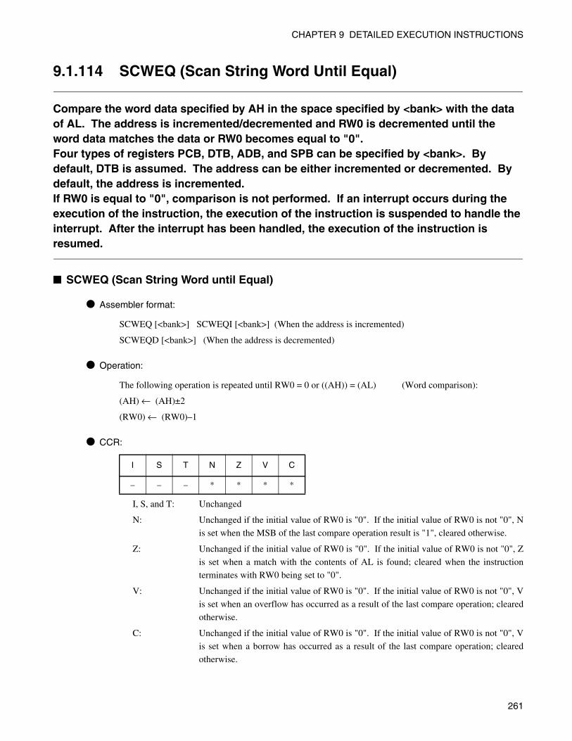
CHAPTER 9 DETAILED EXECUTION INSTRUCTIONS
9.1.114 SCWEQ (Scan String Word Until Equal)
Compare the word data specified by AH in the space specified by <bank> with the data of AL. The address is incremented/decremented and RW0 is decremented until the word data matches the data or RW0 becomes equal to "0". Four types of registers PCB, DTB, ADB, and SPB can be specified by <bank>. By default, DTB is assumed. The address can be either incremented or decremented. By default, the address is incremented. If RW0 is equal to "0", comparison is not performed. If an interrupt occurs during the execution of the instruction, the execution of the instruction is suspended to handle the interrupt. After the interrupt has been handled, the execution of the instruction is resumed.
■ SCWEQ (Scan String Word until Equal)
● Assembler format:
SCWEQ [<bank>] SCWEQI [<bank>] (When the address is incremented)
SCWEQD [<bank>] (When the address is decremented)
● Operation:
The following operation is repeated until RW0 = 0 or ((AH)) = (AL) (Word comparison):
(AH) ← (AH)±2
(RW0) ← (RW0)–1
● CCR:
I, S, and T: Unchanged
N: Unchanged if the initial value of RW0 is "0". If the initial value of RW0 is not "0", N
is set when the MSB of the last compare operation result is "1", cleared otherwise.
Z: Unchanged if the initial value of RW0 is "0". If the initial value of RW0 is not "0", Z
is set when a match with the contents of AL is found; cleared when the instruction
terminates with RW0 being set to "0".
V: Unchanged if the initial value of RW0 is "0". If the initial value of RW0 is not "0", V
is set when an overflow has occurred as a result of the last compare operation; cleared
otherwise.
C: Unchanged if the initial value of RW0 is "0". If the initial value of RW0 is not "0", V
is set when a borrow has occurred as a result of the last compare operation; cleared
otherwise.
I S T N Z V C
– – – * * * *
261
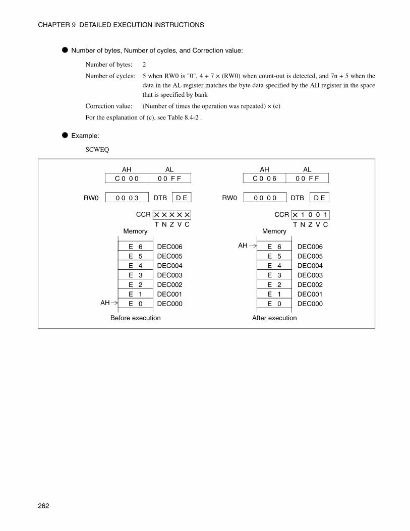
CHAPTER 9 DETAILED EXECUTION INSTRUCTIONS
● Number of bytes, Number of cycles, and Correction value:
Number of bytes: 2
Number of cycles: 5 when RW0 is "0", 4 + 7 × (RW0) when count-out is detected, and 7n + 5 when the
data in the AL register matches the byte data specified by the AH register in the space
that is specified by bank
Correction value: (Number of times the operation was repeated) × (c)
For the explanation of (c), see Table 8.4-2 .
● Example:
SCWEQ
0 0 0 3RW0
Before execution
E 6 DEC006E 5 DEC005E 4 DEC004
D EDTB
AH AL
E 3 DEC003
0 0 0 0RW0 D EDTB
AH AL
E 2 DEC002E 1 DEC001E 0 DEC000AH
Memory
After execution
E 6 DEC006E 5 DEC005E 4 DEC004E 3 DEC003E 2 DEC002E 1 DEC001E 0 DEC000
AH
Memory
C 0 0 0 0 0 F F C 0 0 6 0 0 F F
CCR × × × × ×T N Z V C
CCR × 1 0 0 1
T N Z V C
262

CHAPTER 9 DETAILED EXECUTION INSTRUCTIONS
9.1.115 SETB (Set Bit)
Set the contents of the bit address specified by the operand to "1".
■ SETB (Set Bit)
● Assembler format:
SETB addr16:bp
SETB dir:bp
SETB io:bp
● Operation:
(Operand) b ← 1 (Bit transfer)
● CCR:
None of the flags is changed.
● Number of bytes, Number of cycles, and Correction value:
For the explanation of (b) in the table, see Table 8.4-2 .
● Example:
SETB 0AA55H:4
I S T N Z V C
– – – – – – –
Operand ad16:bp dir:bp io:bp
Number of bytes 4 3 3
Number of cycles 7 7 7
Correction value 2×(b) 2×(b) 2×(b)
Before execution
Memory
× ×6 F AA55× ×
After execution
Memory
× ×7 F AA55× ×
0 0 0 0 0CCRT N Z V C
0 0 0 0 0CCRT N Z V C
263

CHAPTER 9 DETAILED EXECUTION INSTRUCTIONS
9.1.116 SUB (Subtract Byte Data of Source from Destination to Destination)
Subtract the byte data specified by the second operand from the byte data specified by the first operand and restore the result in the first operand. If the first operand is A, "0" is transferred to bits 8 to 15 of A.
■ SUB (Subtract Byte Data of Source from Destination to Destination)
● Assembler format:
SUB A,#imm8 SUB A,dir
SUB A,ear SUB A,eam
SUB ear,A SUB eam,A
● Operation:
(First operand) ← (First operand)–(Second operand) (Byte subtraction)
● CCR:
I, S, and T: Unchanged
N: Set when the MSB of the operation result is "1", cleared otherwise.
Z: Set when the operation result is "0", cleared otherwise.
V: Set when an overflow has occurred as a result of the operation, cleared otherwise.
C: Set when a borrow has occurred as a result of the operation, cleared otherwise.
● Number of bytes, Number of cycles, and Correction value:
For the explanation of (a) and (b) in the table, see Table 8.4-1 and Table 8.4-2 .
I S T N Z V C
– – – * * * *
First operand A A A A ear eam
Second operand #im8 dir ear eam A A
Number of bytes 2 2 2 2+ 2 2+
Number of cycles 2 5 3 4+(a) 3 5+(a)
Correction value 0 (b) 0 (b) 0 2×(b)
264

CHAPTER 9 DETAILED EXECUTION INSTRUCTIONS
● Example:
SUB A,#22H
Before execution After execution
CCR × × × × ×T N Z V C
CCR × 1 0 0 1
T N Z V C
× × × × 4 9 0 1 A × × × × 0 0 D F A
265

CHAPTER 9 DETAILED EXECUTION INSTRUCTIONS
9.1.117 SUBC (Subtract Byte Data of AL from AH with Carry to AL)
Subtract the low-order byte data of AL and the carry bit (C) from the low-order byte data of AH and restore the result in AL. "0" is transferred to bits 8 to 15 of the accumulator (A).
■ SUBC (Subtract Byte Data of AL from AH with Carry to AL)
● Assembler format:
SUBC A
● Operation:
(AL) ← (AH)–(AL)–(C) (Byte subtraction with a carry)
● CCR:
I, S, and T: Unchanged
N: Set when the MSB of the operation result is "1", cleared otherwise.
Z: Set when the operation result is "0", cleared otherwise.
V: Set when an overflow has occurred as a result of the operation, cleared otherwise.
C: Set when a borrow has occurred as a result of the operation, cleared otherwise.
● Number of bytes, Number of cycles, and Correction value:
Number of bytes: 1
Number of cycles: 2
Correction value: 0
● Example:
SUBC A
I S T N Z V C
– – – * * * *
0 5 0 5 0 0 D 4 A
Before execution
0 5 0 5 0 0 3 0 A
After execution
CCR × × × × ×T N Z V C
CCR × 1 0 0 1
T N Z V C
266

CHAPTER 9 DETAILED EXECUTION INSTRUCTIONS
9.1.118 SUBC (Subtract Byte Data of Effective Address from Accumulator with Carry to Accumulator)
Subtract the byte data specified by the second operand and the carry bit (C) from the byte data of the accumulator (A) and restore the result in A. "0" is transferred to bits 8 to 15 of A.
■ SUBC (Subtract Byte Data of Effective Address from Accumulator with Carry to Accumulator)
● Assembler format:
SUBC A,ear SUBC A,eam
● Operation:
(A) ← (A)–(Second operand)–(C) (Byte subtraction with a carry)
● CCR:
I, S, and T: Unchanged
N: Set when the MSB of the operation result is "1", cleared otherwise.
Z: Set when the operation result is "0", cleared otherwise.
V: Set when an overflow has occurred as a result of the operation, cleared otherwise.
C: Set when a borrow has occurred as a result of the operation, cleared otherwise.
● Number of bytes, Number of cycles, and Correction value:
For the explanation of (a) and (b) in the table, see Table 8.4-1 and Table 8.4-2 .
I S T N Z V C
– – – * * * *
First operand A A
Second operand ear eam
Number of bytes 2 2+
Number of cycles 3 4+(a)
Correction value 0 (b)
267

CHAPTER 9 DETAILED EXECUTION INSTRUCTIONS
● Example:
SUBC A,R1
Before execution After execution
5 4R1 5 4R1
× × × × 0 0 3 5 A × × × × 0 0 E 1 A
CCR × × × × 0
T N Z V C
CCR × 1 0 0 1
T N Z V C
268

CHAPTER 9 DETAILED EXECUTION INSTRUCTIONS
9.1.119 SUBCW (Subtract Word Data of Effective Address from Accumulator with Carry to Accumulator)
Subtract the word data specified by the second operand and the carry bit (C) from the low-order word data of the accumulator (A) and restore the result in A.
■ SUBCW (Subtract Word Data of Effective Address from Accumulator with Carry to Accumulator)
● Assembler format:
SUBCW A,ear SUBCW A,eam
● Operation:
(A) ← (A)–(Second operand)–(C) (Word subtraction with a carry)
● CCR:
I, S, and T: Unchanged
N: Set when the MSB of the operation result is "1", cleared otherwise.
Z: Set when the operation result is "0", cleared otherwise.
V: Set when an overflow has occurred as a result of the operation, cleared otherwise.
C: Set when a borrow has occurred as a result of the operation, cleared otherwise.
● Number of bytes, Number of cycles, and Correction value:
For the explanation of (a) and (b) in the table, see Table 8.4-1 and Table 8.4-2 .
I S T N Z V C
– – – * * * *
First operand A A
Second operand ear eam
Number of bytes 2 2+
Number of cycles 3 4+(a)
Correction value 0 (b)
269

CHAPTER 9 DETAILED EXECUTION INSTRUCTIONS
● Example:
SUBCW A,0E024H
Before execution After execution
Memory Memory
A 9 E025 A 9 E0255 B E024 5 B E024
× × × × 7 5 5 8A × × × × C B F C A
CCR × × × × 1
T N Z V C
CCR × 1 0 0 1
T N Z V C
270

CHAPTER 9 DETAILED EXECUTION INSTRUCTIONS
9.1.120 SUBDC (Subtract Decimal Data of AL from AH with Carry to AL)
Subtract the low-order byte data of AL and the carry bit (C) from the low-order byte data of AH and restore the result in AL. "0" is transferred to bits 8 to 15 of A.
■ SUBDC (Subtract Decimal Data of AL from AH with Carry to AL)
● Assembler format:
SUBDC A
● Operation:
(AL) ← (AH)–(AL)–(C) (Decimal subtraction with a carry)
● CCR:
I, S, and T: Unchanged
N: Set when the MSB of the operation result is "1", cleared otherwise.
Z: Set when the operation result is "0", cleared otherwise.
V: Undefined
C: Set when a borrow has occurred as a result of the decimal operation, cleared otherwise.
● Number of bytes, Number of cycles, and Correction value:
Number of bytes: 1
Number of cycles: 3
Correction value: 0
● Example:
SUBDC A
I S T N Z V C
– – – * * * *
× × 8 6 × × 8 6 A
Before execution
× × 8 6 0 0 0 0 A
After execution
CCR × × × × 0
T N Z V C
CCR × 0 1 0 0
T N Z V C
271

CHAPTER 9 DETAILED EXECUTION INSTRUCTIONS
9.1.121 SUBL (Subtract Long Word Data of Source from Destination to Destination)
Subtract the long word data specified by the second operand from the long word data of the accumulator (A) and restore the result in A.
■ SUBL (Subtract Long Word Data of Source from Destination to Destination)
● Assembler format:
SUBL A,#imm32
SUBL A,ear SUBL A,eam
● Operation:
(First operand) ← (First operand)–(Second operand) (Long word subtraction)
● CCR:
I, S, and T: Unchanged
N: Set when the MSB of the operation result is "1", cleared otherwise.
Z: Set when the operation result is "0", cleared otherwise.
V: Set when an overflow has occurred as a result of the operation, cleared otherwise.
C: Set when a borrow has occurred as a result of the operation, cleared otherwise.
● Number of bytes, Number of cycles, and Correction value:
For the explanation of (a) and (d) in the table, see Table 8.4-1 and Table 8.4-2 .
I S T N Z V C
– – – * * * *
First operand A A A
Second operand #i32 ear eam
Number of bytes 5 2 2+
Number of cycles 4 6 7+(a)
Correction value 0 0 (d)
272

CHAPTER 9 DETAILED EXECUTION INSTRUCTIONS
● Example:
SUBL A,0FD12H
3 4 B 3 F 2 0 1 A
Before execution
E 2 5 4 C 0 4 4 A
After execution
Memory Memory
FD16 FD165 2 FD15 5 2 FD155 F FD14 5 F FD143 1 FD13 3 1 FD13B D FD12 B D FD12
CCR × × × × ×T N Z V C
CCR × 1 0 0 1
T N Z V C
273

CHAPTER 9 DETAILED EXECUTION INSTRUCTIONS
9.1.122 SUBW (Subtract Word Data of Source from Destination to Destination)
Subtract the word data specified by the second operand from the word data specified by the first operand and restore the result in the first operand.
■ SUBW (Subtract Word Data of Source from Destination to Destination)
● Assembler format:
SUBW A,#imm16
SUBW A,ear SUBW A,eam
SUBW ear,A SUBW eam,A
● Operation:
(First operand) ← (First operand)–(Second operand) (Word subtraction)
● CCR:
I, S, and T: Unchanged
N: Set when the MSB of the operation result is "1", cleared otherwise.
Z: Set when the operation result is "0", cleared otherwise.
V: Set when an overflow has occurred as a result of the operation, cleared otherwise.
C: Set when a borrow has occurred as a result of the operation, cleared otherwise.
● Number of bytes, Number of cycles, and Correction value:
For the explanation of (a) and (c) in the table, see Table 8.4-1 and Table 8.4-2 .
I S T N Z V C
– – – * * * *
First operand A A A ear eam
Second operand #i16 ear eam A A
Number of bytes 3 2 2+ 2 2+
Number of cycles 2 3 4+(a) 3 5+(a)
Correction value 0 0 (c) 0 2×(c)
274

CHAPTER 9 DETAILED EXECUTION INSTRUCTIONS
● Example:
SUBW @RW0+,A
× × × × 3 1 0 4 A
E 2 A 4 RW0
× × × × 3 1 0 4 A
E 2 A 6 RW0
Before execution After execution
Memory Memory
5 D E2A5 2 C E2A5A B E2A4 A 7 E2A4
CCR × × × × ×T N Z V C
CCR × 0 0 0 0
T N Z V C
275

CHAPTER 9 DETAILED EXECUTION INSTRUCTIONS
9.1.123 SUBW (Subtract Word Data of AL from AH to AL)
Subtract the word data of AL from the word data of AH and restore the result to AL.
■ SUBW (Subtract Word Data of AL from AH to AL)
● Assembler format:
SUBW A
● Operation:
(AL) ← (AH)–(AL) (Word subtraction)
● CCR:
I, S, and T: Unchanged
N: Set when the MSB of the operation result is "1", cleared otherwise.
Z: Set when the operation result is "0", cleared otherwise.
V: Set when an overflow has occurred as a result of the operation, cleared otherwise.
C: Set when a borrow has occurred as a result of the operation, cleared otherwise.
● Number of bytes, Number of cycles, and Correction value:
Number of bytes: 1
Number of cycles: 2
Correction value: 0
● Example:
SUBW A
I S T N Z V C
– – – * * * *
8 3 A 2 1 0 1 9 A
Before execution
8 3 A 2 7 3 8 9 A
After execution
CCR × × × × ×T N Z V C
CCR × 0 0 1 0
T N Z V C
276

CHAPTER 9 DETAILED EXECUTION INSTRUCTIONS
9.1.124 SWAP (Swap Byte Data of Accumulator)
Swap the high- and low-order bytes of the word data for the accumulator (A) with each other.
■ SWAP (Swap Byte Data of Accumulator)
● Assembler format:
SWAP
● Operation:
(A) 0 to 7 ↔ (A) 8 to 15 (Byte swapping)
● CCR:
None of the flags is changed.
● Number of bytes, Number of cycles, and Correction value:
Number of bytes: 1
Number of cycles: 3
Correction value: 0
● Example:
SWAP
I S T N Z V C
– – – – – – –
× × × × 0 6 9 0 A
Before execution
× × × × 9 0 0 6 A
After execution
CCR × × × × ×T N Z V C
CCR × × × × ×T N Z V C
277
CHAPTER 9 DETAILED EXECUTION INSTRUCTIONS
9.1.125 SWAPW (Swap Word Data of Accumulator)
Swap the high- and low-order words of the long word data for the accumulator (A) with each other.
■ SWAPW (Swap Word Data of Accumulator)
● Assembler format:
SWAPW
● Operation:
Bits 0 to 15 of A ↔ Bits 16 to 31 of A (Word swapping)
● CCR:
None of the flags is changed.
● Number of bytes, Number of cycles, and Correction value:
Number of bytes: 1
Number of cycles: 2
Correction value: 0
● Example:
SWAPW
I S T N Z V C
– – – – – – –
1 9 8 6 9 8 6 1 A
Before execution
9 8 6 1 1 9 8 6 A
After execution
CCR × × × × ×T N Z V C
CCR × × × × ×T N Z V C
278

CHAPTER 9 DETAILED EXECUTION INSTRUCTIONS
9.1.126 UNLINK (Unlink and Create New Stack Frame)
Restore an old frame pointer from a stack.
■ UNLINK (Unlink and Create New Stack Frame)
● Assembler format:
UNLINK
● Operation:
(sp) ← (RW3), (RW3) ← ((sp)), (sp) ← (sp)+2
● CCR:
None of the flags is changed.
● Number of bytes, Number of cycles, and Correction value:
Number of bytes: 1
Number of cycles: 5
Correction value: (c)
For the explanation of (c), see Table 8.4-2 .
● Example:
UNLINK
I S T N Z V C
– – – – – – –
Before execution
Memory
A 04 6 E020
E 0 0 0SP
SP × × E000
E 0 2 0RW3
E 0 2 2SP
A 0 4 6RW3
After execution
Memory
× × E022
4 6 E020
SPA 0 E021
279

CHAPTER 9 DETAILED EXECUTION INSTRUCTIONS
9.1.127 WBTc (Wait until Bit Condition Satisfied)
This instruction keeps reading data from the bit address specified by the operand until that data satisfies the conditions. Once the data at the specified bit address satisfies the conditions, control is transferred to the instruction subsequent to the WBTc instruction.
■ WBTc (Wait until Bit Condition Satisfied)
● Assembler format:
WBTC io:bp
WBTS io:bp
● Operation:
Data is read from the bit address specified by io:bp until the data satisfies the condition. If the data from
the bit address satisfies the condition, control is transferred to the next instruction.
Interrupts are acceptable while the read operation is repeated with the condition not satisfied. If an
interrupt is generated in this state, the RETI instruction causes control to return to the WBTc instruction,
not to the instruction following the WBTc instruction.
● CCR:
None of the flags is changed.
● Number of bytes, Number of cycles, and Correction value:
I S T N Z V C
– – – – – – –
Instruction WBTC WBTS
Condition Bit data=0 Bit data=1
Number of bytes 3 3
Number of cycles Undefined Undefined
Correction value Until the condition is satisfied Until the condition is satisfied
280

CHAPTER 9 DETAILED EXECUTION INSTRUCTIONS
● Example:
WBTS 34H:7
Before execution
Memory
× ×7 F 0034H
× ×
E 1 0 0PC
After execution
Peripheralregister
Data is read from address 34H until bit 7 is set to "1" (because of resource operation, for example). When bit 7 becomes "1", execute the next instruction.
281

CHAPTER 9 DETAILED EXECUTION INSTRUCTIONS
9.1.128 XCH (Exchange Byte Data of Source to Destination)
Exchange the byte data specified by the first operand with that specified by the second operand. If the first operand is A, the high-order byte of AL is set to 00H.
■ XCH (Exchange Byte Data of Source to Destination)
● Assembler format:
XCH A,ear XCH A,eam
XCH Ri,ear XCH Ri,eam
● Operation:
(First operand) ↔ (Second operand) (Byte exchange)
● CCR:
None of the flags is changed.
● Number of bytes, Number of cycles, and Correction value:
For the explanation of (a) and (b) in the table, see Table 8.4-1 and Table 8.4-2 .
I S T N Z V C
– – – – – – –
First operand A A Ri Ri
Second operand ear eam ear eam
Number of bytes 2 2+ 2 2+
Number of cycles 4 5+(a) 7 9+(a)
Correction value 0 2×(b) 0 2×(b)
282

CHAPTER 9 DETAILED EXECUTION INSTRUCTIONS
● Example:
XCH R4,@RW0+
0 0 6 0RW0
F 1R4
Before execution After execution
Memory
0061
Memory
0061
2 2 0060 F 1 0060
0 0 6 1 RW0
2 2R4
RW0RW0
CCR × × × × ×T N Z V C
CCR × × × × ×T N Z V C
283

CHAPTER 9 DETAILED EXECUTION INSTRUCTIONS
9.1.129 XCHW (Exchange Word Data of Source to Destination)
Exchange the word data specified by the first operand with that specified by the second operand.
■ XCHW (Exchange Word Data of Source to Destination)
● Assembler format:
XCHW A,ear XCHW A,eam
XCHW RWi,ear XCHW RWi,eam
● Operation:
(First operand) ↔ (Second operand) (Word exchange)
● CCR:
None of the flags is changed.
● Number of bytes, Number of cycles, and Correction value:
For the explanation of (a) and (c) in the table, see Table 8.4-1 and Table 8.4-2 .
I S T N Z V C
– – – – – – –
First operand A A RWi RWi
Second operand ear eam ear eam
Number of bytes 2 2+ 2 2+
Number of cycles 4 5+(a) 7 9+(a)
Correction value 0 2×(c) 0 2×(c)
284

CHAPTER 9 DETAILED EXECUTION INSTRUCTIONS
● Example:
XCHW A,@RW0
× × × × 3 4 B 4 A
RW0
× × × × 2 D 5 8 A
RW0
Before execution After execution
Memory Memory
2 D E002 3 4 E0025 8 E001 B 4 E001RW0 RW0
E 0 0 1 E 0 0 1
CCR × × × × ×T N Z V C
CCR × × × × ×T N Z V C
285

CHAPTER 9 DETAILED EXECUTION INSTRUCTIONS
9.1.130 XOR (Exclusive Or Byte Data of Destination and Source to Destination)
Take the logical exclusive OR of the byte data specified by the first operand and the byte data specified by the second operand and restore the result in the first operand.
■ XOR (Exclusive Or Byte Data of Destination and Source to Destination)
● Assembler format:
XOR A,#imm8
XOR A,ear XOR A,eam
XOR ear,A XOR eam,A
● Operation:
(First operand) ← (First operand) xor (Second operand) (Byte logical exclusive OR)
● CCR:
I, S, and T: Unchanged
N: Set when the MSB of the operation result is "1", cleared otherwise.
Z: Set when the operation result is "0", cleared otherwise.
V: Cleared
C: Unchanged
● Number of bytes, Number of cycles, and Correction value:
For the explanation of (a) and (b) in the table, see Table 8.4-1 and Table 8.4-2 .
I S T N Z V C
– – – * * R –
First operand A A A ear eam
Second operand #im8 ear eam A A
Number of bytes 2 2 2+ 2 2+
Number of cycles 2 3 4+(a) 3 5+(a)
Correction value 0 0 (b) 0 2×(b)
286

CHAPTER 9 DETAILED EXECUTION INSTRUCTIONS
● Example:
XOR 0052H,A
× × × × 0 0 5 5A
Before execution
× × × × 0 0 5 5A
After execution
Memory Memory
F A 000052 A F 000052
CCR × × × × ×T N Z V C
CCR × 1 0 0 ×T N Z V C
287

CHAPTER 9 DETAILED EXECUTION INSTRUCTIONS
9.1.131 XORL (Exclusive Or Long Word Data of Destination and Source to Destination)
Take the logical exclusive OR of the long word data for the accumulator (A) and that specified by the second operand and restore the result in A.
■ XORL (Exclusive Or Long Word Data of Destination and Source to Destination)
● Assembler format:
XORL A,ear XORL A,eam
● Operation:
(A) ← (A) xor (Second operand) (Long word logical exclusive OR)
● CCR:
I, S, and T: Unchanged
N: Set when the MSB of the operation result is "1", cleared otherwise.
Z: Set when the operation result is "0", cleared otherwise.
V: Cleared
C: Unchanged
● Number of bytes, Number of cycles, and Correction value:
For the explanation of (a) and (d) in the table, see Table 8.4-1 and Table 8.4-2 .
I S T N Z V C
– – – * * R –
First operand A A
Second operand ear eam
Number of bytes 2 2+
Number of cycles 6 7+(a)
Correction value 0 (d)
288
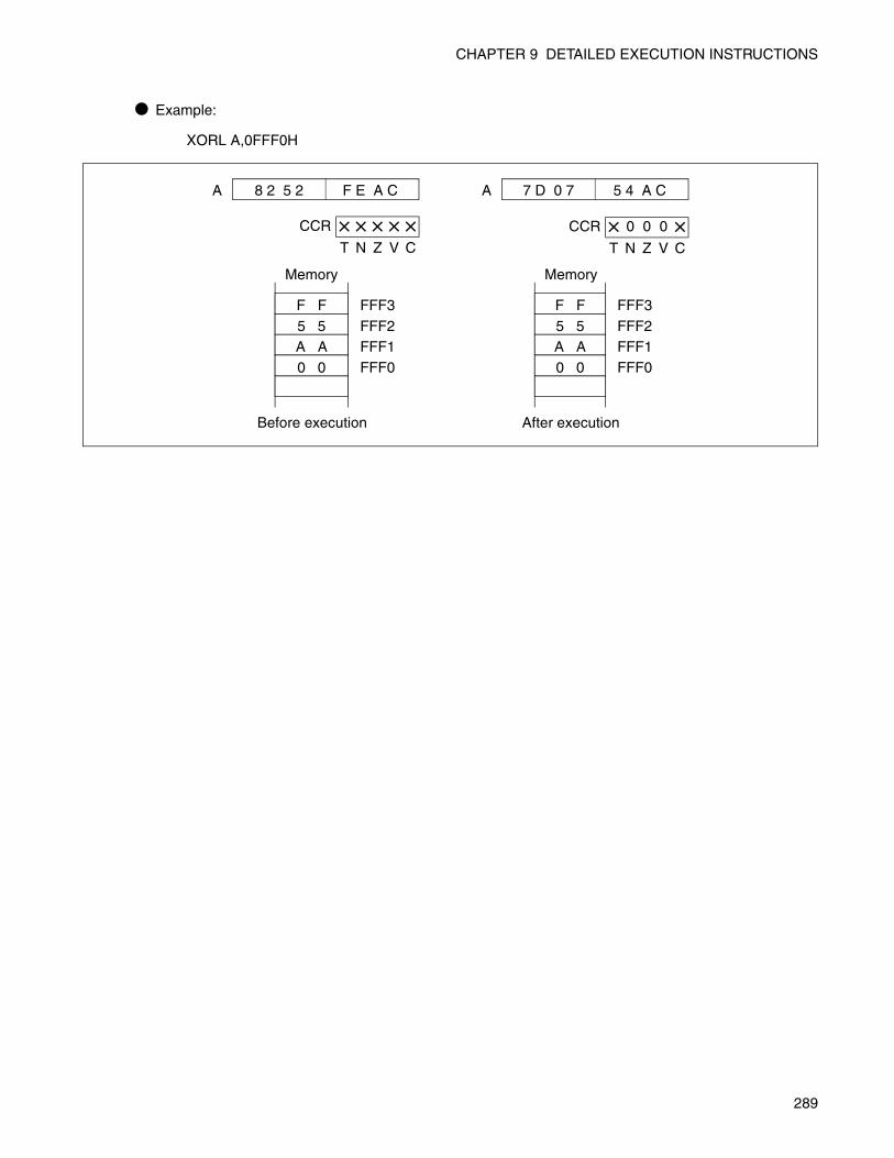
CHAPTER 9 DETAILED EXECUTION INSTRUCTIONS
● Example:
XORL A,0FFF0H
8 2 5 2 F E A C A
Before execution
7 D 0 7 5 4 A C A
After execution
Memory Memory
F F FFF35 5 FFF2A A FFF10 0 FFF0
F F FFF35 5 FFF2A A FFF10 0 FFF0
CCR × × × × ×T N Z V C
CCR × 0 0 0 ×T N Z V C
289

CHAPTER 9 DETAILED EXECUTION INSTRUCTIONS
9.1.132 XORW (Exclusive Or Word Data of AH and AL to AL)
Take the logical exclusive OR for the word data of AH and that of AL and restore the result in AL.
■ XORW (Exclusive Or Word Data of AH and AL to AL)
● Assembler format:
XORW A
● Operation:
(AL) ← (AH) xor (AL) (Word logical exclusive OR)
● CCR:
I, S, and T: Unchanged
N: Set when the MSB of the operation result is "1", cleared otherwise.
Z: Set when the operation result is "0", cleared otherwise.
V: Cleared
C: Unchanged
● Number of bytes, Number of cycles, and Correction value:
Number of bytes: 1
Number of cycles: 2
Correction value: 0
● Example:
XORW A
I S T N Z V C
– – – * * R –
0 4 2 6 A B 9 8 A
Before execution
0 4 2 6 A F B E A
After execution
CCR × × × × ×T N Z V C
CCR × 1 0 0 ×T N Z V C
290

CHAPTER 9 DETAILED EXECUTION INSTRUCTIONS
9.1.133 XORW (Exclusive Or Word Data of Destination and Source to Destination)
Take the logical exclusive OR of the word data specified by the first operand and the word data specified by the second operand and restore the result in the first operand.
■ XORW (Exclusive Or Word Data of Destination and Source to Destination)
● Assembler format:
XORW A,#imm16
XORW A,ear XORW A,eam
XORW ear,A XORW eam,A
● Operation:
(First operand) ← (First operand) xor (Second operand) (Word logical exclusive OR)
● CCR:
I, S, and T: Unchanged
N: Set when the MSB of the operation result is "1", cleared otherwise.
Z: Set when the operation result is "0", cleared otherwise.
V: Cleared
C: Unchanged
● Number of bytes, Number of cycles, and Correction value:
For the explanation of (a) and (c) in the table, see Table 8.4-1 and Table 8.4-2 .
I S T N Z V C
– – – * * R –
First operand A A A ear eam
Second operand #i16 ear eam A A
Number of bytes 3 2 2+ 2 2+
Number of cycles 2 3 4+(a) 3 5+(a)
Correction value 0 0 (c) 0 2×(c)
291

CHAPTER 9 DETAILED EXECUTION INSTRUCTIONS
● Example:
XORW 0E001H,A
Before execution After execution
Memory Memory
8 3 E0024 2 E001
D A E0022 1 E001
× × × × 5 9 6 3 A × × × × 5 9 6 3 A
CCR × × × × ×T N Z V C
CCR × 1 0 0 ×T N Z V C
292

CHAPTER 9 DETAILED EXECUTION INSTRUCTIONS
9.1.134 ZEXT (Zero Extend from Byte Data to Word Data)
Transfer "0" to bits 8 to 15 of the accumulator (A).
■ ZEXT (Zero Extend from Byte Data to Word Data)
● Assembler format:
ZEXT
● Operation:
Bits 8 to 15 of A ← 00H
● CCR:
I, S, and T: Unchanged
N: Cleared
Z: Set when the zero-extended data is "0", cleared otherwise.
V and C: Unchanged
● Number of bytes, Number of cycles, and Correction value:
Number of bytes: 1
Number of cycles: 1
Correction value: 0
● Example:
ZEXT
I S T N Z V C
– – – R * – –
× × × × × × A
Before execution
× × × × 0 0 8 0 A
After execution
8 0
CCR × × × × ×T N Z V C
CCR × 0 0 × ×T N Z V C
293

CHAPTER 9 DETAILED EXECUTION INSTRUCTIONS
9.1.135 ZEXTW (Zero Extend from Word Data to Long Word Data)
Transfer "0" to bits 16 to 31 of the accumulator (A).
■ ZEXTW (Zero Extend from Word Data to Long Word Data)
● Assembler format:
ZEXTW
● Operation:
Bits 16 to 31 of A ← 0000H
● CCR:
I, S, andT: Unchanged
N: Cleared
Z: Set when the zero-extended data is "0", cleared otherwise.
V and C: Unchanged
● Number of bytes, Number of cycles, and Correction value:
Number of bytes: 1
Number of cycles: 1
Correction value: 0
● Example:
ZEXTW
I S T N Z V C
– – – R * – –
× × × × F F 8 0 A
Before execution
0 0 0 0 F F 8 0A
After execution
CCR × × × × ×T N Z V C
CCR × 0 0 × ×T N Z V C
294

APPENDIX
This appendix includes lists and maps of instructions
for the F2MC-16LX.
APPENDIX A Explanation of Instruction Lists
APPENDIX B F2MC-16LX Instruction Lists (351 Instructions)
APPENDIX C F2MC-16LX Instruction Maps
295

APPENDIX
APPENDIX A Explanation of Instruction Lists
This section explains items and symbols used in each instruction list included in Appendix B.
A.1 Items Used in Instruction Lists
A.2 Symbols Used in Instruction Lists
A.3 Effective Address Field
A.4 Calculating the Number of Execution Cycles
296

APPENDIX A Explanation of Instruction Lists
A.1 Items Used in Instruction Lists
Table A-1 explains the items used in the instruction lists.
■ Explanation of the Items Used in the Instruction Lists
Table A-1 Explanation of the Items Used in the Instruction Lists (1 / 2)
Item Description
MnemonicUpper-case letters and symbols: Described as they appear in assembler.Lower-case letters: Replaced when described in assembler.Numbers after lower-case letters: Indicate the bit width within the instruction.
# Indicates the number of bytes.
~Indicates the number of cycles.See Table A-4 for details about meanings of letters in items.
RGIndicates the register access count during execution of instruction.Used to calculate compensation values for CPU intermittent operation.
B
Indicates the compensation value for calculating the number of actual cycles during execution of instruction.The number of actual cycles during execution of instruction is the compensation value summed with the value in the "~" column.
Operation Indicates operation of instruction.
LH
Indicates special operations involving bits 15 through 08 of the accumulator.Z: Transfers "0".X: Sign-extended transfer through sign extension.- : Transfers nothing.
AH
Indicates special operations involving the high-order 16 bits in the accumulator.*: Transfers from AL to AH.- : No transferZ: Transfers 00H to AH.X: Transfers 00H or FFH to AH using sign extension AL.
I Indicates the status of each of the following flags: I (interrupt enable), S (stack), T (sticky bit), N (negative), Z (zero), V (overflow), and C (carry).
*: Changes due to execution of instruction.- : No changeS: Set by execution of instruction.R: Reset by execution of instruction.
S
T
N
Z
V
C
297

APPENDIX
■ Number of Execution CyclesThe number of cycles required to execute instructions (number of execution cycles) is the summation of the
number of cycles of each instruction, the compensation value determined by conditions, and the number of
cycles required to fetch programs. If, however, a program stored in memory that is connected to a 16-bit
bus such as internal ROMs is to be fetched, program fetch is executed every time instructions being
executed exceed the two byte (one word) boundary. Therefore, interference with data access will increase
the number of execution cycles. Since program fetch is executed for each byte of instructions being
executed when a program stored on the memory connected to an external 8-bit bus is fetched, data access
interference will increase the number of execution cycles.
When access is made to general-purpose registers, built-in ROMs, built-in RAMs, built-in I/O units, or
external buses during CPU intermittent operation, the CPU clock suspends its operation for the number of
cycles that is specified by the CG0/CG1 bit of the low-power-consumption-mode control register. Therefore,
to obtain the number of cycles required to execute instructions during CPU intermittent operation, add
these compensation values (the number of accesses multiplied by the number of cycled suspended) to the
number of normal execution cycles.
RMW
Indicates whether the instruction is a read-modify-write instruction (a single instruction that reads data from memory, etc., processes the data, and then writes the result to memory.).
*: Instruction is a read-modify-write instruction.-: Instruction is not a read-modify-write instruction.
Note:A read-modify-write instruction cannot be used on addresses that have different meanings depending on whether they are read or written.
Table A-1 Explanation of the Items Used in the Instruction Lists (2 / 2)
Item Description
298

APPENDIX A Explanation of Instruction Lists
A.2 Symbols Used in Instruction Lists
Table A-2 explains the symbols used in the instruction lists.
■ Explanation of the Symbols Used in the Instruction Lists
Table A-2 Explanation of the Symbols Used in the Instruction Lists (1 / 2)
Symbol Explanation
A
32 bit accumulator The bit length used is different for each instruction.
Byte: Lower 8 bits of ALWord: 16 bits of ALLong: 32 bits of AL and AH
AH Upper 16 bits of A
AL Lower 16 bits of A
SP Stack pointer (USP or SSP)
PC Program counter
PCB Program bank register
DTB Data bank register
ADB Additional data bank register
SSB System stack bank register
USB User stack bank register
DPR Direct page register
brg1 DTB, ADB, SSB, USB, DPR, PCB
brg2 DTB, ADB, SSB, USB, DPR
Ri R0, R1, R2, R3, R4, R5, R6, R7
Rj R0, R1, R2, R3
RWi RW0, RW1, RW2, RW3, RW4, RW5, RW6, RW7
RWj RW0, RW1, RW2, RW3
RLi RL0, RL1, RL2, RL3
dir Abbreviated direct addressing
addr16 Direct addressing
addr24 Physical direct addressing
ad24 0-15 Bit0 to bit15 of address 24
ad24 16-23 Bit16 to bit23 of address 24
299

APPENDIX
io I/O area (000000H to 0000FFH)
imm4 4-bit immediate data
imm8 8-bit immediate data
imm16 16-bit immediate data
imm32 32-bit immediate data
ext (imm8) 16-bit data signed and extended from 8-bit immediate data
disp8 8-bit displacement
disp16 16-bit displacement
bp Bit offset value
vct4 Vector number (0 to 15)
vct8 Vector number (0 to 255)
( ) b Bit address
rel Branch specification relative to PC
ear Effective addressing (codes 00 to 07)
eam Effective addressing (codes 08 to 1F)
rlst Register list
Table A-2 Explanation of the Symbols Used in the Instruction Lists (2 / 2)
Symbol Explanation
300

APPENDIX A Explanation of Instruction Lists
A.3 Effective Address Field
Table A-3 lists address formats used in the effective address field.
■ Effective Address Field
Table A-3 Effective Address Field
Code Notation Address formatNumber of bytes
of address expansion part*
00 R0 RW0 RL0
Register direct Starting from the left, "ea" corresponds to the byte, word and long-word types.
-
01 R1 RW1 (RL0)
02 R2 RW2 RL1
03 R3 RW3 (RL1)
04 R4 RW4 RL2
05 R5 RW5 (RL2)
06 R6 RW6 RL3
07 R7 RW7 (RL3)
08 @RW0
Register indirect 009 @RW1
0A @RW2
0B @RW3
0C @RW0+
Register indirect with post-incrementing 00D @RW1+
0E @RW2+
0F @RW3+
10 @RW0+disp8
Register indirect with 8-bit displacement 1
11 @RW1+disp8
12 @RW2+disp8
13 @RW3+disp8
14 @RW4+disp8
15 @RW5+disp8
16 @RW6+disp8
17 @RW7+disp8
18 @RW0+disp16
Register indirect with 16-bit displacement 219 @RW1+disp16
1A @RW2+disp16
1B @RW3+disp16
1C @RW0+RW7 Register indirect with index 0
1D @RW1+RW7 Register indirect with index 0
1E @PC+disp16 PC indirect with 16-bit displacement 2
1F addr16 Direct address 2
* : The number of bytes of the address expansion part is shown in the "#" (number of bytes) column or the figure before "+" in the expression of bytes in the instruction details.
301
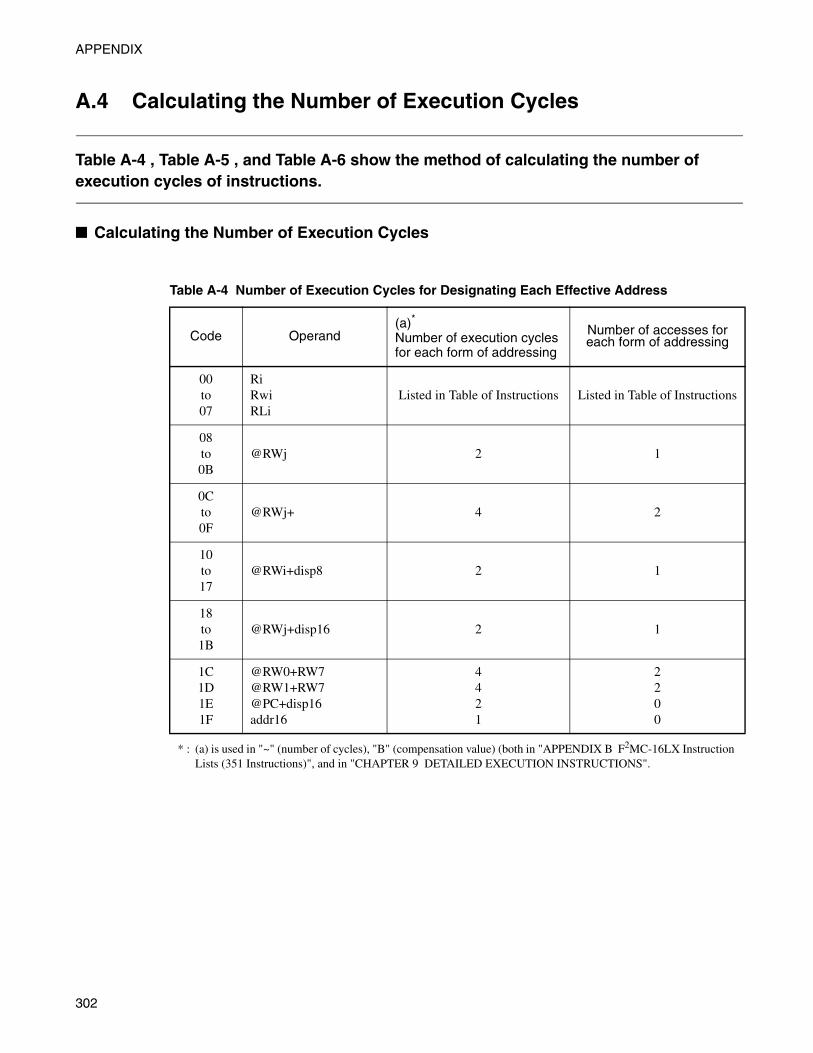
APPENDIX
A.4 Calculating the Number of Execution Cycles
Table A-4 , Table A-5 , and Table A-6 show the method of calculating the number of execution cycles of instructions.
■ Calculating the Number of Execution Cycles
Table A-4 Number of Execution Cycles for Designating Each Effective Address
Code Operand(a)*
Number of execution cycles for each form of addressing
Number of accesses for each form of addressing
00to07
RiRwiRLi
Listed in Table of Instructions Listed in Table of Instructions
08to0B
@RWj 2 1
0Cto0F
@RWj+ 4 2
10to17
@RWi+disp8 2 1
18to1B
@RWj+disp16 2 1
1C1D1E1F
@RW0+RW7@RW1+RW7@PC+disp16addr16
4421
2200
* : (a) is used in "~" (number of cycles), "B" (compensation value) (both in "APPENDIX B F2MC-16LX Instruction Lists (351 Instructions)", and in "CHAPTER 9 DETAILED EXECUTION INSTRUCTIONS".
302

APPENDIX A Explanation of Instruction Lists
Note:
If external data buses are used, add the number of cycles that are weighted with ready input andautomatic ready.
Notes:
• If external data buses are used, add the number of cycles that are weighted with ready input andautomatic ready.
• Since all cases of program fetch do not delay the execution of instructions, use this compensationvalue to calculate the worst case value.
Table A-5 Compensation Values for Calculating the Number of Execution Cycles
Operand(b) byte * (c) word * (d) long *
Cycles Access count Cycles Access
count Cycles Access count
Internal register +0 1 +0 1 +0 2
Internal register even address
+0 1 +0 1 +0 2
Internal register odd address
+0 1 +2 2 +4 4
Even address on external data bus (16-bits)
+1 1 +1 1 +2 2
Odd address on external data bus (16-bits)
+1 1 +4 2 +8 4
External data bus(8-bit)
+1 1 +4 2 +8 4
* : (b), (c), and (d) are used in "~" (number of cycles), "B" (compensation value) (both in "APPENDIX B F2MC-16LX Instruction Lists (351 Instructions)", and in "CHAPTER 9 DETAILED EXECUTION INSTRUCTIONS".
Table A-6 Compensation Values for Calculating The Number of Program Fetch Cycles
Instruction Byte boundary Word boundary
Internal memory - +2
External data bus (16-bit) - +3
External data bus (8-bit) +3 -
303

APPENDIX
APPENDIX B F2MC-16LX Instruction Lists (351 Instructions)
This appendix lists the instructions used in assembler.For items and symbols for each instruction list, see "APPENDIX A Explanation of Instruction Lists".
B.1 Transfer Instructions
B.2 Numeric Data Operation Instructions
B.3 Logical Data Operation Instruction
B.4 Shift Instruction
B.5 Branch Instructions
B.6 Other Instructions
304

APPENDIX B F2MC-16LX Instruction Lists (351 Instructions)
B.1 Transfer Instructions
Table B-1 and Table B-2 lists the transfer instructions of the F2MC-16LX.• Transfer instruction (Byte): 41 instructions in Table B-1 • Transfer instruction (Word/Long-word): 38 instructions in Table B-2
■ Transfer Instructions
Table B-1 Transfer Instruction (Byte): 41 Instructions
Mnemonic # ~ RG B Operation LH AH I S T N Z V C RMW
MOV A,dir 2 3 0 (b) byte (A) ← (dir) Z * - - - * * - - -MOV A,addr16 3 4 0 (b) byte (A) ← (addr16) Z * - - - * * - - -MOV A,Ri 1 2 1 0 byte (A) ← (Ri) Z * - - - * * - - -MOV A,ear 2 2 1 0 byte (A) ← (ear) Z * - - - * * - - -MOV A,eam 2+ 3 + (a) 0 (b) byte (A) ← (eam) Z * - - - * * - - -MOV A,io 2 3 0 (b) byte (A) ← (io) Z * - - - * * - - -MOV A,#imm8 2 2 0 0 byte (A) ← (imm8) Z * - - - * * - - -MOV A,@A 2 3 0 (b) byte (A) ← ((A)) Z - - - - * * - - -MOV A,@RLi+disp8 3 10 2 (b) byte (A) ← ((RLi)+disp8) Z * - - - * * - - -MOVN A,#imm4 1 1 0 0 byte (A) ← imm4 Z * - - - R * - - -MOVX A,dir 2 3 0 (b) byte (A) ← (dir) X * - - - * * - - -MOVX A,addr16 3 4 0 (b) byte (A) ← (addr16) X * - - - * * - - -MOVX A,Ri 2 2 1 0 byte (A) ← (Ri) X * - - - * * - - -MOVX A,ear 2 2 1 0 byte (A) ← (ear) X * - - - * * - - -MOVX A,eam 2+ 3 + (a) 0 (b) byte (A) ← (eam) X * - - - * * - - -MOVX A,io 2 3 0 (b) byte (A) ← (io) X * - - - * * - - -MOVX A,#imm8 2 2 0 0 byte (A) ← imm8 X * - - - * * - - -MOVX A,@A 2 3 0 (b) byte (A) ← ((A)) X - - - - * * - - -MOVX A,@RWi+disp8 2 5 1 (b) byte (A) ← ((RWi)+disp8) X * - - - * * - - -MOVX A,@RLi+disp8 3 10 2 (b) byte (A) ← ((RLi)+disp8) X * - - - * * - - -MOV dir,A 2 3 0 (b) byte (dir) ← (A) - - - - - * * - - -MOV addr16,A 3 4 0 (b) byte (addr16) ← (A) - - - - - * * - - -MOV Ri,A 1 2 1 0 byte (Ri) ← (A) - - - - - * * - - -MOV ear,A 2 2 1 0 byte (ear) ← (A) - - - - - * * - - -MOV eam,A 2+ 3 + (a) 0 (b) byte (eam) ← (A) - - - - - * * - - -MOV io,A 2 3 0 (b) byte (io) ← (A) - - - - - * * - - -MOV @RLi+disp8,A 3 10 2 (b) byte ((RLi)+disp8) ← (A) - - - - - * * - - -MOV Ri,ear 2 3 2 0 byte (Ri) ← (ear) - - - - - * * - - -MOV Ri,eam 2+ 4 + (a) 1 (b) byte (Ri) ← (eam) - - - - - * * - - -MOV ear,Ri 2 4 2 0 byte (ear) ← (Ri) - - - - - * * - - -MOV eam,Ri 2+ 5 + (a) 1 (b) byte (eam) ← (Ri) - - - - - * * - - -MOV Ri,#imm8 2 2 1 0 byte (Ri) ← imm8 - - - - - * * - - -MOV io,#imm8 3 5 0 (b) byte (io) ← imm8 - - - - - - - - - -MOV dir,#imm8 3 5 0 (b) byte (dir) ← imm8 - - - - - - - - - -MOV ear,#imm8 3 2 1 0 byte (ear) ← imm8 - - - - - * * - - -MOV eam,#imm8 3+ 4 + (a) 0 (b) byte (eam) ← imm8 - - - - - - - - - -MOV @AL,AH 2 3 0 (b) byte ((A)) ← (AH) - - - - - * * - - -XCH A,ear 2 4 2 0 byte (A) ↔ (ear) Z - - - - - - - - -XCH A,eam 2+ 5 + (a) 0 2 × (b) byte (A) ↔ (eam) Z - - - - - - - - -XCH Ri,ear 2 7 4 0 byte (Ri) ↔ (ear) - - - - - - - - - -XCH Ri,eam 2+ 9 + (a) 2 2 × (b) byte (Ri) ↔ (eam) - - - - - - - - - -Note: See Table A-4 and Table A-5 for information on (a) and (b) in the table.
305

APPENDIX
Table B-2 Transfer Instruction (Word/Long-word): 38 Instructions
Mnemonic # ~ RG B Operation LH AH I S T N Z V C RMW
MOVW A,dir 2 3 0 (c) word (A) ← (dir) - * - - - * * - - -MOVW A,addr16 3 4 0 (c) word (A) ← (addr16) - * - - - * * - - -MOVW A,SP 1 1 0 0 word (A) ← (SP) - * - - - * * - - -MOVW A,RWi 1 2 1 0 word (A) ← (RWi) - * - - - * * - - -MOVW A,ear 2 2 1 0 word (A) ← (ear) - * - - - * * - - -MOVW A,eam 2+ 3 + (a) 0 (c) word (A) ← (eam) - * - - - * * - - -MOVW A,io 2 3 0 (c) word (A) ← (io) - * - - - * * - - -MOVW A,@A 2 3 0 (c) word (A) ← ((A)) - - - - - * * - - -MOVW A,#imm16 3 2 2 0 word (A) ← imm16 - * - - - * * - - -MOVW A,@RWi+disp8 2 5 1 (c) word (A) ← ((RWi)+disp8) - * - - - * * - - -MOVW A,@RLi+disp8 3 10 2 (c) word (A) ← ((RLi)+disp8) - * - - - * * - - -MOVW dir,A 2 3 0 (c) word (dir) ← (A) - - - - - * * - - -MOVW addr16,A 3 4 0 (c) word (addr16) ← (A) - - - - - * * - - -MOVW SP,A 1 1 0 0 word (SP) ← (A) - - - - - * * - - -MOVW RWi,A 1 2 1 0 word (RWi) ← (A) - - - - - * * - - -MOVW ear,A 2 2 1 0 word (ear) ← (A) - - - - - * * - - -MOVW eam,A 2+ 3 + (a) 0 (c) word (eam) ← (A) - - - - - * * - - -MOVW io,A 2 3 0 (c) word (io) ← (A) - - - - - * * - - -MOVW @RWi+disp8,A 2 5 1 (c) word ((RWi)+disp8) ← (A) - - - - - * * - - -MOVW @RLi+disp8,A 3 10 2 (c) word ((RLi)+disp8) ← (A) - - - - - * * - - -MOVW RWi,ear 2 3 2 0 word (RWi) ← (ear) - - - - - * * - - -MOVW Rwi,eam 2+ 4 + (a) 1 (c) word (RWi) ← (eam) - - - - - * * - - -MOVW ear,Rwi 2 4 2 0 word (ear) ← (RWi) - - - - - * * - - -MOVW eam,Rwi 2+ 5 + (a) 1 (c) word (eam) ← (RWi) - - - - - * * - - -MOVW RWi,#imm16 3 2 1 0 word (RWi) ← imm16 - - - - - * * - - -MOVW io,#imm16 4 5 0 (c) word (io) ← imm16 - - - - - - - - - -MOVW ear,#imm16 4 2 1 0 word (ear) ← imm16 - - - - - * * - - -MOVW eam,#imm16 4+ 4 + (a) 0 (c) word (eam) ← imm16 - - - - - - - - - -MOVW @AL,AH 2 3 0 (c) word ((A)) ← (AH) - - - - - * * - - -XCHW A,ear 2 4 2 0 word (A) ↔ (ear) - - - - - - - - - -XCHW A,eam 2+ 5 + (a) 0 2 × (c) word (A) ↔ (eam) - - - - - - - - - -XCHW RWi, ear 2 7 4 0 word (RWi) ↔ (ear) - - - - - - - - - -XCHW RWi, eam 2+ 9 + (a) 2 2 × (c) word (RWi) ↔ (eam) - - - - - - - - - -MOVL A,ear 2 4 2 0 long (A) ← (ear) - - - - - * * - - -MOVL A,eam 2+ 5 + (a) 0 (d) long (A) ← (eam) - - - - - * * - - -MOVL A,#imm32 5 3 0 0 long (A) ← imm32 - - - - - * * - - -MOVL ear,A 2 4 2 0 long (ear1) ← (A) - - - - - * * - - -MOVL eam,A 2+ 5 + (a) 0 (d) long(eam1) ← (A) - - - - - * * - - -Note: See Table A-4 and Table A-5 for information on (a), (c) and (d) in the table.
306

APPENDIX B F2MC-16LX Instruction Lists (351 Instructions)
B.2 Numeric Data Operation Instructions
The numeric data operation instructions of the F2MC-16L are listed in the following five tables:• Table B-3 for addition and subtraction (Byte/Word/Long-word) : 42 instructions• Table B-4 for increment and decrement (Byte/Word/Long-word) : 12 instructions• Table B-5 for compare (Byte/Word/Long-word) : 11 instructions• Table B-6 for unsigned multiplication and division : 11 instructions (Word/Long-word)• Table B-7 for signed multiplication and division : 11 instructions (Word/Long-word)
■ Numeric Data Operation Instructions
Table B-3 Addition and Subtraction (Byte/Word/Long-word): 42 Instructions
Mnemonic # ~ RG B Operation LH AH I S T N Z V C RMW
ADD A,#imm8 2 2 0 0 byte (A) ← (A) + imm8 Z - - - - * * * * -ADD A,dir 2 5 0 (b) byte (A) ← (A) + (dir) Z - - - - * * * * -ADD A,ear 2 3 1 0 byte (A) ← (A) + (ear) Z - - - - * * * * -ADD A,eam 2+ 4 + (a) 0 (b) byte (A) ← (A) + (eam) Z - - - - * * * * -ADD ear,A 2 3 2 0 byte (ear) ← (ear) + (A) - - - - - * * * * -ADD eam,A 2+ 5 + (a) 0 2 × (b) byte (eam) ← (eam) + (A) Z - - - - * * * * *ADDC A 1 2 0 0 byte (A) ← (AH) + (AL) + (C) Z - - - - * * * * -ADDC A,ear 2 3 1 0 byte (A) ← (A) + (ear)+ (C) Z - - - - * * * * -ADDC A,eam 2+ 4 + (a) 0 (b) byte (A) ← (A) + (eam)+ (C) Z - - - - * * * * -ADDDC A 1 3 0 0 byte (A) ← (AH) + (AL) + (C)
(decimal)Z - - - - * * * * -
SUB A,#imm8 2 2 0 0 byte (A) ← (A) - imm8 Z - - - - * * * * -SUB A,dir 2 5 0 (b) byte (A) ← (A) - (dir) Z - - - - * * * * -SUB A,ear 2 3 1 0 byte (A) ← (A) - (ear) Z - - - - * * * * -SUB A,eam 2+ 4 + (a) 0 (b) byte (A) ← (A) - (eam) Z - - - - * * * * -SUB ear,A 2 3 2 0 byte (ear) ← (ear) - (A) - - - - - * * * * -SUB eam,A 2+ 5 + (a) 0 2 × (b) byte (eam) ← (eam) - (A) - - - - - * * * * *SUBC A 1 2 0 0 byte (A) ← (AH) - (AL) - (C) Z - - - - * * * * -SUBC A,ear 2 3 1 0 byte (A) ← (A) - (ear) - (C) Z - - - - * * * * -SUBC A,eam 2+ 4 + (a) 0 (b) byte (A) ← (A) - (eam) - (C) Z - - - - * * * * -SUBDC A 1 3 0 0 byte (A) ← (AH) - (AL) - (C)
(decimal)Z - - - - * * * * -
ADDW A 1 2 0 0 word (A) ← (AH) + (AL) - - - - - * * * * -ADDW A,ear 2 3 1 0 word (A) ← (A) + (ear) - - - - - * * * * -ADDW A,eam 2+ 4+(a) 0 (c) word (A) ← (A) + (eam) - - - - - * * * * -ADDW A,#imm16 3 2 0 0 word (A) ← (A) + imm16 - - - - - * * * * -ADDW ear,A 2 3 2 0 word (ear) ← (ear) + (A) - - - - - * * * * -ADDW eam,A 2+ 5+(a) 0 2 × (c) word (eam) ← (eam) + (A) - - - - - * * * * *ADDCW A,ear 2 3 1 0 word (A) ← (A) + (ear) + (C) - - - - - * * * * -ADDCW A,eam 2+ 4+(a) 0 (c) word (A) ← (A) + (eam) + (C) - - - - - * * * * -SUBW A 1 2 0 0 word (A) ← (AH) - (AL) - - - - - * * * * -SUBW A,ear 2 3 1 0 word (A) ← (A) - (ear) - - - - - * * * * -SUBW A,eam 2+ 4+(a) 0 (c) word (A) ← (A) - (eam) - - - - - * * * * -SUBW A,#imm16 3 2 0 0 word (A) ← (A) - imm16 - - - - - * * * * -SUBW ear,A 2 3 2 0 word (ear) ← (ear) - (A) - - - - - * * * * -SUBW eam,A 2+ 5+(a) 0 2 × (c) word (eam) ← (eam) - (A) - - - - - * * * * *SUBCW A,ear 2 3 1 0 word (A) ← (A) - (ear) - (C) - - - - - * * * * -SUBCW A,eam 2+ 4+(a) 0 (c) word (A) ← (A) - (eam) - (C) - - - - - * * * * -ADDL A,ear 2 6 2 0 long (A) ← (A) + (ear) - - - - - * * * * -ADDL A,eam 2+ 7+(a) 0 (d) long (A) ← (A) + (eam) - - - - - * * * * -ADDL A,#imm32 5 4 0 0 long (A) ← (A) + imm32 - - - - - * * * * -SUBL A,ear 2 6 2 0 long (A) ← (A) - (ear) - - - - - * * * * -SUBL A,eam 2+ 7+(a) 0 (d) long (A) ← (A) - (eam) - - - - - * * * * -SUBL A,#imm32 5 4 0 0 long (A) ← (A) - imm32 - - - - - * * * * -Note: See Table A-4 and Table A-5 for information on (a) to (d) in the table.
307

APPENDIX
Table B-4 Increment and Decrement (Byte/Word/Long-word): 12 Instructions
Mnemonic # ~ RG B Operation LH AH I S T N Z V C RMW
INC ear 2 3 2 0 byte (ear) ← (ear) + 1 - - - - - * * * - -
INC eam 2+ 5+(a) 0 2 × (b) byte (eam) ← (eam) + 1 - - - - - * * * - *
DEC ear 2 3 2 0 byte (ear) ← (ear) - 1 - - - - - * * * - -
DEC eam 2+ 5+(a) 0 2 × (b) byte (eam) ← (eam) - 1 - - - - - * * * - *
INCW ear 2 3 2 0 word (ear) ← (ear) + 1 - - - - - * * * - -
INCW eam 2+ 5+(a) 0 2 × (c) word (eam) ← (eam) + 1 - - - - - * * * - *
DECW ear 2 3 2 0 word (ear) ← (ear) - 1 - - - - - * * * - -
DECW eam 2+ 5+(a) 0 2 × (c) word (eam) ← (eam) - 1 - - - - - * * * - *
INCL ear 2 7 4 0 long (ear) ← (ear) + 1 - - - - - * * * - -
INCL eam 2+ 9+(a) 0 2 × (d) long (eam) ← (eam) + 1 - - - - - * * * - *
DECL ear 2 7 4 0 long (ear) ← (ear) - 1 - - - - - * * * - -
DECL eam 2+ 9+(a) 0 2 × (d) long (eam) ← (eam) - 1 - - - - - * * * - *
Note: See Table A-4 and Table A-5 for information on (a) to (d) in the table.
Table B-5 Compare (Byte/Word/Long-word): 11 Instructions
Mnemonic # ~ RG B Operation LH AH I S T N Z V C RMW
CMP A 1 1 0 0 byte (AH) - (AL) - - - - - * * * * -
CMP A,ear 2 2 1 0 byte (A) - (ear) - - - - - * * * * -
CMP A,eam 2+ 3+(a) 0 (b) byte (A) - (eam) - - - - - * * * * -
CMP A,#imm8 2 2 0 0 byte (A) - imm8 - - - - - * * * * -
CMPW A 1 1 0 0 word (AH) - (AL) - - - - - * * * * -
CMPW A,ear 2 2 1 0 word (A) - (ear) - - - - - * * * * -
CMPW A,eam 2+ 3+(a) 0 (c) word (A) - (eam) - - - - - * * * * -
CMPW A,#imm16 3 2 0 0 word (A) - imm16 - - - - - * * * * -
CMPL A,ear 2 6 2 0 long (A) - (ear) - - - - - * * * * -
CMPL A,eam 2+ 7+(a) 0 (d) long (A) - (eam) - - - - - * * * * -
CMPL A,#imm32 5 3 0 0 long (A) - imm32 - - - - - * * * * -
Note: See Table A-4 and Table A-5 for information on (a) to (d) in the table.
308

APPENDIX B F2MC-16LX Instruction Lists (351 Instructions)
Table B-6 Unsigned Multiplication and Division: 11 Instructions (Word/Long-word)
Mnemonic # ~ RG B Operation LH AH I S T N Z V C RMW
DIVU A 1 *1 0 0 word (AH) / byte (AL)quotient → byte (AL) Remainder → byte (AH)
- - - - - - - * * -
DIVU A,ear 2 *2 1 0 word (A) / byte (ear)quotient → byte (A)Remainder → byte (ear)
- - - - - - - * * -
DIVU A,eam 2+ *3 0 *6 word (A) / byte (eam)quotient → byte (A) Remainder → byte (eam)
- - - - - - - * * -
DIVUW A,ear 2 *4 1 0 long (A) / word (ear)quotient → word (A) Remainder → word (ear)
- - - - - - - * * -
DIVUW A,eam 2+ *5 0 *7 long (A) / word (eam)quotient → word (A) Remainder → word (eam)
- - - - - - - * * -
MULU A 1 *8 0 0 byte (AH) * byte (AL) → word (A) - - - - - - - - - -
MULU A,ear 2 *9 1 0 byte (A) * byte (ear) → word (A) - - - - - - - - - -
MULU A,eam 2+ *10 0 (b) byte (A) * byte (eam) → word (A) - - - - - - - - - -
MULUW A 1 *11 0 0 word (AH) * word (AL) → Long (A) - - - - - - - - - -
MULUW A,ear 2 *12 1 0 word (A) * word (ear) → Long (A) - - - - - - - - - -
MULUW A,eam 2+ *13 0 (c) word (A) * word (eam) → Long (A) - - - - - - - - - -
*1: 3 for zero-divide, 7 for overflow, 15 for normal*2: 4 for zero-divide, 8 for overflow, 16 for normal*3: 6 + (a) for zero-divide, 9 + (a) for overflow, 19 + (a) for normal*4: 4 for zero-divide, 7 for overflow, 22 for normal*5: 6 + (a) for zero-divide, 8 + (a) for overflow, 26 + (a) for normal*6: (b) for zero-divide or overflow, 2 × (b) for normal*7: (c) for zero-divide or overflow, 2 × (c) for normal*8: 3 when byte (AH) is 0, 7 when byte (AH) is not 0*9: 4 when byte (ear) is 0, 8 when byte (ear) is not 0*10: 5 + (a) when byte (eam) is 0, 9 + (a) when byte (eam) is not 0*11: 3 when word (AH) is 0, 11 when word (AH) is not 0*12: 4 when word (ear) is 0, 12 when word (ear) is not 0*13: 5 + (a) when word (eam) is 0, 13 + (a) when word (eam) is not 0Note: See Table A-4 and Table A-5 for information on (a), (b) and (c) in the table.
309
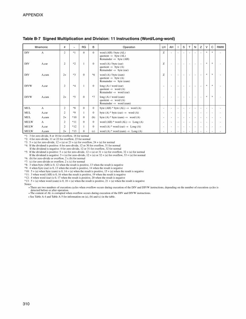
APPENDIX
Table B-7 Signed Multiplication and Division: 11 Instructions (Word/Long-word)
Mnemonic # ~ RG B Operation LH AH I S T N Z V C RMW
DIV A 2 *1 0 0 word (AH) / byte (AL)quotient → byte (AL) Remainder → byte (AH)
Z - - - - - - * * -
DIV A,ear 2 *2 1 0 word (A) / byte (ear)quotient → byte (A) Remainder → byte (ear)
Z - - - - - - * * -
DIV A,eam 2+ *3 0 *6 word (A) / byte (eam)quotient → byte (A) Remainder → byte (eam)
Z - - - - - - * * -
DIVW A,ear 2 *4 1 0 long (A) / word (ear)quotient → word (A) Remainder → word (ear)
- - - - - - - * * -
DIVW A,eam 2+ *5 0 *7 long (A) / word (eam)quotient → word (A) Remainder → word (eam)
- - - - - - - * * -
MUL A 2 *8 0 0 byte (AH) * byte (AL) → word (A) - - - - - - - - - -
MUL A,ear 2 *9 1 0 byte (A) * byte (ear) → word (A) - - - - - - - - - -
MUL A,eam 2+ *10 0 (b) byte (A) * byte (eam) → word (A) - - - - - - - - - -
MULW A 2 *11 0 0 word (AH) * word (AL) → Long (A) - - - - - - - - - -
MULW A,ear 2 *12 1 0 word (A) * word (ear) → Long (A) - - - - - - - - - -
MULW A,eam 2+ *13 0 (c) word (A) * word (eam) → Long (A) - - - - - - - - - -
*1: 3 for zero-divide, 8 or 18 for overflow, 18 for normal*2: 4 for zero-divide, 11 or 22 for overflow, 23 for normal*3: 5 + (a) for zero-divide, 12 + (a) or 23 + (a) for overflow, 24 + (a) for normal*4: If the dividend is positive: 4 for zero-divide, 12 or 30 for overflow, 31 for normal
If the dividend is negative: 4 for zero-divide, 12 or 31 for overflow, 32 for normal*5: If the dividend is positive: 5 + (a) for zero-divide, 12 + (a) or 31 + (a) for overflow, 32 + (a) for normal
If the dividend is negative: 5 + (a) for zero-divide, 12 + (a) or 32 + (a) for overflow, 33 + (a) for normal*6: (b) for zero-divide or overflow, 2 x (b) for normal*7: (c) for zero-divide or overflow, 2 x (c) for normal*8: 3 when byte (AH) is 0, 12 when the result is positive, 13 when the result is negative*9: 4 when byte (ear) is 0, 13 when the result is positive, 14 when the result is negative*10: 5 + (a) when byte (eam) is 0, 14 + (a) when the result is positive, 15 + (a) when the result is negative*11: 3 when word (AH) is 0, 16 when the result is positive, 19 when the result is negative*12: 4 when word (ear) is 0, 17 when the result is positive, 20 when the result is negative*13: 5 + (a) when word (eam) is 0, 18 + (a) when the result is positive, 21 + (a) when the result is negativeNotes:
• There are two numbers of execution cycles when overflow occurs during execution of the DIV and DIVW instructions, depending on the number of execution cycles is detected before or after operation.
• The content of AL is corrupted when overflow occurs during execution of the DIV and DIVW instructions.• See Table A-4 and Table A-5 for information on (a), (b) and (c) in the table.
310

APPENDIX B F2MC-16LX Instruction Lists (351 Instructions)
B.3 Logical Data Operation Instruction
The logical data operation instructions of the F2MC-16L are listed in the following four tables:• Table B-8 for logic 1 (Byte/Word): 39 instructions• Table B-9 for logic 2 (Long): 6 instructions• Table B-10 for sign inversion (Byte/Word): 6 instructions• Table B-11 for normalize instructions (Long): 1 instruction
■ Logical Operation Instruction
Table B-8 Logic 1 (Byte/Word): 39 Instructions (1 / 2)
Mnemonic # ~ RG B Operation LH AH I S T N Z V C RMW
AND A,#imm8 2 2 0 0 byte (A) ← (A) and imm8 - - - - - * * R - -
AND A,ear 2 3 1 0 byte (A) ← (A) and (ear) - - - - - * * R - -
AND A,eam 2+ 4+(a) 0 (b) byte (A) ← (A) and (eam) - - - - - * * R - -
AND ear,A 2 3 2 0 byte (ear) ← (ear) and (A) - - - - - * * R - -
AND eam,A 2+ 5+(a) 0 2 × (b) byte (eam) ← (eam) and (A) - - - - - * * R - *
OR A,#imm8 2 2 0 0 byte (A) ← (A) or imm8 - - - - - * * R - -
OR A,ear 2 3 1 0 byte (A) ← (A) or (ear) - - - - - * * R - -
OR A,eam 2+ 4+(a) 0 (b) byte (A) ← (A) or (eam) - - - - - * * R - -
OR ear,A 2 3 2 0 byte (ear) ← (ear) or (A) - - - - - * * R - -
OR eam,A 2+ 5+(a) 0 2 × (b) byte (eam) ← (eam) or (A) - - - - - * * R - *
XOR A,#imm8 2 2 0 0 byte (A) ← (A) xor imm8 - - - - - * * R - -
XOR A,ear 2 3 1 0 byte (A) ← (A) xor (ear) - - - - - * * R - -
XOR A,eam 2+ 4+(a) 0 (b) byte (A) ← (A) xor (eam) - - - - - * * R - -
XOR ear,A 2 3 2 0 byte (ear) ← (ear) xor (A) - - - - - * * R - -
XOR eam,A 2+ 5+(a) 0 2 × (b) byte (eam) ← (eam) xor (A) - - - - - * * R - *
NOT A 1 2 0 0 byte (A) ← not (A) - - - - - * * R - -
NOT ear 2 3 2 0 byte (ear) ← not (ear) - - - - - * * R - -
NOT eam 2+ 5+(a) 0 2 × (b) byte (eam) ← not (eam) - - - - - * * R - *
ANDW A 1 2 0 0 word (A) ← (AH) and (A) - - - - - * * R - -
ANDW A,#imm16 3 2 0 0 word (A) ← (A) and imm16 - - - - - * * R - -
ANDW A,ear 2 3 1 0 word (A) ← (A) and (ear) - - - - - * * R - -
ANDW A,eam 2+ 4+(a) 0 (c) word (A) ← (A) and (eam) - - - - - * * R - -
ANDW ear,A 2 3 2 0 word (ear) ← (ear) and (A) - - - - - * * R - -
ANDW eam,A 2+ 5+(a) 0 2 × (c) word (eam) ← (eam) and (A) - - - - - * * R - *
ORW A 1 2 0 0 word (A) ← (AH) or (A) - - - - - * * R - -
ORW A,#imm16 3 2 0 0 word (A) ← (A) or imm16 - - - - - * * R - -
ORW A,ear 2 3 1 0 word (A) ← (A) or (ear) - - - - - * * R - -
ORW A,eam 2+ 4+(a) 0 (c) word (A) ← (A) or (eam) - - - - - * * R - -
ORW ear,A 2 3 2 0 word (ear) ← (ear) or (A) - - - - - * * R - -
ORW eam,A 2+ 5+(a) 0 2 × (c) word (eam) ← (eam) or (A) - - - - - * * R - *
311

APPENDIX
XORW A 1 2 0 0 word (A) ← (AH) xor (A) - - - - - * * R - -
XORW A,#imm16 3 2 0 0 word (A) ← (A) xor imm16 - - - - - * * R - -
XORW A,ear 2 3 1 0 word (A) ← (A) xor (ear) - - - - - * * R - -
XORW A,eam 2+ 4+(a) 0 (c) word (A) ← (A) xor (eam) - - - - - * * R - -
XORW ear,A 2 3 2 0 word (ear) ← (ear) xor (A) - - - - - * * R - -
XORW eam,A 2+ 5+(a) 0 2 × (c) word (eam) ← (eam) xor (A) - - - - - * * R - *
NOTW A 1 2 0 0 word (A) ← not (A) - - - - - * * R - -
NOTW ear 2 3 2 0 word (ear) ← not (ear) - - - - - * * R - -
NOTW eam 2+ 5+(a) 0 2 × (c) word (eam) ← not (eam) - - - - - * * R - *
Note: See Table A-4 and Table A-5 for information on (a), (b) and (c) in the table.
Table B-8 Logic 1 (Byte/Word): 39 Instructions (2 / 2)
Mnemonic # ~ RG B Operation LH AH I S T N Z V C RMW
Table B-9 Logic 2 (Long): 6 Instructions
Mnemonic # ~ RG B Operation LH AH I S T N Z V C RMW
ANDL A,ear 2 6 2 0 long (A) ← (A) and (ear) - - - - - * * R - -
ANDL A,eam 2+ 7+(a) 0 (d) long (A) ← (A) and (eam) - - - - - * * R - -
ORL A,ear 2 6 2 0 long (A) ← (A) or (ear) - - - - - * * R - -
ORL A,eam 2+ 7+(a) 0 (d) long (A) ← (A) or (eam) - - - - - * * R - -
XORL A,ear 2 6 2 0 long (A) ← (A) xor (ear) - - - - - * * R - -
XORL A,eam 2+ 7+(a) 0 (d) long (A) ← (A) xor (eam) - - - - - * * R - -
Note: See Table A-4 and Table A-5 for information on (a) and (d) in the table.
Table B-10 Sign Inversion (Byte/Word): 6 Instructions
Mnemonic # ~ RG B Operation LH AH I S T N Z V C RMW
NEG A 1 2 0 0 byte (A) ← 0 - (A) X - - - - * * * * -
NEG ear 2 3 2 0 byte (ear) ← 0 - (ear) - - - - - * * * * -
NEG eam 2+ 5+(a) 0 2 × (b) byte (eam) ← 0 - (eam) - - - - - * * * * *
NEGW A 1 2 0 0 word (A) ← 0 - (A) - - - - - * * * * -
NEGW ear 2 3 2 0 word (ear) ← 0 - (ear) - - - - - * * * * -
NEGW eam 2+ 5+(a) 0 2 × (c) word (eam) ← 0 - (eam) - - - - - * * * * *
Note: See Table A-4 and Table A-5 for information on (a), ( b) and (c) in the table.
Table B-11 Normalize Instruction (Long): 1 Instruction
Mnemonic # ~ RG B Operation LH AH I S T N Z V C RMW
NRML A,R0 2 *1 1 0 long (A) ← Shift to the first bit which is set to 1 formerly placed
byte (R0) ← Number of shifts at that time
- - - - - - * - - -
*1: 4 when all accumulators have a value of 0; otherwise, 6+(R0)Note: See Table A-3 and Table A-4 for information on (a), ( b) and (c) in the table.
312

APPENDIX B F2MC-16LX Instruction Lists (351 Instructions)
B.4 Shift Instruction
Table B-12 lists 18 shift instructions of F2MC-16L.
■ Shift Instruction
Table B-12 Shift Instructions (Byte/Word/Long-word): 18 Instructions
Mnemonic # ~ RG B Operation LH AH I S T N Z V C RMW
RORC A 2 2 0 0 byte (A) ← Right rotate with carry - - - - - * * - * -
ROLC A 2 2 0 0 byte (A) ← Left rotate with carry - - - - - * * - * -
RORC ear 2 3 2 0 byte (ear) ← Right rotate with carry - - - - - * * - * -
RORC eam 2+ 5+(a) 0 2 × (b) byte (eam) ← Right rotate with carry - - - - - * * - * *
ROLC ear 2 3 2 0 byte (ear) ← Left rotate with carry - - - - - * * - * -
ROLC eam 2+ 5+(a) 0 2 × (b) byte (eam) ← Left rotate with carry - - - - - * * - * *
ASR A,R0 2 *1 1 0 byte (A) ← Arithmetic right shift (A, R0) - - - - * * * - * -
LSR A,R0 2 *1 1 0 byte (A) ← Logical right barrel shift (A, R0) - - - - * * * - * -
LSL A,R0 2 *1 1 0 byte (A) ← Logical left barrel shift (A, R0) - - - - - * * - * -
ASRW A 1 2 0 0 word (A) ← Arithmetic right shift (A, 1 bit) - - - - * * * - * -
LSRW A/SHRW A 1 2 0 0 word (A) ← Logical right shift (A, 1 bit) - - - - * R * - * -
LSLW A/SHLW A 1 2 0 0 word (A) ← Logical left shift (A, 1 bit) - - - - - * * - * -
ASRW A,R0 2 *1 1 0 word (A) ← Arithmetic right barrel shift (A, R0) - - - - * * * - * -
LSRW A,R0 2 *1 1 0 word (A) ← Logical right barrel shift (A, R0) - - - - * * * - * -
LSLW A,R0 2 *1 1 0 word (A) ← Logical left barrel shift (A, R0) - - - - - * * - * -
ASRL A,R0 2 *2 1 0 long (A) ← Arithmetic right barrel shift (A, R0) - - - - * * * - * -
LSRL A,R0 2 *2 1 0 long (A) ← Logical right barrel shift (A, R0) - - - - * * * - * -
LSLL A,R0 2 *2 1 0 long (A) ← Logical left barrel shift (A, R0) - - - - - * * - * -
*1: 6 when R0 is 0; otherwise, 5 + (R0)*2: 6 when R0 is 0; otherwise, 6 + (R0)Note: See Table A-4 and Table A-5 for information on (a) and (b) in the table.
313

APPENDIX
B.5 Branch Instructions
The branch instructions of the F2MC-16L are listed in the following two tables:• Table B-13 for branch 1: 31 instructions• Table B-14 for branch 2: 19 instructions
■ Branch Instruction
Table B-13 Branch 1: 31 Instructions
Mnemonic # ~ RG B Operation LH AH I S T N Z V C RMW
BZ/BEQ rel 2 *1 0 0 Branch on (Z) = 1 - - - - - - - - - -
BNZ/BNE rel 2 *1 0 0 Branch on (Z) = 0 - - - - - - - - - -
BC/BLO rel 2 *1 0 0 Branch on (C) = 1 - - - - - - - - - -
BNC/BHS rel 2 *1 0 0 Branch on (C) = 0 - - - - - - - - - -
BN rel 2 *1 0 0 Branch on (N) = 1 - - - - - - - - - -
BP rel 2 *1 0 0 Branch on (N) = 0 - - - - - - - - - -
BV rel 2 *1 0 0 Branch on (V) = 1 - - - - - - - - - -
BNV rel 2 *1 0 0 Branch on (V) = 0 - - - - - - - - - -
BT rel 2 *1 0 0 Branch on (T) = 1 - - - - - - - - - -
BNT rel 2 *1 0 0 Branch on (T) = 0 - - - - - - - - - -
BLT rel 2 *1 0 0 Branch on (V) xor (N) = 1 - - - - - - - - - -
BGE rel 2 *1 0 0 Branch on (V) xor (N) = 0 - - - - - - - - - -
BLE rel 2 *1 0 0 Branch on ((V) xor (N)) or (Z) = 1 - - - - - - - - - -
BGT rel 2 *1 0 0 Branch on ((V) xor (N)) or (Z) = 0 - - - - - - - - - -
BLS rel 2 *1 0 0 Branch on (C) or (Z) = 1 - - - - - - - - - -
BHI rel 2 *1 0 0 Branch on (C) or (Z) = 0 - - - - - - - - - -
BRA rel 2 *1 0 0 Unconditional branch - - - - - - - - - -
JMP @A 1 2 0 0 word (PC) ← (A) - - - - - - - - - -
JMP addr16 3 3 0 0 word (PC) ← addr16 - - - - - - - - - -
JMP @ear 2 3 1 0 word (PC) ← (ear) - - - - - - - - - -
JMP @eam 2+ 4+(a) 0 (c) word (PC) ← (eam) - - - - - - - - - -
JMPP @ear *3 2 5 2 0 word (PC) ← (ear), (PCB) ← (ear+2) - - - - - - - - - -
JMPP @eam *3 2+ 6+(a) 0 (d) word (PC) ← (eam), (PCB) ← (eam+2) - - - - - - - - - -
JMPP addr24 4 4 0 0 word (PC) ← ad24 0-15, (PCB) ← ad24 16-23 - - - - - - - - - -
CALL @ear *4 2 6 1 (c) word (PC) ← (ear) - - - - - - - - - -
CALL @eam *4 2+ 7+(a) 0 2 × (c) word (PC) ← (eam) - - - - - - - - - -
CALL addr16 *5 3 6 0 (c) word (PC) ← addr16 - - - - - - - - - -
CALLV #vct4 *5 1 7 0 2 × (c) Vector call instruction - - - - - - - - - -
CALLP @ear *6 2 10 2 2 × (c) word (PC) ← (ear)0-15, (PCB) ← (ear)16-23 - - - - - - - - - -
CALLP @eam *6 2+ 11+(a) 0 *2 word (PC) ← (eam)0-15, (PCB) ← (eam)16-23 - - - - - - - - - -
CALLP addr24 *7 4 10 0 2 × (c) word (PC) ← addr0-15, (PCB) ← addr16-23 - - - - - - - - - -
*1: 4 when branch is made, 6 when branch is not made*2: 3 × (c) + (b)*3: Read the branched address (word)*4: W: Save to stack (word), R: Read the branched address (word)*5: Save to stack (word)*6: W: Save to stack (long), R: Read the branched address (long)*7: Save to stack (long)Note: See Table A-4 and for information on (a) to (d) in the table.
314

APPENDIX B F2MC-16LX Instruction Lists (351 Instructions)
Table B-14 Branch 2: 19 Instructions
Mnemonic # ~ RG B Operation LH AH I S T N Z V C RMW
CBNE A,#imm8,rel 3 *1 0 0 Branch on byte (A) not equal to imm8 - - - - - * * * * -
CWBNE A,#imm16,rel 4 *1 0 0 Branch on word (A) not equal to imm16 - - - - - * * * * -
CBNE ear,#imm8,rel 4 *2 1 0 Branch on byte (ear) not equal to imm8 - - - - - * * * * -
CBNE eam,#imm8,rel *9 4+ *3 0 (b) Branch on byte (eam) not equal to imm8 - - - - - * * * * -
CWBNE ear,#imm16,rel 5 *4 1 0 Branch on word (ear) not equal to imm16 - - - - - * * * * -
CWBNE eam,#imm16,rel*9 5+ *3 0 (c) Branch on word (eam) not equal to imm16 - - - - - * * * * -
DBNZ ear,rel 3 *5 2 0 Branch on byte (ear) = (ear) - 1, (ear) not equal to 0 - - - - - * * * - -
DBNZ eam,rel 3+ *6 2 2 × (b) Branch on byte (eam) = (eam) - 1, (eam) not equal to 0 - - - - - * * * - *
DWBNZ ear,rel 3 *5 2 0 Branch on word (ear) = (ear) - 1, (ear) not equal to 0 - - - - - * * * - -
DWBNZ eam,rel 3+ *6 2 2 × (c) Branch on word (eam) = (eam) - 1, (eam) not equal to 0 - - - - - * * * - *
INT #vct8 2 20 0 8 × (c) Software interrupt - - R S - - - - - -
INT addr16 3 16 0 6 × (c) Software interrupt - - R S - - - - - -
INTP addr24 4 17 0 6 × (c) Software interrupt - - R S - - - - - -
INT9 1 20 0 8 × (c) Software interrupt - - R S - - - - - -
RETI 1 *8 0 *7 Return from interrupt - - * * * * * * * -
LINK #imm8 2 6 0 (c) At the entrance of function, save old frame pointers im stack, set up new frame pointers, reserve area for local pointers.
- - - - - - - - - -
UNLINK 1 5 0 (c) At the exit of function, recover the old frame pointers from the stack.
- - - - - - - - - -
RET *10 1 4 0 (c) Return from subroutine - - - - - - - - - -
RETP *11 1 6 0 (d) Return from subroutine - - - - - - - - - -
*1: 5 when branch is made, 4 when branch is not made*2: 13 when branch is made, 12 when branch is not made*3: 7 + (a) when branch is made, 6 + (a) when branch is not made*4: 8 when branch is made, 7 when branch is not made*5: 7 when branch is made, 6 when branch is not made*6: 8 + (a) when branch is made, 7 + (a) when branch is not made*7: 3 × (b) + 2 × (c) when the sequence is branched to the next interrupt request, 6 × (c) when returned from the current interruption*8: 15 when the sequence is branched to the next interrupt request, 17 when returned from the current interruption*9: Do not use the RWj + addressing mode for the CBNE/CWBNE instruction.*10: Return from stack (word)*11: Return from stack (long)Note: See Table A-5 and Table A-5 for information on (a) to (d) in the table.
315

APPENDIX
B.6 Other Instructions
Other instructions of the F2MC-16L are listed in the following four tables:• Table B-15 for other control systems (Byte/Word/Long-word) : 28 instructions• Table B-16 for bit operation instructions: 21 instructions• Table B-17 for accumulator operation instructions (Byte/Word): 6 instructions• Table B-18 for string instructions: 10 instructions
■ Other Instructions
Table B-15 Other Control Systems (Byte/Word/Long-word): 28 Instructions
Mnemonic # ~ RG B Operation LH AH I S T N Z V C RMW
PUSHW A 1 4 0 (c) word (SP) ← (SP) - 2, ((SP)) ← (A) - - - - - - - - - -
PUSHW AH 1 4 0 (c) word (SP) ← (SP) - 2, ((SP)) ← (AH) - - - - - - - - - -
PUSHW PS 1 4 0 (c) word (SP) ← (SP) - 2, ((SP)) ← (PS) - - - - - - - - - -
PUSHW rlst 2 *3 *5 *4 (SP) ← (SP) - 2n, ((SP)) ← (rlst) - - - - - - - - - -
POPW A 1 3 0 (c) word (A) ← ((SP)), (SP) ← (SP) + 2 - * - - - - - - - -
POPW AH 1 3 0 (c) word (AH) ← ((SP)), (SP) ← (SP) + 2 - - - - - - - - - -
POPW PS 1 4 0 (c) word (PS) ← ((SP)), (SP) ← (SP) + 2 - - * * * * * * * -
POPW rlst 2 *2 *5 *4 (rlst) ← ((SP)), (SP) ← (SP) - - - - - - - - - -
JCTX @A 1 14 0 6 × (c) Context switching instruction - - * * * * * * * -
AND CCR,#imm8 2 3 0 0 byte (CCR) ← (CCR) and imm8 - - * * * * * * * -
OR CCR,#imm8 2 3 0 0 byte (CCR) ← (CCR) or imm8 - - * * * * * * * -
MOV RP,#imm8 2 2 0 0 byte (RP) ← imm8 - - - - - - - - - -
MOV ILM,#imm8 2 2 0 0 byte (ILM) ← imm8 - - - - - - - - - -
MOVEA RWi,ear 2 3 1 0 word (RWi) ← ear - - - - - - - - - -
MOVEA RWi,eam 2+ 2+(a) 1 0 word (RWi) ← eam - - - - - - - - - -
MOVEA A,ear 2 1 0 0 word (A) ← ear - * - - - - - - - -
MOVEA A,eam 2+ 1+(a) 0 0 word (A) ← eam - * - - - - - - - -
ADDSP #imm8 2 3 0 0 word (SP) ← ext(imm8) - - - - - - - - - -
ADDSP #imm16 3 3 0 0 word (SP) ← imm16 - - - - - - - - - -
MOV A,brg1 2 *1 0 0 byte (A) ← (brg1) Z * - - - * * - - -
MOV brg2,A 2 1 0 0 byte (brg2) ← (A) - - - - - * * - - -
NOP 1 1 0 0 No operation - - - - - - - - - -
ADB 1 1 0 0 Prefix code for AD space access - - - - - - - - - -
DTB 1 1 0 0 Prefix code for DT space access - - - - - - - - - -
PCB 1 1 0 0 Prefix code for PC space access - - - - - - - - - -
SPB 1 1 0 0 Prefix code for SP space access - - - - - - - - - -
NCC 1 1 0 0 Prefix code for flag unchange setting - - - - - - - - - -
CMR 1 1 0 0 Prefix for common register banks - - - - - - - - - -
*1: 1 for PCB, ADB, SSB, USB, and SPB 2 for DTB and DPR*2: 7 + 3 × (number of POP operations) + 2 × (number of the last register that operates POP), 7 when RLST = 0 (no transfer register)*3: 29 + 3 × (number of PUSH operations) - 3 × (number of the last register that operates PUSH), 8 when RLST = 0 (no transfer register)*4: (number of POP operations) × c, or (number of PUSH operations) × c*5: (number of POP operations), or (number of PUSH operations)Note: See Table A-4 and Table A-5 for information on (a) and (c) in the table.
316

APPENDIX B F2MC-16LX Instruction Lists (351 Instructions)
Table B-16 Bit Operation Instruction: 21 Instructions
Mnemonic # ~ RG B Operation LH AH I S T N Z V C RMW
MOVB A,dir:bp 3 5 0 (b) byte (A) ← (dir:bp)b Z * - - - * * - - -
MOVB A,addr16:bp 4 5 0 (b) byte (A) ← (addr16:bp)b Z * - - - * * - - -
MOVB A,io:bp 3 4 0 (b) byte (A) ← (io:bp)b Z * - - - * * - - -
MOVB dir:bp,A 3 7 0 2 × (b) bit (dir:bp)b ← (A) - - - - - * * - - *
MOVB addr16:bp,A 4 7 0 2 × (b) bit (addr16:bp)b ← (A) - - - - - * * - - *
MOVB io:bp,A 3 6 0 2 × (b) bit (io:bp)b ← (A) - - - - - * * - - *
SETB dir:bp 3 7 0 2 × (b) bit (dir:bp)b ← 1 - - - - - - - - - *
SETB addr16:bp 4 7 0 2 × (b) bit (addr16:bp)b ← 1 - - - - - - - - - *
SETB io:bp 3 7 0 2 × (b) bit (io:bp)b ← 1 - - - - - - - - - *
CLRB dir:bp 3 7 0 2 × (b) bit (dir:bp)b ← 0 - - - - - - - - - *
CLRB addr16:bp 4 7 0 2 × (b) bit (addr16:bp)b ← 0 - - - - - - - - - *
CLRB io:bp 3 7 0 2 × (b) bit (io:bp)b ← 0 - - - - - - - - - *
BBC dir:bp,rel 4 *1 0 (b) Branch on (dir:bp) b = 0 - - - - - - * - - -
BBC addr16:bp,rel 5 *1 0 (b) Branch on (addr16:bp) b = 0 - - - - - - * - - -
BBC io:bp,rel 4 *2 0 (b) Branch on (io:bp) b = 0 - - - - - - * - - -
BBS dir:bp,rel 4 *1 0 (b) Branch on (dir:bp) b = 1 - - - - - - * - - -
BBS addr16:bp,rel 5 *1 0 (b) Branch on (addr16:bp) b = 1 - - - - - - * - - -
BBS io:bp,rel 4 *2 0 (b) Branch on (io:bp) b = 1 - - - - - - * - - -
SBBS addr16:bp,rel 5 *3 0 2 × (b) Branch on (addr16:bp) b = 1, bit = 1 - - - - - - * - - *
WBTS io:bp 3 *4 0 *5 Waits until (io:bp) b = 1 - - - - - - - - - -
WBTC io:bp 3 *4 0 *5 Waits until (io:bp) b = 0 - - - - - - - - - -
*1: 8 when branch is made, 7 when branch is not made*2: 7 when branch is made, 6 when branch is not made*3: 10 when the condition is met, 9 when the condition is not met*4: Undefined count*5: Until the condition is metNote: See Table A-5 for information on (b) in the table.
Table B-17 Accumulator Operation Instruction (Byte/Word): 6 Instructions
Mnemonic # ~ RG B Operation LH AH I S T N Z V C RMW
SWAP 1 3 0 0 byte (A)0-7 ↔ (A)8-15 - - - - - - - - - -
SWAPW 1 2 0 0 word (AH) ↔ (AL) - * - - - - - - - -
EXT 1 1 0 0 Byte signed extension X - - - - * * - - -
EXTW 1 2 0 0 Word signed extension - X - - - * * - - -
ZEXT 1 1 0 0 Byte zero extension Z - - - - R * - - -
ZEXTW 1 1 0 0 Word zero extension - Z - - - R * - - -
317

APPENDIX
Table B-18 String Instruction : 10 Instructions
Mnemonic # ~ RG B Operation LH AH I S T N Z V C RMW
MOVS / MOVSI 2 *2 *5 *3 byte transfer @AH+ ← @AL+, counter = RW0 - - - - - - - - - -
MOVSD 2 *2 *5 *3 byte transfer @AH- ← @AL-, counter = RW0 - - - - - - - - - -
SCEQ / SCEQI 2 *1 *8 *4 byte search @AH+ ← AL, counter RW0 - - - - - * * * * -
SCEQD 2 *1 *8 *4 byte search @AH- ← AL, counter RW0 - - - - - * * * * -
FILS / FILSI 2 6m+6 *8 *3 byte fill @AH+ ← AL, counter RW0 - - - - - * * - - -
MOVSW / MOVSWI 2 *2 *5 *6 word transfer @AH+ ← @AL+, counter = RW0 - - - - - - - - - -
MOVSWD 2 *2 *5 *6 word transfer @AH- ← @AL-, counter = RW0 - - - - - - - - - -
SCWEQ / SCWEQI 2 *1 *8 *7 word search @AH+ - AL, counter = RW0 - - - - - * * * * -
SCWEQD 2 *1 *8 *7 word search @AH- - AL, counter = RW0 - - - - - * * * * -
FILSW / FILSWI 2 6m+6 *8 *6 word fill @AH+ ← AL, counter = RW0 - - - - - * * - - -
*1: 5 when RW0 is 0, 4 + 7 × (RW0) when count-out is detected, and 7n + 5 when the data in the AL register matches the byte data specified by the AH register in the space that is specified by bank
*2: 5 when RW0 is 0, 4 + 8 × (RW0) for otherwise*3: (b) × (RW0) + (b) × (RW0):To access different areas for sources and destinations, calculate item (b) separately each other.*4: (b) × n*5: 2 × (b) × (RW0)*6: (c) × (RW0) + (c) × (RW0):To access different areas for sources and destinations, calculate item (c) separately each other.*7: (c) × n*8: (b) × (RW0)
Notes: • m: RW0 value (counter value), n: Number of loops
• See Table A-5 for information on (b) and (c) in the table.
318

APPENDIX C F2MC-16LX Instruction Maps
APPENDIX C F2MC-16LX Instruction Maps
This appendix describes F2MC-16LX instruction maps.
C.1 Structure of the Instruction Map
C.2 Basic Page Map
C.3 Bit Operation Instruction Map
C.4 Character String Operation Instruction Map
C.5 2-byte Instruction Map
C.6 ea-type Instruction Map
C.7 MOVEA RWi, ea Instruction Map
C.8 MOV Ri, ea Instruction Map
C.9 MOVW RWi, ea Instruction Map
C.10 MOV ea, Ri Instruction Map
C.11 MOVW ea, RWi Instruction Map
C.12 XCH Ri, ea Instruction Map
C.13 XCHW RWi, ea Instruction Map
319
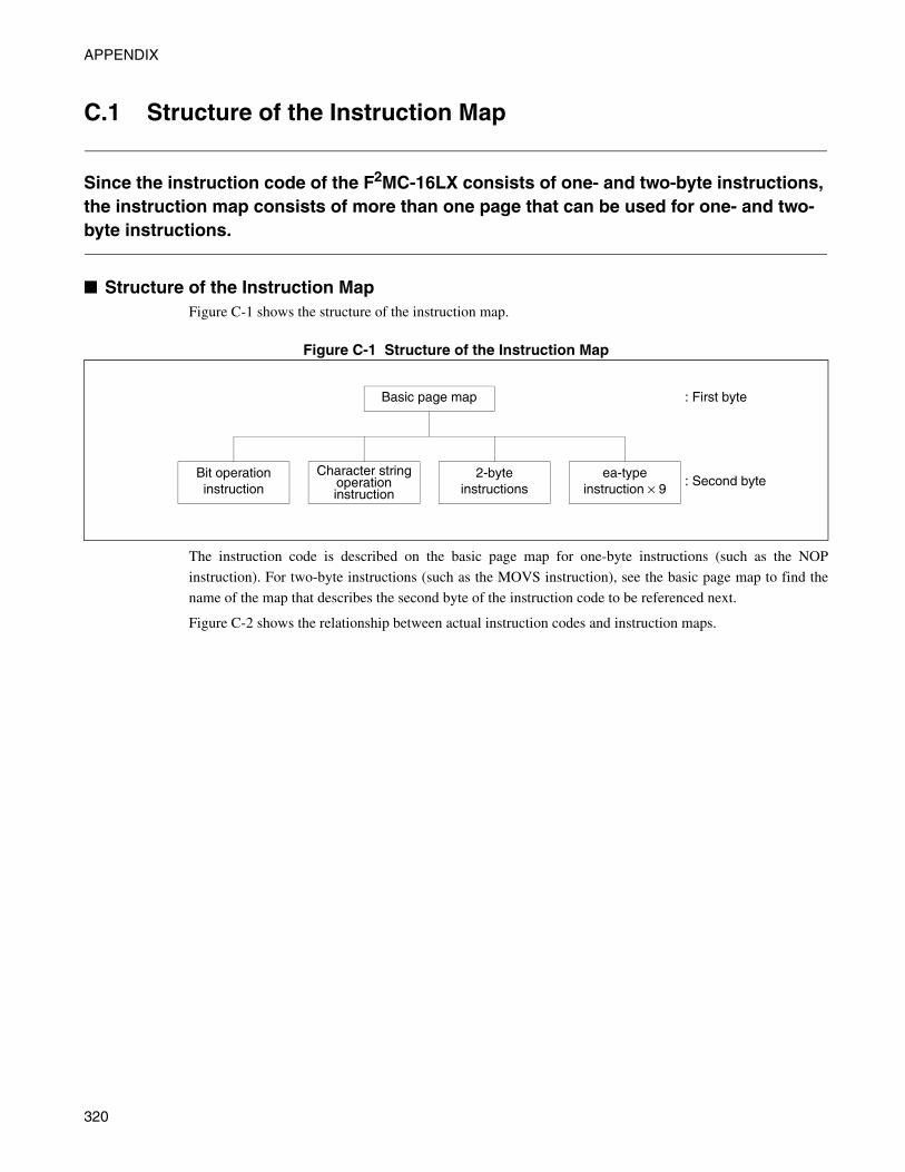
APPENDIX
C.1 Structure of the Instruction Map
Since the instruction code of the F2MC-16LX consists of one- and two-byte instructions, the instruction map consists of more than one page that can be used for one- and two- byte instructions.
■ Structure of the Instruction MapFigure C-1 shows the structure of the instruction map.
Figure C-1 Structure of the Instruction Map
The instruction code is described on the basic page map for one-byte instructions (such as the NOP
instruction). For two-byte instructions (such as the MOVS instruction), see the basic page map to find the
name of the map that describes the second byte of the instruction code to be referenced next.
Figure C-2 shows the relationship between actual instruction codes and instruction maps.
Basic page map : First byte
Bit operation instruction
Character string operation instruction
2-byte instructions
ea-type instruction × 9
: Second byte
320

APPENDIX C F2MC-16LX Instruction Maps
Figure C-2 Relationship Between Actual Instruction Codes and Instruction Maps
*: Extended page map is a generic name for bit operation instruction, character stringoperation instruction, 2-byte instruction, and ea-type instruction. More than one extendedpage map exists for each type of instruction.
May not exist for some instruction.
The length varies depending on instructions.
Instruction code
First byte Second byte Operand Operand . . .
[Basic page map]
XY
+Z
[Extended page map]*
UV
+W
321

APPENDIX
C.2 Basic Page Map
Table C-1 shows the basic page map.
■ Basic Page Map
322

APPENDIX C F2MC-16LX Instruction Maps
Table C-1 Basic Page Map
Note: For the information about ea-type instruction from (1) to (9), see Table C.6,"ea-type Instruction".
0010
2030
4050
6070
8090
A0
B0
C0
D0
E0
F0
+0
NO
PC
MR
AD
DA
, dir
AD
DA
, #8
MO
VA
, dir
MO
VA
, io
BR
Are
lea
inst
ruct
ion
1M
OV
A, R
iMO
VR
i, A
MO
VR
i, #8
MO
VA
, RiM
OV
X A
,@
RW
i+d8
MO
VA
, #4
CA
LL#4
BZ
/BE
Qre
l
+1
INT
9N
CC
SU
BA
, dir
SU
BA
, #8
MO
Vdi
r, A
MO
Vio
, AJM
P@
Aea
in
stru
ctio
n 2
BN
Z/B
NE re
l
+2
AD
DD
CA
SU
BD
CA
AD
DC
AS
UB
CA
MO
VA
, #8
MO
VA
, add
r16
JMP
addr
16ea
in
stru
ctio
n 3
BC
/BL0
rel
+3
NE
GA
JCT
X@
AC
MP
AC
MP
A, #
8M
OV
XA
, #8
MO
Vad
dr16
, AJM
PP ad
de24
ea
inst
ruct
ion
4B
NC
/BH
S rel
+4
PC
BE
XT
AN
D CC
R, #
8A
ND
A, #
8M
OV
dir,
#8
MO
Vio
, #8
CA
LLad
dr16
ea
inst
ruct
ion
5B
Nre
l
+5
DT
BZ
EX
TO
RC
CR
, #8
OR
A, #
8M
OV
XA
, dir
MO
VX
A, i
oC
ALL
P addr
24ea
in
stru
ctio
n 6
BP
rel
+6
AD
BS
WA
PD
IVU
AX
OR
A, #
8M
OV
W A, S
PM
OV
W io, #
16R
ET
Pea
in
stru
ctio
n 7
BV
rel
+7
SP
BA
DD
SP
#8M
ULU
AN
OT
AM
OV
W SP
, AM
OV
XA
, add
r16
RE
Tea
in
stru
ctio
n 8
BN
Vre
l
+8
LIN
K#i
mm
8A
DD
L A, #
32A
DD
WA
AD
DW A
, #16
MO
VW
A, d
irM
OV
WA
, io
INT
#vct
8ea
in
stru
ctio
n 9
MO
VW A
, RW
iMO
VW R
Wi,
AM
OV
WR
Wi,
#16
MO
V A
,@
RW
i+d8
MO
VW
@R
Wi+
d8, A
BT
rel
+9
UN
LIN
KS
UB
L A, #
32S
UB
WA
SU
BW A
, #16
MO
VW
dir,
AM
OV
Wio
, AIN
Tad
dr16
MO
VE
AR
Wi,
eaB
NT
rel
+A
MO
V RP
, #8
MO
V ILM
, #8
CB
NE
A,
#8, r
elC
WB
NE
A,
#16,
rel
MO
VW A
, #16
MO
VW
A,a
ddr1
6IN
TP ad
dr24
MO
VR
i, ea
BLT
rel
+B
NE
GW
AC
MP
L A, #
32C
MP
WA
CM
PW A
, #16
MO
VL A
, #32
MO
VW
addr
16, A
RE
TI
MO
VW
RW
i, ea
BG
Ere
l
+C
LSLW
AE
XT
WA
ND
WA
AN
DW A
, #16
PU
SH
WA
PO
PW
AB
it op
erat
ion
inst
ruct
ion
MO
Vea
, Ri
BLE
rel
+D
ZE
XT
WO
RW
AO
RW
A, #
16P
US
HW
AH
PO
PW
AH
MO
VW
ea, R
Wi
BG
Tre
l
+E
AS
RW
AS
WA
PW
XO
RW
AX
OR
W A, #
16P
US
HW
PS
PO
PW
PS
Cha
ract
er s
tring
op
erat
ion
inst
ruct
ion
XC
HR
i, ea
BLS
rel
+F
LSR
WA
AD
DS
P#1
6M
ULU
WA
NO
TW
AP
US
HW
rlstP
OP
Wrls
t2-by
te
inst
ruct
ion
XC
HW RW
i, ea
BH
Ire
l
323
APPENDIX
C.3 Bit Operation Instruction Map
Table C-2 shows the bit operation instruction map.
324

APPENDIX C F2MC-16LX Instruction Maps
■ Bit Operation Instruction MapTable C-2 Bit Operation Instruction Map (First Byte = 6CH)
0010
2030
4050
6070
8090
A0
B0
C0
D0
E0
F0
+0
MO
VB
A, i
o:bp
MO
VB
io:b
p, A
CLR
Bio
:bp
SE
TB
io:b
pB
BC io
;bp,
rel
BB
S io:b
p, r
elW
BT
S io:b
pW
BT
C io:b
p
+1
+2
+3
+4
+5
+6
+7
+8
MO
VB
A, d
ir:bp
MO
VB
A,
addr
16:b
pM
OV
Bdi
r:bp
, AM
OV
Bad
dr16
:bp,
AC
LRB di
r:bp
CLR
Bad
dr16
:bp
SE
TB di
r:bp
SE
TB
addr
16:b
pB
BC dir:
bp, r
elB
BC
addr
16:b
p,re
lB
BS dir:
bp, r
elB
BS
addr
16:b
p,re
lS
BB
Sad
dr16
:bp
+9
+A
+B
+C
+D +E +F
325

APPENDIX
C.4 Character String Operation Instruction Map
Table C-3 shows the character string operation instruction map.
326

APPENDIX C F2MC-16LX Instruction Maps
■ Character String Operation Instruction MapTable C-3 Character String Operation Instruction Map (First Byte = 6EH)
0010
2030
4050
6070
8090
A0
B0
C0
D0
E0
F0
+0
MO
VS
IP
CB
, PC
BM
OV
SD
MO
VS
WI
MO
VS
WD
SC
EQ
I PC
BS
CE
QD P
CB
SC
WE
QI
PC
BS
CW
EQ
DP
CB
FIL
SI
PC
BF
ILS
IP
CB
+1
PC
B, D
TB
DT
BD
TB
DT
BD
TB
DT
BD
TB
+2
PC
B, A
DB
AD
BA
DB
AD
BA
DB
AD
BA
DB
+3
PC
B, S
PB
SP
BS
PB
SP
BS
PB
SP
BS
PB
+4
DT
B, P
CB
+5
DT
B, D
TB
+6
DT
B, A
DB
+7
DT
B, S
PB
+8
AD
B, P
CB
+9
AD
B, D
TB
+A
AD
B, A
DB
+B
AD
B, S
PB
+C
SP
B, P
CB
+D
SP
B, D
TB
+E
SP
B, A
DB
+F
SP
B, S
PB
327

APPENDIX
C.5 2-byte Instruction Map
Table C-4 shows the 2-byte instruction map.
328

APPENDIX C F2MC-16LX Instruction Maps
■ 2-byte Instruction MapTable C-4 2-byte Instruction Map (First Byte = 6FH)
0010
2030
4050
6070
8090
A0
B0
C0
D0
E0
F0
+0
MO
V A, D
TB
MO
V DT
B, A
MO
VX
A, @
RL0
+d8
MO
V@
RL0
+d8,
AM
OV
A, @
RL0
+d8
+1
MO
V A, A
DB
MO
V AD
B, A
+2
MO
V A, S
SB
MO
V SS
B, A
MO
VX
A, @
RL1
+d8
MO
V@
RL1
+d8,
AM
OV
A, @
RL1
+d8
+3
MO
V A, U
SB
MO
V US
B, A
+4
MO
V A, D
PR
MO
V DP
R, A
MO
VX
A, @
RL2
+d8
MO
V@
RL2
+d8,
AM
OV
A, @
RL2
+d8
+5
MO
V A, @
AM
OV
@A
L, A
H
+6
MO
V A, P
CB
MO
V A, @
AM
OV
XA
, @R
L3+d
8M
OV
@R
L3+d
8, A
MO
VA
, @R
L3+d
8
+7
RO
LCA
RO
LCA
+8
MO
VW
@R
L0+d
8, A
MO
VW
A, @
RL0
+d8
MU
LA
+9
MU
LWA
+A
MO
VW
@R
L1+d
8, A
MO
VW
A, @
RL1
+d8
DIV
UA
+B
+C
LSLW
A, R
0LS
LLA
, R0
LSL
A, R
0M
OV
W@
RL2
+d8,
AM
OV
WA
, @R
L2+d
8
+D
MO
VW A, @
AM
OV
W@
AL,
AH
NR
ML A
, R0
+E
AS
RW A
, R0
AS
RL A
, R0
AS
RA
, R0
MO
VW
@R
L3+d
8, A
MO
VW
A, @
RL3
+d8
+F
LSR
W A, R
0LS
RL A
, R0
LSR
A, R
0
329

APPENDIX
C.6 ea-type Instruction Map
ea-type instruction maps (first byte = 70H to first byte = 78H) are shown in the following
nine tables:• Table C-5 for ea-type instruction (1) (first byte = 70H)
• Table C-6 for ea-type instruction (2) (first byte = 71H)
• Table C-7 for ea-type instruction (3) (first byte = 72H)
• Table C-8 for ea-type instruction (4) (first byte = 73H)
• Table C-9 for ea-type instruction (5) (first byte = 74H)
• Table C-10 for ea-type instruction (6) (first byte = 75H)
• Table C-11 for ea-type instruction (7) (first byte = 76H)
• Table C-12 for ea-type instruction (8) (first byte = 77H)
• Table C-13 for ea-type instruction (9) (first byte = 78H)
330

APPENDIX C F2MC-16LX Instruction Maps
■ ea-type Instruction MapTable C-5 ea-byte Instruction (1) (First Byte = 70H)
0010
2030
4050
6070
8090
A0
B0
C0
D0
E0
F0
CW
BN
E ↓
CW
BN
E ↓
CB
NE
↓C
BN
E ↓
+0
AD
DL A, R
L0A
DD
L A
,@
RW
0+d8
SU
BL A, R
L0S
UB
L A
,@
RW
0+d8
RW
0,#1
6, r
el@
RW
0+d8
#16,
rel
CM
PL A, R
L0C
MP
L A
,@
RW
0+d8
AN
DL A, R
L0A
ND
L A
,@
RW
0+d8
OR
L A, R
L0O
RL
A,
@R
W0+
d8X
OR
L A, R
L0X
OR
L A
,@
RW
0+d8
R0,
#8, r
el@
RW
0+d8
,#8
, rel
+1
AD
DL A, R
L0A
DD
L A
,@
RW
1+d8
SU
BL A, R
L0S
UB
L A
,@
RW
1+d8
RW
1,#1
6, r
el@
RW
1+d8
#16,
rel
CM
PL A, R
L0C
MP
L A
,@
RW
1+d8
AN
DL A, R
L0A
ND
L A
,@
RW
1+d8
OR
L A, R
L0O
RL
A,
@R
W1+
d8X
OR
L A, R
L0X
OR
L A
,@
RW
1+d8
R1,
#8, r
el@
RW
1+d8
,#8
, rel
+2
AD
DL A, R
L1A
DD
L A
,@
RW
2+d8
SU
BL A, R
L1S
UB
L A
,@
RW
2+d8
RW
2,#1
6, r
el@
RW
2+d8
#16,
rel
CM
PL A, R
L1C
MP
L A
,@
RW
2+d8
AN
DL A, R
L1A
ND
L A
,@
RW
2+d8
OR
L A, R
L1O
RL
A,
@R
W2+
d8X
OR
L A, R
L1X
OR
L A
,@
RW
2+d8
R2,
#8, r
el@
RW
2+d8
,#8
, rel
+3
AD
DL A, R
L1A
DD
L A
,@
RW
3+d8
SU
BL A, R
L1S
UB
L A
,@
RW
3+d8
RW
3,#1
6, r
el@
RW
3+d8
#16,
rel
CM
PL A, R
L1C
MP
L A
,@
RW
3+d8
AN
DL A, R
L1A
ND
L A
,@
RW
3+d8
OR
L A, R
L1O
RL
A,
@R
W3+
d8X
OR
L A, R
L1X
OR
L A
,@
RW
3+d8
R3,
#8, r
el@
RW
3+d8
,#8
, rel
+4
AD
DL A, R
L2A
DD
L A
,@
RW
4+d8
SU
BL A, R
L2S
UB
L A
,@
RW
4+d8
RW
4,#1
6, r
el@
RW
4+d8
#16,
rel
CM
PL A, R
L2C
MP
L A
,@
RW
4+d8
AN
DL A, R
L2A
ND
L A
,@
RW
4+d8
OR
L A, R
L2O
RL
A,
@R
W4+
d8X
OR
L A, R
L2X
OR
L A
,@
RW
4+d8
R4,
#8, r
el@
RW
4+d8
,#8
, rel
+5
AD
DL A, R
L2A
DD
L A
,@
RW
5+d8
SU
BL A, R
L2S
UB
L A
,@
RW
5+d8
RW
5,#1
6, r
el@
RW
5+d8
#16,
rel
CM
PL A, R
L2C
MP
L A
,@
RW
5+d8
AN
DL A, R
L2A
ND
L A
,@
RW
5+d8
OR
L A, R
L2O
RL
A,
@R
W5+
d8X
OR
L A, R
L2X
OR
L A
,@
RW
5+d8
R5,
#8, r
el@
RW
5+d8
,#8
, rel
+6
AD
DL A, R
L3A
DD
L A
,@
RW
6+d8
SU
BL A, R
L3S
UB
L A
,@
RW
6+d8
RW
6,#1
6, r
el@
RW
6+d8
#16,
rel
CM
PL A, R
L3C
MP
L A
,@
RW
6+d8
AN
DL A, R
L3A
ND
L A
,@
RW
6+d8
OR
L A, R
L3O
RL
A,
@R
W6+
d8X
OR
L A, R
L3X
OR
L A
,@
RW
6+d8
R6,
#8, r
el@
RW
6+d8
,#8
, rel
+7
AD
DL A, R
L3A
DD
L A
,@
RW
7+d8
SU
BL A, R
L3S
UB
L A
,@
RW
7+d8
RW
7,#1
6, r
el@
RW
7+d8
#16,
rel
CM
PL A, R
L3C
MP
L A
,@
RW
7+d8
AN
DL A, R
L3A
ND
L A
,@
RW
7+d8
OR
L A, R
L3O
RL
A,
@R
W7+
d8X
OR
L A, R
L3X
OR
L A
,@
RW
7+d8
R7,
#8, r
el@
RW
7+d8
,#8
, rel
+8
AD
DL
A,@
RW
0A
DD
L A
,@
RW
0+d1
6S
UB
LA
,@R
W0
SU
BL
A,
@R
W0+
d16
@R
W0,
#16,
rel
@R
W0+
d16
#16,
rel
CM
PL
A,@
RW
0C
MP
L A
,@
RW
0+d1
6A
ND
LA
,@R
W0
AN
DL
A,
@R
W0+
d16
OR
LA
,@R
W0
OR
L A
,@
RW
0+d1
6X
OR
LA
,@R
W0
XO
RL
A,
@R
W0+
d16
@R
W0,
#8, r
el@
RW
0+d1
6,#
8, r
el
+9
AD
DL
A,@
RW
1A
DD
L A
,@
RW
1+d1
6S
UB
LA
,@R
W1
SU
BL
A,
@R
W1+
d16
@R
W1,
#16,
rel
@R
W1+
d16
#16,
rel
CM
PL
A,@
RW
1C
MP
L A
,@
RW
1+d1
6A
ND
LA
,@R
W1
AN
DL
A,
@R
W1+
d16
OR
LA
,@R
W1
OR
L A
,@
RW
1+d1
6X
OR
LA
,@R
W1
XO
RL
A,
@R
W1+
d16
@R
W1,
#8, r
el@
RW
1+d1
6,#
8, r
el
+A
AD
DL
A,@
RW
2A
DD
L A
,@
RW
2+d1
6S
UB
LA
,@R
W2
SU
BL
A,
@R
W2+
d16
@R
W2,
#16,
rel
@R
W2+
d16
#16,
rel
CM
PL
A,@
RW
2C
MP
L A
,@
RW
2+d1
6A
ND
LA
,@R
W2
AN
DL
A,
@R
W2+
d16
OR
LA
,@R
W2
OR
L A
,@
RW
2+d1
6X
OR
LA
,@R
W2
XO
RL
A,
@R
W2+
d16
@R
W2,
#8, r
el@
RW
2+d1
6,#
8, r
el
+B
AD
DL
A,@
RW
3A
DD
L A
,@
RW
3+d1
6S
UB
LA
,@R
W3
SU
BL
A,
@R
W3+
d16
@R
W3,
#16,
rel
@R
W3+
d16
#16,
rel
CM
PL
A,@
RW
3C
MP
L A
,@
RW
3+d1
6A
ND
LA
,@R
W3
AN
DL
A,
@R
W3+
d16
OR
LA
,@R
W3
OR
L A
,@
RW
3+d1
6X
OR
LA
,@R
W3
XO
RL
A,
@R
W3+
d16
@R
W3,
#8, r
el@
RW
3+d1
6,#
8, r
el
+C
AD
DL
A,@
RW
0+A
DD
L A
,@
RW
0+R
W7
SU
BL
A,@
RW
0+S
UB
L A
,@
RW0+
RW
7U
se
proh
ibite
d@
RW0+
RW
7#1
6, r
elC
MP
LA
,@R
W0+
CM
PL
A,
@R
W0+
RW7
AN
DL
A,@
RW
0+A
ND
L A
,@
RW
0+R
W7
OR
LA
,@R
W0+
OR
L A
,@
RW
0+RW
7X
OR
LA
,@R
W0+
XO
RL
A,
@R
W0+
RW
7U
se
proh
ibite
d@
RW0+
RW
7,#
8, r
el
+D
AD
DL
A,@
RW
1+A
DD
L A
,@
RW
1+R
W7
SU
BL
A,@
RW
1+S
UB
L A
,@
RW1+
RW
7U
se
proh
ibite
d@
RW1+
RW
7#1
6, r
elC
MP
LA
,@R
W1+
CM
PL
A,
@R
W1+
RW7
AN
DL
A,@
RW
1+A
ND
L A
,@
RW
1+R
W7
OR
LA
,@R
W1+
OR
L A
,@
RW
1+RW
7X
OR
LA
,@R
W1+
XO
RL
A,
@R
W1+
RW
7U
se
proh
ibite
d@
RW1+
RW
7,#
8, r
el
+E
AD
DL
A,@
RW
2+A
DD
L A
,@
PC
+d16
SU
BL
A,@
RW
2+S
UB
L A
,@
PC
+d16
Use
pr
ohib
ited
@P
C+d
16,
#16,
rel
CM
PL
A,@
RW
2+C
MP
L A
,@
PC
+d16
AN
DL
A,@
RW
2+A
ND
L A
,@
PC
+d16
OR
LA
,@R
W2+
OR
L A
,@
PC
+d16
XO
RL
A,@
RW
2+X
OR
L A
,@
PC
+d16
Use
pr
ohib
ited
@P
C+d
16,
,#8,
rel
+F
AD
DL
A,@
RW
3+A
DD
L A
,ad
dr16
SU
BL
A,@
RW
3+S
UB
L A
,ad
dr16
Use
pr
ohib
ited
addr
16,
#16,
rel
CM
PL
A,@
RW
3+C
MP
L A
,ad
dr16
AN
DL
A,@
RW
3+A
ND
L A
,ad
dr16
OR
LA
,@R
W3+
OR
L A
,ad
dr16
XO
RL
A,@
RW
3+X
OR
L A
,ad
dr16
Use
pr
ohib
ited
addr
16,
,#8,
rel
331

APPENDIX
Table C-6 ea-type Instruction (2) (First Byte = 71H)
0010
2030
4050
6070
8090
A0
B0
C0
D0
E0
F0
+0
JMP
P @R
L0JM
PP@
@R
W0+
d8C
ALL
P@
RL0
CAL
LP@
@R
W0+
d8IN
CL
RL0
INC
L@
RW
0+d8
DE
CL
RL0
DE
CL
@R
W0+
d8M
OV
LA
, RL0
MO
VL
A,
@R
W0+
d8M
OV
LR
L0, A
MO
VL
@R
W0+
d8,A
MO
V R0,
#8
MO
V@
RW
0+d8
,#8
MO
VE
AA
, RW
0M
OV
EA
A,
@R
W0+
d8
+1
JMP
P @R
L0JM
PP@
@R
W1+
d8C
ALL
P@
RL0
CAL
LP@
@R
W1+
d8IN
CL
RL0
INC
L@
RW
1+d8
DE
CL
RL0
DE
CL
@R
W1+
d8M
OV
LA
, RL0
MO
VL
A,
@R
W1+
d8M
OV
LR
L0, A
MO
VL
@R
W1+
d8,A
MO
V R1,
#8
MO
V@
RW
1+d8
,#8
MO
VE
AA
, RW
1M
OV
EA
A,
@R
W1+
d8
+2
JMP
P @R
L1JM
PP@
@R
W2+
d8C
ALL
P@
RL1
CAL
LP@
@R
W2+
d8IN
CL
RL1
INC
L@
RW
2+d8
DE
CL
RL1
DE
CL
@R
W2+
d8M
OV
LA
, RL1
MO
VL
A,
@R
W2+
d8M
OV
LR
L1, A
MO
VL
@R
W2+
d8,A
MO
V R2,
#8
MO
V@
RW
2+d8
,#8
MO
VE
AA
, RW
2M
OV
EA
A,
@R
W2+
d8
+3
JMP
P @R
L1JM
PP@
@R
W3+
d8C
ALL
P@
RL1
CAL
LP@
@R
W3+
d8IN
CL
RL1
INC
L@
RW
3+d8
DE
CL
RL1
DE
CL
@R
W3+
d8M
OV
LA
, RL1
MO
VL
A,
@R
W3+
d8M
OV
LR
L1, A
MO
VL
@R
W3+
d8,A
MO
V R3,
#8
MO
V@
RW
3+d8
,#8
MO
VE
AA
, RW
3M
OV
EA
A,
@R
W3+
d8
+4
JMP
P @R
L2JM
PP@
@R
W4+
d8C
ALL
P@
RL2
CAL
LP@
@R
W4+
d8IN
CL
RL2
INC
L@
RW
4+d8
DE
CL
RL2
DE
CL
@R
W4+
d8M
OV
LA
, RL2
MO
VL
A,
@R
W4+
d8M
OV
LR
L2, A
MO
VL
@R
W4+
d8,A
MO
V R4,
#8
MO
V@
RW
4+d8
,#8
MO
VE
AA
, RW
4M
OV
EA
A,
@R
W4+
d8
+5
JMP
P @R
L2JM
PP@
@R
W5+
d8C
ALL
P@
RL2
CAL
LP@
@R
W5+
d8IN
CL
RL2
INC
L@
RW
5+d8
DE
CL
RL2
DE
CL
@R
W5+
d8M
OV
LA
, RL2
MO
VL
A,
@R
W5+
d8M
OV
LR
L2, A
MO
VL
@R
W5+
d8,A
MO
V R5,
#8
MO
V@
RW
5+d8
,#8
MO
VE
AA
, RW
5M
OV
EA
A,
@R
W5+
d8
+6
JMP
P @R
L3JM
PP@
@R
W6+
d8C
ALL
P@
RL3
CAL
LP@
@R
W6+
d8IN
CL
RL3
INC
L@
RW
6+d8
DE
CL
RL3
DE
CL
@R
W6+
d8M
OV
LA
, RL3
MO
VL
A,
@R
W6+
d8M
OV
LR
L3, A
MO
VL
@R
W6+
d8,A
MO
V R6,
#8
MO
V@
RW
6+d8
,#8
MO
VE
AA
, RW
6M
OV
EA
A,
@R
W6+
d8
+7
JMP
P @R
L3JM
PP@
@R
W7+
d8C
ALL
P@
RL3
CAL
LP@
@R
W7+
d8IN
CL
RL3
INC
L@
RW
7+d8
DE
CL
RL3
DE
CL
@R
W7+
d8M
OV
LA
, RL3
MO
VL
A,
@R
W7+
d8M
OV
LR
L3, A
MO
VL
@R
W7+
d8,A
MO
V R7,
#8
MO
V@
RW
7+d8
,#8
MO
VE
AA
, RW
7M
OV
EA
A,
@R
W7+
d8
+8
JMP
P@
@R
W0
JMP
P @
@R
W0+
d16
CA
LLP
@@
RW
0C
ALL
P @
@R
W0+
d16
INC
L @R
W0
INC
L@
RW
0+d1
6D
EC
L@
RW
0D
EC
L@
RW
0+d1
6M
OV
LA
,@R
W0
MO
VL
A,
@R
W0+
d16
MO
VL
@R
W0,
AM
OVL
@R
W0+
d16,
AM
OV
@R
W0,
#8
MO
V@
RW0+
d16,
#8M
OV
EA
A,@
RW
0M
OV
EA
A,
@R
W0+
d16
+9
JMP
P@
@R
W1
JMP
P @
@R
W1+
d16
CA
LLP
@@
RW
1C
ALL
P @
@R
W1+
d16
INC
L @R
W1
INC
L@
RW
1+d1
6D
EC
L@
RW
1D
EC
L@
RW
1+d1
6M
OV
LA
,@R
W1
MO
VL
A,
@R
W1+
d16
MO
VL
@R
W1,
AM
OVL
@R
W1+
d16,
AM
OV
@R
W1,
#8
MO
V@
RW1+
d16,
#8M
OV
EA
A,@
RW
1M
OV
EA
A,
@R
W1+
d16
+A
JMP
P@
@R
W2
JMP
P @
@R
W2+
d16
CA
LLP
@@
RW
2C
ALL
P @
@R
W2+
d16
INC
L @R
W2
INC
L@
RW
2+d1
6D
EC
L@
RW
2D
EC
L@
RW
2+d1
6M
OV
LA
,@R
W2
MO
VL
A,
@R
W2+
d16
MO
VL
@R
W2,
AM
OVL
@R
W2+
d16,
AM
OV
@R
W2,
#8
MO
V@
RW2+
d16,
#8M
OV
EA
A,@
RW
2M
OV
EA
A,
@R
W2+
d16
+B
JMP
P@
@R
W3
JMP
P @
@R
W3+
d16
CA
LLP
@@
RW
3C
ALL
P @
@R
W3+
d16
INC
L @R
W3
INC
L@
RW
3+d1
6D
EC
L@
RW
3D
EC
L@
RW
3+d1
6M
OV
LA
,@R
W3
MO
VL
A,
@R
W3+
d16
MO
VL
@R
W3,
AM
OVL
@R
W3+
d16,
AM
OV
@R
W3,
#8
MO
V@
RW3+
d16,
#8M
OV
EA
A,@
RW
3M
OV
EA
A,
@R
W3+
d16
+C
JMP
P@
@R
W0+
JMPP
@@
RW
0+RW
7C
ALL
P@
@R
W0+
CAL
LP @
@R
W0+
RW7
INC
L@
RW
0+IN
CL@
RW0+
RW7
DE
CL
@R
W0+
DECL
@R
W0+
RW7
MO
VL
A,@
RW
0+M
OVL
A,
@R
W0+
RW7
MO
VL
@R
W0+
,AM
OVL
@RW
0+RW
7,A
MO
V@
RW
0+, #
8M
OV
@RW
0+RW
7,#8
MO
VE
AA
,@R
W0+
MO
VEA
A,@
RW
0+RW
7
+D
JMP
P@
@R
W1+
JMPP
@@
RW
1+RW
7C
ALL
P@
@R
W1+
CAL
LP @
@R
W1+
RW7
INC
L@
RW
1+IN
CL@
RW1+
RW7
DE
CL
@R
W1+
DECL
@R
W1+
RW7
MO
VL
A,@
RW
1+M
OVL
A,
@R
W1+
RW7
MO
VL
@R
W1+
,AM
OVL
@RW
1+RW
7,A
MO
V@
RW
1+, #
8M
OV
@RW
1+RW
7,#8
MO
VE
AA
,@R
W1+
MO
VEA
A,@
RW
1+RW
7
+E
JMP
P@
@R
W2+
JMPP
@@
PC+d
16C
ALL
P@
@R
W2+
CAL
LP@
@PC
+d16
INC
L@
RW
2+IN
CL
@P
C+
d16
DE
CL
@R
W2+
DE
CL
@P
C+
d16
MO
VL
A,@
RW
2+M
OV
L A
,@
PC
+d1
6M
OV
L@
RW
2+,A
MO
VL
@P
C+d
16, A
MO
V@
RW
2+, #
8M
OV
@P
C+d
16, #
8M
OV
EA
A,@
RW
2+M
OV
EA
A,
@P
C+
d16
+F
JMP
P@
@R
W3+
JMP
P@
addr
16C
ALL
P@
@R
W3+
CA
LLP
@ad
dr16
INC
L@
RW
3+IN
CL ad
dr16
DE
CL
@R
W3+
DE
CL ad
dr16
MO
VL
A,@
RW
3+M
OV
L A
,ad
dr16
MO
VL
@R
W3+
,AM
OV
Lad
dr16
, AM
OV
@R
W3+
, #8
MO
V addr
16, #
8M
OV
EA
A,@
RW
3+M
OV
EA
A,
addr
16
332

APPENDIX C F2MC-16LX Instruction Maps
Table C-7 ea-type Instruction (3) (First Byte = 72H)
0010
2030
4050
6070
8090
A0
B0
C0
D0
E0
F0
+0
RO
LCR
0R
OLC
@R
W0+
d8R
OR
CR
0R
OR
C@
RW
0+d8
INC
R0
INC
@R
W0+
d8D
EC
R0
DE
C@
RW
0+d8
MO
VA
, R0
MO
V
A
,@
RW
0+d8
MO
VR
0, A
MO
V@
RW
0+d8
,AM
OV
X A, R
0M
OV
X
A,
@R
W0+
d8X
CH
A, R
0X
CH
A,
@R
W0+
d8
+1
RO
LCR
1R
OLC
@R
W1+
d8R
OR
CR
1R
OR
C@
RW
1+d8
INC
R1
INC
@R
W1+
d8D
EC
R1
DE
C@
RW
1+d8
MO
VA
, R1
MO
V
A
,@
RW
1+d8
MO
VR
1, A
MO
V@
RW
1+d8
,AM
OV
X A, R
1M
OV
X
A,
@R
W1+
d8X
CH
A, R
1X
CH
A,
@R
W1+
d8
+2
RO
LCR
2R
OLC
@R
W2+
d8R
OR
CR
2R
OR
C@
RW
2+d8
INC
R2
INC
@R
W2+
d8D
EC
R2
DE
C@
RW
2+d8
MO
VA
, R2
MO
V
A
,@
RW
2+d8
MO
VR
2, A
MO
V@
RW
2+d8
,AM
OV
X A, R
2M
OV
X
A,
@R
W2+
d8X
CH
A, R
2X
CH
A,
@R
W2+
d8
+3
RO
LCR
3R
OLC
@R
W3+
d8R
OR
CR
3R
OR
C@
RW
3+d8
INC
R3
INC
@R
W3+
d8D
EC
R3
DE
C@
RW
3+d8
MO
VA
, R3
MO
V
A
,@
RW
3+d8
MO
VR
3, A
MO
V@
RW
3+d8
,AM
OV
X A, R
3M
OV
X
A,
@R
W3+
d8X
CH
A, R
3X
CH
A,
@R
W3+
d8
+4
RO
LCR
4R
OLC
@R
W4+
d8R
OR
CR
4R
OR
C@
RW
4+d8
INC
R4
INC
@R
W4+
d8D
EC
R4
DE
C@
RW
4+d8
MO
VA
, R4
MO
V
A
,@
RW
4+d8
MO
VR
4, A
MO
V@
RW
4+d8
,AM
OV
X A, R
4M
OV
X
A,
@R
W4+
d8X
CH
A, R
4X
CH
A,
@R
W4+
d8
+5
RO
LCR
5R
OLC
@R
W5+
d8R
OR
CR
5R
OR
C@
RW
5+d8
INC
R5
INC
@R
W5+
d8D
EC
R5
DE
C@
RW
5+d8
MO
VA
, R5
MO
V
A
,@
RW
5+d8
MO
VR
5, A
MO
V@
RW
5+d8
,AM
OV
X A, R
5M
OV
X
A,
@R
W5+
d8X
CH
A, R
5X
CH
A,
@R
W5+
d8
+6
RO
LCR
6R
OLC
@R
W6+
d8R
OR
CR
6R
OR
C@
RW
6+d8
INC
R6
INC
@R
W6+
d8D
EC
R6
DE
C@
RW
6+d8
MO
VA
, R6
MO
V
A
,@
RW
6+d8
MO
VR
6, A
MO
V@
RW
6+d8
,AM
OV
X A, R
6M
OV
X
A,
@R
W6+
d8X
CH
A, R
6X
CH
A,
@R
W6+
d8
+7
RO
LCR
7R
OLC
@R
W7+
d8R
OR
CR
7R
OR
C@
RW
7+d8
INC
R7
INC
@R
W7+
d8D
EC
R7
DE
C@
RW
7+d8
MO
VA
, R7
MO
V
A
,@
RW
7+d8
MO
VR
7, A
MO
V@
RW
7+d8
,AM
OV
X A, R
7M
OV
X
A,
@R
W7+
d8X
CH
A, R
7X
CH
A,
@R
W7+
d8
+8
RO
LC @R
W0
RO
LC@
RW
0+d1
6R
OR
C@
RW
0R
OR
C@
RW
0+d1
6IN
C @R
W0
INC
@R
W0+
d16
DE
C @R
W0
DE
C@
RW
0+d1
6M
OV
A,@
RW
0M
OV
A,
@R
W0+
d16
MO
V@
RW
0, A
MO
V@
RW
0+d1
6,A
MO
VX
A,@
RW
0M
OV
X
A,
@R
W0+
d16
XC
HA
,@R
W0
XC
H
A
,@
RW
0+d1
6
+9
RO
LC @R
W1
RO
LC@
RW
1+d1
6R
OR
C@
RW
1R
OR
C@
RW
1+d1
6IN
C @R
W1
INC
@R
W1+
d16
DE
C @R
W1
DE
C@
RW
1+d1
6M
OV
A,@
RW
1M
OV
A,
@R
W1+
d16
MO
V@
RW
1, A
MO
V@
RW
1+d1
6,A
MO
VX
A,@
RW
1M
OV
X
A,
@R
W1+
d16
XC
HA
,@R
W1
XC
H
A
,@
RW
1+d1
6
+A
RO
LC @R
W2
RO
LC@
RW
2+d1
6R
OR
C@
RW
2R
OR
C@
RW
2+d1
6IN
C @R
W2
INC
@R
W2+
d16
DE
C @R
W2
DE
C@
RW
2+d1
6M
OV
A,@
RW
2M
OV
A,
@R
W2+
d16
MO
V@
RW
2, A
MO
V@
RW
2+d1
6,A
MO
VX
A,@
RW
2M
OV
X
A,
@R
W2+
d16
XC
HA
,@R
W2
XC
H
A
,@
RW
2+d1
6
+B
RO
LC @R
W3
RO
LC@
RW
3+d1
6R
OR
C@
RW
3R
OR
C@
RW
3+d1
6IN
C @R
W3
INC
@R
W3+
d16
DE
C @R
W3
DE
C@
RW
3+d1
6M
OV
A,@
RW
3M
OV
A,
@R
W3+
d16
MO
V@
RW
3, A
MO
V@
RW
3+d1
6,A
MO
VX
A,@
RW
3M
OV
X
A,
@R
W3+
d16
XC
HA
,@R
W3
XC
H
A
,@
RW
3+d1
6
+C
RO
LC@
RW
0+R
OLC
@R
W0+
RW7
RO
RC
@R
W0+
RORC
@R
W0+
RW7
INC @
RW
0+IN
C@
RW
0+RW
7D
EC @R
W0+
DEC
@R
W0+
RW7
MO
VA
,@R
W0+
MO
V
A,
@R
W0+
RW7
MO
V@
RW
0+, A
MOV
@RW
0+RW
7,A
MO
VX
A,@
RW
0+M
OVX
A,
@RW
0+RW
7X
CH
A,@
RW
0+XC
H
A,
@RW
0+RW
7
+D
RO
LC@
RW
1+R
OLC
@R
W1+
RW7
RO
RC
@R
W1+
RORC
@R
W1+
RW7
INC @
RW
1+IN
C@
RW
1+RW
7D
EC @R
W1+
DEC
@R
W1+
RW7
MO
VA
,@R
W1+
MO
V
A,
@R
W1+
RW7
MO
V@
RW
1+, A
MOV
@RW
1+RW
7,A
MO
VX
A,@
RW
1+M
OVX
A,
@RW
1+RW
7X
CH
A,@
RW
1+XC
H
A,
@RW
1+RW
7
+E
RO
LC@
RW
2+R
OLC
@P
C+
d16
RO
RC
@R
W2+
RO
RC
@P
C+
d16
INC @
RW
2+IN
C@
PC
+d1
6D
EC @R
W2+
DE
C@
PC
+d1
6M
OV
A,@
RW
2+M
OV
A,
@P
C+
d16
MO
V@
RW
2+, A
MO
V@
PC
+d16
, AM
OV
XA
,@R
W2+
MO
VX
A
,@
PC
+d1
6X
CH
A,@
RW
2+X
CH
A,
@P
C+
d16
+F
RO
LC@
RW
3+R
OLC ad
dr16
RO
RC
@R
W3+
RO
RC ad
dr16
INC @
RW
3+IN
Cad
dr16
DE
C @R
W3+
DE
C addr
16M
OV
A,@
RW
3+M
OV
A,
addr
16M
OV
@R
W3+
, AM
OV addr
16, A
MO
VX
A,@
RW
3+M
OV
X
A,
addr
16X
CH
A,@
RW
3+X
CH
A,
addr
16
333

APPENDIX
Table C-8 ea-type Instruction (4) (First Byte = 73H)
0010
2030
4050
6070
8090
A0
B0
C0
D0
E0
F0
+0
JMP @
RW
0JM
P@
@RW
0+d8
CA
LLR
W0
CAL
L@
@RW
0+d8
INC
W RW
0IN
CW
@R
W0+
d8D
EC
W RW
0D
EC
W@
RW
0+d8
MO
VW
A, R
W0
MO
VW
A,
@R
W0+
d8M
OV
WR
W0,
AM
OV
W@
RW
0+d8
,AM
OV
WR
W0,
#16
MO
VW
@R
W0+
d8,#
16X
CH
WA
, RW
0X
CH
W
A,
@R
W0+
d8
+1
JMP @
RW
1JM
P@
@RW
1+d8
CA
LLR
W1
CAL
L@
@RW
1+d8
INC
W RW
1IN
CW
@R
W1+
d8D
EC
W RW
1D
EC
W@
RW
1+d8
MO
VW
A, R
W1
MO
VW
A,
@R
W1+
d8M
OV
WR
W1,
AM
OV
W@
RW
1+d8
,AM
OV
WR
W1,
#16
MO
VW
@R
W1+
d8,#
16X
CH
WA
, RW
1X
CH
W
A,
@R
W1+
d8
+2
JMP @
RW
2JM
P@
@RW
2+d8
CA
LLR
W2
CAL
L@
@RW
2+d8
INC
W RW
2IN
CW
@R
W2+
d8D
EC
W RW
2D
EC
W@
RW
2+d8
MO
VW
A, R
W2
MO
VW
A,
@R
W2+
d8M
OV
WR
W2,
AM
OV
W@
RW
2+d8
,AM
OV
WR
W2,
#16
MO
VW
@R
W2+
d8,#
16X
CH
WA
, RW
2X
CH
W
A,
@R
W2+
d8
+3
JMP @
RW
3JM
P@
@RW
3+d8
CA
LLR
W3
CAL
L@
@RW
3+d8
INC
W RW
3IN
CW
@R
W3+
d8D
EC
W RW
3D
EC
W@
RW
3+d8
MO
VW
A, R
W3
MO
VW
A,
@R
W3+
d8M
OV
WR
W3,
AM
OV
W@
RW
3+d8
,AM
OV
WR
W3,
#16
MO
VW
@R
W3+
d8,#
16X
CH
WA
, RW
3X
CH
W
A,
@R
W3+
d8
+4
JMP @
RW
4JM
P@
@RW
4+d8
CA
LLR
W4
CAL
L@
@RW
4+d8
INC
W RW
4IN
CW
@R
W4+
d8D
EC
W RW
4D
EC
W@
RW
4+d8
MO
VW
A, R
W4
MO
VW
A,
@R
W4+
d8M
OV
WR
W4,
AM
OV
W@
RW
4+d8
,AM
OV
WR
W4,
#16
MO
VW
@R
W4+
d8,#
16X
CH
WA
, RW
4X
CH
W
A,
@R
W4+
d8
+5
JMP @
RW
5JM
P@
@RW
5+d8
CA
LLR
W5
CAL
L@
@RW
5+d8
INC
W RW
5IN
CW
@R
W5+
d8D
EC
W RW
5D
EC
W@
RW
5+d8
MO
VW
A, R
W5
MO
VW
A,
@R
W5+
d8M
OV
WR
W5,
AM
OV
W@
RW
5+d8
,AM
OV
WR
W5,
#16
MO
VW
@R
W5+
d8,#
16X
CH
WA
, RW
5X
CH
W
A,
@R
W5+
d8
+6
JMP @
RW
6JM
P@
@RW
6+d8
CA
LLR
W6
CAL
L@
@RW
6+d8
INC
W RW
6IN
CW
@R
W6+
d8D
EC
W RW
6D
EC
W@
RW
6+d8
MO
VW
A, R
W6
MO
VW
A,
@R
W6+
d8M
OV
WR
W6,
AM
OV
W@
RW
6+d8
,AM
OV
WR
W6,
#16
MO
VW
@R
W6+
d8,#
16X
CH
WA
, RW
6X
CH
W
A,
@R
W6+
d8
+7
JMP @
RW
7JM
P@
@RW
7+d8
CA
LLR
W7
CAL
L@
@RW
7+d8
INC
W RW
7IN
CW
@R
W7+
d8D
EC
W RW
7D
EC
W@
RW
7+d8
MO
VW
A, R
W7
MO
VW
A,
@R
W7+
d8M
OV
WR
W7,
AM
OV
W@
RW
7+d8
,AM
OV
WR
W7,
#16
MO
VW
@R
W7+
d8,#
16X
CH
WA
, RW
7X
CH
W
A,
@R
W7+
d8
+8
JMP
@@
RW
0JM
P @
@R
W0+
d16
CA
LL@
@R
W0
CA
LL @
@R
W0+
d16
INC
W@
RW
0IN
CW
@
@R
W0+
d16
DE
CW
@R
W0
DE
CW
@R
W0+
d16
MO
VW
A,@
RW
0M
OV
W A
,@
RW
0+d1
6M
OV
W@
RW
0,A
MO
VW@
RW0+
d16,
AM
OV
W@
RW
0, #
16M
OVW
@R
W0+
d16,
#16
XC
HW
A,@
RW
0X
CH
W
A,
@R
W0+
d16
+9
JMP
@@
RW
1JM
P @
@R
W1+
d16
CA
LL@
@R
W1
CA
LL @
@R
W1+
d16
INC
W@
RW
1IN
CW
@
@R
W1+
d16
DE
CW
@R
W1
DE
CW
@R
W1+
d16
MO
VW
A,@
RW
1M
OV
W A
,@
RW
1+d1
6M
OV
W@
RW
1, A
MO
VW@
RW1+
d16,
AM
OV
W@
RW
1, #
16M
OVW
@R
W1+
d16,
#16
XC
HW
A,@
RW
1X
CH
W
A,
@R
W1+
d16
+A
JMP
@@
RW
2JM
P @
@R
W2+
d16
CA
LL@
@R
W2
CA
LL @
@R
W2+
d16
INC
W@
RW
2IN
CW
@
@R
W2+
d16
DE
CW
@R
W2
DE
CW
@R
W2+
d16
MO
VW
A,@
RW
2M
OV
W A
,@
RW
2+d1
6M
OV
W@
RW
2, A
MO
VW@
RW2+
d16,
AM
OV
W@
RW
2, #
16M
OVW
@R
W2+
d16,
#16
XC
HW
A,@
RW
2X
CH
W
A,
@R
W2+
d16
+B
JMP
@@
RW
3JM
P @
@R
W3+
d16
CA
LL@
@R
W3
CA
LL @
@R
W3+
d16
INC
W@
RW
3IN
CW
@
@R
W3+
d16
DE
CW
@R
W3
DE
CW
@R
W3+
d16
MO
VW
A,@
RW
3M
OV
W A
,@
RW
3+d1
6M
OV
W@
RW
3, A
MO
VW@
RW3+
d16,
AM
OV
W@
RW
3, #
16M
OVW
@R
W3+
d16,
#16
XC
HW
A,@
RW
3X
CH
W
A,
@R
W3+
d16
+C
JMP
@@
RW
0+JM
P @
@RW
0+R
W7
CA
LL@
@R
W0+
CAL
L @
@RW
0+R
W7
INC
W@
RW
0+IN
CW
@
@RW
0+R
W7
DE
CW
@R
W0+
DECW
@R
W0+
RW7
MO
VW
A,@
RW
0+M
OVW
A,
@RW
0+RW
7M
OV
W@
RW
0+, A
MO
VW@
RW0+
RW7,
AM
OV
W@
RW
0+, #
16M
OVW
@RW
0+RW
7,#1
6X
CH
WA
,@R
W0+
XCH
W
A,@
RW
0+RW
7
+D
JMP
@@
RW
1+JM
P @
@RW
1+R
W7
CA
LL@
@R
W1+
CAL
L @
@RW
1+R
W7
INC
W@
RW
1+IN
CW
@
@RW
1+R
W7
DE
CW
@R
W1+
DECW
@R
W1+
RW7
MO
VW
A,@
RW
1+M
OVW
A,
@RW
1+RW
7M
OV
W@
RW
1+, A
MO
VW@
RW1+
RW7,
AM
OV
W@
RW
1+, #
16M
OVW
@RW
1+RW
7,#1
6X
CH
WA
,@R
W1+
XCH
W
A,@
RW
1+RW
7
+E
JMP
@@
RW
2+JM
P@
@PC
+d16
CA
LL@
@R
W2+
CAL
L@
@PC
+d16
INC
W@
RW
2+IN
CW
@@
PC+d
16D
EC
W@
RW
2+D
EC
W@
PC
+d1
6M
OV
WA
,@R
W2+
MO
VW
A,
@P
C+
d16
MO
VW
@R
W2+
, AM
OV
W@
PC
+d16
, AM
OV
W@
RW
2+, #
16M
OV
W@
PC
+d16
, #16
XC
HW
A,@
RW
2+X
CH
W
A,
@P
C+
d16
+F
JMP
@@
RW
3+JM
P @ad
dr16
CA
LL@
@R
W3+
CA
LL @ad
dr16
INC
W@
RW
3+IN
CW ad
dr16
DE
CW
@R
W3+
DE
CW ad
dr16
MO
VW
A,@
RW
3+M
OV
W A
,ad
dr16
MO
VW
@R
W3+
, AM
OV
Wad
dr16
, AM
OV
W@
RW
3+, #
16M
OV
Wad
dr16
, #16
XC
HW
A,@
RW
3+X
CH
W
A,
addr
16
334

APPENDIX C F2MC-16LX Instruction Maps
Table C-9 ea-type Instruction (5) (First Byte = 74H)
0010
2030
4050
6070
8090
A0
B0
C0
D0
E0
F0
+0
AD
DA
, R0
AD
D
A
,@
RW
0+d8
SU
BA
, R0
SU
B
A
,@
RW
0+d8
AD
DC A
, R0
AD
DC
A
,@
RW
0+d8
CM
PA
, R0
CM
P
A
,@
RW
0+d8
AN
DA
, R0
AN
D
A
,@
RW
0+d8
OR
A, R
0O
R
A,
@R
W0+
d8X
OR
A, R
0X
OR
A,
@R
W0+
d8D
BN
Z R0,
rD
BN
Z
@R
W0+
d8, r
+1
AD
DA
, R1
AD
D
A
,@
RW
1+d8
SU
BA
, R1
SU
B
A
,@
RW
1+d8
AD
DC A
, R1
AD
DC
A
,@
RW
1+d8
CM
PA
, R1
CM
P
A
,@
RW
1+d8
AN
DA
, R1
AN
D
A
,@
RW
1+d8
OR
A, R
1O
R
A,
@R
W1+
d8X
OR
A, R
1X
OR
A,
@R
W1+
d8D
BN
Z R1,
rD
BN
Z
@R
W1+
d8, r
+2
AD
DA
, R2
AD
D
A
,@
RW
2+d8
SU
BA
, R2
SU
B
A
,@
RW
2+d8
AD
DC A
, R2
AD
DC
A
,@
RW
2+d8
CM
PA
, R2
CM
P
A
,@
RW
2+d8
AN
DA
, R2
AN
D
A
,@
RW
2+d8
OR
A, R
2O
R
A,
@R
W2+
d8X
OR
A, R
2X
OR
A,
@R
W2+
d8D
BN
Z R2,
rD
BN
Z
@R
W2+
d8, r
+3
AD
DA
, R3
AD
D
A
,@
RW
3+d8
SU
BA
, R3
SU
B
A
,@
RW
3+d8
AD
DC A
, R3
AD
DC
A
,@
RW
3+d8
CM
PA
, R3
CM
P
A
,@
RW
3+d8
AN
DA
, R3
AN
D
A
,@
RW
3+d8
OR
A, R
3O
R
A,
@R
W3+
d8X
OR
A, R
3X
OR
A,
@R
W3+
d8D
BN
Z R3,
rD
BN
Z
@R
W3+
d8, r
+4
AD
DA
, R4
AD
D
A
,@
RW
4+d8
SU
BA
, R4
SU
B
A
,@
RW
4+d8
AD
DC A
, R4
AD
DC
A
,@
RW
4+d8
CM
PA
, R4
CM
P
A
,@
RW
4+d8
AN
DA
, R4
AN
D
A
,@
RW
4+d8
OR
A, R
4O
R
A,
@R
W4+
d8X
OR
A, R
4X
OR
A,
@R
W4+
d8D
BN
Z R4,
rD
BN
Z
@R
W4+
d8, r
+5
AD
DA
, R5
AD
D
A
,@
RW
5+d8
SU
BA
, R5
SU
B
A
,@
RW
5+d8
AD
DC A
, R5
AD
DC
A
,@
RW
5+d8
CM
PA
, R5
CM
P
A
,@
RW
5+d8
AN
DA
, R5
AN
D
A
,@
RW
5+d8
OR
A, R
5O
R
A,
@R
W5+
d8X
OR
A, R
5X
OR
A,
@R
W5+
d8D
BN
Z R5,
rD
BN
Z
@R
W5+
d8, r
+6
AD
DA
, R6
AD
D
A
,@
RW
6+d8
SU
BA
, R6
SU
B
A
,@
RW
6+d8
AD
DC A
, R6
AD
DC
A
,@
RW
6+d8
CM
PA
, R6
CM
P
A
,@
RW
6+d8
AN
DA
, R6
AN
D
A
,@
RW
6+d8
OR
A, R
6O
R
A,
@R
W6+
d8X
OR
A, R
6X
OR
A,
@R
W6+
d8D
BN
Z R6,
rD
BN
Z
@R
W6+
d8, r
+7
AD
DA
, R7
AD
D
A
,@
RW
7+d8
SU
BA
, R7
SU
B
A
,@
RW
7+d8
AD
DC A
, R7
AD
DC
A
,@
RW
7+d8
CM
PA
, R7
CM
P
A
,@
RW
7+d8
AN
DA
, R7
AN
D
A
,@
RW
7+d8
OR
A, R
7O
R
A,
@R
W7+
d8X
OR
A, R
7X
OR
A,
@R
W7+
d8D
BN
Z R7,
rD
BN
Z
@R
W7+
d8, r
+8
AD
DA
,@R
W0
AD
D
A
,@
RW
0+d1
6S
UB
A,@
RW
0S
UB
A,
@R
W0+
d16
AD
DC
A,@
RW
0A
DD
C
A,
@R
W0+
d16
CM
PA
,@R
W0
CM
P
A
,@
RW
0+d1
6A
ND
A,@
RW
0A
ND
A,
@R
W0+
d16
OR A,@
RW
0O
R
A,
@R
W0+
d16
XO
RA
,@R
W0
XO
R
A
,@
RW
0+d1
6D
BN
Z@
RW
0, r
DB
NZ
@R
W0+
d16,
r
+9
AD
DA
,@R
W1
AD
D
A
,@
RW
1+d1
6S
UB
A,@
RW
1S
UB
A,
@R
W1+
d16
AD
DC
A,@
RW
1A
DD
C
A,
@R
W1+
d16
CM
PA
,@R
W1
CM
P
A
,@
RW
1+d1
6A
ND
A,@
RW
1A
ND
A,
@R
W1+
d16
OR A,@
RW
1O
R
A,
@R
W1+
d16
XO
RA
,@R
W1
XO
R
A
,@
RW
1+d1
6D
BN
Z@
RW
1, r
DB
NZ
@R
W1+
d16,
r
+A
AD
DA
,@R
W2
AD
D
A
,@
RW
2+d1
6S
UB
A,@
RW
2S
UB
A,
@R
W2+
d16
AD
DC
A,@
RW
2A
DD
C
A,
@R
W2+
d16
CM
PA
,@R
W2
CM
P
A
,@
RW
2+d1
6A
ND
A,@
RW
2A
ND
A,
@R
W2+
d16
OR A,@
RW
2O
R
A,
@R
W2+
d16
XO
RA
,@R
W2
XO
R
A
,@
RW
2+d1
6D
BN
Z@
RW
2, r
DB
NZ
@R
W2+
d16,
r
+B
AD
DA
,@R
W3
AD
D
A
,@
RW
3+d1
6S
UB
A,@
RW
3S
UB
A,
@R
W3+
d16
AD
DC
A,@
RW
3A
DD
C
A,
@R
W3+
d16
CM
PA
,@R
W3
CM
P
A
,@
RW
3+d1
6A
ND
A,@
RW
3A
ND
A,
@R
W3+
d16
OR A,@
RW
3O
R
A,
@R
W3+
d16
XO
RA
,@R
W3
XO
R
A
,@
RW
3+d1
6D
BN
Z@
RW
3, r
DB
NZ
@R
W3+
d16,
r
+C
AD
DA
,@R
W0+
ADD
A,@
RW
0+RW
7S
UB
A,@
RW
0+SU
B
A,
@RW
0+R
W7
AD
DC
A,@
RW
0+AD
DC
A
,@
RW
0+RW
7C
MP
A,@
RW
0+C
MP
A
,@
RW
0+RW
7A
ND
A,@
RW
0+AN
D
A
,@
RW
0+R
W7
OR A,@
RW
0+O
R
A,@
RW0+
RW7
XO
RA
,@R
W0+
XOR
A,@
RW
0+RW
7D
BN
Z@
RW
0+, r
DB
NZ
@R
W0+
RW
7, r
+D
AD
DA
,@R
W1+
ADD
A,@
RW
1+RW
7S
UB
A,@
RW
1+SU
B
A,
@RW
1+R
W7
AD
DC
A,@
RW
1+AD
DC
A
,@
RW
1+RW
7C
MP
A,@
RW
1+C
MP
A
,@
RW
1+RW
7A
ND
A,@
RW
1+AN
D
A
,@
RW
1+R
W7
OR A,@
RW
1+O
R
A,@
RW1+
RW7
XO
RA
,@R
W1+
XOR
A,@
RW
1+RW
7D
BN
Z@
RW
1+, r
DB
NZ
@R
W1+
RW
7, r
+E
AD
DA
,@R
W2+
AD
D
A
,@
PC
+d1
6S
UB
A,@
RW
2+S
UB
A,
@P
C+
d16
AD
DC
A,@
RW
2+A
DD
C
A,
@P
C+
d16
CM
PA
,@R
W2+
CM
P
A
,@
PC
+d1
6A
ND
A,@
RW
2+A
ND
A,
@P
C+
d16
OR A,@
RW
2+O
R
A,
@P
C+
d16,
XO
RA
,@R
W2+
XO
R
A
,@
PC
+d1
6D
BN
Z@
RW
2+, r
DB
NZ
@
PC
+d1
6, r
+F
AD
DA
,@R
W3+
AD
DA
, add
r16
SU
BA
,@R
W3+
SU
B
A, a
ddr1
6A
DD
CA
,@R
W3+
AD
DC
A, a
ddr1
6C
MP
A,@
RW
3+C
MP
A, a
ddr1
6A
ND
A,@
RW
3+A
ND
A, a
ddr1
6O
R A,@
RW
3+O
R A, a
ddr1
6X
OR
A,@
RW
3+X
OR
A, a
ddr1
6D
BN
Z@
RW
3+, r
DB
NZ
addr
16, r
335

APPENDIX
Table C-10 ea-type Instruction (6) (First Byte = 75H)
0010
2030
4050
6070
8090
A0
B0
C0
D0
E0
F0
+0
AD
DR
0, A
ADD
@R
W0+
d8, A
SU
BR
0, A
SUB
@RW
0+d8
, AS
UB
C A, R
0S
UB
C
A,
@R
W0+
d8N
EG
R0
NE
G A
,@
RW
0+d8
AN
DR
0, A
AND
@R
W0+
d8, A
OR
R0,
AO
R@
RW0+
d8, A
XO
RR
0, A
XO
R@
RW
0+d8
, AN
OT
R0
NO
T@
RW
0+d8
+1
AD
DR
1, A
ADD
@R
W1+
d8, A
SU
BR
1, A
SUB
@RW
1+d8
, AS
UB
C A, R
1S
UB
C
A,
@R
W1+
d8N
EG
R1
NE
G A
,@
RW
1+d8
AN
DR
1, A
AND
@R
W1+
d8, A
OR
R1,
AO
R@
RW1+
d8, A
XO
RR
1, A
XO
R@
RW
1+d8
, AN
OT
R1
NO
T@
RW
1+d8
+2
AD
DR
2, A
ADD
@R
W2+
d8,A
SU
BR
2, A
SUB
@RW
2+d8
,AS
UB
C A, R
2S
UB
C
A,
@R
W2+
d8N
EG
R2
NE
G A
,@
RW
2+d8
AN
DR
2, A
AND
@R
W2+
d8,A
OR
R2,
AO
R@
RW2+
d8,A
XO
RR
2, A
XO
R@
RW
2+d8
,AN
OT
R2
NO
T@
RW
2+d8
+3
AD
DR
3, A
ADD
@R
W3+
d8, A
SU
BR
3, A
SUB
@RW
3+d8
, AS
UB
C A, R
3S
UB
C
A,
@R
W3+
d8N
EG
R3
NE
G A
,@
RW
3+d8
AN
DR
3, A
AND
@R
W3+
d8, A
OR
R3,
AO
R@
RW3+
d8, A
XO
RR
3, A
XO
R@
RW
3+d8
, AN
OT
R3
NO
T@
RW
3+d8
+4
AD
DR
4, A
ADD
@R
W4+
d8, A
SU
BR
4, A
SUB
@RW
4+d8
, AS
UB
C A, R
4S
UB
C
A,
@R
W4+
d8N
EG
R4
NE
G A
,@
RW
4+d8
AN
DR
4, A
AND
@R
W4+
d8, A
OR
R4,
AO
R@
RW4+
d8, A
XO
RR
4, A
XO
R@
RW
4+d8
, AN
OT
R4
NO
T@
RW
4+d8
+5
AD
DR
5, A
ADD
@R
W5+
d8, A
SU
BR
5, A
SUB
@RW
5+d8
, AS
UB
C A, R
5S
UB
C
A,
@R
W5+
d8N
EG
R5
NE
G A
,@
RW
5+d8
AN
DR
5, A
AND
@R
W5+
d8, A
OR
R5,
AO
R@
RW5+
d8, A
XO
RR
5, A
XO
R@
RW
5+d8
, AN
OT
R5
NO
T@
RW
5+d8
+6
AD
DR
6, A
ADD
@R
W6+
d8, A
SU
BR
6, A
SUB
@RW
6+d8
, AS
UB
C A, R
6S
UB
C
A,
@R
W6+
d8N
EG
R6
NE
G A
,@
RW
6+d8
AN
DR
6, A
AND
@R
W6+
d8, A
OR
R6,
AO
R@
RW6+
d8, A
XO
RR
6, A
XO
R@
RW
6+d8
, AN
OT
R6
NO
T@
RW
6+d8
+7
AD
DR
7, A
ADD
@R
W7+
d8, A
SU
BR
7, A
SUB
@RW
7+d8
, AS
UB
C A, R
7S
UB
C
A,
@R
W7+
d8N
EG
R7
NE
G A
,@
RW
7+d8
AN
DR
7, A
AND
@R
W7+
d8, A
OR
R7,
AO
R@
RW7+
d8, A
XO
RR
7, A
XO
R@
RW
7+d8
, AN
OT
R7
NO
T@
RW
7+d8
+8
AD
D@
RW
0, A
ADD
@R
W0+
d16,
AS
UB
@R
W0,
ASU
B@
RW
0+d1
6,A
SU
BC
A, @
RW
0S
UB
C
A,
@R
W0+
d16
NE
G @R
W0
NE
G A
,@
RW
0+d1
6A
ND
@R
W0,
AAN
D@
RW0+
d16,
AO
R@
RW
0, A
OR
@R
W0+
d16,
AX
OR
@R
W0,
AX
OR
@R
W0+
d16,
AN
OT @R
W0
NO
T@
RW
0+d1
6
+9
AD
D@
RW
1, A
ADD
@R
@R
W1+
d16,
AS
UB
@R
W1,
ASU
B@
RW
1+d1
6,A
SU
BC
A, @
RW
1S
UB
C
A,
@R
W1+
d16
NE
G @R
W1
NE
G A
,@
RW
1+d1
6A
ND
@R
W1,
AAN
D@
RW1+
d16,
AO
R@
RW
1, A
OR
@R
W1+
d16,
AX
OR
@R
W1,
AX
OR
@R
W1+
d16,
AN
OT @R
W1
NO
T@
RW
1+d1
6
+A
AD
D@
RW
2, A
ADD
@R
@R
W2+
d16,
AS
UB
@R
W2,
ASU
B@
RW
2+d1
6,A
SU
BC
A, @
RW
2S
UB
C
A,
@R
W2+
d16
NE
G @R
W2
NE
G A
,@
RW
2+d1
6A
ND
@R
W2,
AAN
D@
RW2+
d16,
AO
R@
RW
2, A
OR
@R
W2+
d16,
AX
OR
@R
W2,
AX
OR
@R
W2+
d16,
AN
OT @R
W2
NO
T@
RW
2+d1
6
+B
AD
D@
RW
3, A
ADD
@R
@R
W3+
d16,
AS
UB
@R
W3,
ASU
B@
RW
3+d1
6,A
SU
BC
A, @
RW
3S
UB
C
A,
@R
W3+
d16
NE
G @R
W3
NE
G A
,@
RW
3+d1
6A
ND
@R
W3,
AAN
D@
RW3+
d16,
AO
R@
RW
3, A
OR
@R
W3+
d16,
AX
OR
@R
W3,
AX
OR
@R
W3+
d16,
AN
OT @R
W3
NO
T@
RW
3+d1
6
+C
AD
D@
RW
0+, A
ADD
@R
@R
W0+
RW
7,A
SU
B@
RW
0+, A
SUB
@R
W0+
RW
7,A
SU
BC
A,@
RW
0+SU
BC
A,
@R
W0+
RW7
NE
G@
RW
0+N
EG A
,@
RW0+
RW
7AN
D@
RW
0+, A
AND
@R
W0+
RW
7,A
OR
@R
W0+
, AO
R@
RW
0+R
W7,
AX
OR
@R
W0+
, AX
OR
@R
W0+
RW
7,A
NO
T@
RW
0+NO
T@
RW
0+RW
7
+D
AD
D@
RW
1+, A
ADD
@R
@R
W1+
RW
7,A
SU
B@
RW
1+, A
SUB
@R
W1+
RW
7,A
SU
BC
A,@
RW
1+SU
BC
A,
@R
W1+
RW7
NE
G@
RW
1+N
EG A
,@
RW1+
RW
7AN
D@
RW
1+, A
AND
@R
W1+
RW
7,A
OR
@R
W1+
, AO
R@
RW
1+R
W7,
AX
OR
@R
W1+
, AX
OR
@R
W1+
RW
7,A
NO
T@
RW
1+NO
T@
RW
1+RW
7
+E
AD
D@
RW
2+, A
ADD
@PC
+d16
,AS
UB
@R
W2+
, ASU
B@
PC+d
16,A
SU
BC
A,@
RW
2+S
UB
C
A,
@P
C+
d16
NE
G@
RW
2+N
EG
A,
@P
C+
d16
AND
@R
W2+
, AA
ND
@P
C+d
16,A
OR
@R
W2+
, AO
R@
PC
+d16
,AX
OR
@R
W2+
, AX
OR
@P
C+
d16,
AN
OT
@R
W2+
NO
T@
PC
+d1
6
+F
AD
D@
RW
3+, A
AD
Dad
dr16
, AS
UB
@R
W3+
, AS
UB
addr
16, A
SU
BC
A,@
RW
3+S
UB
C
A,
addr
16N
EG
@R
W3+
NE
G A
,ad
dr16
AND
@R
W3+
, AA
ND
addr
16, A
OR
@R
W3+
, AO
Rad
dr16
, AX
OR
@R
W3+
, AX
OR
addr
16, A
NO
T@
RW
3+N
OT ad
dr16
336

APPENDIX C F2MC-16LX Instruction Maps
Table C-11 ea-type Instruction (7) (First Byte = 76H)
0010
2030
4050
6070
8090
A0
B0
C0
D0
E0
F0
+0
AD
DW
A, R
W0
AD
DW
A
,@
RW
0+d8
SU
BW
A, R
W0
SU
BW
A
,@
RW
0+d8
AD
DC
WA
, RW
0A
DD
CW
A,
@R
W0+
d8C
MP
WA
, RW
0C
MP
W A
,@
RW
0+d8
AN
DW
A, R
W0
AN
DW
A
,@
RW
0+d8
OR
W A, R
W0
OR
W
A
,@
RW
0+d8
XO
RW
A, R
W0
XO
RW
A
,@
RW
0+d8
DW
BN
ZR
W0,
rD
WB
NZ
@R
W0+
d8,r
+1
AD
DW
A, R
W1
AD
DW
A
,@
RW
1+d8
SU
BW
A, R
W1
SU
BW
A
,@
RW
1+d8
AD
DC
WA
, RW
1A
DD
CW
A,
@R
W1+
d8C
MP
WA
, RW
1C
MP
W A
,@
RW
1+d8
AN
DW
A, R
W1
AN
DW
A
,@
RW
1+d8
OR
W A, R
W1
OR
W
A
,@
RW
1+d8
XO
RW
A, R
W1
XO
RW
A
,@
RW
1+d8
DW
BN
ZR
W1,
rD
WB
NZ
@R
W1+
d8,r
+2
AD
DW
A, R
W2
AD
DW
A
,@
RW
2+d8
SU
BW
A, R
W2
SU
BW
A
,@
RW
2+d8
AD
DC
WA
, RW
2A
DD
CW
A,
@R
W2+
d8C
MP
WA
, RW
2C
MP
W A
,@
RW
2+d8
AN
DW
A, R
W2
AN
DW
A
,@
RW
2+d8
OR
W A, R
W2
OR
W
A
,@
RW
2+d8
XO
RW
A, R
W2
XO
RW
A
,@
RW
2+d8
DW
BN
ZR
W2,
rD
WB
NZ
@R
W2+
d8,r
+3
AD
DW
A, R
W3
AD
DW
A
,@
RW
3+d8
SU
BW
A, R
W3
SU
BW
A
,@
RW
3+d8
AD
DC
WA
, RW
3A
DD
CW
A,
@R
W3+
d8C
MP
WA
, RW
3C
MP
W A
,@
RW
3+d8
AN
DW
A, R
W3
AN
DW
A
,@
RW
3+d8
OR
W A, R
W3
OR
W
A
,@
RW
3+d8
XO
RW
A, R
W3
XO
RW
A
,@
RW
3+d8
DW
BN
ZR
W3,
rD
WB
NZ
@R
W3+
d8,r
+4
AD
DW
A, R
W4
AD
DW
A
,@
RW
4+d8
SU
BW
A, R
W4
SU
BW
A
,@
RW
4+d8
AD
DC
WA
, RW
4A
DD
CW
A,
@R
W4+
d8C
MP
WA
, RW
4C
MP
W A
,@
RW
4+d8
AN
DW
A, R
W4
AN
DW
A
,@
RW
4+d8
OR
W A, R
W4
OR
W
A
,@
RW
4+d8
XO
RW
A, R
W4
XO
RW
A
,@
RW
4+d8
DW
BN
ZR
W4,
rD
WB
NZ
@R
W4+
d8,r
+5
AD
DW
A, R
W5
AD
DW
A
,@
RW
5+d8
SU
BW
A, R
W5
SU
BW
A
,@
RW
5+d8
AD
DC
WA
, RW
5A
DD
CW
A,
@R
W5+
d8C
MP
WA
, RW
5C
MP
W A
,@
RW
5+d8
AN
DW
A, R
W5
AN
DW
A
,@
RW
5+d8
OR
W A, R
W5
OR
W
A
,@
RW
5+d8
XO
RW
A, R
W5
XO
RW
A
,@
RW
5+d8
DW
BN
ZR
W5,
rD
WB
NZ
@R
W5+
d8,r
+6
AD
DW
A, R
W6
AD
DW
A
,@
RW
6+d8
SU
BW
A, R
W6
SU
BW
A
,@
RW
6+d8
AD
DC
WA
, RW
6A
DD
CW
A,
@R
W6+
d8C
MP
WA
, RW
6C
MP
W A
,@
RW
6+d8
AN
DW
A, R
W6
AN
DW
A
,@
RW
6+d8
OR
W A, R
W6
OR
W
A
,@
RW
6+d8
XO
RW
A, R
W6
XO
RW
A
,@
RW
6+d8
DW
BN
ZR
W6,
rD
WB
NZ
@R
W6+
d8,r
+7
AD
DW
A, R
W7
AD
DW
A
,@
RW
7+d8
SU
BW
A, R
W7
SU
BW
A
,@
RW
7+d8
AD
DC
WA
, RW
7A
DD
CW
A,
@R
W7+
d8C
MP
WA
, RW
7C
MP
W A
,@
RW
7+d8
AN
DW
A, R
W7
AN
DW
A
,@
RW
7+d8
OR
W A, R
W7
OR
W
A
,@
RW
7+d8
XO
RW
A, R
W7
XO
RW
A
,@
RW
7+d8
DW
BN
ZR
W7,
rD
WB
NZ
@R
W7+
d8,r
+8
AD
DW
A,@
RW
0A
DD
W
A,
@R
W0+
d16
SU
BW
A,@
RW
0S
UB
W
A,
@R
W0+
d16
AD
DC
WA
,@R
W0
AD
DC
W A
,@
RW
0+d1
6C
MP
WA
,@R
W0
CM
PW
A,
@R
W0+
d16
AN
DW
A,@
RW
0A
ND
W
A,
@R
W0+
d16
OR
WA
,@R
W0
OR
W
A
,@
RW
0+d1
6X
OR
WA
,@R
W0
XO
RW
A
,@
RW
0+d1
6D
WB
NZ
@R
W0,
rD
WBN
Z@
RW0+
d16,
r
+9
AD
DW
A,@
RW
1A
DD
W
A,
@R
W1+
d16
SU
BW
A,@
RW
1S
UB
W
A,
@R
W1+
d16
AD
DC
WA
,@R
W1
AD
DC
W A
,@
RW
1+d1
6C
MP
WA
,@R
W1
CM
PW
A,
@R
W1+
d16
AN
DW
A,@
RW
1A
ND
W
A,
@R
W1+
d16
OR
WA
,@R
W1
OR
W
A
,@
RW
1+d1
6X
OR
WA
,@R
W1
XO
RW
A
,@
RW
1+d1
6D
WB
NZ
@R
W1,
rD
WBN
Z@
RW1+
d16,
r
+A
AD
DW
A,@
RW
2A
DD
W
A,
@R
W2+
d16
SU
BW
A,@
RW
2S
UB
W
A,
@R
W2+
d16
AD
DC
WA
,@R
W2
AD
DC
W A
,@
RW
2+d1
6C
MP
WA
,@R
W2
CM
PW
A,
@R
W2+
d16
AN
DW
A,@
RW
2A
ND
W
A,
@R
W2+
d16
OR
WA
,@R
W2
OR
W
A
,@
RW
2+d1
6X
OR
WA
,@R
W2
XO
RW
A
,@
RW
2+d1
6D
WB
NZ
@R
W2,
rD
WBN
Z@
RW2+
d16,
r
+B
AD
DW
A,@
RW
3A
DD
W
A,
@R
W3+
d16
SU
BW
A,@
RW
3S
UB
W
A,
@R
W3+
d16
AD
DC
WA
,@R
W3
AD
DC
W A
,@
RW
3+d1
6C
MP
WA
,@R
W3
CM
PW
A,
@R
W3+
d16
AN
DW
A,@
RW
3A
ND
W
A,
@R
W3+
d16
OR
WA
,@R
W3
OR
W
A
,@
RW
3+d1
6X
OR
WA
,@R
W3
XO
RW
A
,@
RW
3+d1
6D
WB
NZ
@R
W3,
rD
WBN
Z@
RW3+
d16,
r
+C
AD
DW
A,@
RW
0+AD
DW
A,
@R
W0+
RW7
SU
BW
A,@
RW
0+SU
BW
A,@
RW
0+RW
7A
DD
CW
A,@
RW
0+AD
DC
W A
,@
RW0+
RW
7C
MP
WA
,@R
W0+
CM
PW A
,@
RW
0+RW
7A
ND
WA
,@R
W0+
AND
W
A,@
RW
0+RW
7O
RW
A,@
RW
0+O
RW
A
,@
RW0+
RW
7X
OR
WA
,@R
W0+
XOR
W
A,@
RW0+
RW7
DW
BN
Z@
RW
0+, r
DW
BNZ
@RW
0+R
W7,
r
+D
AD
DW
A,@
RW
1+AD
DW
A,
@R
W1+
RW7
SU
BW
A,@
RW
1+SU
BW
A,@
RW
1+RW
7A
DD
CW
A,@
RW
1+AD
DC
W A
,@
RW1+
RW
7C
MP
WA
,@R
W1+
CM
PW A
,@
RW
1+RW
7A
ND
WA
,@R
W1+
AND
W
A,@
RW
1+RW
7O
RW
A,@
RW
1+O
RW
A
,@
RW1+
RW
7X
OR
WA
,@R
W1+
XOR
W
A,@
RW1+
RW7
DW
BN
Z@
RW
1+, r
DW
BNZ
@RW
1+R
W7,
r
+E
AD
DW
A,@
RW
2+A
DD
W
A,
@P
C+
d16
SU
BW
A,@
RW
2+S
UB
W
A,
@P
C+
d16
AD
DC
WA
,@R
W2+
AD
DC
W A
,@
PC
+d1
6C
MP
WA
,@R
W2+
CM
PW
A,
@P
C+
d16
AN
DW
A,@
RW
2+A
ND
W
A,
@P
C+
d16
OR
WA
,@R
W2+
OR
W
A
,@
PC
+d1
6,X
OR
WA
,@R
W2+
XO
RW
A
,@
PC
+d1
6D
WB
NZ
@R
W2+
, rD
WB
NZ
@P
C+
d16,
r
+F
AD
DW
A,@
RW
3+A
DD
W
A,
addr
16
SU
BW
A,@
RW
3+S
UB
W
A,
addr
16
AD
DC
WA
,@R
W3+
AD
DC
W A
,ad
dr 1
6C
MP
WA
,@R
W3+
CM
PW
A,
addr
16
AN
DW
A,@
RW
3+A
ND
W
A,
addr
16
OR
WA
,@R
W3+
OR
W
A
,ad
dr r
16X
OR
WA
,@R
W3+
XO
RW
A
,ad
dr 1
6D
WB
NZ
@R
W3+
, rD
WB
NZ
addr
r16
, r
337

APPENDIX
Table C-12 ea-type Instruction (8) (First Byte = 77H)
0010
2030
4050
6070
8090
A0
B0
C0
D0
E0
F0
+0
AD
DW
RW
0, A
ADD
W@
RW0+
d8, A
SU
BW
RW
0, A
SUBW
@RW
0+d8
, AS
UB
CW
A, R
W0
SU
BC
W A
,@
RW
0+d8
NE
GW R
W0
NE
GW
@R
W0+
d8A
ND
WR
W0,
AAN
DW@
RW
0+d8
, AO
RW RW
0, A
ORW
@RW
0+d8
, AX
OR
WR
W0,
AXO
RW@
RW0+
d8, A
NO
TW R
W0
NO
TW
@R
W0+
d8
+1
AD
DW
RW
1, A
ADD
W@
RW1+
d8, A
SU
BW
RW
1, A
SUBW
@RW
1+d8
, AS
UB
CW
A, R
W1
SU
BC
W A
,@
RW
1+d8
NE
GW R
W1
NE
GW
@R
W1+
d8A
ND
WR
W1,
AAN
DW@
RW
1+d8
, AO
RW RW
1, A
ORW
@RW
1+d8
, AX
OR
WR
W1,
AXO
RW@
RW1+
d8, A
NO
TW R
W1
NO
TW
@R
W1+
d8
+2
AD
DW
RW
2, A
ADD
W@
RW2+
d8,A
SU
BW
RW
2, A
SUBW
@RW
2+d8
,AS
UB
CW
A, R
W2
SU
BC
W A
,@
RW
2+d8
NE
GW R
W2
NE
GW
@R
W2+
d8A
ND
WR
W2,
AAN
DW@
RW
2+d8
,AO
RW RW
2, A
OR
W@
RW
2+d8
,AX
OR
WR
W2,
AXO
RW@
RW2+
d8,A
NO
TW R
W2
NO
TW
@R
W2+
d8
+3
AD
DW
RW
3, A
ADD
W@
RW3+
d8, A
SU
BW
RW
3, A
SUBW
@RW
3+d8
, AS
UB
CW
A, R
W3
SU
BC
W A
,@
RW
3+d8
NE
GW R
W3
NE
GW
@R
W3+
d8A
ND
WR
W3,
AAN
DW@
RW
3+d8
, AO
RW RW
3, A
ORW
@RW
3+d8
, AX
OR
WR
W3,
AXO
RW@
RW3+
d8, A
NO
TW R
W3
NO
TW
@R
W3+
d8
+4
AD
DW
RW
4, A
ADD
W@
RW4+
d8, A
SU
BW
RW
4, A
SUBW
@RW
4+d8
, AS
UB
CW
A, R
W4
SU
BC
W A
,@
RW
4+d8
NE
GW R
W4
NE
GW
@R
W4+
d8A
ND
WR
W4,
AAN
DW@
RW
4+d8
, AO
RW RW
4, A
ORW
@RW
4+d8
, AX
OR
WR
W4,
AXO
RW@
RW4+
d8, A
NO
TW R
W4
NO
TW
@R
W4+
d8
+5
AD
DW
RW
5, A
ADD
W@
RW5+
d8, A
SU
BW
RW
5, A
SUBW
@RW
5+d8
, AS
UB
CW
A, R
W5
SU
BC
W A
,@
RW
5+d8
NE
GW R
W5
NE
GW
@R
W5+
d8A
ND
WR
W5,
AAN
DW@
RW
5+d8
, AO
RW RW
5, A
ORW
@RW
5+d8
, AX
OR
WR
W5,
AXO
RW@
RW5+
d8, A
NO
TW R
W5
NO
TW
@R
W5+
d8
+6
AD
DW
RW
6, A
ADD
W@
RW6+
d8, A
SU
BW
RW
6, A
SUBW
@RW
6+d8
, AS
UB
CW
A, R
W6
SU
BC
W A
,@
RW
6+d8
NE
GW R
W6
NE
GW
@R
W6+
d8A
ND
WR
W6,
AAN
DW@
RW
6+d8
, AO
RW RW
6, A
ORW
@RW
6+d8
, AX
OR
WR
W6,
AXO
RW@
RW6+
d8, A
NO
TW R
W6
NO
TW
@R
W6+
d8
+7
AD
DW
RW
7, A
ADD
W@
RW7+
d8, A
SU
BW
RW
7, A
SUBW
@RW
7+d8
, AS
UB
CW
A, R
W7
SU
BC
W A
,@
RW
7+d8
NE
GW R
W7
NE
GW
@R
W7+
d8A
ND
WR
W7,
AAN
DW@
RW
7+d8
, AO
RW RW
7, A
ORW
@RW
7+d8
, AX
OR
WR
W7,
AXO
RW@
RW7+
d8, A
NO
TW R
W7
NO
TW
@R
W7+
d8
+8
AD
DW
@R
W0,
AAD
DW
@RW
0+d1
6,A
SU
BW
@R
W0,
ASU
BW@
RW0+
d16,
AS
UB
CW
A, @
RW
0S
UB
CW
A,
@R
W0+
d16
NE
GW
@R
W0
NE
GW
@R
W0+
d16
AN
DW
@R
W0,
AAN
DW@
RW0+
d16,
AO
RW
@R
W0,
AO
RW
@R
W0+
d16,
AX
OR
W@
RW
0, A
XORW
@RW
0+d1
6,A
NO
TW
@R
W0
NO
TW@
RW
0+d1
6
+9
AD
DW
@R
W1,
AAD
DW
@RW
1+d1
6,A
SU
BW
@R
W1,
ASU
BW@
RW1+
d16,
AS
UB
CW
A, @
RW
1S
UB
CW
A,
@R
W1+
d16
NE
GW
@R
W1
NE
GW
@R
W1+
d16
AN
DW
@R
W1,
AAN
DW@
RW1+
d16,
AO
RW
@R
W1,
AO
RW
@R
W1+
d16,
AX
OR
W@
RW
1, A
XORW
@RW
1+d1
6,A
NO
TW
@R
W1
NO
TW@
RW
1+d1
6
+A
AD
DW
@R
W2,
AAD
DW
@RW
2+d1
6,A
SU
BW
@R
W2,
ASU
BW@
RW2+
d16,
AS
UB
CW
A, @
RW
2S
UB
CW
A,
@R
W2+
d16
NE
GW
@R
W2
NE
GW
@R
W2+
d16
AN
DW
@R
W2,
AAN
DW@
RW2+
d16,
AO
RW
@R
W2,
AO
RW@
RW2+
d16,
AX
OR
W@
RW
2, A
XORW
@RW
2+d1
6,A
NO
TW
@R
W2
NO
TW@
RW
2+d1
6
+B
AD
DW
@R
W3,
AAD
DW
@RW
3+d1
6,A
SU
BW
@R
W3,
ASU
BW@
RW3+
d16,
AS
UB
CW
A, @
RW
3S
UB
CW
A,
@R
W3+
d16
NE
GW
@R
W3
NE
GW
@R
W3+
d16
AN
DW
@R
W3,
AAN
DW@
RW3+
d16,
AO
RW
@R
W3,
AO
RW@
RW3+
d16,
AX
OR
W@
RW
3, A
XORW
@RW
3+d1
6,A
NO
TW
@R
W3
NO
TW@
RW
3+d1
6
+C
ADDW
@RW
0+, A
ADD
W@
RW
0+R
W7,
AS
UB
W@
RW
0+, A
SUBW
@R
W0+
RW
7,A
SU
BC
WA
,@R
W0+
SUBC
W A
,@
RW0+
RW
7N
EG
W@
RW
0+N
EGW
@R
W0+
RW7
AN
DW
@R
W0+
, AAN
DW@
RW0+
RW7,
AO
RW
@R
W0+
, AO
RW
@R
W0+
RW
7,A
XO
RW
@R
W0+
, AX
OR
W@
RW
0+R
W7,
AN
OT
W@
RW
0+N
OTW
@R
W0+
RW7
+D
ADDW
@RW
1+, A
ADD
W@
RW
1+R
W7,
AS
UB
W@
RW
1+, A
SUBW
@R
W1+
RW
7,A
SU
BC
WA
,@R
W1+
SUBC
W A
,@
RW1+
RW
7N
EG
W@
RW
1+N
EGW
@R
W1+
RW7
AN
DW
@R
W1+
, AAN
DW@
RW1+
RW7,
AO
RW
@R
W1+
, AO
RW
@R
W1+
RW
7,A
XO
RW
@R
W1+
, AX
OR
W@
RW
1+R
W7,
AN
OT
W@
RW
1+N
OTW
@R
W1+
RW7
+E
ADDW
@RW
2+, A
ADD
W@
PC+d
16,A
SU
BW
@R
W2+
, ASU
BW@
PC+d
16,A
SU
BC
WA
,@R
W2+
SU
BC
W A
,@
PC
+d1
6N
EG
W@
RW
2+N
EG
W@
PC
+d1
6A
ND
W@
RW
2+, A
AN
DW
@P
C+d
16,A
OR
W@
RW
2+, A
OR
W@
PC
+d16
,AX
OR
W@
RW
2+, A
XO
RW
@P
C+d
16,A
NO
TW
@R
W2+
NO
TW
@P
C+
d16
+F
ADDW
@RW
3+, A
AD
DW
addr
16, A
SU
BW
@R
W3+
, AS
UB
Wad
dr16
, AS
UB
CW
A,@
RW
3+S
UB
CW
A,
addr
16N
EG
W@
RW
3+N
EG
W addr
16A
ND
W@
RW
3+, A
AN
DW
addr
16, A
OR
W@
RW
3+, A
OR
Wad
dr16
, AX
OR
W@
RW
3+, A
XO
RW
addr
16, A
NO
TW
@R
W3+
NO
TW ad
dr16
338

APPENDIX C F2MC-16LX Instruction Maps
Table C-13 ea-type Instruction (9) (First Byte = 78H)
0010
2030
4050
6070
8090
A0
B0
C0
D0
E0
F0
+0
MU
LU A, R
0M
ULU
A
,@
RW
0+d8
MU
LUW
A, R
W0
MU
LUW
A,
@R
W0+
d8M
UL A
, R0
MU
L
A,
@R
W0+
d8M
ULW A, R
W0
MU
LW A
,@
RW
0+d8
DIV
U A, R
0D
IVU
A,
@R
W0+
d8D
IVU
WA
, RW
0D
IVU
W
A,
@R
W0+
d8D
IVA
, R0
DIV
A
,@
RW
0+d8
DIV
W A, R
W0
DIV
W
A,
@R
W0+
d8
+1
MU
LU A, R
1M
ULU
A
,@
RW
1+d8
MU
LUW
A, R
W1
MU
LUW
A,
@R
W1+
d8M
UL A
, R1
MU
L
A,
@R
W1+
d8M
ULW A, R
W1
MU
LW A
,@
RW
1+d8
DIV
U A, R
1D
IVU
A,
@R
W1+
d8D
IVU
WA
, RW
1D
IVU
W
A,
@R
W1+
d8D
IVA
, R1
DIV
A
,@
RW
1+d8
DIV
W A, R
W1
DIV
W
A,
@R
W1+
d8
+2
MU
LU A, R
2M
ULU
A
,@
RW
2+d8
MU
LUW
A, R
W2
MU
LUW
A,
@R
W2+
d8M
UL A
, R2
MU
L
A,
@R
W2+
d8M
ULW A, R
W2
MU
LW A
,@
RW
2+d8
DIV
U A, R
2D
IVU
A,
@R
W2+
d8D
IVU
WA
, RW
2D
IVU
W
A,
@R
W2+
d8D
IVA
, R2
DIV
A
,@
RW
2+d8
DIV
W A, R
W2
DIV
W
A,
@R
W2+
d8
+3
MU
LU A, R
3M
ULU
A
,@
RW
3+d8
MU
LUW
A, R
W3
MU
LUW
A,
@R
W3+
d8M
UL A
, R3
MU
L
A,
@R
W3+
d8M
ULW A, R
W3
MU
LW A
,@
RW
3+d8
DIV
U A, R
3D
IVU
A,
@R
W3+
d8D
IVU
WA
, RW
3D
IVU
W
A,
@R
W3+
d8D
IVA
, R3
DIV
A
,@
RW
3+d8
DIV
W A, R
W3
DIV
W
A,
@R
W3+
d8
+4
MU
LU A, R
4M
ULU
A
,@
RW
4+d8
MU
LUW
A, R
W4
MU
LUW
A,
@R
W4+
d8M
UL A
, R4
MU
L
A,
@R
W4+
d8M
ULW A, R
W4
MU
LW A
,@
RW
4+d8
DIV
U A, R
4D
IVU
A,
@R
W4+
d8D
IVU
WA
, RW
4D
IVU
W
A,
@R
W4+
d8D
IVA
, R4
DIV
A
,@
RW
4+d8
DIV
W A, R
W4
DIV
W
A,
@R
W4+
d8
+5
MU
LU A, R
5M
ULU
A
,@
RW
5+d8
MU
LUW
A, R
W5
MU
LUW
A,
@R
W5+
d8M
UL A
, R5
MU
L
A,
@R
W5+
d8M
ULW A, R
W5
MU
LW A
,@
RW
5+d8
DIV
U A, R
5D
IVU
A,
@R
W5+
d8D
IVU
WA
, RW
5D
IVU
W
A,
@R
W5+
d8D
IVA
, R5
DIV
A
,@
RW
5+d8
DIV
W A, R
W5
DIV
W
A,
@R
W5+
d8
+6
MU
LU A, R
6M
ULU
A
,@
RW
6+d8
MU
LUW
A, R
W6
MU
LUW
A,
@R
W6+
d8M
UL A
, R6
MU
L
A,
@R
W6+
d8M
ULW A, R
W6
MU
LW A
,@
RW
6+d8
DIV
U A, R
6D
IVU
A,
@R
W6+
d8D
IVU
WA
, RW
6D
IVU
W
A,
@R
W6+
d8D
IVA
, R6
DIV
A
,@
RW
6+d8
DIV
W A, R
W6
DIV
W
A,
@R
W6+
d8
+7
MU
LU A, R
7M
ULU
A
,@
RW
7+d8
MU
LUW
A, R
W7
MU
LUW
A,
@R
W7+
d8M
UL A
, R7
MU
L
A,
@R
W7+
d8M
ULW A, R
W7
MU
LW A
,@
RW
7+d8
DIV
U A, R
7D
IVU
A,
@R
W7+
d8D
IVU
WA
, RW
7D
IVU
W
A,
@R
W7+
d8D
IVA
, R7
DIV
A
,@
RW
7+d8
DIV
W A, R
W7
DIV
W
A,
@R
W7+
d8
+8
MU
LUA
,@R
W0
MU
LU
A,
@R
W0+
d16
MU
LUW
A,@
RW
0M
ULU
W A
,@
RW
0+d1
6M
UL
A, @
RW
0M
UL
A
,@
RW
0+d1
6M
ULW
A,@
RW
0M
ULW
A,
@R
W0+
d16
DIV
UA
,@R
W0
DIV
U
A
,@
RW
0+d1
6D
IVU
WA
,@R
W0
DIV
UW
A
,@
RW
0+d1
6D
IV A,@
RW
0D
IV
A,
@R
W0+
d16
DIV
WA
,@R
W0
DIV
W
A,
@R
W0+
d16
+9
MU
LUA
,@R
W1
MU
LU
A,
@R
W1+
d16
MU
LUW
A,@
RW
1M
ULU
W A
,@
RW
1+d1
6M
UL
A, @
RW
1M
UL
A
,@
RW
1+d1
6M
ULW
A,@
RW
1M
ULW
A,
@R
W1+
d16
DIV
UA
,@R
W1
DIV
U
A
,@
RW
1+d1
6D
IVU
WA
,@R
W1
DIV
UW
A
,@
RW
1+d1
6D
IV A,@
RW
1D
IV
A,
@R
W1+
d16
DIV
WA
,@R
W1
DIV
W
A,
@R
W1+
d16
+A
MU
LUA
,@R
W2
MU
LU
A,
@R
W2+
d16
MU
LUW
A,@
RW
2M
ULU
W A
,@
RW
2+d1
6M
UL
A, @
RW
2M
UL
A
,@
RW
2+d1
6M
ULW
A,@
RW
2M
ULW
A,
@R
W2+
d16
DIV
UA
,@R
W2
DIV
U
A
,@
RW
2+d1
6D
IVU
WA
,@R
W2
DIV
UW
A
,@
RW
2+d1
6D
IV A,@
RW
2D
IV
A,
@R
W2+
d16
DIV
WA
,@R
W2
DIV
W
A,
@R
W2+
d16
+B
MU
LUA
,@R
W3
MU
LU
A,
@R
W3+
d16
MU
LUW
A,@
RW
3M
ULU
W A
,@
RW
3+d1
6M
UL
A, @
RW
3M
UL
A
,@
RW
3+d1
6M
ULW
A,@
RW
3M
ULW
A,
@R
W3+
d16
DIV
UA
,@R
W3
DIV
U
A
,@
RW
3+d1
6D
IVU
WA
,@R
W3
DIV
UW
A
,@
RW
3+d1
6D
IV A,@
RW
3D
IV
A,
@R
W3+
d16
DIV
WA
,@R
W3
DIV
W
A,
@R
W3+
d16
+C
MU
LUA
,@R
W0+
MU
LU
A,
@R
W0+
RW
7M
ULU
WA
,@R
W0+
MU
LUW
A,
@R
W0+
RW
7M
UL
A,@
RW
0+M
UL
A
,@
RW
0+RW
7M
ULW
A,@
RW
0+M
ULW
A,
@RW
0+R
W7
DIV
UA
,@R
W0+
DIV
U
A,
@R
W0+
RW7
DIV
UW
A,@
RW
0+D
IVUW
A,
@R
W0+
RW7
DIV A,@
RW
0+D
IV
A,
@R
W0+
RW
7D
IVW
A,@
RW
0+D
IVW
A
,@
RW
0+RW
7
+D
MU
LUA
,@R
W1+
MU
LU
A,
@R
W1+
RW
7M
ULU
WA
,@R
W1+
MU
LUW
A,
@R
W1+
RW
7M
UL
A,@
RW
1+M
UL
A
,@
RW
1+RW
7M
ULW
A,@
RW
1+M
ULW
A,
@RW
1+R
W7
DIV
UA
,@R
W1+
DIV
U
A,
@R
W1+
RW7
DIV
UW
A,@
RW
1+D
IVUW
A,
@R
W1+
RW7
DIV A,@
RW
1+D
IV
A,
@R
W1+
RW
7D
IVW
A,@
RW
1+D
IVW
A
,@
RW
1+RW
7
+E
MU
LUA
,@R
W2+
MU
LU
A,
@P
C+
d16
MU
LUW
A,@
RW
2+M
ULU
W A
,@
PC
+d1
6M
UL
A,@
RW
2+M
UL
A
,@
PC
+d1
6M
ULW
A,@
RW
2+M
ULW
A,
@P
C+
d16
DIV
UA
,@R
W2+
DIV
U
A
,@
PC
+d1
6D
IVU
WA
,@R
W2+
DIV
UW
A
,@
PC
+d1
6D
IV A,@
RW
2+D
IV
A,
@P
C+
d16
DIV
WA
,@R
W2+
DIV
W
A,
@P
C+
d16
+F
MU
LUA
, @R
W3+
MU
LU
A,
addr
16M
ULU
WA
,@R
W3+
MU
LUW
A,
addr
16M
UL
A,@
RW
3+M
UL
A
,ad
dr16
MU
LWA
,@R
W3+
MU
LW A
,ad
dr16
DIV
UA
,@R
W3+
DIV
U
A
,ad
dr16
DIV
UW
A,@
RW
3+D
IVU
W
A,
addr
16D
IV A,@
RW
3+D
IV
A,
addr
16D
IVW
A,@
RW
3+D
IVW
A
,ad
dr16
339

APPENDIX
C.7 MOVEA RWi, ea Instruction Map
Table C-14 lists MOVEA RWi, ea instruction map.
340

APPENDIX C F2MC-16LX Instruction Maps
■ MOVEA RWi, ea Instruction MapTable C-14 MOVEA RWi, ea Instruction (First Byte = 79H)
0010
2030
4050
6070
8090
A0
B0
C0
D0
E0
F0
+0
MO
VE
AR
W0,
RW
0M
OVE
A RW
0,@
RW
0+d8
MO
VE
AR
W1,
RW
0M
OVE
A RW
1,@
RW0+
d8M
OV
EA
RW
2,R
W0
MO
VEA
RW2
,@RW
0+d8
MO
VE
AR
W3,
RW
0M
OVE
A RW
3,@
RW0+
d8M
OV
EA
RW
4,R
W0
MO
VEA
RW4
,@RW
0+d8
MO
VE
AR
W5,
RW
0M
OV
EA
RW
5,@
RW
0+d8
MO
VE
AR
W6,
RW
0M
OVE
A RW
6,@
RW0+
d8M
OV
EA
RW
7,R
W0
MO
VEA
RW
7,@
RW0+
d8
+1
MO
VE
AR
W0,
RW
1M
OVE
A RW
0,@
RW
1+d8
MO
VE
AR
W1,
RW
1M
OVE
A RW
1,@
RW1+
d8M
OV
EA
RW
2,R
W1
MO
VEA
RW2
,@RW
1+d8
MO
VE
AR
W3,
RW
1M
OVE
A RW
3,@
RW1+
d8M
OV
EA
RW
4,R
W1
MO
VEA
RW4
,@RW
1+d8
MO
VE
AR
W5,
RW
1M
OV
EA
RW
5,@
RW
1+d8
MO
VE
AR
W6,
RW
1M
OVE
A RW
6,@
RW1+
d8M
OV
EA
RW
7,R
W1
MO
VEA
RW
7,@
RW1+
d8
+2
MO
VE
AR
W0,
RW
2M
OVE
A RW
0,@
RW
2+d8
MO
VE
AR
W1,
RW
2M
OVE
A RW
1,@
RW2+
d8M
OV
EA
RW
2,R
W2
MO
VEA
RW2
,@RW
2+d8
MO
VE
AR
W3,
RW
2M
OVE
A RW
3,@
RW2+
d8M
OV
EA
RW
4,R
W2
MO
VEA
RW4
,@RW
2+d8
MO
VE
AR
W5,
RW
2M
OV
EA
RW
5,@
RW
2+d8
MO
VE
AR
W6,
RW
2M
OVE
A RW
6,@
RW2+
d8M
OV
EA
RW
7,R
W2
MO
VEA
RW
7,@
RW2+
d8
+3
MO
VE
AR
W0,
RW
3M
OVE
A RW
0,@
RW
3+d8
MO
VE
AR
W1,
RW
3M
OVE
A RW
1,@
RW3+
d8M
OV
EA
RW
2,R
W3
MO
VEA
RW2
,@RW
3+d8
MO
VE
AR
W3,
RW
3M
OVE
A RW
3,@
RW3+
d8M
OV
EA
RW
4,R
W3
MO
VEA
RW4
,@RW
3+d8
MO
VE
AR
W5,
RW
3M
OV
EA
RW
5,@
RW
3+d8
MO
VE
AR
W6,
RW
3M
OVE
A RW
6,@
RW3+
d8M
OV
EA
RW
7,R
W3
MO
VEA
RW
7,@
RW3+
d8
+4
MO
VE
AR
W0,
RW
4M
OVE
A RW
0,@
RW
4+d8
MO
VE
AR
W1,
RW
4M
OVE
A RW
1,@
RW4+
d8M
OV
EA
RW
2,R
W4
MO
VEA
RW2
,@RW
4+d8
MO
VE
AR
W3,
RW
4M
OVE
A RW
3,@
RW4+
d8M
OV
EA
RW
4,R
W4
MO
VEA
RW4
,@RW
4+d8
MO
VE
AR
W5,
RW
4M
OV
EA
RW
5,@
RW
4+d8
MO
VE
AR
W6,
RW
4M
OVE
A RW
6,@
RW4+
d8M
OV
EA
RW
7,R
W4
MO
VEA
RW
7,@
RW4+
d8
+5
MO
VE
AR
W0,
RW
5M
OVE
A RW
0,@
RW
5+d8
MO
VE
AR
W1,
RW
5M
OVE
A RW
1,@
RW5+
d8M
OV
EA
RW
2,R
W5
MO
VEA
RW2
,@RW
5+d8
MO
VE
AR
W3,
RW
5M
OVE
A RW
3,@
RW5+
d8M
OV
EA
RW
4,R
W5
MO
VEA
RW4
,@RW
5+d8
MO
VE
AR
W5,
RW
5M
OV
EA
RW
5,@
RW
5+d8
MO
VE
AR
W6,
RW
5M
OVE
A RW
6,@
RW5+
d8M
OV
EA
RW
7,R
W5
MO
VEA
RW
7,@
RW5+
d8
+6
MO
VE
AR
W0,
RW
6M
OVE
A RW
0,@
RW
6+d8
MO
VE
AR
W1,
RW
6M
OVE
A RW
1,@
RW6+
d8M
OV
EA
RW
2,R
W6
MO
VEA
RW2
,@RW
6+d8
MO
VE
AR
W3,
RW
6M
OVE
A RW
3,@
RW6+
d8M
OV
EA
RW
4,R
W6
MO
VEA
RW4
,@RW
6+d8
MO
VE
AR
W5,
RW
6M
OV
EA
RW
5,@
RW
6+d8
MO
VE
AR
W6,
RW
6M
OVE
A RW
6,@
RW6+
d8M
OV
EA
RW
7,R
W6
MO
VEA
RW
7,@
RW6+
d8
+7
MO
VE
AR
W0,
RW
7M
OVE
A RW
0,@
RW
7+d8
MO
VE
AR
W1,
RW
7M
OVE
A RW
1,@
RW7+
d8M
OV
EA
RW
2,R
W7
MO
VEA
RW2
,@RW
7+d8
MO
VE
AR
W3,
RW
7M
OVE
A RW
3,@
RW7+
d8M
OV
EA
RW
4,R
W7
MO
VEA
RW4
,@RW
7+d8
MO
VE
AR
W5,
RW
7M
OV
EA
RW
5,@
RW
7+d8
MO
VE
AR
W6,
RW
7M
OVE
A RW
6,@
RW7+
d8M
OV
EA
RW
7,R
W7
MO
VEA
RW
7,@
RW7+
d8
+8
MO
VE
AR
W0,
@R
W0
MO
VEA
RW0
,@R
W0+
d16
MO
VE
AR
W1,
@R
W0
MO
VEA
RW1
,@RW
0+d1
6M
OV
EA
RW
2,@
RW
0M
OVE
A RW
2,@
RW0+
d16
MO
VE
AR
W3,
@R
W0
MO
VEA
RW3
,@RW
0+d1
6M
OV
EA
RW
4,@
RW
0M
OVE
A RW
4,@
RW0+
d16
MO
VE
AR
W5,
@R
W0
MO
VE
A R
W5
,@R
W0+
d16
MO
VE
AR
W6,
@R
W0
MO
VEA
RW6
,@RW
0+d1
6M
OV
EA
RW
7,@
RW
0M
OVE
A R
W7
,@RW
0+d1
6
+9
MO
VE
AR
W0,
@R
W1
MO
VEA
RW0
,@R
W1+
d16
MO
VE
AR
W1,
@R
W1
MO
VEA
RW1
,@RW
1+d1
6M
OV
EA
RW
2,@
RW
1M
OVE
A RW
2,@
RW1+
d16
MO
VE
AR
W3,
@R
W1
MO
VEA
RW3
,@RW
1+d1
6M
OV
EA
RW
4,@
RW
1M
OVE
A RW
4,@
RW1+
d16
MO
VE
AR
W5,
@R
W1
MO
VE
A R
W5
,@R
W1+
d16
MO
VE
AR
W6,
@R
W1
MO
VEA
RW6
,@RW
1+d1
6M
OV
EA
RW
7,@
RW
1M
OVE
A R
W7
,@RW
1+d1
6
+A
MO
VE
AR
W0,
@R
W2
MO
VEA
RW0
,@R
W2+
d16
MO
VE
AR
W1,
@R
W2
MO
VEA
RW1
,@RW
2+d1
6M
OV
EA
RW
2,@
RW
2M
OVE
A RW
2,@
RW2+
d16
MO
VE
AR
W3,
@R
W2
MO
VEA
RW3
,@RW
2+d1
6M
OV
EA
RW
4,@
RW
2M
OVE
A RW
4,@
RW2+
d16
MO
VE
AR
W5,
@R
W2
MO
VE
A R
W5
,@R
W2+
d16
MO
VE
AR
W6,
@R
W2
MO
VEA
RW6
,@RW
2+d1
6M
OV
EA
RW
7,@
RW
2M
OVE
A R
W7
,@RW
2+d1
6
+B
MO
VE
AR
W0,
@R
W3
MO
VEA
RW0
,@R
W3+
d16
MO
VE
AR
W1,
@R
W3
MO
VEA
RW1
,@RW
3+d1
6M
OV
EA
RW
2,@
RW
3M
OVE
A RW
2,@
RW3+
d16
MO
VE
AR
W3,
@R
W3
MO
VEA
RW3
,@RW
3+d1
6M
OV
EA
RW
4,@
RW
3M
OVE
A RW
4,@
RW3+
d16
MO
VE
AR
W5,
@R
W3
MO
VE
A R
W5
,@R
W3+
d16
MO
VE
AR
W6,
@R
W3
MO
VEA
RW6
,@RW
3+d1
6M
OV
EA
RW
7,@
RW
3M
OVE
A R
W7
,@RW
3+d1
6
+C
MO
VEA
RW0,
@RW
0+M
OVE
A RW
0,@
RW
0+RW
7M
OVE
ARW
1,@
RW0+
MO
VEA
RW1
,@RW
0+RW
7M
OVE
ARW
2,@
RW0+
MO
VEA
RW2
,@RW
0+RW
7M
OVE
ARW
3,@
RW0+
MO
VEA
RW3
,@RW
0+RW
7M
OVE
ARW
4,@
RW0+
MO
VEA
RW4
,@RW
0+RW
7M
OVE
ARW
5,@
RW0+
MO
VE
A R
W5
,@R
W0+
RW
7M
OVE
ARW
6,@
RW0+
MO
VEA
RW6
,@RW
0+RW
7M
OVE
AR
W7,
@R
W0+
MO
VEA
RW
7,@
RW0+
RW
7
+D
MO
VEA
RW0,
@RW
1+M
OVE
A RW
0,@
RW
1+RW
7M
OVE
ARW
1,@
RW1+
MO
VEA
RW1
,@RW
1+RW
7M
OVE
ARW
2,@
RW1+
MO
VEA
RW2
,@RW
1+RW
7M
OVE
ARW
3,@
RW1+
MO
VEA
RW3
,@RW
1+RW
7M
OVE
ARW
4,@
RW1+
MO
VEA
RW4
,@RW
1+RW
7M
OVE
ARW
5,@
RW1+
MO
VE
A R
W5
,@R
W1+
RW
7M
OVE
ARW
6,@
RW1+
MO
VEA
RW6
,@RW
1+RW
7M
OVE
AR
W7,
@R
W1+
MO
VEA
RW
7,@
RW1+
RW
7
+E
MO
VEA
RW0,
@RW
2+M
OVE
A RW
0,@
PC+d
16M
OVE
ARW
1,@
RW2+
MO
VEA
RW1
,@PC
+d16
MO
VEA
RW2,
@RW
2+M
OVE
A RW
2,@
PC+d
16M
OVE
ARW
3,@
RW2+
MO
VEA
RW3
,@PC
+d16
MO
VEA
RW4,
@RW
2+M
OVE
A RW
4,@
PC+d
16M
OVE
ARW
5,@
RW2+
MO
VE
A R
W5
,@P
C+d
16M
OVE
ARW
6,@
RW2+
MO
VEA
RW6
,@PC
+d16
MO
VEA
RW
7,@
RW
2+M
OVE
A R
W7
,@PC
+d16
+F
MO
VEA
RW0,
@RW
3+M
OV
EA
R
W0,
add
r16
MO
VEA
RW1,
@RW
3+M
OV
EA
R
W1,
add
r16
MO
VEA
RW2,
@RW
3+M
OV
EA
R
W2,
add
r16
MO
VEA
RW3,
@RW
3+M
OV
EA
R
W3,
add
r16
MO
VEA
RW4,
@RW
3+M
OV
EA
R
W4,
add
r16
MO
VEA
RW5,
@RW
3+M
OV
EA
R
W5,
add
r16
MO
VEA
RW6,
@RW
3+M
OV
EA
R
W6,
add
r16
MO
VEA
RW
7@R
W3+
MO
VE
A
RW
7, a
ddr1
6
341

APPENDIX
C.8 MOV Ri, ea Instruction Map
Table C-15 lists MOV Ri, ea instruction map.
342

APPENDIX C F2MC-16LX Instruction Maps
■ MOV Ri, ea Instruction MapTable C-15 MOV Ri, ea Instruction (First Byte = 7AH)
0010
2030
4050
6070
8090
A0
B0
C0
D0
E0
F0
+0
MO
V R0,
R0
MO
V
R0,
@R
W0+
d8M
OV R
1, R
0M
OV
R
1,@
RW
0+d8
MO
V R2,
R0
MO
V
R2,
@R
W0+
d8M
OV R
3, R
0M
OV
R
3,@
RW
0+d8
MO
V R4,
R0
MO
V
R4,
@R
W0+
d8M
OV R
5, R
0M
OV
R
5,@
RW
0+d8
MO
V R6,
R0
MO
V
R6,
@R
W0+
d8M
OV R
7, R
0M
OV
R
7,@
RW
0+d8
+1
MO
V R0,
R1
MO
V
R0,
@R
W1+
d8M
OV R
1, R
1M
OV
R
1,@
RW
1+d8
MO
V R2,
R1
MO
V
R2,
@R
W1+
d8M
OV R
3, R
1M
OV
R
3,@
RW
1+d8
MO
V R4,
R1
MO
V
R4,
@R
W1+
d8M
OV R
5, R
1M
OV
R
5,@
RW
1+d8
MO
V R6,
R1
MO
V
R6,
@R
W1+
d8M
OV R
7, R
1M
OV
R
7,@
RW
1+d8
+2
MO
V R0,
R2
MO
V
R0,
@R
W2+
d8M
OV R
1, R
2M
OV
R
1,@
RW
2+d8
MO
V R2,
R2
MO
V
R2,
@R
W2+
d8M
OV R
3, R
2M
OV
R
3,@
RW
2+d8
MO
V R4,
R2
MO
V
R4,
@R
W2+
d8M
OV R
5, R
2M
OV
R
5,@
RW
2+d8
MO
V R6,
R2
MO
V
R6,
@R
W2+
d8M
OV R
7, R
2M
OV
R
7,@
RW
2+d8
+3
MO
V R0,
R3
MO
V
R0,
@R
W3+
d8M
OV R
1, R
3M
OV
R
1,@
RW
3+d8
MO
V R2,
R3
MO
V
R2,
@R
W3+
d8M
OV R
3, R
3M
OV
R
3,@
RW
3+d8
MO
V R4,
R3
MO
V
R4,
@R
W3+
d8M
OV R
5, R
3M
OV
R
5,@
RW
3+d8
MO
V R6,
R3
MO
V
R6,
@R
W3+
d8M
OV R
7, R
3M
OV
R
7,@
RW
3+d8
+4
MO
V R0,
R4
MO
V
R0,
@R
W4+
d8M
OV R
1, R
4M
OV
R
1,@
RW
4+d8
MO
V R2,
R4
MO
V
R2,
@R
W4+
d8M
OV R
3, R
4M
OV
R
3,@
RW
4+d8
MO
V R4,
R4
MO
V
R4,
@R
W4+
d8M
OV R
5, R
4M
OV
R
5,@
RW
4+d8
MO
V R6,
R4
MO
V
R6,
@R
W4+
d8M
OV R
7, R
4M
OV
R
7,@
RW
4+d8
+5
MO
V R0,
R5
MO
V
R0,
@R
W5+
d8M
OV R
1, R
5M
OV
R
1,@
RW
5+d8
MO
V R2,
R5
MO
V
R2,
@R
W5+
d8M
OV R
3, R
5M
OV
R
3,@
RW
5+d8
MO
V R4,
R5
MO
V
R4,
@R
W5+
d8M
OV R
5, R
5M
OV
R
5,@
RW
5+d8
MO
V R6,
R5
MO
V
R6,
@R
W5+
d8M
OV R
7, R
5M
OV
R
7,@
RW
5+d8
+6
MO
V R0,
R6
MO
V
R0,
@R
W6+
d8M
OV R
1, R
6M
OV
R
1,@
RW
6+d8
MO
V R2,
R6
MO
V
R2,
@R
W6+
d8M
OV R
3, R
6M
OV
R
3,@
RW
6+d8
MO
V R4,
R6
MO
V
R4,
@R
W6+
d8M
OV R
5, R
6M
OV
R
5,@
RW
6+d8
MO
V R6,
R6
MO
V
R6,
@R
W6+
d8M
OV R
7, R
6M
OV
R
7,@
RW
6+d8
+7
MO
V R0,
R7
MO
V
R0,
@R
W7+
d8M
OV R
1, R
7M
OV
R
1,@
RW
7+d8
MO
V R2,
R7
MO
V
R2,
@R
W7+
d8M
OV R
3, R
7M
OV
R
3,@
RW
7+d8
MO
V R4,
R7
MO
V
R4,
@R
W7+
d8M
OV R
5, R
7M
OV
R
5,@
RW
7+d8
MO
V R6,
R7
MO
V
R6,
@R
W7+
d8M
OV R
7, R
7M
OV
R
7,@
RW
7+d8
+8
MO
VR
0,@
RW
0M
OV
R
0,@
RW
0+d1
6M
OV
R1,
@R
W0
MO
V
R1,
@R
W0+
d16
MO
VR
2,@
RW
0M
OV
R
2,@
RW
0+d1
6M
OV
R3,
@R
W0
MO
V
R3,
@R
W0+
d16
MO
VR
4,@
RW
0M
OV
R
4,@
RW
0+d1
6M
OV
R5,
@R
W0
MO
V
R5,
@R
W0+
d16
MO
VR
6,@
RW
0M
OV
R
6,@
RW
0+d1
6M
OV
R7,
@R
W0
MO
V
R7,
@R
W0+
d16
+9
MO
VR
0,@
RW
1M
OV
R
0,@
RW
1+d1
6M
OV
R1,
@R
W1
MO
V
R1,
@R
W1+
d16
MO
VR
2,@
RW
1M
OV
R
2,@
RW
1+d1
6M
OV
R3,
@R
W1
MO
V
R3,
@R
W1+
d16
MO
VR
4,@
RW
1M
OV
R
4,@
RW
1+d1
6M
OV
R5,
@R
W1
MO
V
R5,
@R
W1+
d16
MO
VR
6,@
RW
1M
OV
R
6,@
RW
1+d1
6M
OV
R7,
@R
W1
MO
V
R7,
@R
W1+
d16
+A
MO
VR
0,@
RW
2M
OV
R
0,@
RW
2+d1
6M
OV
R1,
@R
W2
MO
V
R1,
@R
W2+
d16
MO
VR
2,@
RW
2M
OV
R
2,@
RW
2+d1
6M
OV
R3,
@R
W2
MO
V
R3,
@R
W2+
d16
MO
VR
4,@
RW
2M
OV
R
4,@
RW
2+d1
6M
OV
R5,
@R
W2
MO
V
R5,
@R
W2+
d16
MO
VR
6,@
RW
2M
OV
R
6,@
RW
2+d1
6M
OV
R7,
@R
W2
MO
V
R7,
@R
W2+
d16
+B
MO
VR
0,@
RW
3M
OV
R
0,@
RW
3+d1
6M
OV
R1,
@R
W3
MO
V
R1,
@R
W3+
d16
MO
VR
2,@
RW
3M
OV
R
2,@
RW
3+d1
6M
OV
R3,
@R
W3
MO
V
R3,
@R
W3+
d16
MO
VR
4,@
RW
3M
OV
R
4,@
RW
3+d1
6M
OV
R5,
@R
W3
MO
V
R5,
@R
W3+
d16
MO
VR
6,@
RW
3M
OV
R
6,@
RW
3+d1
6M
OV
R7,
@R
W3
MO
V
R7,
@R
W3+
d16
+C
MO
V
R0,
@R
W0+
MO
V R
0,@
RW0+
RW
7M
OV
R
1,@
RW
0+M
OV
R1,
@R
W0+
RW7
MO
V
R2,
@R
W0+
MO
V R
2,@
RW
0+RW
7M
OV
R
3,@
RW
0+M
OV
R3,
@R
W0+
RW7
MO
V
R4,
@R
W0+
MO
V R
4,@
RW
0+RW
7M
OV
R
5,@
RW
0+M
OV
R5,
@RW
0+R
W7
MO
V
R6,
@R
W0+
MO
V R
6,@
RW
0+RW
7M
OV
R
7,@
RW
0+M
OV
R7,
@R
W0+
RW7
+D
MO
V
R0,
@R
W1+
MO
V R
0,@
RW1+
RW
7M
OV
R
1,@
RW
1+M
OV
R1,
@R
W1+
RW7
MO
V
R2,
@R
W1+
MO
V R
2,@
RW
1+RW
7M
OV
R
3,@
RW
1+M
OV
R3,
@R
W1+
RW7
MO
V
R4,
@R
W1+
MO
V R
4,@
RW
1+RW
7M
OV
R
5,@
RW
1+M
OV
R5,
@RW
1+R
W7
MO
V
R6,
@R
W1+
MO
V R
6,@
RW
1+RW
7M
OV
R
7,@
RW
1+M
OV
R7,
@R
W1+
RW7
+E
MO
V
R0,
@R
W2+
MO
V
R0,
@P
C+
d16
MO
V
R1,
@R
W2+
MO
V
R1,
@P
C+
d16
MO
V
R2,
@R
W2+
MO
V
R2,
@P
C+
d16
MO
V
R3,
@R
W2+
MO
V
R3,
@P
C+
d16
MO
V
R4,
@R
W2+
MO
V
R4,
@P
C+
d16
MO
V
R5,
@R
W2+
MO
V
R5,
@P
C+
d16
MO
V
R6,
@R
W2+
MO
V
R6,
@P
C+
d16
MO
V
R7,
@R
W2+
MO
V
R7,
@P
C+
d16
+F
MO
V
R0,
@R
W3+
MO
V
R0,
addr
16M
OV
R
1,@
RW
3+M
OV
R
1,ad
dr16
MO
V
R2,
@R
W3+
MO
V
R2,
addr
16M
OV
R
3,@
RW
3+M
OV
R
3,ad
dr16
MO
V
R4,
@R
W3+
MO
V
R4,
addr
16M
OV
R
5,@
RW
3+M
OV
R
5,ad
dr16
MO
V
R6,
@R
W3+
MO
V
R6,
addr
16M
OV
R
7,@
RW
3+M
OV
R
7,ad
dr16
343
APPENDIX
C.9 MOVW RWi, ea Instruction Map
Table C-16 lists MOVW RWi, ea instruction map.
344

APPENDIX C F2MC-16LX Instruction Maps
■ MOVW RWi, ea Instruction MapTable C-16 MOVW RWi, ea Instruction (First Byte = 7BH)
0010
2030
4050
6070
8090
A0
B0
C0
D0
E0
F0
+0
MO
VW
RW
0, R
W0
MO
VW
@R
W0+
d8M
OV
WR
W1,
RW
0M
OV
W R
W1,
@R
W0+
d8M
OV
WR
W2,
RW
0M
OV
W R
W2,
@R
W0+
d8M
OV
WR
W3,
RW
0M
OV
W R
W3,
@R
W0+
d8M
OV
WR
W4,
RW
0M
OV
W R
W4,
@R
W0+
d8M
OV
WR
W5,
RW
0M
OV
W R
W5,
@R
W0+
d8M
OV
WR
W6,
RW
0M
OV
W R
W6,
@R
W0+
d8M
OV
WR
W7,
RW
0M
OV
W R
W7,
@R
W0+
d8
+1
MO
VW
RW
0, R
W1
MO
VW
@R
W1+
d8M
OV
WR
W1,
RW
1M
OV
W R
W1,
@R
W1+
d8M
OV
WR
W2,
RW
1M
OV
W R
W2,
@R
W1+
d8M
OV
WR
W3,
RW
1M
OV
W R
W3,
@R
W1+
d8M
OV
WR
W4,
RW
1M
OV
W R
W4,
@R
W1+
d8M
OV
WR
W5,
RW
1M
OV
W R
W5,
@R
W1+
d8M
OV
WR
W6,
RW
1M
OV
W R
W6,
@R
W1+
d8M
OV
WR
W7,
RW
1M
OV
W R
W7,
@R
W1+
d8
+2
MO
VW
RW
0, R
W2
MO
VW
@R
W2+
d8M
OV
WR
W1,
RW
2M
OV
W R
W1,
@R
W2+
d8M
OV
WR
W2,
RW
2M
OV
W R
W2,
@R
W2+
d8M
OV
WR
W3,
RW
2M
OV
W R
W3,
@R
W2+
d8M
OV
WR
W4,
RW
2M
OV
W R
W4,
@R
W2+
d8M
OV
WR
W5,
RW
2M
OV
W R
W5,
@R
W2+
d8M
OV
WR
W6,
RW
2M
OV
W R
W6,
@R
W2+
d8M
OV
WR
W7,
RW
2M
OV
W R
W7,
@R
W2+
d8
+3
MO
VW
RW
0, R
W3
MO
VW
@R
W3+
d8M
OV
WR
W1,
RW
3M
OV
W R
W1,
@R
W3+
d8M
OV
WR
W2,
RW
3M
OV
W R
W2,
@R
W3+
d8M
OV
WR
W3,
RW
3M
OV
W R
W3,
@R
W3+
d8M
OV
WR
W4,
RW
3M
OV
W R
W4,
@R
W3+
d8M
OV
WR
W5,
RW
3M
OV
W R
W5,
@R
W3+
d8M
OV
WR
W6,
RW
3M
OV
W R
W6,
@R
W3+
d8M
OV
WR
W7,
RW
3M
OV
W R
W7,
@R
W3+
d8
+4
MO
VW
RW
0, R
W4
MO
VW
@R
W4+
d8M
OV
WR
W1,
RW
4M
OV
W R
W1,
@R
W4+
d8M
OV
WR
W2,
RW
4M
OV
W R
W2,
@R
W4+
d8M
OV
WR
W3,
RW
4M
OV
W R
W3,
@R
W4+
d8M
OV
WR
W4,
RW
4M
OV
W R
W4,
@R
W4+
d8M
OV
WR
W5,
RW
4M
OV
W R
W5,
@R
W4+
d8M
OV
WR
W6,
RW
4M
OV
W R
W6,
@R
W4+
d8M
OV
WR
W7,
RW
4M
OV
W R
W7,
@R
W4+
d8
+5
MO
VW
RW
0, R
W5
MO
VW
@R
W5+
d8M
OV
WR
W1,
RW
5M
OV
W R
W1,
@R
W5+
d8M
OV
WR
W2,
RW
5M
OV
W R
W2,
@R
W5+
d8M
OV
WR
W3,
RW
5M
OV
W R
W3,
@R
W5+
d8M
OV
WR
W4,
RW
5M
OV
W R
W4,
@R
W5+
d8M
OV
WR
W5,
RW
5M
OV
W R
W5,
@R
W5+
d8M
OV
WR
W6,
RW
5M
OV
W R
W6,
@R
W5+
d8M
OV
WR
W7,
RW
5M
OV
W R
W7,
@R
W5+
d8
+6
MO
VW
RW
0, R
W6
MO
VW
@R
W6+
d8M
OV
WR
W1,
RW
6M
OV
W R
W1,
@R
W6+
d8M
OV
WR
W2,
RW
6M
OV
W R
W2,
@R
W6+
d8M
OV
WR
W3,
RW
6M
OV
W R
W3,
@R
W6+
d8M
OV
WR
W4,
RW
6M
OV
W R
W4,
@R
W6+
d8M
OV
WR
W5,
RW
6M
OV
W R
W5,
@R
W6+
d8M
OV
WR
W6,
RW
6M
OV
W R
W6,
@R
W6+
d8M
OV
WR
W7,
RW
6M
OV
W R
W7,
@R
W6+
d8
+7
MO
VW
RW
0, R
W7
MO
VW
@R
W7+
d8M
OV
WR
W1,
RW
7M
OV
W R
W1,
@R
W7+
d8M
OV
WR
W2,
RW
7M
OV
W R
W2,
@R
W7+
d8M
OV
WR
W3,
RW
7M
OV
W R
W3,
@R
W7+
d8M
OV
WR
W4,
RW
7M
OV
W R
W4,
@R
W7+
d8M
OV
WR
W5,
RW
7M
OV
W R
W5,
@R
W7+
d8M
OV
WR
W6,
RW
7M
OV
W R
W6,
@R
W7+
d8M
OV
WR
W7,
RW
7M
OV
W R
W7,
@R
W7+
d8
+8
MO
VW
RW
0,@
RW
0M
OV
W@
RW
0+d1
6M
OV
WR
W1,
@R
W0
MO
VW
RW
1,@
RW
0+d1
6M
OV
WR
W2,
@R
W0
MO
VW
RW
2,@
RW
0+d1
6M
OV
WR
W3,
@R
W0
MO
VW
RW
3,@
RW
0+d1
6M
OV
WR
W4,
@R
W0
MO
VW
RW
4,@
RW
0+d1
6M
OV
WR
W5,
@R
W0
MO
VW
RW
5,@
RW
0+d1
6M
OV
WR
W6,
@R
W0
MO
VW
RW
6,@
RW
0+d1
6M
OV
WR
W7,
@R
W0
MO
VW
RW
7,@
RW
0+d1
6
+9
MO
VW
RW
0,@
RW
1M
OV
W@
RW
1+d1
6M
OV
WR
W1,
@R
W1
MO
VW
RW
1,@
RW
1+d1
6M
OV
WR
W2,
@R
W1
MO
VW
RW
2,@
RW
1+d1
6M
OV
WR
W3,
@R
W1
MO
VW
RW
3,@
RW
1+d1
6M
OV
WR
W4,
@R
W1
MO
VW
RW
4,@
RW
1+d1
6M
OV
WR
W5,
@R
W1
MO
VW
RW
5,@
RW
1+d1
6M
OV
WR
W6,
@R
W1
MO
VW
RW
6,@
RW
1+d1
6M
OV
WR
W7,
@R
W1
MO
VW
RW
7,@
RW
1+d1
6
+A
MO
VW
RW
0,@
RW
2M
OV
W@
RW
2+d1
6M
OV
WR
W1,
@R
W2
MO
VW
RW
1,@
RW
2+d1
6M
OV
WR
W2,
@R
W2
MO
VW
RW
2,@
RW
2+d1
6M
OV
WR
W3,
@R
W2
MO
VW
RW
3,@
RW
2+d1
6M
OV
WR
W4,
@R
W2
MO
VW
RW
4,@
RW
2+d1
6M
OV
WR
W5,
@R
W2
MO
VW
RW
5,@
RW
2+d1
6M
OV
WR
W6,
@R
W2
MO
VW
RW
6,@
RW
2+d1
6M
OV
WR
W7,
@R
W2
MO
VW
RW
7,@
RW
2+d1
6
+B
MO
VW
RW
0,@
RW
3M
OV
W@
RW
3+d1
6M
OV
WR
W1,
@R
W3
MO
VW
RW
1,@
RW
3+d1
6M
OV
WR
W2,
@R
W3
MO
VW
RW
2,@
RW
3+d1
6M
OV
WR
W3,
@R
W3
MO
VW
RW
3,@
RW
3+d1
6M
OV
WR
W4,
@R
W3
MO
VW
RW
4,@
RW
3+d1
6M
OV
WR
W5,
@R
W3
MO
VW
RW
5,@
RW
3+d1
6M
OV
WR
W6,
@R
W3
MO
VW
RW
6,@
RW
3+d1
6M
OV
WR
W7,
@R
W3
MO
VW
RW
7,@
RW
3+d1
6
+C
MO
VW
RW
0,@
RW
0+M
OV
W@
RW
0+R
W7
MO
VW
RW
1,@
RW
0+M
OV
W R
W1,
@R
W0+
RW
7M
OV
WR
W2,
@R
W0+
MO
VW
RW
2,@
RW
0+R
W7
MO
VW
RW
3,@
RW
0+M
OV
W R
W3,
@R
W0+
RW
7M
OV
WR
W4,
@R
W0+
MO
VW
RW
4,@
RW
0+R
W7
MO
VW
RW
5,@
RW
0+M
OV
W R
W5,
@R
W0+
RW
7M
OV
WR
W6,
@R
W0+
MO
VW
RW
6,@
RW
0+R
W7
MO
VW
RW
7,@
RW
0+M
OV
W R
W7,
@R
W0+
RW
7
+D
MO
VWR
W0,
@R
W1+
MO
VW
@R
W1+
RW
7M
OVW
RW1,
@RW
1+M
OV
W R
W1,
@R
W1+
RW
7M
OVW
RW
2, @
RW
1+M
OV
W R
W2,
@R
W1+
RW
7M
OVW
RW
3, @
RW
1+M
OV
W R
W3,
@R
W1+
RW
7M
OVW
RW4,
@RW
1+M
OV
W R
W4,
@R
W1+
RW
7M
OVW
RW
5, @
RW
1+M
OV
W@
RW
1+R
W7
MO
VWR
W6,
@R
W1+
MO
VW
RW
6,@
RW
1+R
W7
MO
VWRW
7, @
RW1+
MO
VW
RW
7,@
RW
1+R
W7
+E
MO
VWRW
0, @
RW2+
MO
VW
@P
C+
d16
MO
VWR
W1,
@R
W2+
MO
VW
RW
1,@
PC
+d16
MO
VWR
W2,
@R
W2+
MO
VW
RW
2,@
PC
+d16
MO
VWRW
3, @
RW2+
MO
VW
RW
3,@
PC
+d16
MO
VWR
W4,
@R
W2+
MO
VW
RW
4,@
PC
+d16
MO
VWR
W5,
@R
W2+
MO
VW
@P
C+
d16
MO
VWRW
6, @
RW2+
MO
VW
RW
6,@
PC
+d16
MO
VWR
W7,
@R
W2+
MO
VW
RW
7,@
PC
+d16
+F
MO
VWRW
0, @
RW3+
MO
VW
RW
0, a
ddr1
6M
OVW
RW
1, @
RW
3+M
OV
WR
W1,
add
r16
MO
VWR
W2,
@R
W3+
MO
VW
RW
2, a
ddr1
6M
OVW
RW3,
@RW
3+M
OV
WR
W3,
add
r16
MO
VWR
W4,
@R
W3+
MO
VW
RW
4, a
ddr1
6M
OVW
RW
5, @
RW
3+M
OV
WR
W5,
add
r16
MO
VWRW
6, @
RW3+
MO
VW
RW
6, a
ddr1
6M
OVW
RW
7, @
RW
3+M
OV
WR
W7,
add
r16
345

APPENDIX
C.10 MOV ea, Ri Instruction Map
Table C-17 lists MOV ea, Ri instruction map.
■ MOV ea, Ri Instruction Map
346

APPENDIX C F2MC-16LX Instruction Maps
Table C-17 MOV ea, Ri Instruction (First Byte = 7CH)
0010
2030
4050
6070
8090
A0
B0
C0
D0
E0
F0
+0
MO
V R0,
R0
MO
V@
RW
0+d8
, R0
MO
V R0,
R1
MO
V@
RW
0+d8
, R1
MO
V R0,
R2
MO
V@
RW
0+d8
, R2
MO
V R0,
R3
MO
V@
RW
0+d8
, R3
MO
V R0,
R4
MO
V@
RW
0+d8
, R4
MO
V R0,
R5
MO
V@
RW
0+d8
, R5
MO
V R0,
R6
MO
V@
RW
0+d8
, R6
MO
V R0,
R7
MO
V@
RW
0+d8
, R7
+1
MO
V R1,
R0
MO
V@
RW
1+d8
, R0
MO
V R1,
R1
MO
V@
RW
1+d8
, R1
MO
V R1,
R2
MO
V@
RW
1+d8
, R2
MO
V R1,
R3
MO
V@
RW
1+d8
, R3
MO
V R1,
R4
MO
V@
RW
1+d8
, R4
MO
V R1,
R5
MO
V@
RW
1+d8
, R5
MO
V R1,
R6
MO
V@
RW
1+d8
, R6
MO
V R1,
R7
MO
V@
RW
1+d8
, R7
+2
MO
V R2,
R0
MO
V@
RW
2+d8
, R0
MO
V R2,
R1
MO
V@
RW
2+d8
, R1
MO
V R2,
R2
MO
V@
RW
2+d8
, R2
MO
V R2,
R3
MO
V@
RW
2+d8
, R3
MO
V R2,
R4
MO
V@
RW
2+d8
, R4
MO
V R2,
R5
MO
V@
RW
2+d8
, R5
MO
V R2,
R6
MO
V@
RW
2+d8
, R6
MO
V R2,
R7
MO
V@
RW
2+d8
, R7
+3
MO
V R3,
R0
MO
V@
RW
3+d8
, R0
MO
V R3,
R1
MO
V@
RW
3+d8
, R1
MO
V R3,
R2
MO
V@
RW
3+d8
, R2
MO
V R3,
R3
MO
V@
RW
3+d8
, R3
MO
V R3,
R4
MO
V@
RW
3+d8
, R4
MO
V R3,
R5
MO
V@
RW
3+d8
, R5
MO
V R3,
R6
MO
V@
RW
3+d8
, R6
MO
V R3,
R7
MO
V@
RW
3+d8
, R7
+4
MO
V R4,
R0
MO
V@
RW
4+d8
, R0
MO
V R4,
R1
MO
V@
RW
4+d8
, R1
MO
V R4,
R2
MO
V@
RW
4+d8
, R2
MO
V R4,
R3
MO
V@
RW
4+d8
, R3
MO
V R4,
R4
MO
V@
RW
4+d8
, R4
MO
V R4,
R5
MO
V@
RW
4+d8
, R5
MO
V R4,
R6
MO
V@
RW
4+d8
, R6
MO
V R4,
R7
MO
V@
RW
4+d8
, R7
+5
MO
V R5,
R0
MO
V@
RW
5+d8
, R0
MO
V R5,
R1
MO
V@
RW
5+d8
, R1
MO
V R5,
R2
MO
V@
RW
5+d8
, R2
MO
V R5,
R3
MO
V@
RW
5+d8
, R3
MO
V R5,
R4
MO
V@
RW
5+d8
, R4
MO
V R5,
R5
MO
V@
RW
5+d8
, R5
MO
V R5,
R6
MO
V@
RW
5+d8
, R6
MO
V R5,
R7
MO
V@
RW
5+d8
, R7
+6
MO
V R6,
R0
MO
V@
RW
6+d8
, R0
MO
V R6,
R1
MO
V@
RW
6+d8
, R1
MO
V R6,
R2
MO
V@
RW
6+d8
, R2
MO
V R6,
R3
MO
V@
RW
6+d8
, R3
MO
V R6,
R4
MO
V@
RW
6+d8
, R4
MO
V R6,
R5
MO
V@
RW
6+d8
, R5
MO
V R6,
R6
MO
V@
RW
6+d8
, R6
MO
V R6,
R7
MO
V@
RW
6+d8
, R7
+7
MO
V R7,
R0
MO
V@
RW
7+d8
, R0
MO
V R7,
R1
MO
V@
RW
7+d8
, R1
MO
V R7,
R2
MO
V@
RW
7+d8
, R2
MO
V R7,
R3
MO
V@
RW
7+d8
, R3
MO
V R7,
R4
MO
V@
RW
7+d8
, R4
MO
V R7,
R5
MO
V@
RW
7+d8
, R5
MO
V R7,
R6
MO
V@
RW
7+d8
, R6
MO
V R7,
R7
MO
V@
RW
7+d8
, R7
+8
MO
V@
RW
0, R
0M
OV
@RW
0+d1
6, R
0M
OV
@R
W0,
R1
MO
V@
RW0+
d16,
R1
MO
V@
RW
0, R
2M
OV
@RW
0+d1
6, R
2M
OV
@R
W0,
R3
MO
V@
RW
0+d1
6, R
3M
OV
@R
W0,
R4
MO
V@
RW
0+d1
6, R
4M
OV
@R
W0,
R5
MO
V@
RW
0+d1
6, R
5M
OV
@R
W0,
R6
MO
V@
RW
0+d1
6,
R6
MO
V@
RW
0, R
7M
OV
@R
W0+
d16,
R7
+9
MO
V@
RW
1, R
0M
OV
@RW
1+d1
6, R
0M
OV
@R
W1,
R1
MO
V@
RW1+
d16,
R1
MO
V@
RW
1, R
2M
OV
@RW
1+d1
6, R
2M
OV
@R
W1,
R3
MO
V@
RW
1+d1
6, R
3M
OV
@R
W1,
R4
MO
V@
RW
1+d1
6, R
4M
OV
@R
W1,
R5
MO
V@
RW
1+d1
6, R
5M
OV
@R
W1,
R6
MO
V@
RW
1+d1
6, R
6M
OV
@R
W1,
R7
MO
V@
RW
1+d1
6, R
7
+A
MO
V@
RW
2, R
0M
OV
@RW
2+d1
6, R
0M
OV
@R
W2,
R1
MO
V@
RW2+
d16,
R1
MO
V@
RW
2, R
2M
OV
@RW
2+d1
6, R
2M
OV
@R
W2,
R3
MO
V@
RW
2+d1
6, R
3M
OV
@R
W2,
R4
MO
V@
RW
2+d1
6, R
4M
OV
@R
W2,
R5
MO
V@
RW
2+d1
6, R
5M
OV
@R
W2,
R6
MO
V@
RW
2+d1
6, R
6M
OV
@R
W2,
R7
MO
V@
RW
2+d1
6, R
7
+B
MO
V@
RW
3, R
0M
OV
@RW
3+d1
6, R
0M
OV
@R
W3,
R1
MO
V@
RW3+
d16,
R1
MO
V@
RW
3, R
2M
OV
@RW
3+d1
6, R
2M
OV
@R
W3,
R3
MO
V@
RW
3+d1
6, R
3M
OV
@R
W3,
R4
MO
V@
RW
3+d1
6, R
4M
OV
@R
W3,
R5
MO
V@
RW
3+d1
6, R
5M
OV
@R
W3,
R6
MO
V@
RW
3+d1
6, R
6M
OV
@R
W3,
R7
MO
V@
RW
3+d1
6, R
7
+C
MO
V@
RW
0+, R
0M
OV
@RW
0+RW
7, R
0M
OV
@R
W0+
, R1
MO
V@
RW0+
RW7,
R1
MO
V@
RW
0+, R
2M
OV
@RW
0+R
W7,
R2
MO
V@
RW
0+, R
3M
OV
@R
W0+
RW
7, R
3M
OV
@R
W0+
, R4
MO
V@
RW
0+R
W7,
R4
MO
V@
RW
0+, R
5M
OV
@R
W0+
RW
7, R
5M
OV
@R
W0+
, R6
MO
V@
RW
0+R
W7,
R6
MO
V@
RW
0+, R
7M
OV
@R
W0+
RW
7, R
7
+D
MO
V@
RW
1+, R
0M
OV
@RW
1+RW
7, R
0M
OV
@R
W1+
, R1
MO
V@
RW1+
RW7,
R1
MO
V@
RW
1+, R
2M
OV
@RW
1+R
W7,
R2
MO
V@
RW
1+, R
3M
OV
@R
W1+
RW
7, R
3M
OV
@R
W1+
, R4
MO
V@
RW
1+R
W7,
R4
MO
V@
RW
1+, R
5M
OV
@R
W1+
RW
7, R
5M
OV
@R
W1+
, R6
MO
V@
RW
1+R
W7,
R6
MO
V@
RW
1+, R
7M
OV
@R
W1+
RW
7, R
7
+E
MO
V@
RW
2+, R
0M
OV
@P
C+d
16, R
0M
OV
@R
W2+
, R1
MO
V@
PC
+d16
, R1
MO
V@
RW
2+, R
2M
OV
@P
C+d
16, R
2M
OV
@R
W2+
, R3
MO
V@
PC
+d16
, R3
MO
V@
RW
2+, R
4M
OV
@P
C+d
16, R
4M
OV
@R
W2+
, R5
MO
V@
PC
+d16
, R5
MO
V@
RW
2+, R
6M
OV
@P
C+d
16, R
6M
OV
@R
W2+
, R7
MO
V@
PC
+d16
, R7
+F
MO
V@
RW
3+, R
0M
OV
addr
16, R
0M
OV
@R
W3+
, R1
MO
Vad
dr16
, R1
MO
V@
RW
3+, R
2M
OV
addr
16, R
2M
OV
@R
W3+
, R3
MO
Vad
dr16
, R3
MO
V@
RW
3+, R
4M
OV
addr
16, R
4M
OV
@R
W3+
, R5
MO
Vad
dr16
, R5
MO
V@
RW
3+, R
6M
OV
addr
16, R
6M
OV
@R
W3+
, R7
MO
Vad
dr16
, R7
347

APPENDIX
C.11 MOVW ea, RWi Instruction Map
Table C-18 lists MOVW ea, RWi instruction map.
■ MOVW ea, RWi Instruction Map
348

APPENDIX C F2MC-16LX Instruction Maps
Table C-18 MOVW ea, RWi Instruction (First Byte = 7DH)
0010
2030
4050
6070
8090
A0
B0
C0
D0
E0
F0
+0
MO
VW
RW
0, R
W0
MO
VW@
RW0+
d8, R
W0
MO
VW
RW
0, R
W1
MO
VW@
RW
0+d8
, RW
1M
OV
WR
W0,
RW
2M
OVW
@R
W0+
d8, R
W2
MO
VW
RW
0, R
W3
MO
VW@
RW0+
d8, R
W3
MO
VW
RW
0, R
W4
MO
VW@
RW
0+d8
, RW
4M
OV
WR
W0,
RW
5M
OVW
@R
W0+
d8, R
W5
MO
VW
RW
0, R
W6
MO
VW@
RW
0+d8
, RW
6M
OV
WR
W0,
RW
7M
OVW
@RW
0+d8
, RW
7
+1
MO
VW
RW
1, R
W0
MO
VW@
RW1+
d8, R
W0
MO
VW
RW
1, R
W1
MO
VW@
RW
1+d8
, RW
1M
OV
WR
W1,
RW
2M
OVW
@R
W1+
d8, R
W2
MO
VW
RW
1, R
W3
MO
VW@
RW1+
d8, R
W3
MO
VW
RW
1, R
W4
MO
VW@
RW
1+d8
, RW
4M
OV
WR
W1,
RW
5M
OVW
@R
W1+
d8, R
W5
MO
VW
RW
1, R
W6
MO
VW@
RW
1+d8
, RW
6M
OV
WR
W1,
RW
7M
OVW
@RW
1+d8
, RW
7
+2
MO
VW
RW
2, R
W0
MO
VW@
RW2+
d8, R
W0
MO
VW
RW
2, R
W1
MO
VW@
RW
2+d8
, RW
1M
OV
WR
W2,
RW
2M
OVW
@R
W2+
d8, R
W2
MO
VW
RW
2, R
W3
MO
VW@
RW2+
d8, R
W3
MO
VW
RW
2, R
W4
MO
VW@
RW
2+d8
, RW
4M
OV
WR
W2,
RW
5M
OVW
@R
W2+
d8, R
W5
MO
VW
RW
2, R
W6
MO
VW@
RW
2+d8
, RW
6M
OV
WR
W2,
RW
7M
OVW
@RW
2+d8
, RW
7
+3
MO
VW
RW
3, R
W0
MO
VW@
RW3+
d8, R
W0
MO
VW
RW
3, R
W1
MO
VW@
RW
3+d8
, RW
1M
OV
WR
W3,
RW
2M
OVW
@R
W3+
d8, R
W2
MO
VW
RW
3, R
W3
MO
VW@
RW3+
d8, R
W3
MO
VW
RW
3, R
W4
MO
VW@
RW
3+d8
, RW
4M
OV
WR
W3,
RW
5M
OVW
@R
W3+
d8, R
W5
MO
VW
RW
3, R
W6
MO
VW@
RW
3+d8
, RW
6M
OV
WR
W3,
RW
7M
OVW
@RW
3+d8
, RW
7
+4
MO
VW
RW
4, R
W0
MO
VW@
RW4+
d8, R
W0
MO
VW
RW
4, R
W1
MO
VW@
RW
4+d8
, RW
1M
OV
WR
W4,
RW
2M
OVW
@R
W4+
d8, R
W2
MO
VW
RW
4, R
W3
MO
VW@
RW4+
d8, R
W3
MO
VW
RW
4, R
W4
MO
VW@
RW
4+d8
, RW
4M
OV
WR
W4,
RW
5M
OVW
@R
W4+
d8, R
W5
MO
VW
RW
4, R
W6
MO
VW@
RW
4+d8
, RW
6M
OV
WR
W4,
RW
7M
OVW
@RW
4+d8
, RW
7
+5
MO
VW
RW
5, R
W0
MO
VW@
RW5+
d8, R
W0
MO
VW
RW
5, R
W1
MO
VW@
RW
5+d8
, RW
1M
OV
WR
W5,
RW
2M
OVW
@R
W5+
d8, R
W2
MO
VW
RW
5, R
W3
MO
VW@
RW5+
d8, R
W3
MO
VW
RW
5, R
W4
MO
VW@
RW
5+d8
, RW
4M
OV
WR
W5,
RW
5M
OVW
@R
W5+
d8, R
W5
MO
VW
RW
5, R
W6
MO
VW@
RW
5+d8
, RW
6M
OV
WR
W5,
RW
7M
OVW
@RW
5+d8
, RW
7
+6
MO
VW
RW
6, R
W0
MO
VW@
RW6+
d8, R
W0
MO
VW
RW
6, R
W1
MO
VW@
RW
6+d8
, RW
1M
OV
WR
W6,
RW
2M
OVW
@R
W6+
d8, R
W2
MO
VW
RW
6, R
W3
MO
VW@
RW6+
d8, R
W3
MO
VW
RW
6, R
W4
MO
VW@
RW
6+d8
, RW
4M
OV
WR
W6,
RW
5M
OVW
@R
W6+
d8, R
W5
MO
VW
RW
6, R
W6
MO
VW@
RW
6+d8
, RW
6M
OV
WR
W6,
RW
7M
OVW
@RW
6+d8
, RW
7
+7
MO
VW
RW
7, R
W0
MO
VW@
RW7+
d8, R
W0
MO
VW
RW
7, R
W1
MO
VW@
RW
7+d8
, RW
1M
OV
WR
W7,
RW
2M
OVW
@R
W7+
d8, R
W2
MO
VW
RW
7, R
W3
MO
VW@
RW7+
d8, R
W3
MO
VW
RW
7, R
W4
MO
VW@
RW
7+d8
, RW
4M
OV
WR
W7,
RW
5M
OVW
@R
W7+
d8, R
W5
MO
VW
RW
7, R
W6
MO
VW@
RW
7+d8
, RW
6M
OV
WR
W7,
RW
7M
OVW
@RW
7+d8
, RW
7
+8
MO
VW
@R
W0,
RW
0M
OV
W@
RW
0+d
16, R
W0
MO
VW
@R
W0,
RW
1M
OV
W@
RW
0+d
16, R
W1
MO
VW
@R
W0,
RW
2M
OV
W@
RW
0+d
16, R
W2
MO
VW
@R
W0,
RW
3M
OV
W@
RW
0+d
16, R
W3
MO
VW
@R
W0,
RW
4M
OV
W@
RW
0+d
16, R
W4
MO
VW
@R
W0,
RW
5M
OV
W@
RW
0+d
16, R
W5
MO
VW
@R
W0,
RW
6M
OV
W@
RW
0+d
16, R
W6
MO
VW
@R
W0,
RW
7M
OV
W@
RW
0+d
16, R
W7
+9
MO
VW
@R
W1,
RW
0M
OV
W@
RW
1+d
16, R
W0
MO
VW
@R
W1,
RW
1M
OV
W@
RW
1+d
16, R
W1
MO
VW
@R
W1,
RW
2M
OV
W@
RW
1+d
16, R
W2
MO
VW
@R
W1,
RW
3M
OV
W@
RW
1+d
16, R
W3
MO
VW
@R
W1,
RW
4M
OV
W@
RW
1+d
16, R
W4
MO
VW
@R
W1,
RW
5M
OV
W@
RW
1+d
16, R
W5
MO
VW
@R
W1,
RW
6M
OV
W@
RW
1+d
16, R
W6
MO
VW
@R
W1,
RW
7M
OV
W@
RW
1+d
16, R
W7
+A
MO
VW
@R
W2,
RW
0M
OV
W@
RW
2+d
16, R
W0
MO
VW
@R
W2,
RW
1M
OV
W@
RW
2+d
16, R
W1
MO
VW
@R
W2,
RW
2M
OV
W@
RW
2+d
16, R
W2
MO
VW
@R
W2,
RW
3M
OV
W@
RW
2+d
16, R
W3
MO
VW
@R
W2,
RW
4M
OV
W@
RW
2+d
16, R
W4
MO
VW
@R
W2,
RW
5M
OV
W@
RW
2+d
16, R
W5
MO
VW
@R
W2,
RW
6M
OV
W@
RW
2+d
16, R
W6
MO
VW
@R
W2,
RW
7M
OV
W@
RW
2+d
16, R
W7
+B
MO
VW
@R
W3,
RW
0M
OV
W@
RW
3+d
16, R
W0
MO
VW
@R
W3,
RW
1M
OV
W@
RW
3+d
16, R
W1
MO
VW
@R
W3,
RW
2M
OV
W@
RW
3+d
16, R
W2
MO
VW
@R
W3,
RW
3M
OV
W@
RW
3+d
16, R
W3
MO
VW
@R
W3,
RW
4M
OV
W@
RW
3+d
16, R
W4
MO
VW
@R
W3,
RW
5M
OV
W@
RW
3+d
16, R
W5
MO
VW
@R
W3,
RW
6M
OV
W@
RW
3+d
16, R
W6
MO
VW
@R
W3,
RW
7M
OV
W@
RW
3+d
16, R
W7
+C
MO
VW@
RW
0+,R
W0
MO
VW
@R
W0
+RW
7,R
W0
MO
VW@
RW
0+, R
W1
MO
VW
@R
W0
+RW
7,R
W1
MO
VW@
RW
0+,R
W2
MO
VW
@R
W0
+RW
7,R
W2
MO
VW@
RW
0+,R
W3
MO
VW
@R
W0
+RW
7,R
W3
MO
VW@
RW0+
,RW
4M
OV
W@
RW
0+R
W7,
RW
4M
OVW
@R
W0+
,RW
5M
OV
W@
RW
0+R
W7,
RW
5M
OVW
@R
W0+
,RW
6M
OV
W@
RW
0+R
W7,
RW
6M
OVW
@R
W0+
,RW
7M
OV
W@
RW
0+R
W7,
RW
7
+D
MO
VW@
RW
1+,R
W0
MO
VW
@R
W1
+RW
7,R
W0
MO
VW
@R
W1+
,RW
1M
OV
W@
RW
1+R
W7,
RW
1M
OVW
@R
W1+
,RW
2M
OV
W@
RW
1+R
W7,
RW
2M
OVW
@R
W1+
,RW
3M
OV
W@
RW
1-+
RW
7,R
W3
MO
VW@
RW1+
,RW
4M
OV
W@
RW
1+R
W7,
RW
4M
OVW
@R
W1+
,RW
5M
OV
W@
RW
1+R
W7,
RW
5M
OVW
@R
W1+
,RW
6M
OV
W@
RW
1+R
W7,
RW
6M
OVW
@R
W1+
,RW
7M
OV
W@
RW
1+R
W7,
RW
7
+E
MO
VW@
RW
2+,R
W0
MO
VW
@P
C+
d16,
RW
0M
OV
W@
RW
2+,R
W1
MO
VW
@P
C+
d16,
RW
1M
OVW
@R
W2+
,RW
2M
OV
W@
PC
+d1
6, R
W2
MO
VW@
RW
2+,R
W3
MO
VW
@P
C+
d16,
RW
3M
OVW
@RW
2+,R
W4
MO
VW
@P
C+
d16,
RW
4M
OVW
@R
W2+
,RW
5M
OV
W@
PC
+d1
6, R
W5
MO
VW@
RW
2+,R
W6
MO
VW
@P
C+
d16,
RW
6M
OVW
@R
W2+
,RW
7M
OV
W@
PC
+d1
6, R
W7
+F
MO
VW@
RW
3+,R
W0
MO
VW
addr
16, R
W0
MO
VW
@R
W3+
,RW
1M
OV
Wad
dr16
, RW
1M
OVW
@R
W3+
,RW
2M
OV
Wad
dr16
, RW
2M
OVW
@R
W3+
,RW
3M
OV
Wad
dr16
, RW
3M
OVW
@RW
3+,R
W4
MO
VW
addr
16, R
W4
MO
VW@
RW
3+,R
W5
MO
VW
addr
16, R
W5
MO
VW@
RW
3+,R
W6
MO
VW
addr
16, R
W6
MO
VW@
RW
3+,R
W7
MO
VW
addr
16, R
W7
349

APPENDIX C F2MC-16LX Instruction Maps
C.12 XCH Ri, ea Instruction Map
Table C-19 lists XCH Ri, ea instruction map.
350

APPENDIX C F2MC-16LX Instruction Maps
■ XCH Ri, ea Instruction MapTable C-19 XCH Ri, ea Instruction (First Byte = 7EH)
0010
2030
4050
6070
8090
AB
0C
0D
0E
0F
0
+0
XC
H R0,
R0
XC
H
R0,
@R
W0+
d8X
CH R
1, R
0X
CH
R
1,@
RW
0+d8
XC
H R2,
R0
XC
H
R2,
@R
W0+
d8X
CH R
3, R
0X
CH
R
3,@
RW
0+d8
XC
H R4,
R0
XC
H
R4,
@R
W0+
d8X
CH R
5, R
0X
CH
R
5,@
RW
0+d8
XC
H R6,
R0
XC
H
R6,
@R
W0+
d8X
CH R
7, R
0X
CH
R
7,@
RW
0+d8
+1
XC
H R0,
R1
XC
H
R0,
@R
W1+
d8X
CH R
1, R
1X
CH
R
1,@
RW
1+d8
XC
H R2,
R1
XC
H
R2,
@R
W1+
d8X
CH R
3, R
1X
CH
R
3,@
RW
1+d8
XC
H R4,
R1
XC
H
R4,
@R
W1+
d8X
CH R
5, R
1X
CH
R
5,@
RW
1+d8
XC
H R6,
R1
XC
H
R6,
@R
W1+
d8X
CH R
7, R
1X
CH
R
7,@
RW
1+d8
+2
XC
H R0,
R2
XC
H
R0,
@R
W2+
d8X
CH R
1, R
2X
CH
R
1,@
RW
2+d8
XC
H R2,
R2
XC
H
R2,
@R
W2+
d8X
CH R
3, R
2X
CH
R
3,@
RW
2+d8
XC
H R4,
R2
XC
H
R4,
@R
W2+
d8X
CH R
5, R
2X
CH
R
5,@
RW
2+d8
XC
H R6,
R2
XC
H
R6,
@R
W2+
d8X
CH R
7, R
2X
CH
R
7,@
RW
2+d8
+3
XC
H R0,
R3
XC
H
R0,
@R
W3+
d8X
CH R
1, R
3X
CH
R
1,@
RW
3+d8
XC
H R2,
R3
XC
H
R2,
@R
W3+
d8X
CH R
3, R
3X
CH
R
3,@
RW
3+d8
XC
H R4,
R3
XC
H
R4,
@R
W3+
d8X
CH R
5, R
3X
CH
R
5,@
RW
3+d8
XC
H R6,
R3
XC
H
R6,
@R
W3+
d8X
CH R
7, R
3X
CH
R
7,@
RW
3+d8
+4
XC
H R0,
R4
XC
H
R0,
@R
W4+
d8X
CH R
1, R
4X
CH
R
1,@
RW
4+d8
XC
H R2,
R4
XC
H
R2,
@R
W4+
d8X
CH R
3, R
4X
CH
R
3,@
RW
4+d8
XC
H R4,
R4
XC
H
R4,
@R
W4+
d8X
CH R
5, R
4X
CH
R
5,@
RW
4+d8
XC
H R6,
R4
XC
H
R6,
@R
W4+
d8X
CH R
7, R
4X
CH
R
7,@
RW
4+d8
+5
XC
H R0,
R5
XC
H
R0,
@R
W5+
d8X
CH R
1, R
5X
CH
R
1,@
RW
5+d8
XC
H R2,
R5
XC
H
R2,
@R
W5+
d8X
CH R
3, R
5X
CH
R
3,@
RW
5+d8
XC
H R4,
R5
XC
H
R4,
@R
W5+
d8X
CH R
5, R
5X
CH
R
5,@
RW
5+d8
XC
H R6,
R5
XC
H
R6,
@R
W5+
d8X
CH R
7, R
5X
CH
R
7,@
RW
5+d8
+6
XC
H R0,
R6
XC
H
R0,
@R
W6+
d8X
CH R
1, R
6X
CH
R
1,@
RW
6+d8
XC
H R2,
R6
XC
H
R2,
@R
W6+
d8X
CH R
3, R
6X
CH
R
3,@
RW
6+d8
XC
H R4,
R6
XC
H
R4,
@R
W6+
d8X
CH R
5, R
6X
CH
R
5,@
RW
6+d8
XC
H R6,
R6
XC
H
R6,
@R
W6+
d8X
CH R
7, R
6X
CH
R
7,@
RW
6+d8
+7
XC
H R0,
R7
XC
H
R0,
@R
W7+
d8X
CH R
1, R
7X
CH
R
1,@
RW
7+d8
XC
H R2,
R7
XC
H
R2,
@R
W7+
d8X
CH R
3, R
7X
CH
R
3,@
RW
7+d8
XC
H R4,
R7
XC
H
R4,
@R
W7+
d8X
CH R
5, R
7X
CH
R
5,@
RW
7+d8
XC
H R6,
R7
XC
H
R6,
@R
W7+
d8X
CH R
7, R
7X
CH
R
7,@
RW
7+d8
+8
XC
HR
0,@
RW
0X
CH
R
0,@
RW
0+d1
6X
CH
R1,
@R
W0
XC
H
R1,
@R
W0+
d16
XC
HR
2,@
RW
0X
CH
R
2,@
RW
0+d1
6X
CH
R3,
@R
W0
XC
H
R3,
@R
W0+
d16
XC
HR
4,@
RW
0X
CH
R
4,@
RW
0+d1
6X
CH
R5,
@R
W0
XC
H
R5,
@R
W0+
d16
XC
HR
6,@
RW
0X
CH
R
6,@
RW
0+d1
6X
CH
R7,
@R
W0
XC
H
R7,
@R
W0+
d16
+9
XC
HR
0,@
RW
1X
CH
R
0,@
RW
1+d1
6X
CH
R1,
@R
W1
XC
H
R1,
@R
W1+
d16
XC
HR
2,@
RW
1X
CH
R
2,@
RW
1+d1
6X
CH
R3,
@R
W1
XC
H
R3,
@R
W1+
d16
XC
HR
4,@
RW
1X
CH
R
4,@
RW
1+d1
6X
CH
R5,
@R
W1
XC
H
R5,
@R
W1+
d16
XC
HR
6,@
RW
1X
CH
R
6,@
RW
1+d1
6X
CH
R7,
@R
W1
XC
H
R7,
@R
W1+
d16
+A
XC
HR
0,@
RW
2X
CH
R
0,W
2+d1
6, A
XC
HR
1,@
RW
2X
CH
R
1,W
2+d1
6, A
XC
HR
2,@
RW
2X
CH
R
2,W
2+d1
6, A
XC
HR
3,@
RW
2X
CH
R
3,W
2+d1
6, A
XC
HR
4,@
RW
2X
CH
R
4,W
2+d1
6, A
XC
HR
5,@
RW
2X
CH
R
5,W
2+d1
6, A
XC
HR
6,@
RW
2X
CH
R
6,W
2+d1
6, A
XC
HR
7,@
RW
2X
CH
R
7,W
2+d1
6, A
+B
XC
HR
0,@
RW
3X
CH
R
0,@
RW
3+d1
6X
CH
R1,
@R
W3
XC
H
R1,
@R
W3+
d16
XC
HR
2,@
RW
3X
CH
R
2,@
RW
3+d1
6X
CH
R3,
@R
W3
XC
H
R3,
@R
W3+
d16
XC
HR
4,@
RW
3X
CH
R
4,@
RW
3+d1
6X
CH
R5,
@R
W3
XC
H
R5,
@R
W3+
d16
XC
HR
6,@
RW
3X
CH
R
6,@
RW
3+d1
6X
CH
R7,
@R
W3
XC
H
R7,
@R
W3+
d16
+C
XC
HR
0,@
RW
0+XC
H
R0,
@R
W0+
RW
7X
CH
R1,
@R
W0+
XCH
R
1,@
RW
0+R
W7
XC
HR
2,@
RW
0+XC
H
R2,
@R
W0+
RW
7X
CH
R3,
@R
W0+
XCH
R
3,@
RW
0+RW
7X
CH
R4,
@R
W0+
XCH
R
4,@
RW
0+R
W7
XC
HR
5,@
RW
0+XC
H
R5,
@R
W0+
RW
7X
CH
R6,
@R
W0+
XCH
R
6,@
RW
0+R
W7
XC
HR
7,@
RW
0+XC
H
R7,
@R
W0+
RW
7
+D
XC
HR
0,@
RW
1+XC
H
R0,
@R
W1+
RW
7X
CH
R1,
@R
W1+
XCH
R
1,@
RW
1+R
W7
XC
HR
2,@
RW
1+XC
H
R2,
@R
W1+
RW
7X
CH
R3,
@R
W1+
XCH
R
3,@
RW
1+RW
7X
CH
R4,
@R
W1+
XCH
R
4,@
RW
1+R
W7
XC
HR
5,@
RW
1+XC
H
R5,
@R
W1+
RW
7X
CH
R6,
@R
W1+
XCH
R
6,@
RW
1+R
W7
XC
HR
7,@
RW
1+XC
H
R7,
@R
W1+
RW
7
+E
XC
HR
0,@
RW
2+X
CH
R
0,@
PC
+d1
6X
CH
R1,
@R
W2+
XC
H
R1,
@P
C+
d16
XC
HR
2,@
RW
2+X
CH
R
2,@
PC
+d1
6X
CH
R3,
@R
W2+
XC
H
R3,
@P
C+
d16
XC
HR
4,@
RW
2+X
CH
R
4,@
PC
+d1
6X
CH
R5,
@R
W2+
XC
H
R5,
@P
C+
d16
XC
HR
6,@
RW
2+X
CH
R
6,@
PC
+d1
6X
CH
R7,
@R
W2+
XC
H
R7,
@P
C+
d16
+F
XC
HR
0,@
RW
3+X
CH
R0,
add
r16
XC
HR
1,@
RW
3+X
CH
R1,
add
r16
XC
HR
2,@
RW
3+X
CH
R2,
add
r16
XC
HR
3,@
RW
3+X
CH
R3,
add
r16
XC
HR
4,@
RW
3+X
CH
R4,
add
r16
XC
HR
5,@
RW
3+X
CH
R5,
add
r16
XC
HR
6,@
RW
3+X
CH
R6,
add
r16
XC
HR
7,@
RW
3+X
CH
R7,
add
r16
351
APPENDIX C F2MC-16LX Instruction Maps
C.13 XCHW RWi, ea Instruction Map
Table C-20 lists XCHW RWi, ea instruction map.
■ XCHW RWi, ea Instruction Map
352

APPENDIX C F2MC-16LX Instruction Maps
Table C-20 XCHW RWi, ea Instruction (First Byte = 7FH)
Note:R0 is also used as a barrel shift counter or normalizing instruction counter.
0010
2030
4050
6070
8090
A0
B0
C0
D0
E0
F0
+0
XC
HW
RW
0, R
W0
XC
HW
RW
0,@
RW
0+d8
XC
HW
RW
1, R
W0
XC
HW
RW
1,@
RW
0+d8
XC
HW
RW
2, R
W0
XC
HW
RW
2,@
RW
0+d8
XC
HW
RW
3, R
W0
XC
HW
RW
3,@
RW
0+d8
XC
HW
RW
4, R
W0
XC
HW
RW
4,@
RW
0+d8
XC
HW
RW
5, R
W0
XC
HW
RW
5,@
RW
0+d8
XC
HW
RW
6, R
W0
XC
HW
RW
6,@
RW
0+d8
XC
HW
RW
7, R
W0
XC
HW
RW
7,@
RW
0+d8
+1
XC
HW
RW
0, R
W1
XC
HW
RW
0,@
RW
1+d8
XC
HW
RW
1, R
W1
XC
HW
RW
1,@
RW
1+d8
XC
HW
RW
2, R
W1
XC
HW
RW
2,@
RW
1+d8
XC
HW
RW
3, R
W1
XC
HW
RW
3,@
RW
1+d8
XC
HW
RW
4, R
W1
XC
HW
RW
4,@
RW
1+d8
XC
HW
RW
5, R
W1
XC
HW
RW
5,@
RW
1+d8
XC
HW
RW
6, R
W1
XC
HW
RW
6,@
RW
1+d8
XC
HW
RW
7, R
W1
XC
HW
RW
7,@
RW
1+d8
+2
XC
HW
RW
0, R
W2
XC
HW
RW
0,@
RW
2+d8
XC
HW
RW
1, R
W2
XC
HW
RW
1,@
RW
2+d8
XC
HW
RW
2, R
W2
XC
HW
RW
2,@
RW
2+d8
XC
HW
RW
3, R
W2
XC
HW
RW
3,@
RW
2+d8
XC
HW
RW
4, R
W2
XC
HW
RW
4,@
RW
2+d8
XC
HW
RW
5, R
W2
XC
HW
RW
5,@
RW
2+d8
XC
HW
RW
6, R
W2
XC
HW
RW
6,@
RW
2+d8
XC
HW
RW
7, R
W2
XC
HW
RW
7,@
RW
2+d8
+3
XC
HW
RW
0, R
W3
XC
HW
RW
0,@
RW
3+d8
XC
HW
RW
1, R
W3
XC
HW
RW
1,@
RW
3+d8
XC
HW
RW
2, R
W3
XC
HW
RW
2,@
RW
3+d8
XC
HW
RW
3, R
W3
XC
HW
RW
3,@
RW
3+d8
XC
HW
RW
4, R
W3
XC
HW
RW
4,@
RW
3+d8
XC
HW
RW
5, R
W3
XC
HW
RW
5,@
RW
3+d8
XC
HW
RW
6, R
W3
XC
HW
RW
6,@
RW
3+d8
XC
HW
RW
7, R
W3
XC
HW
RW
7,@
RW
3+d8
+4
XC
HW
RW
0, R
W4
XC
HW
RW
0,@
RW
4+d8
XC
HW
RW
1, R
W4
XC
HW
RW
1,@
RW
4+d8
XC
HW
RW
2, R
W4
XC
HW
RW
2,@
RW
4+d8
XC
HW
RW
3, R
W4
XC
HW
RW
3,@
RW
4+d8
XC
HW
RW
4, R
W4
XC
HW
RW
4,@
RW
4+d8
XC
HW
RW
5, R
W4
XC
HW
RW
5,@
RW
4+d8
XC
HW
RW
6, R
W4
XC
HW
RW
6,@
RW
4+d8
XC
HW
RW
7, R
W4
XC
HW
RW
7,@
RW
4+d8
+5
XC
HW
RW
0, R
W5
XC
HW
RW
0,@
RW
5+d8
XC
HW
RW
1, R
W5
XC
HW
RW
1,@
RW
5+d8
XC
HW
RW
2, R
W5
XC
HW
RW
2,@
RW
5+d8
XC
HW
RW
3, R
W5
XC
HW
RW
3,@
RW
5+d8
XC
HW
RW
4, R
W5
XC
HW
RW
4,@
RW
5+d8
XC
HW
RW
5, R
W5
XC
HW
RW
5,@
RW
5+d8
XC
HW
RW
6, R
W5
XC
HW
RW
6,@
RW
5+d8
XC
HW
RW
7, R
W5
XC
HW
RW
7,@
RW
5+d8
+6
XC
HW
RW
0, R
W6
XC
HW
RW
0,@
RW
6+d8
XC
HW
RW
1, R
W6
XC
HW
RW
1,@
RW
6+d8
XC
HW
RW
2, R
W6
XC
HW
RW
2,@
RW
6+d8
XC
HW
RW
3, R
W6
XC
HW
RW
3,@
RW
6+d8
XC
HW
RW
4, R
W6
XC
HW
RW
4,@
RW
6+d8
XC
HW
RW
5, R
W6
XC
HW
RW
5,@
RW
6+d8
XC
HW
RW
6, R
W6
XC
HW
RW
6,@
RW
6+d8
XC
HW
RW
7, R
W6
XC
HW
RW
7,@
RW
6+d8
+7
XC
HW
RW
0, R
W7
XC
HW
RW
0,@
RW
7+d8
XC
HW
RW
1, R
W7
XC
HW
RW
1,@
RW
7+d8
XC
HW
RW
2, R
W7
XC
HW
RW
2,@
RW
7+d8
XC
HW
RW
3, R
W7
XC
HW
RW
3,@
RW
7+d8
XC
HW
RW
4, R
W7
XC
HW
RW
4,@
RW
7+d8
XC
HW
RW
5, R
W7
XC
HW
RW
5,@
RW
7+d8
XC
HW
RW
6, R
W7
XC
HW
RW
6,@
RW
7+d8
XC
HW
RW
7, R
W7
XC
HW
RW
7,@
RW
7+d8
+8
XC
HW
RW
0,@
RW
0X
CH
W R
W0,
@R
W0+
d16
XC
HW
RW
1,@
RW
0X
CH
W R
W1,
@R
W0+
d16
XC
HW
RW
2,@
RW
0X
CH
W R
W2,
@R
W0+
d16
XC
HW
RW
3,@
RW
0X
CH
W R
W3,
@R
W0+
d16
XC
HW
RW
4,@
RW
0X
CH
W R
W4,
@R
W0+
d16
XC
HW
RW
5,@
RW
0X
CH
W R
W5,
@R
W0+
d16
XC
HW
RW
6,@
RW
0X
CH
W R
W6,
@R
W0+
d16
XC
HW
RW
7,@
RW
0X
CH
W R
W7,
@R
W0+
d16
+9
XC
HW
RW
0,@
RW
1X
CH
W R
W0,
@R
W1+
d16
XC
HW
RW
1,@
RW
1X
CH
W R
W1,
@R
W1+
d16
XC
HW
RW
2,@
RW
1X
CH
W R
W2,
@R
W1+
d16
XC
HW
RW
3,@
RW
1X
CH
W R
W3,
@R
W1+
d16
XC
HW
RW
4,@
RW
1X
CH
W R
W4,
@R
W1+
d16
XC
HW
RW
5,@
RW
1X
CH
W R
W5,
@R
W1+
d16
XC
HW
RW
6,@
RW
1X
CH
W R
W6,
@R
W1+
d16
XC
HW
RW
7,@
RW
1X
CH
W R
W7,
@R
W1+
d16
+A
XC
HW
RW
0,@
RW
2X
CH
W R
W0,
@R
W2+
d16
XC
HW
RW
1,@
RW
2X
CH
W R
W1,
@R
W2+
d16
XC
HW
RW
2,@
RW
2X
CH
W R
W2,
@R
W2+
d16
XC
HW
RW
3,@
RW
2X
CH
W R
W3,
@R
W2+
d16
XC
HW
RW
4,@
RW
2X
CH
W R
W4,
@R
W2+
d16
XC
HW
RW
5,@
RW
2X
CH
W R
W5,
@R
W2+
d16
XC
HW
RW
6,@
RW
2X
CH
W R
W6,
@R
W2+
d16
XC
HW
RW
7,@
RW
2X
CH
W R
W7,
@R
W2+
d16
+B
XC
HW
RW
0,@
RW
3X
CH
W R
W0,
@R
W3+
d16
XC
HW
RW
1,@
RW
3X
CH
W R
W1,
@R
W3+
d16
XC
HW
RW
2,@
RW
3X
CH
W R
W2,
@R
W3+
d16
XC
HW
RW
3,@
RW
3X
CH
W R
W3,
@R
W3+
d16
XC
HW
RW
4,@
RW
3X
CH
W R
W4,
@R
W3+
d16
XC
HW
RW
5,@
RW
3X
CH
W R
W5,
@R
W3+
d16
XC
HW
RW
6,@
RW
3X
CH
W R
W6,
@R
W3+
d16
XC
HW
RW
7,@
RW
3X
CH
W R
W7,
@R
W3+
d16
+C
XC
HW
RW
0,@
RW
0+X
CH
W R
W0,
@R
W0+
RW
7X
CH
WR
W1,
@R
W0+
XC
HW
RW
1,@
RW
0+R
W7
XC
HW
RW
2,@
RW
0+X
CH
W R
W2,
@R
W0+
RW
7X
CH
WR
W3,
@R
W0+
XC
HW
RW
3,@
RW
0+R
W7
XC
HW
RW
4,@
RW
0+X
CH
W R
W4,
@R
W0+
RW
7X
CH
WR
W5,
@R
W0+
XC
HW
RW
5,@
RW
0+R
W7
XC
HW
RW
6,@
RW
0+X
CH
W R
W6,
@R
W0+
RW
7X
CH
WR
W7,
@R
W0+
XC
HW
RW
7,@
RW
0+R
W7
+D
XC
HW
RW
0,@
RW
1+X
CH
W R
W0,
@R
W1+
RW
7X
CH
WR
W1,
@R
W1+
XC
HW
RW
1,@
RW
1+R
W7
XC
HW
RW
2,@
RW
1+X
CH
W R
W2,
@R
W1+
RW
7X
CH
WR
W3,
@R
W1+
XC
HW
RW
3,@
RW
1+R
W7
XC
HW
RW
4,@
RW
1+X
CH
W R
W4,
@R
W1+
RW
7X
CH
WR
W5,
@R
W1+
XC
HW
RW
5,@
RW
1+R
W7
XC
HW
RW
6,@
RW
1+X
CH
W R
W6,
@R
W1+
RW
7X
CH
WR
W7,
@R
W1+
XC
HW
RW
7,@
RW
1+R
W7
+E
XC
HW
RW
0,@
RW
2+X
CH
W R
W0,
@P
C+d
16X
CH
WR
W1,
@R
W2+
XC
HW
RW
1,@
PC
+d16
XC
HW
RW
2,@
RW
2+X
CH
W R
W2,
@P
C+d
16X
CH
WR
W3,
@R
W2+
XC
HW
RW
3,@
PC
+d16
XC
HW
RW
4,@
RW
2+X
CH
W R
W4,
@P
C+d
16X
CH
WR
W5,
@R
W2+
XC
HW
RW
5,@
PC
+d16
XC
HW
RW
6,@
RW
2+X
CH
W R
W6,
@P
C+d
16X
CH
WR
W7,
@R
W2+
XC
HW
RW
7,@
PC
+d16
+F
XC
HW
RW
0,@
RW
3+X
CH
WR
W0,
add
r16
XC
HW
RW
1,@
RW
3+X
CH
WR
W1,
add
r16
XC
HW
RW
2,@
RW
3+X
CH
WR
W2,
add
r16
XC
HW
RW
3,@
RW
3+X
CH
WR
W3,
add
r16
XC
HW
RW
4,@
RW
3+X
CH
WR
W4,
add
r16
XC
HW
RW
5,@
RW
3+X
CH
WR
W5,
add
r16
XC
HW
RW
6,@
RW
3+X
CH
WR
W6,
add
r16
XC
HW
RW
7,@
RW
3+X
CH
WR
W7,
add
r16
353

APPENDIX C F2MC-16LX Instruction Maps
354

INDEX
INDEX
The index follows on the next page.This is listed in alphabetic order.
355

INDEX
Index
Numerics
2-byte Instruction2-byte Instruction Map......................................329
A
AAccumulator (A) ................................................18
AccumulatorAccumulator (A) ................................................18ADDC (Add Byte Data of Accumulator and Effective
Address with Carry to Accumulator) .......82ADDCW (Add Word Data of Accumulator and
Effective Address with Carry toAccumulator) ........................................84
ASR (Arithmetic Shift Byte Data of Accumulator toRight).................................................102
ASRL (Arithmetic Shift Long Word Data ofAccumulator to Right) .........................104
ASRW (Arithmetic Shift Word Data of Accumulatorto Right) .....................................106, 108
LSL (Logical Shift Byte Data of Accumulator to Left)..........................................................170
LSLL (Logical Shift Long Word Data of Accumulatorto Left) ...............................................171
LSLW (Logical Shift Word Data of Accumulator toLeft)...........................................172, 173
LSR (Logical Shift Byte Data of Accumulator toRight).................................................174
LSRL (Logical Shift Long Word Data of Accumulatorto Right) .............................................176
LSRW (Logical Shift Word Data of Accumulator toRight).........................................178, 179
MOV (Move Byte Data from Accumulator toDestination) ........................................183
MOV (Move Byte Data from Source to Accumulator)..........................................................181
MOVB (Move Bit Data from Accumulator to BitAddress) .............................................191
MOVB (Move Bit Data from Bit Address toAccumulator) ......................................189
MOVL (Move Long Word Data from Accumulator toDestination) ........................................195
MOVL (Move Long Word Data from Source toAccumulator) ......................................194
MOVN (Move Immediate Nibble Data toAccumulator) ......................................196
MOVW (Move Word Data from Accumulator toDestination) ........................................203
MOVW (Move Word Data from Source toAccumulator) ......................................201
MOVX (Move Byte Data with Sign Extension fromSource to Accumulator) ....................... 211
MUL (Multiply Byte Data of Accumulator)........ 213MUL (Multiply Byte Data of Accumulator and
Effective Address) .............................. 214MULU (Multiply Unsigned Byte Data of
Accumulator) ..................................... 217MULU (Multiply Unsigned Byte Data of Accumulator
and Effective Address) ........................ 218MULUW (Multiply Unsigned Word Data of
Accumulator) ..................................... 219MULUW (Multiply Unsigned Word Data of
Accumulator and Effective Address)......................................................... 220
MULW (Multiply Word Data of Accumulator)......................................................... 215
MULW (Multiply Word Data of Accumulator andEffective Address) .............................. 216
POPW (Pop Word Data of Accumulator from StackMemory) ............................................ 237
ROLC (Rotate Byte Data of Accumulator with Carryto Left)............................................... 253
RORC (Rotate Byte Data of Accumulator with Carryto Right)............................................. 255
SUBC (Subtract Byte Data of Effective Address fromAccumulator with Carry to Accumulator)......................................................... 267
SUBCW (Subtract Word Data of Effective Addressfrom Accumulator with Carry toAccumulator) ..................................... 269
SWAP (Swap Byte Data of Accumulator) .......... 277SWAPW (Swap Word Data of Accumulator) ..... 278
ADDADD (Add Byte Data of Destination and Source to
Destination).......................................... 79ADDC
ADDC (Add Byte Data of Accumulator and EffectiveAddress with Carry to Accumulator)....... 82
ADDC (Add Byte Data of AL and AH with Carry toAL) ..................................................... 81
ADDCWADDCW (Add Word Data of Accumulator and
Effective Address with Carry toAccumulator) ....................................... 84
ADDDCADDDC (Add Decimal Data of AL and AH with
Carry to AL)......................................... 86ADDL
ADDL (Add Long Word Data of Destination andSource to Destination) ........................... 87
356

INDEX
Address SpecificationINC (Increment Byte Data (Address Specification))
.......................................................... 153Addressing
Bank Addressing Mode ........................................ 9Direct Addressing .............................................. 61Indirect Addressing ............................................ 63Linear Addressing Mode....................................... 7
ADDSPADDSP (Add Word Data of Stack Pointer and
Immediate Data to Stack Pointer) ........... 89ADDW
ADDW (Add Word Data of AL and AH to AL) .... 90ADDW (Add Word Data of Destination and Source to
Destination).......................................... 91AND
AND (And Byte Data of Destination and Source toDestination).......................................... 93
AND (And Byte Data of Immediate Data andCondition Code Register)....................... 95
AND (And Byte Data of Destination and Source toDestination).......................................... 93
AND (And Byte Data of Immediate Data andCondition Code Register)....................... 95
ANDL (And Long Word Data of Destination andSource to Destination) ........................... 97
ANDLANDL (And Long Word Data of Destination and
Source to Destination) ........................... 97ANDW
ANDW (And Word Data of AH and AL to AL) .... 99ANDW (And Word Data of Destination and Source to
Destination)........................................ 100Application Procedure
Flowchart of Extended Intelligent I/O ServiceApplication Procedure ........................... 51
Arithmetic Shift Byte DataASR (Arithmetic Shift Byte Data of Accumulator to
Right) ................................................ 102Arithmetic Shift Long Word Data
ASRL (Arithmetic Shift Long Word Data ofAccumulator to Right) ......................... 104
Arithmetic Shift Word DataASRW (Arithmetic Shift Word Data of Accumulator
to Right)..................................... 106, 108ASR
ASR (Arithmetic Shift Byte Data of Accumulator toRight) ................................................ 102
ASRLASRL (Arithmetic Shift Long Word Data of
Accumulator to Right) ......................... 104ASRW
ASRW (Arithmetic Shift Word Data of Accumulatorto Right)..................................... 106, 108
B
Bank AddressingBank Addressing Mode .........................................9
Bank RegistersBank Registers ...................................................28
Bank Select PrefixBank Select Prefix ..............................................34
BanksMemory Space Divided into Banks and Values in
Each Register Bank................................11BAP
Buffer Address Pointer (BAP) .............................56Basic Page Map
Basic Page Map................................................322BBcc
BBcc (Branch if Bit Condition satisfied) .............110Bcc
Bcc (Branch relative if Condition satisfied) .........112Bit Address
MOVB (Move Bit Data from Accumulator to BitAddress) .............................................191
MOVB (Move Bit Data from Bit Address toAccumulator) ......................................189
Bit ConfigurationInterrupt Control Register (ICR) Bit Configuration
............................................................52Bit Data
MOVB (Move Bit Data from Accumulator to BitAddress) .............................................191
MOVB (Move Bit Data from Bit Address toAccumulator) ......................................189
Bit Operation InstructionBit Operation Instruction Map ...........................325
BranchBBcc (Branch if Bit Condition satisfied) .............110Bcc (Branch relative if Condition satisfied) .........112CBNE (Compare Byte Data and Branch if not equal)
..........................................................120CWBNE (Compare Word Data and Branch if not
Equal).................................................129DBNZ (Decrement Byte Data and Branch if not Zero)
..........................................................131DWBNZ (Decrement Word Data and Branch if not
Zero) ..................................................145SBBS (Set Bit and Branch if Bit Set) ..................257
Branch InstructionBranch Instruction ............................................314
Buffer Address PointerBuffer Address Pointer (BAP) .............................56
ByteMUL (Multiply Byte Data of Accumulator) ........213
Byte DataAND (And Byte Data of Destination and Source to
Destination) ..........................................93
357

INDEX
AND (And Byte Data of Immediate Data andCondition Code Register) .......................95
CBNE (Compare Byte Data and Branch if not equal)..........................................................120
CMP (Compare Byte Data of Destination and Source)..........................................................123
DBNZ (Decrement Byte Data and Branch if not Zero)..........................................................131
DEC (Decrement Byte Data) .............................133DIV (Divide Word Data by Byte Data)...............137EXT (Sign Extend from Byte Data to Word Data)
..........................................................147INC (Increment Byte Data (Address Specification))
..........................................................153LSL (Logical Shift Byte Data of Accumulator to Left)
170LSR (Logical Shift Byte Data of Accumulator to
Right).................................................174MOV (Move Byte Data from Accumulator to
Destination) ........................................183MOV (Move Byte Data from AH to Memory)
..........................................................188MOV (Move Byte Data from Source to Accumulator)
..........................................................181MOV (Move Byte Data from Source to Destination)
..........................................................186MOVX (Move Byte Data with Sign Extension from
Source to Accumulator) .......................211MUL (Multiply Byte Data of Accumulator and
Effective Address)...............................214MULU (Multiply Unsigned Byte Data of
Accumulator) ......................................217NEG (Negate Byte Data of Destination) .............221NOT (Not Byte Data of Destination) ..................224OR (Or Byte Data of Destination and Source to
Destination) ........................................228OR (Or Byte Data of Immediate Data and Condition
Code Register to Condition Code Register)..........................................................230
ROLC (Rotate Byte Data of Accumulator with Carryto Left) ...............................................253
RORC (Rotate Byte Data of Accumulator with Carryto Right) .............................................255
SUB (Subtract Byte Data of Source from Destinationto Destination) ....................................264
SUBC (Subtract Byte Data of AL from AH with Carryto AL) ................................................266
SUBC (Subtract Byte Data of Effective Address fromAccumulator with Carry to Accumulator)..........................................................267
SWAP (Swap Byte Data of Accumulator)...........277XCH (Exchange Byte Data of Source to Destination)
..........................................................282XOR (Exclusive Or Byte Data of Destination and
Source to Destination) .........................286ZEXT (Zero Extend from Byte Data to Word Data)
..........................................................293
C
CALLCALL (Call Subroutine) ................................... 114
CALLPCALLP (Call physical Address) ........................ 116
CALLVCALLV (Call Vectored Subroutine) .................. 118
CarryADDC (Add Byte Data of Accumulator and Effective
Address with Carry to Accumulator)....... 82ADDC (Add Byte Data of AL and AH with Carry to
AL) ..................................................... 81ADDCW (Add Word Data of Accumulator and
Effective Address with Carry toAccumulator) ....................................... 84
ADDDC (Add Decimal Data of AL and AH withCarry to AL)......................................... 86
ROLC (Rotate Byte Data of Accumulator with Carryto Left)............................................... 253
RORC (Rotate Byte Data of Accumulator with Carryto Right)............................................. 255
SUBC (Subtract Byte Data of AL from AH with Carryto AL)................................................ 266
SUBC (Subtract Byte Data of Effective Address fromAccumulator with Carry to Accumulator)......................................................... 267
SUBCW (Subtract Word Data of Effective Addressfrom Accumulator with Carry toAccumulator) ..................................... 269
SUBDC (Subtract Decimal Data of AL from AH withCarry to AL)....................................... 271
CBNECBNE (Compare Byte Data and Branch if not equal)
......................................................... 120CCR
Condition Code Register (CCR) .......................... 25Channel Selection Bits
Extended Intelligent I/O Service Channel SelectionBits (bit15 to bit12 or bit7 to bit4: ICS0 toICS3) ................................................... 53
Character String Operation InstructionCharacter String Operation Instruction Map ....... 327
Clear BitCLRB (Clear Bit)............................................. 122
CLRBCLRB (Clear Bit)............................................. 122
CMPCMP (Compare Byte Data of Destination and Source)
......................................................... 123CMPL
CMPL (Compare Long Word Data of Destination andSource) .............................................. 125
358

INDEX
CMPWCMPW (Compare Word Data of Destination and
Source) .............................................. 127CMR
Common Register Bank Prefix (CMR)................. 36Common Register Bank Prefix
Common Register Bank Prefix (CMR)................. 36Compare
CBNE (Compare Byte Data and Branch if not equal).......................................................... 120
CMP (Compare Byte Data of Destination and Source).......................................................... 123
CMPL (Compare Long Word Data of Destination andSource) .............................................. 125
CMPW (Compare Word Data of Destination andSource) .............................................. 127
CWBNE (Compare Word Data and Branch if notEqual) ................................................ 129
Condition Code RegisterAND (And Byte Data of Immediate Data and
Condition Code Register)....................... 95Condition Code Register (CCR) .......................... 25OR (Or Byte Data of Immediate Data and Condition
Code Register to Condition Code Register).......................................................... 230
ContextJCTX (Jump Context)....................................... 165
CPUCPU Memory Space............................................. 6Features of the F2MC-16LX CPU Core .................. 2Overview of the F2MC-16LX CPU Core ................ 2
CreateUNLINK (Unlink and Create New Stack Frame)
.......................................................... 279LINK (Link and create new stack frame)............ 169
CWBNECWBNE (Compare Word Data and Branch if not
Equal) ................................................ 129
D
Data CounterData Counter (DCT)........................................... 57
Data Operation InstructionNumeric Data Operation Instructions ................. 307
DBNZDBNZ (Decrement Byte Data and Branch if not Zero)
.......................................................... 131DCT
Data Counter (DCT)........................................... 57DEC
DEC (Decrement Byte Data) ............................. 133Decimal Data
ADDDC (Add Decimal Data of AL and AH withCarry to AL)......................................... 86
SUBDC (Subtract Decimal Data of AL from AH withCarry to AL) .......................................271
DECLDECL (Decrement Long Word Data) .................134
DecrementDBNZ (Decrement Byte Data and Branch if not Zero)
..........................................................131DEC (Decrement Byte Data) .............................133DECL (Decrement Long Word Data) .................134DECW (Decrement Word Data).........................135DWBNZ (Decrement Word Data and Branch if not
Zero) ..................................................145DECW
DECW (Decrement Word Data).........................135Dedicated Register
F2MC-16LX Dedicated Register Types ................16Descriptor
Extended Intelligent I/O Service Descriptor (ISD)............................................................55
DestinationADD (Add Byte Data of Destination and Source to
Destination) ..........................................79ADDL (Add Long Word Data of Destination and
Source to Destination) ............................87ADDW (Add Word Data of Destination and Source to
Destination) ..........................................91AND (And Byte Data of Destination and Source to
Destination) ..........................................93ANDL (And Long Word Data of Destination and
Source to Destination) ............................97ANDW (And Word Data of Destination and Source to
Destination) ........................................100CMP (Compare Byte Data of Destination and Source)
..........................................................123CMPL (Compare Long Word Data of Destination and
Source) ...............................................125CMPW (Compare Word Data of Destination and
Source) ...............................................127JMP (Jump Destination Address) .......................167JMPP (Jump Destination Physical Address) ........168MOV (Move Byte Data from Accumulator to
Destination) ........................................183MOV (Move Byte Data from Source to Destination)
..........................................................186MOV (Move Byte Immediate Data to Destination)
..........................................................184MOVEA (Move Effective Address to Destination)
..........................................................193MOVL (Move Long Word Data from Accumulator to
Destination) ........................................195MOVW (Move Immediate Word Data to Destination)
..........................................................205MOVW (Move Word Data from Accumulator to
Destination) ........................................203MOVW (Move Word Data from Source to
Destination) ........................................207
359

INDEX
NEG (Negate Byte Data of Destination) .............221NEGW (Negate Word Data of Destination) ........222NOT (Not Byte Data of Destination) ..................224NOTW (Not Word Data of Destination) .............226OR (Or Byte Data of Destination and Source to
Destination) ........................................228ORL (Or Long Word Data of Destination and Source
to Destination) ....................................232ORW (Or Word Data of Destination and Source to
Destination) ........................................235SUB (Subtract Byte Data of Source from Destination
to Destination) ....................................264SUBL (Subtract Long Word Data of Source from
Destination to Destination) ...................272SUBW (Subtract Word Data of Source from
Destination to Destination) ...................274XCH (Exchange Byte Data of Source to Destination)
282XCHW (Exchange Word Data of Source to
Destination) ........................................284XOR (Exclusive Or Byte Data of Destination and
Source to Destination) .........................286XORL (Exclusive Or Long Word Data of Destination
and Source to Destination) ...................288XORW (Exclusive Or Word Data of Destination and
Source to Destination) .........................291Detailed Execution Instruction
Reading Detailed Execution Instructions ..............78Symbols (abbreviations) Used in Detailed Execution
Instructions ...........................................70Device
Sample Configuration of an F2MC-16LX Device..............................................................3
Direct AddressingDirect Addressing...............................................61
Direct Page RegisterDirect Page Register (DPR).................................27
DIVDIV (Divide Word Data by Byte Data)...............137
DivideDIV (Divide Word Data by Byte Data)...............137DIVU (Divide unsigned Word Data by unsigned Byte
Data) ..................................................141DIVUW (Divide unsigned Long Word Data by
unsigned Word Data) ...........................143DIVW (Divide Long Word Data by Word Data)
..........................................................139DIVU
DIVU (Divide unsigned Word Data by unsigned ByteData) ..................................................141
DIVUWDIVUW (Divide unsigned Long Word Data by
unsigned Word Data) ...........................143
DIVWDIVW (Divide Long Word Data by Word Data)
......................................................... 139DPR
Direct Page Register (DPR) ................................ 27DWBNZ
DWBNZ (Decrement Word Data and Branch if notZero) ................................................. 145
E
ea-type Instructionea-type Instruction Map .................................... 331
Effective AddressADDC (Add Byte Data of Accumulator and Effective
Address with Carry to Accumulator)....... 82ADDCW (Add Word Data of Accumulator and
Effective Address with Carry toAccumulator) ....................................... 84
Effective Address Field ........................ 60, 72, 301MOVEA (Move Effective Address to Destination)
......................................................... 193MUL (Multiply Byte Data of Accumulator and
Effective Address) .............................. 214MULU (Multiply Unsigned Byte Data of Accumulator
and Effective Address) ........................ 218MULUW (Multiply Unsigned Word Data of
Accumulator and Effective Address)......................................................... 220
MULW (Multiply Word Data of Accumulator andEffective Address) .............................. 216
SUBC (Subtract Byte Data of Effective Address fromAccumulator with Carry to Accumulator)......................................................... 267
SUBCW (Subtract Word Data of Effective Addressfrom Accumulator with Carry toAccumulator) ..................................... 269
ExceptionException Occurrence because of the Execution of an
Undefined Instruction ............................ 58Exchange
XCH (Exchange Byte Data of Source to Destination)282
XCHW (Exchange Word Data of Source toDestination)........................................ 284
Exclusive OrXOR (Exclusive Or Byte Data of Destination and
Source to Destination) ......................... 286XORL (Exclusive Or Long Word Data of Destination
and Source to Destination) ................... 288XORW (Exclusive Or Word Data of AH and AL to
AL) ................................................... 290XORW (Exclusive Or Word Data of Destination and
Source to Destination) ......................... 291Execution Cycle
Calculating Execution Cycles.............................. 74
360

INDEX
Calculating the Number of Execution Cycles ...... 302Execution Cycles ............................................... 73Number of Execution Cycles............................. 298
EXTEXT (Sign Extend from Byte Data to Word Data)
.......................................................... 147Extended Intelligent I/O Service
Extended Intelligent I/O Service Channel SelectionBits (bit15 to bit12 or bit7 to bit4: ICS0 toICS3) ................................................... 53
Extended Intelligent I/O Service Enable Bit (bit11 orbit3: ISE) ............................................. 54
Extended Intelligent I/O Service End Status (bit13,bit12 or bit5,bit4: S0,S1) ........................... 54
Flowchart of Extended Intelligent I/O ServiceApplication Procedure ........................... 51
Flowchart of Extended Intelligent I/O ServiceOperation ............................................. 50
Overview of Extended Intelligent I/O Service ....... 48Structure of Extended Intelligent I/O Service ........ 48
Extended Intelligent I/O Service DescriptorExtended Intelligent I/O Service Descriptor (ISD)
............................................................ 55Extended Intelligent I/O Service Status Register
Extended Intelligent I/O Service Status Register(ISCS).................................................. 56
EXTWEXTW (Sign Extend from Word Data to Long Word
Data).................................................. 148
F
F2MC-16LXF2MC-16LX Dedicated Register Types ................ 16Features of the F2MC-16LX CPU Core .................. 2Overview of the F2MC-16LX CPU Core ................ 2Sample Configuration of an F2MC-16LX Device .... 3
FillFILS (Fill String Byte) ..................................... 149FILSW (Fill String Word)................................. 151
FILSFILS (Fill String Byte) ..................................... 149
FILSWFILSW (Fill String Word)................................. 151
Flag Change Inhibit Prefix CodeFlag Change Inhibit Prefix Code (NCC) ............... 37
G
General-purpose RegistersCalling General-purpose Registers in RAM .......... 31
H
Hardware InterruptHardware Interrupt Operation Flow ..................... 44
I
I/O Register Address PointerI/O Register Address Pointer (IOA)......................57
ICRFunctions of Interrupt Control Registers (ICR0 to
ICR15) .................................................52Interrupt Control Register (ICR) Bit Configuration 52
ILMInterrupt Level Mask Register (ILM) ....................23
Immediate DataADDSP (Add Word Data of Stack Pointer and
Immediate Data to Stack Pointer) ............89AND (And Byte Data of Immediate Data and
Condition Code Register) .......................95MOV (Move Byte Immediate Data to Destination)
..........................................................184OR (Or Byte Data of Immediate Data and Condition
Code Register to Condition Code Register)..........................................................230
Immediate Nibble DataMOVN (Move Immediate Nibble Data to
Accumulator) ......................................196Immediate Word Data
MOVW (Move Immediate Word Data to Destination)205
MOVW (Move Immediate Word Data to io) .......209INC
INC (Increment Byte Data (Address Specification))..........................................................153
INCLINCL (Increment Long Word Data)....................154
IncrementINC (Increment Byte Data (Address Specification))
..........................................................153INCL (Increment Long Word Data)....................154INCW (Increment Word Data) ...........................155
INCWINCW (Increment Word Data) ...........................155
Indirect AddressingIndirect Addressing.............................................63
Inherent RegisterPUSHW (Push Word Data of Inherent Register to
Stack Memory)....................................244Instruction
2-byte Instruction Map ......................................329Bit Operation Instruction Map ...........................325Branch Instruction ............................................314Character String Operation Instruction Map ........327ea-type Instruction Map.....................................331Exception Occurrence because of the Execution of an
Undefined Instruction.............................58Explanation of the Items Used in the Instruction Lists
..........................................................297
361

INDEX
Explanation of the Symbols Used in the InstructionLists ...................................................299
Instruction Overview ..........................................68Logical Operation Instruction ............................311MOV ea, Ri Instruction Map .............................346MOV Ri, ea Instruction Map .............................343MOVEA RWi, ea Instruction Map .....................341MOVW ea, RWi Instruction Map ......................348MOVW RWi, ea Instruction Map ......................345Numeric Data Operation Instructions .................307Other Instructions.............................................316Reading Detailed Execution Instructions ..............78Relationships between Instructions Rejecting Interrupt
Requests and Prefix Codes .....................38Shift Instruction ...............................................313Structure of the Instruction Map ........................320Symbols (abbreviations) Used in Detailed Execution
Instructions ...........................................70Transfer Instruction ..........................................305XCH Ri, ea Instruction Map ..............................351XCHW RWi, ea Instruction Map .......................352
Instruction MapStructure of the Instruction Map ........................320
INTINT (Software Interrupt (Vector Specification))
..........................................................159INT (Software Interrupt) ...................................157
INT9INT9 (Software Interrupt) .................................161
InterruptHardware Interrupt Operation Flow......................44INT (Software Interrupt (Vector Specification))
..........................................................159INT (Software Interrupt) ...................................157INT9 (Software Interrupt) .................................161Interrupt Handling ..............................................42Interrupt Handling Flowchart ..............................45Interrupt Vectors ................................................47INTP (Software Interrupt) .................................163Relationships between Instructions Rejecting Interrupt
Requests and Prefix Codes .....................38RETI (Return from Interrupt) ............................249
Interrupt Control RegisterFunctions of Interrupt Control Registers (ICR0 to
ICR15) .................................................52Interrupt Control Register (ICR) Bit Configuration
............................................................52Interrupt Handling
Interrupt Handling ..............................................42Interrupt Handling Flowchart ..............................45
Interrupt Level Mask RegisterInterrupt Level Mask Register (ILM) ...................23
Interrupt Level Setting BitsInterrupt Level Setting Bits (bit10 to bit8 or bit2 to
bit0: IL2 to IL0) ....................................54
Interrupt VectorsInterrupt Vectors................................................ 47
INTPINTP (Software Interrupt)................................. 163
IOAI/O Register Address Pointer (IOA) ..................... 57
ISCSExtended Intelligent I/O Service Status Register
(ISCS) ................................................. 56ISD
Extended Intelligent I/O Service Descriptor (ISD)........................................................... 55
J
JCTXJCTX (Jump Context) ...................................... 165
JMPJMP (Jump Destination Address)....................... 167
JMPPJMPP (Jump Destination Physical Address) ....... 168
JumpJCTX (Jump Context) ...................................... 165JMP (Jump Destination Address)....................... 167JMPP (Jump Destination Physical Address) ....... 168
L
LeftLSL (Logical Shift Byte Data of Accumulator to Left)
......................................................... 170LSLL (Logical Shift Long Word Data of Accumulator
to Left)............................................... 171LSLW (Logical Shift Word Data of Accumulator to
Left) .......................................... 172, 173ROLC (Rotate Byte Data of Accumulator with Carry
to Left)............................................... 253Linear Addressing
Linear Addressing Mode ...................................... 7Linear Addressing Mode
Linear Addressing Mode ...................................... 7LINK
LINK (Link and create new stack frame)............ 169Logical Operation Instruction
Logical Operation Instruction............................ 311Logical Shift
LSL (Logical Shift Byte Data of Accumulator to Left)......................................................... 170
LSLL (Logical Shift Long Word Data of Accumulatorto Left)............................................... 171
LSLW (Logical Shift Word Data of Accumulator toLeft) .......................................... 172, 173
LSR (Logical Shift Byte Data of Accumulator toRight) ................................................ 174
362

INDEX
LSRL (Logical Shift Long Word Data of Accumulatorto Right)............................................. 176
LSRW (Logical Shift Word Data of Accumulator toRight) ........................................ 178, 179
Long WordANDL (And Long Word Data of Destination and
Source to Destination) ........................... 97NRML (NORMALIZE Long Word) .................. 227
Long Word DataADDL (Add Long Word Data of Destination and
Source to Destination) ........................... 87DECL (Decrement Long Word Data)................. 134DIVW (Divide Long Word Data by Word Data)
.......................................................... 139EXTW (Sign Extend from Word Data to Long Word
Data).................................................. 148INCL (Increment Long Word Data) ................... 154LSLL (Logical Shift Long Word Data of Accumulator
to Left)............................................... 171LSRL (Logical Shift Long Word Data of Accumulator
to Right)............................................. 176MOVL (Move Long Word Data from Accumulator to
Destination)........................................ 195MOVL (Move Long Word Data from Source to
Accumulator)...................................... 194ORL (Or Long Word Data of Destination and Source
to Destination) .................................... 232SUBL (Subtract Long Word Data of Source from
Destination to Destination)................... 272XORL (Exclusive Or Long Word Data of Destination
and Source to Destination) ................... 288ZEXTW (Zero Extend from Word Data to Long Word
Data).................................................. 294LSL
LSL (Logical Shift Byte Data of Accumulator to Left).......................................................... 170
LSLLLSLL (Logical Shift Long Word Data of Accumulator
to Left)............................................... 171LSLW
LSLW (Logical Shift Word Data of Accumulator toLeft) .......................................... 172, 173
LSRLSR (Logical Shift Byte Data of Accumulator to
Right) ................................................ 174LSRL
LSRL (Logical Shift Long Word Data of Accumulatorto Right)............................................. 176
LSRWLSRW (Logical Shift Word Data of Accumulator to
Right) ........................................ 178, 179
M
Memory SpaceCPU Memory Space............................................. 6
Memory Space Divided into Banks and Values inEach Register Bank................................11
Multi-byte Data Layout in a Memory Space ..........12Mode
Bank Addressing Mode .........................................9Linear Addressing Mode .......................................7
MOVMOV (Move Byte Data from Accumulator to
Destination) ........................................183MOV (Move Byte Data from AH to Memory).....188MOV (Move Byte Data from Source to Accumulator)
181MOV (Move Byte Data from Source to Destination)
..........................................................186MOV (Move Byte Immediate Data to Destination)
..........................................................184MOV ea, Ri Instruction
MOV ea, Ri Instruction Map .............................346MOV Ri, ea Instruction
MOV Ri, ea Instruction Map .............................343MOVB
MOVB (Move Bit Data from Accumulator to BitAddress) .............................................191
MOVB (Move Bit Data from Bit Address toAccumulator) ......................................189
MoveMOV (Move Byte Data from Accumulator to
Destination) ........................................183MOV (Move Byte Data from AH to Memory).....188MOV (Move Byte Data from Source to Accumulator)
..........................................................181MOV (Move Byte Data from Source to Destination)
..........................................................186MOV (Move Byte Immediate Data to Destination)
..........................................................184MOVB (Move Bit Data from Accumulator to Bit
Address) .............................................191MOVB (Move Bit Data from Bit Address to
Accumulator) ......................................189MOVEA (Move Effective Address to Destination)
..........................................................193MOVL (Move Long Word Data from Accumulator to
Destination) ........................................195MOVL (Move Long Word Data from Source to
Accumulator) ......................................194MOVN (Move Immediate Nibble Data to
Accumulator) ......................................196MOVS (Move String Byte)................................197MOVSW (Move String Word) ...........................199MOVW (Move Immediate Word Data to Destination)
..........................................................205MOVW (Move Immediate Word Data to io) .......209MOVW (Move Word Data from Accumulator to
Destination) ........................................203MOVW (Move Word Data from AH to Memory)
..........................................................210
363

INDEX
MOVW (Move Word Data from Source toAccumulator) ......................................201
MOVW (Move Word Data from Source toDestination) ........................................207
MOVX (Move Byte Data with Sign Extension fromSource to Accumulator) .......................211
MOVEAMOVEA (Move Effective Address to Destination)
..........................................................193MOVEA RWi, ea Instruction
MOVEA RWi, ea Instruction Map .....................341MOVL
MOVL (Move Long Word Data from Accumulator toDestination) ........................................195
MOVL (Move Long Word Data from Source toAccumulator) ......................................194
MOVNMOVN (Move Immediate Nibble Data to
Accumulator) ......................................196MOVS
MOVS (Move String Byte) ...............................197MOVSW
MOVSW (Move String Word)...........................199MOVW
MOVW (Move Immediate Word Data to Destination)205
MOVW (Move Immediate Word Data to io) .......209MOVW (Move Word Data from Accumulator to
Destination) ........................................203MOVW (Move Word Data from AH to Memory)
..........................................................210MOVW (Move Word Data from Source to
Accumulator) ......................................201MOVW (Move Word Data from Source to
Destination) ........................................207MOVW ea, RWi Instruction
MOVW ea, RWi Instruction Map ......................348MOVW RWi, ea Instruction
MOVW RWi, ea Instruction Map ......................345MOVX
MOVX (Move Byte Data with Sign Extension fromSource to Accumulator) .......................211
MULMUL (Multiply Byte Data of Accumulator) ........213MUL (Multiply Byte Data of Accumulator and
Effective Address)...............................214Multi-byte Data
Access to Multi-byte Data ...................................13Multi-byte Data Layout in a Memory Space..........12
MultiplyMUL (Multiply Byte Data of Accumulator) ........213MUL (Multiply Byte Data of Accumulator and
Effective Address)...............................214MULU (Multiply Unsigned Byte Data of
Accumulator) ..................................... 217MULU (Multiply Unsigned Byte Data of Accumulator
and Effective Address) ........................ 218MULUW (Multiply Unsigned Word Data of
Accumulator) ..................................... 219MULUW (Multiply Unsigned Word Data of
Accumulator and Effective Address)......................................................... 220
MULW (Multiply Word Data of Accumulator)......................................................... 215
MULW (Multiply Word Data of Accumulator andEffective Address) .............................. 216
MULUMULU (Multiply Unsigned Byte Data of
Accumulator) ..................................... 217MULU (Multiply Unsigned Byte Data of Accumulator
and Effective Address) ........................ 218MULUW
MULUW (Multiply Unsigned Word Data ofAccumulator) ..................................... 219
MULUW (Multiply Unsigned Word Data ofAccumulator and Effective Address)......................................................... 220
MULWMULW (Multiply Word Data of Accumulator)
......................................................... 215MULW (Multiply Word Data of Accumulator and
Effective Address) .............................. 216
N
NCCFlag Change Inhibit Prefix Code (NCC)............... 37
NEGNEG (Negate Byte Data of Destination) ............. 221
NegateNEG (Negate Byte Data of Destination) ............. 221NEGW (Negate Word Data of Destination) ........ 222
NEGWNEGW (Negate Word Data of Destination) ........ 222
No OperationNOP (No Operation) ........................................ 223
NOPNOP (No Operation) ........................................ 223
NORMALIZENRML (NORMALIZE Long Word) .................. 227
NOTNOT (Not Byte Data of Destination).................. 224
NOTWNOTW (Not Word Data of Destination) ............. 226
NRMLNRML (NORMALIZE Long Word) .................. 227
364

INDEX
O
OROR (Or Byte Data of Destination and Source to
Destination)........................................ 228OR (Or Byte Data of Immediate Data and Condition
Code Register to Condition Code Register).......................................................... 230
OrOR (Or Byte Data of Destination and Source to
Destination)........................................ 228OR (Or Byte Data of Immediate Data and Condition
Code Register to Condition Code Register).......................................................... 230
ORL (Or Long Word Data of Destination and Sourceto Destination) .................................... 232
ORW (Or Word Data of AH and AL to AL) ....... 234ORW (Or Word Data of Destination and Source to
Destination)........................................ 235ORL
ORL (Or Long Word Data of Destination and Sourceto Destination) .................................... 232
ORWORW (Or Word Data of AH and AL to AL) ....... 234ORW (Or Word Data of Destination and Source to
Destination)........................................ 235
P
Page MapBasic Page Map ............................................... 322
PCProgram Counter (PC) ........................................ 26
Physical AddressJMPP (Jump Destination Physical Address)........ 168RETP (Return from Physical Address) ............... 251
physical AddressCALLP (Call physical Address) ........................ 116
PopPOPW (Pop Registers from Stack Memory) ....... 242POPW (Pop Word Data of Accumulator from Stack
Memory) ............................................ 237POPW (Pop Word Data of AH from Stack Memory)
.......................................................... 239POPW (Pop Word Data of Program Status from Stack
Memory) ............................................ 240POPW
POPW (Pop Registers from Stack Memory) ....... 242POPW (Pop Word Data of Accumulator from Stack
Memory) ............................................ 237POPW (Pop Word Data of AH from Stack Memory)
.......................................................... 239POPW (Pop Word Data of Program Status from Stack
Memory) ............................................ 240Prefix
Bank Select Prefix.............................................. 34
Common Register Bank Prefix (CMR) .................36Flag Change Inhibit Prefix Code (NCC) ...............37If Two or More Prefix Codes Appear in Succession
............................................................39Relationships between Instructions Rejecting Interrupt
Requests and Prefix Codes......................38Processor Status
Processor Status (PS) ..........................................22Program Counter
Program Counter (PC).........................................26Program Status
POPW (Pop Word Data of Program Status from StackMemory).............................................240
PSProcessor Status (PS) ..........................................22
PushPUSHW (Push Registers to Stack Memory) ........246PUSHW (Push Word Data of Inherent Register to
Stack Memory)....................................244PUSHW
PUSHW (Push Registers to Stack Memory) ........246PUSHW (Push Word Data of Inherent Register to
Stack Memory)....................................244
R
RAMCalling General-purpose Registers in RAM...........31Register Banks in RAM ......................................30
RegisterAND (And Byte Data of Immediate Data and
Condition Code Register) .......................95Condition Code Register (CCR) ...........................25Direct Page Register (DPR) .................................27Extended Intelligent I/O Service Status Register
(ISCS) ..................................................56Functions of Interrupt Control Registers (ICR0 to
ICR15) .................................................52Interrupt Control Register (ICR) Bit Configuration 52Interrupt Level Mask Register (ILM) ....................23
Register BankMemory Space Divided into Banks and Values in
Each Register Bank................................11Register Bank Pointer
Register Bank Pointer (RP)..................................24Register Banks
Register Banks in RAM ......................................30RET
RET (Return from Subroutine)...........................248RETI
RETI (Return from Interrupt).............................249RETP
RETP (Return from Physical Address)................251Return
RET (Return from Subroutine)...........................248
365

INDEX
RETI (Return from Interrupt) ............................249RETP (Return from Physical Address) ...............251
RightASR (Arithmetic Shift Byte Data of Accumulator to
Right).................................................102ASRL (Arithmetic Shift Long Word Data of
Accumulator to Right) .........................104ASRW (Arithmetic Shift Word Data of Accumulator
to Right) .....................................106, 108LSR (Logical Shift Byte Data of Accumulator to
Right).................................................174LSRL (Logical Shift Long Word Data of Accumulator
to Right) .............................................176LSRW (Logical Shift Word Data of Accumulator to
Right).........................................178, 179RORC (Rotate Byte Data of Accumulator with Carry
to Right) .............................................255ROLC
ROLC (Rotate Byte Data of Accumulator with Carryto Left) ...............................................253
RORCRORC (Rotate Byte Data of Accumulator with Carry
to Right) .............................................255Rotate
ROLC (Rotate Byte Data of Accumulator with Carryto Left) ...............................................253
RORC (Rotate Byte Data of Accumulator with Carryto Right) .............................................255
RPRegister Bank Pointer (RP) .................................24
S
Sample ConfigurationSample Configuration of an F2MC-16LX Device
..............................................................3SBBS
SBBS (Set Bit and Branch if Bit Set)..................257Scan
SCEQ (Scan String Byte Until Equal) ................259SCWEQ (Scan String Word until Equal) ............261
SCEQSCEQ (Scan String Byte Until Equal) ................259
SCWEQSCWEQ (Scan String Word until Equal) ............261
SetSBBS (Set Bit and Branch if Bit Set)..................257SETB (Set Bit) .................................................263
SETBSETB (Set Bit) .................................................263
Shift InstructionShift Instruction ...............................................313
SignEXT (Sign Extend from Byte Data to Word Data)
..........................................................147
EXTW (Sign Extend from Word Data to Long WordData) ................................................. 148
Sign ExtensionMOVX (Move Byte Data with Sign Extension from
Source to Accumulator) ....................... 211Software Interrupt
INT (Software Interrupt (Vector Specification))......................................................... 159
INT (Software Interrupt)................................... 157INT9 (Software Interrupt) ................................. 161INTP (Software Interrupt)................................. 163
SourceADD (Add Byte Data of Destination and Source to
Destination).......................................... 79ADDL (Add Long Word Data of Destination and
Source to Destination) ........................... 87ADDW (Add Word Data of Destination and Source to
Destination).......................................... 91AND (And Byte Data of Destination and Source to
Destination).......................................... 93ANDL (And Long Word Data of Destination and
Source to Destination) ........................... 97ANDW (And Word Data of Destination and Source to
Destination)........................................ 100CMP (Compare Byte Data of Destination and Source)
......................................................... 123CMPL (Compare Long Word Data of Destination and
Source) .............................................. 125CMPW (Compare Word Data of Destination and
Source) .............................................. 127MOV (Move Byte Data from Source to Accumulator)
......................................................... 181MOV (Move Byte Data from Source to Destination)
......................................................... 186MOVL (Move Long Word Data from Source to
Accumulator) ..................................... 194MOVW (Move Word Data from Source to
Accumulator) ..................................... 201MOVW (Move Word Data from Source to
Destination)........................................ 207MOVX (Move Byte Data with Sign Extension from
Source to Accumulator) ....................... 211OR (Or Byte Data of Destination and Source to
Destination)........................................ 228ORL (Or Long Word Data of Destination and Source
to Destination) .................................... 232ORW (Or Word Data of Destination and Source to
Destination)........................................ 235SUB (Subtract Byte Data of Source from Destination
to Destination) .................................... 264SUBL (Subtract Long Word Data of Source from
Destination to Destination)................... 272SUBW (Subtract Word Data of Source from
Destination to Destination)................... 274XCH (Exchange Byte Data of Source to Destination)
......................................................... 282
366

INDEX
XCHW (Exchange Word Data of Source toDestination)........................................ 284
XOR (Exclusive Or Byte Data of Destination andSource to Destination) ......................... 286
XORL (Exclusive Or Long Word Data of Destinationand Source to Destination) ................... 288
XORW (Exclusive Or Word Data of Destination andSource to Destination) ......................... 291
SSPUser Stack Pointer (USP) and System Stack Pointer
(SSP) ................................................... 20Stack
POPW (Pop Registers from Stack Memory) ....... 242POPW (Pop Word Data of Accumulator from Stack
Memory) ............................................ 237POPW (Pop Word Data of AH from Stack Memory)
.......................................................... 239POPW (Pop Word Data of Program Status from Stack
Memory) ............................................ 240PUSHW (Push Registers to Stack Memory) ....... 246PUSHW (Push Word Data of Inherent Register to
Stack Memory) ................................... 244Stack Frame
UNLINK (Unlink and Create New Stack Frame).......................................................... 279
LINK (Link and create new stack frame)............ 169Stack Pointer
ADDSP (Add Word Data of Stack Pointer andImmediate Data to Stack Pointer) ........... 89
String ByteFILS (Fill String Byte) ..................................... 149MOVS (Move String Byte) ............................... 197SCEQ (Scan String Byte Until Equal) ................ 259
String WordFILSW (Fill String Word)................................. 151MOVSW (Move String Word) .......................... 199SCWEQ (Scan String Word until Equal) ............ 261
SUBSUB (Subtract Byte Data of Source from Destination
to Destination) .................................... 264SUBC
SUBC (Subtract Byte Data of AL from AH with Carryto AL) ................................................ 266
SUBC (Subtract Byte Data of Effective Address fromAccumulator with Carry to Accumulator).......................................................... 267
SUBCWSUBCW (Subtract Word Data of Effective Address
from Accumulator with Carry toAccumulator)...................................... 269
SUBDCSUBDC (Subtract Decimal Data of AL from AH with
Carry to AL) ....................................... 271
SUBLSUBL (Subtract Long Word Data of Source from
Destination to Destination) ...................272Subroutine
RET (Return from Subroutine)...........................248Subtract
SUB (Subtract Byte Data of Source from Destinationto Destination).....................................264
SUBC (Subtract Byte Data of AL from AH with Carryto AL) ................................................266
SUBC (Subtract Byte Data of Effective Address fromAccumulator with Carry to Accumulator) .........................................................267
SUBCW (Subtract Word Data of Effective Addressfrom Accumulator with Carry toAccumulator) ......................................269
SUBDC (Subtract Decimal Data of AL from AH withCarry to AL) .......................................271
SUBL (Subtract Long Word Data of Source fromDestination to Destination) ...................272
SUBW (Subtract Word Data of AL from AH to AL)..........................................................276
SUBW (Subtract Word Data of Source fromDestination to Destination) ...................274
SUBWSUBW (Subtract Word Data of AL from AH to AL)
..........................................................276SUBW (Subtract Word Data of Source from
Destination to Destination) ...................274SWAP
SWAP (Swap Byte Data of Accumulator) ...........277SWAPW
SWAPW (Swap Word Data of Accumulator) ......278Symbol
Explanation of the Symbols Used in the InstructionLists ...................................................299
Symbols (abbreviations) Used in Detailed ExecutionInstructions ...........................................70
System Stack PointerUser Stack Pointer (USP) and System Stack Pointer
(SSP)....................................................20
T
Transfer InstructionTransfer Instruction ..........................................305
U
Undefined InstructionException Occurrence because of the Execution of an
Undefined Instruction.............................58UNLINK
UNLINK (Unlink and Create New Stack Frame)..........................................................279
367

INDEX
Unsigned Byte DataMULU (Multiply Unsigned Byte Data of Accumulator
and Effective Address).........................218unsigned Byte Data
DIVU (Divide unsigned Word Data by unsigned ByteData) ..................................................141
unsigned Long Word DataDIVUW (Divide unsigned Long Word Data by
unsigned Word Data) ...........................143Unsigned Word Data
MULUW (Multiply Unsigned Word Data ofAccumulator) ......................................219
MULUW (Multiply Unsigned Word Data ofAccumulator and Effective Address)..........................................................220
unsigned Word DataDIVU (Divide unsigned Word Data by unsigned Byte
Data) ..................................................141DIVUW (Divide unsigned Long Word Data by
unsigned Word Data) ...........................143User Stack Pointer
User Stack Pointer (USP) and System Stack Pointer(SSP) ...................................................20
USPUser Stack Pointer (USP) and System Stack Pointer
(SSP) ...................................................20
V
Vector SpecificationINT (Software Interrupt (Vector Specification))
..........................................................159Vectored Subroutine
CALLV (Call Vectored Subroutine)...................118
W
WaitWBTc (Wait until Bit Condition Satisfied) .........280
WBTcWBTc (Wait until Bit Condition Satisfied) .........280
Word DataADDSP (Add Word Data of Stack Pointer and
Immediate Data to Stack Pointer)............89ADDW (Add Word Data of AL and AH to AL) ....90ADDW (Add Word Data of Destination and Source to
Destination) ..........................................91ANDW (And Word Data of AH and AL to AL) ....99ANDW (And Word Data of Destination and Source to
Destination) ........................................100CMPL (Compare Long Word Data of Destination and
Source)...............................................125CMPW (Compare Word Data of Destination and
Source)...............................................127
CWBNE (Compare Word Data and Branch if notEqual) ................................................ 129
DECW (Decrement Word Data) ........................ 135DIV (Divide Word Data by Byte Data) .............. 137DIVW (Divide Long Word Data by Word Data)
......................................................... 139DWBNZ (Decrement Word Data and Branch if not
Zero) ................................................. 145EXT (Sign Extend from Byte Data to Word Data)
......................................................... 147EXTW (Sign Extend from Word Data to Long Word
Data) ................................................. 148INCW (Increment Word Data) .......................... 155LSLW (Logical Shift Word Data of Accumulator to
Left) .......................................... 172, 173LSRW (Logical Shift Word Data of Accumulator to
Right) ........................................ 178, 179MOVW (Move Word Data from Accumulator to
Destination)........................................ 203MOVW (Move Word Data from AH to Memory) 210MOVW (Move Word Data from Source to
Accumulator) ..................................... 201MOVW (Move Word Data from Source to
Destination)........................................ 207MULW (Multiply Word Data of Accumulator)
......................................................... 215MULW (Multiply Word Data of Accumulator and
Effective Address) .............................. 216NEGW (Negate Word Data of Destination) ........ 222NOTW (Not Word Data of Destination) ............. 226ORW (Or Word Data of AH and AL to AL) ....... 234ORW (Or Word Data of Destination and Source to
Destination)........................................ 235POPW (Pop Word Data of Accumulator from Stack
Memory) ............................................ 237POPW (Pop Word Data of AH from Stack Memory)
......................................................... 239POPW (Pop Word Data of Program Status from Stack
Memory) ............................................ 240PUSHW (Push Word Data of Inherent Register to
Stack Memory) ................................... 244SUBCW (Subtract Word Data of Effective Address
from Accumulator with Carry toAccumulator) ..................................... 269
SUBW (Subtract Word Data of AL from AH to AL)......................................................... 276
SUBW (Subtract Word Data of Source fromDestination to Destination)................... 274
SWAPW (Swap Word Data of Accumulator) ..... 278XCHW (Exchange Word Data of Source to
Destination)........................................ 284XORW (Exclusive Or Word Data of AH and AL to
AL) ................................................... 290XORW (Exclusive Or Word Data of Destination and
Source to Destination) ......................... 291ZEXT (Zero Extend from Byte Data to Word Data)
......................................................... 293
368

INDEX
ZEXTW (Zero Extend from Word Data to Long WordData).................................................. 294
X
XCHXCH (Exchange Byte Data of Source to Destination)
282XCH Ri, ea Instruction
XCH Ri, ea Instruction Map.............................. 351XCHW
XCHW (Exchange Word Data of Source toDestination)........................................ 284
XCHW RWi, ea InstructionXCHW RWi, ea Instruction Map ....................... 352
XORXOR (Exclusive Or Byte Data of Destination and
Source to Destination) ......................... 286
XORLXORL (Exclusive Or Long Word Data of Destination
and Source to Destination)....................288XORW
XORW (Exclusive Or Word Data of AH and AL toAL) ....................................................290
XORW (Exclusive Or Word Data of Destination andSource to Destination) ..........................291
Z
Zero ExtendZEXT (Zero Extend from Byte Data to Word Data
) .........................................................293ZEXTW (Zero Extend from Word Data to Long Word
Data) ..................................................294ZEXT
ZEXT (Zero Extend from Byte Data to Word Data) .........................................................293
ZEXTWZEXTW (Zero Extend from Word Data to Long Word
Data) ..................................................294
369

INDEX
370

CM44-00201-3E
FUJITSU MICROELECTRONICS • CONTROLLER MANUAL
F2MC-16LX
16-BIT MICROCONTROLLER
PROGRAMMING MANUAL
May 2008 the third edition
Published FUJITSU MICROELECTRONICS LIMITEDEdited Strategic Business Development Dept.
