equipment and process capabilities - … equipment...pecvd for imd semco memslab sputtering system...
TRANSCRIPT
Silicon Technologies, Centre of ExcellenceNanyang Technological University
50 Nanyang AvenueSingapore 639790
School of Electrical and Electronic Engineering
4/28/2014
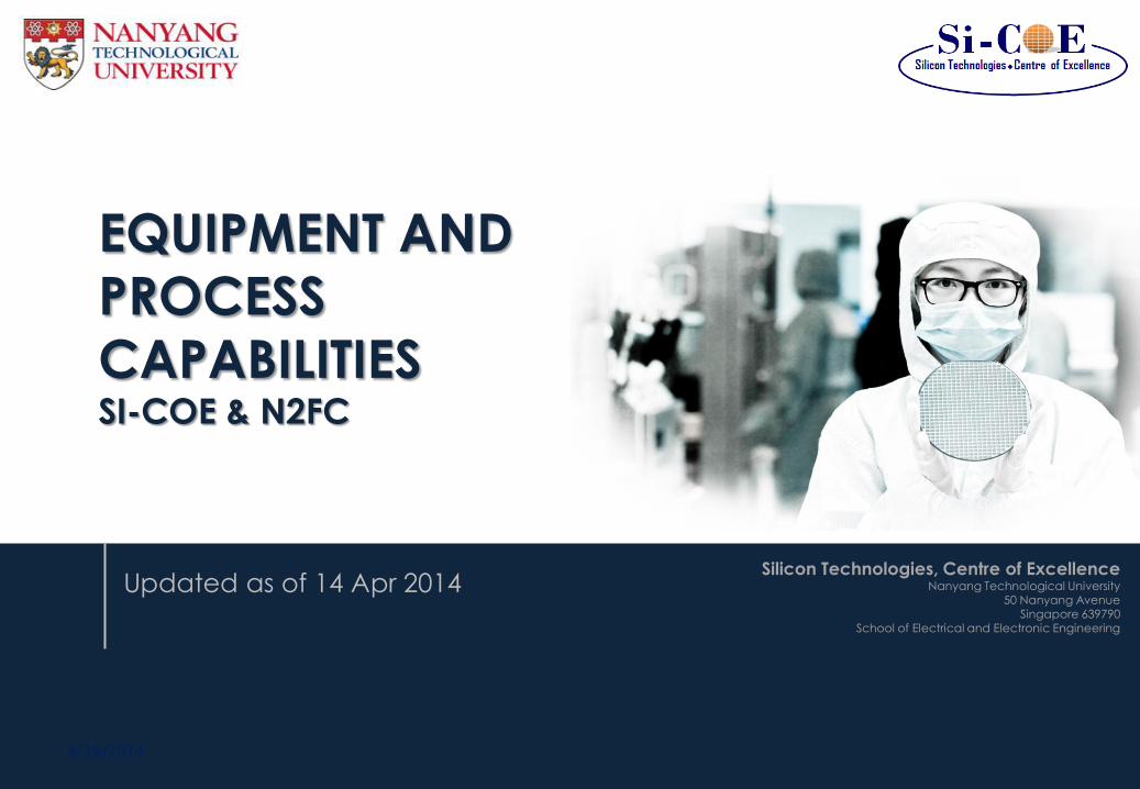
EQUIPMENT AND
PROCESS
CAPABILITIESSI-COE & N2FC
Updated as of 14 Apr 2014
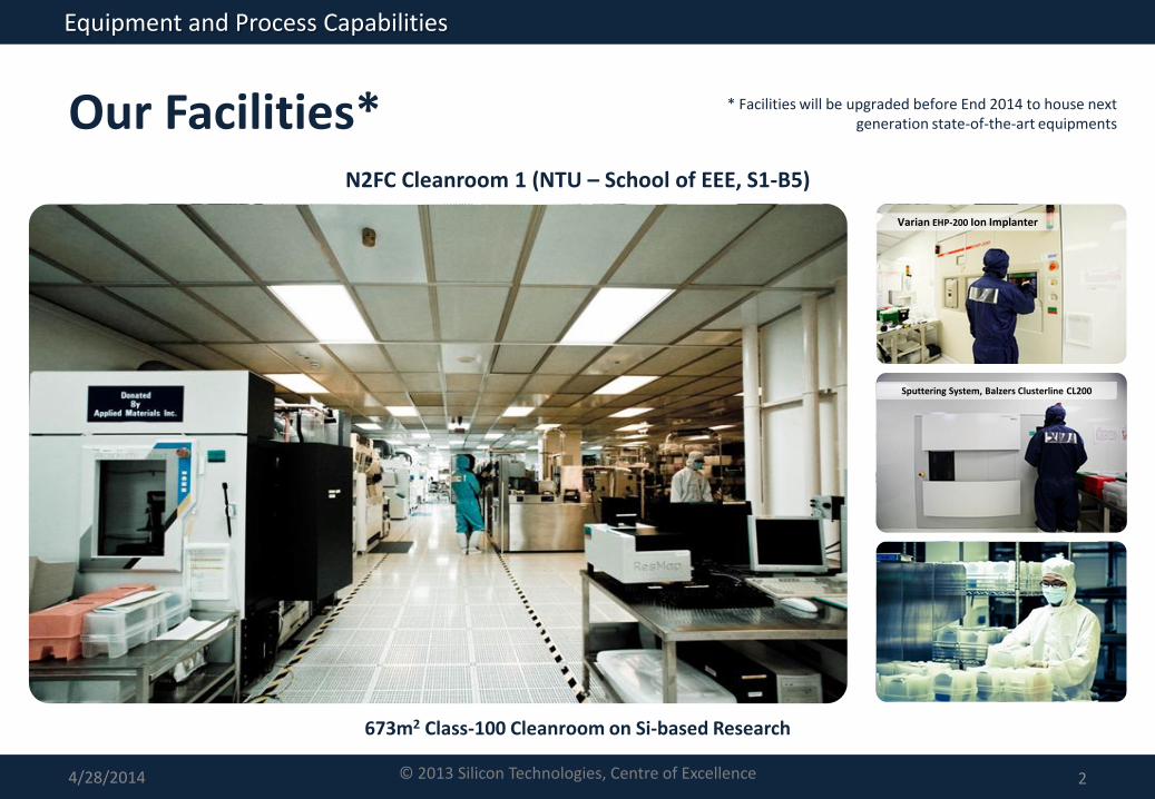
Our Facilities*
2
673m2 Class-100 Cleanroom on Si-based Research
N2FC Cleanroom 1 (NTU – School of EEE, S1-B5)
* Facilities will be upgraded before End 2014 to house next generation state-of-the-art equipments
Varian EHP-200 Ion Implanter
Sputtering System, Balzers Clusterline CL200
© 2013 Silicon Technologies, Centre of Excellence4/28/2014
Equipment and Process Capabilities
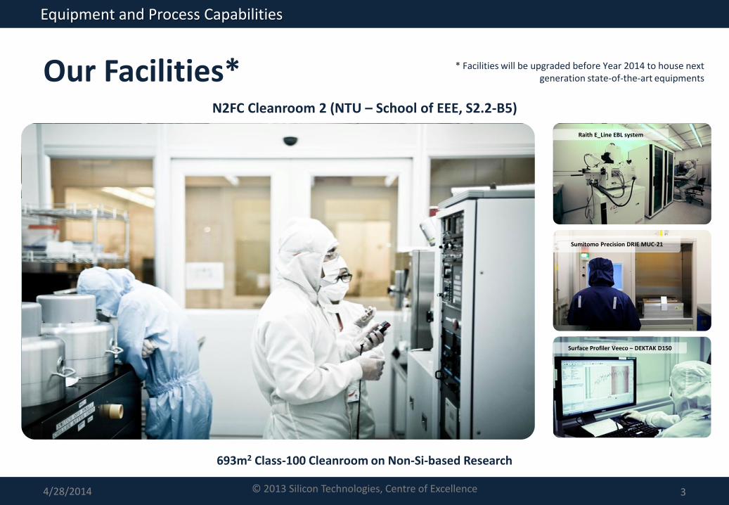
Our Facilities*
3
* Facilities will be upgraded before Year 2014 to house next generation state-of-the-art equipments
N2FC Cleanroom 2 (NTU – School of EEE, S2.2-B5)
693m2 Class-100 Cleanroom on Non-Si-based Research
Raith E_Line EBL system
Sumitomo Precision DRIE MUC-21
Surface Profiler Veeco – DEKTAK D150
© 2013 Silicon Technologies, Centre of Excellence4/28/2014
Equipment and Process Capabilities
4© 2013 Silicon Technologies, Centre of Excellence4/28/2014
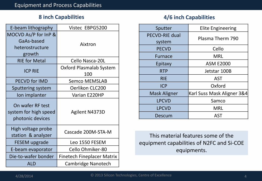
E-beam lithography Vistec EBPG5200
MOCVD As/P for InP & GaAs-based
heterostructure growth
Aixtron
RIE for Metal Cello Nasca-20L
ICP RIEOxford Plasmalab System
100
PECVD for IMD Semco MEMSLAB
Sputtering system Oerlikon CLC200
Ion implanter Varian E220HP
On wafer RF test system for high speed
photonic devices Agilent N4373D
High voltage probe station & analyzer
Cascade 200M-STA-M
FESEM upgrade Leo 1550 FESEM
E-beam evaporator Cello Ohmiker-80
Die-to-wafer bonder Finetech Fineplacer Matrix
ALD Cambridge Nanotech
Sputter Elite Engineering
PECVD-RIE dual system
Plasma Therm 790
PECVD Cello
Furnace MRL
Epitaxy ASM E2000
RTP Jetstar 100B
RIE AST
ICP Oxford
Mask Aligner Karl Suss Mask Aligner 3&4
LPCVD Samco
LPCVD MRL
Descum AST
8 inch Capabilities 4/6 inch Capabilities
Equipment and Process Capabilities
This material features some of the equipment capabilities of N2FC and Si-COE
equipments.
5© 2013 Silicon Technologies, Centre of Excellence4/28/2014
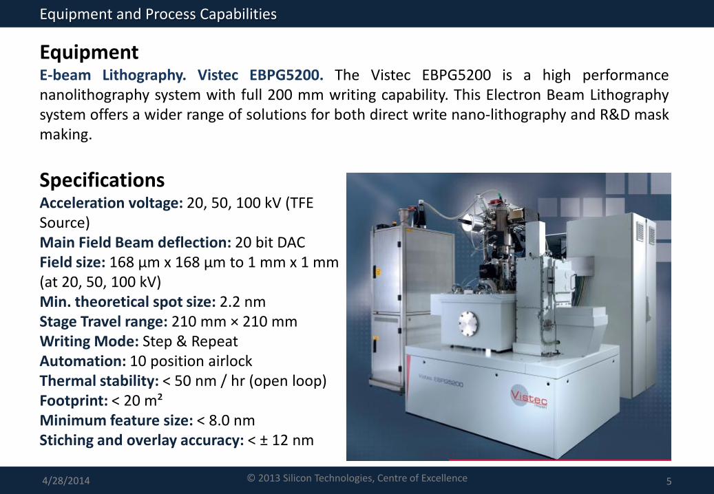
EquipmentE-beam Lithography. Vistec EBPG5200. The Vistec EBPG5200 is a high performancenanolithography system with full 200 mm writing capability. This Electron Beam Lithographysystem offers a wider range of solutions for both direct write nano-lithography and R&D maskmaking.
SpecificationsAcceleration voltage: 20, 50, 100 kV (TFE Source)Main Field Beam deflection: 20 bit DACField size: 168 μm x 168 μm to 1 mm x 1 mm (at 20, 50, 100 kV) Min. theoretical spot size: 2.2 nm Stage Travel range: 210 mm × 210 mm Writing Mode: Step & Repeat Automation: 10 position airlock Thermal stability: < 50 nm / hr (open loop) Footprint: < 20 m² Minimum feature size: < 8.0 nm Stiching and overlay accuracy: < ± 12 nm
Equipment and Process Capabilities
6© 2013 Silicon Technologies, Centre of Excellence4/28/2014
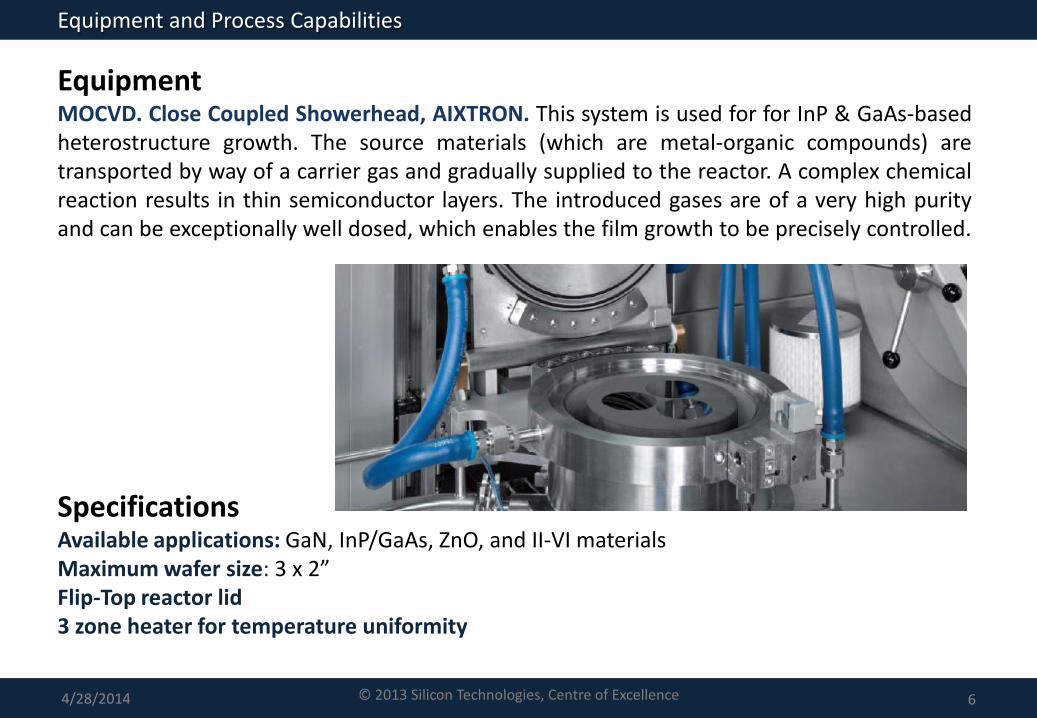
EquipmentMOCVD. Close Coupled Showerhead, AIXTRON. This system is used for for InP & GaAs-basedheterostructure growth. The source materials (which are metal-organic compounds) aretransported by way of a carrier gas and gradually supplied to the reactor. A complex chemicalreaction results in thin semiconductor layers. The introduced gases are of a very high purityand can be exceptionally well dosed, which enables the film growth to be precisely controlled.
SpecificationsAvailable applications: GaN, InP/GaAs, ZnO, and II-VI materialsMaximum wafer size: 3 x 2”Flip-Top reactor lid3 zone heater for temperature uniformity
Equipment and Process Capabilities
7© 2013 Silicon Technologies, Centre of Excellence4/28/2014
EquipmentRIE for Metal. Cello Nasca-20L, Cello Technology Co., Ltd. The Cello Nasca-20L Metal ReactiveIon Etching (MRIE) system provides capability of RIE etching of Metal materials. Clusteredmachine with one processing chamber and one loadlock chamber for transfer purpose. Wafersizes up to 8” diameters can be accommodated, as well as small random size pieces.
Process CapabilitiesAvailable gases: Cl2, BCl3, SF6, Ar, N2, O2
Helium mechanical clamp: AvailableMaximum wafer size: Up to 8”Typical targeted materials to be etched: Aluminum (Al), Titanium (Ti), Titanium Nitride (TiN),Tungsten (W) & etc.
Equipment and Process Capabilities
8© 2013 Silicon Technologies, Centre of Excellence4/28/2014
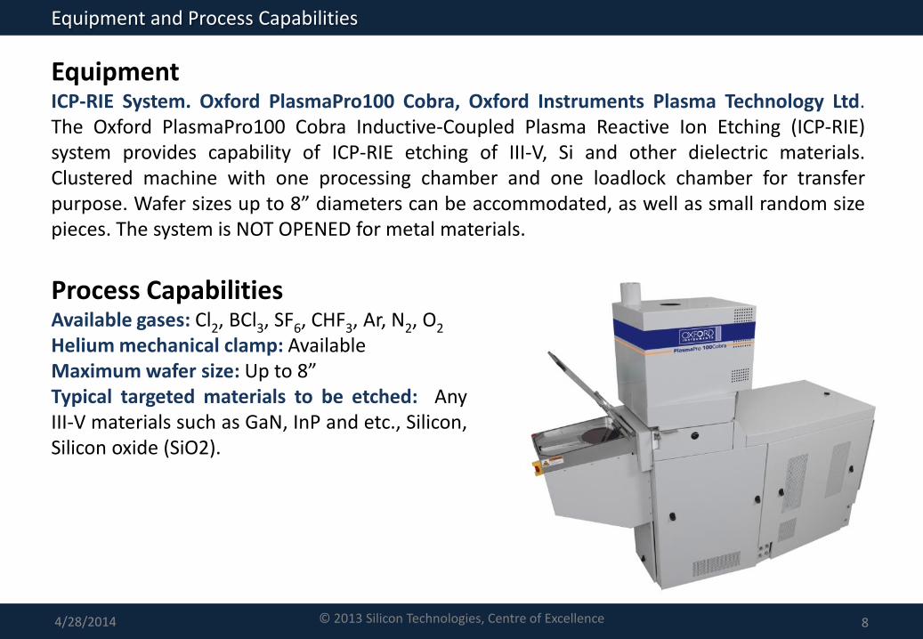
EquipmentICP-RIE System. Oxford PlasmaPro100 Cobra, Oxford Instruments Plasma Technology Ltd.The Oxford PlasmaPro100 Cobra Inductive-Coupled Plasma Reactive Ion Etching (ICP-RIE)system provides capability of ICP-RIE etching of III-V, Si and other dielectric materials.Clustered machine with one processing chamber and one loadlock chamber for transferpurpose. Wafer sizes up to 8” diameters can be accommodated, as well as small random sizepieces. The system is NOT OPENED for metal materials.
Process CapabilitiesAvailable gases: Cl2, BCl3, SF6, CHF3, Ar, N2, O2
Helium mechanical clamp: AvailableMaximum wafer size: Up to 8”Typical targeted materials to be etched: AnyIII-V materials such as GaN, InP and etc., Silicon,Silicon oxide (SiO2).
Equipment and Process Capabilities
9© 2013 Silicon Technologies, Centre of Excellence4/28/2014
EquipmentPECVD Deposition System. SEMCO MEMSLAB, SEMCO Engineering Inc. The SEMCOMEMSLAB PECVD deposition system provides capability of plasma enhanced chemical vapordeposition (PECVD) for silicon oxide, silicon nitride and amorphous silicon. Batch verticalfurnace type machine with front loaded vertical furnace chamber. Wafer sizes up to 8”diameters can be accommodated, as well as small random size pieces.
Process CapabilitiesAvailable gases: SiH4, N2O, NH3, SF6, O2 & N2
Allowable processing temperature: 380 CFurnace type: Batch VerticalMaximum number of processed wafers: 10 pcsMaximum wafer size: Up to 8”Typical targeted materials to be deposited: Silicon Oxide, Silicon Nitride and Silicon.
Equipment and Process Capabilities
10© 2013 Silicon Technologies, Centre of Excellence4/28/2014
EquipmentSputtering System. Oerlikon Clusterline CLC200, Oerlikon Systems Ltd. The OerlikonClusterline CLC200 Metal Sputtering system provides capability of metal sputtering for certainmetal materials. Clustered machine with two processing chambers, one soft-etch chamber,one transfer chamber, one cool chamber and one loadlock chamber. Wafer sizes up to 8”diameters can be accommodated, as well as small random size pieces by sticking onto 8”wafer substrate.
Process CapabilitiesAvailable gases: N2 and ArMaximum allowable temperature: 375 CMaximum wafer size: Up to 8”Types of metal targets: Aluminium (Al), Copper (Cu), Titanium (Ti) and Tantalum (Ta)Typical targeted materials to be sputtered: Aluminium (Al), Copper (Cu), Titanium (Ti),Tantalum (Ta), Titanium Nitride (TiN), Tantalum Nitride (TaN), Aluminium Nitride (AlN).
Equipment and Process Capabilities
11© 2013 Silicon Technologies, Centre of Excellence4/28/2014
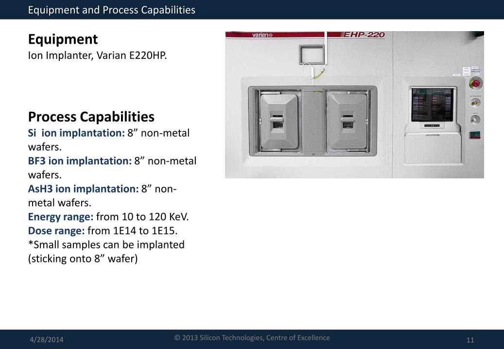
EquipmentIon Implanter, Varian E220HP.
Process CapabilitiesSi ion implantation: 8” non-metal wafers.BF3 ion implantation: 8” non-metal wafers.AsH3 ion implantation: 8” non-metal wafers.Energy range: from 10 to 120 KeV.Dose range: from 1E14 to 1E15.*Small samples can be implanted (sticking onto 8” wafer)
Equipment and Process Capabilities
12© 2013 Silicon Technologies, Centre of Excellence4/28/2014
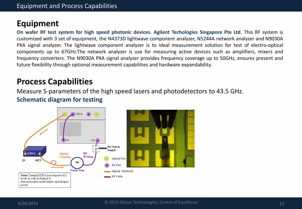
EquipmentOn wafer RF test system for high speed photonic devices. Agilent Techologies Singapore Pte Ltd. This RF system iscustomized with 3 set of equipment, the N4373D lightwave component analyzer, N5244A network analyzer and N9030APXA signal analyzer. The lightwave component analyzer is to ideal measurement solution for test of electro-opticalcomponents up to 67GHz.The network analyzer is use for measuring active devices such as amplifiers, mixers andfrequency converters. The N9030A PXA signal analyzer provides frequency coverage up to 50GHz, ensures present andfuture flexibility through optional measurement capabilities and hardware expandability.
Process CapabilitiesMeasure S-parameters of the high speed lasers and photodetectors to 43.5 GHz.Schematic diagram for testing
Equipment and Process Capabilities
13© 2013 Silicon Technologies, Centre of Excellence4/28/2014
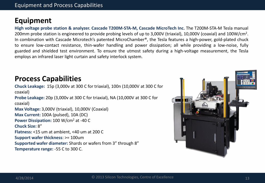
EquipmentHigh voltage probe station & analyzer. Cascade T200M-STA-M, Cascade MicroTech Inc. The T200M-STA-M Tesla manual200mm probe station is engineered to provide probing levels of up to 3,000V (triaxial), 10,000V (coaxial) and 100W/cm2.In combination with Cascade Microtech’s patented MicroChamber®, the Tesla features a high-power, gold-plated chuckto ensure low-contact resistance, thin-wafer handling and power dissipation; all while providing a low-noise, fullyguarded and shielded test environment. To ensure the utmost safety during a high-voltage measurement, the Teslaemploys an infrared laser light curtain and safety interlock system.
Process CapabilitiesChuck Leakage: 15p (3,000v at 300 C for triaxial), 100n (10,000V at 300 C for coaxial)Probe Leakage: 20p (3,000v at 300 C for triaxial), NA (10,000V at 300 C for coaxial)Max Voltage: 3,000V (triaxial), 10,000V (Coaxial)Max Current: 100A (pulsed), 10A (DC)Power Dissipation: 100 W/cm2 at -40 CChuck Size: 8”Flatness: <15 um at ambient, <40 um at 200 CSupport wafer thickness: >= 100umSupported wafer diameter: Shards or wafers from 3” through 8”Temperature range: -55 C to 300 C.
Equipment and Process Capabilities
14© 2013 Silicon Technologies, Centre of Excellence4/28/2014
EquipmentLEO 1550 FESEM. LEO 1550 Field Emission Scanning Electron Microscope (FESEM) is an ultra-high resolution field emission SEM utilizing the GEMINI field emission column. It is well suitedto a variety of applications owing to its versatile specimen chamber and large capacityCartesian stage.
Process CapabilitiesResolution: 1kV - 3nm, 20kV - 1nm Magnification: 20x to 200,000x Accelerating Voltage: 200V to 30kVSample Size: up to 6” wafer (available view field 3”).
Equipment and Process Capabilities
15© 2013 Silicon Technologies, Centre of Excellence4/28/2014
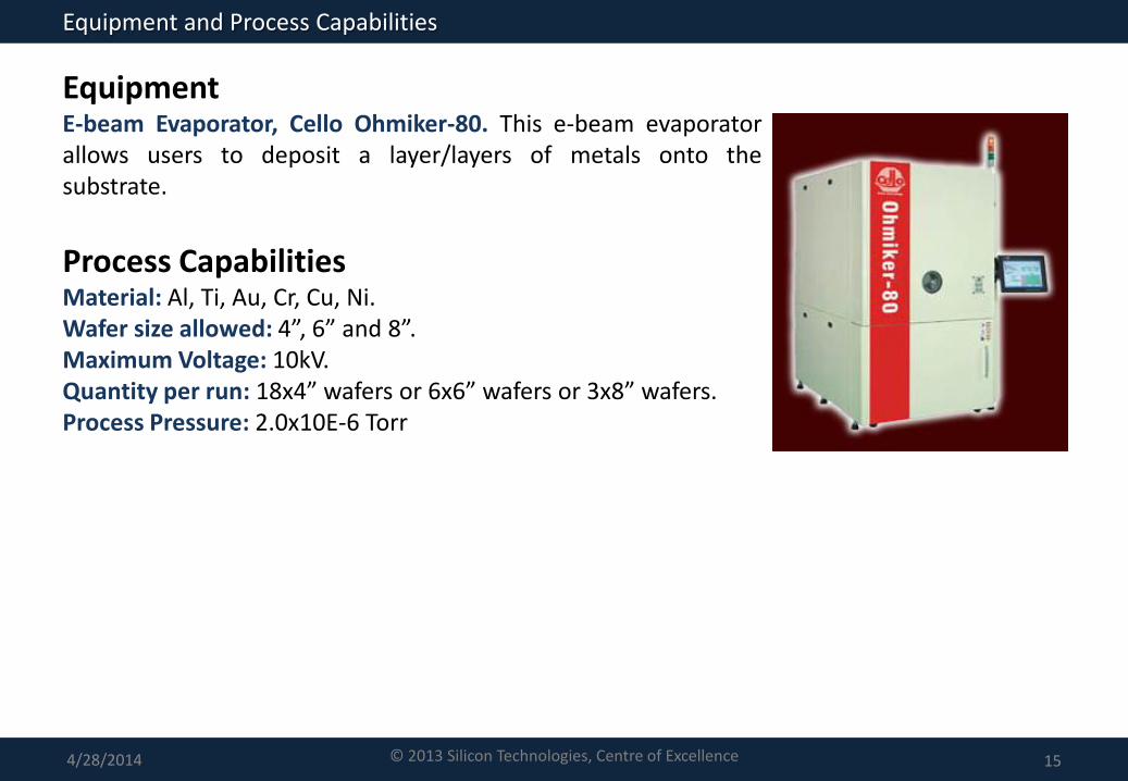
EquipmentE-beam Evaporator, Cello Ohmiker-80. This e-beam evaporatorallows users to deposit a layer/layers of metals onto thesubstrate.
Process CapabilitiesMaterial: Al, Ti, Au, Cr, Cu, Ni.Wafer size allowed: 4”, 6” and 8”.Maximum Voltage: 10kV.Quantity per run: 18x4” wafers or 6x6” wafers or 3x8” wafers. Process Pressure: 2.0x10E-6 Torr
Equipment and Process Capabilities
16© 2013 Silicon Technologies, Centre of Excellence4/28/2014
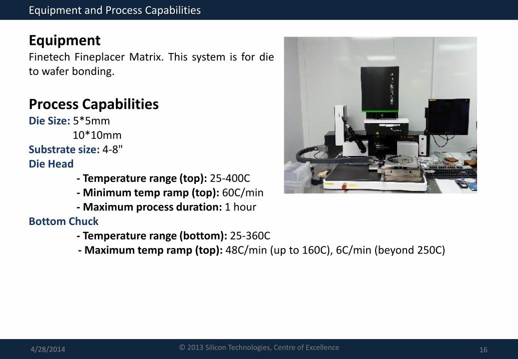
EquipmentFinetech Fineplacer Matrix. This system is for dieto wafer bonding.
Process CapabilitiesDie Size: 5*5mm
10*10mmSubstrate size: 4-8"Die Head
- Temperature range (top): 25-400C- Minimum temp ramp (top): 60C/min- Maximum process duration: 1 hour
Bottom Chuck- Temperature range (bottom): 25-360C- Maximum temp ramp (top): 48C/min (up to 160C), 6C/min (beyond 250C)
Equipment and Process Capabilities
17© 2013 Silicon Technologies, Centre of Excellence4/28/2014
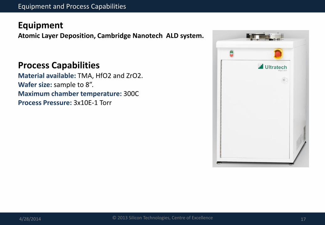
EquipmentAtomic Layer Deposition, Cambridge Nanotech ALD system.
Process CapabilitiesMaterial available: TMA, HfO2 and ZrO2.Wafer size: sample to 8”.Maximum chamber temperature: 300CProcess Pressure: 3x10E-1 Torr
Equipment and Process Capabilities
18© 2013 Silicon Technologies, Centre of Excellence4/28/2014
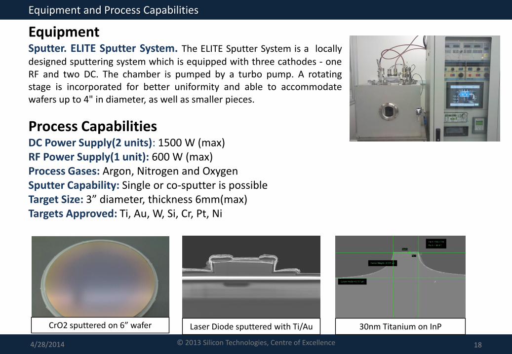
EquipmentSputter. ELITE Sputter System. The ELITE Sputter System is a locallydesigned sputtering system which is equipped with three cathodes - oneRF and two DC. The chamber is pumped by a turbo pump. A rotatingstage is incorporated for better uniformity and able to accommodatewafers up to 4" in diameter, as well as smaller pieces.
Process CapabilitiesDC Power Supply(2 units): 1500 W (max)RF Power Supply(1 unit): 600 W (max)Process Gases: Argon, Nitrogen and OxygenSputter Capability: Single or co-sputter is possibleTarget Size: 3” diameter, thickness 6mm(max)Targets Approved: Ti, Au, W, Si, Cr, Pt, Ni
CrO2 sputtered on 6” wafer Laser Diode sputtered with Ti/Au 30nm Titanium on InP
Equipment and Process Capabilities
19© 2013 Silicon Technologies, Centre of Excellence4/28/2014
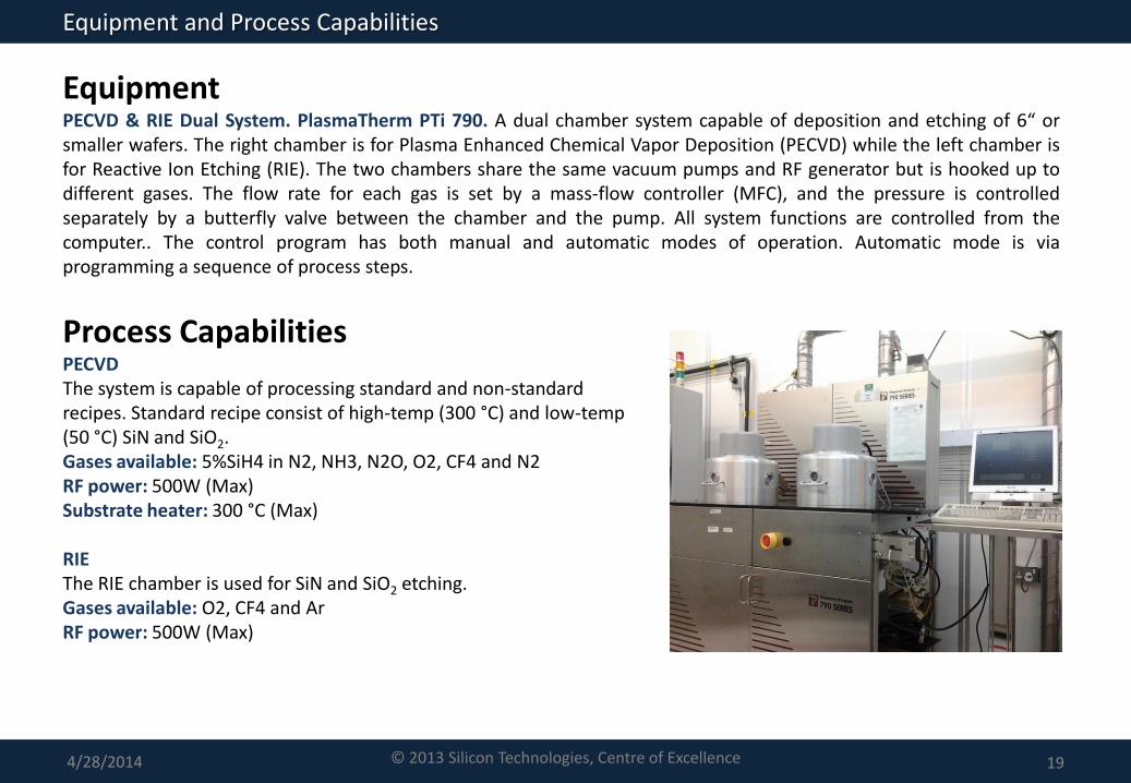
EquipmentPECVD & RIE Dual System. PlasmaTherm PTi 790. A dual chamber system capable of deposition and etching of 6“ orsmaller wafers. The right chamber is for Plasma Enhanced Chemical Vapor Deposition (PECVD) while the left chamber isfor Reactive Ion Etching (RIE). The two chambers share the same vacuum pumps and RF generator but is hooked up todifferent gases. The flow rate for each gas is set by a mass-flow controller (MFC), and the pressure is controlledseparately by a butterfly valve between the chamber and the pump. All system functions are controlled from thecomputer.. The control program has both manual and automatic modes of operation. Automatic mode is viaprogramming a sequence of process steps.
Process CapabilitiesPECVD The system is capable of processing standard and non-standard recipes. Standard recipe consist of high-temp (300 °C) and low-temp (50 °C) SiN and SiO2.Gases available: 5%SiH4 in N2, NH3, N2O, O2, CF4 and N2RF power: 500W (Max)Substrate heater: 300 °C (Max)
RIEThe RIE chamber is used for SiN and SiO2 etching.Gases available: O2, CF4 and ArRF power: 500W (Max)
Equipment and Process Capabilities
20© 2013 Silicon Technologies, Centre of Excellence4/28/2014
EquipmentPECVD Deposition System. Cello Aegis-20, Cello Technology Co., Ltd. The Cello Aegis-20PECVD deposition system provides capability of plasma enhanced chemical vapour deposition(PECVD) for silicon oxide, silicon nitride and amorphous silicon. Clustered machine with oneprocessing chamber and one loadlock chamber for transfer purpose. Wafer sizes up to 6”diameters can be accommodated, as well as small random size pieces.
Process CapabilitiesAvailable gases: SiH4, N2O, NH3, SF6 & N2
Allowable processing temperature: 200 & 300 CMaximum wafer size: Up to 6”Typical targeted materials to be deposited: Silicon Oxide, Silicon Nitride and Silicon.
Equipment and Process Capabilities
21© 2013 Silicon Technologies, Centre of Excellence4/28/2014
EquipmentMRL Furnaces. The MRL Furnaces are used for various thermal processes.
Process CapabilitiesMRL Drive in Furnace (Furnace A2): High temperature thermal process for 4”&6” non-metalwafers; maximum temperature 1150C; N2, H2 and O2 gases available.MRL Oxidation Furnace 1(Furnace A3): Dry oxide growth for 4”&6” non-metal wafers.MRL Oxidation Furnace 2(Furnace A4): Wet oxide growth for 4”&6” non-metal wafers.MRL POCL3 Furnace (Furnace B2): POCl3 doping at 950C for 4”&6” non-metal wafers.MRL Oxidation Furnace 3(Furnace B3): Annealing process for 4”&6” non-metal wafers,maximum temperature 1000C, N2, H2 and O2 gases available.MRL Alloy(Furnace B4): Annealing process for any kind of samples/wafers, maximumtemperature 1000C, N2, H2 and O2 gases available.
Equipment and Process Capabilities
22© 2013 Silicon Technologies, Centre of Excellence4/28/2014
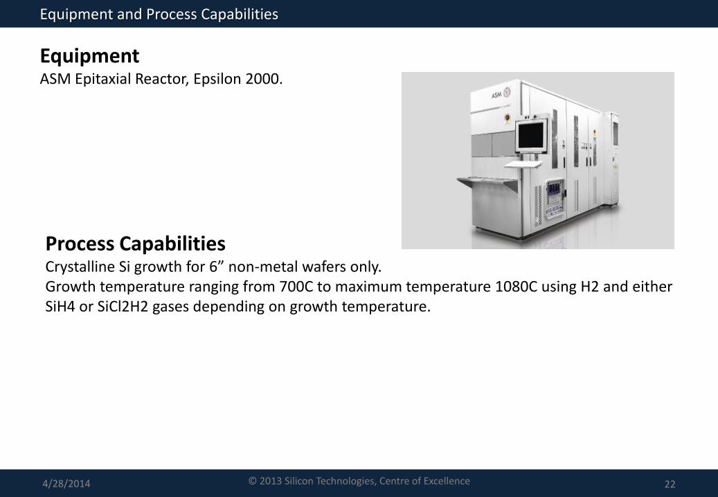
EquipmentASM Epitaxial Reactor, Epsilon 2000.
Process CapabilitiesCrystalline Si growth for 6” non-metal wafers only. Growth temperature ranging from 700C to maximum temperature 1080C using H2 and either SiH4 or SiCl2H2 gases depending on growth temperature.
Equipment and Process Capabilities
23© 2013 Silicon Technologies, Centre of Excellence4/28/2014
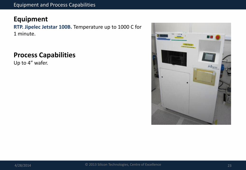
EquipmentRTP. Jipelec Jetstar 100B. Temperature up to 1000 C for1 minute.
Process CapabilitiesUp to 4” wafer.
Equipment and Process Capabilities
24© 2013 Silicon Technologies, Centre of Excellence4/28/2014
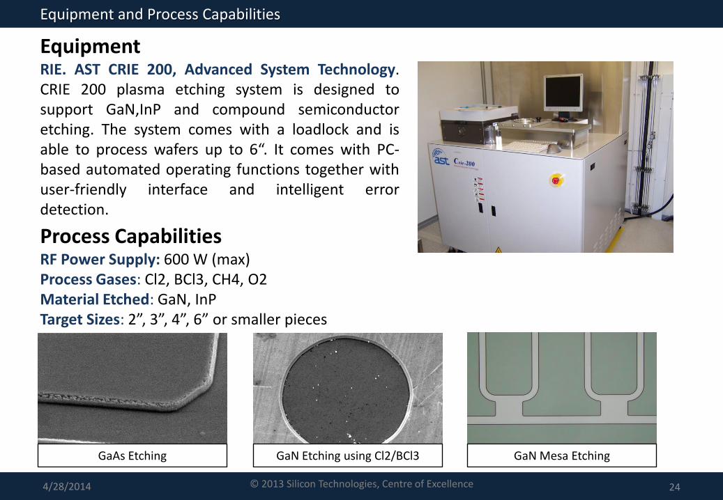
EquipmentRIE. AST CRIE 200, Advanced System Technology.CRIE 200 plasma etching system is designed tosupport GaN,InP and compound semiconductoretching. The system comes with a loadlock and isable to process wafers up to 6“. It comes with PC-based automated operating functions together withuser-friendly interface and intelligent errordetection.
Process CapabilitiesRF Power Supply: 600 W (max)Process Gases: Cl2, BCl3, CH4, O2Material Etched: GaN, InPTarget Sizes: 2”, 3”, 4”, 6” or smaller pieces
GaAs Etching GaN Etching using Cl2/BCl3 GaN Mesa Etching
Equipment and Process Capabilities
25© 2013 Silicon Technologies, Centre of Excellence4/28/2014
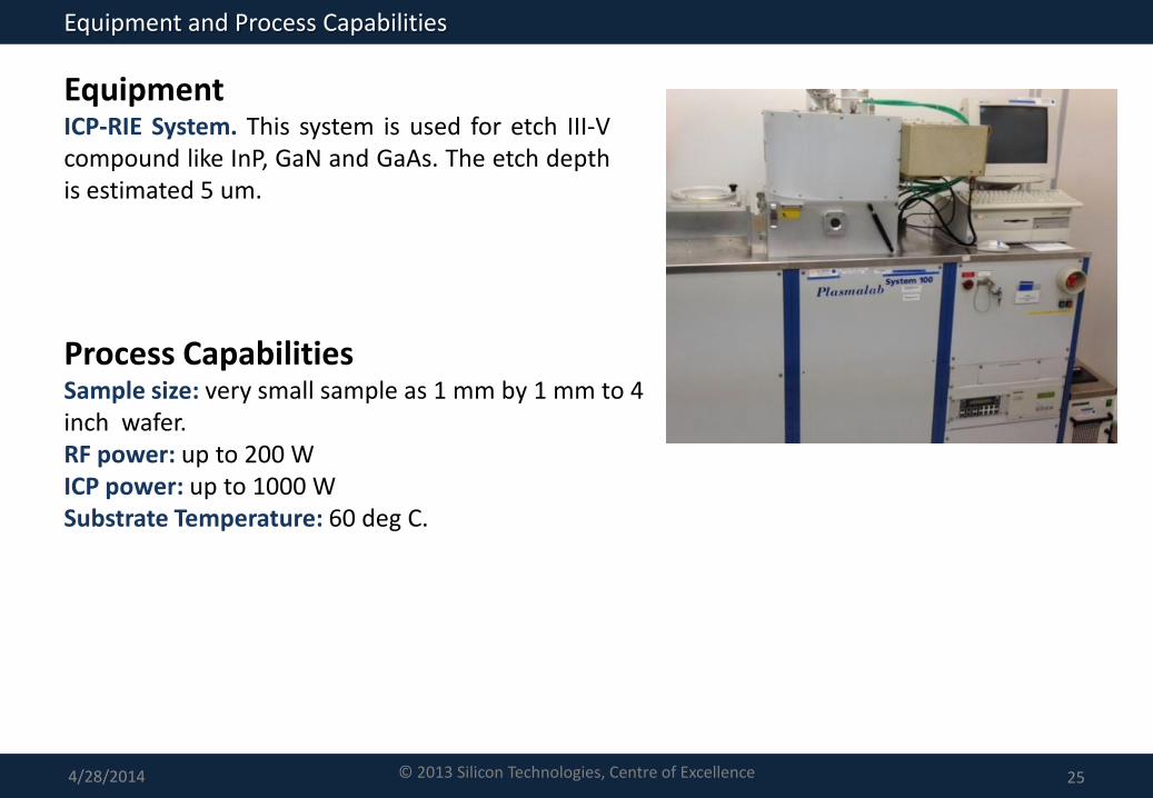
EquipmentICP-RIE System. This system is used for etch III-Vcompound like InP, GaN and GaAs. The etch depthis estimated 5 um.
Process CapabilitiesSample size: very small sample as 1 mm by 1 mm to 4 inch wafer.RF power: up to 200 WICP power: up to 1000 WSubstrate Temperature: 60 deg C.
Equipment and Process Capabilities
26© 2013 Silicon Technologies, Centre of Excellence4/28/2014
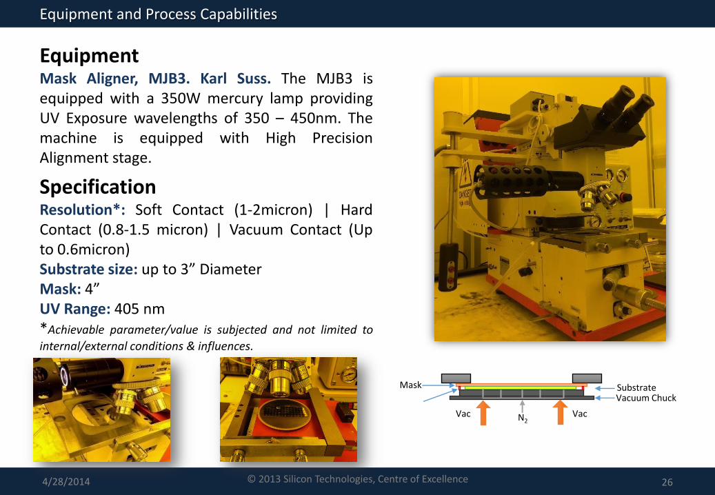
EquipmentMask Aligner, MJB3. Karl Suss. The MJB3 isequipped with a 350W mercury lamp providingUV Exposure wavelengths of 350 – 450nm. Themachine is equipped with High PrecisionAlignment stage.
SpecificationResolution*: Soft Contact (1-2micron) | HardContact (0.8-1.5 micron) | Vacuum Contact (Upto 0.6micron)Substrate size: up to 3” DiameterMask: 4”UV Range: 405 nm*Achievable parameter/value is subjected and not limited to
internal/external conditions & influences.
Mask SubstrateVacuum Chuck
N2Vac Vac
Equipment and Process Capabilities
27© 2013 Silicon Technologies, Centre of Excellence4/28/2014
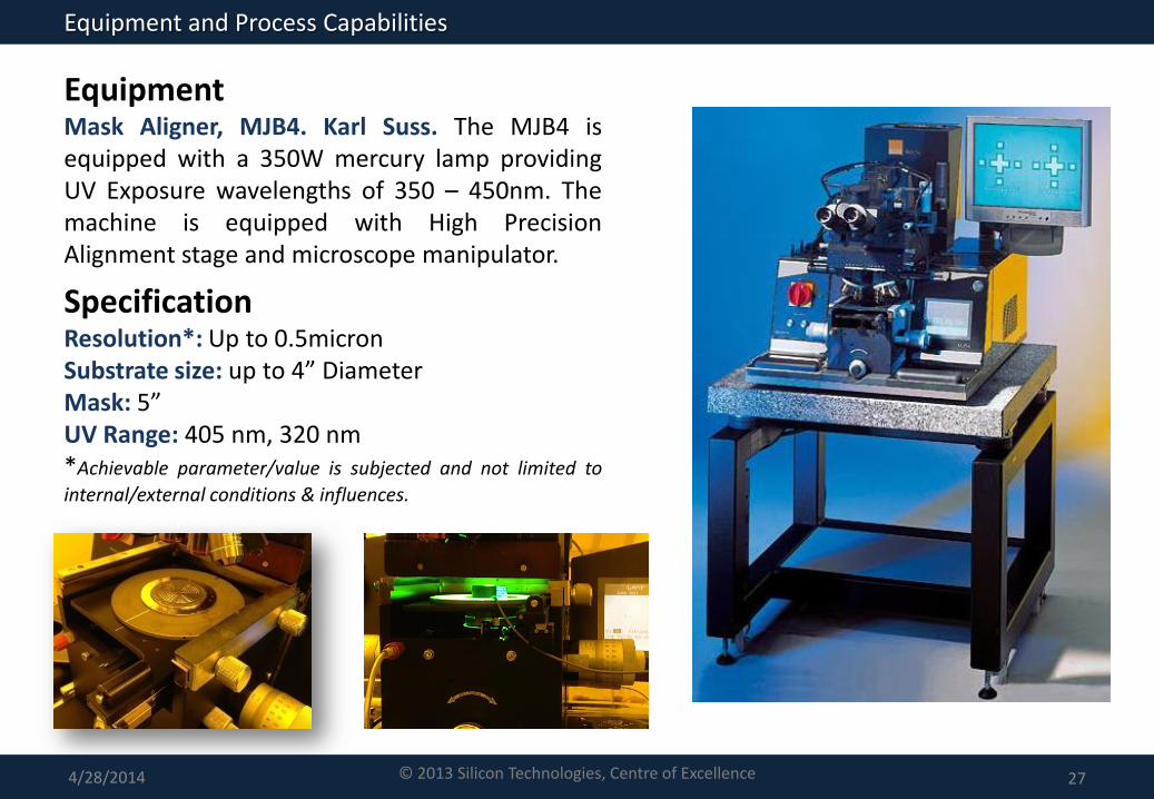
EquipmentMask Aligner, MJB4. Karl Suss. The MJB4 isequipped with a 350W mercury lamp providingUV Exposure wavelengths of 350 – 450nm. Themachine is equipped with High PrecisionAlignment stage and microscope manipulator.
SpecificationResolution*: Up to 0.5micronSubstrate size: up to 4” DiameterMask: 5”UV Range: 405 nm, 320 nm*Achievable parameter/value is subjected and not limited to
internal/external conditions & influences.
Equipment and Process Capabilities
28© 2013 Silicon Technologies, Centre of Excellence4/28/2014
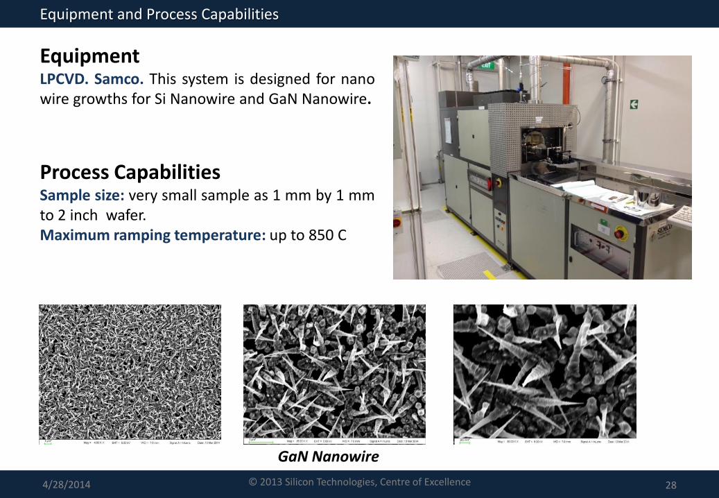
EquipmentLPCVD. Samco. This system is designed for nanowire growths for Si Nanowire and GaN Nanowire.
Process CapabilitiesSample size: very small sample as 1 mm by 1 mmto 2 inch wafer.Maximum ramping temperature: up to 850 C
GaN Nanowire
Equipment and Process Capabilities
29© 2013 Silicon Technologies, Centre of Excellence4/28/2014
EquipmentLPCVD, MRL. MRL low pressure chemical vapour deposition systems are used for SiN, Polysiand Teos deposition.
Process CapabilitiesMRL LPCVD SiN(MRL LPCVD C2): LS/HS SiN deposition for 4”&6” non-metal wafers.MRL LPCVD PolySi(MRL LPCVD C3): polysi deposition for 4”&6” non-metal wafers.MRL LPCVD TEOS(MRL LPCVD C4): teos deposition for 4”&6” non-metal wafers.
Equipment and Process Capabilities
30© 2013 Silicon Technologies, Centre of Excellence4/28/2014
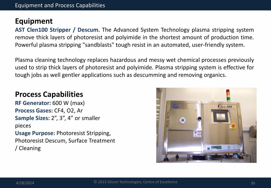
EquipmentAST Clen100 Stripper / Descum. The Advanced System Technology plasma stripping systemremove thick layers of photoresist and polyimide in the shortest amount of production time.Powerful plasma stripping "sandblasts" tough resist in an automated, user-friendly system.
Plasma cleaning technology replaces hazardous and messy wet chemical processes previouslyused to strip thick layers of photoresist and polyimide. Plasma stripping system is effective fortough jobs as well gentler applications such as descumming and removing organics.
Process CapabilitiesRF Generator: 600 W (max)Process Gases: CF4, O2, ArSample Sizes: 2”, 3”, 4” or smaller piecesUsage Purpose: Photoresist Stripping, Photoresist Descum, Surface Treatment / Cleaning
Equipment and Process Capabilities
The End
31
Introduction of Si-COE
© 2013 Silicon Technologies, Centre of Excellence4/28/2014